US6125157A - Delay-locked loop circuitry for clock delay adjustment - Google Patents
Delay-locked loop circuitry for clock delay adjustmentDownload PDFInfo
- Publication number
- US6125157A US6125157AUS08/795,657US79565797AUS6125157AUS 6125157 AUS6125157 AUS 6125157AUS 79565797 AUS79565797 AUS 79565797AUS 6125157 AUS6125157 AUS 6125157A
- Authority
- US
- United States
- Prior art keywords
- phase
- clock
- delay
- signal
- output
- Prior art date
- Legal status (The legal status is an assumption and is not a legal conclusion. Google has not performed a legal analysis and makes no representation as to the accuracy of the status listed.)
- Expired - Lifetime
Links
Images


Classifications
- H—ELECTRICITY
- H03—ELECTRONIC CIRCUITRY
- H03K—PULSE TECHNIQUE
- H03K5/00—Manipulating of pulses not covered by one of the other main groups of this subclass
- H03K5/13—Arrangements having a single output and transforming input signals into pulses delivered at desired time intervals
- H03K5/133—Arrangements having a single output and transforming input signals into pulses delivered at desired time intervals using a chain of active delay devices
- G—PHYSICS
- G06—COMPUTING OR CALCULATING; COUNTING
- G06F—ELECTRIC DIGITAL DATA PROCESSING
- G06F1/00—Details not covered by groups G06F3/00 - G06F13/00 and G06F21/00
- G06F1/04—Generating or distributing clock signals or signals derived directly therefrom
- G06F1/10—Distribution of clock signals, e.g. skew
- G—PHYSICS
- G11—INFORMATION STORAGE
- G11C—STATIC STORES
- G11C7/00—Arrangements for writing information into, or reading information out from, a digital store
- G11C7/22—Read-write [R-W] timing or clocking circuits; Read-write [R-W] control signal generators or management
- G—PHYSICS
- G11—INFORMATION STORAGE
- G11C—STATIC STORES
- G11C7/00—Arrangements for writing information into, or reading information out from, a digital store
- G11C7/22—Read-write [R-W] timing or clocking circuits; Read-write [R-W] control signal generators or management
- G11C7/222—Clock generating, synchronizing or distributing circuits within memory device
- H—ELECTRICITY
- H03—ELECTRONIC CIRCUITRY
- H03K—PULSE TECHNIQUE
- H03K5/00—Manipulating of pulses not covered by one of the other main groups of this subclass
- H03K5/22—Circuits having more than one input and one output for comparing pulses or pulse trains with each other according to input signal characteristics, e.g. slope, integral
- H03K5/24—Circuits having more than one input and one output for comparing pulses or pulse trains with each other according to input signal characteristics, e.g. slope, integral the characteristic being amplitude
- H03K5/2472—Circuits having more than one input and one output for comparing pulses or pulse trains with each other according to input signal characteristics, e.g. slope, integral the characteristic being amplitude using field effect transistors
- H03K5/2481—Circuits having more than one input and one output for comparing pulses or pulse trains with each other according to input signal characteristics, e.g. slope, integral the characteristic being amplitude using field effect transistors with at least one differential stage
- H—ELECTRICITY
- H03—ELECTRONIC CIRCUITRY
- H03L—AUTOMATIC CONTROL, STARTING, SYNCHRONISATION OR STABILISATION OF GENERATORS OF ELECTRONIC OSCILLATIONS OR PULSES
- H03L7/00—Automatic control of frequency or phase; Synchronisation
- H03L7/06—Automatic control of frequency or phase; Synchronisation using a reference signal applied to a frequency- or phase-locked loop
- H03L7/07—Automatic control of frequency or phase; Synchronisation using a reference signal applied to a frequency- or phase-locked loop using several loops, e.g. for redundant clock signal generation
- H—ELECTRICITY
- H03—ELECTRONIC CIRCUITRY
- H03L—AUTOMATIC CONTROL, STARTING, SYNCHRONISATION OR STABILISATION OF GENERATORS OF ELECTRONIC OSCILLATIONS OR PULSES
- H03L7/00—Automatic control of frequency or phase; Synchronisation
- H03L7/06—Automatic control of frequency or phase; Synchronisation using a reference signal applied to a frequency- or phase-locked loop
- H03L7/08—Details of the phase-locked loop
- H03L7/0805—Details of the phase-locked loop the loop being adapted to provide an additional control signal for use outside the loop
- H—ELECTRICITY
- H03—ELECTRONIC CIRCUITRY
- H03L—AUTOMATIC CONTROL, STARTING, SYNCHRONISATION OR STABILISATION OF GENERATORS OF ELECTRONIC OSCILLATIONS OR PULSES
- H03L7/00—Automatic control of frequency or phase; Synchronisation
- H03L7/06—Automatic control of frequency or phase; Synchronisation using a reference signal applied to a frequency- or phase-locked loop
- H03L7/08—Details of the phase-locked loop
- H03L7/081—Details of the phase-locked loop provided with an additional controlled phase shifter
- H03L7/0812—Details of the phase-locked loop provided with an additional controlled phase shifter and where no voltage or current controlled oscillator is used
- H03L7/0814—Details of the phase-locked loop provided with an additional controlled phase shifter and where no voltage or current controlled oscillator is used the phase shifting device being digitally controlled
- H—ELECTRICITY
- H03—ELECTRONIC CIRCUITRY
- H03L—AUTOMATIC CONTROL, STARTING, SYNCHRONISATION OR STABILISATION OF GENERATORS OF ELECTRONIC OSCILLATIONS OR PULSES
- H03L7/00—Automatic control of frequency or phase; Synchronisation
- H03L7/06—Automatic control of frequency or phase; Synchronisation using a reference signal applied to a frequency- or phase-locked loop
- H03L7/08—Details of the phase-locked loop
- H03L7/081—Details of the phase-locked loop provided with an additional controlled phase shifter
- H03L7/0812—Details of the phase-locked loop provided with an additional controlled phase shifter and where no voltage or current controlled oscillator is used
- H03L7/0816—Details of the phase-locked loop provided with an additional controlled phase shifter and where no voltage or current controlled oscillator is used the controlled phase shifter and the frequency- or phase-detection arrangement being connected to a common input
- H—ELECTRICITY
- H04—ELECTRIC COMMUNICATION TECHNIQUE
- H04L—TRANSMISSION OF DIGITAL INFORMATION, e.g. TELEGRAPHIC COMMUNICATION
- H04L7/00—Arrangements for synchronising receiver with transmitter
- H04L7/0016—Arrangements for synchronising receiver with transmitter correction of synchronization errors
- H04L7/0033—Correction by delay
- H04L7/0037—Delay of clock signal
- H—ELECTRICITY
- H03—ELECTRONIC CIRCUITRY
- H03K—PULSE TECHNIQUE
- H03K5/00—Manipulating of pulses not covered by one of the other main groups of this subclass
- H03K2005/00013—Delay, i.e. output pulse is delayed after input pulse and pulse length of output pulse is dependent on pulse length of input pulse
- H03K2005/00019—Variable delay
- H03K2005/00026—Variable delay controlled by an analog electrical signal, e.g. obtained after conversion by a D/A converter
- H03K2005/00032—DC control of switching transistors
- H—ELECTRICITY
- H03—ELECTRONIC CIRCUITRY
- H03K—PULSE TECHNIQUE
- H03K5/00—Manipulating of pulses not covered by one of the other main groups of this subclass
- H03K2005/00013—Delay, i.e. output pulse is delayed after input pulse and pulse length of output pulse is dependent on pulse length of input pulse
- H03K2005/00019—Variable delay
- H03K2005/00026—Variable delay controlled by an analog electrical signal, e.g. obtained after conversion by a D/A converter
- H03K2005/00052—Variable delay controlled by an analog electrical signal, e.g. obtained after conversion by a D/A converter by mixing the outputs of fixed delayed signals with each other or with the input signal
- H—ELECTRICITY
- H03—ELECTRONIC CIRCUITRY
- H03K—PULSE TECHNIQUE
- H03K5/00—Manipulating of pulses not covered by one of the other main groups of this subclass
- H03K2005/00013—Delay, i.e. output pulse is delayed after input pulse and pulse length of output pulse is dependent on pulse length of input pulse
- H03K2005/0015—Layout of the delay element
- H03K2005/00195—Layout of the delay element using FET's
- H03K2005/00208—Layout of the delay element using FET's using differential stages
- H—ELECTRICITY
- H04—ELECTRIC COMMUNICATION TECHNIQUE
- H04L—TRANSMISSION OF DIGITAL INFORMATION, e.g. TELEGRAPHIC COMMUNICATION
- H04L7/00—Arrangements for synchronising receiver with transmitter
- H04L7/0008—Synchronisation information channels, e.g. clock distribution lines
- H—ELECTRICITY
- H04—ELECTRIC COMMUNICATION TECHNIQUE
- H04L—TRANSMISSION OF DIGITAL INFORMATION, e.g. TELEGRAPHIC COMMUNICATION
- H04L7/00—Arrangements for synchronising receiver with transmitter
- H04L7/0016—Arrangements for synchronising receiver with transmitter correction of synchronization errors
- H04L7/002—Arrangements for synchronising receiver with transmitter correction of synchronization errors correction by interpolation
- H04L7/0025—Arrangements for synchronising receiver with transmitter correction of synchronization errors correction by interpolation interpolation of clock signal
Definitions
- the present inventionrelates to clock delay adjustment circuitry.
- the present inventionrelates to the generation of a set of phase vectors and the generation of output clocks that have precise phase relationships to an input clock.
- Previous artincludes the Rambus patent, U.S. Pat. No. 5,485,490, by Leung and Horowitz, which discloses two independent loops, the first of which creates a fixed number of phase vectors, the second of which creates an output clock that is in phase with the input clock. Also disclosed in this patent is the use of separate circuitry to create a leading phase clock to the output clock by selecting a pair of phase vectors and interpolating between them to produce an output that leads the output clock by the delay between phase vectors available from the first loop.
- Leediscloses a pair of delay-locked loops (DLL) for transmitting and receiving data in DRAMs.
- DLLdelay-locked loops
- IEEE Journal of Solid-State Circuits, Vol. 31, No. 4, April 1996, Tanoi et al.shows a two-loop architecture in which a frequency locked-loop (FLL) is designed to lock onto an external input frequency and to control the DLL for lock-in to the phase of the external input clock.
- FLLfrequency locked-loop
- Phase-locked loop circuitryemploying a VCO and single order loop filter to create phase vectors is a second order system.
- This second order systemhas stability problems associated with its operation.
- the VCO phase lock loopaccumulates phase error in response to sudden changes in phase on inputs to the loop, where the input includes not only the input clock but also the power supplies to the loop. This occurs because the loop changes the frequency of the VCO in response to a sudden phase change and this frequency shift is integrated to become phase error which persists for a time on the order of the reciprocal loop bandwidth (see Lee, above).
- the present inventionprovides delay-locked loop circuitry for generating a predetermined phase relationship between a pair of clocks.
- a first delay-locked loop (DLL)includes delay elements arranged in a chain, the chain receiving an input clock and generating, from the delay elements, a set of phase vectors, each shifted a unit delay from the adjacent vector.
- the first delay-locked loopadjusts the unit delays in the delay chain using a delay adjustment signal so that the phase vectors span a predetermined phase shift of the input clock.
- a second DLLis used, although the second DLL could be used with another circuit which produces two different delayed clock signals.
- the second DLLselects, from the first DLL, a pair of phase vectors which brackets the phase of an input clock.
- a phase interpolatorreceives the selected pair of vectors and generates an output clock and a delayed output clock, the amount of the delay being controlled by the delay adjustment signal of the first delay-locked loop circuitry.
- a phase detector in the second DLLcompares the delayed output clock with the input clock and adjusts the phase interpolator, based on the phase comparison, so that the phase of the delayed output clock is in phase with the input clock.
- the phase interpolatoris preferably adjusted with a control circuit including a digital memory for storing a count corresponding to the delay adjustment, which can be maintained in the absence of the input clock signal.
- the first DLLincludes a control circuit with a digital memory for providing the desired delay adjustment to the adjustable delay elements.
- a filteris used between the phase detector and the control circuit to reduce loop jitter.
- the present inventionis advantageously used for the transmit and receive clocks in a high-speed DRAM and a high-speed DRAM bus channel.
- FIG. 1shows a block diagram of a delay locked loop for generating phase vectors, K ⁇ r:0>;
- FIG. 2shows a more detailed block diagram than FIG. 1 of a delayed locked loop for generating phase vectors, K ⁇ r:0>, according to one embodiment
- FIG. 3shows a more detailed architecture than FIG. 2 of a delayed locked loop for generating phase vectors, K ⁇ r:0>, according to one embodiment
- FIG. 4shows another embodiment of a delay-locked loop for generating phase vectors using buffered delay elements and a buffer clock source.
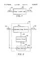
- FIG. 5shows a block diagram of the architecture of a DLL for generating an Output Clock in precise phase relationship with an Input Clock according to one embodiment
- FIG. 6shows a more detailed architecture than FIG. 5 of a DLL for generating an Output Clock in precise phase relationship with an Input Clock according to one embodiment
- FIG. 7shows another embodiment of a DLL for generating an Output Clock in precise phase relationship with an Input Clock using an adjustable delay section in the path of both the Output Clock and the feedback clock;
- FIG. 8shows another embodiment of an adjustable delay section having one adjustable delay for use in FIG. 7;
- FIG. 9shows another embodiment of an adjustable delay section having at least two adjustable delays for use in FIG. 7;
- FIG. 10shows an embodiment for producing a pair of delays from the same chain for use in FIG. 7;
- FIG. 11shows a set of four phase vectors each separated by a 90 degree interval and spanning 360 degrees shift of the 0 degree vector
- FIG. 12shows a set of eight phase vectors each separated by a 45 degree interval and spanning 360 degrees shift of the 0 degree vector
- FIG. 13shows a set of 12 phase vectors each separated by a 30 degree interval and spanning 360 degrees shift of the 0 degree vector
- FIG. 14shows a set of four phase vectors each separated by a 90 degree interval and spanning 360 degrees shift of the 0 degree vector, with the Input Clock and feedback clock between the 90 and 180 degree phase vectors and the Output Clock between the 0 and 90 degree vectors and 90 degrees earlier in time than the Input Clock;
- FIG. 15depicts a case in which the Input Clock is between the 135 and 180 degree phase vectors, with the initially selected phase vectors being the 0 and 45 degree vectors;
- FIG. 16Ashows an embodiment of a delay element for use in a delay-locked loop
- FIG. 16Bshows another embodiment of a delay element for use in a delay-locked loop
- FIG. 17shows an embodiment of a digital to analog converter for use in a delay-locked loop
- FIG. 18shows an embodiment of a phase interpolator for use in a delay-locked loop
- FIGS. 19A and 19Bshow an embodiment of a duty cycle correcting amplifier for use in a delay-locked loop.
- FIG. 19Ais the amplifier in which the duty cycle is corrected and
- FIG. 19Bis the duty cycle error detecting circuit which applies a correction signal to the amplifier in FIG. 19A;
- FIG. 20is a block diagram of a TrimAdj circuit for use in one variation of the embodiment of FIG. 7;
- FIG. 21is a circuit diagram of one embodiment of a phase detector as set forth in FIG. 6;
- FIG. 22is a block diagram of a DRAM system incorporating the present invention.
- Embodiments of the present inventionprovide a method and circuitry to generate a set of phase vectors in a way that is more immune to noise on loop inputs including the power supplies, leading to a more stable set of phase vectors.
- an output clockthat has a predetermined phase relationship with an input clock is provided. The effect of clock buffer delays between the input clock and output clock is minimized.
- the delay of an adjustable delay elementis adjusted with a counter and a digital-to-analog converter, the count in the counter digitally representing the current delay adjustment of the delay-locked loop. The digital count is converted to a signal suitable for adjusting an adjustable delay element used in a delay-locked loop.
- the current delay adjustment setting of the loopis digitally represented so that the setting may be stored while the loop is in a powered-down or low power state. There is quick re-acquisition of the locked state of a delay-locked loop after the delay-locked loop has been powered down.
- a delay-locked loopis employed for generating phase vectors.
- the DLL 100receives an external clock, ClkSrc 101, and generates phase vectors, K ⁇ r:0> 103.
- a convenient way to represent the set of phase vectors for a periodic signalis to draw the vectors in phase space as in FIG. 11. In this figure there are four vectors each spaced apart by 90 degrees and spanning a 360 degree phase shift of the 0 degree vector. Each vector in this figure represents a time delay of one-fourth of the cycle of the periodic signal.
- FIGS. 12 and 13show alternate sets of phase vectors.
- FIG. 12shows a set of vectors spaced at 45 degree intervals and spanning a 360 degree phase shift of the 0 degree vector.
- FIG. 13shows a set of vectors spaced at 30 degree intervals and spanning a 360 degree phase shift of the 0 degree vector.
- the DLL 100is a first order loop comprising at adjustable delay section 110, a control circuit 120 and a phase detector 130.
- the phase detector 130receives the external clock, ClkSrc 150 from which it derives a clock input ClkIn (not shown), a set of phase vector lines 140 and the last phase vector K ⁇ r> on line 160.
- the output of phase detector 130is coupled to the control circuit 120 which processes the output of the phase detector to generate a delay adjust signal 125 for adjusting the delay of the delay elements.
- the adjustable delay elementsare adjusted so that the phase of K ⁇ r> is the same as the clock input, ClkIn.
- FIG. 3shows an embodiment of the DLL in more detail.
- adjustable delay section 205comprises a set of four identical adjustable delay elements 210 connected in series with the output of each delay element 210 except the last element connected to the input of the next element 210. While four delay elements are shown in the particular embodiment, any number such as two, three, four, six, eight or twelve, can be used.
- This arrangementproduces a set of clocks, called phase vectors K ⁇ r:0> 270, each shifted in time from the next by a delay, called a unit delay, generated by the adjustable delay section 205.
- Each adjustable delay element 210receives the delay adjust signal DlyAdj 260 from control circuit 230, comprising counter control circuit 240 and digital-to-analog converter (DAC) 250.
- DlyAdj 260from control circuit 230, comprising counter control circuit 240 and digital-to-analog converter (DAC) 250.
- DACdigital-to-analog converter
- Counter control circuit 240receives an input, PhDiff 225, from phase detector 220 and generates count Cnt ⁇ c:0> 245 for input to the DAC.
- control circuit 230is implemented with digital circuits to permit the storage of the current delay adjustment setting of the loop, held by Cnt ⁇ c:0>245, during times when the ClkSrc 200 is not present, perhaps during a period when the system is shut down to save power. The saved setting permits the loop to quickly re-acquire a locked condition when the ClkSrc is reactivated.
- phase detector 220receives as inputs ClkIn 215 derived from the ClkSrc 200 via buffer 202 and the last phase vector K ⁇ r> 280.
- buffer 202performs duty cycle correction as well as amplification to assure that ClkIn 215 has a 50% duty cycle. Duty cycle correction is discussed in greater detail below.
- adjustable delay element 210may be implemented according to the embodiment shown in FIG. 16A, which shows a delay element 1010 and a bias circuit 1000.
- the delay elementis a differential delay element, having both true and complementary inputs and outputs.
- the circuitoperates to delay the differential inputs IN 1005 and IN -- B 1015 to produce delayed outputs Out 1130 and Out -- B 1140.
- the amount of delayis adjusted by adjustable current source 1020, which controls the amount of current switched by differential pair 1100 and 1110. The greater the amount of current switched the smaller delay produced by the differential pair.
- Transistors 1080 and 1090act as clamps to limit the swing of the differential pair allowing small delays to be realized by the circuit.
- the adjustable delay elementmay also be implemented according to the embodiment shown in FIG. 16B.
- section 1215functions as a fixed delay comprising a current source 1260 and a differential pair 1220 and 1230
- section 1225operates as a phase interpolator comprising differential pair 1330 and 1340 with current source 1320 and differential pair 1290 and 1300 with current source 1310 to produce a delay that is adjustable between a stage delay to a fixed delay plus the stage delay.
- the stage delayrepresents the fixed delay time through the interpolator stage 1225.
- the phase interpolator delay stage 1225is adjusted by varying the current sources Ix 1320 and Iy 1310.
- phase interpolator delay stage 1225is adjustable through a range of delay equal to the fixed delay of the 1215 section.
- FIG. 3depicts a DAC which may be implemented according to the DAC shown in FIG. 17, which depicts a circuit for converting a digital count Cnt ⁇ c:0> 1510 and its complement Cnt -- B ⁇ c:o> 1500 to a differential current pair, Ictl 1640 and Ictl -- B 1590 proportional to the count.
- FIG. 17shows three sections of circuitry, a set of binary weighted current sources 1520, a set of switches 1540 for producing the true current output Ictl 1640 and a set of switches 1530 for producing the complement output Ictl -- B 1590.
- Ictl 1640has a maximum current, Max -- I, which is the sum of all of the current sources 1650, 1660, 1670 through 1680 and the complementary current Ictl -- B is zero. If the count input Cnt ⁇ c:0> 1510 is all zeros then Ictl -- B 1590 has the maximum current, Max I, and Ictl is zero. Intermediate counts produce intermediate amounts of current, Im, and (Max -- I-Im) on Ictl and Ictl -- B respectively.
- This DACis suitable for controlling the differential input delay adjust signals of the adjustable delay element 210 shown in FIG. 16B for the delay-locked loop shown in FIG. 3.
- Phase detector 220compares the ClkIn signal, with the last phase vector K ⁇ r> 280 to determine the phase difference from a predetermined phase relationship between the two clocks.
- the predetermined phase differencecould be zero degrees.
- the predetermined phase differencecould be 180 degrees.
- the phase differenceis represented by signal PhDiff 225.
- Counter control blockthen converts the PhDiff signal into a digital count, Cnt ⁇ c:0> 245, and DAC 250 converts the count value into an analog quantity, DlyAdj 260, for adjusting the adjustable delay elements.
- the Cnt ⁇ c:0> signal and the DlyAdj signalmay be differential signals.
- the delay adjustmentoperates to change the delay of the adjustable delay elements so that the phase difference from the predetermined phase relationship between clock input, ClkIn and K ⁇ r> is made close to zero.
- the DLLis locked, and each adjustable delay element has substantially the same delay.
- each phase vectoris displaced in time from the adjacent vector by an amount equal to the setting of the adjustable delay element. This time displacement is termed a unit delay.
- the resultis that the phase vectors span a 360 degree phase shift of the ClkIn signal 215.
- an alternate embodimentcould use fewer delay elements to produce phase vectors that span the 360 degree phase shift of the ClkIn if each delay element, such as the ones depicted in FIGS. 16A and 16B, can produce both true and complementary outputs.
- each delay elementsuch as the ones depicted in FIGS. 16A and 16B
- two delay elements separated by 90 degreescould be used if the delay element had true outputs yielding delays of 90 and 180 degrees and complementary outputs yielding 270 and 360 degrees, respectively.
- fewer delay elementscould be used if the phase detector were designed to detect phase differences from a predetermined phase relationship of 180 degrees. Using such a phase detector would only require that two delay elements be used spanning a 180 degree phase shift of the ClkIn signal.
- the outputs of the delay elementscould be inverted in a separate circuit which receives the phase vectors, so that a set of phase vectors spanning 360 degrees is obtained.
- buffer 202may perform a duty cycle correction function to assure that the ClkIn signal 215 has a 50% duty cycle. This is especially important when the remaining span of 180 degrees is derived through inversion of the phase vectors spanning the first 180 degrees, because inversion will not generate the proper phase shift if the duty cycle is not substantially close to 50%.
- an additional adjustable delay elementhas been placed in the circuit to receive the last phase vector.
- This additional delayhas the effect of insuring that each phase vector has the identical loading as the other phase vectors, so that phase errors caused by loading differences are substantially eliminated.
- signal 265may be connected to a convenient voltage, because the output of the additional delay is not used. This eliminates some of the loading on the DlyAdj signal 260.
- phase vectors 275are buffered by buffers 212 in order to further control the loading on the vectors by isolating the loading of the phase vectors from other circuits which may receive the vectors.
- a buffered version of ClkIn 215 and a buffered version of the last phase vector K ⁇ r> 285are sent to the phase detector. This guarantees that buffered version of the phase vectors K ⁇ r:0> 275 are separated in phase by a unit delay and that the set of buffered phase vectors span a 360 degree or 180 degree shift of the buffered ClkIn signal depending upon the embodiment chosen.
- FIG. 4Also shown in FIG. 4 is a version of buffer 202 which has a duty cycle correcting circuit 290 attached.
- the duty cycle correcting circuit 290senses signal 214 for a deviation from a 50% duty cycle. It then feeds a correction signal to buffer 202 to correct signal 214.
- signal 214is a differential signal and the error signal 295 is a differential signal.
- FIGS. 19A and 19BAn embodiment of a duty cycle correcting amplifier is shown in FIGS. 19A and 19B.
- FIG. 19Ashows the correcting stage 2005 and the buffering stage 2055 and
- FIG. 19Bshows the duty cycle error detecting stage 2215.
- differential pair 1960 and 1970receive the input clock differential on In+ 1920 and In- 1930 and produce a differential output clock on Corr Clock -- B 2090 and Corr Clock 2100. If the duty cycle deviates from 50% then the circuit shown in FIG. 19B will produce a differential error voltage signal pair Error+ 2300 and Error- 2200 from the differential pair 2230 and 2250 and capacitor 2260 acting as an integrator.
- Transistors 2220, 2280, 2290 and 2270function as a load element especially suited for controlling the charge leakage across integrating capacitor 2260.
- the differential error voltage signal pairis fed back to the correcting stage 2005 such that the duty cycle error in the Corr Clock and Corr Clock -- B signals is reduced by altering currents 2110 and 2120 depending on the polarity of the error.
- the output of the buffering stage 2055is a clock having a duty cycle substantially close to 50%.
- Phase detector 220compares the ClkIn signal, with the last phase vector K ⁇ r> 280 to determine the phase difference from a predetermined phase relationship between the two clocks, and signal PhDiff 225 represents that difference.
- PhDiff signal 225contains random variations due to the instantaneous phase error which, when used directly by Counter Control 240, causes an amount of overall loop jitter, thus affecting the stability of the phase vectors.
- the amount of jitteris reduced by filtering the PhDiff signal before converting it to DlyAdj signal 260.
- control circuit 230includes filter 235 in addition to counter control 240 and digital to analog converter (DAC) 250.
- Filter circuit 235receives an input, PhDiff 225, from phase detector 220 and CntClk 241 from buffer 238 and generates output PhDiffF 237 for input to the Counter Control 240, which receives CntClk 241 and generates count Cnt ⁇ c:0> 245 for input to DAC 250.
- the PhDiff signalis a digital signal
- a digital filteris used, but either analog or digital filtering may be employed.
- CntClk 241operates the circuitry in both Filter 235 and Counter Control 240.
- Buffer 238is employed when ClkSrc is a small swing signal but Counter Control 240 and Filter 235 require a full swing signal.
- Types of digital filters that can be employed to reduce loop jitterinclude a majority-detector filter or an unanimity-detector filter.
- CntClk 241operates circuitry which samples and stores the state, either true or false, of PhDiff 225.
- a majority-detector filtersaves the last N samples, where N is an odd number, of PhDiff signal 225 and determines whether a majority of the last N cycles, say 3 out of 5 (N), are the same. If so, then the majority-detector filter activates PhDiffF 237 to alter the count in counter control 240. This type of filter alters the count in counter control 240 on every sample because there is always a majority of true or false samples.
- An unanimity-detector filteralso records the last N samples, where N can be even or odd, of the PhDiff signal but instead determines whether all N cycles are the same. If all samples are the same, the unanimity-detector filter activates the PhDiffF signal 237 to alter the count and at times during which not all the samples are the same, the PhDiffF signal will not be activated to alter the count. Both types of filters have the effect of reducing loop jitter, and either type may be used.
- the first delay-locked loop 320is one which generates phase vectors K ⁇ r:0> 330 from a clock source ClkSrc 300 as described above.
- the phase vectors and the DlyAdj signal 340are then used by a second delay-locked loop 350 to create a precise phase relationship between Input Clock 310 and Output Clock 360.
- FIG. 6shows an embodiment of the loop of FIG. 5 in more detail.
- First loop 400is the phase vector loop which receives ClkSrc 410 and generates phase vectors K ⁇ r:0> 430 and DlyAdj signal 440.
- the second loop 500is the loop for creating the phase relationship between the Input Clk 650 and Output Clk 640.
- Loop 500comprises a selection circuitry 510, phase interpolator 560, adjustable delay section 610 which represents an integer multiple of adjustable delay elements, clock buffers 620 and 630, control circuit 570 and phase detector 590.
- selection circuitry 510receives the phase vectors 430 and passes along a selected pair of vectors Kx 520 and Ky 530, which are received by phase interpolator 560.
- the phase interpolatorgenerates an interpolated output clock 615 which is buffered by clock buffer 620 to become the Output Clk 640.
- Adjustable delay section 610also receives output clock 615 and feeds the delayed clock to clock buffer 630 to generate FdBkClk 600.
- Control circuitgenerates PhAdj signal 550 for controlling the interpolator 560.
- Control circuit 570receives phase difference information, PhDiff 580, from phase detector 590, which detects the difference in phase between the Input Clk 650 and FdBkClk 600.
- control circuit 570may comprise counter control 240 and DAC 250 such as in FIG. 3, to enable the saving of the setting of the current phase adjustment of the loop or Filter 235, Counter Control 240 and DAC 250 as in FIG. 4 to additionally reduce loop jitter.
- Selection circuitry 510may be implemented as an analog or digital set of switches comprising a multiplexer, depending upon whether the phase vectors are low swing or full swing signals.
- Phase interpolator 560may be implemented as shown in FIG. 18. Alternately, selection circuitry 510 may be merged or combined with interpolator 560, shown in FIG. 6 as block 562. In some embodiments when selection circuitry is combined with the phase interpolator, the circuit shown in FIG. 18 is duplicated several times, each duplicate connected to a different set of switches for applying a particular phase vector to the interpolator.
- Differential pair 1800 and 1810receive one of the selected phase vectors Kx 1700 and Kx -- B 1740 which is the complement of the Kx signal.
- Kx and Kx -- Bmay be generated from a delay element having differential outputs as shown in FIG. 16A or 16B.
- Differential pair 1820 and 1830receive the Ky 1710 phase vector and the Ky -- B 1750 complementary phase vector.
- the phase interpolatorfunctions as a weighted integrator using capacitors C1 1760 and C2 1770 and coincidence detector 1860.
- Ictl 1720is set at a maximum value and Ictl -- B 1730 is zero then the output signal PIout 1870 is in phase with the Kx clock but delayed by a stage delay through the interpolator. If Ictl -- B 1730 is set a maximum value and Ictl 1720 is zero then the output signal is in phase with the Ky clock but delayed by a stage delay. By adjusting the values of adjustable currents 1720 and 1730 any delay between Kx and Ky may be achieved.
- phase detector 590determines what the difference in phase, if any, is between the Input Clk 650 and FdBkClk 600. This difference is then processed by control circuit 570 to select a pair of phase vectors via selection circuitry 510.
- the chosen pair of vectorsis that pair between which the phase of Input Clk 650 lies, after accounting for fixed delays inherent in circuits in the path of the FdBkClk signal such as the phase selector, phase interpolator, adjustable delay section and clock buffer.
- FIG. 14An example of a pair of vectors meeting this requirement is shown in FIG. 14, in which the Input Clk is shown between the 90 degree and 180 degree vectors and at a delay of alpha degrees from the 180 degree vector.
- FIG. 15depicts a circumstance in which the stepping of several phase vectors must occur if loop 500 starts in the 0 degree state before the correct pair is discovered.
- the phase interpolator 560is adjusted so that the phase interpolator output 615 is in phase with the 45 degree vector. While in this condition the 0 degree vector is replaced with the 90 degree vector by the control circuit and selection circuitry. Next, the phase interpolator is adjusted to produce an output in phase with the 90 degree vector and the 45 degree vector is replaced with the 135 degree vector.
- phase interpolatoris then adjusted to produce an output in phase with the 135 degree vector. Finally, the control circuit replaces the 90 degree vector with the 180 degree vector. Thus, while this stepping occurs the phase interpolator generates an output clock 615 which is in phase with one of the selected vectors, in particular, the one that will not be switched in selecting a new pair of vectors. The constraint that the interpolator generate the output clock in phase with the non-switched vector prevents the output clock from glitching during the stepping process.
- the phase interpolatoris allowed to be adjusted by PhAdj signal 550 to precisely align the delayed output FdBkClk 600 to the phase of the Input Clk 650, which is at some phase, alpha degrees, (FIG. 14) from one of the selected phase vectors.
- the loopis locked.
- FdBkClk 600is delayed by at least one unit delay from adjustable delay section 610, the unit delay being precisely a delay between any two adjacent phase vectors 430 from the first loop because it is adjusted by the same DlyAdj 440 signal of the first loop.
- phase interpolator 615assuming one delay element in block 610.
- FIG. 14shows this condition.
- Clock buffers 620 and 630are matched buffers having the same physical construction. FdBkClk is thus delayed by an amount equal to a unit delay and a clock buffer delay plus the other fixed delays from the phase selector and phase interpolator. However, because the Output Clk 640 is delayed by the same amount of fixed delays, the clock buffer delays and fixed delays cancel and the difference between the Output Clk 640 and the Input Clock 650 is only the unit delay.
- adjustable delay section 610could comprise an integer multiple of unit delays, in which case the delay between the Input Clk 650 and Output Clk 640 would then be the integer multiple of unit delays. For example, if the multiple of the unit delay is 3 and the value of the unit delay 10 degrees then the Output Clk would lead the Input Clk by 30 degrees. If the multiple of the unit delay is zero, then the Input Clk and Output Clk would be in phase.
- FIG. 7is an alternate embodiment showing adjustable delay section 612 in the path of the Output Clk 640.
- This sectionhas the same implementation as the section in the path of the FdBkClk 600 and provides a way for the Output Clk 640 to not only lead the Input Clk in phase but to lag it in phase.
- This latter conditionoccurs when the adjustable delay section 612 comprises a larger multiple of unit delays than adjustable delay section 610.
- Adjustable delay sections 612 and 610may be implemented in a fashion similar to section 206 in FIG. 4 in order to insure that phase errors due to loading differences are minimized.
- the delay circuits shown in FIGS. 16A and 16Bare suitable for implementing an adjustable delay element employed in the adjustable delay section 610 or 612.
- FIG. 16A and 16Bare suitable for implementing an adjustable delay element employed in the adjustable delay section 610 or 612.
- FIG. 7also shows that buffers 620 and 630 may be implemented as duty cycle correcting amplifiers with the aid of duty cycle correction circuit 670. Buffers 620 and 630 may be implemented according to the circuitry shown in FIG. 19A and duty cycle correction circuit 670 may be implemented as shown in FIG. 19B.
- FIG. 7shows three more inputs, Fast 575,Test 585 and ExtIn 595, to the control circuit 570.
- Fast signal 575is used to alter the control circuit so that the loop can lock more quickly by taking larger phase adjustments toward the lock condition.
- the control circuit 570is implemented as a counter
- the Fast signal 575can cause the counter to count by a multiple of the smallest step between counts.
- the Test signal 585is used to allow the control circuit to be under the control of external signal ExtIn 595 rather than PhDiff 580 derived from the loop. This allows loop properties to be tested more easily.
- FIG. 8shows one embodiment of adjustable delay section 612.
- Block 612comprises a buffer 702, similar to 202 in FIG. 4, an adjustable delay element 710 similar to adjustable delay element 210 in FIG. 4, and an output buffer 712 similar to the 212 buffer in FIG. 4.
- FIG. 9shows an embodiment of adjustable delay section 610. This figure is similar to FIG. 8 but has more adjustable delay elements, but is still buffered at the front of the chain and has an additional delay element at the end of the chain.
- the adjustable delay sections in both FIG. 8 and FIG. 9are controlled from an external delay adjust signal such as 441 as shown in FIG. 7, such that the setting produces a delay equal to the delay between phase vectors.
- adjustable delay sections 610 and 612are implemented in this fashion, loading differences are kept to a minimum and only the desired phase difference between signal 617 and 618 is generated. As may be easily seen it is not necessary that adjustable delay sections 610 and 612 be implemented as two separate and distinct sections. It is convenient in some embodiments to derive 617 and 618 from the same section 625 as shown in FIG. 7 and 10.
- the delay adjust signal 441 in FIG. 7is buffered by buffer 442, in some embodiments, to isolate the loading effects of sections 610 and 612 from section 420.
- FIG. 20discloses circuitry for biasing the predetermined phase relationship between the input clock and the output clock with a fixed offset.
- the fixed offsetis necessary when system requirements dictate that the predetermined phase relationship be altered by an amount that is smaller than is available from a unit a delay, for example a one degree phase shift.
- This fine tuning or trimmingis accomplished by the TrimAdj signal 2300 which is combined with the DlyAdj signal 441 in FIG. 7.
- the TrimAdj signal 2300adds a small amount of adjustment current to the adjustable delay sections 610 and 612. This causes the delay elements in those sections to have a delay that is slightly smaller or larger than the unit delay provided by the delay adjustment signal from the loop which generates the phase vectors.
- the TrimAdj signal 2300is derived from DAC 2310 and trim word storage 2320.
- Trim word storagein some embodiments is a set of fuses or other permanent storage for holding a digital code TW ⁇ t:0> 2330 for setting the trim delay.
- DAC 2310converts the trim word 2330 to an analog signal such as a current for controlling the delay elements in sections 610 and 612.
- FIG. 21is a circuit diagram of a phase detector circuit which could be used for the phase detector of FIGS. 2, 3, 4, 6 and 7.
- a clock input 2530is shown, and data input 2540 would correspond to the feedback clock or phase vector.
- Output 3000is the phase difference signal provided to the control circuit.
- the phase detectoris implemented as three blocks 2500, 2510, and 2520 connected in flip-flop fashion using NAND gates 2550, 2560, 2570, 2580, 2590, and 2595.
- FIG. 22shows a system application for the delay-locked loops of the present invention.
- master device 3100communicates with slave device 3110 or slave device 3120.
- Slave devices 3110 or 3120may communicate with master device 3100 but not with each other.
- the systemoperates from a pair of clocks generated from oscillator 3170 which generates CTM (Clock To Master) 3140 and CFM (Clock From Master) 3130.
- CTMtravels in the direction from the slave device to the master device and is used for transmitting data to the master on data bus 3150.
- CTMis looped back to generate CFM which travels in the direction from master to slave device and is used for transmitting data from the master to the slave device.
- Each device, master or slavehas a data receiver Rcvr 3180 and a data transmitter Txmtr 3190 for receiving and sending data respectively.
- the Rcvr 3180uses a signal rclk 3220 to receive the data from the data Bus and Txmtr 3190 uses tclk 3230 to transmit the data onto the data bus.
- Signals rclk and tclkare generated from a pair of delay-locked loops 3200 and 3205 in the slave and from a single delay-locked loop 3235 in the master, because the master makes no distinction between CTM and CFM.
- DLLR 3210is the delay-locked loop for generating the phase vectors and is called the reference loop. Each device uses a single DLLR loop.
- DLLF 3200is the delay-locked loop for generating a predetermined phase relationship between the input clock and the output clock.
- the DLLF 3200 loopis used to generate a 90 degree phase relationship between CTM and tclk, because data is always transmitted in quadrature to the receive clock.
- the DLLF 3205is used to generate a zero degree phase relationship between CFM and rclk.
- the masterreceives the clock CTM and generates the rclk signal for operating its receiver.
- Signal rclk in the masteris in a 0 degree phase relationship with CTM so that the data is sampled when it is not changing.
- the mastersends data to a slave, it clocks its transmitter changing the data on the data bus with tclk which is in a 90 degree phase relationship with the CFM.
- a slave 3110 receiving the data in its receiver 3180operates its receiver using rclk which has a 0 degree phase relationship with the CFM.
- the receiverwill sample the data when it is not changing. In this manner, data may be transmitted using both edges of the CTM or CFM clocks and safely sampled in the receiver.
- the master of FIG. 22is an intelligent device, such as a microprocessor, an application specific integrated circuit (ASIC), a memory controller, or a graphics engine.
- the slave devicesmay be DRAMs, SRAMs, ROMs, EPROMs, flash memories, or other memory devices.
Landscapes
- Engineering & Computer Science (AREA)
- Physics & Mathematics (AREA)
- Nonlinear Science (AREA)
- Theoretical Computer Science (AREA)
- Computer Networks & Wireless Communication (AREA)
- Signal Processing (AREA)
- General Engineering & Computer Science (AREA)
- General Physics & Mathematics (AREA)
- Stabilization Of Oscillater, Synchronisation, Frequency Synthesizers (AREA)
- Pulse Circuits (AREA)
- Dram (AREA)
Abstract
Description
The present invention relates to clock delay adjustment circuitry. In particular, the present invention relates to the generation of a set of phase vectors and the generation of output clocks that have precise phase relationships to an input clock.
Previous art includes the Rambus patent, U.S. Pat. No. 5,485,490, by Leung and Horowitz, which discloses two independent loops, the first of which creates a fixed number of phase vectors, the second of which creates an output clock that is in phase with the input clock. Also disclosed in this patent is the use of separate circuitry to create a leading phase clock to the output clock by selecting a pair of phase vectors and interpolating between them to produce an output that leads the output clock by the delay between phase vectors available from the first loop.
IEEE Journal of Solid-State Circuits, Vol. 29, No. 12, December 1994, Lee, et. al. ("Lee") discloses a pair of delay-locked loops (DLL) for transmitting and receiving data in DRAMs. IEEE Journal of Solid-State Circuits, Vol. 31, No. 4, April 1996, Tanoi et al. shows a two-loop architecture in which a frequency locked-loop (FLL) is designed to lock onto an external input frequency and to control the DLL for lock-in to the phase of the external input clock.
It is desirable to improve on the generation of a leading output clock to the in-phase output clock. There are several drawbacks to the invention disclosed in U.S. Pat. No. 5,485,490. Phase-locked loop circuitry employing a VCO and single order loop filter to create phase vectors is a second order system. This second order system has stability problems associated with its operation. Furthermore, the VCO phase lock loop accumulates phase error in response to sudden changes in phase on inputs to the loop, where the input includes not only the input clock but also the power supplies to the loop. This occurs because the loop changes the frequency of the VCO in response to a sudden phase change and this frequency shift is integrated to become phase error which persists for a time on the order of the reciprocal loop bandwidth (see Lee, above). This causes the loop to be noise sensitive when the noise is in the form of sudden phase shifts. Another drawback regarding the prior art patent is that the subloop used for generating the in-phase clock relies on the accuracy and similarity of a second phase interpolator (out-of-phase phase interpolator) to produce the leading clock. Any lack of matching between the out-of-phase phase interpolator and the in-phase phase interpolator will create a phase error in the desired phase relationship between the leading clock and the in-phase clock. Another drawback concerns the acquisition time of the VCO which can be quite long after restoration of a lost input clock, depending on how long the input clock has been absent.
The present invention provides delay-locked loop circuitry for generating a predetermined phase relationship between a pair of clocks. A first delay-locked loop (DLL) includes delay elements arranged in a chain, the chain receiving an input clock and generating, from the delay elements, a set of phase vectors, each shifted a unit delay from the adjacent vector. The first delay-locked loop adjusts the unit delays in the delay chain using a delay adjustment signal so that the phase vectors span a predetermined phase shift of the input clock.
In a preferred embodiment, a second DLL is used, although the second DLL could be used with another circuit which produces two different delayed clock signals. The second DLL selects, from the first DLL, a pair of phase vectors which brackets the phase of an input clock. A phase interpolator receives the selected pair of vectors and generates an output clock and a delayed output clock, the amount of the delay being controlled by the delay adjustment signal of the first delay-locked loop circuitry.
Preferably, a phase detector in the second DLL compares the delayed output clock with the input clock and adjusts the phase interpolator, based on the phase comparison, so that the phase of the delayed output clock is in phase with the input clock. The phase interpolator is preferably adjusted with a control circuit including a digital memory for storing a count corresponding to the delay adjustment, which can be maintained in the absence of the input clock signal.
Preferably, the first DLL includes a control circuit with a digital memory for providing the desired delay adjustment to the adjustable delay elements. A filter is used between the phase detector and the control circuit to reduce loop jitter.
The present invention is advantageously used for the transmit and receive clocks in a high-speed DRAM and a high-speed DRAM bus channel.
Other objects, features, and advantages of the present invention will be apparent from the accompanying drawings and from the detailed description which follows below.
The features and advantages of the present invention are illustrated by way of example and are by no means intended to limit the scope of the present invention to the particular embodiments shown, and in which:
FIG. 1 shows a block diagram of a delay locked loop for generating phase vectors, K<r:0>;
FIG. 2 shows a more detailed block diagram than FIG. 1 of a delayed locked loop for generating phase vectors, K<r:0>, according to one embodiment;
FIG. 3 shows a more detailed architecture than FIG. 2 of a delayed locked loop for generating phase vectors, K<r:0>, according to one embodiment;
FIG. 4 shows another embodiment of a delay-locked loop for generating phase vectors using buffered delay elements and a buffer clock source.
FIG. 5 shows a block diagram of the architecture of a DLL for generating an Output Clock in precise phase relationship with an Input Clock according to one embodiment;
FIG. 6 shows a more detailed architecture than FIG. 5 of a DLL for generating an Output Clock in precise phase relationship with an Input Clock according to one embodiment;
FIG. 7 shows another embodiment of a DLL for generating an Output Clock in precise phase relationship with an Input Clock using an adjustable delay section in the path of both the Output Clock and the feedback clock;
FIG. 8 shows another embodiment of an adjustable delay section having one adjustable delay for use in FIG. 7;
FIG. 9 shows another embodiment of an adjustable delay section having at least two adjustable delays for use in FIG. 7;
FIG. 10 shows an embodiment for producing a pair of delays from the same chain for use in FIG. 7;
FIG. 11 shows a set of four phase vectors each separated by a 90 degree interval and spanning 360 degrees shift of the 0 degree vector;
FIG. 12 shows a set of eight phase vectors each separated by a 45 degree interval and spanning 360 degrees shift of the 0 degree vector;
FIG. 13 shows a set of 12 phase vectors each separated by a 30 degree interval and spanning 360 degrees shift of the 0 degree vector;
FIG. 14 shows a set of four phase vectors each separated by a 90 degree interval and spanning 360 degrees shift of the 0 degree vector, with the Input Clock and feedback clock between the 90 and 180 degree phase vectors and the Output Clock between the 0 and 90 degree vectors and 90 degrees earlier in time than the Input Clock;
FIG. 15 depicts a case in which the Input Clock is between the 135 and 180 degree phase vectors, with the initially selected phase vectors being the 0 and 45 degree vectors;
FIG. 16A shows an embodiment of a delay element for use in a delay-locked loop;
FIG. 16B shows another embodiment of a delay element for use in a delay-locked loop;
FIG. 17 shows an embodiment of a digital to analog converter for use in a delay-locked loop;
FIG. 18 shows an embodiment of a phase interpolator for use in a delay-locked loop;
FIGS. 19A and 19B show an embodiment of a duty cycle correcting amplifier for use in a delay-locked loop. FIG. 19A is the amplifier in which the duty cycle is corrected and FIG. 19B is the duty cycle error detecting circuit which applies a correction signal to the amplifier in FIG. 19A;
FIG. 20 is a block diagram of a TrimAdj circuit for use in one variation of the embodiment of FIG. 7;
FIG. 21 is a circuit diagram of one embodiment of a phase detector as set forth in FIG. 6; and
FIG. 22 is a block diagram of a DRAM system incorporating the present invention.
Embodiments of the present invention provide a method and circuitry to generate a set of phase vectors in a way that is more immune to noise on loop inputs including the power supplies, leading to a more stable set of phase vectors. Also, an output clock that has a predetermined phase relationship with an input clock is provided. The effect of clock buffer delays between the input clock and output clock is minimized. The delay of an adjustable delay element is adjusted with a counter and a digital-to-analog converter, the count in the counter digitally representing the current delay adjustment of the delay-locked loop. The digital count is converted to a signal suitable for adjusting an adjustable delay element used in a delay-locked loop.
The current delay adjustment setting of the loop is digitally represented so that the setting may be stored while the loop is in a powered-down or low power state. There is quick re-acquisition of the locked state of a delay-locked loop after the delay-locked loop has been powered down.
In one embodiment of the present invention, a delay-locked loop (DLL) is employed for generating phase vectors. Referring to FIG. 1, theDLL 100 receives an external clock,ClkSrc 101, and generates phase vectors, K<r:0> 103. A convenient way to represent the set of phase vectors for a periodic signal is to draw the vectors in phase space as in FIG. 11. In this figure there are four vectors each spaced apart by 90 degrees and spanning a 360 degree phase shift of the 0 degree vector. Each vector in this figure represents a time delay of one-fourth of the cycle of the periodic signal. FIGS. 12 and 13 show alternate sets of phase vectors. FIG. 12 shows a set of vectors spaced at 45 degree intervals and spanning a 360 degree phase shift of the 0 degree vector. FIG. 13 shows a set of vectors spaced at 30 degree intervals and spanning a 360 degree phase shift of the 0 degree vector.
Referring to the embodiment shown in FIG. 2, theDLL 100 is a first order loop comprising atadjustable delay section 110, acontrol circuit 120 and aphase detector 130. Thephase detector 130 receives the external clock,ClkSrc 150 from which it derives a clock input ClkIn (not shown), a set ofphase vector lines 140 and the last phase vector K<r> online 160. The output ofphase detector 130 is coupled to thecontrol circuit 120 which processes the output of the phase detector to generate a delay adjustsignal 125 for adjusting the delay of the delay elements. The adjustable delay elements are adjusted so that the phase of K<r> is the same as the clock input, ClkIn.
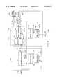
FIG. 3 shows an embodiment of the DLL in more detail. In particular,adjustable delay section 205 comprises a set of four identicaladjustable delay elements 210 connected in series with the output of eachdelay element 210 except the last element connected to the input of thenext element 210. While four delay elements are shown in the particular embodiment, any number such as two, three, four, six, eight or twelve, can be used. This arrangement produces a set of clocks, called phase vectors K<r:0> 270, each shifted in time from the next by a delay, called a unit delay, generated by theadjustable delay section 205. Eachadjustable delay element 210 receives the delay adjustsignal DlyAdj 260 fromcontrol circuit 230, comprisingcounter control circuit 240 and digital-to-analog converter (DAC) 250.Counter control circuit 240 receives an input,PhDiff 225, fromphase detector 220 and generates count Cnt<c:0> 245 for input to the DAC. In one embodiment,control circuit 230 is implemented with digital circuits to permit the storage of the current delay adjustment setting of the loop, held by Cnt<c:0>245, during times when theClkSrc 200 is not present, perhaps during a period when the system is shut down to save power. The saved setting permits the loop to quickly re-acquire a locked condition when the ClkSrc is reactivated.
Continuing with FIG. 3,phase detector 220 receives asinputs ClkIn 215 derived from theClkSrc 200 viabuffer 202 and the last phase vector K<r> 280. In another embodiment,buffer 202 performs duty cycle correction as well as amplification to assure thatClkIn 215 has a 50% duty cycle. Duty cycle correction is discussed in greater detail below.
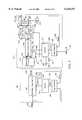
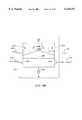
In FIG. 3,adjustable delay element 210 may be implemented according to the embodiment shown in FIG. 16A, which shows adelay element 1010 and abias circuit 1000. In FIG. 16A the delay element is a differential delay element, having both true and complementary inputs and outputs. The circuit operates to delay the differential inputs IN 1005 and IN--B 1015 to produce delayed outputs Out 1130 and Out-- B 1140. The amount of delay is adjusted by adjustablecurrent source 1020, which controls the amount of current switched bydifferential pair Transistors
The adjustable delay element may also be implemented according to the embodiment shown in FIG. 16B. In thisfigure section 1215 functions as a fixed delay comprising acurrent source 1260 and adifferential pair section 1225 operates as a phase interpolator comprisingdifferential pair current source 1320 anddifferential pair current source 1310 to produce a delay that is adjustable between a stage delay to a fixed delay plus the stage delay. The stage delay represents the fixed delay time through theinterpolator stage 1225. The phaseinterpolator delay stage 1225 is adjusted by varying thecurrent sources Ix 1320 andIy 1310. If Ix is at maximum and Iy is turned off the output signals Out 1380 and Out-- B 1370 are produced bytransistors Iy 1310 is maximum andIx 1320 is off then the output signals Out 1380 and Out-- B 1370 are produced bytransistors interpolator delay stage 1225 is adjustable through a range of delay equal to the fixed delay of the 1215 section.
FIG. 3 depicts a DAC which may be implemented according to the DAC shown in FIG. 17, which depicts a circuit for converting a digital count Cnt<c:0> 1510 and its complement Cnt-- B<c:o> 1500 to a differential current pair,Ictl 1640 and Ictl-- B 1590 proportional to the count. FIG. 17 shows three sections of circuitry, a set of binary weightedcurrent sources 1520, a set ofswitches 1540 for producing the truecurrent output Ictl 1640 and a set ofswitches 1530 for producing the complement output Ictl-- B 1590. If the count input Cnt<c:0> 1510 is all ones thenIctl 1640 has a maximum current, Max-- I, which is the sum of all of thecurrent sources adjustable delay element 210 shown in FIG. 16B for the delay-locked loop shown in FIG. 3.
The system shown in FIG. 3 operates as follows.Phase detector 220 compares the ClkIn signal, with the last phase vector K<r> 280 to determine the phase difference from a predetermined phase relationship between the two clocks. In one embodiment the predetermined phase difference could be zero degrees. In another embodiment the predetermined phase difference could be 180 degrees. The phase difference is represented bysignal PhDiff 225. Counter control block then converts the PhDiff signal into a digital count, Cnt<c:0> 245, andDAC 250 converts the count value into an analog quantity,DlyAdj 260, for adjusting the adjustable delay elements. In some embodiments the Cnt<c:0> signal and the DlyAdj signal may be differential signals. The delay adjustment operates to change the delay of the adjustable delay elements so that the phase difference from the predetermined phase relationship between clock input, ClkIn and K<r> is made close to zero. When this condition occurs the DLL is locked, and each adjustable delay element has substantially the same delay. Thus each phase vector is displaced in time from the adjacent vector by an amount equal to the setting of the adjustable delay element. This time displacement is termed a unit delay. The result is that the phase vectors span a 360 degree phase shift of theClkIn signal 215. These phase vectors can now be used in another DLL to lock the phase of an output clock in precise phase relationship to the arbitrary phase of an input clock.
For FIG. 3, an alternate embodiment could use fewer delay elements to produce phase vectors that span the 360 degree phase shift of the ClkIn if each delay element, such as the ones depicted in FIGS. 16A and 16B, can produce both true and complementary outputs. For example, instead of using four delay elements each separated by 90 degrees, two delay elements separated by 90 degrees could be used if the delay element had true outputs yielding delays of 90 and 180 degrees and complementary outputs yielding 270 and 360 degrees, respectively. Alternatively, fewer delay elements could be used if the phase detector were designed to detect phase differences from a predetermined phase relationship of 180 degrees. Using such a phase detector would only require that two delay elements be used spanning a 180 degree phase shift of the ClkIn signal. The outputs of the delay elements could be inverted in a separate circuit which receives the phase vectors, so that a set of phase vectors spanning 360 degrees is obtained. For embodiments in which the phase shift of the ClkIn signal spans only 180 degrees buffer 202 may perform a duty cycle correction function to assure that theClkIn signal 215 has a 50% duty cycle. This is especially important when the remaining span of 180 degrees is derived through inversion of the phase vectors spanning the first 180 degrees, because inversion will not generate the proper phase shift if the duty cycle is not substantially close to 50%.
Referring the embodiment in FIG. 4, an additional adjustable delay element has been placed in the circuit to receive the last phase vector. This additional delay has the effect of insuring that each phase vector has the identical loading as the other phase vectors, so that phase errors caused by loading differences are substantially eliminated. Rather than connecting the delay adjustsignal 265 to theDlyAdj signal 260, signal 265 may be connected to a convenient voltage, because the output of the additional delay is not used. This eliminates some of the loading on theDlyAdj signal 260.
Continuing with the embodiment of FIG. 4,phase vectors 275 are buffered bybuffers 212 in order to further control the loading on the vectors by isolating the loading of the phase vectors from other circuits which may receive the vectors. A buffered version ofClkIn 215 and a buffered version of the last phase vector K<r> 285 are sent to the phase detector. This guarantees that buffered version of the phase vectors K<r:0> 275 are separated in phase by a unit delay and that the set of buffered phase vectors span a 360 degree or 180 degree shift of the buffered ClkIn signal depending upon the embodiment chosen.
Also shown in FIG. 4 is a version ofbuffer 202 which has a dutycycle correcting circuit 290 attached. The dutycycle correcting circuit 290 senses signal 214 for a deviation from a 50% duty cycle. It then feeds a correction signal to buffer 202 to correctsignal 214. In some embodiments signal 214 is a differential signal and theerror signal 295 is a differential signal.
An embodiment of a duty cycle correcting amplifier is shown in FIGS. 19A and 19B. FIG. 19A shows the correctingstage 2005 and thebuffering stage 2055 and FIG. 19B shows the duty cycleerror detecting stage 2215. In FIG. 19Adifferential pair In+ 1920 and In- 1930 and produce a differential output clock on Corr Clock-- B 2090 andCorr Clock 2100. If the duty cycle deviates from 50% then the circuit shown in FIG. 19B will produce a differential error voltagesignal pair Error+ 2300 and Error- 2200 from thedifferential pair capacitor 2260 acting as an integrator.Transistors capacitor 2260. The differential error voltage signal pair is fed back to the correctingstage 2005 such that the duty cycle error in the Corr Clock and Corr Clock-- B signals is reduced by alteringcurrents buffering stage 2055 is a clock having a duty cycle substantially close to 50%.
In FIG. 4, as in FIG. 3,Phase detector 220 compares the ClkIn signal, with the last phase vector K<r> 280 to determine the phase difference from a predetermined phase relationship between the two clocks, and signalPhDiff 225 represents that difference. In FIG. 3, PhDiff signal 225 contains random variations due to the instantaneous phase error which, when used directly byCounter Control 240, causes an amount of overall loop jitter, thus affecting the stability of the phase vectors. In FIG. 4, the amount of jitter is reduced by filtering the PhDiff signal before converting it to DlyAdj signal 260. Shown in FIG. 4 is an embodiment in whichcontrol circuit 230 includesfilter 235 in addition tocounter control 240 and digital to analog converter (DAC) 250.Filter circuit 235 receives an input,PhDiff 225, fromphase detector 220 andCntClk 241 frombuffer 238 and generatesoutput PhDiffF 237 for input to theCounter Control 240, which receivesCntClk 241 and generates count Cnt<c:0> 245 for input toDAC 250. In an embodiment in which the PhDiff signal is a digital signal, a digital filter is used, but either analog or digital filtering may be employed.CntClk 241 operates the circuitry in bothFilter 235 andCounter Control 240.Buffer 238 is employed when ClkSrc is a small swing signal butCounter Control 240 and Filter 235 require a full swing signal.
Types of digital filters that can be employed to reduce loop jitter include a majority-detector filter or an unanimity-detector filter. In either filter type,CntClk 241 operates circuitry which samples and stores the state, either true or false, ofPhDiff 225. A majority-detector filter saves the last N samples, where N is an odd number, ofPhDiff signal 225 and determines whether a majority of the last N cycles, say 3 out of 5 (N), are the same. If so, then the majority-detector filter activatesPhDiffF 237 to alter the count incounter control 240. This type of filter alters the count incounter control 240 on every sample because there is always a majority of true or false samples. An unanimity-detector filter also records the last N samples, where N can be even or odd, of the PhDiff signal but instead determines whether all N cycles are the same. If all samples are the same, the unanimity-detector filter activates thePhDiffF signal 237 to alter the count and at times during which not all the samples are the same, the PhDiffF signal will not be activated to alter the count. Both types of filters have the effect of reducing loop jitter, and either type may be used.
Turning now to FIG. 5, a pair of delay-locked loops is depicted for generating an output clock having a predetermined phase relationship to an input clock. The first delay-lockedloop 320 is one which generates phase vectors K<r:0> 330 from aclock source ClkSrc 300 as described above. The phase vectors and theDlyAdj signal 340 are then used by a second delay-lockedloop 350 to create a precise phase relationship betweenInput Clock 310 andOutput Clock 360.
FIG. 6 shows an embodiment of the loop of FIG. 5 in more detail.First loop 400 is the phase vector loop which receivesClkSrc 410 and generates phase vectors K<r:0> 430 andDlyAdj signal 440. Thesecond loop 500 is the loop for creating the phase relationship between theInput Clk 650 andOutput Clk 640.Loop 500 comprises aselection circuitry 510,phase interpolator 560,adjustable delay section 610 which represents an integer multiple of adjustable delay elements, clock buffers 620 and 630,control circuit 570 andphase detector 590.
In FIG. 6,selection circuitry 510 receives thephase vectors 430 and passes along a selected pair ofvectors Kx 520 andKy 530, which are received byphase interpolator 560. The phase interpolator generates an interpolatedoutput clock 615 which is buffered byclock buffer 620 to become theOutput Clk 640.
The operation of the circuit of FIG. 18 is substantially similar to the circuit shown in FIG. 16B.Differential pair Differential pair capacitors C1 1760 andC2 1770 andcoincidence detector 1860. IfIctl 1720 is set at a maximum value and Ictl-- B 1730 is zero then theoutput signal PIout 1870 is in phase with the Kx clock but delayed by a stage delay through the interpolator. If Ictl-- B 1730 is set a maximum value andIctl 1720 is zero then the output signal is in phase with the Ky clock but delayed by a stage delay. By adjusting the values ofadjustable currents
The operation ofloop 500 in FIG. 6 is as follows.Phase detector 590 determines what the difference in phase, if any, is between theInput Clk 650 andFdBkClk 600. This difference is then processed bycontrol circuit 570 to select a pair of phase vectors viaselection circuitry 510. The chosen pair of vectors is that pair between which the phase ofInput Clk 650 lies, after accounting for fixed delays inherent in circuits in the path of the FdBkClk signal such as the phase selector, phase interpolator, adjustable delay section and clock buffer. An example of a pair of vectors meeting this requirement is shown in FIG. 14, in which the Input Clk is shown between the 90 degree and 180 degree vectors and at a delay of alpha degrees from the 180 degree vector. If the starting pair of vectors is not the correct pair then the control circuit steps through the pairs of vectors one step at a time until the correct pair is discovered. FIG. 15 depicts a circumstance in which the stepping of several phase vectors must occur ifloop 500 starts in the 0 degree state before the correct pair is discovered. When the first pair of vectors, 0 and 45 degrees, is selected, thephase interpolator 560 is adjusted so that thephase interpolator output 615 is in phase with the 45 degree vector. While in this condition the 0 degree vector is replaced with the 90 degree vector by the control circuit and selection circuitry. Next, the phase interpolator is adjusted to produce an output in phase with the 90 degree vector and the 45 degree vector is replaced with the 135 degree vector. The phase interpolator is then adjusted to produce an output in phase with the 135 degree vector. Finally, the control circuit replaces the 90 degree vector with the 180 degree vector. Thus, while this stepping occurs the phase interpolator generates anoutput clock 615 which is in phase with one of the selected vectors, in particular, the one that will not be switched in selecting a new pair of vectors. The constraint that the interpolator generate the output clock in phase with the non-switched vector prevents the output clock from glitching during the stepping process. When the correct pair of vectors is determined by the loop then the phase interpolator is allowed to be adjusted byPhAdj signal 550 to precisely align the delayedoutput FdBkClk 600 to the phase of theInput Clk 650, which is at some phase, alpha degrees, (FIG. 14) from one of the selected phase vectors. When this occurs the loop is locked.FdBkClk 600 is delayed by at least one unit delay fromadjustable delay section 610, the unit delay being precisely a delay between any twoadjacent phase vectors 430 from the first loop because it is adjusted by thesame DlyAdj 440 signal of the first loop. Thus, if the phase vectors from the first loop differ from each other by 90 degrees, then the unit delay is 90 degrees and the FdBkClk is delayed 90 degrees from the output of thephase interpolator 615, assuming one delay element inblock 610. FIG. 14 shows this condition.
It will be noted that not only is a unit delay included in the feedback path of the second loop but so are the clock buffer and other fixed delays inherent in the phase selector and phase interpolator. Clock buffers 620 and 630 are matched buffers having the same physical construction. FdBkClk is thus delayed by an amount equal to a unit delay and a clock buffer delay plus the other fixed delays from the phase selector and phase interpolator. However, because theOutput Clk 640 is delayed by the same amount of fixed delays, the clock buffer delays and fixed delays cancel and the difference between the Output Clk 640 and theInput Clock 650 is only the unit delay.
It should be noted thatadjustable delay section 610 could comprise an integer multiple of unit delays, in which case the delay between theInput Clk 650 andOutput Clk 640 would then be the integer multiple of unit delays. For example, if the multiple of the unit delay is 3 and the value of the unit delay 10 degrees then the Output Clk would lead the Input Clk by 30 degrees. If the multiple of the unit delay is zero, then the Input Clk and Output Clk would be in phase.
FIG. 7 is an alternate embodiment showingadjustable delay section 612 in the path of theOutput Clk 640. This section has the same implementation as the section in the path of theFdBkClk 600 and provides a way for theOutput Clk 640 to not only lead the Input Clk in phase but to lag it in phase. This latter condition occurs when theadjustable delay section 612 comprises a larger multiple of unit delays thanadjustable delay section 610.Adjustable delay sections section 206 in FIG. 4 in order to insure that phase errors due to loading differences are minimized. The delay circuits shown in FIGS. 16A and 16B are suitable for implementing an adjustable delay element employed in theadjustable delay section buffers cycle correction circuit 670.Buffers cycle correction circuit 670 may be implemented as shown in FIG. 19B. Finally, FIG. 7 shows three more inputs,Fast 575,Test 585 andExtIn 595, to thecontrol circuit 570. In one embodimentFast signal 575 is used to alter the control circuit so that the loop can lock more quickly by taking larger phase adjustments toward the lock condition. In an embodiment in which thecontrol circuit 570 is implemented as a counter, theFast signal 575 can cause the counter to count by a multiple of the smallest step between counts. TheTest signal 585 is used to allow the control circuit to be under the control ofexternal signal ExtIn 595 rather thanPhDiff 580 derived from the loop. This allows loop properties to be tested more easily.
FIG. 8 shows one embodiment ofadjustable delay section 612.Block 612 comprises abuffer 702, similar to 202 in FIG. 4, anadjustable delay element 710 similar toadjustable delay element 210 in FIG. 4, and anoutput buffer 712 similar to the 212 buffer in FIG. 4. FIG. 9 shows an embodiment ofadjustable delay section 610. This figure is similar to FIG. 8 but has more adjustable delay elements, but is still buffered at the front of the chain and has an additional delay element at the end of the chain. The adjustable delay sections in both FIG. 8 and FIG. 9 are controlled from an external delay adjust signal such as 441 as shown in FIG. 7, such that the setting produces a delay equal to the delay between phase vectors. If the adjustable delay sections are implemented in this fashion, loading differences are kept to a minimum and only the desired phase difference betweensignal adjustable delay sections same section 625 as shown in FIG. 7 and 10. The delay adjustsignal 441 in FIG. 7 is buffered bybuffer 442, in some embodiments, to isolate the loading effects ofsections section 420.
FIG. 20 discloses circuitry for biasing the predetermined phase relationship between the input clock and the output clock with a fixed offset. The fixed offset is necessary when system requirements dictate that the predetermined phase relationship be altered by an amount that is smaller than is available from a unit a delay, for example a one degree phase shift. This fine tuning or trimming is accomplished by theTrimAdj signal 2300 which is combined with theDlyAdj signal 441 in FIG. 7. TheTrimAdj signal 2300 adds a small amount of adjustment current to theadjustable delay sections TrimAdj signal 2300 is derived fromDAC 2310 and trimword storage 2320. Trim word storage in some embodiments is a set of fuses or other permanent storage for holding a digital code TW<t:0> 2330 for setting the trim delay.DAC 2310 converts thetrim word 2330 to an analog signal such as a current for controlling the delay elements insections
FIG. 21 is a circuit diagram of a phase detector circuit which could be used for the phase detector of FIGS. 2, 3, 4, 6 and 7. Aclock input 2530 is shown, anddata input 2540 would correspond to the feedback clock or phase vector.Output 3000 is the phase difference signal provided to the control circuit. The phase detector is implemented as threeblocks NAND gates
FIG. 22 shows a system application for the delay-locked loops of the present invention. In the case shown,master device 3100 communicates withslave device 3110 orslave device 3120.Slave devices master device 3100 but not with each other. The system operates from a pair of clocks generated fromoscillator 3170 which generates CTM (Clock To Master) 3140 and CFM (Clock From Master) 3130. CTM travels in the direction from the slave device to the master device and is used for transmitting data to the master ondata bus 3150. In the master, CTM is looped back to generate CFM which travels in the direction from master to slave device and is used for transmitting data from the master to the slave device. Each device, master or slave, has adata receiver Rcvr 3180 and adata transmitter Txmtr 3190 for receiving and sending data respectively. TheRcvr 3180 uses asignal rclk 3220 to receive the data from the data Bus andTxmtr 3190 uses tclk 3230 to transmit the data onto the data bus. Signals rclk and tclk are generated from a pair of delay-lockedloops loop 3235 in the master, because the master makes no distinction between CTM and CFM.
In FIG. 22DLLR 3210 is the delay-locked loop for generating the phase vectors and is called the reference loop. Each device uses a single DLLR loop.DLLF 3200 is the delay-locked loop for generating a predetermined phase relationship between the input clock and the output clock. TheDLLF 3200 loop is used to generate a 90 degree phase relationship between CTM and tclk, because data is always transmitted in quadrature to the receive clock. TheDLLF 3205 is used to generate a zero degree phase relationship between CFM and rclk. Thus, when a slave sends data to the master, the data changes occur 90 degrees out of phase with the CTM clock, the clock traveling toward the master. The master receives the clock CTM and generates the rclk signal for operating its receiver. Signal rclk in the master is in a 0 degree phase relationship with CTM so that the data is sampled when it is not changing. Similarly, when the master sends data to a slave, it clocks its transmitter changing the data on the data bus with tclk which is in a 90 degree phase relationship with the CFM. Aslave 3110 receiving the data in itsreceiver 3180 operates its receiver using rclk which has a 0 degree phase relationship with the CFM. Thus, the receiver will sample the data when it is not changing. In this manner, data may be transmitted using both edges of the CTM or CFM clocks and safely sampled in the receiver.
In one embodiment, the master of FIG. 22 is an intelligent device, such as a microprocessor, an application specific integrated circuit (ASIC), a memory controller, or a graphics engine. The slave devices may be DRAMs, SRAMs, ROMs, EPROMs, flash memories, or other memory devices.
In the foregoing specification the invention has been described with reference to specific exemplary embodiments thereof. It will, however, be evident that various modifications and changes may be made thereto without departing from the broader spirit and scope of the invention. The specification and drawings are, accordingly, to be regarded in an illustrative rather than restrictive sense.
Claims (20)
1. A method for generating an output clock with a predetermined phase relationship with an input clock, the method comprising the steps of:
selecting a pair of adjacent phase vectors from a set of phase vectors, each vector separated in time from an adjacent vector by a unit delay;
generating the output clock using an interpolator that receives the selected pair of phase vectors;
delaying the output clock from the interpolator by a delay equal to a multiple of the unit delay to produce a feedback clock;
adjusting the selection of a pair of adjacent phase vectors received by the interpolator so that the phase of the input clock lies between the selected pair of phase vectors;
detecting the difference in phase between the input clock and the feedback clock;
interpolating between the selected pair of adjacent phase vectors using the interpolator so that the feedback clock is in phase with the input clock based on the detected phase difference between the input clock and the feedback clock; and
wherein the output clock from the interpolator has the predetermined phase relationship with the input clock when the feedback clock is in phase with the input clock, the predetermined phase relationship being a multiple of the unit delay.
2. The method of claim 1, wherein the step of detecting the difference in phase includes the step of filtering the detected phase difference between the input clock and the feedback clock.
3. The method of claim 1, further comprising the step of storing the current selection of phase vectors and the current adjustment of the interpolator, wherein the current selection of phase vectors and the current adjustment of the interpolator are preserved during a period of time when the input clock not is not present or the set of phase vectors is not present.
4. The method of claim 1, wherein the multiple of the unit delay includes zero.
5. The method of claim 1, further comprising the step of delaying the output clock from the interpolator by a delay equal to a multiple of the unit delay to produce the output clock, wherein the output clock has a predetermined phase relationship with the input clock, the predetermined phase relationship being a multiple of the unit delay.
6. The method of claim 5, wherein the output clock may lead or lag the input clock by a multiple of the unit delay.
7. The method of claim 1, wherein the output clock from the interpolator is buffered with a first clock buffer to produce the output clock; and
wherein the feedback clock is buffered with a second clock buffer to produce the feedback clock, the first and second clock buffers having substantially the same delay and the output clock having a predetermined phase relationship with the input clock, the predetermined phase relationship being a multiple of the unit delay.
8. Circuitry for generating an output clock having a predetermined phase relationship with an input clock, the circuitry comprising:
selection circuitry having as inputs a set of phase vectors and a selection control signal, each vector separated in time from an adjacent vector by a unit delay, the selection circuitry for selecting a pair of adjacent phase vectors from the set;
a phase interpolator circuit receiving the selected pair of adjacent phase vectors and a phase adjust signal and generating the output clock, the phase interpolator for adjusting the phase of the output clock;
at least one feedback delay element coupled to the output clock to produce a feedback clock, the feedback delay element delaying the feedback clock from the output clock by an amount equal to a multiple of the unit delay; and
a phase adjusting circuit receiving the input clock and the feedback clock, wherein the phase adjusting circuit produces the selection control signal for adjusting the selection of a pair of adjacent phase vectors produced by the selection circuitry so that the phase of the input clock lies between the selected pair of adjacent phase vectors and wherein the phase adjusting circuit produces the phase adjust signal for adjusting the phase interpolator so that the feedback clock is in phase with the input clock, wherein the output clock has the predetermined phase relationship with the input clock when the feedback clock is in phase with the input clock, the predetermined phase relationship being a multiple of the unit delay.
9. The circuitry of claim 8, wherein the multiple of the unit delay includes zero.
10. The circuitry of claim 8, wherein the output clock from the phase interpolator is buffered with a first clock buffer to produce the output clock and wherein the feedback clock is buffered with a second clock buffer to produce the feedback clock, the first and second clock buffers having substantially the same delay and the output clock having a predetermined phase relationship with the input clock, the predetermined phase relationship being a multiple of the unit delay.
11. The circuitry of claim 8, wherein the phase adjusting circuit comprises:
a phase detector receiving the input clock and the feedback clock, the phase detector for determining whether the feedback clock is in phase with the input clock and for producing a phase detector output based on the difference in phase between the feedback clock and the input clock; and
a control circuit receiving the phase detector output signal, the control circuit producing the selection control signal for adjusting the selection of a pair of phase vectors generated by the selection circuitry and producing the phase adjust signal for adjusting the phase interpolator.
12. The circuitry of claim 11, wherein the control circuit includes a digital storage circuit having state information for representing the currents election of phase vectors and the adjustment of the phase interpolator.
13. The circuitry of claim 12, wherein the state information of the digital storage circuit is preserved when the input clock not is not present or the set of phase vectors is not present.
14. The circuitry of claim 11, wherein the control circuit includes:
a counter circuit receiving the phase detector output signal and generating a digital count based on the phase detector output signal; and
a digital-to-analog converter receiving the digital count and generating the phase adjust signal, wherein the phase adjust signal is an analog signal proportional to the digital count.
15. The circuitry of claim 11, wherein the control circuit includes:
a filter receiving the phase detector output signal and generating a filtered phase detector output signal for reducing loop jitter;
a counter circuit receiving the filtered phase detector output signal and generating a digital count based on the phase detector output signal; and
a digital-to-analog converter receiving the digital count and generating the phase adjust signal, wherein the phase adjust signal is an analog signal proportional to the digital count.
16. The circuitry of claim 15, wherein the filter is a digital filter.
17. The circuitry of claim 8, further comprising:
a first duty cycle correcting amplifier receiving the feedback clock;
a second duty cycle correcting amplifier receiving the output clock; and
a duty cycle correcting circuit receiving the feedback clock and adjusting the first and second duty cycle correcting amplifiers such that the feedback clock and output clock have substantially the same duty cycle, wherein the duty cycle is substantially close to 50%.
18. Circuitry for generating an output clock signal having a predetermined phase relationship with an input clock signal, the circuitry comprising:
selection circuitry having as inputs a set of phase vector signals and a selection control signal, each phase vector signal separated in time from an adjacent phase vector signal by a unit delay, the selection circuitry for selecting a pair of adjacent phase vector signals from the set;
a phase interpolator circuit receiving the selected pair of adjacent phase vector signals and a phase adjust signal and generating a phase interpolator output clock signal, the phase interpolator circuit adjusting the phase of the phase interpolator output clock;
at least one output delay element to receive the phase interpolator output clock signal and to produce the output clock signal, the output delay element delaying the phase interpolator output clock signal by an amount equal to a multiple of the unit delay; and
a phase adjusting circuit receiving the input clock signal and the phase interpolator output clock signal, wherein the phase adjusting circuit produces the selection control signal for adjusting the selection of a pair of adjacent phase vector signals produced by the selection circuitry so that the phase of the input clock signal lies between the selected pair of adjacent phase vector signals and wherein the phase adjusting circuit produces the phase adjust signal for adjusting the phase interpolator so that the phase interpolator output clock signal is in phase with the input clock signal, wherein the output clock signal has the predetermined phase relationship with the input clock signal when the phase interpolator output clock signal is in phase with the input clock signal, the predetermined phase relationship being a multiple of the unit delay.
19. The circuitry of claim 18 further comprising:
at least one feedback delay element coupled to the phase adjusting circuit for delaying the phase interpolator output clock signal by an amount equal to a multiple of the unit delay.
20. The circuitry of claim 19, wherein the output clock signal may lead or lag the input clock signal by a multiple of the unit delay.
Priority Applications (11)
| Application Number | Priority Date | Filing Date | Title |
|---|---|---|---|
| US08/795,657US6125157A (en) | 1997-02-06 | 1997-02-06 | Delay-locked loop circuitry for clock delay adjustment |
| DE29825196UDE29825196U1 (en) | 1997-02-06 | 1998-02-04 | Circuit for setting a clock delay |
| DE69840242TDE69840242D1 (en) | 1997-02-06 | 1998-02-04 | Delay loop circuit for setting a clock delay |
| EP05018741AEP1601130B1 (en) | 1997-02-06 | 1998-02-04 | Delay locked loop circuitry for clock delay adjustment |
| PCT/US1998/002053WO1998037656A2 (en) | 1997-02-06 | 1998-02-04 | Delay locked loop circuitry for clock delay adjustment |
| DE69840350TDE69840350D1 (en) | 1997-02-06 | 1998-02-04 | Circuit with delay locked loop to adjust the clock delay |
| EP98906112AEP1031203A4 (en) | 1997-02-06 | 1998-02-04 | Delay locked loop circuitry for clock delay adjustment |
| EP05025847AEP1633049B1 (en) | 1997-02-06 | 1998-02-04 | Delay locked loop circuitry for clock delay adjustment |
| US09/524,402US6539072B1 (en) | 1997-02-06 | 2000-03-13 | Delay locked loop circuitry for clock delay adjustment |
| US10/366,865US7039147B2 (en) | 1997-02-06 | 2003-02-14 | Delay locked loop circuitry for clock delay adjustment |
| US11/406,557US7308065B2 (en) | 1997-02-06 | 2006-04-18 | Delay locked loop circuitry for clock delay adjustment |
Applications Claiming Priority (1)
| Application Number | Priority Date | Filing Date | Title |
|---|---|---|---|
| US08/795,657US6125157A (en) | 1997-02-06 | 1997-02-06 | Delay-locked loop circuitry for clock delay adjustment |
Related Child Applications (1)
| Application Number | Title | Priority Date | Filing Date |
|---|---|---|---|
| US09/524,402ContinuationUS6539072B1 (en) | 1997-02-06 | 2000-03-13 | Delay locked loop circuitry for clock delay adjustment |
Publications (1)
| Publication Number | Publication Date |
|---|---|
| US6125157Atrue US6125157A (en) | 2000-09-26 |
Family
ID=25166104
Family Applications (4)
| Application Number | Title | Priority Date | Filing Date |
|---|---|---|---|
| US08/795,657Expired - LifetimeUS6125157A (en) | 1997-02-06 | 1997-02-06 | Delay-locked loop circuitry for clock delay adjustment |
| US09/524,402Expired - LifetimeUS6539072B1 (en) | 1997-02-06 | 2000-03-13 | Delay locked loop circuitry for clock delay adjustment |
| US10/366,865Expired - Fee RelatedUS7039147B2 (en) | 1997-02-06 | 2003-02-14 | Delay locked loop circuitry for clock delay adjustment |
| US11/406,557Expired - Fee RelatedUS7308065B2 (en) | 1997-02-06 | 2006-04-18 | Delay locked loop circuitry for clock delay adjustment |
Family Applications After (3)
| Application Number | Title | Priority Date | Filing Date |
|---|---|---|---|
| US09/524,402Expired - LifetimeUS6539072B1 (en) | 1997-02-06 | 2000-03-13 | Delay locked loop circuitry for clock delay adjustment |
| US10/366,865Expired - Fee RelatedUS7039147B2 (en) | 1997-02-06 | 2003-02-14 | Delay locked loop circuitry for clock delay adjustment |
| US11/406,557Expired - Fee RelatedUS7308065B2 (en) | 1997-02-06 | 2006-04-18 | Delay locked loop circuitry for clock delay adjustment |
Country Status (4)
| Country | Link |
|---|---|
| US (4) | US6125157A (en) |
| EP (3) | EP1601130B1 (en) |
| DE (3) | DE69840350D1 (en) |
| WO (1) | WO1998037656A2 (en) |
Cited By (169)
| Publication number | Priority date | Publication date | Assignee | Title |
|---|---|---|---|---|
| US20010018751A1 (en)* | 2000-02-28 | 2001-08-30 | Gresham Paul Alan | Integrated data clock extractor |
| US6304117B1 (en)* | 1997-07-29 | 2001-10-16 | Fujitsu Limited | Variable delay circuit and semiconductor integrated circuit device |
| US6342797B1 (en)* | 1998-12-30 | 2002-01-29 | Hyundai Electronics Industries Co., Ltd. | Delayed locked loop clock generator using delay-pulse-delay conversion |
| US6369652B1 (en) | 2000-05-15 | 2002-04-09 | Rambus Inc. | Differential amplifiers with current and resistance compensation elements for balanced output |
| US6373301B1 (en) | 2001-04-18 | 2002-04-16 | Silicon Integrated Systems Corporation | Fast-locking dual rail digital delayed locked loop |
| US6388482B1 (en)* | 2000-06-21 | 2002-05-14 | Infineon Technologies North America Corp. | DLL lock scheme with multiple phase detection |
| US6392466B1 (en)* | 1999-12-30 | 2002-05-21 | Intel Corporation | Apparatus, method and system for a controllable pulse clock delay arrangement to control functional race margins in a logic data path |
| US6400197B2 (en)* | 2000-01-26 | 2002-06-04 | Via Technologies, Inc. | Delay device having a delay lock loop and method of calibration thereof |
| US20020070752A1 (en)* | 2000-08-30 | 2002-06-13 | Harrison Ronnie M. | Method and system for controlling the duty cycle of a clock signal |
| US6424184B1 (en)* | 1996-09-25 | 2002-07-23 | Matsushita Electric Industrial Co., Ltd. | Frequency-voltage conversion circuit, delay amount judgement circuit, system having frequency-voltage conversion circuit, method of adjusting input/output characteristics of frequency-voltage conversion circuit, and apparatus for automatically adjusting input |
| US6434706B1 (en)* | 1999-05-24 | 2002-08-13 | Koninklijke Philips Electronics N.V. | Clock system for multiple component system including module clocks for safety margin of data transfers among processing modules |
| US6441662B2 (en)* | 2000-05-30 | 2002-08-27 | Mitsubishi Denki Kabushiki Kaisha | DLL circuit that can prevent erroneous operation |
| US6445234B1 (en)* | 1998-12-30 | 2002-09-03 | Hyundai Electronics Industries Co., Ltd. | Apparatus and method for accelerating initial lock time of delayed locked loop |
| US6452431B1 (en)* | 2000-08-28 | 2002-09-17 | Micron Technology, Inc. | Scheme for delay locked loop reset protection |
| US6456130B1 (en)* | 2001-01-11 | 2002-09-24 | Infineon Technologies Ag | Delay lock loop and update method with limited drift and improved power savings |
| US20020140472A1 (en)* | 2001-03-27 | 2002-10-03 | Hiroshi Sonobe | Semiconductor device |
| US20020154723A1 (en)* | 2001-01-11 | 2002-10-24 | Nec Corporation | Oversampling clock recovery having a high follow-up character using a few clock signals |
| WO2002087086A1 (en)* | 2001-04-19 | 2002-10-31 | Micron Technology, Inc. | Clock generator using master and slave dlls |
| US20020163986A1 (en)* | 1999-03-01 | 2002-11-07 | Harrison Ronnie M. | Method and apparatus for generating a phase dependent control signal |
| EP1265247A1 (en)* | 2001-06-05 | 2002-12-11 | STMicroelectronics S.r.l. | A programmable delay line and corresponding memory |
| US20020196885A1 (en)* | 2001-06-25 | 2002-12-26 | Jun Kim | Determining phase relationships using digital phase values |
| US6501313B2 (en)* | 2000-12-27 | 2002-12-31 | International Business Machines Corporation | Dynamic duty cycle adjuster |
| US20030012321A1 (en)* | 2001-07-12 | 2003-01-16 | Mitsubishi Denki Kabushiki Kaisha | Delay locked loop circuit and its control method |
| US6518811B1 (en) | 2000-12-29 | 2003-02-11 | Cisco Technology, Inc. | Software programmable delay circuit |
| US6525581B1 (en) | 2001-09-20 | 2003-02-25 | Hynix Semiconductor Inc. | Duty correction circuit and a method of correcting a duty |
| US6530006B1 (en) | 2000-09-18 | 2003-03-04 | Intel Corporation | System and method for providing reliable transmission in a buffered memory system |
| US20030052718A1 (en)* | 2001-09-19 | 2003-03-20 | Elpida Memory, Inc. | Interpolating circuit, DLL circuit and semiconductor integrated circuit |
| US6549046B1 (en)* | 2000-12-29 | 2003-04-15 | Cisco Technology, Inc. | Method and apparatus for phase aligning two clock signals utilizing a programmable phase adjustment circuit |
| US6570944B2 (en) | 2001-06-25 | 2003-05-27 | Rambus Inc. | Apparatus for data recovery in a synchronous chip-to-chip system |
| US6583655B2 (en)* | 2001-05-24 | 2003-06-24 | Nec Electronics Corporation | Clock control circuit |
| US20030117864A1 (en)* | 2001-10-22 | 2003-06-26 | Hampel Craig E. | Phase adjustment apparatus and method for a memory device signaling system |
| US20030117194A1 (en)* | 2001-12-21 | 2003-06-26 | Lee Seong Hoon | Delay locked loop circuit with duty cycle correction function |
| US20030123594A1 (en)* | 2002-01-02 | 2003-07-03 | Glenn Robert C. | Phase interpolator based clock recovering |
| US6597212B1 (en) | 2002-03-12 | 2003-07-22 | Neoaxiom Corporation | Divide-by-N differential phase interpolator |
| US20030161430A1 (en)* | 2002-02-26 | 2003-08-28 | Fujitsu Limited | Clock recovery circuitry |
| US6621762B1 (en)* | 2002-05-29 | 2003-09-16 | Micron Technology, Inc. | Non-volatile delay register |
| US20030179027A1 (en)* | 2002-03-22 | 2003-09-25 | Kizer Jade M. | Locked loop with dual rail regulation |
| US20030183842A1 (en)* | 2002-03-22 | 2003-10-02 | Kizer Jade M. | System with phase jumping locked loop circuit |
| US6636098B1 (en) | 2001-12-05 | 2003-10-21 | Rambus Inc. | Differential integrator and related circuitry |
| US6642760B1 (en) | 2002-03-29 | 2003-11-04 | Rambus, Inc. | Apparatus and method for a digital delay locked loop |
| WO2002031980A3 (en)* | 2000-10-13 | 2003-11-06 | Silicon Comm Lab Inc | Cyclic phase signal generation from a single clock source using current phase interpolation |
| US6650157B2 (en)* | 2002-01-11 | 2003-11-18 | Sun Microsystems, Inc. | Using a push/pull buffer to improve delay locked loop performance |
| US20030219089A1 (en)* | 2002-05-21 | 2003-11-27 | Via Technologies, Inc. | Delay phase-locked loop device and clock signal generating method |
| US6665219B2 (en)* | 2001-02-12 | 2003-12-16 | Micron Technology, Inc. | Method of reducing standby current during power down mode |
| US20040008733A1 (en)* | 2002-07-12 | 2004-01-15 | Berthold Wedding | Multiplexer input circuit with DLL phase detector |
| US20040012429A1 (en)* | 2000-12-05 | 2004-01-22 | Mikael Lindberg | Device and method in a semiconductor circuit |
| US6686785B2 (en)* | 2001-10-11 | 2004-02-03 | Sun Microsystems, Inc. | Deskewing global clock skew using localized DLLs |
| US6687881B2 (en)* | 2002-02-14 | 2004-02-03 | Sun Microsystems, Inc. | Method for optimizing loop bandwidth in delay locked loops |
| WO2002097987A3 (en)* | 2001-05-25 | 2004-02-19 | Infineon Technologies Ag | Method and system for managing a pulse width of a signal pulse |
| US20040041604A1 (en)* | 2002-09-03 | 2004-03-04 | Kizer Jade M. | Phase jumping locked loop circuit |
| US20040052323A1 (en)* | 2002-09-13 | 2004-03-18 | Bo Zhang | Phase interpolater and applications thereof |
| US20040066873A1 (en)* | 2002-10-05 | 2004-04-08 | Cho Geun-Hee | Delay locked loop circuit for internally correcting duty cycle and duty cycle correction method thereof |
| US6727738B2 (en)* | 2000-12-19 | 2004-04-27 | Renesas Technology Corp. | Configuration for generating a clock including a delay circuit and method thereof |
| US20040101079A1 (en)* | 2002-11-25 | 2004-05-27 | International Business Machines Corporation | Delay-lock-loop with improved accuracy and range |
| US20040140837A1 (en)* | 2003-01-21 | 2004-07-22 | Altera Corporation | Digital phase locked loop circuitry and methods |
| US6775342B1 (en) | 1998-06-22 | 2004-08-10 | Xilinx, Inc. | Digital phase shifter |
| US20040155686A1 (en)* | 2003-01-10 | 2004-08-12 | Se-Jun Kim | Analog delay locked loop having duty cycle correction circuit |
| US20040179419A1 (en)* | 2003-03-12 | 2004-09-16 | Choi Joo S. | Multi-frequency synchronizing clock signal generator |
| US6794919B1 (en) | 2000-09-29 | 2004-09-21 | Intel Corporation | Devices and methods for automatically producing a clock signal that follows the master clock signal |
| US6806750B1 (en)* | 2002-04-23 | 2004-10-19 | National Semiconductor Corporation | Method and system for clock deskewing using a continuously calibrated delay element in a phase-locked loop |
| US20040223571A1 (en)* | 1997-02-06 | 2004-11-11 | Rambus Inc. | Delay locked loop circuitry for clock delay adjustment |
| EP1497923A1 (en)* | 2002-03-22 | 2005-01-19 | Rambus, Inc. | System with dual rail regulated locked loop |
| US6856558B1 (en) | 2002-09-20 | 2005-02-15 | Integrated Device Technology, Inc. | Integrated circuit devices having high precision digital delay lines therein |
| US20050046453A1 (en)* | 2003-09-03 | 2005-03-03 | Broadcom Corporation | Method and apparatus for glitch-free control of a delay-locked loop in a network device |
| US20050053162A1 (en)* | 2001-11-20 | 2005-03-10 | Masaru Goishi | Phase adjustment apparatus and semiconductor test apparatus |
| US6867627B1 (en) | 2003-09-16 | 2005-03-15 | Integrated Device Technology, Inc. | Delay-locked loop (DLL) integrated circuits having high bandwidth and reliable locking characteristics |
| US20050083721A1 (en)* | 2001-09-07 | 2005-04-21 | Hampel Craig E. | Granularity memory column access |
| US20050088211A1 (en)* | 2003-10-24 | 2005-04-28 | Kim Kyu-Hyoun | Jitter suppressing delay locked loop circuits and related methods |
| US6889304B2 (en) | 2001-02-28 | 2005-05-03 | Rambus Inc. | Memory device supporting a dynamically configurable core organization |
| US6897699B1 (en) | 2002-07-19 | 2005-05-24 | Rambus Inc. | Clock distribution network with process, supply-voltage, and temperature compensation |
| WO2005057718A1 (en)* | 2003-12-10 | 2005-06-23 | Telefonaktiebolaget Lm Ericsson (Publ) | A delay-locked loop with precision controlled delay |
| WO2005064434A1 (en)* | 2003-12-19 | 2005-07-14 | Koninklijke Philips Electronics N.V. | Integrated circuit clock distribution |
| US6922091B2 (en) | 2002-09-03 | 2005-07-26 | Rambus Inc. | Locked loop circuit with clock hold function |
| US20050220235A1 (en)* | 2000-02-07 | 2005-10-06 | Stark Donald C | System and method for aligning internal transmit and receive clocks |
| US6954097B2 (en)* | 1997-06-20 | 2005-10-11 | Micron Technology, Inc. | Method and apparatus for generating a sequence of clock signals |
| US20050237093A1 (en)* | 2004-04-22 | 2005-10-27 | Wilhite Jeffrey B | Adjustable frequency delay-locked loop |
| US6970313B1 (en)* | 1999-03-31 | 2005-11-29 | Matsushita Electric Industrial Co., Ltd. | Write compensation circuit and signal interpolation circuit of recording device |
| US20050268196A1 (en)* | 2002-09-19 | 2005-12-01 | Chang Timothy C | Multiple sweep point testing of circuit devices |
| US6975695B1 (en)* | 2001-04-30 | 2005-12-13 | Cypress Semiconductor Corp. | Circuit for correction of differential signal path delays in a PLL |
| US6977539B1 (en) | 2003-08-26 | 2005-12-20 | Integrated Device Technology, Inc. | Clock signal generators having programmable full-period clock skew control and methods of generating clock signals having programmable skews |
| US20050286672A1 (en)* | 2001-05-18 | 2005-12-29 | Micron Technology, Inc. | Phase splitter using digital delay locked loops |
| US20060023523A1 (en)* | 2004-07-28 | 2006-02-02 | Martin Perner | Integrated semiconductor memory |
| US6998897B2 (en) | 2004-02-23 | 2006-02-14 | International Business Machines Corporation | System and method for implementing a micro-stepping delay chain for a delay locked loop |
| US20060039227A1 (en)* | 2004-08-17 | 2006-02-23 | Lawrence Lai | Memory device having staggered memory operations |
| US20060038601A1 (en)* | 2003-08-26 | 2006-02-23 | Shawn Giguere | Clock signal generators having programmable full-period clock skew control |
| US20060072366A1 (en)* | 2004-09-30 | 2006-04-06 | Ware Frederick A | Multi-column addressing mode memory system including an integrated circuit memory device |
| US7038519B1 (en) | 2004-04-30 | 2006-05-02 | Xilinx, Inc. | Digital clock manager having cascade voltage switch logic clock paths |
| US20060091925A1 (en)* | 2004-11-01 | 2006-05-04 | Desai Jayen J | Interpolator systems and methods |
| US7046058B1 (en) | 2003-09-24 | 2006-05-16 | Integrated Device Technology, Ltd. | Delayed-locked loop with fine and coarse control using cascaded phase interpolator and variable delay circuit |
| US7046052B1 (en) | 2004-04-30 | 2006-05-16 | Xilinx, Inc. | Phase matched clock divider |
| US7046093B1 (en) | 2003-08-27 | 2006-05-16 | Intergrated Device Technology, Inc. | Dynamic phase-locked loop circuits and methods of operation thereof |
| US20060133124A1 (en)* | 1999-12-23 | 2006-06-22 | Nader Gamini | Semiconductor package with a controlled impedance bus and method of forming same |
| US7085975B2 (en) | 1998-09-03 | 2006-08-01 | Micron Technology, Inc. | Method and apparatus for generating expect data from a captured bit pattern, and memory device using same |
| US7109760B1 (en) | 2004-01-05 | 2006-09-19 | Integrated Device Technology, Inc. | Delay-locked loop (DLL) integrated circuits that support efficient phase locking of clock signals having non-unity duty cycles |
| US20060214709A1 (en)* | 2005-03-15 | 2006-09-28 | Aaron Nygren | Circuit arrangement for generating a synchronization signal |
| US20060238227A1 (en)* | 2005-04-26 | 2006-10-26 | Samsung Electronics Co., Ltd. | Delay-locked loop circuits and method for generating transmission core clock signals |
| US7129763B1 (en) | 2004-11-08 | 2006-10-31 | Western Digital Technologies, Inc. | Adjusting power consumption of digital circuitry by generating frequency error representing error in propagation delay |
| US20060248305A1 (en)* | 2005-04-13 | 2006-11-02 | Wayne Fang | Memory device having width-dependent output latency |
| US20060279342A1 (en)* | 2005-06-14 | 2006-12-14 | Micron Technology, Inc. | DLL measure initialization circuit for high frequency operation |
| US7157951B1 (en) | 2004-04-30 | 2007-01-02 | Xilinx, Inc. | Digital clock manager capacitive trim unit |
| US7159092B2 (en) | 2001-06-28 | 2007-01-02 | Micron Technology, Inc. | Method and system for adjusting the timing offset between a clock signal and respective digital signals transmitted along with that clock signal, and memory device and computer system using same |
| US20070009073A1 (en)* | 2005-05-31 | 2007-01-11 | Kabushiki Kaisha Toshiba | Data sampling circuit and semiconductor integrated circuit |
| US7168027B2 (en) | 2003-06-12 | 2007-01-23 | Micron Technology, Inc. | Dynamic synchronization of data capture on an optical or other high speed communications link |
| US20070046346A1 (en)* | 2005-08-30 | 2007-03-01 | Alessandro Minzoni | Clock controller with integrated DLL and DCC |
| US7187742B1 (en) | 2000-10-06 | 2007-03-06 | Xilinx, Inc. | Synchronized multi-output digital clock manager |
| US7196562B1 (en) | 2003-08-26 | 2007-03-27 | Integrated Device Technology, Inc. | Programmable clock drivers that support CRC error checking of configuration data during program restore operations |
| US20070080731A1 (en)* | 2005-10-11 | 2007-04-12 | Kim Jung P | Duty cycle corrector |
| US7205805B1 (en) | 2004-11-02 | 2007-04-17 | Western Digital Technologies, Inc. | Adjusting power consumption of digital circuitry relative to critical path circuit having the largest propagation delay error |
| US20070086267A1 (en)* | 2005-10-14 | 2007-04-19 | Micron Technology, Inc. | Clock generator having a delay locked loop and duty cycle correction circuit in a parallel configuration |
| US20070096784A1 (en)* | 2005-10-28 | 2007-05-03 | Nec Electronics Corporation | Delay locked loop circuit |
| US20070103216A1 (en)* | 2005-11-10 | 2007-05-10 | Jonghee Han | Duty cycle corrector |
| US20070176659A1 (en)* | 2006-01-27 | 2007-08-02 | Micron Technology, Inc | Duty cycle error calculation circuit for a clock generator having a delay locked loop and duty cycle correction circuit |
| US7254075B2 (en) | 2004-09-30 | 2007-08-07 | Rambus Inc. | Integrated circuit memory system having dynamic memory bank count and page size |
| US20070194821A1 (en)* | 2006-02-22 | 2007-08-23 | Micron Technology, Inc. | Continuous high-frequency event filter |
| WO2007107182A1 (en)* | 2006-03-17 | 2007-09-27 | Telefonaktiebolaget Lm Ericsson (Publ) | Adjusting a digital delay function of a data memory unit |
| US7279938B1 (en) | 2004-01-05 | 2007-10-09 | Integrated Device Technology, Inc. | Delay chain integrated circuits having binary-weighted delay chain units with built-in phase comparators therein |
| US20070273416A1 (en)* | 2006-05-29 | 2007-11-29 | Patrick Heyne | Signal delay loop and method for locking a signal delay loop |
| US20080001643A1 (en)* | 2005-06-30 | 2008-01-03 | Lee Hyun W | Duty cycle correction device |
| US7330019B1 (en) | 2006-10-31 | 2008-02-12 | Western Digital Technologies, Inc. | Adjusting on-time for a discontinuous switching voltage regulator |
| WO2008032701A1 (en)* | 2006-09-13 | 2008-03-20 | Nec Corporation | Clock adjusting circuit and semiconductor integrated circuit device |
| US20080074154A1 (en)* | 2006-08-10 | 2008-03-27 | Jong-Shin Shin | Low-jitter spread-spectrum clock generator |
| US20080201597A1 (en)* | 2006-08-24 | 2008-08-21 | Altera Corporation | Write-leveling implementation in programmable logic devices |
| US7432750B1 (en)* | 2005-12-07 | 2008-10-07 | Netlogic Microsystems, Inc. | Methods and apparatus for frequency synthesis with feedback interpolation |
| US7461286B2 (en) | 2003-10-27 | 2008-12-02 | Micron Technology, Inc. | System and method for using a learning sequence to establish communications on a high-speed nonsynchronous interface in the absence of clock forwarding |
| US20080320324A1 (en)* | 2007-06-25 | 2008-12-25 | Analogix Semiconductor, Inc. | Data recovery (CDR) architecture using interpolator and timing loop module |
| US7486060B1 (en) | 2006-03-30 | 2009-02-03 | Western Digital Technologies, Inc. | Switching voltage regulator comprising a cycle comparator for dynamic voltage scaling |
| US7500075B1 (en) | 2001-04-17 | 2009-03-03 | Rambus Inc. | Mechanism for enabling full data bus utilization without increasing data granularity |
| US7532697B1 (en) | 2005-01-27 | 2009-05-12 | Net Logic Microsystems, Inc. | Methods and apparatus for clock and data recovery using a single source |
| US7551383B1 (en) | 2006-06-28 | 2009-06-23 | Western Digital Technologies, Inc. | Adjusting voltage delivered to disk drive circuitry based on a selected zone |
| US7564283B1 (en) | 1998-06-22 | 2009-07-21 | Xilinx, Inc. | Automatic tap delay calibration for precise digital phase shift |
| US20090316514A1 (en)* | 1994-10-06 | 2009-12-24 | Foss Richard C | Delay Locked Loop Implementation in a Synchronous Dynamic Random Access Memory |
| US20100007390A1 (en)* | 2008-07-10 | 2010-01-14 | Wen-Chung Yeh | Clock generating circuit, power converting system, and related method with spread spectrum for EMI reduction |
| US20100021588A1 (en)* | 2007-09-12 | 2010-01-28 | Pepsico, Inc. | Granulation Method And Additives With Narrow Particle Size Distribution Produced From Granulation Method |
| US20100083027A1 (en)* | 2008-09-30 | 2010-04-01 | Mosaid Technologies Incorporated | Serial-connected memory system with output delay adjustment |
| US20100083028A1 (en)* | 2008-09-30 | 2010-04-01 | Mosaid Technologies Incorporated | Serial-connected memory system with duty cycle correction |
| US20100119024A1 (en)* | 2005-01-21 | 2010-05-13 | Shumarayev Sergey Y | Method and apparatus for multi-mode clock data recovery |
| US7733189B1 (en) | 2007-09-14 | 2010-06-08 | Western Digital Technologies, Inc. | Oscillator comprising foldover detection |
| US7746134B1 (en) | 2007-04-18 | 2010-06-29 | Altera Corporation | Digitally controlled delay-locked loops |
| US20100188910A1 (en)* | 2007-04-19 | 2010-07-29 | Rambus, Inc. | Clock synchronization in a memory system |
| US20100296351A1 (en)* | 2009-05-21 | 2010-11-25 | Fujitsu Semiconductor Limited | Timing adjustment circuit, timing adjustment method, and correction value computing method |
| US7869553B1 (en) | 2003-01-21 | 2011-01-11 | Altera Corporation | Digital phase locked loop circuitry and methods |
| US20110199368A1 (en)* | 2010-02-12 | 2011-08-18 | Au Optronics Corporation | Display with clk phase auto-adjusting mechanism and method of driving same |
| US20110228889A1 (en)* | 2010-03-19 | 2011-09-22 | Dean Liu | Repeater Architecture with Single Clock Multiplier Unit |
| US20110228860A1 (en)* | 2010-03-19 | 2011-09-22 | Marc Loinaz | Multi-Value Logic Signaling in Multi-Functional Circuits |
| US8085020B1 (en) | 2008-06-13 | 2011-12-27 | Western Digital Technologies, Inc. | Switching voltage regulator employing dynamic voltage scaling with hysteretic comparator |
| US8102936B2 (en) | 2002-06-21 | 2012-01-24 | Netlogic Microsystems, Inc. | Methods and apparatus for clock and data recovery using transmission lines |
| KR101123353B1 (en)* | 2011-09-21 | 2012-03-13 | 홍익대학교 산학협력단 | Delay-locked loop utilizing feedback delay elements |
| US20120087452A1 (en)* | 2009-06-30 | 2012-04-12 | Rambus Inc. | Techniques for Adjusting Clock Signals to Compensate for Noise |
| US20120182053A1 (en)* | 2011-01-18 | 2012-07-19 | Qualcomm Incorporated | Half cycle delay locked loop |
| US8364926B2 (en) | 2006-05-02 | 2013-01-29 | Rambus Inc. | Memory module with reduced access granularity |
| US8423814B2 (en) | 2010-03-19 | 2013-04-16 | Netlogic Microsystems, Inc. | Programmable drive strength in memory signaling |
| WO2012167239A3 (en)* | 2011-06-03 | 2013-04-25 | Texas Instruments Incorporated | Apparatus and systems digital phase interpolator with improved linearity |
| US8493116B2 (en) | 2010-09-15 | 2013-07-23 | Samsung Electronics Co., Ltd. | Clock delay circuit and delay locked loop including the same |
| US8494377B1 (en) | 2010-06-30 | 2013-07-23 | Netlogic Microsystems, Inc. | Systems, circuits and methods for conditioning signals for transmission on a physical medium |
| US8537949B1 (en) | 2010-06-30 | 2013-09-17 | Netlogic Microsystems, Inc. | Systems, circuits and methods for filtering signals to compensate for channel effects |
| US20130271192A1 (en)* | 2002-12-31 | 2013-10-17 | Mosaid Technologies Incorporated | Wide frequency range delay locked loop |
| US8595459B2 (en) | 2004-11-29 | 2013-11-26 | Rambus Inc. | Micro-threaded memory |
| US8937404B1 (en) | 2010-08-23 | 2015-01-20 | Western Digital Technologies, Inc. | Data storage device comprising dual mode independent/parallel voltage regulators |
| CN104734695A (en)* | 2013-12-24 | 2015-06-24 | 澜起科技(上海)有限公司 | Signal generator, electronic system and method for generating signals |
| US20150188526A1 (en)* | 2013-12-30 | 2015-07-02 | SK Hynix Inc. | Semiconductor apparatus |
| TWI502895B (en)* | 2012-12-06 | 2015-10-01 | Himax Tech Inc | Clock generator |
| US9225322B2 (en) | 2013-12-17 | 2015-12-29 | Micron Technology, Inc. | Apparatuses and methods for providing clock signals |
| US9268719B2 (en) | 2011-08-05 | 2016-02-23 | Rambus Inc. | Memory signal buffers and modules supporting variable access granularity |
| US9912322B2 (en) | 2013-07-03 | 2018-03-06 | Nvidia Corporation | Clock generation circuit that tracks critical path across process, voltage and temperature variation |
| US10103719B2 (en) | 2013-07-22 | 2018-10-16 | Nvidia Corporation | Integrated voltage regulator with in-built process, temperature and aging compensation |
| US10361690B1 (en) | 2018-06-14 | 2019-07-23 | Sandisk Technologies Llc | Duty cycle and skew correction for output signals generated in source synchronous systems |
| US10367493B1 (en) | 2018-06-14 | 2019-07-30 | Sandisk Technologies Llc | Duty cycle and skew correction for output signals generated in source synchronous systems |
| US20220209717A1 (en)* | 2020-12-28 | 2022-06-30 | Seiko Epson Corporation | Circuit Device And Oscillator |
| CN115361017A (en)* | 2022-08-31 | 2022-11-18 | 集益威半导体(上海)有限公司 | Clock skew calibration circuit based on phase interpolator |
Families Citing this family (141)
| Publication number | Priority date | Publication date | Assignee | Title |
|---|---|---|---|---|
| US5978379A (en) | 1997-01-23 | 1999-11-02 | Gadzoox Networks, Inc. | Fiber channel learning bridge, learning half bridge, and protocol |
| US6144712A (en)* | 1997-10-09 | 2000-11-07 | Broadcom Corporation | Variable rate modulator |
| US7430171B2 (en) | 1998-11-19 | 2008-09-30 | Broadcom Corporation | Fibre channel arbitrated loop bufferless switch circuitry to increase bandwidth without significant increase in cost |
| KR100295056B1 (en) | 1999-01-27 | 2001-07-12 | 윤종용 | Loop &method for delay-locking |
| DE19910885C2 (en)* | 1999-03-11 | 2001-02-08 | Siemens Ag | Circuit arrangement for the trouble-free initialization of delay-locked loop circuits with Fast-Lock |
| TW483255B (en)* | 1999-11-26 | 2002-04-11 | Fujitsu Ltd | Phase-combining circuit and timing signal generator circuit for carrying out a high-speed signal transmission |
| DE60024404T2 (en) | 2000-02-02 | 2006-08-03 | Telefonaktiebolaget Lm Ericsson (Publ) | Method and device for predistorting a digital signal |
| US7035269B2 (en)* | 2000-02-02 | 2006-04-25 | Mcgill University | Method and apparatus for distributed synchronous clocking |
| US6329859B1 (en)* | 2000-03-23 | 2001-12-11 | Bitblitz Communications, Inc. | N-way circular phase interpolator for generating a signal having arbitrary phase |
| JP3495311B2 (en)* | 2000-03-24 | 2004-02-09 | Necエレクトロニクス株式会社 | Clock control circuit |
| US6765976B1 (en)* | 2000-03-29 | 2004-07-20 | G-Link Technology | Delay-locked loop for differential clock signals |
| JP3467446B2 (en)* | 2000-03-30 | 2003-11-17 | Necエレクトロニクス株式会社 | Digital phase control circuit |
| KR100366618B1 (en)* | 2000-03-31 | 2003-01-09 | 삼성전자 주식회사 | Delay locked loop circuit for correcting duty cycle of clock signal and delay locking method |
| US6462688B1 (en) | 2000-12-18 | 2002-10-08 | Marvell International, Ltd. | Direct drive programmable high speed power digital-to-analog converter |
| US7312739B1 (en) | 2000-05-23 | 2007-12-25 | Marvell International Ltd. | Communication driver |
| US7433665B1 (en) | 2000-07-31 | 2008-10-07 | Marvell International Ltd. | Apparatus and method for converting single-ended signals to a differential signal, and transceiver employing same |
| US7095348B1 (en) | 2000-05-23 | 2006-08-22 | Marvell International Ltd. | Communication driver |
| US7194037B1 (en) | 2000-05-23 | 2007-03-20 | Marvell International Ltd. | Active replica transformer hybrid |
| US7113121B1 (en) | 2000-05-23 | 2006-09-26 | Marvell International Ltd. | Communication driver |
| USRE41831E1 (en) | 2000-05-23 | 2010-10-19 | Marvell International Ltd. | Class B driver |
| US6775529B1 (en) | 2000-07-31 | 2004-08-10 | Marvell International Ltd. | Active resistive summer for a transformer hybrid |
| US7606547B1 (en) | 2000-07-31 | 2009-10-20 | Marvell International Ltd. | Active resistance summer for a transformer hybrid |
| NZ528578A (en)* | 2001-03-23 | 2006-06-30 | Advanced Bionutrition | Microbial feeds for aquaculture and agriculture using microbes containing bioactive proteins |
| US7242229B1 (en) | 2001-05-06 | 2007-07-10 | Altera Corporation | Phase locked loop (PLL) and delay locked loop (DLL) counter and delay element programming in user mode |
| US20020184577A1 (en)* | 2001-05-29 | 2002-12-05 | James Chow | Precision closed loop delay line for wide frequency data recovery |
| US6472921B1 (en) | 2001-05-31 | 2002-10-29 | Siemens Aktiengesellschaft | Delivering a fine delay stage for a delay locked loop |
| JP2002374312A (en)* | 2001-06-18 | 2002-12-26 | Matsushita Electric Ind Co Ltd | Differential signal delay device, and reception device and communication system using the same |
| DE10130122B4 (en)* | 2001-06-22 | 2006-01-19 | Infineon Technologies Ag | Delay locked loop |
| US7180352B2 (en)* | 2001-06-28 | 2007-02-20 | Intel Corporation | Clock recovery using clock phase interpolator |
| DE10149512B4 (en)* | 2001-10-08 | 2006-08-03 | Infineon Technologies Ag | Method and device for synchronizing data transmission between two circuits |
| US6605969B2 (en)* | 2001-10-09 | 2003-08-12 | Micron Technology, Inc. | Method and circuit for adjusting the timing of ouput data based on an operational mode of output drivers |
| US20030081709A1 (en)* | 2001-10-30 | 2003-05-01 | Sun Microsystems, Inc. | Single-ended IO with dynamic synchronous deskewing architecture |
| DE10214304B4 (en)* | 2002-03-28 | 2004-10-21 | Infineon Technologies Ag | Method and device for generating two signals with a predetermined distance between corresponding signal edges |
| US6891415B2 (en)* | 2002-06-11 | 2005-05-10 | Micron Technology, Inc. | Method and apparatus for enabling a timing synchronization circuit |
| US7028207B2 (en)* | 2002-08-22 | 2006-04-11 | Micron Technology, Inc. | Measure controlled delay with duty cycle control |
| US6950770B2 (en)* | 2002-09-25 | 2005-09-27 | Intel Corporation | Method and apparatus for calibration of a delay element |
| WO2004040835A1 (en)* | 2002-11-01 | 2004-05-13 | Fujitsu Limited | Data processing circuit |
| KR100870422B1 (en)* | 2002-12-11 | 2008-11-26 | 주식회사 하이닉스반도체 | Semiconductor Memory Device Having Fast Signal Control Circuit |
| US7190719B2 (en)* | 2003-01-08 | 2007-03-13 | Sun Microsystems, Inc. | Impedance controlled transmitter with adaptive compensation for chip-to-chip communication |
| US7020793B1 (en)* | 2003-01-31 | 2006-03-28 | Lsi Logic Corporation | Circuit for aligning signal with reference signal |
| US6677793B1 (en)* | 2003-02-03 | 2004-01-13 | Lsi Logic Corporation | Automatic delay matching circuit for data serializer |
| US6954913B2 (en)* | 2003-04-03 | 2005-10-11 | Sun Microsystems Inc. | System and method for in-situ signal delay measurement for a microprocessor |
| US7050341B1 (en) | 2003-08-11 | 2006-05-23 | Marvell Semiconductor Israel Ltd. | Diagonal matrix delay |
| US6963232B2 (en)* | 2003-08-11 | 2005-11-08 | Rambus, Inc. | Compensator for leakage through loop filter capacitors in phase-locked loops |
| US7046042B1 (en) | 2003-08-11 | 2006-05-16 | Marvell Semiconductor Israel Ltd. | Phase detector |
| US7072355B2 (en)* | 2003-08-21 | 2006-07-04 | Rambus, Inc. | Periodic interface calibration for high speed communication |
| US7307461B2 (en) | 2003-09-12 | 2007-12-11 | Rambus Inc. | System and method for adaptive duty cycle optimization |
| US7271788B2 (en)* | 2003-11-20 | 2007-09-18 | National Semiconductor Corporation | Generating adjustable-delay clock signal for processing color signals |
| US7246018B1 (en)* | 2003-12-22 | 2007-07-17 | Marvell International Ltd. | Interpolator testing circuit |
| US7111185B2 (en)* | 2003-12-23 | 2006-09-19 | Micron Technology, Inc. | Synchronization device with delay line control circuit to control amount of delay added to input signal and tuning elements to receive signal form delay circuit |
| US6995622B2 (en)* | 2004-01-09 | 2006-02-07 | Robert Bosh Gmbh | Frequency and/or phase compensated microelectromechanical oscillator |
| US7158536B2 (en)* | 2004-01-28 | 2007-01-02 | Rambus Inc. | Adaptive-allocation of I/O bandwidth using a configurable interconnect topology |
| US8422568B2 (en) | 2004-01-28 | 2013-04-16 | Rambus Inc. | Communication channel calibration for drift conditions |
| US7400670B2 (en)* | 2004-01-28 | 2008-07-15 | Rambus, Inc. | Periodic calibration for communication channels by drift tracking |
| US7095789B2 (en) | 2004-01-28 | 2006-08-22 | Rambus, Inc. | Communication channel calibration for drift conditions |
| DE102004007172B4 (en)* | 2004-02-13 | 2007-10-04 | Texas Instruments Deutschland Gmbh | Phase adjustment circuit for minimum phase step irregularities |
| US6961862B2 (en) | 2004-03-17 | 2005-11-01 | Rambus, Inc. | Drift tracking feedback for communication channels |
| DE102004025984A1 (en)* | 2004-05-26 | 2005-12-15 | Sms Demag Ag | Method and device for assembly and functional testing of rolling fittings in rolling mills or in rolling mills, such as tandem rolling mills |
| US7024324B2 (en)* | 2004-05-27 | 2006-04-04 | Intel Corporation | Delay element calibration |
| US7978754B2 (en)* | 2004-05-28 | 2011-07-12 | Rambus Inc. | Communication channel calibration with nonvolatile parameter store for recovery |
| US7516029B2 (en) | 2004-06-09 | 2009-04-07 | Rambus, Inc. | Communication channel calibration using feedback |
| US7535958B2 (en)* | 2004-06-14 | 2009-05-19 | Rambus, Inc. | Hybrid wired and wireless chip-to-chip communications |
| JP4271623B2 (en)* | 2004-06-17 | 2009-06-03 | 富士通株式会社 | Clock adjustment apparatus and method |
| KR100645461B1 (en)* | 2004-06-30 | 2006-11-15 | 주식회사 하이닉스반도체 | Digital Delay Locked Loop with Duty Cycle Correction and Its Control Method |
| US7138845B2 (en)* | 2004-07-22 | 2006-11-21 | Micron Technology, Inc. | Method and apparatus to set a tuning range for an analog delay |
| DE102004037160B3 (en)* | 2004-07-30 | 2006-03-16 | Infineon Technologies Ag | A method and apparatus for generating an output clock signal having an adjustable phase position from a plurality of input clock signals |
| US7489739B2 (en)* | 2004-09-17 | 2009-02-10 | Rambus, Inc. | Method and apparatus for data recovery |
| US20060062340A1 (en)* | 2004-09-20 | 2006-03-23 | Intersil Americas, Inc. | Phase adjuster |
| US7088191B2 (en)* | 2004-09-29 | 2006-08-08 | Intel Corporation | Delay interpolation in a ring oscillator delay stage |
| US7116147B2 (en)* | 2004-10-18 | 2006-10-03 | Freescale Semiconductor, Inc. | Circuit and method for interpolative delay |
| US7233173B1 (en)* | 2004-10-26 | 2007-06-19 | National Semiconductor Corporation | System and method for providing a low jitter data receiver for serial links with a regulated single ended phase interpolator |
| US7180378B2 (en)* | 2004-11-04 | 2007-02-20 | Gennum Corporation | Tunable ring oscillator |
| US7848473B2 (en)* | 2004-12-22 | 2010-12-07 | Agere Systems Inc. | Phase interpolator having a phase jump |
| KR100695525B1 (en)* | 2005-01-31 | 2007-03-15 | 주식회사 하이닉스반도체 | Delay-Locked Loops in Semiconductor Memory Devices |
| US7119593B2 (en)* | 2005-02-08 | 2006-10-10 | International Business Machines Corporation | Delayed signal generation circuits and methods |
| KR100713082B1 (en)* | 2005-03-02 | 2007-05-02 | 주식회사 하이닉스반도체 | Delay-Locked Loop with Adjustable Duty Ratio for Clock |
| JP2006262197A (en)* | 2005-03-17 | 2006-09-28 | Fujitsu Ltd | Phase control circuit |
| US7561653B2 (en)* | 2005-07-01 | 2009-07-14 | Agere Systems Inc. | Method and apparatus for automatic clock alignment |
| US7236028B1 (en) | 2005-07-22 | 2007-06-26 | National Semiconductor Corporation | Adaptive frequency variable delay-locked loop |
| US7312662B1 (en) | 2005-08-09 | 2007-12-25 | Marvell International Ltd. | Cascode gain boosting system and method for a transmitter |
| US7577892B1 (en) | 2005-08-25 | 2009-08-18 | Marvell International Ltd | High speed iterative decoder |
| US7330060B2 (en)* | 2005-09-07 | 2008-02-12 | Agere Systems Inc. | Method and apparatus for sigma-delta delay control in a delay-locked-loop |
| US7616036B1 (en) | 2005-09-12 | 2009-11-10 | Virage Logic Corporation | Programmable strobe and clock generator |
| US7519888B2 (en) | 2005-09-12 | 2009-04-14 | Virage Logic Corporation | Input-output device testing |
| US7425858B1 (en) | 2005-09-16 | 2008-09-16 | Advanced Micro Devices, Inc. | Delay line periodically operable in a closed loop |
| US7487378B2 (en)* | 2005-09-19 | 2009-02-03 | Ati Technologies, Inc. | Asymmetrical IO method and system |
| KR100834400B1 (en)* | 2005-09-28 | 2008-06-04 | 주식회사 하이닉스반도체 | DLL for increasing frequency of DRAM and output driver of the DLL |
| US7285996B2 (en)* | 2005-09-30 | 2007-10-23 | Slt Logic, Llc | Delay-locked loop |
| KR100759786B1 (en)* | 2006-02-01 | 2007-09-20 | 삼성전자주식회사 | Delay Synchronous Loop Circuit and Delay Synchronous Loop Control Method of Semiconductor Device |
| US7869542B2 (en)* | 2006-02-03 | 2011-01-11 | Quantance, Inc. | Phase error de-glitching circuit and method of operating |
| US8032097B2 (en)* | 2006-02-03 | 2011-10-04 | Quantance, Inc. | Amplitude error de-glitching circuit and method of operating |
| US8095090B2 (en)* | 2006-02-03 | 2012-01-10 | Quantance, Inc. | RF power amplifier controller circuit |
| CN101401261B (en)* | 2006-02-03 | 2012-11-21 | 匡坦斯公司 | Power amplifier controller circuit |
| US7917106B2 (en)* | 2006-02-03 | 2011-03-29 | Quantance, Inc. | RF power amplifier controller circuit including calibrated phase control loop |
| US7761065B2 (en)* | 2006-02-03 | 2010-07-20 | Quantance, Inc. | RF power amplifier controller circuit with compensation for output impedance mismatch |
| US7933570B2 (en)* | 2006-02-03 | 2011-04-26 | Quantance, Inc. | Power amplifier controller circuit |
| KR100757921B1 (en)* | 2006-03-07 | 2007-09-11 | 주식회사 하이닉스반도체 | DL circuit and clock delay fixing method of semiconductor memory device |
| US8570881B2 (en) | 2006-03-28 | 2013-10-29 | Advanced Micro Devices, Inc. | Transmitter voltage and receiver time margining |
| WO2007126820A1 (en)* | 2006-04-24 | 2007-11-08 | Advanced Micro Devices, Inc. | Phase recovery from forward clock |
| KR100805698B1 (en)* | 2006-08-31 | 2008-02-21 | 주식회사 하이닉스반도체 | Semiconductor memory device |
| US7653167B2 (en)* | 2006-09-07 | 2010-01-26 | Intel Corporation | Phase deglitch circuit for phase interpolator for high-speed serial I/O applications |
| KR100771887B1 (en)* | 2006-10-17 | 2007-11-01 | 삼성전자주식회사 | Duty detector and duty detection / correction circuit having the same |
| JP4774005B2 (en)* | 2007-04-11 | 2011-09-14 | ザインエレクトロニクス株式会社 | Receiver |
| US7817761B2 (en) | 2007-06-01 | 2010-10-19 | Advanced Micro Devices, Inc. | Test techniques for a delay-locked loop receiver interface |
| DE102007027069B3 (en)* | 2007-06-12 | 2008-10-23 | Texas Instruments Deutschland Gmbh | Integrated electronic device for digital signal generation |
| US7728636B2 (en)* | 2007-08-14 | 2010-06-01 | Qimonda Ag | Clock signal synchronizing device with inherent duty-cycle correction capability |
| US7885365B2 (en)* | 2007-08-31 | 2011-02-08 | International Business Machines Corporation | Low-power, low-area high-speed receiver architecture |
| US8253454B2 (en)* | 2007-12-21 | 2012-08-28 | Realtek Semiconductor Corp. | Phase lock loop with phase interpolation by reference clock and method for the same |
| US7737742B2 (en) | 2008-02-14 | 2010-06-15 | Qimonda Ag | Delay locked loop |
| US8036614B2 (en)* | 2008-11-13 | 2011-10-11 | Seiko Epson Corporation | Replica DLL for phase resetting |
| US7999589B2 (en) | 2009-09-03 | 2011-08-16 | Micron Technology, Inc. | Circuits and methods for clock signal duty-cycle correction |
| KR101145316B1 (en)* | 2009-12-28 | 2012-05-14 | 에스케이하이닉스 주식회사 | Semiconductor device and operating method thereof |
| US9559706B1 (en)* | 2010-07-06 | 2017-01-31 | Altera Corporation | Techniques for phase shifting periodic signals |
| JP5893958B2 (en)* | 2011-03-31 | 2016-03-23 | ローム株式会社 | Semiconductor device and electronic device |
| KR20130002671A (en)* | 2011-06-29 | 2013-01-08 | 에스케이하이닉스 주식회사 | Semiconductor device |
| US8909065B2 (en)* | 2011-07-15 | 2014-12-09 | Intel Mobile Communications GmbH | Adjustable delayer, method for delaying an input signal and polar transmitter |
| WO2013065208A1 (en)* | 2011-11-04 | 2013-05-10 | パナソニック株式会社 | Timing recovery circuit and receiver circuit provided with same |
| DE112011106014B4 (en) | 2011-12-22 | 2025-08-14 | Intel Corp. | Low-jitter, low-latency, low-power clocking with common reference clock signals for on-package input/output interfaces |
| US9413389B2 (en)* | 2012-01-20 | 2016-08-09 | Fujitsu Limited | Automatic synchronization of a transmitter |
| US8754678B1 (en)* | 2013-03-15 | 2014-06-17 | Analog Devices, Inc. | Apparatus and methods for invertible sine-shaping for phase interpolation |
| US9335372B2 (en)* | 2013-06-21 | 2016-05-10 | Micron Technology, Inc. | Apparatus and methods for delay line testing |
| EP2902866B1 (en)* | 2014-02-04 | 2018-03-07 | Hittite Microwave LLC | System ready in a clock distribution chip |
| US9652228B2 (en) | 2014-04-03 | 2017-05-16 | Macronix International Co., Ltd. | Devices and operation methods for configuring data strobe signal in memory device |
| TWI489482B (en)* | 2014-04-25 | 2015-06-21 | 群聯電子股份有限公司 | Sampling circuit module, memory control circuit unit, and method for sampling data |
| DE102014106336B4 (en)* | 2014-05-07 | 2019-08-08 | Infineon Technologies Ag | phase interpolator |
| KR102283255B1 (en)* | 2014-10-10 | 2021-07-28 | 삼성전자주식회사 | Semiconductor device |
| TWI537965B (en)* | 2014-11-07 | 2016-06-11 | Phison Electronics Corp | Sampling circuit module, memory control circuit unit, and data sampling method |
| CN105743463B (en)* | 2016-03-16 | 2019-03-01 | 珠海全志科技股份有限公司 | Clock duty cycle calibration and frequency multiplier circuit |
| CN108270441B (en)* | 2017-01-04 | 2021-12-28 | 京东方科技集团股份有限公司 | Frequency tunable frequency source and related systems, methods, and electronic devices |
| KR102469133B1 (en)* | 2018-03-07 | 2022-11-22 | 에스케이하이닉스 주식회사 | Delay circuit |
| JP7174271B2 (en)* | 2018-07-10 | 2022-11-17 | 株式会社ソシオネクスト | Phase locked loop, transmitter/receiver circuit and integrated circuit |
| CN112118063B (en) | 2019-06-21 | 2022-05-24 | 华为技术有限公司 | Clock synchronization device, optical transmitter, optical receiver and method |
| TWI693796B (en)* | 2019-11-08 | 2020-05-11 | 群聯電子股份有限公司 | Signal generation circuit, memory storage device and signal generation method |
| US11177815B2 (en) | 2020-03-13 | 2021-11-16 | Analog Devices International Unlimited Company | Timing alignment systems with gap detection and compensation |
| KR102832205B1 (en)* | 2020-04-10 | 2025-07-10 | 삼성전자주식회사 | Semiconductor device |
| KR102824212B1 (en) | 2020-05-14 | 2025-06-25 | 삼성전자주식회사 | Multi-phase clock generator, memory device having the same, and method for generating multi-phase clock thereof |
| KR20220032732A (en)* | 2020-09-08 | 2022-03-15 | 에스케이하이닉스 주식회사 | Semiconductor apparatus and data processing system including the semiconductor apparatus |
| US11831323B2 (en)* | 2021-04-13 | 2023-11-28 | Cadence Design Systems, Inc. | Methods and circuits for reducing clock jitter |
| US12255655B2 (en) | 2021-06-10 | 2025-03-18 | Microsoft Technology Licensing, Llc | Clock monitor |
| US12155391B2 (en) | 2021-12-09 | 2024-11-26 | Rambus, Inc. | Clock buffer |
| US12038462B2 (en)* | 2022-08-05 | 2024-07-16 | Nanya Technology Corporation | Electronic device and phase detector |
Citations (15)
| Publication number | Priority date | Publication date | Assignee | Title |
|---|---|---|---|---|
| US4338569A (en)* | 1980-03-11 | 1982-07-06 | Control Data Corporation | Delay lock loop |
| US4884041A (en)* | 1987-06-05 | 1989-11-28 | Hewlett-Packard Company | Fully integrated high-speed voltage controlled ring oscillator |
| US5180994A (en)* | 1991-02-14 | 1993-01-19 | The Regents Of The University Of California | Differential-logic ring oscillator with quadrature outputs |
| US5399995A (en)* | 1994-04-08 | 1995-03-21 | Raytheon Company | CMOS circuit providing 90 degree phase delay |
| US5451894A (en)* | 1993-02-24 | 1995-09-19 | Advanced Micro Devices, Inc. | Digital full range rotating phase shifter |
| US5485490A (en)* | 1992-05-28 | 1996-01-16 | Rambus, Inc. | Method and circuitry for clock synchronization |
| US5513327A (en)* | 1990-04-18 | 1996-04-30 | Rambus, Inc. | Integrated circuit I/O using a high performance bus interface |
| US5532633A (en)* | 1993-12-03 | 1996-07-02 | Nec Corporaton | Clock generating circuit generating a plurality of non-overlapping clock signals |
| US5534805A (en)* | 1990-12-26 | 1996-07-09 | Mitsubishi Denki Kabushiki Kaisha | Synchronized clock generating apparatus |
| US5550783A (en)* | 1995-04-19 | 1996-08-27 | Alliance Semiconductor Corporation | Phase shift correction circuit for monolithic random access memory |
| US5570054A (en)* | 1994-09-26 | 1996-10-29 | Hitachi Micro Systems, Inc. | Method and apparatus for adaptive clock deskewing |
| US5614885A (en)* | 1988-12-05 | 1997-03-25 | Prince Corporation | Electrical control system for vehicle options |
| US5712884A (en)* | 1995-03-31 | 1998-01-27 | Samsung Electronics Co., Ltd. | Data receiving method and circuit of digital communication system |
| US5712883A (en)* | 1996-01-03 | 1998-01-27 | Credence Systems Corporation | Clock signal distribution system |
| US5764092A (en)* | 1995-05-26 | 1998-06-09 | Nec | Delay clock generator for generating a plurality of delay clocks delaying the basic clock |
Family Cites Families (25)
| Publication number | Priority date | Publication date | Assignee | Title |
|---|---|---|---|---|
| US4447675A (en)* | 1982-10-29 | 1984-05-08 | Bell Telephone Laboratories, Incorporated | Ring-trip detector |
| EP0116669B1 (en)* | 1983-02-17 | 1986-12-10 | Deutsche ITT Industries GmbH | Delay circuit with an integrated insulated layer field-effect transistor for digital signals |
| AU2450384A (en)* | 1983-02-17 | 1984-08-23 | International Standard Electric Corp. | Adjustable delay circuit |
| US4833695A (en)* | 1987-09-08 | 1989-05-23 | Tektronix, Inc. | Apparatus for skew compensating signals |
| US5087829A (en)* | 1988-12-07 | 1992-02-11 | Hitachi, Ltd. | High speed clock distribution system |
| US5459823A (en)* | 1990-07-05 | 1995-10-17 | Canon Kabushiki Kaisha | Graphics engine for true colour 2D graphics |
| EP0476585B1 (en)* | 1990-09-18 | 1998-08-26 | Fujitsu Limited | Electronic device using a reference delay generator |
| US5126691A (en)* | 1991-06-17 | 1992-06-30 | Motorola, Inc. | Variable clock delay circuit |
| US5420887A (en)* | 1992-03-26 | 1995-05-30 | Pacific Communication Sciences | Programmable digital modulator and methods of modulating digital data |
| US5412697A (en)* | 1993-01-14 | 1995-05-02 | Apple Computer, Inc. | Delay line separator for data bus |
| FR2710800B1 (en)* | 1993-09-27 | 1995-12-15 | Sgs Thomson Microelectronics | Digital delay line. |
| AU1841895A (en)* | 1994-02-15 | 1995-08-29 | Rambus Inc. | Delay-locked loop |
| US5714904A (en)* | 1994-06-06 | 1998-02-03 | Sun Microsystems, Inc. | High speed serial link for fully duplexed data communication |
| WO1996003808A2 (en)* | 1994-07-21 | 1996-02-08 | Mitel Corporation | Digital phase locked loop |
| JP3292864B2 (en)* | 1995-02-07 | 2002-06-17 | 株式会社日立製作所 | Data processing device |
| US5673295A (en)* | 1995-04-13 | 1997-09-30 | Synopsis, Incorporated | Method and apparatus for generating and synchronizing a plurality of digital signals |
| US5687202A (en)* | 1995-04-24 | 1997-11-11 | Cyrix Corporation | Programmable phase shift clock generator |
| US5727037A (en)* | 1996-01-26 | 1998-03-10 | Silicon Graphics, Inc. | System and method to reduce phase offset and phase jitter in phase-locked and delay-locked loops using self-biased circuits |
| KR0157952B1 (en)* | 1996-01-27 | 1999-03-20 | 문정환 | Phase delay correction device |
| US5757218A (en)* | 1996-03-12 | 1998-05-26 | International Business Machines Corporation | Clock signal duty cycle correction circuit and method |
| US5661419A (en)* | 1996-05-23 | 1997-08-26 | Sun Microsystems, Inc. | Dynamic phase-frequency detector circuit |
| US5715884A (en)* | 1997-01-06 | 1998-02-10 | Cotten; Fred | Window covering cord safety assembly |
| US5789958A (en)* | 1997-01-13 | 1998-08-04 | Credence Systems Corporation | Apparatus for controlling timing of signal pulses |
| US6125157A (en)* | 1997-02-06 | 2000-09-26 | Rambus, Inc. | Delay-locked loop circuitry for clock delay adjustment |
| US6282253B1 (en)* | 1997-12-16 | 2001-08-28 | Texas Instruments Incorporated | Post-filtered recirculating delay-locked loop and method for producing a clock signal |
- 1997
- 1997-02-06USUS08/795,657patent/US6125157A/ennot_activeExpired - Lifetime
- 1998
- 1998-02-04DEDE69840350Tpatent/DE69840350D1/ennot_activeExpired - Lifetime
- 1998-02-04EPEP05018741Apatent/EP1601130B1/ennot_activeExpired - Lifetime
- 1998-02-04EPEP05025847Apatent/EP1633049B1/ennot_activeExpired - Lifetime
- 1998-02-04DEDE69840242Tpatent/DE69840242D1/ennot_activeExpired - Lifetime
- 1998-02-04EPEP98906112Apatent/EP1031203A4/ennot_activeWithdrawn
- 1998-02-04WOPCT/US1998/002053patent/WO1998037656A2/ennot_activeApplication Discontinuation
- 1998-02-04DEDE29825196Upatent/DE29825196U1/ennot_activeExpired - Lifetime
- 2000
- 2000-03-13USUS09/524,402patent/US6539072B1/ennot_activeExpired - Lifetime
- 2003
- 2003-02-14USUS10/366,865patent/US7039147B2/ennot_activeExpired - Fee Related
- 2006
- 2006-04-18USUS11/406,557patent/US7308065B2/ennot_activeExpired - Fee Related
Patent Citations (15)
| Publication number | Priority date | Publication date | Assignee | Title |
|---|---|---|---|---|
| US4338569A (en)* | 1980-03-11 | 1982-07-06 | Control Data Corporation | Delay lock loop |
| US4884041A (en)* | 1987-06-05 | 1989-11-28 | Hewlett-Packard Company | Fully integrated high-speed voltage controlled ring oscillator |
| US5614885A (en)* | 1988-12-05 | 1997-03-25 | Prince Corporation | Electrical control system for vehicle options |
| US5513327A (en)* | 1990-04-18 | 1996-04-30 | Rambus, Inc. | Integrated circuit I/O using a high performance bus interface |
| US5534805A (en)* | 1990-12-26 | 1996-07-09 | Mitsubishi Denki Kabushiki Kaisha | Synchronized clock generating apparatus |
| US5180994A (en)* | 1991-02-14 | 1993-01-19 | The Regents Of The University Of California | Differential-logic ring oscillator with quadrature outputs |
| US5485490A (en)* | 1992-05-28 | 1996-01-16 | Rambus, Inc. | Method and circuitry for clock synchronization |
| US5451894A (en)* | 1993-02-24 | 1995-09-19 | Advanced Micro Devices, Inc. | Digital full range rotating phase shifter |
| US5532633A (en)* | 1993-12-03 | 1996-07-02 | Nec Corporaton | Clock generating circuit generating a plurality of non-overlapping clock signals |
| US5399995A (en)* | 1994-04-08 | 1995-03-21 | Raytheon Company | CMOS circuit providing 90 degree phase delay |
| US5570054A (en)* | 1994-09-26 | 1996-10-29 | Hitachi Micro Systems, Inc. | Method and apparatus for adaptive clock deskewing |
| US5712884A (en)* | 1995-03-31 | 1998-01-27 | Samsung Electronics Co., Ltd. | Data receiving method and circuit of digital communication system |
| US5550783A (en)* | 1995-04-19 | 1996-08-27 | Alliance Semiconductor Corporation | Phase shift correction circuit for monolithic random access memory |
| US5764092A (en)* | 1995-05-26 | 1998-06-09 | Nec | Delay clock generator for generating a plurality of delay clocks delaying the basic clock |
| US5712883A (en)* | 1996-01-03 | 1998-01-27 | Credence Systems Corporation | Clock signal distribution system |
Non-Patent Citations (4)
| Title |
|---|
| "A 2.5 V CMOS Delay-Locked Loop for an 18 Mbit, 500 Megabyte/s DRAM", Thomas H. Lee et al., IEEE Journal of Solid-State Circuit, vol. 29, No. 12, Dec. 1994. |
| "A 250-622 MHz Deskew and Jitter-Suppressed Clock Buffer Using Two-Loop Architecture", Satoru Tanoi et al., IEEE Journal of Solid-State Circuits, vol. 31, No. 4, Apr. 1996. |
| A 2.5 V CMOS Delay Locked Loop for an 18 Mbit, 500 Megabyte/s DRAM , Thomas H. Lee et al., IEEE Journal of Solid State Circuit, vol. 29, No. 12, Dec. 1994.* |
| A 250 622 MHz Deskew and Jitter Suppressed Clock Buffer Using Two Loop Architecture , Satoru Tanoi et al., IEEE Journal of Solid State Circuits, vol. 31, No. 4, Apr. 1996.* |
Cited By (382)
| Publication number | Priority date | Publication date | Assignee | Title |
|---|---|---|---|---|
| US8369182B2 (en) | 1994-10-06 | 2013-02-05 | Mosaid Technologies Incorporated | Delay locked loop implementation in a synchronous dynamic random access memory |
| US8638638B2 (en) | 1994-10-06 | 2014-01-28 | Mosaid Technologies Incorporated | Delay locked loop implementation in a synchronous dynamic random access memory |
| US20090316514A1 (en)* | 1994-10-06 | 2009-12-24 | Foss Richard C | Delay Locked Loop Implementation in a Synchronous Dynamic Random Access Memory |
| US6424184B1 (en)* | 1996-09-25 | 2002-07-23 | Matsushita Electric Industrial Co., Ltd. | Frequency-voltage conversion circuit, delay amount judgement circuit, system having frequency-voltage conversion circuit, method of adjusting input/output characteristics of frequency-voltage conversion circuit, and apparatus for automatically adjusting input |
| US20060188051A1 (en)* | 1997-02-06 | 2006-08-24 | Donnelly Kevin S | Delay locked loop circuitry for clock delay adjustment |
| US20040223571A1 (en)* | 1997-02-06 | 2004-11-11 | Rambus Inc. | Delay locked loop circuitry for clock delay adjustment |
| US7308065B2 (en) | 1997-02-06 | 2007-12-11 | Rambus Inc. | Delay locked loop circuitry for clock delay adjustment |
| US7039147B2 (en) | 1997-02-06 | 2006-05-02 | Rambus Inc. | Delay locked loop circuitry for clock delay adjustment |
| US8565008B2 (en) | 1997-06-20 | 2013-10-22 | Round Rock Research, Llc | Method and apparatus for generating a sequence of clock signals |
| US7889593B2 (en) | 1997-06-20 | 2011-02-15 | Round Rock Research, Llc | Method and apparatus for generating a sequence of clock signals |
| US6954097B2 (en)* | 1997-06-20 | 2005-10-11 | Micron Technology, Inc. | Method and apparatus for generating a sequence of clock signals |
| US7415404B2 (en)* | 1997-06-20 | 2008-08-19 | Micron Technology, Inc. | Method and apparatus for generating a sequence of clock signals |
| US6549047B2 (en) | 1997-07-29 | 2003-04-15 | Fujitsu Limited | Variable delay circuit and semiconductor integrated circuit device |
| US6304117B1 (en)* | 1997-07-29 | 2001-10-16 | Fujitsu Limited | Variable delay circuit and semiconductor integrated circuit device |
| US7564283B1 (en) | 1998-06-22 | 2009-07-21 | Xilinx, Inc. | Automatic tap delay calibration for precise digital phase shift |
| US7010014B1 (en)* | 1998-06-22 | 2006-03-07 | Xilinx, Inc. | Digital spread spectrum circuitry |
| US6775342B1 (en) | 1998-06-22 | 2004-08-10 | Xilinx, Inc. | Digital phase shifter |
| US7085975B2 (en) | 1998-09-03 | 2006-08-01 | Micron Technology, Inc. | Method and apparatus for generating expect data from a captured bit pattern, and memory device using same |
| US7373575B2 (en) | 1998-09-03 | 2008-05-13 | Micron Technology, Inc. | Method and apparatus for generating expect data from a captured bit pattern, and memory device using same |
| US7954031B2 (en) | 1998-09-03 | 2011-05-31 | Round Rock Research, Llc | Method and apparatus for generating expect data from a captured bit pattern, and memory device using same |
| US7657813B2 (en) | 1998-09-03 | 2010-02-02 | Micron Technology, Inc. | Method and apparatus for generating expect data from a captured bit pattern, and memory device using same |
| US6445234B1 (en)* | 1998-12-30 | 2002-09-03 | Hyundai Electronics Industries Co., Ltd. | Apparatus and method for accelerating initial lock time of delayed locked loop |
| US6342797B1 (en)* | 1998-12-30 | 2002-01-29 | Hyundai Electronics Industries Co., Ltd. | Delayed locked loop clock generator using delay-pulse-delay conversion |
| US20020163986A1 (en)* | 1999-03-01 | 2002-11-07 | Harrison Ronnie M. | Method and apparatus for generating a phase dependent control signal |
| US7016451B2 (en) | 1999-03-01 | 2006-03-21 | Micron Technology, Inc. | Method and apparatus for generating a phase dependent control signal |
| US7418071B2 (en) | 1999-03-01 | 2008-08-26 | Micron Technology, Inc. | Method and apparatus for generating a phase dependent control signal |
| US6931086B2 (en) | 1999-03-01 | 2005-08-16 | Micron Technology, Inc. | Method and apparatus for generating a phase dependent control signal |
| US8107580B2 (en) | 1999-03-01 | 2012-01-31 | Round Rock Research, Llc | Method and apparatus for generating a phase dependent control signal |
| US7602876B2 (en) | 1999-03-01 | 2009-10-13 | Micron Technology, Inc. | Method and apparatus for generating a phase dependent control signal |
| US8433023B2 (en) | 1999-03-01 | 2013-04-30 | Round Rock Research, Llc | Method and apparatus for generating a phase dependent control signal |
| US20050270677A1 (en)* | 1999-03-31 | 2005-12-08 | Matsushita Electric Industrial Co., Ltd. | Write compensation circuit and signal interpolation circuit of recording device |
| US6970313B1 (en)* | 1999-03-31 | 2005-11-29 | Matsushita Electric Industrial Co., Ltd. | Write compensation circuit and signal interpolation circuit of recording device |
| US7523154B2 (en) | 1999-03-31 | 2009-04-21 | Panasonic Corporation | Write compensation circuit and signal interpolation circuit of recording device |
| US6434706B1 (en)* | 1999-05-24 | 2002-08-13 | Koninklijke Philips Electronics N.V. | Clock system for multiple component system including module clocks for safety margin of data transfers among processing modules |
| US7626248B2 (en) | 1999-12-23 | 2009-12-01 | Rambus Inc. | Semiconductor package with a controlled impedance bus |
| US20060133124A1 (en)* | 1999-12-23 | 2006-06-22 | Nader Gamini | Semiconductor package with a controlled impedance bus and method of forming same |
| US20100072605A1 (en)* | 1999-12-23 | 2010-03-25 | Nader Gamini | Semiconductor Package With a Controlled Impedance Bus and Method of Forming Same |
| US8076759B2 (en) | 1999-12-23 | 2011-12-13 | Rambus Inc. | Semiconductor package with a controlled impedance bus and method of forming same |
| US6392466B1 (en)* | 1999-12-30 | 2002-05-21 | Intel Corporation | Apparatus, method and system for a controllable pulse clock delay arrangement to control functional race margins in a logic data path |
| US6400197B2 (en)* | 2000-01-26 | 2002-06-04 | Via Technologies, Inc. | Delay device having a delay lock loop and method of calibration thereof |
| US20050220235A1 (en)* | 2000-02-07 | 2005-10-06 | Stark Donald C | System and method for aligning internal transmit and receive clocks |
| US6795514B2 (en)* | 2000-02-28 | 2004-09-21 | Zarlink Semiconductor Inc. | Integrated data clock extractor |
| US20010018751A1 (en)* | 2000-02-28 | 2001-08-30 | Gresham Paul Alan | Integrated data clock extractor |
| US6369652B1 (en) | 2000-05-15 | 2002-04-09 | Rambus Inc. | Differential amplifiers with current and resistance compensation elements for balanced output |
| US6441662B2 (en)* | 2000-05-30 | 2002-08-27 | Mitsubishi Denki Kabushiki Kaisha | DLL circuit that can prevent erroneous operation |
| US6388482B1 (en)* | 2000-06-21 | 2002-05-14 | Infineon Technologies North America Corp. | DLL lock scheme with multiple phase detection |
| US6452431B1 (en)* | 2000-08-28 | 2002-09-17 | Micron Technology, Inc. | Scheme for delay locked loop reset protection |
| US6781419B2 (en) | 2000-08-30 | 2004-08-24 | Micron Technology, Inc. | Method and system for controlling the duty cycle of a clock signal |
| US20020070752A1 (en)* | 2000-08-30 | 2002-06-13 | Harrison Ronnie M. | Method and system for controlling the duty cycle of a clock signal |
| US6744281B2 (en) | 2000-08-30 | 2004-06-01 | Micron Technology, Inc. | Method and system for controlling the duty cycle of a clock signal |
| US6530006B1 (en) | 2000-09-18 | 2003-03-04 | Intel Corporation | System and method for providing reliable transmission in a buffered memory system |
| US6794919B1 (en) | 2000-09-29 | 2004-09-21 | Intel Corporation | Devices and methods for automatically producing a clock signal that follows the master clock signal |
| US7187742B1 (en) | 2000-10-06 | 2007-03-06 | Xilinx, Inc. | Synchronized multi-output digital clock manager |
| WO2002031980A3 (en)* | 2000-10-13 | 2003-11-06 | Silicon Comm Lab Inc | Cyclic phase signal generation from a single clock source using current phase interpolation |
| US6900683B2 (en)* | 2000-12-05 | 2005-05-31 | Telefonaktiebolaget Lm Ericsson (Publ) | Apparatus and method for generating a predetermined time delay in a semiconductor circuit |
| US20040012429A1 (en)* | 2000-12-05 | 2004-01-22 | Mikael Lindberg | Device and method in a semiconductor circuit |
| US6727738B2 (en)* | 2000-12-19 | 2004-04-27 | Renesas Technology Corp. | Configuration for generating a clock including a delay circuit and method thereof |
| US6501313B2 (en)* | 2000-12-27 | 2002-12-31 | International Business Machines Corporation | Dynamic duty cycle adjuster |
| US6549046B1 (en)* | 2000-12-29 | 2003-04-15 | Cisco Technology, Inc. | Method and apparatus for phase aligning two clock signals utilizing a programmable phase adjustment circuit |
| US6518811B1 (en) | 2000-12-29 | 2003-02-11 | Cisco Technology, Inc. | Software programmable delay circuit |
| US7010074B2 (en)* | 2001-01-11 | 2006-03-07 | Nec Electronics Corporation | Oversampling clock recovery having a high follow-up character using a few clock signals |
| US20020154723A1 (en)* | 2001-01-11 | 2002-10-24 | Nec Corporation | Oversampling clock recovery having a high follow-up character using a few clock signals |
| US6456130B1 (en)* | 2001-01-11 | 2002-09-24 | Infineon Technologies Ag | Delay lock loop and update method with limited drift and improved power savings |
| US6665219B2 (en)* | 2001-02-12 | 2003-12-16 | Micron Technology, Inc. | Method of reducing standby current during power down mode |
| US20040042282A1 (en)* | 2001-02-12 | 2004-03-04 | Wen Li | Method of reducing standby current during power down mode |
| US6836437B2 (en) | 2001-02-12 | 2004-12-28 | Micron Technology, Inc. | Method of reducing standby current during power down mode |
| US9824036B2 (en) | 2001-02-28 | 2017-11-21 | Rambus Inc. | Memory systems with multiple modules supporting simultaneous access responsive to common memory commands |
| US6889304B2 (en) | 2001-02-28 | 2005-05-03 | Rambus Inc. | Memory device supporting a dynamically configurable core organization |
| US8412906B2 (en) | 2001-02-28 | 2013-04-02 | Rambus Inc. | Memory apparatus supporting multiple width configurations |
| US8769234B2 (en) | 2001-02-28 | 2014-07-01 | Rambus Inc. | Memory modules and devices supporting configurable data widths |
| US9257151B2 (en) | 2001-02-28 | 2016-02-09 | Rambus Inc. | Printed-circuit board supporting memory systems with multiple data-bus configurations |
| US20020140472A1 (en)* | 2001-03-27 | 2002-10-03 | Hiroshi Sonobe | Semiconductor device |
| US6819153B2 (en) | 2001-03-27 | 2004-11-16 | Matsushita Electric Industrial Co., Ltd. | Semiconductor device for clock signals synchronization accuracy |
| EP1246368A3 (en)* | 2001-03-27 | 2004-07-14 | Matsushita Electric Industrial Co., Ltd. | Semiconductor device |
| US7500075B1 (en) | 2001-04-17 | 2009-03-03 | Rambus Inc. | Mechanism for enabling full data bus utilization without increasing data granularity |
| US6373301B1 (en) | 2001-04-18 | 2002-04-16 | Silicon Integrated Systems Corporation | Fast-locking dual rail digital delayed locked loop |
| US6839860B2 (en) | 2001-04-19 | 2005-01-04 | Mircon Technology, Inc. | Capture clock generator using master and slave delay locked loops |
| US20050083099A1 (en)* | 2001-04-19 | 2005-04-21 | Micron Technology, Inc. | Capture clock generator using master and slave delay locked loops |
| WO2002087086A1 (en)* | 2001-04-19 | 2002-10-31 | Micron Technology, Inc. | Clock generator using master and slave dlls |
| US6975695B1 (en)* | 2001-04-30 | 2005-12-13 | Cypress Semiconductor Corp. | Circuit for correction of differential signal path delays in a PLL |
| US7873131B2 (en)* | 2001-05-18 | 2011-01-18 | Round Rock Research, Llc | Phase splitter using digital delay locked loops |
| US20050286672A1 (en)* | 2001-05-18 | 2005-12-29 | Micron Technology, Inc. | Phase splitter using digital delay locked loops |
| US8218708B2 (en)* | 2001-05-18 | 2012-07-10 | Round Rock Research, Llc | Phase splitter using digital delay locked loops |
| US20110102036A1 (en)* | 2001-05-18 | 2011-05-05 | Round Rock Research, Llc | Phase splitter using digital delay locked loops |
| US6583655B2 (en)* | 2001-05-24 | 2003-06-24 | Nec Electronics Corporation | Clock control circuit |
| WO2002097987A3 (en)* | 2001-05-25 | 2004-02-19 | Infineon Technologies Ag | Method and system for managing a pulse width of a signal pulse |
| EP1265247A1 (en)* | 2001-06-05 | 2002-12-11 | STMicroelectronics S.r.l. | A programmable delay line and corresponding memory |
| US9159388B2 (en) | 2001-06-25 | 2015-10-13 | Rambus Inc. | Methods and apparatus for synchronizing communication with a memory controller |
| US10699769B2 (en) | 2001-06-25 | 2020-06-30 | Rambus Inc. | Methods and apparatus for synchronizing communication with a memory controller |
| US20020196885A1 (en)* | 2001-06-25 | 2002-12-26 | Jun Kim | Determining phase relationships using digital phase values |
| US10192610B2 (en) | 2001-06-25 | 2019-01-29 | Rambus Inc. | Methods and apparatus for synchronizing communication with a memory controller |
| US20040213067A1 (en)* | 2001-06-25 | 2004-10-28 | Rambus Inc. | Apparatus for data recovery in a synchronous chip-to-chip system |
| US20080181348A1 (en)* | 2001-06-25 | 2008-07-31 | Rambus Inc. | Apparatus for data recovery in a synchronous chip-to-chip system |
| US8208595B2 (en) | 2001-06-25 | 2012-06-26 | Rambus Inc. | Apparatus for data recovery in a synchronous chip-to-chip system |
| EP2302831A1 (en) | 2001-06-25 | 2011-03-30 | Rambus Inc. | Apparatus for data recovery in a synchronous chip-to-chip system |
| US9741423B2 (en) | 2001-06-25 | 2017-08-22 | Rambus Inc. | Methods and apparatus for synchronizing communication with a memory controller |
| US8666007B2 (en) | 2001-06-25 | 2014-03-04 | Rambus Inc. | Methods and apparatus for synchronizing communication with a memory controller |
| US8355480B2 (en) | 2001-06-25 | 2013-01-15 | Rambus Inc. | Methods and apparatus for synchronizing communication with a memory controller |
| US7349510B2 (en) | 2001-06-25 | 2008-03-25 | Rambus Inc. | Apparatus for data recovery in a synchronous chip-to-chip system |
| US9466353B2 (en) | 2001-06-25 | 2016-10-11 | Rambus Inc. | Methods and apparatus for synchronizing communication with a memory controller |
| US7970089B2 (en) | 2001-06-25 | 2011-06-28 | Rambus Inc. | Apparatus for data recovery in a synchronous chip-to-chip system |
| US7627066B2 (en) | 2001-06-25 | 2009-12-01 | Rambus Inc. | Apparatus for data recovery in a synchronous chip-to-chip system |
| US6836503B2 (en) | 2001-06-25 | 2004-12-28 | Rambus Inc. | Apparatus for data recovery in a synchronous chip-to-chip system |
| US7194056B2 (en)* | 2001-06-25 | 2007-03-20 | Rambus Inc. | Determining phase relationships using digital phase values |
| US6570944B2 (en) | 2001-06-25 | 2003-05-27 | Rambus Inc. | Apparatus for data recovery in a synchronous chip-to-chip system |
| WO2003001673A3 (en)* | 2001-06-25 | 2003-10-23 | Rambus Inc | Determining phase relationships using digital phase values |
| US7159092B2 (en) | 2001-06-28 | 2007-01-02 | Micron Technology, Inc. | Method and system for adjusting the timing offset between a clock signal and respective digital signals transmitted along with that clock signal, and memory device and computer system using same |
| US7035366B2 (en)* | 2001-07-12 | 2006-04-25 | Renesas Technology Corp. | Delay locked loop circuit and its control method |
| US20030012321A1 (en)* | 2001-07-12 | 2003-01-16 | Mitsubishi Denki Kabushiki Kaisha | Delay locked loop circuit and its control method |
| US20050083721A1 (en)* | 2001-09-07 | 2005-04-21 | Hampel Craig E. | Granularity memory column access |
| US20030052718A1 (en)* | 2001-09-19 | 2003-03-20 | Elpida Memory, Inc. | Interpolating circuit, DLL circuit and semiconductor integrated circuit |
| US6674314B2 (en)* | 2001-09-19 | 2004-01-06 | Elpida Memory, Inc. | Interpolating circuit, DLL circuit and semiconductor integrated circuit |
| DE10242886B4 (en)* | 2001-09-19 | 2006-09-28 | Elpida Memory, Inc. | Interpolation circuit, DLL circuit and semiconductor integrated circuit |
| US6525581B1 (en) | 2001-09-20 | 2003-02-25 | Hynix Semiconductor Inc. | Duty correction circuit and a method of correcting a duty |
| US6686785B2 (en)* | 2001-10-11 | 2004-02-03 | Sun Microsystems, Inc. | Deskewing global clock skew using localized DLLs |
| US10811080B2 (en) | 2001-10-22 | 2020-10-20 | Rambus Inc. | Memory component with pattern register circuitry to provide data patterns for calibration |
| US20030131160A1 (en)* | 2001-10-22 | 2003-07-10 | Hampel Craig E. | Timing calibration apparatus and method for a memory device signaling system |
| US9123433B2 (en) | 2001-10-22 | 2015-09-01 | Rambus Inc. | Memory component with pattern register circuitry to provide data patterns for calibration |
| US10192609B2 (en) | 2001-10-22 | 2019-01-29 | Rambus Inc. | Memory component with pattern register circuitry to provide data patterns for calibration |
| US7965567B2 (en) | 2001-10-22 | 2011-06-21 | Rambus Inc. | Phase adjustment apparatus and method for a memory device signaling system |
| US7668276B2 (en) | 2001-10-22 | 2010-02-23 | Rambus Inc. | Phase adjustment apparatus and method for a memory device signaling system |
| US9367248B2 (en) | 2001-10-22 | 2016-06-14 | Rambus Inc. | Memory component with pattern register circuitry to provide data patterns for calibration |
| US11232827B2 (en) | 2001-10-22 | 2022-01-25 | Highlands, LLC | Memory component with pattern register circuitry to provide data patterns for calibration |
| US20050132158A1 (en)* | 2001-10-22 | 2005-06-16 | Rambus Inc. | Memory device signaling system and method with independent timing calibration for parallel signal paths |
| US7398413B2 (en) | 2001-10-22 | 2008-07-08 | Rambus Inc. | Memory device signaling system and method with independent timing calibration for parallel signal paths |
| US8542787B2 (en) | 2001-10-22 | 2013-09-24 | Rambus Inc. | Phase adjustment apparatus and method for a memory device signaling system |
| US9721642B2 (en) | 2001-10-22 | 2017-08-01 | Rambus Inc. | Memory component with pattern register circuitry to provide data patterns for calibration |
| US20090138747A1 (en)* | 2001-10-22 | 2009-05-28 | Hampel Craig E | Phase Adjustment Apparatus and Method for a Memory Device Signaling System |
| US9099194B2 (en) | 2001-10-22 | 2015-08-04 | Rambus Inc. | Memory component with pattern register circuitry to provide data patterns for calibration |
| US20030117864A1 (en)* | 2001-10-22 | 2003-06-26 | Hampel Craig E. | Phase adjustment apparatus and method for a memory device signaling system |
| US6920540B2 (en) | 2001-10-22 | 2005-07-19 | Rambus Inc. | Timing calibration apparatus and method for a memory device signaling system |
| US7336714B2 (en)* | 2001-11-20 | 2008-02-26 | Advantest Corporation | Phase adjustment apparatus and semiconductor test apparatus |
| US20050053162A1 (en)* | 2001-11-20 | 2005-03-10 | Masaru Goishi | Phase adjustment apparatus and semiconductor test apparatus |
| US6636098B1 (en) | 2001-12-05 | 2003-10-21 | Rambus Inc. | Differential integrator and related circuitry |
| US6853225B2 (en)* | 2001-12-21 | 2005-02-08 | Hynix Semiconductor Inc. | Delay locked loop circuit with duty cycle correction function |
| US20030117194A1 (en)* | 2001-12-21 | 2003-06-26 | Lee Seong Hoon | Delay locked loop circuit with duty cycle correction function |
| US7197101B2 (en)* | 2002-01-02 | 2007-03-27 | Intel Corporation | Phase interpolator based clock recovering |
| US20030123594A1 (en)* | 2002-01-02 | 2003-07-03 | Glenn Robert C. | Phase interpolator based clock recovering |
| US6650157B2 (en)* | 2002-01-11 | 2003-11-18 | Sun Microsystems, Inc. | Using a push/pull buffer to improve delay locked loop performance |
| US6687881B2 (en)* | 2002-02-14 | 2004-02-03 | Sun Microsystems, Inc. | Method for optimizing loop bandwidth in delay locked loops |
| US20030161430A1 (en)* | 2002-02-26 | 2003-08-28 | Fujitsu Limited | Clock recovery circuitry |
| US7577226B2 (en)* | 2002-02-26 | 2009-08-18 | Fujitsu Microelectronics Limited | Clock recovery circuitry |
| US6597212B1 (en) | 2002-03-12 | 2003-07-22 | Neoaxiom Corporation | Divide-by-N differential phase interpolator |
| US6759881B2 (en) | 2002-03-22 | 2004-07-06 | Rambus Inc. | System with phase jumping locked loop circuit |
| EP1497923A1 (en)* | 2002-03-22 | 2005-01-19 | Rambus, Inc. | System with dual rail regulated locked loop |
| US6911853B2 (en) | 2002-03-22 | 2005-06-28 | Rambus Inc. | Locked loop with dual rail regulation |
| US20030179027A1 (en)* | 2002-03-22 | 2003-09-25 | Kizer Jade M. | Locked loop with dual rail regulation |
| US8680903B2 (en) | 2002-03-22 | 2014-03-25 | Rambus Inc. | Locked loop circuit with clock hold function |
| US20030183842A1 (en)* | 2002-03-22 | 2003-10-02 | Kizer Jade M. | System with phase jumping locked loop circuit |
| US20050206416A1 (en)* | 2002-03-22 | 2005-09-22 | Kizer Jade M | Locked loop circuit with clock hold function |
| US6952123B2 (en) | 2002-03-22 | 2005-10-04 | Rambus Inc. | System with dual rail regulated locked loop |
| US7902890B2 (en) | 2002-03-22 | 2011-03-08 | Rambus Inc. | Locked loop circuit with clock hold function |
| US6960948B2 (en) | 2002-03-22 | 2005-11-01 | Rambus Inc. | System with phase jumping locked loop circuit |
| US8120399B2 (en) | 2002-03-22 | 2012-02-21 | Rambus Inc. | Locked loop circuit with clock hold function |
| US20090219067A1 (en)* | 2002-03-22 | 2009-09-03 | Rambus Inc. | Locked Loop Circuit With Clock Hold Function |
| US7535271B2 (en) | 2002-03-22 | 2009-05-19 | Rambus Inc. | Locked loop circuit with clock hold function |
| US20050001662A1 (en)* | 2002-03-22 | 2005-01-06 | Kizer Jade M. | System with phase jumping locked loop circuit |
| US6919749B2 (en) | 2002-03-29 | 2005-07-19 | Rambus, Inc. | Apparatus and method for a digital delay locked loop |
| US20040046597A1 (en)* | 2002-03-29 | 2004-03-11 | Rambus Inc. | Apparatus and method for a digital delay locked loop |
| US6642760B1 (en) | 2002-03-29 | 2003-11-04 | Rambus, Inc. | Apparatus and method for a digital delay locked loop |
| US6806750B1 (en)* | 2002-04-23 | 2004-10-19 | National Semiconductor Corporation | Method and system for clock deskewing using a continuously calibrated delay element in a phase-locked loop |
| US7242741B2 (en)* | 2002-05-21 | 2007-07-10 | Via Technologies, Inc. | Delay phase-locked loop device and clock signal generating method |
| US20030219089A1 (en)* | 2002-05-21 | 2003-11-27 | Via Technologies, Inc. | Delay phase-locked loop device and clock signal generating method |
| US6621762B1 (en)* | 2002-05-29 | 2003-09-16 | Micron Technology, Inc. | Non-volatile delay register |
| US8102936B2 (en) | 2002-06-21 | 2012-01-24 | Netlogic Microsystems, Inc. | Methods and apparatus for clock and data recovery using transmission lines |
| US8155236B1 (en) | 2002-06-21 | 2012-04-10 | Netlogic Microsystems, Inc. | Methods and apparatus for clock and data recovery using transmission lines |
| US8599983B2 (en) | 2002-06-21 | 2013-12-03 | Netlogic Microsystems, Inc. | Methods and apparatus for clock and data recovery using transmission lines |
| US20050157579A1 (en)* | 2002-06-26 | 2005-07-21 | Perego Richard E. | Memory device supporting a dynamically configurable core organization |
| US20040008733A1 (en)* | 2002-07-12 | 2004-01-15 | Berthold Wedding | Multiplexer input circuit with DLL phase detector |
| US20050179479A1 (en)* | 2002-07-19 | 2005-08-18 | Huy Nguyen | Clock distribution network with process, supply-voltage, and temperature compensation |
| US6897699B1 (en) | 2002-07-19 | 2005-05-24 | Rambus Inc. | Clock distribution network with process, supply-voltage, and temperature compensation |
| US7095265B2 (en) | 2002-07-19 | 2006-08-22 | Rambus Inc. | PVT-compensated clock distribution |
| US6922091B2 (en) | 2002-09-03 | 2005-07-26 | Rambus Inc. | Locked loop circuit with clock hold function |
| US7135903B2 (en) | 2002-09-03 | 2006-11-14 | Rambus Inc. | Phase jumping locked loop circuit |
| US20040041604A1 (en)* | 2002-09-03 | 2004-03-04 | Kizer Jade M. | Phase jumping locked loop circuit |
| US20040052323A1 (en)* | 2002-09-13 | 2004-03-18 | Bo Zhang | Phase interpolater and applications thereof |
| US7266169B2 (en)* | 2002-09-13 | 2007-09-04 | Broadcom Corporation | Phase interpolater and applications thereof |
| US20050268196A1 (en)* | 2002-09-19 | 2005-12-01 | Chang Timothy C | Multiple sweep point testing of circuit devices |
| US7331006B2 (en) | 2002-09-19 | 2008-02-12 | Rambus Inc. | Multiple sweep point testing of circuit devices |
| US6856558B1 (en) | 2002-09-20 | 2005-02-15 | Integrated Device Technology, Inc. | Integrated circuit devices having high precision digital delay lines therein |
| US7203126B2 (en) | 2002-09-20 | 2007-04-10 | Integrated Device Technology, Inc. | Integrated circuit systems and devices having high precision digital delay lines therein |
| US6944070B1 (en) | 2002-09-20 | 2005-09-13 | Integrated Device Technology, Inc. | Integrated circuit devices having high precision digital delay lines therein |
| US20040066873A1 (en)* | 2002-10-05 | 2004-04-08 | Cho Geun-Hee | Delay locked loop circuit for internally correcting duty cycle and duty cycle correction method thereof |
| DE10336300B4 (en)* | 2002-10-05 | 2006-03-02 | Samsung Electronics Co., Ltd., Suwon | Delay control circuit with duty cycle correction and associated correction method |
| US7184509B2 (en) | 2002-10-05 | 2007-02-27 | Samsung Elctronics Co., Ltd. | Delay locked loop circuit for internally correcting duty cycle and duty cycle correction method thereof |
| US6999547B2 (en) | 2002-11-25 | 2006-02-14 | International Business Machines Corporation | Delay-lock-loop with improved accuracy and range |
| US20040101079A1 (en)* | 2002-11-25 | 2004-05-27 | International Business Machines Corporation | Delay-lock-loop with improved accuracy and range |
| US20130271192A1 (en)* | 2002-12-31 | 2013-10-17 | Mosaid Technologies Incorporated | Wide frequency range delay locked loop |
| US8599984B2 (en)* | 2002-12-31 | 2013-12-03 | Mosaid Technologies Incorporated | Wide frequency range delay locked loop |
| US7078949B2 (en)* | 2003-01-10 | 2006-07-18 | Hynix Semiconductor Inc. | Analog delay locked loop having duty cycle correction circuit |
| US20040155686A1 (en)* | 2003-01-10 | 2004-08-12 | Se-Jun Kim | Analog delay locked loop having duty cycle correction circuit |
| US20040140837A1 (en)* | 2003-01-21 | 2004-07-22 | Altera Corporation | Digital phase locked loop circuitry and methods |
| US20110090101A1 (en)* | 2003-01-21 | 2011-04-21 | Ramanand Venkata | Digital phase locked loop circuitry and methods |
| US8462908B2 (en) | 2003-01-21 | 2013-06-11 | Altera Corporation | Digital phase locked loop circuitry and methods |
| US8804890B2 (en) | 2003-01-21 | 2014-08-12 | Altera Corporation | Digital phase locked loop circuitry and methods |
| CN100483946C (en)* | 2003-01-21 | 2009-04-29 | 阿尔特拉公司 | Digital phaselocked loop circuit and method |
| EP1441443A3 (en)* | 2003-01-21 | 2004-10-06 | Altera Corporation | Digital phase locked loop circuitry and methods |
| US7138837B2 (en) | 2003-01-21 | 2006-11-21 | Altera Corporation | Digital phase locked loop circuitry and methods |
| US9438272B1 (en) | 2003-01-21 | 2016-09-06 | Altera Corporation | Digital phase locked loop circuitry and methods |
| US7869553B1 (en) | 2003-01-21 | 2011-01-11 | Altera Corporation | Digital phase locked loop circuitry and methods |
| US20040179419A1 (en)* | 2003-03-12 | 2004-09-16 | Choi Joo S. | Multi-frequency synchronizing clock signal generator |
| US6914852B2 (en) | 2003-03-12 | 2005-07-05 | Micron Technology, Inc. | Multi-frequency synchronizing clock signal generator |
| US6980480B2 (en) | 2003-03-12 | 2005-12-27 | Micron Technology, Inc. | Multi-frequency synchronizing clock signal generator |
| US6865135B2 (en) | 2003-03-12 | 2005-03-08 | Micron Technology, Inc. | Multi-frequency synchronizing clock signal generator |
| US20040202264A1 (en)* | 2003-03-12 | 2004-10-14 | Choi Joo S. | Multi-frequency synchronizing clock signal generator |
| US20040202263A1 (en)* | 2003-03-12 | 2004-10-14 | Choi Joo S. | Multi-frequency synchronizing clock signal generator |
| US8181092B2 (en) | 2003-06-12 | 2012-05-15 | Round Rock Research, Llc | Dynamic synchronization of data capture on an optical or other high speed communications link |
| US8892974B2 (en) | 2003-06-12 | 2014-11-18 | Round Rock Research, Llc | Dynamic synchronization of data capture on an optical or other high speed communications link |
| US7168027B2 (en) | 2003-06-12 | 2007-01-23 | Micron Technology, Inc. | Dynamic synchronization of data capture on an optical or other high speed communications link |
| US7151398B2 (en) | 2003-08-26 | 2006-12-19 | Integrated Device Technology, Inc. | Clock signal generators having programmable full-period clock skew control |
| US20060038601A1 (en)* | 2003-08-26 | 2006-02-23 | Shawn Giguere | Clock signal generators having programmable full-period clock skew control |
| US7196562B1 (en) | 2003-08-26 | 2007-03-27 | Integrated Device Technology, Inc. | Programmable clock drivers that support CRC error checking of configuration data during program restore operations |
| US6977539B1 (en) | 2003-08-26 | 2005-12-20 | Integrated Device Technology, Inc. | Clock signal generators having programmable full-period clock skew control and methods of generating clock signals having programmable skews |
| US7046093B1 (en) | 2003-08-27 | 2006-05-16 | Intergrated Device Technology, Inc. | Dynamic phase-locked loop circuits and methods of operation thereof |
| US7348820B2 (en) | 2003-09-03 | 2008-03-25 | Broadcom Corporation | Method and apparatus for glitch-free control of a delay-locked loop in a network device |
| US20050046453A1 (en)* | 2003-09-03 | 2005-03-03 | Broadcom Corporation | Method and apparatus for glitch-free control of a delay-locked loop in a network device |
| US7132866B2 (en)* | 2003-09-03 | 2006-11-07 | Broadcom Corporation | Method and apparatus for glitch-free control of a delay-locked loop in a network device |
| US6867627B1 (en) | 2003-09-16 | 2005-03-15 | Integrated Device Technology, Inc. | Delay-locked loop (DLL) integrated circuits having high bandwidth and reliable locking characteristics |
| US7046058B1 (en) | 2003-09-24 | 2006-05-16 | Integrated Device Technology, Ltd. | Delayed-locked loop with fine and coarse control using cascaded phase interpolator and variable delay circuit |
| US20050088211A1 (en)* | 2003-10-24 | 2005-04-28 | Kim Kyu-Hyoun | Jitter suppressing delay locked loop circuits and related methods |
| US7212052B2 (en)* | 2003-10-24 | 2007-05-01 | Samsung Electronics Co., Ltd. | Jitter suppressing delay locked loop circuits and related methods |
| US7461286B2 (en) | 2003-10-27 | 2008-12-02 | Micron Technology, Inc. | System and method for using a learning sequence to establish communications on a high-speed nonsynchronous interface in the absence of clock forwarding |
| US20070139089A1 (en)* | 2003-12-10 | 2007-06-21 | Harald Jacobsson | Delay locked loop with precision contolled delay |
| WO2005057718A1 (en)* | 2003-12-10 | 2005-06-23 | Telefonaktiebolaget Lm Ericsson (Publ) | A delay-locked loop with precision controlled delay |
| CN1879252B (en)* | 2003-12-10 | 2012-07-18 | 艾利森电话股份有限公司 | A delay-locked loop with precision controlled delay |
| US7456664B2 (en) | 2003-12-10 | 2008-11-25 | Telefonaktiebolaget Lm Ericsson (Publ) | Delay locked loop with precision controlled delay |
| US20070194829A1 (en)* | 2003-12-19 | 2007-08-23 | Koninklijke Philips Electronic, N.V. | Integrated circuit clock distribution |
| US7474137B2 (en)* | 2003-12-19 | 2009-01-06 | Nxp B.V. | Integrated circuit clock distribution |
| CN100421048C (en)* | 2003-12-19 | 2008-09-24 | Nxp股份有限公司 | Integrated circuit clock distribution |
| WO2005064434A1 (en)* | 2003-12-19 | 2005-07-14 | Koninklijke Philips Electronics N.V. | Integrated circuit clock distribution |
| US7119591B1 (en) | 2004-01-05 | 2006-10-10 | Integrated Device Technology, Inc. | Delay-locked loop (DLL) integrated circuits having binary-weighted delay chain units with built-in phase comparators that support efficient phase locking |
| US7109760B1 (en) | 2004-01-05 | 2006-09-19 | Integrated Device Technology, Inc. | Delay-locked loop (DLL) integrated circuits that support efficient phase locking of clock signals having non-unity duty cycles |
| US7279938B1 (en) | 2004-01-05 | 2007-10-09 | Integrated Device Technology, Inc. | Delay chain integrated circuits having binary-weighted delay chain units with built-in phase comparators therein |
| US6998897B2 (en) | 2004-02-23 | 2006-02-14 | International Business Machines Corporation | System and method for implementing a micro-stepping delay chain for a delay locked loop |
| US7049873B2 (en) | 2004-02-23 | 2006-05-23 | International Business Machines Corporation | System and method for implementing a micro-stepping delay chain for a delay locked loop |
| US20050237093A1 (en)* | 2004-04-22 | 2005-10-27 | Wilhite Jeffrey B | Adjustable frequency delay-locked loop |
| US7109766B2 (en)* | 2004-04-22 | 2006-09-19 | Motorola, Inc. | Adjustable frequency delay-locked loop |
| US7157951B1 (en) | 2004-04-30 | 2007-01-02 | Xilinx, Inc. | Digital clock manager capacitive trim unit |
| US7038519B1 (en) | 2004-04-30 | 2006-05-02 | Xilinx, Inc. | Digital clock manager having cascade voltage switch logic clock paths |
| US7046052B1 (en) | 2004-04-30 | 2006-05-16 | Xilinx, Inc. | Phase matched clock divider |
| US20060023523A1 (en)* | 2004-07-28 | 2006-02-02 | Martin Perner | Integrated semiconductor memory |
| US7337284B2 (en) | 2004-07-28 | 2008-02-26 | Infineon Technologies, Ag | Integrated semiconductor memory |
| US8190808B2 (en) | 2004-08-17 | 2012-05-29 | Rambus Inc. | Memory device having staggered memory operations |
| US20060039227A1 (en)* | 2004-08-17 | 2006-02-23 | Lawrence Lai | Memory device having staggered memory operations |
| US7505356B2 (en) | 2004-09-30 | 2009-03-17 | Rambus Inc. | Multi-column addressing mode memory system including an integrated circuit memory device |
| US20070268765A1 (en)* | 2004-09-30 | 2007-11-22 | Steven Woo | Integrated Circuit Memory Device Having Dynamic Memory Bank Count and Page Size |
| US7254075B2 (en) | 2004-09-30 | 2007-08-07 | Rambus Inc. | Integrated circuit memory system having dynamic memory bank count and page size |
| US8154947B2 (en) | 2004-09-30 | 2012-04-10 | Rambus Inc. | Multi-column addressing mode memory system including an integrated circuit memory device |
| US7755968B2 (en) | 2004-09-30 | 2010-07-13 | Rambus Inc. | Integrated circuit memory device having dynamic memory bank count and page size |
| US8908466B2 (en) | 2004-09-30 | 2014-12-09 | Rambus Inc. | Multi-column addressing mode memory system including an integrated circuit memory device |
| US7280428B2 (en) | 2004-09-30 | 2007-10-09 | Rambus Inc. | Multi-column addressing mode memory system including an integrated circuit memory device |
| US8432766B2 (en) | 2004-09-30 | 2013-04-30 | Rambus Inc. | Multi-column addressing mode memory system including an integrated circuit memory device |
| US20080062807A1 (en)* | 2004-09-30 | 2008-03-13 | Ware Frederick A | Multi-column addressing mode memory system including an integrated circuit memory device |
| US20060072366A1 (en)* | 2004-09-30 | 2006-04-06 | Ware Frederick A | Multi-column addressing mode memory system including an integrated circuit memory device |
| US8050134B2 (en) | 2004-09-30 | 2011-11-01 | Rambus Inc. | Multi-column addressing mode memory system including an integrated circuit memory device |
| US20110153932A1 (en)* | 2004-09-30 | 2011-06-23 | Rambus Inc. | Multi-column addressing mode memory system including an integrated circuit memory device |
| US20060091925A1 (en)* | 2004-11-01 | 2006-05-04 | Desai Jayen J | Interpolator systems and methods |
| US7498858B2 (en)* | 2004-11-01 | 2009-03-03 | Hewlett-Packard Development Company, L.P. | Interpolator systems with linearity adjustments and related methods |
| US7205805B1 (en) | 2004-11-02 | 2007-04-17 | Western Digital Technologies, Inc. | Adjusting power consumption of digital circuitry relative to critical path circuit having the largest propagation delay error |
| US7129763B1 (en) | 2004-11-08 | 2006-10-31 | Western Digital Technologies, Inc. | Adjusting power consumption of digital circuitry by generating frequency error representing error in propagation delay |
| US8595459B2 (en) | 2004-11-29 | 2013-11-26 | Rambus Inc. | Micro-threaded memory |
| US11797227B2 (en) | 2004-11-29 | 2023-10-24 | Rambus Inc. | Memory controller for micro-threaded memory operations |
| US9652176B2 (en) | 2004-11-29 | 2017-05-16 | Rambus Inc. | Memory controller for micro-threaded memory operations |
| US10331379B2 (en) | 2004-11-29 | 2019-06-25 | Rambus Inc. | Memory controller for micro-threaded memory operations |
| US9292223B2 (en) | 2004-11-29 | 2016-03-22 | Rambus Inc. | Micro-threaded memory |
| US20100119024A1 (en)* | 2005-01-21 | 2010-05-13 | Shumarayev Sergey Y | Method and apparatus for multi-mode clock data recovery |
| US8537954B2 (en) | 2005-01-21 | 2013-09-17 | Altera Corporation | Method and apparatus for multi-mode clock data recovery |
| US7532697B1 (en) | 2005-01-27 | 2009-05-12 | Net Logic Microsystems, Inc. | Methods and apparatus for clock and data recovery using a single source |
| US20060214709A1 (en)* | 2005-03-15 | 2006-09-28 | Aaron Nygren | Circuit arrangement for generating a synchronization signal |
| US20060248305A1 (en)* | 2005-04-13 | 2006-11-02 | Wayne Fang | Memory device having width-dependent output latency |
| US20060238227A1 (en)* | 2005-04-26 | 2006-10-26 | Samsung Electronics Co., Ltd. | Delay-locked loop circuits and method for generating transmission core clock signals |
| US7825710B2 (en)* | 2005-04-26 | 2010-11-02 | Samsung Electronics Co., Ltd. | Delay-locked loop circuits and method for generating transmission core clock signals |
| US20070009073A1 (en)* | 2005-05-31 | 2007-01-11 | Kabushiki Kaisha Toshiba | Data sampling circuit and semiconductor integrated circuit |
| US7526049B2 (en)* | 2005-05-31 | 2009-04-28 | Kabushiki Kaisha Toshiba | Data sampling circuit and semiconductor integrated circuit |
| US7332950B2 (en) | 2005-06-14 | 2008-02-19 | Micron Technology, Inc. | DLL measure initialization circuit for high frequency operation |
| US20060279342A1 (en)* | 2005-06-14 | 2006-12-14 | Micron Technology, Inc. | DLL measure initialization circuit for high frequency operation |
| US7629829B2 (en) | 2005-06-30 | 2009-12-08 | Hynix Semiconductor Inc. | Phase mixing device for use in duty cycle correction |
| US20080001643A1 (en)* | 2005-06-30 | 2008-01-03 | Lee Hyun W | Duty cycle correction device |
| US7279946B2 (en) | 2005-08-30 | 2007-10-09 | Infineon Technologies Ag | Clock controller with integrated DLL and DCC |
| US20070046346A1 (en)* | 2005-08-30 | 2007-03-01 | Alessandro Minzoni | Clock controller with integrated DLL and DCC |
| US20070080731A1 (en)* | 2005-10-11 | 2007-04-12 | Kim Jung P | Duty cycle corrector |
| US20070086267A1 (en)* | 2005-10-14 | 2007-04-19 | Micron Technology, Inc. | Clock generator having a delay locked loop and duty cycle correction circuit in a parallel configuration |
| US7227809B2 (en) | 2005-10-14 | 2007-06-05 | Micron Technology, Inc. | Clock generator having a delay locked loop and duty cycle correction circuit in a parallel configuration |
| US20070096784A1 (en)* | 2005-10-28 | 2007-05-03 | Nec Electronics Corporation | Delay locked loop circuit |
| US7583118B2 (en)* | 2005-10-28 | 2009-09-01 | Nec Electronics Corporation | Delay locked loop circuit |
| US20070103216A1 (en)* | 2005-11-10 | 2007-05-10 | Jonghee Han | Duty cycle corrector |
| US7420399B2 (en)* | 2005-11-10 | 2008-09-02 | Jonghee Han | Duty cycle corrector |
| US20080260071A1 (en)* | 2005-12-07 | 2008-10-23 | Stefanos Sidiropoulos | Methods and Apparatus for Frequency Synthesis with Feedback Interpolation |
| US7443215B1 (en) | 2005-12-07 | 2008-10-28 | Netlogic Microsystems, Inc. | Methods and apparatus to increase the resolution of a clock synthesis circuit that uses feedback interpolation |
| US8433018B2 (en) | 2005-12-07 | 2013-04-30 | Netlogic Microsystems, Inc. | Methods and apparatus for frequency synthesis with feedback interpolation |
| US7432750B1 (en)* | 2005-12-07 | 2008-10-07 | Netlogic Microsystems, Inc. | Methods and apparatus for frequency synthesis with feedback interpolation |
| US8667038B1 (en) | 2005-12-07 | 2014-03-04 | Netlogic Microsystems, Inc. | Methods and apparatus to increase the resolution of a clock synthesis circuit that uses feedback interpolation |
| US7791388B2 (en) | 2006-01-27 | 2010-09-07 | Micron Technology, Inc. | Duty cycle error calculation circuit for a clock generator having a delay locked loop and duty cycle correction circuit |
| US20080315930A1 (en)* | 2006-01-27 | 2008-12-25 | Tyler Gomm | Duty cycle error calculation circuit for a clock generator having a delay locked loop and duty cycle correction circuit |
| US20070176659A1 (en)* | 2006-01-27 | 2007-08-02 | Micron Technology, Inc | Duty cycle error calculation circuit for a clock generator having a delay locked loop and duty cycle correction circuit |
| US7423465B2 (en) | 2006-01-27 | 2008-09-09 | Micron Technology, Inc. | Duty cycle error calculation circuit for a clock generator having a delay locked loop and duty cycle correction circuit |
| US9154141B2 (en) | 2006-02-22 | 2015-10-06 | Micron Technology, Inc. | Continuous high-frequency event filter |
| US20070194821A1 (en)* | 2006-02-22 | 2007-08-23 | Micron Technology, Inc. | Continuous high-frequency event filter |
| US8073890B2 (en) | 2006-02-22 | 2011-12-06 | Micron Technology, Inc. | Continuous high-frequency event filter |
| US20090219771A1 (en)* | 2006-03-17 | 2009-09-03 | Ruthemann Klaus W | Adjusting a Digital Delay Function of a Data Memory Unit |
| WO2007107182A1 (en)* | 2006-03-17 | 2007-09-27 | Telefonaktiebolaget Lm Ericsson (Publ) | Adjusting a digital delay function of a data memory unit |
| CN101443852B (en)* | 2006-03-17 | 2012-10-10 | 艾利森电话股份有限公司 | Method and device for regulating digital delay function for regulating data memory cell |
| US7933156B2 (en) | 2006-03-17 | 2011-04-26 | Telefonaktiebolaget Lm Ericsson (Publ) | Adjusting a digital delay function of a data memory unit |
| US8912778B1 (en) | 2006-03-30 | 2014-12-16 | Western Digital Technologies, Inc. | Switching voltage regulator employing current pre-adjust based on power mode |
| US7486060B1 (en) | 2006-03-30 | 2009-02-03 | Western Digital Technologies, Inc. | Switching voltage regulator comprising a cycle comparator for dynamic voltage scaling |
| US11467986B2 (en) | 2006-05-02 | 2022-10-11 | Rambus Inc. | Memory controller for selective rank or subrank access |
| US9256557B2 (en) | 2006-05-02 | 2016-02-09 | Rambus Inc. | Memory controller for selective rank or subrank access |
| US10795834B2 (en) | 2006-05-02 | 2020-10-06 | Rambus Inc. | Memory controller for selective rank or subrank access |
| US8364926B2 (en) | 2006-05-02 | 2013-01-29 | Rambus Inc. | Memory module with reduced access granularity |
| US10191866B2 (en) | 2006-05-02 | 2019-01-29 | Rambus Inc. | Memory controller for selective rank or subrank access |
| US20070273416A1 (en)* | 2006-05-29 | 2007-11-29 | Patrick Heyne | Signal delay loop and method for locking a signal delay loop |
| DE102006024960B4 (en)* | 2006-05-29 | 2013-01-31 | Qimonda Ag | Signal delay loop and method for latching a signal delay loop |
| DE102006024960A1 (en)* | 2006-05-29 | 2007-12-06 | Qimonda Ag | Signal delay loop and method for latching a signal delay loop |
| US7551383B1 (en) | 2006-06-28 | 2009-06-23 | Western Digital Technologies, Inc. | Adjusting voltage delivered to disk drive circuitry based on a selected zone |
| US8229053B2 (en) | 2006-08-10 | 2012-07-24 | Samsung Electronics Co., Ltd. | Low-jitter spread-spectrum clock generator |
| US20080074154A1 (en)* | 2006-08-10 | 2008-03-27 | Jong-Shin Shin | Low-jitter spread-spectrum clock generator |
| US20080201597A1 (en)* | 2006-08-24 | 2008-08-21 | Altera Corporation | Write-leveling implementation in programmable logic devices |
| US8122275B2 (en) | 2006-08-24 | 2012-02-21 | Altera Corporation | Write-leveling implementation in programmable logic devices |
| US8671303B2 (en) | 2006-08-24 | 2014-03-11 | Altera Corporation | Write-leveling implementation in programmable logic devices |
| US8072253B2 (en) | 2006-09-13 | 2011-12-06 | Nec Corporation | Clock adjusting circuit and semiconductor integrated circuit device |
| WO2008032701A1 (en)* | 2006-09-13 | 2008-03-20 | Nec Corporation | Clock adjusting circuit and semiconductor integrated circuit device |
| US20100039157A1 (en)* | 2006-09-13 | 2010-02-18 | Shunichi Kaeriyama | Clock adjusting circuit and semiconductor integrated circuit device |
| US7330019B1 (en) | 2006-10-31 | 2008-02-12 | Western Digital Technologies, Inc. | Adjusting on-time for a discontinuous switching voltage regulator |
| US7746134B1 (en) | 2007-04-18 | 2010-06-29 | Altera Corporation | Digitally controlled delay-locked loops |
| US20100188910A1 (en)* | 2007-04-19 | 2010-07-29 | Rambus, Inc. | Clock synchronization in a memory system |
| US8159887B2 (en) | 2007-04-19 | 2012-04-17 | Rambus Inc. | Clock synchronization in a memory system |
| US8451674B2 (en) | 2007-04-19 | 2013-05-28 | Rambus, Inc. | Clock synchronization in a memory system |
| US20080320324A1 (en)* | 2007-06-25 | 2008-12-25 | Analogix Semiconductor, Inc. | Data recovery (CDR) architecture using interpolator and timing loop module |
| US7861105B2 (en) | 2007-06-25 | 2010-12-28 | Analogix Semiconductor, Inc. | Clock data recovery (CDR) system using interpolator and timing loop module |
| US20100021588A1 (en)* | 2007-09-12 | 2010-01-28 | Pepsico, Inc. | Granulation Method And Additives With Narrow Particle Size Distribution Produced From Granulation Method |
| US7733189B1 (en) | 2007-09-14 | 2010-06-08 | Western Digital Technologies, Inc. | Oscillator comprising foldover detection |
| US8085020B1 (en) | 2008-06-13 | 2011-12-27 | Western Digital Technologies, Inc. | Switching voltage regulator employing dynamic voltage scaling with hysteretic comparator |
| US20100007390A1 (en)* | 2008-07-10 | 2010-01-14 | Wen-Chung Yeh | Clock generating circuit, power converting system, and related method with spread spectrum for EMI reduction |
| US20100083027A1 (en)* | 2008-09-30 | 2010-04-01 | Mosaid Technologies Incorporated | Serial-connected memory system with output delay adjustment |
| US20100083028A1 (en)* | 2008-09-30 | 2010-04-01 | Mosaid Technologies Incorporated | Serial-connected memory system with duty cycle correction |
| US8161313B2 (en) | 2008-09-30 | 2012-04-17 | Mosaid Technologies Incorporated | Serial-connected memory system with duty cycle correction |
| US8181056B2 (en) | 2008-09-30 | 2012-05-15 | Mosaid Technologies Incorporated | Serial-connected memory system with output delay adjustment |
| US20100296351A1 (en)* | 2009-05-21 | 2010-11-25 | Fujitsu Semiconductor Limited | Timing adjustment circuit, timing adjustment method, and correction value computing method |
| US8300483B2 (en)* | 2009-05-21 | 2012-10-30 | Fujitsu Semiconductor Limited | Timing adjustment circuit, timing adjustment method, and correction value computing method |
| US20120087452A1 (en)* | 2009-06-30 | 2012-04-12 | Rambus Inc. | Techniques for Adjusting Clock Signals to Compensate for Noise |
| US9565036B2 (en)* | 2009-06-30 | 2017-02-07 | Rambus Inc. | Techniques for adjusting clock signals to compensate for noise |
| US20110199368A1 (en)* | 2010-02-12 | 2011-08-18 | Au Optronics Corporation | Display with clk phase auto-adjusting mechanism and method of driving same |
| US8362996B2 (en) | 2010-02-12 | 2013-01-29 | Au Optronics Corporation | Display with CLK phase auto-adjusting mechanism and method of driving same |
| US20110228889A1 (en)* | 2010-03-19 | 2011-09-22 | Dean Liu | Repeater Architecture with Single Clock Multiplier Unit |
| US8520744B2 (en) | 2010-03-19 | 2013-08-27 | Netlogic Microsystems, Inc. | Multi-value logic signaling in multi-functional circuits |
| US8700944B2 (en) | 2010-03-19 | 2014-04-15 | Netlogic Microsystems, Inc. | Programmable drive strength in memory signaling |
| US8423814B2 (en) | 2010-03-19 | 2013-04-16 | Netlogic Microsystems, Inc. | Programmable drive strength in memory signaling |
| US20110228860A1 (en)* | 2010-03-19 | 2011-09-22 | Marc Loinaz | Multi-Value Logic Signaling in Multi-Functional Circuits |
| US8638896B2 (en) | 2010-03-19 | 2014-01-28 | Netlogic Microsystems, Inc. | Repeate architecture with single clock multiplier unit |
| US9094020B2 (en) | 2010-03-19 | 2015-07-28 | Broadcom Corporation | Multi-value logic signaling in multi-functional circuits |
| US8494377B1 (en) | 2010-06-30 | 2013-07-23 | Netlogic Microsystems, Inc. | Systems, circuits and methods for conditioning signals for transmission on a physical medium |
| US8537949B1 (en) | 2010-06-30 | 2013-09-17 | Netlogic Microsystems, Inc. | Systems, circuits and methods for filtering signals to compensate for channel effects |
| US8948331B2 (en) | 2010-06-30 | 2015-02-03 | Netlogic Microsystems, Inc. | Systems, circuits and methods for filtering signals to compensate for channel effects |
| US8937404B1 (en) | 2010-08-23 | 2015-01-20 | Western Digital Technologies, Inc. | Data storage device comprising dual mode independent/parallel voltage regulators |
| US8493116B2 (en) | 2010-09-15 | 2013-07-23 | Samsung Electronics Co., Ltd. | Clock delay circuit and delay locked loop including the same |
| US20120182053A1 (en)* | 2011-01-18 | 2012-07-19 | Qualcomm Incorporated | Half cycle delay locked loop |
| US8487678B2 (en)* | 2011-01-18 | 2013-07-16 | Qualcomm Incorporated | Half cycle delay locked loop |
| CN103718460B (en)* | 2011-06-03 | 2016-08-31 | 德克萨斯仪器股份有限公司 | Apparatus and system for digital phase interpolator with improved linearity |
| CN103718460A (en)* | 2011-06-03 | 2014-04-09 | 德克萨斯仪器股份有限公司 | Apparatus and system for digital phase interpolator with improved linearity |
| WO2012167239A3 (en)* | 2011-06-03 | 2013-04-25 | Texas Instruments Incorporated | Apparatus and systems digital phase interpolator with improved linearity |
| US9666250B2 (en) | 2011-08-05 | 2017-05-30 | Rambus Inc. | Memory signal buffers and modules supporting variable access granularity |
| US9268719B2 (en) | 2011-08-05 | 2016-02-23 | Rambus Inc. | Memory signal buffers and modules supporting variable access granularity |
| KR101123353B1 (en)* | 2011-09-21 | 2012-03-13 | 홍익대학교 산학협력단 | Delay-locked loop utilizing feedback delay elements |
| TWI502895B (en)* | 2012-12-06 | 2015-10-01 | Himax Tech Inc | Clock generator |
| US9912322B2 (en) | 2013-07-03 | 2018-03-06 | Nvidia Corporation | Clock generation circuit that tracks critical path across process, voltage and temperature variation |
| US10103719B2 (en) | 2013-07-22 | 2018-10-16 | Nvidia Corporation | Integrated voltage regulator with in-built process, temperature and aging compensation |
| US10200022B2 (en) | 2013-07-22 | 2019-02-05 | Nvidia Corporation | Integrated voltage regulator with in-built process, temperature and aging compensation |
| US9225322B2 (en) | 2013-12-17 | 2015-12-29 | Micron Technology, Inc. | Apparatuses and methods for providing clock signals |
| US9471087B2 (en) | 2013-12-17 | 2016-10-18 | Micron Technology, Inc. | Apparatuses and methods for providing clock signals |
| CN104734695B (en)* | 2013-12-24 | 2018-05-04 | 澜起科技(上海)有限公司 | Signal generator, electronic system and the method for producing signal |
| CN104734695A (en)* | 2013-12-24 | 2015-06-24 | 澜起科技(上海)有限公司 | Signal generator, electronic system and method for generating signals |
| US20150180643A1 (en)* | 2013-12-24 | 2015-06-25 | Montage Technology (Shanghai) Co., Ltd. | Signal Generator, Electronic System Comprising the Signal Generator and Method of Generating Signals |
| US9240879B2 (en)* | 2013-12-24 | 2016-01-19 | Montage Technology (Shanghai) Co., Ltd. | Signal generator, electronic system comprising the signal generator and method of generating signals |
| US20150188526A1 (en)* | 2013-12-30 | 2015-07-02 | SK Hynix Inc. | Semiconductor apparatus |
| US9374071B2 (en)* | 2013-12-30 | 2016-06-21 | SK Hynix Inc. | Semiconductor apparatus |
| US10367493B1 (en) | 2018-06-14 | 2019-07-30 | Sandisk Technologies Llc | Duty cycle and skew correction for output signals generated in source synchronous systems |
| US10361690B1 (en) | 2018-06-14 | 2019-07-23 | Sandisk Technologies Llc | Duty cycle and skew correction for output signals generated in source synchronous systems |
| US20220209717A1 (en)* | 2020-12-28 | 2022-06-30 | Seiko Epson Corporation | Circuit Device And Oscillator |
| CN114696792A (en)* | 2020-12-28 | 2022-07-01 | 精工爱普生株式会社 | Circuit arrangement and oscillator |
| JP2022103740A (en)* | 2020-12-28 | 2022-07-08 | セイコーエプソン株式会社 | Circuit equipment and oscillator |
| US11990869B2 (en)* | 2020-12-28 | 2024-05-21 | Seiko Epson Corporation | Circuit device and oscillator |
| CN115361017A (en)* | 2022-08-31 | 2022-11-18 | 集益威半导体(上海)有限公司 | Clock skew calibration circuit based on phase interpolator |
Also Published As
| Publication number | Publication date |
|---|---|
| DE29825196U1 (en) | 2006-01-26 |
| US20060188051A1 (en) | 2006-08-24 |
| EP1633049A2 (en) | 2006-03-08 |
| US7039147B2 (en) | 2006-05-02 |
| US20040223571A1 (en) | 2004-11-11 |
| US7308065B2 (en) | 2007-12-11 |
| US6539072B1 (en) | 2003-03-25 |
| EP1601130B1 (en) | 2008-12-10 |
| EP1601130A3 (en) | 2007-02-28 |
| DE69840242D1 (en) | 2009-01-02 |
| EP1633049A3 (en) | 2007-02-28 |
| EP1031203A2 (en) | 2000-08-30 |
| EP1601130A2 (en) | 2005-11-30 |
| WO1998037656A3 (en) | 1998-11-19 |
| DE69840350D1 (en) | 2009-01-22 |
| EP1633049B1 (en) | 2008-11-19 |
| EP1031203A4 (en) | 2003-04-16 |
| WO1998037656A2 (en) | 1998-08-27 |
Similar Documents
| Publication | Publication Date | Title |
|---|---|---|
| US6125157A (en) | Delay-locked loop circuitry for clock delay adjustment | |
| US7840831B2 (en) | Methods of reducing skew between multiphase signals and related phase correction circuits | |
| KR100424180B1 (en) | A delay locked loop circuit with duty cycle correction function | |
| US5485490A (en) | Method and circuitry for clock synchronization | |
| US7057431B2 (en) | Digital DLL apparatus for correcting duty cycle and method thereof | |
| US5646564A (en) | Phase-locked delay loop for clock correction | |
| JP4065234B2 (en) | Data recovery device for synchronous chip-chip system | |
| US7206370B2 (en) | Clock recovery circuit | |
| KR100807115B1 (en) | Semiconductor memory device and driving method thereof | |
| US7362186B2 (en) | Phase-locked loop circuit and data reproduction apparatus | |
| US6917229B2 (en) | Delay locked loop having low jitter in semiconductor device | |
| US7622970B2 (en) | Apparatus and method for controlling a delay- or phase-locked loop as a function of loop frequency | |
| US7782103B2 (en) | Phase adjustment circuit | |
| KR20220039167A (en) | Signal generating circuit having minimum delay, a semiconductor appratus using the same, and a signal generating method | |
| US11256285B2 (en) | Clock generation circuit and semiconductor apparatus using the clock generation circuit | |
| US12057847B2 (en) | Clock generation circuit and semiconductor apparatus using the clock generation circuit | |
| US6005425A (en) | PLL using pulse width detection for frequency and phase error correction | |
| KR20040037786A (en) | Duty cycle correction circuit and delay locked loop having the same | |
| KR20080037233A (en) | Delay sync loop circuit | |
| USRE38482E1 (en) | Delay stage circuitry for a ring oscillator | |
| JP4615089B2 (en) | Delay lock loop circuit | |
| US6489821B1 (en) | High frequency system with duty cycle buffer | |
| WO2007084876A2 (en) | Systems and methods for reducing static phase error | |
| US20040212413A1 (en) | DLL Circuit | |
| KR101027347B1 (en) | Delay lock loop circuit |
Legal Events
| Date | Code | Title | Description |
|---|---|---|---|
| AS | Assignment | Owner name:RAMBUS, INC., CALIFORNIA Free format text:ASSIGNMENT OF ASSIGNORS INTEREST;ASSIGNORS:DONNELLY, KEVIN S.;CHAU, PAK SHING;LAU, BENEDICT C.;AND OTHERS;REEL/FRAME:008596/0055;SIGNING DATES FROM 19970512 TO 19970615 | |
| AS | Assignment | Owner name:RAMBUS INCORPORATED, CALIFORNIA Free format text:ASSIGNMENT OF ASSIGNORS INTEREST;ASSIGNOR:NGUYEN, NHAT M.;REEL/FRAME:010166/0202 Effective date:19990629 | |
| STCF | Information on status: patent grant | Free format text:PATENTED CASE | |
| CC | Certificate of correction | ||
| FEPP | Fee payment procedure | Free format text:PAYOR NUMBER ASSIGNED (ORIGINAL EVENT CODE: ASPN); ENTITY STATUS OF PATENT OWNER: LARGE ENTITY Free format text:PAYER NUMBER DE-ASSIGNED (ORIGINAL EVENT CODE: RMPN); ENTITY STATUS OF PATENT OWNER: LARGE ENTITY | |
| FPAY | Fee payment | Year of fee payment:4 | |
| FPAY | Fee payment | Year of fee payment:8 | |
| REMI | Maintenance fee reminder mailed | ||
| FPAY | Fee payment | Year of fee payment:12 |