US6125044A - Suppressing EMI with PCB mounted ferrite attenuator - Google Patents
Suppressing EMI with PCB mounted ferrite attenuatorDownload PDFInfo
- Publication number
- US6125044A US6125044AUS09/274,722US27472299AUS6125044AUS 6125044 AUS6125044 AUS 6125044AUS 27472299 AUS27472299 AUS 27472299AUS 6125044 AUS6125044 AUS 6125044A
- Authority
- US
- United States
- Prior art keywords
- pcb
- ferrite attenuator
- paths
- ferrite
- attenuator
- Prior art date
- Legal status (The legal status is an assumption and is not a legal conclusion. Google has not performed a legal analysis and makes no representation as to the accuracy of the status listed.)
- Expired - Lifetime
Links
Images


Classifications
- H—ELECTRICITY
- H05—ELECTRIC TECHNIQUES NOT OTHERWISE PROVIDED FOR
- H05K—PRINTED CIRCUITS; CASINGS OR CONSTRUCTIONAL DETAILS OF ELECTRIC APPARATUS; MANUFACTURE OF ASSEMBLAGES OF ELECTRICAL COMPONENTS
- H05K1/00—Printed circuits
- H05K1/02—Details
- H05K1/0213—Electrical arrangements not otherwise provided for
- H05K1/0216—Reduction of cross-talk, noise or electromagnetic interference
- H05K1/023—Reduction of cross-talk, noise or electromagnetic interference using auxiliary mounted passive components or auxiliary substances
- H05K1/0233—Filters, inductors or a magnetic substance
- H—ELECTRICITY
- H05—ELECTRIC TECHNIQUES NOT OTHERWISE PROVIDED FOR
- H05K—PRINTED CIRCUITS; CASINGS OR CONSTRUCTIONAL DETAILS OF ELECTRIC APPARATUS; MANUFACTURE OF ASSEMBLAGES OF ELECTRICAL COMPONENTS
- H05K9/00—Screening of apparatus or components against electric or magnetic fields
- H05K9/0066—Constructional details of transient suppressor
Definitions
- the present inventiongenerally relates to suppressing electro-magnetic interference (EMI) from a system, and more particularly to suppressing common mode energy EMI conducted through a printed circuit board (PCB) in a system, such as a computer system.
- EMIelectro-magnetic interference
- PCBprinted circuit board
- EMCelectromagnetic compliance
- a systemsuch as a computer system, is typically designed with distinct domains to separate domains having energetic EMI noise sources from more sensitive domains having regions with less robust EMI shielding to an outside environment.
- Example more sensitive domains of a computer systeminclude regions containing input/output (I/O) card cages, system I/O, and peripheral devices because it is particularly difficult to suppress EMI conducted from these regions.
- the most energetic EMI noise sourcestypically include processors, memory, and coupling circuitry which couples processors to other processors, memory, or I/O devices.
- the stray EMI noise signals produced by the processors, memory, and coupling circuitryconducts to I/O or peripheral domains from which the stray EMI noise radiates from cables or directly from user accessible devices.
- I/O boards, disk drives, or core I/O devicesare typically not significant contributors to the total direct radiated EMI noise produced by the computer system.
- a robust EMC computer system design which partitions the energetic processor domain from the I/O and peripheral domainstypically blocks most of the direct radiated EMI noise signals from entering the susceptible I/O and peripheral domains.
- DMI noise signalsalso conduct through interconnecting electrical paths between the partitioned domains as common mode energy EMI.
- EMI noiseis also typically conducted through power paths and ground paths. Any conducted EMI noise contaminates an otherwise quiet I/O or peripheral domain leading to leakage to an outside environment.
- One conventional EMC system designdisposes ferrite slabs over semiconductor integrated circuit (IC) chips to suppress direct radiated EMI signals from entering susceptible domains. This solution, however, does not prevent the conduction of common mode energy EMI through interconnecting electrical paths between domains.
- ICsemiconductor integrated circuit
- One conventional EMC system design to limit excessive cable radiated common mode energy EMI resulting from cross domain EMI noise contaminationincludes ferrite attenuators or suppressors mounted around cables approximate to where the cables exit the system.
- the ferrite attenuators surrounding the cableselevate EMI noise source impedance via electrical losses occurring in the ferrite.
- the efficiency of the propagation of common mode energy EMI noise signals to free spaceis reduced. Since this design technique does not prevent EMI noise contamination of an I/O card cage, each cable exiting the system is required to have a ferrite attenuator mounted on the cable approximate the exit point from the system. In systems, such as computer systems, where many cables exit the system, the cost of this solution is excessive.
- the effectiveness of this techniqueis reduced if cable placement is changed or if the ferrite attenuator is improperly located on the cable.
- a systemsuch as a computer system
- a systemwhich better suppresses common mode energy EMI noise which propagates through interconnecting electrical paths, power paths, and ground paths between domains and eventually radiates to free space.
- a systemsuch as a computer system, is desired which effectively suppresses common mode energy EMI at a low cost.
- the present inventionprovides a printed circuit board (PCB) assembly including a PCB and a ferrite attenuator.
- the PCBincludes input/output signal paths for carrying signals to and from the PCB, power paths for conducting power to the PCB, and ground paths for connecting the PCB to a ground level.
- the ferrite attenuatorsurrounds the input/output signal paths, the power paths, and the ground paths.
- a computer systemin one form of the present invention, includes a PCB assembly according to the present invention.
- the computer systemalso includes a system core PCB having a microprocessor.
- the PCB assemblyincludes a second PCB electrically coupled to the system core PCB.
- the second PCBincludes input/output signal paths for carrying signals between the second PCB and the system core PCB board, power paths for conducting power to the second PCB, and ground paths for connecting the second PCB to a ground level.
- a ferrite attenuatoris installed on the second PCB and surrounds the input/output signal paths, the power paths, and the ground paths.
- the computer systemincludes a third PCB electrically coupled to the second PCB.
- the third PCBincludes cable connectors for coupling cables to the third PCB for carrying external signals to and from the third PCB.
- the second PCBfurther includes cable connectors for coupling cables to the second PCB for carrying external signals to and from the second PCB.
- the ferrite attenuatorhas two ferrite attenuator portions.
- the PCB assemblyincludes clips, such as metal clips, for clamping the two ferrite attenuator portions together.
- the PCB assemblyfurther includes a first foam pad disposed between a first one of the ferrite attenuator portions and the PCB, and a second foam pad disposed between a second one of the ferrite attenuator portions and the PCB. The foam pads dampen shock exerted on the ferrite attenuator occurring during system handling and system use.
- the two ferrite attenuator portionsare each "C" shaped and fit together around a portion of the PCB having the input/output signal paths, the power paths, and the ground paths.
- the PCBincludes two cut out portions defined therein and the ferrite attenuator portions each include ends which mate together in the PCB cut out portions.
- the PCB assemblyfurther includes two clips for clamping the ends of the two ferrite attenuator portions together in the PCB cut out portions.
- At least one of the ferrite attenuator portionsincludes a ramp located at each end of the at least one ferrite attenuator portion, and a groove located inwardly from the ramp.
- each clipincludes at least one lead-in portion for permitting each clip to more easily slide over the ramp of the at least one ferrite attenuator portion.
- each clipincludes an elbow portion which matches the groove of the at least one ferrite attenuator portion.
- Each ferrite attenuator portionpreferably includes a ramp located at each end of the ferrite attenuator portion and each clip preferably includes an upper jaw having a lead-in portion and a lower jaw having a lead-in portion to permit each chip to slide easily over the ramps of the ferrite attenuator portions.
- the at least one ferrite attenuator portionincludes a flat portion located between the ramp and the groove, and each clip includes a flat portion which matches the flat portion of the at least one ferrite attenuator portion.
- a systemsuch as a computer system, having a PCB assembly according to the present invention suppresses common mode energy EMI noise which propagates through interconnecting electrical paths, power paths, and ground paths between domains as close as possible to the source of the EMI noise by surrounding the input/output signal paths, the power paths, and the ground paths with a ferrite attenuator.
- a larger percentage of common mode energy EMI noiseis suppressed with the ferrite attenuator being as close as possible to the source of the EMI noise, because the effective increase in EMI noise source impedance becomes greater as the ferrite attenuator is disposed closer to the EMI source.
- the cost of such a system according to the present inventionis low, because one ferrite attenuator surrounds all of the signal paths between an EMI generating domain and an adjacent EMI conducting domain.
- Other potential downstream EMI conducting domainsdo not require separate ferrite attenuators, because the EMI noise is suppressed at the domain adjacent the EMI generating domain.
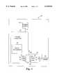
- FIG. 1is a block diagram of a computer system including an I/O printed circuit board (PCB) having a ferrite attenuator according to the present invention.
- PCBprinted circuit board
- FIG. 2is a block diagram of a computer system including a PCI back plane PCB having a ferrite attenuator according to the present invention.
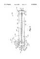
- FIG. 3is a side-view of a PCB assembly having a ferrite attenuator assembly according to the present invention attached thereto.
- FIG. 4is a perspective view of the PCB assembly of FIG. 3 with an exploded view of the ferrite attenuator assembly according to the present invention.
- Computer system 20includes a system core printed circuit board (PCB) 22 having a microprocessor 24 for performing sequences of logical operations.
- An input/output (I/O) PCB 26is coupled to system core PCB 22 via a connector 28 on I/O PCB 26 and a corresponding connector 30 on system core PCB 22.
- a power supply 32supplies power to system core PCB 22 via power rails 34.
- System core PCB 22which includes microprocessor 24 constitutes a distinct domain which includes energetic EMI noise sources. Therefore, the system core PCB 22 domain is partitioned from the rest of computer system 20 to block and isolate most of the direct radiated EMI noise signals from entering other susceptible domains.
- I/O PCB 26constitutes one such susceptible domain, which itself is not a significant contributor to the total direct radiated EMI noise produced by computer system 20. I/O PCB 26 is, however, susceptible to conducting common mode energy EMI noise signals if these EMI noise signals are not properly contained.
- System core PCB 22provides I/O signals to connector 30 on I/O signal paths 36.
- System core PCB 22provides power to connector 30 through power paths 38.
- System core PCBprovides a ground level to connector 30 through ground paths 40.
- the I/O signals conducted on I/O signal paths 36, the power conducted on power paths 38, and the ground level coupled on ground paths 40are all conducted through connector 30 to connector 28 of I/O PCB 26.
- I/O PCB 26includes I/O signal paths 42 for carrying I/O signals between connector 28 and I/O PCB 26. /O PCB 26 includes power paths 44 for conducting power to I/O PCB 26 from connector 28. I/O PCB 26 includes ground paths 46 for connecting I/O PCB 26 to a ground level.
- a ferrite attenuator or suppressor 50is installed around I/O PCB 26 at a location as close as possible to connector 28. Ferrite attenuator 50 surrounds I/O signal paths 42, power paths 44, and ground paths 46 so that all signals including power and ground are surrounded by the ferrite material of ferrite attenuator 50 to suppress common mode energy EMI noise signals. Ferrite attenuator 50 is positioned and locked in place relative to I/O PCB 26.
- I/O PCBincludes cable connectors 52 for coupling cables 54 to I/O PCB 26.
- Cables 54carry external signals to and from I/O PCB 26.
- Cables 54provide a low-resistance source for conducting common mode energy EMI noise signals to free space, but ferrite attenuator 50 suppresses the common mode energy EMI noise signals close to their source (i.e., system core PCB 22), before the EMI signals reach cables 54.
- ferrite attenuator 50elevates EMI noise source impedance via electrical losses in ferrite attenuator 50 to suppress the common mode energy EMI noise signals. As a result, common mode energy EMI noise propagation to free space is significantly reduced. Ferrite attenuator 50 more effectively suppresses common mode energy EMI, because ferrite attenuator 50 suppresses common mode energy EMI close to its source (i.e., system core PCB 22).
- ferrite attenuator 50isolates and suppresses conducted common mode energy EMI noise signals at a point where these EMI noise signals first enter the I/O PCB 26 susceptible domain.
- Computer system 120includes a system core PCB 122 having a microprocessor 124 for performing sequences of logical operations.
- a peripheral component interconnect (PCI) back plane PCB 126is coupled to system core PCB 122 via a connector 128 on PCI back plane PCB 126 and a corresponding connector 130 on system core PCB 122.
- a power supply 132supplies power to system core PCB 122 via power rails 134.
- Computer system 120also includes a PCI card 136 which is insertable into a PCI slot 138 of PCI back plane PCB 126.
- PCI card 136includes cable connectors 140 for coupling cables 142 to PCI card 136. Cables 142 carry external signals to and from PCI card 136.
- System core PCB 122which includes microprocessor 124 constitutes a distinct domain which includes energetic EMI noise sources. Therefore, the system core PCB 122 domain is partitioned from the rest of computer system 120 to block and isolate most of the direct radiated EMI noise signals from entering other susceptible domains.
- PCI back plane PCB 126 and PCI card 136constitute two such susceptible domains which themselves are not significant contributors to the total direct radiated EMI noise produced by computer system 120.
- PCI back plane PCB 126 and PCI card 136are, however, susceptible to conducting common mode energy EMI noise signals if these EMI noise signals are not properly contained.
- System core PCB 122provides I/O signals to connector 130 on I/O signal paths 144.
- System core PCB 122provides power to connector 130 through power paths 146.
- System core PCBprovides a ground level to connector 130 through ground paths 148 The I/O signals conducted on I/O signal paths 144, the power conducted on power paths 146, and the ground level coupled on ground paths 148 are all conducted through connector 130 to connector 128 of PCI back plane PCB 126.
- PCI back plane PCB 126includes I/O signal paths 152 for carrying I/O signals between connector 128 and PCI back plane PCB 126.
- PCI back plane PCB 126includes power paths 154 for conducting power to PCI back plane PCB 126 from connector 128.
- PCI back plane PCB 126includes ground paths 156 for connecting PCI back plane PCB 126 to a ground level.
- PCI card 136includes I/O signal paths 158 for carrying I/O signals between PCI slot 138 and PCI card 136.
- PCI card 136includes power paths 160 for conducting power to PCI card 136 from PCI slot 138.
- PCI card 136includes ground paths 162 for connecting PCI card 136 to a ground level.
- a ferrite attenuator 150is installed around PCI back plane PCB 126 at a location as close as possible to connector 128. Ferrite attenuator 150 surrounds I/O signal paths 152, power paths 154, and ground paths 156 so that all signals including power and ground are surrounded by the ferrite material of ferrite attenuator 150 to suppress common mode energy EMI noise signals. Ferrite attenuator 150 is positioned and locked in place relative to PCI back plane PCB 126.
- Cables 142 attached to PCI card 136provide a low-resistance source for conducting common mode energy EMI noise signals to free space, but ferrite attenuator 150 installed on PCI back plane PCB 126 suppresses the common mode energy EMI noise signals close to their source (i.e., system core PCB 122) before the EMI noise signals read cables 142.
- ferrite attenuator 150elevates EMI noise source impedance via electrical losses in ferrite attenuator 150 to suppress the common mode energy EMI noise signals. As a result, common mode energy EMI noise propagation to free space is significantly reduced. Ferrite attenuator 150 more effectively suppresses common mode energy EMI because ferrite attenuator 150 suppresses common mode energy EMI close to its source (i.e., system core PCB 22).
- ferrite attenuator 150isolates and suppresses conducted common mode energy EMI noise signals at a point where these EMI noise signals first enter the I/O PCB 26 susceptible domain.
- FIGS. 3 and 4both illustrate a PCB assembly 200 having one embodiment of a ferrite attenuator assembly 202 according to the present invention.
- FIG. 3is a side-view of PCB assembly 200
- FIG. 4is a perspective view of PCB assembly 200 where ferrite attenuator assembly 202 is illustrated in an exploded view.
- PCB assembly 200includes a PCB 204.
- Ferrite attenuator assembly 202includes an upper ferrite attenuator portion 206 and a lower ferrite attenuator portion 208.
- Ferrite attenuator portions 206 and 208are each "C" shaped and fit together around a portion of PCB 204 having I/O signal paths, power paths, and ground paths.
- PCB 204includes a first cut-out portion 210 and a second cut-out portion 212 formed therein. Cut-out portions 210 and 212 provide openings for disposing ends 214 and 216 of upper ferrite attenuator 25 portion 206 and ends 218 and 220 of lower ferrite attenuator portion 208. End 214 of upper ferrite attenuator portion 206 mates with end 218 of lower ferrite attenuator portion 208 in cut-out portion 210 of PCB 204. End 216 of upper ferrite attenuator portion 206 mates with end 220 of lower ferrite attenuator portion 208 in cut-out portion 212 of PCB 204.
- Cshaped ferrite attenuator portions 206 and 208 together form a ferrite attenuator ring around a signal carrying portion 222 of PCB 204 which includes all I/O signal paths, power paths, and ground paths to and from PCB 204. In this way, all signals including power and ground are surrounded by the ferrite attenuator ring formed by ferrite attenuator portions 206 and 208 to suppress common mode energy EMI noise signals carried on the signal paths.
- Ferrite attenuator assembly 202includes an upper foam pad dampener 228 disposed between upper ferrite attenuator portion 206 and the top side of signal carrying PCB portion 222. Ferrite attenuator assembly 202 also includes a lower foam pad dampener 230 disposed between lower ferrite attenuator portion 208 and the bottom side of signal carrying PCB portion 222 of PCB 204.
- Upper foam pad dampener 228fills upper gap 224 and lower foam pad dampener 230 fills lower gap 226.
- Upper foam pad dampener 228is preferably attached to the inside face of upper ferrite attenuator portion 206 and lower foam pad dampener 230 is preferably attached to the inside face of lower ferrite attenuator portion 208.
- Foam pad dampeners 228 and 230dampen shock exerted on ferrite attenuator portions 206 and 208, which can occur during system handling and system use to protect the ferrite material which forms ferrite attenuator portions 206 and 208 from breaking, as ferrite material is very brittle.
- foam pad dampeners 228 and 230fill up gaps 224 and 226 respectively, to accommodate various thicknesses of PCBs 204.
- various tolerance stacks from differing height and sized integrated circuit chips and other components attached to PCB 204 at signal carrying portion 222are accommodated by using foam pad dampeners 228 and 230.
- the sensitive integrated circuit chips and other components attached to PCB 204 at signal carrying portion 222are also protected from shock exerted during system handling and system use.
- Ferrite attenuator assembly 202also includes clips 232 and 234, which are metal clips in one embodiment of the present invention.
- Metal clip 232fits over end 214 of upper ferrite attenuator portion 206 and end 218 of lower ferrite attenuator portion 208 to secure the mated ends together.
- metal clip 234fits over end 216 of upper ferrite attenuator portion 206 and end 220 of lower ferrite attenuator portion 208 to secure the mated ends together.
- Metal clips 232 and 234provide force to compress foam pad dampeners 228 and 230 between PCB 204 and the ferrite attenuator portions 206 and 208 to obtain elastic attachment of the ferrite attenuator portions to PCB 204.
- Metal clip 232includes an upper jaw 236, a lower jaw 238, and a back wall 242.
- Lower jaw 238includes a flat portion 240 extending inwardly from back wall 242.
- Lower jaw 238includes a lead-in portion 244 extending inwardly from flat portion 240 at the end of the lower jaw.
- Lead-in portion 244extends downwardly at an angle, indicated by arrows 246, which in one example embodiment is approximately 10 degrees.
- Upper jaw 236includes an angled jaw portion 248 which extends inwardly and downwardly from back-wall 242 at an angle, indicated by arrows 250, which in one example embodiment is approximately 40 degrees.
- Upper jaw 236includes a lead-in portion 252 extending inwardly at an upward angle from angled jaw portion 248, as indicated by arrows 254, which indicate an angle formed by lead-in portion 252 and a line perpendicular to PCB 204. In one example embodiment, angle 254 is approximately 35 degrees.
- An elbow 256is formed in upper jaw 236 at the junction between angled jaw portion 248 and lead-in portion 252.
- Lead-in portion 252has a lead-in angel from elbow 256, indicated by arrows 260. In the example embodiment where the angle indicated by arrows 254 is approximately 35 degrees, lead-in angle 260 is approximately 55 degrees.
- each of the ends 214, 216, 218, and 220 of ferrite attenuator portions 206 and 208include the following features, which are described with respect to ends 214 and 218.
- a ramp 262is located on end 214 of ferrite attenuator portion 206 and has an angle indicated by arrows 264, which in an example embodiment is approximately 45 degrees.
- a substantially similar ramp 266is located on end 218 of ferrite attenuator portion 208.
- a flat portion 268extends inwardly from ramp 262, and a flat portion 270 extends inwardly from ramp 266.
- a grove 272is located inward from flat portion 268 and a grove 274 is located inward from flat portion 270.
- the angles of elbow 256match the angles of groove 272, such that a first wall of groove 272 extends inwardly and downwardly from flat portion 268 at an angle indicated by arrows 250 (e.g. 40 degrees in one example embodiment), and a second wall of groove 272 extends inwardly and upwardly from the first wall of groove 272 at an angle indicated by arrows 254 (e.g., 35 degrees in an example embodiment), which indicate an angle formed by the second wall of groove 272 and a line perpendicular to PCB 204.
- Metal clip 232easily slides over ferrite attenuator portions 206 and 208, because lead-in portion 252 of the upper jaw of clip 232 slides over ramp 262 of ferrite attenuator portion 206, and lead-in portion 244 of the lower jaw of clip 232 slides over ramp 266 of ferrite attenuator portion 208. Furthermore, elbow 256 of the upper jaw of clip 232 snaps securely into groove 272 of ferrite attenuator portion 206. In addition, flat portion 240 of the lower jaw of clip 232 matches flat portion 270 of ferrite attenuator portion 208.
- Metal clips 232 and 234include lead-in portions on their upper and lower jaws to permit easy sliding of the clips over ferrite attenuator portions 206 and 208, so that the ferrite attenuator portions are clamped together without damaging the ferrite material that forms the ferrite attenuator portions, as ferrite material is quite fragile and brittle.
- a systemsuch as computer systems 20 and 120 which incorporate a PCB assembly, such as PCB assembly 200 according to the present invention, suppresses common mode energy EMI noise which propagates through interconnecting electrical paths, power paths, and ground paths between domains as close as possible to the source of the EMI noise by surrounding the input/output signal paths, the power paths, and the ground paths with a ferrite attenuator, such as formed by ferrite attenuator portions 206 and 208.
- the cost of such a system according to the present inventionis low compared to the conventional technique of installing ferrite around each individual cable.
- one ferrite attenuatorsurrounds all of the signal paths between an EMI generating domain and an adjacent EMI conducting domain.
- EMI noiseis suppressed at the domain adjacent the EMI generating domain.
- a larger percentage of common mode energy EMI noiseis suppressed with the ferrite attenuator being as close as possible to the source of the EMI noise, because the effective increase in EMI noise source impedance becomes greater as the ferrite attenuator is disposed closer to the EMI source.
Landscapes
- Engineering & Computer Science (AREA)
- Microelectronics & Electronic Packaging (AREA)
- Physics & Mathematics (AREA)
- Electromagnetism (AREA)
- Shielding Devices Or Components To Electric Or Magnetic Fields (AREA)
Abstract
Description
Claims (20)
Priority Applications (2)
| Application Number | Priority Date | Filing Date | Title |
|---|---|---|---|
| US09/274,722US6125044A (en) | 1999-03-23 | 1999-03-23 | Suppressing EMI with PCB mounted ferrite attenuator |
| JP2000064539AJP2000277971A (en) | 1999-03-23 | 2000-03-09 | Method and device for suppressing emi |
Applications Claiming Priority (1)
| Application Number | Priority Date | Filing Date | Title |
|---|---|---|---|
| US09/274,722US6125044A (en) | 1999-03-23 | 1999-03-23 | Suppressing EMI with PCB mounted ferrite attenuator |
Publications (1)
| Publication Number | Publication Date |
|---|---|
| US6125044Atrue US6125044A (en) | 2000-09-26 |
Family
ID=23049353
Family Applications (1)
| Application Number | Title | Priority Date | Filing Date |
|---|---|---|---|
| US09/274,722Expired - LifetimeUS6125044A (en) | 1999-03-23 | 1999-03-23 | Suppressing EMI with PCB mounted ferrite attenuator |
Country Status (2)
| Country | Link |
|---|---|
| US (1) | US6125044A (en) |
| JP (1) | JP2000277971A (en) |
Cited By (53)
| Publication number | Priority date | Publication date | Assignee | Title |
|---|---|---|---|---|
| WO2002021639A1 (en)* | 2000-09-08 | 2002-03-14 | Viewtech Ic Co., Ltd. | D-subconnector provided with ferrite cores |
| US20030057966A1 (en)* | 2001-07-13 | 2003-03-27 | Kenji Shimazaki | Electromagnetic interference analysis method and apparatus |
| US6603080B2 (en)* | 2001-09-27 | 2003-08-05 | Andrew Corporation | Circuit board having ferrite powder containing layer |
| US6687135B1 (en)* | 1999-11-19 | 2004-02-03 | Murata Manufacturing Co., Ltd. | Electronic component with shield case |
| US20040197284A1 (en)* | 2003-04-04 | 2004-10-07 | Frederic Auguste | Cosmetic composition comprising a volatile fatty phase |
| US20050013125A1 (en)* | 2003-07-14 | 2005-01-20 | Dobbs Robert William | Assembly for supporting a short printed circuit card |
| US20050013123A1 (en)* | 2003-07-14 | 2005-01-20 | Barr Andrew Harvey | Supporting a short printed circuit card |
| US6873513B2 (en) | 1997-04-08 | 2005-03-29 | X2Y Attenuators, Llc | Paired multi-layered dielectric independent passive component architecture resulting in differential and common mode filtering with surge protection in one integrated package |
| US6894884B2 (en) | 1997-04-08 | 2005-05-17 | Xzy Attenuators, Llc | Offset pathway arrangements for energy conditioning |
| US6954346B2 (en) | 1997-04-08 | 2005-10-11 | Xzy Attenuators, Llc | Filter assembly |
| US7042703B2 (en) | 2000-03-22 | 2006-05-09 | X2Y Attenuators, Llc | Energy conditioning structure |
| US7042303B2 (en) | 1998-04-07 | 2006-05-09 | X2Y Attenuators, Llc | Energy conditioning circuit assembly |
| US7050284B2 (en) | 1997-04-08 | 2006-05-23 | X2Y Attenuators, Llc | Component carrier |
| US7106570B2 (en) | 1997-04-08 | 2006-09-12 | Xzy Altenuators, Llc | Pathway arrangement |
| US7110235B2 (en) | 1997-04-08 | 2006-09-19 | Xzy Altenuators, Llc | Arrangement for energy conditioning |
| US7110227B2 (en) | 1997-04-08 | 2006-09-19 | X2Y Attenuators, Llc | Universial energy conditioning interposer with circuit architecture |
| US7113383B2 (en) | 2000-04-28 | 2006-09-26 | X2Y Attenuators, Llc | Predetermined symmetrically balanced amalgam with complementary paired portions comprising shielding electrodes and shielded electrodes and other predetermined element portions for symmetrically balanced and complementary energy portion conditioning |
| US7141899B2 (en) | 1998-04-07 | 2006-11-28 | X2Y Attenuators, Llc | Component carrier |
| US7180718B2 (en) | 2003-01-31 | 2007-02-20 | X2Y Attenuators, Llc | Shielded energy conditioner |
| US7193831B2 (en) | 2000-10-17 | 2007-03-20 | X2Y Attenuators, Llc | Energy pathway arrangement |
| US7224564B2 (en) | 2000-10-17 | 2007-05-29 | X2Y Attenuators, Llc | Amalgam of shielding and shielded energy pathways and other elements for single or multiple circuitries with common reference node |
| US7262949B2 (en) | 2000-08-15 | 2007-08-28 | X2Y Attenuators, Llc | Electrode arrangement for circuit energy conditioning |
| US7274549B2 (en) | 2000-12-15 | 2007-09-25 | X2Y Attenuators, Llc | Energy pathway arrangements for energy conditioning |
| US7301748B2 (en) | 1997-04-08 | 2007-11-27 | Anthony Anthony A | Universal energy conditioning interposer with circuit architecture |
| US7321485B2 (en) | 1997-04-08 | 2008-01-22 | X2Y Attenuators, Llc | Arrangement for energy conditioning |
| US7336468B2 (en) | 1997-04-08 | 2008-02-26 | X2Y Attenuators, Llc | Arrangement for energy conditioning |
| US7336467B2 (en) | 2000-10-17 | 2008-02-26 | X2Y Attenuators, Llc | Energy pathway arrangement |
| US7423860B2 (en) | 1997-04-08 | 2008-09-09 | X2Y Attenuators, Llc | Multi-functional energy conditioner |
| US7427816B2 (en) | 1998-04-07 | 2008-09-23 | X2Y Attenuators, Llc | Component carrier |
| US7440252B2 (en) | 2003-05-29 | 2008-10-21 | X2Y Attenuators, Llc | Connector related structures including an energy conditioner |
| US7443647B2 (en) | 1997-04-08 | 2008-10-28 | X2Y Attenuators, Llc | Paired multi-layered dielectric independent passive component architecture resulting in differential and common mode filtering with surge protection in one integrated package |
| US7586728B2 (en) | 2005-03-14 | 2009-09-08 | X2Y Attenuators, Llc | Conditioner with coplanar conductors |
| US7630188B2 (en) | 2005-03-01 | 2009-12-08 | X2Y Attenuators, Llc | Conditioner with coplanar conductors |
| US7675729B2 (en) | 2003-12-22 | 2010-03-09 | X2Y Attenuators, Llc | Internally shielded energy conditioner |
| US20100200281A1 (en)* | 2009-02-06 | 2010-08-12 | Tatung Company | Circuit board structure |
| US7817397B2 (en) | 2005-03-01 | 2010-10-19 | X2Y Attenuators, Llc | Energy conditioner with tied through electrodes |
| US20110175750A1 (en)* | 2008-03-21 | 2011-07-21 | The Trustees Of Columbia University In The City Of New York | Decision Support Control Centers |
| US20110231213A1 (en)* | 2008-03-21 | 2011-09-22 | The Trustees Of Columbia University In The City Of New York | Methods and systems of determining the effectiveness of capital improvement projects |
| US8026777B2 (en) | 2006-03-07 | 2011-09-27 | X2Y Attenuators, Llc | Energy conditioner structures |
| US20110282703A1 (en)* | 2010-05-11 | 2011-11-17 | Consolidated Edison Company Of New York, Inc. | Contingency analysis information for utility service network |
| US8560476B2 (en) | 2003-08-26 | 2013-10-15 | The Trustees Of Columbia University In The City Of New York | Martingale control of production for optimal profitability of oil and gas fields |
| US8725625B2 (en) | 2009-05-28 | 2014-05-13 | The Trustees Of Columbia University In The City Of New York | Capital asset planning system |
| US8725665B2 (en) | 2010-02-24 | 2014-05-13 | The Trustees Of Columbia University In The City Of New York | Metrics monitoring and financial validation system (M2FVS) for tracking performance of capital, operations, and maintenance investments to an infrastructure |
| US8751421B2 (en) | 2010-07-16 | 2014-06-10 | The Trustees Of Columbia University In The City Of New York | Machine learning for power grid |
| US20140182921A1 (en)* | 2012-12-28 | 2014-07-03 | Hitachi Metals, Ltd. | Wire harness |
| US9054094B2 (en) | 1997-04-08 | 2015-06-09 | X2Y Attenuators, Llc | Energy conditioning circuit arrangement for integrated circuit |
| US9204531B2 (en) | 2012-06-13 | 2015-12-01 | International Business Machines Corporation | Implementing feed-through and domain isolation using ferrite and containment barriers |
| US9395707B2 (en) | 2009-02-20 | 2016-07-19 | Calm Energy Inc. | Dynamic contingency avoidance and mitigation system |
| US20180019681A1 (en)* | 2016-07-12 | 2018-01-18 | Thomson Licensing | Galvanic isolated device and corresponding method and system |
| US10178761B2 (en) | 2016-04-28 | 2019-01-08 | Hewlett Packard Enterprise Development Lp | Defected ground structure to minimize EMI radiation |
| US10186812B1 (en) | 2017-04-28 | 2019-01-22 | Universal Lighting Technologies, Inc. | Ferrite wafer and connector assembly for EMI noise suppression on a printed circuit board |
| US10186809B1 (en) | 2017-04-28 | 2019-01-22 | Universal Lighting Technologies, Inc. | Printed circuit board connector with integrated EMI noise suppression |
| US10499489B2 (en) | 2017-07-14 | 2019-12-03 | Hewlett Packard Enterprise Development Lp | Defected ground structure with void having resistive material along perimeter to improve EMI suppression |
Families Citing this family (1)
| Publication number | Priority date | Publication date | Assignee | Title |
|---|---|---|---|---|
| JP5235031B2 (en)* | 2011-03-15 | 2013-07-10 | 島田理化工業株式会社 | Limiter device, radar system |
Citations (4)
| Publication number | Priority date | Publication date | Assignee | Title |
|---|---|---|---|---|
| US5416427A (en)* | 1993-02-11 | 1995-05-16 | Tracewell Enclosures, Inc. | Test and development apparatus for bus-based circuit modules with open side and backplane access features |
| US5570270A (en)* | 1994-06-03 | 1996-10-29 | Pulse Electronics, Inc. | Chassis and personal computer for severe environment embedded applications |
| US5604352A (en)* | 1995-04-25 | 1997-02-18 | Raychem Corporation | Apparatus comprising voltage multiplication components |
| US5652553A (en)* | 1993-03-22 | 1997-07-29 | Siemens Nixdorf Informationssysteme Aktiengesellschaft | Signal transmission between modules connected to a common backplane |
- 1999
- 1999-03-23USUS09/274,722patent/US6125044A/ennot_activeExpired - Lifetime
- 2000
- 2000-03-09JPJP2000064539Apatent/JP2000277971A/enactivePending
Patent Citations (5)
| Publication number | Priority date | Publication date | Assignee | Title |
|---|---|---|---|---|
| US5416427A (en)* | 1993-02-11 | 1995-05-16 | Tracewell Enclosures, Inc. | Test and development apparatus for bus-based circuit modules with open side and backplane access features |
| US5652553A (en)* | 1993-03-22 | 1997-07-29 | Siemens Nixdorf Informationssysteme Aktiengesellschaft | Signal transmission between modules connected to a common backplane |
| US5570270A (en)* | 1994-06-03 | 1996-10-29 | Pulse Electronics, Inc. | Chassis and personal computer for severe environment embedded applications |
| US5604352A (en)* | 1995-04-25 | 1997-02-18 | Raychem Corporation | Apparatus comprising voltage multiplication components |
| US5748464A (en)* | 1995-04-25 | 1998-05-05 | Raychem Corporation | Apparatus comprising inductive and/or power transfer and/or voltage multiplication components |
Non-Patent Citations (2)
| Title |
|---|
| "Ferrite RFI Suppressors", FerriShield, Inc., Interference Control Components Catalog (1997). |
| Ferrite RFI Suppressors , FerriShield, Inc., Interference Control Components Catalog (1997).* |
Cited By (82)
| Publication number | Priority date | Publication date | Assignee | Title |
|---|---|---|---|---|
| US7609501B2 (en) | 1997-04-08 | 2009-10-27 | X2Y Attenuators, Llc | Manufacture including shield structure |
| US7733621B2 (en) | 1997-04-08 | 2010-06-08 | X2Y Attenuators, Llc | Energy conditioning circuit arrangement for integrated circuit |
| US8004812B2 (en) | 1997-04-08 | 2011-08-23 | X2Y Attenuators, Llc | Energy conditioning circuit arrangement for integrated circuit |
| US8023241B2 (en) | 1997-04-08 | 2011-09-20 | X2Y Attenuators, Llc | Arrangement for energy conditioning |
| US7920367B2 (en) | 1997-04-08 | 2011-04-05 | X2Y Attenuators, Llc | Method for making arrangement for energy conditioning |
| US7916444B2 (en) | 1997-04-08 | 2011-03-29 | X2Y Attenuators, Llc | Arrangement for energy conditioning |
| US7321485B2 (en) | 1997-04-08 | 2008-01-22 | X2Y Attenuators, Llc | Arrangement for energy conditioning |
| US9019679B2 (en) | 1997-04-08 | 2015-04-28 | X2Y Attenuators, Llc | Arrangement for energy conditioning |
| US9036319B2 (en) | 1997-04-08 | 2015-05-19 | X2Y Attenuators, Llc | Arrangement for energy conditioning |
| US6873513B2 (en) | 1997-04-08 | 2005-03-29 | X2Y Attenuators, Llc | Paired multi-layered dielectric independent passive component architecture resulting in differential and common mode filtering with surge protection in one integrated package |
| US6894884B2 (en) | 1997-04-08 | 2005-05-17 | Xzy Attenuators, Llc | Offset pathway arrangements for energy conditioning |
| US6954346B2 (en) | 1997-04-08 | 2005-10-11 | Xzy Attenuators, Llc | Filter assembly |
| US7768763B2 (en) | 1997-04-08 | 2010-08-03 | X2Y Attenuators, Llc | Arrangement for energy conditioning |
| US7423860B2 (en) | 1997-04-08 | 2008-09-09 | X2Y Attenuators, Llc | Multi-functional energy conditioner |
| US7301748B2 (en) | 1997-04-08 | 2007-11-27 | Anthony Anthony A | Universal energy conditioning interposer with circuit architecture |
| US7050284B2 (en) | 1997-04-08 | 2006-05-23 | X2Y Attenuators, Llc | Component carrier |
| US7106570B2 (en) | 1997-04-08 | 2006-09-12 | Xzy Altenuators, Llc | Pathway arrangement |
| US7110235B2 (en) | 1997-04-08 | 2006-09-19 | Xzy Altenuators, Llc | Arrangement for energy conditioning |
| US7110227B2 (en) | 1997-04-08 | 2006-09-19 | X2Y Attenuators, Llc | Universial energy conditioning interposer with circuit architecture |
| US7688565B2 (en) | 1997-04-08 | 2010-03-30 | X2Y Attenuators, Llc | Arrangements for energy conditioning |
| US9054094B2 (en) | 1997-04-08 | 2015-06-09 | X2Y Attenuators, Llc | Energy conditioning circuit arrangement for integrated circuit |
| US7336468B2 (en) | 1997-04-08 | 2008-02-26 | X2Y Attenuators, Llc | Arrangement for energy conditioning |
| US8018706B2 (en) | 1997-04-08 | 2011-09-13 | X2Y Attenuators, Llc | Arrangement for energy conditioning |
| US7609500B2 (en) | 1997-04-08 | 2009-10-27 | X2Y Attenuators, Llc | Universal energy conditioning interposer with circuit architecture |
| US7593208B2 (en) | 1997-04-08 | 2009-09-22 | X2Y Attenuators, Llc | Multi-functional energy conditioner |
| US9373592B2 (en) | 1997-04-08 | 2016-06-21 | X2Y Attenuators, Llc | Arrangement for energy conditioning |
| US7443647B2 (en) | 1997-04-08 | 2008-10-28 | X2Y Attenuators, Llc | Paired multi-layered dielectric independent passive component architecture resulting in differential and common mode filtering with surge protection in one integrated package |
| US8587915B2 (en) | 1997-04-08 | 2013-11-19 | X2Y Attenuators, Llc | Arrangement for energy conditioning |
| US7042303B2 (en) | 1998-04-07 | 2006-05-09 | X2Y Attenuators, Llc | Energy conditioning circuit assembly |
| US7427816B2 (en) | 1998-04-07 | 2008-09-23 | X2Y Attenuators, Llc | Component carrier |
| US7141899B2 (en) | 1998-04-07 | 2006-11-28 | X2Y Attenuators, Llc | Component carrier |
| US6687135B1 (en)* | 1999-11-19 | 2004-02-03 | Murata Manufacturing Co., Ltd. | Electronic component with shield case |
| US7042703B2 (en) | 2000-03-22 | 2006-05-09 | X2Y Attenuators, Llc | Energy conditioning structure |
| US7113383B2 (en) | 2000-04-28 | 2006-09-26 | X2Y Attenuators, Llc | Predetermined symmetrically balanced amalgam with complementary paired portions comprising shielding electrodes and shielded electrodes and other predetermined element portions for symmetrically balanced and complementary energy portion conditioning |
| US7262949B2 (en) | 2000-08-15 | 2007-08-28 | X2Y Attenuators, Llc | Electrode arrangement for circuit energy conditioning |
| WO2002021639A1 (en)* | 2000-09-08 | 2002-03-14 | Viewtech Ic Co., Ltd. | D-subconnector provided with ferrite cores |
| US7336467B2 (en) | 2000-10-17 | 2008-02-26 | X2Y Attenuators, Llc | Energy pathway arrangement |
| US7224564B2 (en) | 2000-10-17 | 2007-05-29 | X2Y Attenuators, Llc | Amalgam of shielding and shielded energy pathways and other elements for single or multiple circuitries with common reference node |
| US7193831B2 (en) | 2000-10-17 | 2007-03-20 | X2Y Attenuators, Llc | Energy pathway arrangement |
| US7433168B2 (en) | 2000-10-17 | 2008-10-07 | X2Y Attenuators, Llc | Amalgam of shielding and shielded energy pathways and other elements for single or multiple circuitries with common reference node |
| US7428134B2 (en) | 2000-10-17 | 2008-09-23 | X2Y Attenuators, Llc | Energy pathway arrangements for energy conditioning |
| US7274549B2 (en) | 2000-12-15 | 2007-09-25 | X2Y Attenuators, Llc | Energy pathway arrangements for energy conditioning |
| US20030057966A1 (en)* | 2001-07-13 | 2003-03-27 | Kenji Shimazaki | Electromagnetic interference analysis method and apparatus |
| US6754598B2 (en)* | 2001-07-13 | 2004-06-22 | Matsushita Electric Industrial Co., Ltd. | Electromagnetic interference analysis method and apparatus |
| US6603080B2 (en)* | 2001-09-27 | 2003-08-05 | Andrew Corporation | Circuit board having ferrite powder containing layer |
| US7180718B2 (en) | 2003-01-31 | 2007-02-20 | X2Y Attenuators, Llc | Shielded energy conditioner |
| US20040197284A1 (en)* | 2003-04-04 | 2004-10-07 | Frederic Auguste | Cosmetic composition comprising a volatile fatty phase |
| US7440252B2 (en) | 2003-05-29 | 2008-10-21 | X2Y Attenuators, Llc | Connector related structures including an energy conditioner |
| US6967850B2 (en) | 2003-07-14 | 2005-11-22 | Hewlett-Packard Development Company, L.P. | Supporting a short printed circuit card |
| US6856518B2 (en) | 2003-07-14 | 2005-02-15 | Hewlett Packard Development Company, L.P. | Assembly for supporting a short printed circuit card |
| US20050013123A1 (en)* | 2003-07-14 | 2005-01-20 | Barr Andrew Harvey | Supporting a short printed circuit card |
| US20050013125A1 (en)* | 2003-07-14 | 2005-01-20 | Dobbs Robert William | Assembly for supporting a short printed circuit card |
| US8560476B2 (en) | 2003-08-26 | 2013-10-15 | The Trustees Of Columbia University In The City Of New York | Martingale control of production for optimal profitability of oil and gas fields |
| US7675729B2 (en) | 2003-12-22 | 2010-03-09 | X2Y Attenuators, Llc | Internally shielded energy conditioner |
| US7974062B2 (en) | 2005-03-01 | 2011-07-05 | X2Y Attenuators, Llc | Internally overlapped conditioners |
| US8014119B2 (en) | 2005-03-01 | 2011-09-06 | X2Y Attenuators, Llc | Energy conditioner with tied through electrodes |
| US7630188B2 (en) | 2005-03-01 | 2009-12-08 | X2Y Attenuators, Llc | Conditioner with coplanar conductors |
| US7782587B2 (en) | 2005-03-01 | 2010-08-24 | X2Y Attenuators, Llc | Internally overlapped conditioners |
| US9001486B2 (en) | 2005-03-01 | 2015-04-07 | X2Y Attenuators, Llc | Internally overlapped conditioners |
| US7817397B2 (en) | 2005-03-01 | 2010-10-19 | X2Y Attenuators, Llc | Energy conditioner with tied through electrodes |
| US8547677B2 (en) | 2005-03-01 | 2013-10-01 | X2Y Attenuators, Llc | Method for making internally overlapped conditioners |
| US7586728B2 (en) | 2005-03-14 | 2009-09-08 | X2Y Attenuators, Llc | Conditioner with coplanar conductors |
| US8026777B2 (en) | 2006-03-07 | 2011-09-27 | X2Y Attenuators, Llc | Energy conditioner structures |
| US8972066B2 (en) | 2008-03-21 | 2015-03-03 | The Trustees Of Columbia University In The City Of New York | Decision support control centers |
| US20110231213A1 (en)* | 2008-03-21 | 2011-09-22 | The Trustees Of Columbia University In The City Of New York | Methods and systems of determining the effectiveness of capital improvement projects |
| US20110175750A1 (en)* | 2008-03-21 | 2011-07-21 | The Trustees Of Columbia University In The City Of New York | Decision Support Control Centers |
| US20100200281A1 (en)* | 2009-02-06 | 2010-08-12 | Tatung Company | Circuit board structure |
| US8093504B2 (en) | 2009-02-06 | 2012-01-10 | Tatung Company | Circuit board structure employing ferrite element |
| US9395707B2 (en) | 2009-02-20 | 2016-07-19 | Calm Energy Inc. | Dynamic contingency avoidance and mitigation system |
| US8725625B2 (en) | 2009-05-28 | 2014-05-13 | The Trustees Of Columbia University In The City Of New York | Capital asset planning system |
| US8725665B2 (en) | 2010-02-24 | 2014-05-13 | The Trustees Of Columbia University In The City Of New York | Metrics monitoring and financial validation system (M2FVS) for tracking performance of capital, operations, and maintenance investments to an infrastructure |
| US8583405B2 (en)* | 2010-05-11 | 2013-11-12 | Maggie Chow | Contingency analysis information for utility service network |
| US20110282703A1 (en)* | 2010-05-11 | 2011-11-17 | Consolidated Edison Company Of New York, Inc. | Contingency analysis information for utility service network |
| US8751421B2 (en) | 2010-07-16 | 2014-06-10 | The Trustees Of Columbia University In The City Of New York | Machine learning for power grid |
| US9204531B2 (en) | 2012-06-13 | 2015-12-01 | International Business Machines Corporation | Implementing feed-through and domain isolation using ferrite and containment barriers |
| US20140182921A1 (en)* | 2012-12-28 | 2014-07-03 | Hitachi Metals, Ltd. | Wire harness |
| US9258933B2 (en)* | 2012-12-28 | 2016-02-09 | Hitachi Metals, Ltd. | Wire harness |
| US10178761B2 (en) | 2016-04-28 | 2019-01-08 | Hewlett Packard Enterprise Development Lp | Defected ground structure to minimize EMI radiation |
| US20180019681A1 (en)* | 2016-07-12 | 2018-01-18 | Thomson Licensing | Galvanic isolated device and corresponding method and system |
| US10186812B1 (en) | 2017-04-28 | 2019-01-22 | Universal Lighting Technologies, Inc. | Ferrite wafer and connector assembly for EMI noise suppression on a printed circuit board |
| US10186809B1 (en) | 2017-04-28 | 2019-01-22 | Universal Lighting Technologies, Inc. | Printed circuit board connector with integrated EMI noise suppression |
| US10499489B2 (en) | 2017-07-14 | 2019-12-03 | Hewlett Packard Enterprise Development Lp | Defected ground structure with void having resistive material along perimeter to improve EMI suppression |
Also Published As
| Publication number | Publication date |
|---|---|
| JP2000277971A (en) | 2000-10-06 |
Similar Documents
| Publication | Publication Date | Title |
|---|---|---|
| US6125044A (en) | Suppressing EMI with PCB mounted ferrite attenuator | |
| US6205026B1 (en) | Heat sink retention components and system | |
| JP2000347767A (en) | Computer system housing | |
| US5838542A (en) | Processor card assembly including a heat sink attachment plate and an EMI/ESD shielding cage | |
| US6166908A (en) | Integrated circuit cartridge | |
| US7612299B2 (en) | Shield assembly with gaskets | |
| JP2530051B2 (en) | Semiconductor integrated circuit device | |
| US6431718B1 (en) | Interconnector and light pipe guide for disk drive and disk drive carrier | |
| JP2001160663A (en) | Circuit substrate | |
| US7210946B2 (en) | Electronic device with EMI shield | |
| EP0834964A1 (en) | Shielded electrical receptacle connector assembly | |
| US7760515B2 (en) | Electronic device with EMI shielding assembly | |
| CN104602502B (en) | Cable back board system with electromagnetic radiation absorber | |
| US6900983B2 (en) | Removable cartridge for PCMCIA card and ancillary storage drive | |
| US20030049948A1 (en) | Apparatus and method for coupling buses | |
| US6268999B1 (en) | Computer peripheral device with integral ground clip | |
| US6627812B2 (en) | Apparatus for containing electro-magnetic interference | |
| KR200145503Y1 (en) | Grounding System for IC Cards | |
| US7529092B2 (en) | Electromagnetic interference shield and heat sink apparatus | |
| CN112423573B (en) | Electromagnetic protection device | |
| JP2004349135A (en) | connector | |
| US7173804B2 (en) | Array capacitor with IC contacts and applications | |
| EP1324089A2 (en) | Optical module | |
| US6687127B2 (en) | EMC core supporting structure | |
| US7187555B2 (en) | Card guide for expansion circuit card |
Legal Events
| Date | Code | Title | Description |
|---|---|---|---|
| AS | Assignment | Owner name:HEWLETT-PACKARD COMPANY, CALIFORNIA Free format text:ASSIGNMENT OF ASSIGNORS INTEREST;ASSIGNORS:CHERNISKI, ANDREW M.;SANDOVAL, ALISA C.;REEL/FRAME:010046/0781 Effective date:19990322 | |
| STCF | Information on status: patent grant | Free format text:PATENTED CASE | |
| FEPP | Fee payment procedure | Free format text:PAYOR NUMBER ASSIGNED (ORIGINAL EVENT CODE: ASPN); ENTITY STATUS OF PATENT OWNER: LARGE ENTITY | |
| FPAY | Fee payment | Year of fee payment:4 | |
| FPAY | Fee payment | Year of fee payment:8 | |
| REMI | Maintenance fee reminder mailed | ||
| AS | Assignment | Owner name:HEWLETT-PACKARD DEVELOPMENT COMPANY, L.P., TEXAS Free format text:ASSIGNMENT OF ASSIGNORS INTEREST;ASSIGNOR:HEWLETT-PACKARD COMPANY;REEL/FRAME:026945/0699 Effective date:20030131 | |
| FPAY | Fee payment | Year of fee payment:12 | |
| AS | Assignment | Owner name:HEWLETT PACKARD ENTERPRISE DEVELOPMENT LP, TEXAS Free format text:ASSIGNMENT OF ASSIGNORS INTEREST;ASSIGNOR:HEWLETT-PACKARD DEVELOPMENT COMPANY, L.P.;REEL/FRAME:037079/0001 Effective date:20151027 |