US6124729A - Field programmable logic arrays with vertical transistors - Google Patents
Field programmable logic arrays with vertical transistorsDownload PDFInfo
- Publication number
- US6124729A US6124729AUS09/032,617US3261798AUS6124729AUS 6124729 AUS6124729 AUS 6124729AUS 3261798 AUS3261798 AUS 3261798AUS 6124729 AUS6124729 AUS 6124729A
- Authority
- US
- United States
- Prior art keywords
- array
- programmable logic
- logic
- term
- lines
- Prior art date
- Legal status (The legal status is an assumption and is not a legal conclusion. Google has not performed a legal analysis and makes no representation as to the accuracy of the status listed.)
- Expired - Lifetime
Links
Images


Classifications
- H—ELECTRICITY
- H10—SEMICONDUCTOR DEVICES; ELECTRIC SOLID-STATE DEVICES NOT OTHERWISE PROVIDED FOR
- H10D—INORGANIC ELECTRIC SEMICONDUCTOR DEVICES
- H10D84/00—Integrated devices formed in or on semiconductor substrates that comprise only semiconducting layers, e.g. on Si wafers or on GaAs-on-Si wafers
- H10D84/90—Masterslice integrated circuits
- H10D84/903—Masterslice integrated circuits comprising field effect technology
- H—ELECTRICITY
- H03—ELECTRONIC CIRCUITRY
- H03K—PULSE TECHNIQUE
- H03K19/00—Logic circuits, i.e. having at least two inputs acting on one output; Inverting circuits
- H03K19/02—Logic circuits, i.e. having at least two inputs acting on one output; Inverting circuits using specified components
- H03K19/173—Logic circuits, i.e. having at least two inputs acting on one output; Inverting circuits using specified components using elementary logic circuits as components
- H03K19/177—Logic circuits, i.e. having at least two inputs acting on one output; Inverting circuits using specified components using elementary logic circuits as components arranged in matrix form
- H03K19/17704—Logic circuits, i.e. having at least two inputs acting on one output; Inverting circuits using specified components using elementary logic circuits as components arranged in matrix form the logic functions being realised by the interconnection of rows and columns
- H03K19/17708—Logic circuits, i.e. having at least two inputs acting on one output; Inverting circuits using specified components using elementary logic circuits as components arranged in matrix form the logic functions being realised by the interconnection of rows and columns using an AND matrix followed by an OR matrix, i.e. programmable logic arrays
- H—ELECTRICITY
- H03—ELECTRONIC CIRCUITRY
- H03K—PULSE TECHNIQUE
- H03K19/00—Logic circuits, i.e. having at least two inputs acting on one output; Inverting circuits
- H03K19/02—Logic circuits, i.e. having at least two inputs acting on one output; Inverting circuits using specified components
- H03K19/173—Logic circuits, i.e. having at least two inputs acting on one output; Inverting circuits using specified components using elementary logic circuits as components
- H03K19/177—Logic circuits, i.e. having at least two inputs acting on one output; Inverting circuits using specified components using elementary logic circuits as components arranged in matrix form
- H03K19/1778—Structural details for adapting physical parameters
- H03K19/17796—Structural details for adapting physical parameters for physical disposition of blocks
- H—ELECTRICITY
- H10—SEMICONDUCTOR DEVICES; ELECTRIC SOLID-STATE DEVICES NOT OTHERWISE PROVIDED FOR
- H10B—ELECTRONIC MEMORY DEVICES
- H10B41/00—Electrically erasable-and-programmable ROM [EEPROM] devices comprising floating gates
- H10B41/20—Electrically erasable-and-programmable ROM [EEPROM] devices comprising floating gates characterised by three-dimensional arrangements, e.g. with cells on different height levels
- H10B41/23—Electrically erasable-and-programmable ROM [EEPROM] devices comprising floating gates characterised by three-dimensional arrangements, e.g. with cells on different height levels with source and drain on different levels, e.g. with sloping channels
- H10B41/27—Electrically erasable-and-programmable ROM [EEPROM] devices comprising floating gates characterised by three-dimensional arrangements, e.g. with cells on different height levels with source and drain on different levels, e.g. with sloping channels the channels comprising vertical portions, e.g. U-shaped channels
- H—ELECTRICITY
- H10—SEMICONDUCTOR DEVICES; ELECTRIC SOLID-STATE DEVICES NOT OTHERWISE PROVIDED FOR
- H10B—ELECTRONIC MEMORY DEVICES
- H10B69/00—Erasable-and-programmable ROM [EPROM] devices not provided for in groups H10B41/00 - H10B63/00, e.g. ultraviolet erasable-and-programmable ROM [UVEPROM] devices
Definitions
- This inventionrelates generally to integrated circuits and in particular to a field programmable logic array with vertical transistors.
- VLSIvery large scale integration
- TTL integrated circuitsare versatile because they integrate only a relatively small number of commonly used logic functions.
- the drawbackis that large numbers of TTL integrated circuits are typically required for a specific application. This increases the consumption of power and board space, and drives up the overall cost of the digital system.
- Custom logic circuitsare precisely tailored to the needs of a specific application. This allows the implementation of specific circuit architectures that dramatically reduces the number of parts required for a system. However, custom logic devices require significantly greater engineering time and effort, which increases the cost to develop these circuits and may also delay the production of the end system.
- Semi-custom gate arraysare less expensive to develop and offer faster turnaround because the circuits are typically identical except for a few final-stage steps, which are customized according to the system design specifically.
- semi-custom gate arraysare less dense, so that it takes more gate array circuits than custom circuits to implement a given amount of random logic.
- PLAsprogrammable logic arrays
- FPLAsfield programmable logic arrays
- FPLAsprovide a more flexible architecture via user-programmed on-chip fuses or switches to perform specific functions for a given application.
- FPLAscan be purchased "off the shelf” like standard logic gates and are custom tailored like gate arrays in a matter of minutes.
- FPLAsTo use FPLAs, system designers draft equations describing how the hardware is to perform, and enter the equations into a FPLA programming machine. The unprogrammed FPLAs are inserted into the machine, which interprets the equations and provides appropriate signals to the device to program the FPLA which will perform the desired logic function in the user's system.
- FPLAsbased on erasable-programmable-read-only memory cells (EPROMs) fabricated with CMOS (complimentary-metal-oxide-semiconductor) technology have been introduced.
- EPROMserasable-programmable-read-only memory cells
- CMOScomplementary-metal-oxide-semiconductor
- Such devicesemploy floating gate transistors as the FPLA switches, which are programmed by hot electron effects.
- the EPROM cellsare erased by exposure to ultraviolet light or other means.
- EEPROMsElectrically Erasable Programmable Read Only Memory
- Fowler-Nordheim tunnelingcan be erased and programmed while in circuit using Fowler-Nordheim tunneling.
- EEPROMsElectrically Erasable Programmable Read Only Memory
- a disadvantage of current EEPROMsis that they have a large cell size and require two transistors per cell. Herein is where the problem lies.
- FPLAsIncreasing the storage capacity of FPLAs requires a reduction in the size of the transistors and other components in order to increase the logic array's density.
- densityis typically limited by a minimum lithographic feature size (F) imposed by lithographic processes used during fabrication.
- Flithographic feature size
- the present generation of high density FPLAsrequire an area of 8F 2 per bit of data. Therefore, there is a need in the art to provide even higher density FPLAs to support the increased density of digital systems utilizing logic functions via semiconductor integrated circuits.
- a field programmable logic array with vertical transistorsis implemented for performing desired logic functions in a user's system.
- the field programmable logic arrayis programmed out in the field and is easily reprogrammed.
- a programmable logic arraycomprises an input having a plurality of input lines for receiving an input signal, an output having a plurality of output lines, one or more arrays having an AND plane and an OR plane connected between the input and the output, wherein the AND plane and the OR plane comprise a plurality of logic cells arranged in rows and columns for providing a sum-of-products term on the output lines responsive to the received input signal.
- Each logic cellincludes at least a pair of transistors formed on opposing sides of a common pillar of semiconductor material that extends outwardly from a working surface of a substrate to form source/drain and body regions for the transistors.
- floating gateswherein each gate is associated with a side of the pillar.
- control lineswherein each control line is associated with a floating gate.
- a programmable logic arraycomprises an input having a plurality of input lines for receiving an input signal, a first array coupled to the input lines, the first array having a plurality of logic cells arranged in rows and columns for providing a product term responsive to the received input signal, and a second array having a plurality of logic cells arranged in rows and columns for receiving the product term and providing a sum term responsive to the product term, and an output having a plurality of output lines for receiving the sum term.
- Each logic cellincludes at least a pair of transistors formed on opposing sides of a common pillar of semiconductor material that extends outwardly from a working surface of a substrate to form source/drain and body regions for the transistors.
- floating gateswherein each gate is associated with a side of the pillar.
- control lineswherein each control line is associated with a floating gate.
- a programmable logic arraycomprises an array of logic cells, each logic cell including at least a pair of transistors formed on opposing sides of a common pillar of semiconductor material that forms source/drain and body regions for the transistors and at least a pair of floating gates disposed adjacent to the opposing sides of the pillar. At least one first source/drain interconnection line is formed, interconnecting one of the first source/drain regions of one of the logic cells.
- a plurality of output lines, each output line interconnecting one of the second source/drain regions of ones of the logic cells and a plurality of input lines for receiving an input signalare also formed, wherein the array of logic cells connected between the plurality of input lines and the plurality of output lines provides a logical combination responsive to the received input signal.
- a computer systemcomprises a programmable logic array having a plurality of input lines for receiving an input signal with a first array coupled to the input lines.
- the first arrayhas a plurality of logic cells arranged in rows and columns for providing a product term responsive to the received input signal.
- a second arrayhas a plurality of logic cells arranged in rows and columns for receiving the product term and providing a sum term responsive to the product term and an output having a plurality of output lines for receiving the sum term.
- Each logic cellincludes at least a pair of transistors formed on opposing sides of a common pillar of semiconductor material that extends outwardly from a working surface of a substrate to form source/drain and body regions for the transistors, and a number of floating gates wherein each gate is associated with a side of the pillar, and a number of control lines wherein each control line is associated with a floating gate.
- a method of forming a programmable logic arrayincludes several steps as described below.
- a plurality of first conductivity type semiconductor pillarsare formed upon a substrate, each pillar having top and side surfaces.
- a plurality of first source/drain regionsare formed, of a second conductivity type, each of the first source/drain regions formed proximally to an interface between the pillar and the substrate.
- a plurality of floating gatesis formed, each of the floating gates formed substantially adjacent to a portion of the side surface of one of the pillars and separated therefrom by the gate dielectric.
- a plurality of control linesare formed, each of the control lines formed substantially adjacent to one of the floating gates and insulated therefrom, such that there are two control lines between the common pillars.
- An intergate dielectricis formed, which is interposed between one of the floating gates and one of the control lines.
- An intergate dielectricis formed, which is interposed between the two control lines located between the common pillars.
- a plurality of interconnecting linesis formed for interconnecting the control lines. At least one first source/drain interconnection line interconnecting one of the first source/drain regions is formed and a plurality of data lines are formed, each data line interconnecting one of the second/source drain regions.
- a method of forming a programmable logic array on a substratecomprises the steps of forming a first source/drain layer at a surface of the substrate. Then a semiconductor epitaxial layer on the first source/drain layer is formed. Next, a second source/drain layer at a surface of the epitaxial layer is formed. Etching is performed, in a first direction, for a plurality of substantially parallel first troughs in the epitaxial layer.
- the stepscontinue with forming an insulator in the first troughs, etching, in a second direction that is substantially orthogonal to the first direction, a plurality of substantially parallel second troughs in the epitaxial layer, forming a gate dielectric layer substantially adjacent to sidewall regions of the second troughs, and forming a conductive layer in the second troughs.
- a portion of the conductive layeris removed in the second troughs such that floating gate regions are formed along the sidewall regions therein and separated from the sidewall regions by the gate dielectric layer.
- the stepsinclude forming an intergate dielectric layer on exposed portions of the floating gate regions in the second troughs, and forming control line regions between opposing floating gate regions in the second troughs and separated from the floating gate regions in the second troughs by the intergate dielectric layer.
- a method of forming a programmable logic array on a substratecomprising the steps of forming a first source/drain layer at a surface of the substrate, forming a semiconductor epitaxial layer on the first source/drain layer, forming a second source/drain layer at a surface of the epitaxial layer, etching, in a first direction, a plurality of substantially parallel first troughs in the epitaxial layer.
- the stepsalso include forming an insulator in the first troughs, etching, in a second direction that is substantially orthogonal to the first direction, a plurality of substantially parallel second troughs in the epitaxial layer, forming a gate dielectric layer substantially adjacent to sidewall regions of the second troughs, forming a conductive layer in the second troughs and removing a portion of the conductive layer in the second troughs such that floating gate regions are formed along the sidewall regions therein and separated from the sidewall regions by the gate dielectric layer.
- an intergate dielectric layeron exposed portions of the floating gate regions in the second troughs, forming split control line regions between opposing floating gate regions in the second troughs, separating from the floating gate regions in the second troughs by the intergate dielectric layer, and separating the split control lines by the intergate dielectric layer.
- bulk semiconductor and semiconductor-on-insulator embodiments of the present inventionprovide a high density field programmable logic array.
- Therearc separate floating gates on opposite sides of a pillar constituting the transistor.
- Embodiments of the inventioninclude a single control line located between floating gates or a split control line located between floating gates. If a floating gate of transistor data is used to represent a logic function, an area of only 2F 2 is needed, where F is the minimum lithographic feature size.
- the programmability of the field programmable logic arrayis particularly advantageous for selecting desired logic functions in a digital system such as a computer without having to program a logic array with a mask. If a logic change needs to be made to the field programmable logic array, selected transistors in the logic array are simply reprogrammed. There is a need in the art to provide even higher density field programmable logic arrays to further support increased densities of digital systems utilizing logic functions via semiconductor integrated circuits.
- a field programmable logic array implementing vertical transistors with either single or split control linessupports increased densities of digital systems.
- the logic function of the field programmable logic arrayis defined without having to actually mask the logic array.
- bulk semiconductor, semiconductor-on-insulator, single control lines, split control lines and floating gates of varying scopeare described. Still other and further embodiments, aspects and advantages of the invention will become apparent by reference to the drawings and by reading the following detailed description.
- FIG. 1is a simplified block diagram of a high-level organization of a digital computer.
- FIG. 2is a simplified block diagram of a field programmable logic array.
- FIG. 3is a schematic diagram illustrating generally an architecture of one embodiment of a field programmable logic array.
- FIG. 4Aillustrates a top view of a portion of an array of logic cells having a split control line.
- FIG. 4Billustrates a front view of a portion of an array of logic cells having a split control line.
- FIG. 5Aillustrates a top view of an alternative embodiment of the array of logic cells of FIG. 4A having a single control line.
- FIG. 5Billustrates a front view of an alternative embodiment of the array of logic cells of FIG. 4A having a single control line.
- FIG. 6Ais a perspective view illustrating generally one embodiment of a completed field programmable logic array, including portions of four transistors having split control lines.
- FIG. 6Bis a cross-sectional view of the completed field programmable logic array of FIG. 6A looking perpendicular to output lines OL 1 -OL n .
- FIG. 7is a plan view looking toward the working surface of a substrate, illustrating generally by way of example one embodiment of a logic cell.
- FIG. 8illustrates a side view of a substrate material having a plurality of source/drain layers on top of the substrate material for forming a field programmable logic array.
- FIG. 9illustrates a plurality of parallel first troughs extending through a plurality of layers formed on top of a substrate material.
- FIG. 10is a perspective view of a plurality of parallel second troughs orthogonal to the first troughs illustrated in FIG. 9.
- FIG. 11is a cross-sectional view looking in the direction of the second troughs illustrated in FIG. 10.
- FIG. 12is a cross-sectional view looking in the direction of the second troughs provided in FIG. 11 illustrating a barrier layer stripped from the sidewalls of the second troughs.
- FIG. 13is a cross-sectional view looking in the direction of the second troughs provided in FIG. 12 illustrating a conductive layer in the second troughs.
- FIG. 14is a perspective view of the second troughs provided in FIG. 13 illustrating spacers positioned to be used as a mask.
- FIG. 15is a perspective view illustrating a single control line formed between opposing floating gates in the second troughs provided in FIG. 14.
- FIG. 16is a perspective view illustrating split control lines formed between opposing floating gates in the second troughs provided in FIG. 14.
- wafer and substrate used in the following descriptioninclude any structure having an exposed surface with which to form the integrated circuit (IC) structure of the invention.
- substrateis understood to include semiconductor wafers.
- substrateis also used to refer to semiconductor structures during processing, and may include other layers that have been fabricated thereupon.
- Both wafer and substrateinclude doped and undoped semiconductors, epitaxial semiconductor layers supported by a base semiconductor or insulator, as well as other semiconductor structures well known to one skilled in the art.
- the term conductoris understood to include semiconductors, and the term insulator is defined to include any material that is less electrically conductive than the materials referred to as conductors.
- FIG. 1is a simplified block diagram of a high-level organization of a digital computer 10.
- a digital computer 10is a system whose functional elements consist of an arithmetic/logic unit (ALU) 20, a control unit 30, a memory unit 40 and an input/output (I/O) device 50. Every computer system has a native set of instructions that specify operations to be performed on data by the ALU 20 and other interactions between the ALU 20, the memory unit 40 and the I/O devices 50.
- the memory units 40contain the data plus a stored list of instructions.
- the control unit 30coordinates all operations of the ALU 20, the memory unit 40 and the I/O devices 50 by continuously cycling through a set of operations that cause instructions to be fetched from the memory unit 40 and executed.
- Field programmable logic arrayscan be implemented to perform many of the logic functions performed by these components.
- arbitrary logic functionsmay be realized in the "sum-of-products" form that is well known to one skilled in the art.
- a logic function sum-of-productsmay be implemented using any of the equivalent two-level logic configurations: AND-OR, NAND-NAND, NOR-OR, OR-NOR, AND-NOR, NAND-AND or OR-AND.
- field programmable logic arraysCommercially available standard chips that are programmed to perform desired logic combinations are referred to as field programmable logic arrays. These chips provide varying numbers of inputs and outputs and product terms, depending on the particular logic function chosen.
- FIG. 2is a simplified diagram of a field programmable logic array 100.
- the two major constituentsare an AND plane 120 and an OR plane 130.
- First, conjunctions of relevant combinations of input variablesare applied to input lines 125, and their complements are computed. These outputs and their complements are provided to the OR plane 130 via interconnection lines 122.
- Disjunctions of terms applied from the AND plane 120are formed by the OR plane 130 and are provided as outputs on output lines 135.
- a third major constituentis a set of inverters X and drivers Y 150 capable of supplying the true and complemented value of each input variable applied to input lines 125.
- FPLA 100various control circuits and signals not detailed herein initiate and synchronize the FPLA 100 operation as known to those skilled in the art.
- the description of the FPLA 100has been simplified for purposes of illustrating the present invention and is not intended to be a complete description of all the features of a FPLA.
- the FPLA 100 implementation described hereinis illustrative only and not intended to be exclusive or limiting.
- FIG. 3is a schematic diagram illustrating generally an architecture of one embodiment of the field programmable logic array 100.
- the field programmable logic array 100is essentially a systematic way to implement a sum-of-products form of one or more logical functions of a set of input variables. Any arbitrary combination logic function can be realized using the sum-of-products form.
- a sum-of-productsmay be implemented by using a two level logic configuration such as the NOR-NOR arrays 120, 130 shown in FIG. 3.
- Each of the programmable arrays 120, 130are implemented with transistors 200 having floating gates 202.
- the field programmable logic array 100is made up of logic cells 205, 215.
- transistors 200are arranged in logic cells 205AA, 205BA, . . . , 205NA in a first dimension, e.g., in the Y-dimension of the array 120 input lines A 1 -A n , and in logic cells 205AA, 205AB, . . . , 205AN in a second dimension, e.g., in the X-dimension of the output lines OL 1 -OL n .
- Each logic cell 205thus includes a transistor 200 having a floating gate 202, and one of the input lines A 1 -A n for receiving input signals.
- Input lines A 1 -A nare also referred to generally as a control line 210.
- array 130comprises transistors 200 arranged in logic cells 215AA, 215AB, . . . , 215AN in a first dimension, e.g., in the X-dimension of the array 130 input lines OL 1 -OL n , and in logic cells 215AA, 215BA, . . . , 215NA in a second dimension, e.g., in the Y-dimension of the output lines B 1 B n .
- Each logic cell 215thus includes a transistor 200 having a floating gate 202, and a control line 220.
- Control line 220is a general representation to the output lines OL 1 -OL n from array 120 which serve as input lines to the array 130.
- logic cell 205Because of the substantially identical nature of logic cells 205 and 215, only logic cell 205 is discussed in detail in the following paragraphs.
- One skilled in the artwill readily recognize and understand the inter-relationships between sources S 1 -S n and drain 224 connections of transistors 200 in array 120 with respect to those of array 130.
- the transistor 200is a floating gate transistor, which is a field-effect transistor (FET) having an electrically isolated (floating) gate 202 that controls electrical conduction between source regions S 1 -S n , and drain regions 224. Drain regions 224 are interconnected with output lines OL 1 -OL n . Source regions S 1 -S n share a common ground for operation of the field programmable logic array 100. As an alternative embodiment to a common ground, sources S 1 -S n do not share a common ground. By disconnecting the sources S 1 -S n which are isolated from a substrate, the array 100 can be field programmed or erased and reprogrammed to accomplish the required logic functions.
- FETfield-effect transistor
- the field programmable logic array 100has input lines A 1 -A n and output lines B 1 -B n .
- An N-input field programmable logic arrayreaches a limiting case when it has 2 n product terms.
- the field programmable logic array 100is equivalent to a read only memory (ROM) with N address bits, and the first array would be identified as the ROM address decoder.
- the field programmable logic array 100finds most effective use as a replacement for gate logic when the number of product terms is much smaller than 2 n . Such a requirement is often found in the control units 30 of computers, as illustrated in FIG. 1.
- VLSIvery large scale integration
- Programmability of the transistor 200is achieved by charging the floating gate 202. When the floating gate 202 is charged, the transistor 200 remains in an off state until it is reprogrammed. Applying and removing a charge to the floating gate 202 is discussed in more detail within the following paragraphs.
- a transistor 200 in an off stateis represented by a dotted circle 230 instead of actually displaying the full transistor.
- a transistor programmed in an off stateremains in that state until the charge is removed from the floating gate 202.
- Transistors 200 not having a corresponding floating gate 202 chargedare fully illustrated in FIG. 3. These transistors 200 operate in either an on state or an off state, wherein input signals received by the input lines A 1 -A n determine the applicable state.
- Each transistor 200has a source and drain region fabricated using a semiconductor pillar on a substrate. The sources S 1 -S n are connected to a common ground for all transistors 200 and a drain 232 is an output line, e.g., OL 1 .
- the pull up transistor 240is attached to an output line, e.g., OL n .
- the pull up transistor 240provides a low voltage level when any one of the transistors 200 connected to the corresponding output line is activated.
- an openis provided to the source of the pull up transistor 240.
- the V DD voltage levelis applied to corresponding input lines 220 of array 130 when the pull up transistor 240 is turned on by a clock signal received by input 241.
- a groundis provided to a pull up transistor 243.
- the pull up transistors 243are attached to a corresponding output line, e.g., B n .
- the pull up transistor 243provides a low voltage level when any one of the transistors 200 connected to the corresponding output line is activated.
- an openis provided to the source of the pull up transistor 243.
- the V DD voltage levelis applied to the output lines B 1 -B n of array 130 when the pull up transistor 243 is turned on by a clock signal received by input line 244.
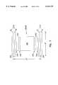
- FIGS. 4A and 4Billustrate a top view and a front view, respectively, of logic cells 205AA, 205BA, 205AB and 205BB having a split control line 210, e.g., A 1 and inverted A 1 .
- control lines 210are a general reference to the array 120, 130 input lines A 1 -A n and OL 1 -OL n , respectively.
- the advantage of split control linesis that only one transistor 200 is required per logic cell 205. Since the split control lines 210 are isolated from each other, this allows a single transistor to be selected.
- FIGS. 5A and SBillustrate a top view and a front view, respectively, of an alternative embodiment of logic cells 205AA and 205BA of FIG. 4A having a single control line, e.g., A 1 .
- a 1When single control line A 1 is high, the two transistors 200 on each side of the control line 210 are activated at the same time.
- the advantageis that there is redundancy in the selection of an output, but the drawback is the loss of circuit density because of the duplication.
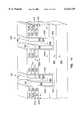
- FIG. 6Ais a perspective view illustrating generally one embodiment of a completed field programmable logic array 100, including portions of four transistors 200 having split control lines 210, such as illustrated in FIGS. 4A and 4B.
- the substantially identical transistorsare illustrated by way of example through logic cells 205AA, 205BA, 205AB and 205BB.
- Each logic cell 205includes a semiconductor pillar 300, initially of a first conductivity type such as P- silicon, fabricated upon a monolithic substrate 305.
- substrate 305is a bulk semiconductor, such as P- silicon.
- a semiconductor-on-insulator (SOI) substrate 305includes an insulating layer, such as silicon dioxide (SiO 2 ), as described below.
- Each pillar 300includes a first source/drain region of a second conductivity type, such as N+ silicon source region 310, formed proximally to a sub-micron dimensional interface between pillar 300 and substrate 305.
- Each pillar 300also includes a second source/drain region of the second conductivity type, such as N+ silicon drain region 315, that is distal to substrate 305, and separated from source region 3 1 0 by a first conductivity type region, such as P- body region 320.
- Each pillar 300provides a source region 310, a drain region 315, and a body region 320 for floating gate transistor 200 of a particular logic cell, e.g., 205AA.
- the physical dimensions of each pillar 300 and the doping of P- body region 320are both sufficiently small to allow operation of the floating gate transistors 200 that is characteristic of fully depleted body transistors.
- First source/drain region interconnection lines S 1 -S Nelectrically interconnects the source region 310 of each pillar 300 of cells.
- the first source/drain interconnection lines S 1 -S Ncomprise a conductively doped semiconductor of the second conductivity type, such as N+ silicon, disposed at least partially within substrate 305.
- dopantscan be ion-implanted or diffused into substrate 305 to form the first source/drain interconnection lines S 1 -S N .
- the first source/drain interconnection lines S 1 -S Nare formed above substrate 305.
- a doped epitaxial semiconductor layercan be grown on substrate 305, from which first source/drain interconnection lines S 1 -S N are formed.
- an undoped epitaxial semiconductor layercan be grown on substrate 305, and dopants then introduced by ion-implantation or diffusion to obtain the first source/drain interconnection lines S 1 -S N of the desired conductivity.
- Each pillar 300is outwardly formed from substrate 305, and is illustrated in FIG. 6A as extending vertically upward from substrate 305.
- Each pillar 300has a top region that is separated from substrate 305 by four surrounding side regions.
- a floating gate 202is formed substantially adjacent to two opposing side surfaces of pillar 300, and separated therefrom by a gate dielectric 330, such that there are two floating gates 202 per pillar 300, though FIG. 6A omits some of the floating gates 202 for clarity of illustration.
- Each floating gate 202has a corresponding substantially adjacent control line 210 from which it is separated by an intergate dielectric 340. Except at the periphery of array 100, there are two control lines 210 interposed between two approximately adjacent pillars 300.
- input A 1 and inverted A 1are interposed between logic zones 205AA, 205BA on one side and logic zones 205AB and 205BB on the other side.
- Input A 1controls logic zones 205AA and 205BA while inverted line input A 1 controls logic zones 205AB and 205BB.
- Input A 1 and inverted A 1are separated by an intergate dielectric 340.
- a single control line 210controls the two transistors 200 on each side of the control line, e.g., input A 1 .
- a logic cell 205has two transistors 200 operated from a single control line 210, as shown in FIG. 4B. This is in contrast to the split control line 210 embodiment where only one transistor 200 is operated by a single control line 210.
- Control lines 210are interposed between approximately adjacent pillars 300, wherein the input lines A 1 -A n are substantially parallel to each other.
- input lines A 1 -A nare illustrated as running in the Y-dimension, e.g. perpendicular to output lines OL 1 -OL n .
- Each of the input lines A 1 -A ninterconnects a plurality of transistors 200.
- input line A 1electrically interconnects the floating gate 202 of logic cells 205AA-205NA. Having split control lines 210 allows the floating gates 202 to be independent between pairs of logic cells, 205AA and 205AB, 205BA and 205BB, . . . , 205AN and 205BN.
- input lines A 1 -A nare disposed above substrate 305, as described below.
- Drain regions 315 of the pillars 300are interconnected by output lines OL 1 -OL n that are substantially parallel to each other in the X-dimension, e.g. perpendicular to input lines A 1 -A n .
- FIG. 6Aillustrates, by way of example, output lines OL n and OL n-1 , which are shown schematically for clarity. However, it is understood that output lines OL 1 -OL n comprise metal or other interconnection lines that are isolated from the underlying topology, e.g. pillars 300, floating gates 202, control lines A 1 -A n , and output lines OL 1 -OL n by an insulating layer through which contact holes are etched to access the drain regions 315 of the pillars 300.
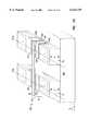
- FIG. 6Bis a cross-sectional view of FIG. 6A looking in the Y-dimension, e.g. perpendicular to output lines OL 1 -OL n .
- FIG. 6Billustrates a row of logic cells 205AA, 205AB, . . . , 205AN, having source regions 310 interconnected by one of first source/drain interconnection lines S 1 , S 2 , . . . , S N .
- FIG. 7is a plan view looking toward the working surface of substrate 305, illustrating generally by way of example one embodiment of logic cell 205AB.
- Each of the two floating gates 202is adjacent to one of opposing sides of pillar 300, and separated therefrom by gate dielectric 330.
- Each control line 210is separated from a corresponding floating gate 202 by an intergate dielectric 340.
- the control lines 210are likewise separated by intergate dielectric 340.
- Each control line 210is integrally formed together with one of the input lines A 1 -A n .
- the center-to-center spacing (“pitch") between control lines 210 that are on opposite sides of pillar 300is twice the minimum lithographic feature size F. Since two floating gate transistors 200 are contained within a logic cell 205 having an area of 4F 2 , an area of only 2F 2 is needed per logic cell.
- programming of one of the floating gate transistors 200is by hot electron injection.
- a voltage of approximately 10 voltsis provided to a particular one of input lines A 1 , A 2 , . . . , A n adjacent to a particular floating gate 200.
- a resulting inversion region (channel)is formed in the body region 320 at the surface that is approximately adjacent to the particular one of the input lines A 1 -A n .
- a voltage of approximately 10 Voltsis provided through a particular one of output lines OL 1 -OL n to a particular drain region 315.
- a voltage of approximately 0 Voltsis provided, through a particular one of first source/drain interconnection lines S 1 -S N , to the particular source region 310 of the floating gate transistor 200.
- Electronsare injected onto the floating gate 202 interposed between the control line 210 and the pillar 300 in which the particular drain region 315 is disposed.
- the exact value of the voltages provided to the particular control line 210 and drain region 315will depend on the physical dimension of the floating gate transistor 200, including the thickness of the gate dielectric 330, the thickness of the intergate dielectric 340, and the separation between source region 310 and drain region 315.
- the floating gate transistor 200may be programmed instead by Fowler-Nordheim tunneling of electrons from the body region 320, source region 310, or drain region 315.
- reading data stored on a particular floating gate transistor 200includes providing a voltage of approximately 5 volts through a particular one of the input lines A 1 , A 2 , . . . , A n to a particular control line 210 of the floating gate transistor 200.
- a voltage of approximately 0 Voltsis provided common ground S 1 , S 2 , . . . , S N to the particular source region 310 of the particular floating gate transistor 200.
- a particular one of output lines OL 1 -OL n that is switchably coupled to the drain region 315 of the floating gate transistor 200is precharged to a positive voltage by a pull up transistor, then coupled to the drain region 315 to determine the conductivity state of the floating gate transistor 200 between its source region 310 and drain region 315.
- the floating gate transistor 200will conduct between its source region 310 and drain region 315, decreasing the voltage of the particular one of output lines OL 1 -OL n toward that voltage of its source region 310, e.g. toward a "low" binary logic level voltage of approximately 0 Volts. If there are electrons stored on the floating gate 202, the floating gate transistor 200 will not conduct between its source region 310 and drain region 315. As a result, pull up transistor 240 will tend to increase the voltage of the particular one of output lines OL 1 -OL n toward a positive voltage, e.g. toward a "high" binary logic voltage level.
- erasure of floating gate transistors 200includes providing an erasure voltage difference of approximately between 10 and 12 Volts from a source region 310 to a corresponding control line 210.
- a voltage of approximately 0 Voltsis provided to source regions 310 of floating gate transistors 200 that are interconnected by one or several first source/drain interconnection lines S 1 , S 2 , . . . , S N .
- a voltage of approximately between 10 and 12 Voltsis provided through a corresponding one or several of the input lines A 1 -A n to the control lines 210 of the floating gate transistors 200 to be erased.
- the negative voltage applied to the control lines 210electrons are removed from the corresponding floating gates 202 by Fowler-Nordheim tunneling, thereby removing the charge from one of the floating gate transistors 200.
- a voltage of approximately between -5 and -6 Voltsis applied to the control lines 210 and a voltage of approximately between +5 and +6 Volts is applied to the source regions 310 in order to obtain the erasure voltage difference of approximately between -10 and -12 Volts from a source region 310 to a corresponding control line 210.
- the exact value of the erasure voltage differencewill vary depending upon the physical dimensions of the floating gate transistor 200 and the thicknesses of gate dielectric 330 and intergate dielectric 340.
- an entire row of floating gate transistors 200is simultaneously erased by applying approximately between -10 and -12 Volts to each of inputs A 1 -A n , and also applying 0 Volts to each of first source/drain interconnection lines S 1 , S 2 , . . . , S N .
- one or more sectors of a roware simultaneously erased by selectively applying approximately between -10 and -12 Volts to one or more of input lines A 1 -A n and also applying 0 Volts to one or more of first source/drain interconnection lines S 1 , S 2 , . . . , S N .
- FIGS. 8-16illustrate generally one embodiment of a method of forming field programmable logic array 100.
- field programmable logic array 100is formed using bulk silicon processing techniques and is described, by way of example, with respect to a particular technology having a minimum lithographic feature size F, which is also sometimes referred to as a critical dimension (CD), of 0.4 microns.
- CDcritical dimension
- the process steps described belowcan be scaled accordingly for other minimum feature sizes without departing from the scope of the invention.
- horizontalas used in this application is defined as a plane parallel to the conventional plane or surface of a wafer or substrate, regardless of the orientation of the wafer or the substrate.
- verticalrefers to a dimension perpendicular to the horizontal as defined above. Prepositions, such as “on,” “side,” (as in sidewall), “higher,” “lower,” “over,” and under are defined with respect to the conventional plane or surface being on the top surface of the wafer or substrate, regardless of the orientation of the wafer or substrate.
- a P- silicon starting materialis used for substrate 305.
- a first source/drain layer 500of approximate thickness between 0.2 microns and 0.5 microns, is formed at a working surface of substrate 305.
- first source/drain layer 500is N+ silicon formed by ion-implantation of donor dopants into substrate 305.
- first source/drain layer 500is N+ silicon formed by epitaxial growth of silicon upon substrate 305.
- a semiconductor epitaxial layer 505such as P- silicon of 0.6 micron approximate thickness, is formed, such as by epitaxial growth.
- a second source/drain layer 510such as N+ silicon of 150 nanometers approximate thickness, is formed at a surface of the epitaxial layer 505, such as by ion-implantation of donor dopants into P- epitaxial layer 505 or by epitaxial growth of N+ silicon on P- epitaxial layer 505.
- Pad oxide 515has a thickness of approximately 10 nanometers.
- Pad nitride 520has a thickness of approximately 100 nanometers.
- photoresist masking and selective etching techniquesare used to form, in the first dimension (e.g., the Y-dimension, which is perpendicular to the plane of the drawing of FIG. 9), a plurality of substantially parallel first troughs 600 that extend through the pad nitride 520, pad oxide 515, second source/drain layer 510, the underlying portion of epitaxial layer 505, first source/drain layer 500, and at least partially into underlying P- silicon substrate 305.
- the photoresistis then removed by conventional photoresist stripping techniques, and an insulator 605, such as silicon dioxide deposited by chemical vapor deposition (CVD), is formed to fill first troughs 600.
- the insulator 605is planarized (e.g. exposing underlying portions of pad nitride 520) such as by chemical mechanical polishing (CMP) or other suitable planarization technique.
- a masking layer 610such as, for example, silicon nitride deposited by CVD and having an approximate thickness of 200 nanometers, is then formed on insulator 605 and elsewhere on the working surface of substrate 305.
- a photoresist layer 615is then formed on masking layer 610.
- FIG. 1Ois a perspective view, illustrating the selective etching, in a second dimension (X-dimension) that is substantially orthogonal to the first dimension (Y-dimension), of a plurality of substantially parallel second troughs 700, as described below.
- Forming second troughs 700includes patterning photoresist layer 615, selectively etching masking layer 610, pad nitride 520, and underlying pad oxide 515, such that portions of silicon dioxide insulator 605 in the second troughs 700 are exposed, together with N+ silicon second source/drain layer 510.
- a selective etchwhich preferentially removes silicon but doesn't substantially remove silicon dioxide, is used to etch through the exposed portions of second source/drain layer 510, the underlying portions of epitaxial layer 505, and approximately 100 nanometers into the underlying portions of first source/drain layer 500.
- Photorcsist 615is then removed by conventional photoresist stripping techniques, leaving the structure illustrated in FIG. 10.
- FIG. 11is a cross-sectional view looking in the direction of second troughs 700 (e.g. such that the X-dimension is orthogonal to the plane of the illustration of FIG. 11).
- a thin oxidation barrier layer 900such as silicon nitride of approximate thickness of 20 nanometers, is conformally deposited by CVD to protect against the oxidation of sidewalls of second troughs 700.
- Barrier layer 900is anisotropically etched to expose bottom portions of second troughs 700.
- a bottom insulation layer 905is formed on the bottoms of second troughs 700, such as silicon dioxide of approximate thickness of 100 nanometers formed by thermal oxidation of the exposed bottom portions of second troughs 700.
- barrier layer 900is stripped from the sidewalls of the second troughs 700, such as by a brief phosphoric acid etch, which is timed to expose the sidewalls of the second troughs 700 but which avoids significant removal of the thick silicon nitride masking layer 610.
- a gate dielectric layer 1000such as silicon dioxide of thickness approximately between 5 nanometers and 10 nanometers (sometimes referred to as "tunnel oxide”), is formed substantially adjacent to the exposed sidewalls of the second troughs 700.
- a conductive layer 1005, such as N+ doped polysilicon,is formed in the second troughs 700, such as by CVD, to fill the second troughs 700.
- the conductive layer 1005is planarized, such as by chemical mechanical polishing (CMP) or other suitable planarization technique.
- CMPchemical mechanical polishing
- the conductive layer 1005is etched back in the second troughs 700 to approximately at or slightly above the level of the silicon surface, which is defined by the interface between the second source/drain layer 510 and the pad oxide 515 layer.
- a spacer layersuch as silicon nitride of an approximate thickness of 100 nanometers, is deposited by CVD and anisotropically etched by reactive ion etching (RIE) to leave nitride spacers 1100 along the sidewalls of the second troughs 700, e.g. on the etched back portions of the conductive layer 1005, on the portions of insulator 605 in the intersections of first troughs 600 and second troughs 700, and against the second gate dielectric 1000.
- RIEreactive ion etching
- spacers 1100are used as a mask for the anisotropic etching in the second troughs 700 of the etched back portions of polysilicon conductive layer 1005 and the portions of silicon dioxide insulator 605.
- a selective etchwhich preferentially removes silicon dioxide but doesn't substantially remove polysilicon, is used to etch into portions of silicon dioxide insulator 605, but not the portions of polysilicon conductive layer 1005 in second troughs 700.
- the portions of silicon dioxide insulator 605 in second troughs 700are etched until they are approximately even with adjacent portions of bottom insulating layer 905. Then, a selective etch, which preferentially removes polysilicon but doesn't substantially remove silicon dioxide, is used to etch through portions of conductive layer 1005 in second troughs until the bottom insulation layer 905 is exposed, thereby forming from the polysilicon conductive layer 1005 separate floating gates 202 along the sidewalls of the second troughs 700.
- an intergate dielectric 1300is formed in the second troughs 700, such that the intergate dielectric 1300 has an approximate thickness between 7 nanometers and 15 nanometers.
- formation of intergate dielectric 1300is by thermal growth of silicon dioxide.
- formation of intergate dielectric 1300is by deposition of oxynitride by CVD.
- Single control line 210are formed between opposing floating gates 202 in the second troughs 700 and separated therefrom by the intergate dielectric 1300.
- the control lines 210 in second troughs 700are formed together with the output lines OL 1 -OL n in second troughs 700 by a single deposition greater than 150 nanometers of N+ doped polysilicon that fills second troughs 700 and is planarized, such as by CMP down to the top level of silicon nitride masking layer 610.
- Split control lines 210are formed between opposing floating gates 202 in the second troughs 700 and separated therefrom by the intergate dielectric 1300.
- the control lines 210 in second troughs 700are formed together with the output lines OL 1 -OL n in second troughs 700 by a single deposition of approximately 70 nanometers of N+ doped polysilicon that is then directionally etched to leave on vertical services only as separated conducting lines.
- Phosphoric acidis used to remove the remaining silicon nitride, such as spacers 1100, masking layer 610, and pad nitride 520, leaving the structure illustrated in FIG. 15.
- An insulatorsuch as silicon dioxide is then deposited, and subsequent processing follows conventional techniques for forming contact holes, terminal metal, and inter level insulator steps to complete wiring of the cells 205 and other circuits of field programmable logic array 100.
- FIGS. 8-16illustrate generally one embodiment of forming the memory array 105 using bulk silicon processing techniques
- a semiconductor-on-insulator (SOI) substrateis formed from substrate 305.
- a P- silicon starting materialis used for substrate 305, and processing begins similarly to the bulk semiconductor embodiment described in FIG. 8.
- an oxidation barrier layeris formed on the sidewalls of the first troughs 600.
- An isotropic chemical etchis used to fully undercut the semiconductor regions separating the first troughs 600, and a subsequent oxidation step is used to fill in the evacuated regions formed by the undercutting.
- substrate 305is understood to include bulk semiconductor as well as SOI embodiments in which the semiconductor integrated circuits formed on the surface of substrate 305 are isolated from each other and an underlying semiconductor portion of substrate 305 by an insulating layer.
- the present inventionprovides a high density field programmable logic array 100 that is easily programmed for selecting functional logic outputs based upon preselected inputs. Programmability is achieved with a field-effect transistor (FET) having an electrically isolated (floating) gate that controls electrical conduction between source regions and drain regions. Programmability is accomplished without having to mask the desired logic functions into an array structure.
- FETfield-effect transistor
- the floating gate transistor 200only needs an area of only 2F 2 to store a single bit of logic data.
Landscapes
- Physics & Mathematics (AREA)
- Mathematical Physics (AREA)
- Engineering & Computer Science (AREA)
- Computer Hardware Design (AREA)
- Computing Systems (AREA)
- General Engineering & Computer Science (AREA)
- Logic Circuits (AREA)
Abstract
Description
Claims (35)
Priority Applications (3)
| Application Number | Priority Date | Filing Date | Title |
|---|---|---|---|
| US09/032,617US6124729A (en) | 1998-02-27 | 1998-02-27 | Field programmable logic arrays with vertical transistors |
| US09/520,494US6486027B1 (en) | 1998-02-27 | 2000-03-08 | Field programmable logic arrays with vertical transistors |
| US10/230,244US6812516B2 (en) | 1998-02-27 | 2002-08-28 | Field programmable logic arrays with vertical transistors |
Applications Claiming Priority (1)
| Application Number | Priority Date | Filing Date | Title |
|---|---|---|---|
| US09/032,617US6124729A (en) | 1998-02-27 | 1998-02-27 | Field programmable logic arrays with vertical transistors |
Related Child Applications (1)
| Application Number | Title | Priority Date | Filing Date |
|---|---|---|---|
| US09/520,494DivisionUS6486027B1 (en) | 1998-02-27 | 2000-03-08 | Field programmable logic arrays with vertical transistors |
Publications (1)
| Publication Number | Publication Date |
|---|---|
| US6124729Atrue US6124729A (en) | 2000-09-26 |
Family
ID=21865886
Family Applications (3)
| Application Number | Title | Priority Date | Filing Date |
|---|---|---|---|
| US09/032,617Expired - LifetimeUS6124729A (en) | 1998-02-27 | 1998-02-27 | Field programmable logic arrays with vertical transistors |
| US09/520,494Expired - LifetimeUS6486027B1 (en) | 1998-02-27 | 2000-03-08 | Field programmable logic arrays with vertical transistors |
| US10/230,244Expired - Fee RelatedUS6812516B2 (en) | 1998-02-27 | 2002-08-28 | Field programmable logic arrays with vertical transistors |
Family Applications After (2)
| Application Number | Title | Priority Date | Filing Date |
|---|---|---|---|
| US09/520,494Expired - LifetimeUS6486027B1 (en) | 1998-02-27 | 2000-03-08 | Field programmable logic arrays with vertical transistors |
| US10/230,244Expired - Fee RelatedUS6812516B2 (en) | 1998-02-27 | 2002-08-28 | Field programmable logic arrays with vertical transistors |
Country Status (1)
| Country | Link |
|---|---|
| US (3) | US6124729A (en) |
Cited By (64)
| Publication number | Priority date | Publication date | Assignee | Title |
|---|---|---|---|---|
| US6351428B2 (en) | 2000-02-29 | 2002-02-26 | Micron Technology, Inc. | Programmable low voltage decode circuits with ultra-thin tunnel oxides |
| US6377070B1 (en) | 2001-02-09 | 2002-04-23 | Micron Technology, Inc. | In-service programmable logic arrays with ultra thin vertical body transistors |
| US6380765B1 (en)* | 2000-08-29 | 2002-04-30 | Micron Technology, Inc. | Double pass transistor logic with vertical gate transistors |
| US6420902B1 (en)* | 2000-05-31 | 2002-07-16 | Micron Technology, Inc. | Field programmable logic arrays with transistors with vertical gates |
| US6424001B1 (en) | 2001-02-09 | 2002-07-23 | Micron Technology, Inc. | Flash memory with ultra thin vertical body transistors |
| US20020164853A1 (en)* | 2000-08-22 | 2002-11-07 | Micron Technology, Inc. | Vertical gate transistors in pass transistor programmable logic arrays |
| US20030042528A1 (en)* | 2001-08-30 | 2003-03-06 | Leonard Forbes | Sram cells with repressed floating gate memory, low tunnel barrier interpoly insulators |
| US20030048666A1 (en)* | 2001-08-30 | 2003-03-13 | Micron Technology, Inc. | Graded composition metal oxide tunnel barrier interpoly insulators |
| US6566682B2 (en) | 2001-02-09 | 2003-05-20 | Micron Technology, Inc. | Programmable memory address and decode circuits with ultra thin vertical body transistors |
| US20030107402A1 (en)* | 2001-02-09 | 2003-06-12 | Micron Technology, Inc. | Programmable logic arrays with ultra thin body transistors |
| US6605961B1 (en)* | 2000-02-29 | 2003-08-12 | Micron Technology, Inc. | Low voltage PLA's with ultrathin tunnel oxides |
| US6639835B2 (en) | 2000-02-29 | 2003-10-28 | Micron Technology, Inc. | Static NVRAM with ultra thin tunnel oxides |
| US20030218199A1 (en)* | 2001-02-09 | 2003-11-27 | Micron Technology, Inc. | Open bit line DRAM with ultra-thin body transistors |
| US20030234420A1 (en)* | 2002-06-21 | 2003-12-25 | Micron Technology, Inc. | Write once read only memory with large work function floating gates |
| US20030235079A1 (en)* | 2002-06-21 | 2003-12-25 | Micron Technology, Inc. | Nor flash memory cell with high storage density |
| US20040007721A1 (en)* | 2001-02-09 | 2004-01-15 | Micron Technology, Inc. | Folded bit line DRAM with vertical ultra thin body transistors |
| US20040042256A1 (en)* | 2002-08-29 | 2004-03-04 | Micron Technology, Inc. | Single transistor vertical memory gain cell |
| US20040041236A1 (en)* | 2002-08-29 | 2004-03-04 | Micron Technology, Inc. | Merged mos-bipolar capacitor memory cell |
| US6744094B2 (en) | 2001-08-24 | 2004-06-01 | Micron Technology Inc. | Floating gate transistor with horizontal gate layers stacked next to vertical body |
| US20040108532A1 (en)* | 2002-12-04 | 2004-06-10 | Micron Technology, Inc. | Embedded DRAM gain memory cell |
| US6754108B2 (en) | 2001-08-30 | 2004-06-22 | Micron Technology, Inc. | DRAM cells with repressed floating gate memory, low tunnel barrier interpoly insulators |
| US20040130934A1 (en)* | 2002-06-21 | 2004-07-08 | Micron Technology, Inc. | NROM memory cell, memory array, related devices and methods |
| US20040168145A1 (en)* | 2001-08-30 | 2004-08-26 | Micron Technology, Inc. | Service programmable logic arrays with low tunnel barrier interpoly insulators |
| US6804136B2 (en) | 2002-06-21 | 2004-10-12 | Micron Technology, Inc. | Write once read only memory employing charge trapping in insulators |
| US6804142B2 (en) | 2002-11-12 | 2004-10-12 | Micron Technology, Inc. | 6F2 3-transistor DRAM gain cell |
| US6838726B1 (en) | 2000-05-31 | 2005-01-04 | Micron Technology, Inc. | Horizontal memory devices with vertical gates |
| US6842369B2 (en) | 2002-05-07 | 2005-01-11 | Hewlett-Packard Development Company, L.P. | Intermesh memory device |
| US20050009354A1 (en)* | 2003-07-11 | 2005-01-13 | Kwan-Ju Koh | MOS transistor and fabrication method thereof |
| US20050012141A1 (en)* | 2002-02-12 | 2005-01-20 | Micron Technology, Inc. | Asymmetric band-gap engineered nonvolatile memory device |
| US20050023602A1 (en)* | 2001-08-30 | 2005-02-03 | Micron Technology, Inc. | Programmable array logic or memory with p-channel devices and asymmetrical tunnel barriers |
| US20050024936A1 (en)* | 2003-03-04 | 2005-02-03 | Micron Technology, Inc. | Vertical gain cell |
| US20050023595A1 (en)* | 2001-08-30 | 2005-02-03 | Micron Technology, Inc. | Programmable array logic or memory devices with asymmetrical tunnel barriers |
| US20050128804A1 (en)* | 2003-12-16 | 2005-06-16 | Micron Technology, Inc. | Multi-state NROM device |
| US6937513B1 (en)* | 2003-10-16 | 2005-08-30 | Lsi Logic Corporation | Integrated NAND and nor-type flash memory device and method of using the same |
| US20060002192A1 (en)* | 2001-08-30 | 2006-01-05 | Micron Technology | Integrated circuit memory device and method |
| US20060028869A1 (en)* | 2004-08-03 | 2006-02-09 | Micron Technology, Inc. | High density stepped, non-planar flash memory |
| US20060128104A1 (en)* | 2003-12-16 | 2006-06-15 | Micron Technology, Inc. | NROM memory cell, memory array, related devices and methods |
| US7068544B2 (en) | 2001-08-30 | 2006-06-27 | Micron Technology, Inc. | Flash memory with low tunnel barrier interpoly insulators |
| US7075829B2 (en) | 2001-08-30 | 2006-07-11 | Micron Technology, Inc. | Programmable memory address and decode circuits with low tunnel barrier interpoly insulators |
| US20060170032A1 (en)* | 2001-08-30 | 2006-08-03 | Micron Technology, Inc. | Scalable Flash/NV structures and devices with extended endurance |
| US7130220B2 (en) | 2002-06-21 | 2006-10-31 | Micron Technology, Inc. | Write once read only memory employing floating gates |
| US20060273370A1 (en)* | 2005-06-07 | 2006-12-07 | Micron Technology, Inc. | NROM flash memory with vertical transistors and surrounding gates |
| US20060278926A1 (en)* | 2005-06-08 | 2006-12-14 | Suraj Mathew | Capacitorless DRAM on bulk silicon |
| US20060279329A1 (en)* | 2005-05-19 | 2006-12-14 | Infineon Technologies Ag | Mask-programmable logic macro and method for programming a logic macro |
| US7151024B1 (en) | 2004-09-02 | 2006-12-19 | Micron Technology, Inc. | Long retention time single transistor vertical memory gain cell |
| US7221586B2 (en) | 2002-07-08 | 2007-05-22 | Micron Technology, Inc. | Memory utilizing oxide nanolaminates |
| US7221017B2 (en) | 2002-07-08 | 2007-05-22 | Micron Technology, Inc. | Memory utilizing oxide-conductor nanolaminates |
| US7271052B1 (en) | 2004-09-02 | 2007-09-18 | Micron Technology, Inc. | Long retention time single transistor vertical memory gain cell |
| US7271433B1 (en) | 2004-09-02 | 2007-09-18 | Micron Technology, Inc. | High-density single transistor vertical memory gain cell |
| US7429515B2 (en) | 2001-12-20 | 2008-09-30 | Micron Technology, Inc. | Low-temperature grown high quality ultra-thin CoTiO3 gate dielectrics |
| US7446368B2 (en) | 2001-08-30 | 2008-11-04 | Micron Technology, Inc. | Deposition of metal oxide and/or low asymmetrical tunnel barrier interpoly insulators |
| US20080316828A1 (en)* | 2007-06-21 | 2008-12-25 | Hanafi Hussein I | Memory in logic cell |
| US20080315917A1 (en)* | 2007-06-21 | 2008-12-25 | Micron Technology, Inc. | Programmable computing array |
| US7489545B2 (en) | 2002-07-08 | 2009-02-10 | Micron Technology, Inc. | Memory utilizing oxide-nitride nanolaminates |
| US7560793B2 (en) | 2002-05-02 | 2009-07-14 | Micron Technology, Inc. | Atomic layer deposition and conversion |
| US20090261415A1 (en)* | 2008-04-17 | 2009-10-22 | Adkisson James W | Fully-depleted low-body doping field effect transistor (fet) with reverse short channel effects (sce) induced by self-aligned edge back-gate(s) |
| US7670646B2 (en) | 2002-05-02 | 2010-03-02 | Micron Technology, Inc. | Methods for atomic-layer deposition |
| US7709402B2 (en) | 2006-02-16 | 2010-05-04 | Micron Technology, Inc. | Conductive layers for hafnium silicon oxynitride films |
| US20110169064A1 (en)* | 2010-01-11 | 2011-07-14 | International Business Machines Corporation | Read transistor for single poly non-volatile memory using body contacted soi device |
| US8501563B2 (en) | 2005-07-20 | 2013-08-06 | Micron Technology, Inc. | Devices with nanocrystals and methods of formation |
| US20150123182A1 (en)* | 2013-11-01 | 2015-05-07 | SK Hynix Inc. | Transistor and semiconductor device including the same |
| US9281065B2 (en) | 2014-08-11 | 2016-03-08 | Empire Technology Development Llc | Low-power nonvolatile memory cells with select gates |
| USRE48941E1 (en)* | 2007-11-07 | 2022-02-22 | Sony Group Corporation | Semiconductor integrated circuit |
| US20220059667A1 (en)* | 2020-08-24 | 2022-02-24 | Micron Technology, Inc. | Integrated Assemblies Containing Ferroelectric Transistors, and Methods of Forming Integrated Assemblies |
Families Citing this family (34)
| Publication number | Priority date | Publication date | Assignee | Title |
|---|---|---|---|---|
| US6066869A (en) | 1997-10-06 | 2000-05-23 | Micron Technology, Inc. | Circuit and method for a folded bit line memory cell with vertical transistor and trench capacitor |
| US6025225A (en) | 1998-01-22 | 2000-02-15 | Micron Technology, Inc. | Circuits with a trench capacitor having micro-roughened semiconductor surfaces and methods for forming the same |
| KR100821456B1 (en) | 2000-08-14 | 2008-04-11 | 샌디스크 쓰리디 엘엘씨 | Dense array and charge storage device and manufacturing method thereof |
| US8026161B2 (en) | 2001-08-30 | 2011-09-27 | Micron Technology, Inc. | Highly reliable amorphous high-K gate oxide ZrO2 |
| US6891256B2 (en)* | 2001-10-22 | 2005-05-10 | Fairchild Semiconductor Corporation | Thin, thermally enhanced flip chip in a leaded molded package |
| US6680508B1 (en)* | 2002-08-28 | 2004-01-20 | Micron Technology, Inc. | Vertical floating gate transistor |
| US6794699B2 (en)* | 2002-08-29 | 2004-09-21 | Micron Technology Inc | Annular gate and technique for fabricating an annular gate |
| US7192892B2 (en) | 2003-03-04 | 2007-03-20 | Micron Technology, Inc. | Atomic layer deposited dielectric layers |
| US7276754B2 (en)* | 2003-08-29 | 2007-10-02 | Micron Technology, Inc. | Annular gate and technique for fabricating an annular gate |
| DE10350751B4 (en)* | 2003-10-30 | 2008-04-24 | Infineon Technologies Ag | Method for producing a vertical field effect transistor and field effect memory transistor, in particular FLASH memory transistor |
| US7202523B2 (en) | 2003-11-17 | 2007-04-10 | Micron Technology, Inc. | NROM flash memory devices on ultrathin silicon |
| US7081421B2 (en) | 2004-08-26 | 2006-07-25 | Micron Technology, Inc. | Lanthanide oxide dielectric layer |
| US7494939B2 (en) | 2004-08-31 | 2009-02-24 | Micron Technology, Inc. | Methods for forming a lanthanum-metal oxide dielectric layer |
| US7374964B2 (en) | 2005-02-10 | 2008-05-20 | Micron Technology, Inc. | Atomic layer deposition of CeO2/Al2O3 films as gate dielectrics |
| US7662729B2 (en) | 2005-04-28 | 2010-02-16 | Micron Technology, Inc. | Atomic layer deposition of a ruthenium layer to a lanthanide oxide dielectric layer |
| US7420248B2 (en)* | 2005-08-25 | 2008-09-02 | International Business Machines Corporation | Programmable random logic arrays using PN isolation |
| KR100657969B1 (en) | 2005-08-30 | 2006-12-14 | 삼성전자주식회사 | A manufacturing method of a semiconductor device having a single gate electrode corresponding to a pair of pin-type channel regions |
| US7410910B2 (en) | 2005-08-31 | 2008-08-12 | Micron Technology, Inc. | Lanthanum aluminum oxynitride dielectric films |
| US8071476B2 (en) | 2005-08-31 | 2011-12-06 | Micron Technology, Inc. | Cobalt titanium oxide dielectric films |
| US7644385B1 (en) | 2005-11-07 | 2010-01-05 | Altera Corporation | Programmable logic device with performance variation compensation |
| KR20080051014A (en)* | 2006-12-04 | 2008-06-10 | 삼성전자주식회사 | And-type and Noah-type Flash Memory Arrays with Vertical Structures and Their Manufacturing and Operation Methods |
| US7646041B2 (en)* | 2006-12-04 | 2010-01-12 | Samsung Electronics Co., Ltd. | Non-volatile memory devices including vertical channels, methods of operating, and methods of fabricating the same |
| US7759237B2 (en)* | 2007-06-28 | 2010-07-20 | Micron Technology, Inc. | Method of forming lutetium and lanthanum dielectric structures |
| KR20100007229A (en)* | 2008-07-11 | 2010-01-22 | 삼성전자주식회사 | Non-volatile memory device and method of fabricating the same |
| US8630114B2 (en)* | 2011-01-19 | 2014-01-14 | Macronix International Co., Ltd. | Memory architecture of 3D NOR array |
| US9214351B2 (en) | 2013-03-12 | 2015-12-15 | Macronix International Co., Ltd. | Memory architecture of thin film 3D array |
| US9627395B2 (en) | 2015-02-11 | 2017-04-18 | Sandisk Technologies Llc | Enhanced channel mobility three-dimensional memory structure and method of making thereof |
| US9478495B1 (en) | 2015-10-26 | 2016-10-25 | Sandisk Technologies Llc | Three dimensional memory device containing aluminum source contact via structure and method of making thereof |
| US11737274B2 (en) | 2021-02-08 | 2023-08-22 | Macronix International Co., Ltd. | Curved channel 3D memory device |
| US11916011B2 (en) | 2021-04-14 | 2024-02-27 | Macronix International Co., Ltd. | 3D virtual ground memory and manufacturing methods for same |
| US11710519B2 (en) | 2021-07-06 | 2023-07-25 | Macronix International Co., Ltd. | High density memory with reference memory using grouped cells and corresponding operations |
| US12299597B2 (en) | 2021-08-27 | 2025-05-13 | Macronix International Co., Ltd. | Reconfigurable AI system |
| US12321603B2 (en) | 2023-02-22 | 2025-06-03 | Macronix International Co., Ltd. | High bandwidth non-volatile memory for AI inference system |
| US12417170B2 (en) | 2023-05-10 | 2025-09-16 | Macronix International Co., Ltd. | Computing system and method of operation thereof |
Citations (88)
| Publication number | Priority date | Publication date | Assignee | Title |
|---|---|---|---|---|
| US3931617A (en)* | 1974-10-07 | 1976-01-06 | Signetics Corporation | Collector-up dynamic memory cell |
| US4020364A (en)* | 1974-09-28 | 1977-04-26 | U.S. Philips Corporation | Resistance read amplifier |
| US4051354A (en)* | 1975-07-03 | 1977-09-27 | Texas Instruments Incorporated | Fault-tolerant cell addressable array |
| US4313106A (en)* | 1980-06-30 | 1982-01-26 | Rca Corporation | Electrically programmable logic array |
| JPS61140170A (en)* | 1984-12-13 | 1986-06-27 | Toshiba Corp | semiconductor storage device |
| US4604162A (en)* | 1983-06-13 | 1986-08-05 | Ncr Corporation | Formation and planarization of silicon-on-insulator structures |
| US4617649A (en)* | 1981-11-17 | 1986-10-14 | Ricoh Company, Ltd. | Erasable FPLA |
| US4630088A (en)* | 1984-09-11 | 1986-12-16 | Kabushiki Kaisha Toshiba | MOS dynamic ram |
| US4663831A (en)* | 1985-10-08 | 1987-05-12 | Motorola, Inc. | Method of forming transistors with poly-sidewall contacts utilizing deposition of polycrystalline and insulating layers combined with selective etching and oxidation of said layers |
| US4673962A (en)* | 1985-03-21 | 1987-06-16 | Texas Instruments Incorporated | Vertical DRAM cell and method |
| US4677589A (en)* | 1985-07-26 | 1987-06-30 | Advanced Micro Devices, Inc. | Dynamic random access memory cell having a charge amplifier |
| US4761768A (en)* | 1985-03-04 | 1988-08-02 | Lattice Semiconductor Corporation | Programmable logic device |
| US4766569A (en)* | 1985-03-04 | 1988-08-23 | Lattice Semiconductor Corporation | Programmable logic array |
| US4888735A (en)* | 1987-12-30 | 1989-12-19 | Elite Semiconductor & Systems Int'l., Inc. | ROM cell and array configuration |
| US4906590A (en)* | 1988-05-09 | 1990-03-06 | Mitsubishi Denki Kabushiki Kaisha | Method of forming a trench capacitor on a semiconductor substrate |
| US4920065A (en)* | 1988-10-31 | 1990-04-24 | International Business Machines Corporation | Method of making ultra dense dram cells |
| US4920515A (en)* | 1987-10-23 | 1990-04-24 | Ricoh Company, Ltd. | Programmable logic array having an improved testing arrangement |
| US4958318A (en)* | 1988-07-08 | 1990-09-18 | Eliyahou Harari | Sidewall capacitor DRAM cell |
| US4987089A (en)* | 1990-07-23 | 1991-01-22 | Micron Technology, Inc. | BiCMOS process and process for forming bipolar transistors on wafers also containing FETs |
| US5001526A (en)* | 1987-11-10 | 1991-03-19 | Fujitsu Limited | Dram cell formed on an insulating layer having a buried semiconductor pillar structure and a manufacturing method thereof |
| US5006909A (en)* | 1989-10-30 | 1991-04-09 | Motorola, Inc. | Dram with a vertical capacitor and transistor |
| US5017504A (en)* | 1986-12-01 | 1991-05-21 | Mitsubishi Denki Kabushiki Kaisha | Vertical type MOS transistor and method of formation thereof |
| US5021355A (en)* | 1989-05-22 | 1991-06-04 | International Business Machines Corporation | Method of fabricating cross-point lightly-doped drain-source trench transistor |
| US5028977A (en)* | 1989-06-16 | 1991-07-02 | Massachusetts Institute Of Technology | Merged bipolar and insulated gate transistors |
| US5057896A (en)* | 1988-05-28 | 1991-10-15 | Fujitsu Limited | Semiconductor device and method of producing same |
| US5072269A (en)* | 1988-03-15 | 1991-12-10 | Kabushiki Kaisha Toshiba | Dynamic ram and method of manufacturing the same |
| US5102817A (en)* | 1985-03-21 | 1992-04-07 | Texas Instruments Incorporated | Vertical DRAM cell and method |
| US5107459A (en)* | 1990-04-20 | 1992-04-21 | International Business Machines Corporation | Stacked bit-line architecture for high density cross-point memory cell array |
| US5110752A (en)* | 1991-07-10 | 1992-05-05 | Industrial Technology Research Institute | Roughened polysilicon surface capacitor electrode plate for high denity dram |
| US5156987A (en)* | 1991-12-18 | 1992-10-20 | Micron Technology, Inc. | High performance thin film transistor (TFT) by solid phase epitaxial regrowth |
| US5177028A (en)* | 1991-10-22 | 1993-01-05 | Micron Technology, Inc. | Trench isolation method having a double polysilicon gate formed on mesas |
| US5177576A (en)* | 1990-05-09 | 1993-01-05 | Hitachi, Ltd. | Dynamic random access memory having trench capacitors and vertical transistors |
| US5191509A (en)* | 1991-12-11 | 1993-03-02 | International Business Machines Corporation | Textured polysilicon stacked trench capacitor |
| US5202278A (en)* | 1991-09-10 | 1993-04-13 | Micron Technology, Inc. | Method of forming a capacitor in semiconductor wafer processing |
| US5208657A (en)* | 1984-08-31 | 1993-05-04 | Texas Instruments Incorporated | DRAM Cell with trench capacitor and vertical channel in substrate |
| US5216266A (en)* | 1990-04-11 | 1993-06-01 | Mitsubishi Denki Kabushiki Kaisha | Semiconductor memory device having memory cells formed in trench and manufacturing method therefor |
| US5223081A (en)* | 1991-07-03 | 1993-06-29 | Doan Trung T | Method for roughening a silicon or polysilicon surface for a semiconductor substrate |
| JPH05226661A (en)* | 1992-02-17 | 1993-09-03 | Mitsubishi Electric Corp | Semiconductor device and manufacturing method thereof |
| US5266514A (en)* | 1992-12-21 | 1993-11-30 | Industrial Technology Research Institute | Method for producing a roughened surface capacitor |
| US5276343A (en)* | 1990-04-21 | 1994-01-04 | Kabushiki Kaisha Toshiba | Semiconductor memory device having a bit line constituted by a semiconductor layer |
| US5316962A (en)* | 1989-08-15 | 1994-05-31 | Matsushita Electric Industrial Co., Ltd. | Method of producing a semiconductor device having trench capacitors and vertical switching transistors |
| US5320880A (en)* | 1992-10-20 | 1994-06-14 | Micron Technology, Inc. | Method of providing a silicon film having a roughened outer surface |
| US5327380A (en)* | 1988-10-31 | 1994-07-05 | Texas Instruments Incorporated | Method and apparatus for inhibiting a predecoder when selecting a redundant row line |
| US5329481A (en)* | 1991-12-16 | 1994-07-12 | U.S. Philips Corporation | Semiconductor device having a memory cell |
| US5341331A (en)* | 1991-07-31 | 1994-08-23 | Samsung Electronics, Co., Ltd. | Data transmission circuit having common input/output lines |
| US5376575A (en)* | 1991-09-26 | 1994-12-27 | Hyundai Electronics Industries, Inc. | Method of making dynamic random access memory having a vertical transistor |
| US5378914A (en)* | 1990-05-31 | 1995-01-03 | Canon Kabushiki Kaisha | Semiconductor device with a particular source/drain and gate structure |
| US5385853A (en)* | 1992-12-02 | 1995-01-31 | International Business Machines Corporation | Method of fabricating a metal oxide semiconductor heterojunction field effect transistor (MOSHFET) |
| US5392245A (en)* | 1993-08-13 | 1995-02-21 | Micron Technology, Inc. | Redundancy elements using thin film transistors (TFTs) |
| US5391911A (en)* | 1993-03-29 | 1995-02-21 | International Business Machines Corporation | Reach-through isolation silicon-on-insulator device |
| US5393704A (en)* | 1993-12-13 | 1995-02-28 | United Microelectronics Corporation | Self-aligned trenched contact (satc) process |
| US5396093A (en)* | 1994-02-14 | 1995-03-07 | Industrial Technology Research Institute | Vertical DRAM cross point memory cell and fabrication method |
| US5410169A (en)* | 1990-02-26 | 1995-04-25 | Kabushiki Kaisha Toshiba | Dynamic random access memory having bit lines buried in semiconductor substrate |
| US5414288A (en)* | 1992-11-19 | 1995-05-09 | Motorola, Inc. | Vertical transistor having an underlying gate electrode contact |
| US5414287A (en)* | 1994-04-25 | 1995-05-09 | United Microelectronics Corporation | Process for high density split-gate memory cell for flash or EPROM |
| US5422499A (en)* | 1993-02-22 | 1995-06-06 | Micron Semiconductor, Inc. | Sixteen megabit static random access memory (SRAM) cell |
| US5427972A (en)* | 1987-02-13 | 1995-06-27 | Mitsubishi Denki Kabushiki Kaisha | Method of making a sidewall contact |
| US5432739A (en)* | 1994-06-17 | 1995-07-11 | Philips Electronics North America Corporation | Non-volatile sidewall memory cell method of fabricating same |
| US5438009A (en)* | 1993-04-02 | 1995-08-01 | United Microelectronics Corporation | Method of fabrication of MOSFET device with buried bit line |
| US5440158A (en)* | 1994-07-05 | 1995-08-08 | Taiwan Semiconductor Manufacturing Company Ltd. | Electrically programmable memory device with improved dual floating gates |
| US5445986A (en)* | 1993-09-03 | 1995-08-29 | Nec Corporation | Method of forming a roughened surface capacitor with two etching steps |
| US5460988A (en)* | 1994-04-25 | 1995-10-24 | United Microelectronics Corporation | Process for high density flash EPROM cell |
| US5460316A (en)* | 1993-09-15 | 1995-10-24 | At&T Global Information Solutions Company | Stencils having enhanced wear-resistance and methods of manufacturing the same |
| US5466625A (en)* | 1992-06-17 | 1995-11-14 | International Business Machines Corporation | Method of making a high-density DRAM structure on SOI |
| US5483094A (en)* | 1993-09-20 | 1996-01-09 | Motorola, Inc. | Electrically programmable read-only memory cell |
| US5492853A (en)* | 1994-03-11 | 1996-02-20 | Micron Semiconductor, Inc. | Method of forming a contact using a trench and an insulation layer during the formation of a semiconductor device |
| US5495441A (en)* | 1994-05-18 | 1996-02-27 | United Microelectronics Corporation | Split-gate flash memory cell |
| US5497017A (en)* | 1995-01-26 | 1996-03-05 | Micron Technology, Inc. | Dynamic random access memory array having a cross-point layout, tungsten digit lines buried in the substrate, and vertical access transistors |
| US5508542A (en)* | 1994-10-28 | 1996-04-16 | International Business Machines Corporation | Porous silicon trench and capacitor structures |
| US5508219A (en)* | 1995-06-05 | 1996-04-16 | International Business Machines Corporation | SOI DRAM with field-shield isolation and body contact |
| US5519236A (en)* | 1993-06-28 | 1996-05-21 | Kabushiki Kaisha Toshiba | Semiconductor memory device having surrounding gate transistor |
| US5574299A (en)* | 1994-03-28 | 1996-11-12 | Samsung Electronics Co., Ltd. | Semiconductor device having vertical conduction transistors and cylindrical cell gates |
| US5593912A (en)* | 1994-10-06 | 1997-01-14 | International Business Machines Corporation | SOI trench DRAM cell for 256 MB DRAM and beyond |
| US5616934A (en)* | 1993-05-12 | 1997-04-01 | Micron Technology, Inc. | Fully planarized thin film transistor (TFT) and process to fabricate same |
| US5627390A (en)* | 1994-05-26 | 1997-05-06 | Mitsubishi Denki Kabushiki Kaisha | Semiconductor device with columns |
| US5640342A (en)* | 1995-11-20 | 1997-06-17 | Micron Technology, Inc. | Structure for cross coupled thin film transistors and static random access memory cell |
| US5646900A (en)* | 1995-01-12 | 1997-07-08 | Mitsubishi Denki Kabushiki Kaisha | Sense amplifier including MOS transistors having threshold voltages controlled dynamically in a semiconductor memory device |
| US5691230A (en)* | 1996-09-04 | 1997-11-25 | Micron Technology, Inc. | Technique for producing small islands of silicon on insulator |
| US5705415A (en)* | 1994-10-04 | 1998-01-06 | Motorola, Inc. | Process for forming an electrically programmable read-only memory cell |
| US5719409A (en)* | 1996-06-06 | 1998-02-17 | Cree Research, Inc. | Silicon carbide metal-insulator semiconductor field effect transistor |
| US5760434A (en)* | 1996-05-07 | 1998-06-02 | Micron Technology, Inc. | Increased interior volume for integrated memory cell |
| US5801413A (en)* | 1995-12-19 | 1998-09-01 | Micron Technology, Inc. | Container-shaped bottom electrode for integrated circuit capacitor with partially rugged surface |
| US5821578A (en)* | 1995-10-13 | 1998-10-13 | Rohm Co., Ltd. | Semiconductor switching element, programmable functional device, and operation methods for programmable functional device |
| US5834814A (en)* | 1994-08-19 | 1998-11-10 | Kabushiki Kaisha Toshiba | Semiconductor integrated circuit |
| US5877061A (en)* | 1997-02-25 | 1999-03-02 | International Business Machines Corporation | Methods for roughening and volume expansion of trench sidewalls to form high capacitance trench cell for high density dram applications |
| US5907170A (en)* | 1997-10-06 | 1999-05-25 | Micron Technology, Inc. | Circuit and method for an open bit line memory cell with a vertical transistor and trench plate trench capacitor |
| US5909618A (en)* | 1997-07-08 | 1999-06-01 | Micron Technology, Inc. | Method of making memory cell with vertical transistor and buried word and body lines |
| US5914511A (en)* | 1997-10-06 | 1999-06-22 | Micron Technology, Inc. | Circuit and method for a folded bit line memory using trench plate capacitor cells with body bias contacts |
Family Cites Families (92)
| Publication number | Priority date | Publication date | Assignee | Title |
|---|---|---|---|---|
| DE2111979A1 (en) | 1970-03-13 | 1971-10-21 | Hitachi Ltd | Field effect semiconductor device |
| US3806741A (en) | 1972-05-17 | 1974-04-23 | Standard Microsyst Smc | Self-biasing technique for mos substrate voltage |
| NL176029C (en) | 1973-02-01 | 1985-02-01 | Philips Nv | INTEGRATED LOGIC CIRCUIT WITH COMPLEMENTARY TRANSISTORS. |
| NL7413264A (en) | 1974-10-09 | 1976-04-13 | Philips Nv | INTEGRATED CIRCUIT. |
| US4252579A (en) | 1979-05-07 | 1981-02-24 | International Business Machines Corporation | Method for making single electrode U-MOSFET random access memory utilizing reactive ion etching and polycrystalline deposition |
| JPH0682800B2 (en) | 1985-04-16 | 1994-10-19 | 株式会社東芝 | Semiconductor memory device |
| US4740826A (en) | 1985-09-25 | 1988-04-26 | Texas Instruments Incorporated | Vertical inverter |
| US4701423A (en) | 1985-12-20 | 1987-10-20 | Ncr Corporation | Totally self-aligned CMOS process |
| JPH088357B2 (en) | 1986-12-01 | 1996-01-29 | 三菱電機株式会社 | Vertical MOS transistor |
| US4761385A (en) | 1987-02-10 | 1988-08-02 | Motorola, Inc. | Forming a trench capacitor |
| JP2735193B2 (en) | 1987-08-25 | 1998-04-02 | 株式会社東芝 | Nonvolatile semiconductor device and method of manufacturing the same |
| US4949138A (en) | 1987-10-27 | 1990-08-14 | Texas Instruments Incorporated | Semiconductor integrated circuit device |
| JPH01227468A (en) | 1988-03-08 | 1989-09-11 | Oki Electric Ind Co Ltd | Semiconductor storage device |
| US5181089A (en) | 1989-08-15 | 1993-01-19 | Matsushita Electric Industrial Co., Ltd. | Semiconductor memory device and a method for producing the same |
| JP2575899B2 (en) | 1989-10-26 | 1997-01-29 | 株式会社東芝 | Precharge type logic circuit |
| US5010386A (en) | 1989-12-26 | 1991-04-23 | Texas Instruments Incorporated | Insulator separated vertical CMOS |
| US5087581A (en) | 1990-10-31 | 1992-02-11 | Texas Instruments Incorporated | Method of forming vertical FET device with low gate to source overlap capacitance |
| US5140388A (en) | 1991-03-22 | 1992-08-18 | Hewlett-Packard Company | Vertical metal-oxide semiconductor devices |
| US5221867A (en) | 1991-10-11 | 1993-06-22 | Intel Corporation | Programmable logic array with internally generated precharge and evaluation timing |
| US5128831A (en) | 1991-10-31 | 1992-07-07 | Micron Technology, Inc. | High-density electronic package comprising stacked sub-modules which are electrically interconnected by solder-filled vias |
| US5926412A (en) | 1992-02-09 | 1999-07-20 | Raytheon Company | Ferroelectric memory structure |
| US5208172A (en) | 1992-03-02 | 1993-05-04 | Motorola, Inc. | Method for forming a raised vertical transistor |
| US5308782A (en) | 1992-03-02 | 1994-05-03 | Motorola | Semiconductor memory device and method of formation |
| JP3224215B2 (en) | 1992-03-25 | 2001-10-29 | 株式会社半導体エネルギー研究所 | Method for manufacturing thin-film insulated gate semiconductor device |
| JP3173854B2 (en) | 1992-03-25 | 2001-06-04 | 株式会社半導体エネルギー研究所 | Method for manufacturing thin-film insulated gate semiconductor device and semiconductor device manufactured |
| US5365477A (en) | 1992-06-16 | 1994-11-15 | The United States Of America As Represented By The Secretary Of The Navy | Dynamic random access memory device |
| US5364810A (en) | 1992-07-28 | 1994-11-15 | Motorola, Inc. | Methods of forming a vertical field-effect transistor and a semiconductor memory cell |
| US5292676A (en) | 1992-07-29 | 1994-03-08 | Micron Semiconductor, Inc. | Self-aligned low resistance buried contact process |
| US5429955A (en) | 1992-10-26 | 1995-07-04 | Texas Instruments Incorporated | Method for constructing semiconductor-on-insulator |
| US5379255A (en)* | 1992-12-14 | 1995-01-03 | Texas Instruments Incorporated | Three dimensional famos memory devices and methods of fabricating |
| US5409563A (en) | 1993-02-26 | 1995-04-25 | Micron Technology, Inc. | Method for etching high aspect ratio features |
| JPH06268173A (en) | 1993-03-15 | 1994-09-22 | Toshiba Corp | Semiconductor memory device |
| US5396452A (en) | 1993-07-02 | 1995-03-07 | Wahlstrom; Sven E. | Dynamic random access memory |
| US5385854A (en) | 1993-07-15 | 1995-01-31 | Micron Semiconductor, Inc. | Method of forming a self-aligned low density drain inverted thin film transistor |
| JP3293004B2 (en) | 1993-08-31 | 2002-06-17 | コニカ株式会社 | Photosensitive material processing equipment |
| KR0141218B1 (en) | 1993-11-24 | 1998-07-15 | 윤종용 | Fabrication method of semkonductor device |
| DE4340967C1 (en) | 1993-12-01 | 1994-10-27 | Siemens Ag | Method for producing an integrated circuit arrangement having at least one MOS transistor |
| US5451889A (en) | 1994-03-14 | 1995-09-19 | Motorola, Inc. | CMOS output driver which can tolerate an output voltage greater than the supply voltage without latchup or increased leakage current |
| JP3282915B2 (en) | 1994-03-31 | 2002-05-20 | 富士通株式会社 | DC / DC converter and method of controlling back gate voltage of NMOS transistor |
| US5422296A (en) | 1994-04-25 | 1995-06-06 | Motorola, Inc. | Process for forming a static-random-access memory cell |
| US5581101A (en) | 1995-01-03 | 1996-12-03 | International Business Machines Corporation | FET and/or bipolar devices formed in thin vertical silicon on insulator (SOI) structures |
| US5753947A (en) | 1995-01-20 | 1998-05-19 | Micron Technology, Inc. | Very high-density DRAM cell structure and method for fabricating it |
| JP2720816B2 (en) | 1995-03-31 | 1998-03-04 | 日本電気株式会社 | BiMOS integrated circuit |
| JPH08274612A (en) | 1995-03-31 | 1996-10-18 | Nec Corp | Semiconductor device |
| US5641691A (en) | 1995-04-03 | 1997-06-24 | The United States Of America As Represented By The Secretary Of The Navy | Method for fabricating complementary vertical bipolar junction transistors in silicon-on-sapphire |
| US6433382B1 (en)* | 1995-04-06 | 2002-08-13 | Motorola, Inc. | Split-gate vertically oriented EEPROM device and process |
| US5528173A (en) | 1995-05-10 | 1996-06-18 | Micron Technology, Inc. | Low power, high speed level shifter |
| KR0165398B1 (en) | 1995-05-26 | 1998-12-15 | 윤종용 | Vertical transistor manufacturing method |
| US5641545A (en) | 1995-06-07 | 1997-06-24 | Micron Technology, Inc. | Method to deposit highly conformal CVD films |
| US5576238A (en) | 1995-06-15 | 1996-11-19 | United Microelectronics Corporation | Process for fabricating static random access memory having stacked transistors |
| US5920088A (en) | 1995-06-16 | 1999-07-06 | Interuniversitair Micro-Electronica Centrum (Imec Vzw) | Vertical MISFET devices |
| US5627097A (en) | 1995-07-03 | 1997-05-06 | Motorola, Inc. | Method for making CMOS device having reduced parasitic capacitance |
| JP2937817B2 (en) | 1995-08-01 | 1999-08-23 | 松下電子工業株式会社 | Method of forming oxide film on semiconductor substrate surface and method of manufacturing MOS semiconductor device |
| US5879971A (en) | 1995-09-28 | 1999-03-09 | Motorola Inc. | Trench random access memory cell and method of formation |
| US5637898A (en) | 1995-12-22 | 1997-06-10 | North Carolina State University | Vertical field effect transistors having improved breakdown voltage capability and low on-state resistance |
| US5827765A (en) | 1996-02-22 | 1998-10-27 | Siemens Aktiengesellschaft | Buried-strap formation in a dram trench capacitor |
| US5640350A (en) | 1996-05-01 | 1997-06-17 | Iga; Adam Sempa | Multi-bit dynamic random access memory cell storage |
| US5818084A (en) | 1996-05-15 | 1998-10-06 | Siliconix Incorporated | Pseudo-Schottky diode |
| US5998263A (en) | 1996-05-16 | 1999-12-07 | Altera Corporation | High-density nonvolatile memory cell |
| US5674769A (en) | 1996-06-14 | 1997-10-07 | Siemens Aktiengesellschaft | Process for forming deep trench DRAMs with sub-groundrule gates |
| US5821796A (en) | 1996-09-23 | 1998-10-13 | Texas Instruments Incorporated | Circuitry for providing a high impedance state when powering down a single port node |
| US5946472A (en) | 1996-10-31 | 1999-08-31 | International Business Machines Corporation | Apparatus and method for performing behavioral modeling in hardware emulation and simulation environments |
| US5990509A (en) | 1997-01-22 | 1999-11-23 | International Business Machines Corporation | 2F-square memory cell for gigabit memory applications |
| US5874760A (en) | 1997-01-22 | 1999-02-23 | International Business Machines Corporation | 4F-square memory cell having vertical floating-gate transistors with self-aligned shallow trench isolation |
| US5852375A (en) | 1997-02-07 | 1998-12-22 | Silicon Systems Research Limited | 5v tolerant I/O circuit |
| US5864158A (en) | 1997-04-04 | 1999-01-26 | Advanced Micro Devices, Inc. | Trench-gated vertical CMOS device |
| US5981995A (en) | 1997-06-13 | 1999-11-09 | Advanced Micro Devices, Inc. | Static random access memory cell having buried sidewall transistors, buried bit lines, and buried vdd and vss nodes |
| US5832418A (en) | 1997-06-23 | 1998-11-03 | Micron Electronics | Apparatus for testing a controller with random contraints |
| US5936274A (en)* | 1997-07-08 | 1999-08-10 | Micron Technology, Inc. | High density flash memory |
| US6150687A (en) | 1997-07-08 | 2000-11-21 | Micron Technology, Inc. | Memory cell having a vertical transistor with buried source/drain and dual gates |
| US5973356A (en) | 1997-07-08 | 1999-10-26 | Micron Technology, Inc. | Ultra high density flash memory |
| US6072209A (en) | 1997-07-08 | 2000-06-06 | Micro Technology, Inc. | Four F2 folded bit line DRAM cell structure having buried bit and word lines |
| US5973352A (en) | 1997-08-20 | 1999-10-26 | Micron Technology, Inc. | Ultra high density flash memory having vertically stacked devices |
| US5909400A (en) | 1997-08-22 | 1999-06-01 | International Business Machines Corporation | Three device BICMOS gain cell |
| EP0899790A3 (en) | 1997-08-27 | 2006-02-08 | Infineon Technologies AG | DRAM cell array and method of producing the same |
| US6066869A (en) | 1997-10-06 | 2000-05-23 | Micron Technology, Inc. | Circuit and method for a folded bit line memory cell with vertical transistor and trench capacitor |
| US6528837B2 (en) | 1997-10-06 | 2003-03-04 | Micron Technology, Inc. | Circuit and method for an open bit line memory cell with a vertical transistor and trench plate trench capacitor |
| US6255708B1 (en) | 1997-10-10 | 2001-07-03 | Rengarajan Sudharsanan | Semiconductor P-I-N detector |
| US5872032A (en) | 1997-11-03 | 1999-02-16 | Vanguard International Semiconductor Corporation | Fabrication method for a DRAM cell with bipolar charge amplification |
| US6181196B1 (en) | 1997-12-18 | 2001-01-30 | Texas Instruments Incorporated | Accurate bandgap circuit for a CMOS process without NPN devices |
| US6100123A (en) | 1998-01-20 | 2000-08-08 | International Business Machines Corporation | Pillar CMOS structure |
| US6025225A (en) | 1998-01-22 | 2000-02-15 | Micron Technology, Inc. | Circuits with a trench capacitor having micro-roughened semiconductor surfaces and methods for forming the same |
| US5963469A (en) | 1998-02-24 | 1999-10-05 | Micron Technology, Inc. | Vertical bipolar read access for low voltage memory cell |
| US5991225A (en) | 1998-02-27 | 1999-11-23 | Micron Technology, Inc. | Programmable memory address decode array with vertical transistors |
| US6043527A (en) | 1998-04-14 | 2000-03-28 | Micron Technology, Inc. | Circuits and methods for a memory cell with a trench plate trench capacitor and a vertical bipolar read device |
| US6026019A (en)* | 1998-06-19 | 2000-02-15 | International Business Machines Corporation | Two square NVRAM cell |
| US6134175A (en) | 1998-08-04 | 2000-10-17 | Micron Technology, Inc. | Memory address decode array with vertical transistors |
| US6208164B1 (en) | 1998-08-04 | 2001-03-27 | Micron Technology, Inc. | Programmable logic array with vertical transistors |
| US6181121B1 (en) | 1999-03-04 | 2001-01-30 | Cypress Semiconductor Corp. | Low supply voltage BICMOS self-biased bandgap reference using a current summing architecture |
| US6172535B1 (en) | 1999-11-04 | 2001-01-09 | Analog Devices, Inc. | High-speed analog comparator structures and methods |
| US6121084A (en) | 2000-01-27 | 2000-09-19 | Micron Technology, Inc. | Semiconductor processing methods of forming hemispherical grain polysilicon layers, methods of forming capacitors, and capacitors |
| US6323719B1 (en) | 2000-05-08 | 2001-11-27 | National Science Council | Pseudo bipolar junction transistor |
- 1998
- 1998-02-27USUS09/032,617patent/US6124729A/ennot_activeExpired - Lifetime
- 2000
- 2000-03-08USUS09/520,494patent/US6486027B1/ennot_activeExpired - Lifetime
- 2002
- 2002-08-28USUS10/230,244patent/US6812516B2/ennot_activeExpired - Fee Related
Patent Citations (95)
| Publication number | Priority date | Publication date | Assignee | Title |
|---|---|---|---|---|
| US4020364A (en)* | 1974-09-28 | 1977-04-26 | U.S. Philips Corporation | Resistance read amplifier |
| US3931617A (en)* | 1974-10-07 | 1976-01-06 | Signetics Corporation | Collector-up dynamic memory cell |
| US4051354A (en)* | 1975-07-03 | 1977-09-27 | Texas Instruments Incorporated | Fault-tolerant cell addressable array |
| US4313106A (en)* | 1980-06-30 | 1982-01-26 | Rca Corporation | Electrically programmable logic array |
| US4617649A (en)* | 1981-11-17 | 1986-10-14 | Ricoh Company, Ltd. | Erasable FPLA |
| US4617649B1 (en)* | 1981-11-17 | 1990-04-03 | Ricoh Kk | |
| US4604162A (en)* | 1983-06-13 | 1986-08-05 | Ncr Corporation | Formation and planarization of silicon-on-insulator structures |
| US5208657A (en)* | 1984-08-31 | 1993-05-04 | Texas Instruments Incorporated | DRAM Cell with trench capacitor and vertical channel in substrate |
| US4630088A (en)* | 1984-09-11 | 1986-12-16 | Kabushiki Kaisha Toshiba | MOS dynamic ram |
| JPS61140170A (en)* | 1984-12-13 | 1986-06-27 | Toshiba Corp | semiconductor storage device |
| US4766569A (en)* | 1985-03-04 | 1988-08-23 | Lattice Semiconductor Corporation | Programmable logic array |
| US4761768A (en)* | 1985-03-04 | 1988-08-02 | Lattice Semiconductor Corporation | Programmable logic device |
| US4673962A (en)* | 1985-03-21 | 1987-06-16 | Texas Instruments Incorporated | Vertical DRAM cell and method |
| US5102817A (en)* | 1985-03-21 | 1992-04-07 | Texas Instruments Incorporated | Vertical DRAM cell and method |
| US4677589A (en)* | 1985-07-26 | 1987-06-30 | Advanced Micro Devices, Inc. | Dynamic random access memory cell having a charge amplifier |
| US4663831A (en)* | 1985-10-08 | 1987-05-12 | Motorola, Inc. | Method of forming transistors with poly-sidewall contacts utilizing deposition of polycrystalline and insulating layers combined with selective etching and oxidation of said layers |
| US5017504A (en)* | 1986-12-01 | 1991-05-21 | Mitsubishi Denki Kabushiki Kaisha | Vertical type MOS transistor and method of formation thereof |
| US5427972A (en)* | 1987-02-13 | 1995-06-27 | Mitsubishi Denki Kabushiki Kaisha | Method of making a sidewall contact |
| US4920515A (en)* | 1987-10-23 | 1990-04-24 | Ricoh Company, Ltd. | Programmable logic array having an improved testing arrangement |
| US5001526A (en)* | 1987-11-10 | 1991-03-19 | Fujitsu Limited | Dram cell formed on an insulating layer having a buried semiconductor pillar structure and a manufacturing method thereof |
| US4888735A (en)* | 1987-12-30 | 1989-12-19 | Elite Semiconductor & Systems Int'l., Inc. | ROM cell and array configuration |
| US5072269A (en)* | 1988-03-15 | 1991-12-10 | Kabushiki Kaisha Toshiba | Dynamic ram and method of manufacturing the same |
| US4906590A (en)* | 1988-05-09 | 1990-03-06 | Mitsubishi Denki Kabushiki Kaisha | Method of forming a trench capacitor on a semiconductor substrate |
| US5057896A (en)* | 1988-05-28 | 1991-10-15 | Fujitsu Limited | Semiconductor device and method of producing same |
| US4958318A (en)* | 1988-07-08 | 1990-09-18 | Eliyahou Harari | Sidewall capacitor DRAM cell |
| US5327380A (en)* | 1988-10-31 | 1994-07-05 | Texas Instruments Incorporated | Method and apparatus for inhibiting a predecoder when selecting a redundant row line |
| US5327380B1 (en)* | 1988-10-31 | 1999-09-07 | Texas Instruments Inc | Method and apparatus for inhibiting a predecoder when selecting a redundant row line |
| US4920065A (en)* | 1988-10-31 | 1990-04-24 | International Business Machines Corporation | Method of making ultra dense dram cells |
| US5021355A (en)* | 1989-05-22 | 1991-06-04 | International Business Machines Corporation | Method of fabricating cross-point lightly-doped drain-source trench transistor |
| US5028977A (en)* | 1989-06-16 | 1991-07-02 | Massachusetts Institute Of Technology | Merged bipolar and insulated gate transistors |
| US5316962A (en)* | 1989-08-15 | 1994-05-31 | Matsushita Electric Industrial Co., Ltd. | Method of producing a semiconductor device having trench capacitors and vertical switching transistors |
| US5006909A (en)* | 1989-10-30 | 1991-04-09 | Motorola, Inc. | Dram with a vertical capacitor and transistor |
| US5410169A (en)* | 1990-02-26 | 1995-04-25 | Kabushiki Kaisha Toshiba | Dynamic random access memory having bit lines buried in semiconductor substrate |
| US5216266A (en)* | 1990-04-11 | 1993-06-01 | Mitsubishi Denki Kabushiki Kaisha | Semiconductor memory device having memory cells formed in trench and manufacturing method therefor |
| US5107459A (en)* | 1990-04-20 | 1992-04-21 | International Business Machines Corporation | Stacked bit-line architecture for high density cross-point memory cell array |
| US5276343A (en)* | 1990-04-21 | 1994-01-04 | Kabushiki Kaisha Toshiba | Semiconductor memory device having a bit line constituted by a semiconductor layer |
| US5177576A (en)* | 1990-05-09 | 1993-01-05 | Hitachi, Ltd. | Dynamic random access memory having trench capacitors and vertical transistors |
| US5378914A (en)* | 1990-05-31 | 1995-01-03 | Canon Kabushiki Kaisha | Semiconductor device with a particular source/drain and gate structure |
| US4987089A (en)* | 1990-07-23 | 1991-01-22 | Micron Technology, Inc. | BiCMOS process and process for forming bipolar transistors on wafers also containing FETs |
| US5223081A (en)* | 1991-07-03 | 1993-06-29 | Doan Trung T | Method for roughening a silicon or polysilicon surface for a semiconductor substrate |
| US5110752A (en)* | 1991-07-10 | 1992-05-05 | Industrial Technology Research Institute | Roughened polysilicon surface capacitor electrode plate for high denity dram |
| US5341331A (en)* | 1991-07-31 | 1994-08-23 | Samsung Electronics, Co., Ltd. | Data transmission circuit having common input/output lines |
| US5202278A (en)* | 1991-09-10 | 1993-04-13 | Micron Technology, Inc. | Method of forming a capacitor in semiconductor wafer processing |
| US5376575A (en)* | 1991-09-26 | 1994-12-27 | Hyundai Electronics Industries, Inc. | Method of making dynamic random access memory having a vertical transistor |
| US5504357A (en)* | 1991-09-26 | 1996-04-02 | Hyundai Electronics Industries, Co., Ltd. | Dynamic random access memory having a vertical transistor |
| US5177028A (en)* | 1991-10-22 | 1993-01-05 | Micron Technology, Inc. | Trench isolation method having a double polysilicon gate formed on mesas |
| US5191509A (en)* | 1991-12-11 | 1993-03-02 | International Business Machines Corporation | Textured polysilicon stacked trench capacitor |
| US5329481A (en)* | 1991-12-16 | 1994-07-12 | U.S. Philips Corporation | Semiconductor device having a memory cell |
| US5156987A (en)* | 1991-12-18 | 1992-10-20 | Micron Technology, Inc. | High performance thin film transistor (TFT) by solid phase epitaxial regrowth |
| JPH05226661A (en)* | 1992-02-17 | 1993-09-03 | Mitsubishi Electric Corp | Semiconductor device and manufacturing method thereof |
| US5466625A (en)* | 1992-06-17 | 1995-11-14 | International Business Machines Corporation | Method of making a high-density DRAM structure on SOI |
| US5528062A (en)* | 1992-06-17 | 1996-06-18 | International Business Machines Corporation | High-density DRAM structure on soi |
| US5320880A (en)* | 1992-10-20 | 1994-06-14 | Micron Technology, Inc. | Method of providing a silicon film having a roughened outer surface |
| US5414288A (en)* | 1992-11-19 | 1995-05-09 | Motorola, Inc. | Vertical transistor having an underlying gate electrode contact |
| US5385853A (en)* | 1992-12-02 | 1995-01-31 | International Business Machines Corporation | Method of fabricating a metal oxide semiconductor heterojunction field effect transistor (MOSHFET) |
| US5266514A (en)* | 1992-12-21 | 1993-11-30 | Industrial Technology Research Institute | Method for producing a roughened surface capacitor |
| US5422499A (en)* | 1993-02-22 | 1995-06-06 | Micron Semiconductor, Inc. | Sixteen megabit static random access memory (SRAM) cell |
| US5391911A (en)* | 1993-03-29 | 1995-02-21 | International Business Machines Corporation | Reach-through isolation silicon-on-insulator device |
| US5438009A (en)* | 1993-04-02 | 1995-08-01 | United Microelectronics Corporation | Method of fabrication of MOSFET device with buried bit line |
| US5616934A (en)* | 1993-05-12 | 1997-04-01 | Micron Technology, Inc. | Fully planarized thin film transistor (TFT) and process to fabricate same |
| US5519236A (en)* | 1993-06-28 | 1996-05-21 | Kabushiki Kaisha Toshiba | Semiconductor memory device having surrounding gate transistor |
| US5392245A (en)* | 1993-08-13 | 1995-02-21 | Micron Technology, Inc. | Redundancy elements using thin film transistors (TFTs) |
| US5644540A (en)* | 1993-08-13 | 1997-07-01 | Micron Technology, Inc. | Redundancy elements using thin film transistors (TFTs) |
| US5445986A (en)* | 1993-09-03 | 1995-08-29 | Nec Corporation | Method of forming a roughened surface capacitor with two etching steps |
| US5460316A (en)* | 1993-09-15 | 1995-10-24 | At&T Global Information Solutions Company | Stencils having enhanced wear-resistance and methods of manufacturing the same |
| US5483094A (en)* | 1993-09-20 | 1996-01-09 | Motorola, Inc. | Electrically programmable read-only memory cell |
| US5393704A (en)* | 1993-12-13 | 1995-02-28 | United Microelectronics Corporation | Self-aligned trenched contact (satc) process |
| US5396093A (en)* | 1994-02-14 | 1995-03-07 | Industrial Technology Research Institute | Vertical DRAM cross point memory cell and fabrication method |
| US5492853A (en)* | 1994-03-11 | 1996-02-20 | Micron Semiconductor, Inc. | Method of forming a contact using a trench and an insulation layer during the formation of a semiconductor device |
| US5574299A (en)* | 1994-03-28 | 1996-11-12 | Samsung Electronics Co., Ltd. | Semiconductor device having vertical conduction transistors and cylindrical cell gates |
| US5460988A (en)* | 1994-04-25 | 1995-10-24 | United Microelectronics Corporation | Process for high density flash EPROM cell |
| US5414287A (en)* | 1994-04-25 | 1995-05-09 | United Microelectronics Corporation | Process for high density split-gate memory cell for flash or EPROM |
| US5495441A (en)* | 1994-05-18 | 1996-02-27 | United Microelectronics Corporation | Split-gate flash memory cell |
| US5627390A (en)* | 1994-05-26 | 1997-05-06 | Mitsubishi Denki Kabushiki Kaisha | Semiconductor device with columns |
| US5563083A (en)* | 1994-06-17 | 1996-10-08 | Pein; Howard B. | Method of fabricating non-volatile sidewall memory cell |
| US5432739A (en)* | 1994-06-17 | 1995-07-11 | Philips Electronics North America Corporation | Non-volatile sidewall memory cell method of fabricating same |
| US5483487A (en)* | 1994-07-05 | 1996-01-09 | Taiwan Semiconductor Manufacturing Comp. Ltd. | Electrically programmable memory device with improved dual floating gates |
| US5440158A (en)* | 1994-07-05 | 1995-08-08 | Taiwan Semiconductor Manufacturing Company Ltd. | Electrically programmable memory device with improved dual floating gates |
| US5834814A (en)* | 1994-08-19 | 1998-11-10 | Kabushiki Kaisha Toshiba | Semiconductor integrated circuit |
| US5705415A (en)* | 1994-10-04 | 1998-01-06 | Motorola, Inc. | Process for forming an electrically programmable read-only memory cell |
| US5593912A (en)* | 1994-10-06 | 1997-01-14 | International Business Machines Corporation | SOI trench DRAM cell for 256 MB DRAM and beyond |
| US5508542A (en)* | 1994-10-28 | 1996-04-16 | International Business Machines Corporation | Porous silicon trench and capacitor structures |
| US5646900A (en)* | 1995-01-12 | 1997-07-08 | Mitsubishi Denki Kabushiki Kaisha | Sense amplifier including MOS transistors having threshold voltages controlled dynamically in a semiconductor memory device |
| US5497017A (en)* | 1995-01-26 | 1996-03-05 | Micron Technology, Inc. | Dynamic random access memory array having a cross-point layout, tungsten digit lines buried in the substrate, and vertical access transistors |
| US5508219A (en)* | 1995-06-05 | 1996-04-16 | International Business Machines Corporation | SOI DRAM with field-shield isolation and body contact |
| US5821578A (en)* | 1995-10-13 | 1998-10-13 | Rohm Co., Ltd. | Semiconductor switching element, programmable functional device, and operation methods for programmable functional device |
| US5640342A (en)* | 1995-11-20 | 1997-06-17 | Micron Technology, Inc. | Structure for cross coupled thin film transistors and static random access memory cell |
| US5801413A (en)* | 1995-12-19 | 1998-09-01 | Micron Technology, Inc. | Container-shaped bottom electrode for integrated circuit capacitor with partially rugged surface |
| US5760434A (en)* | 1996-05-07 | 1998-06-02 | Micron Technology, Inc. | Increased interior volume for integrated memory cell |
| US5719409A (en)* | 1996-06-06 | 1998-02-17 | Cree Research, Inc. | Silicon carbide metal-insulator semiconductor field effect transistor |
| US5691230A (en)* | 1996-09-04 | 1997-11-25 | Micron Technology, Inc. | Technique for producing small islands of silicon on insulator |
| US5877061A (en)* | 1997-02-25 | 1999-03-02 | International Business Machines Corporation | Methods for roughening and volume expansion of trench sidewalls to form high capacitance trench cell for high density dram applications |
| US5909618A (en)* | 1997-07-08 | 1999-06-01 | Micron Technology, Inc. | Method of making memory cell with vertical transistor and buried word and body lines |
| US5907170A (en)* | 1997-10-06 | 1999-05-25 | Micron Technology, Inc. | Circuit and method for an open bit line memory cell with a vertical transistor and trench plate trench capacitor |
| US5914511A (en)* | 1997-10-06 | 1999-06-22 | Micron Technology, Inc. | Circuit and method for a folded bit line memory using trench plate capacitor cells with body bias contacts |
Non-Patent Citations (160)
| Title |
|---|
| Adler, E., et al., "The Evolution of IBM CMOS DRAM Technology", IBM Journal of Research and Development, 39, 167-188, (Jan./Mar., 1995). |
| Adler, E., et al., The Evolution of IBM CMOS DRAM Technology , IBM Journal of Research and Development , 39, 167 188, (Jan./Mar., 1995).* |
| Asai, S., et al., "Technology Challenges for Integration Near and Below 0.1 μm", Proceedings of the IEEE, 85, Special Issue on Nanometer-Scale Science & Technology, 505-520, (Apr. 1997). |
| Asai, S., et al., Technology Challenges for Integration Near and Below 0.1 m , Proceedings of the IEEE , 85, Special Issue on Nanometer Scale Science & Technology, 505 520, (Apr. 1997).* |
| Banerjee, S.K., et al., "Characterization of Trench Transistors for 3-D Memories", 1986 Symposium on VLSI Technology, Digest of Technical Papers, San Diego, CA, 79-80, (May 28-30, 1986). |
| Banerjee, S.K., et al., Characterization of Trench Transistors for 3 D Memories , 1986 Symposium on VLSI Technology, Digest of Technical Papers , San Diego, CA, 79 80, (May 28 30, 1986).* |
| Blalock, T.N., et al., "High-Speed Sensing Scheme for 1T Dynamic RAM's Utilizing the Clamped Bit-Line Sense Amplifier", IEEE Journal of Solid-State Circuits, 27, 618-625, (Apr. 1992). |
| Blalock, T.N., et al., High Speed Sensing Scheme for 1T Dynamic RAM s Utilizing the Clamped Bit Line Sense Amplifier , IEEE Journal of Solid State Circuits , 27, 618 625, (Apr. 1992).* |
| Bomchil, G., et al., "Porous Silicon: The Material and its Applications in Silicon-On-Insulator Technologies", Applied Surface Science, 41/42, 604-613, (1989). |
| Bomchil, G., et al., Porous Silicon: The Material and its Applications in Silicon On Insulator Technologies , Applied Surface Science , 41/42, 604 613, (1989).* |
| Burnett, D., et al., "Implications of Fundamental Threshold Voltage Variations for High-Density SRAM and Logic Circuits", 1994 Symposium on VLSI Technology, Digest of Technical Papers, Honolulu, HI, 15-16, (Jun. 4-7, 1994). |
| Burnett, D., et al., "Statistical Threshold-Voltage Variation and its Impact on Supply-Voltage Scaling", SPIE, 2636, 83-90, (1995). |
| Burnett, D., et al., Implications of Fundamental Threshold Voltage Variations for High Density SRAM and Logic Circuits , 1994 Symposium on VLSI Technology, Digest of Technical Papers , Honolulu, HI, 15 16, (Jun. 4 7, 1994).* |
| Burnett, D., et al., Statistical Threshold Voltage Variation and its Impact on Supply Voltage Scaling , SPIE , 2636, 83 90, (1995).* |
| Chen, M.J., et al., "Back-Gate Forward Bias Method for Low-Voltage CMOS Digital Cicuits", IEEE Transactions on Electron Devices, 43, 904-909, (Jun. 1986). |
| Chen, M.J., et al., "Optimizing the Match in Weakly Inverted MOSFET's by Gated Lateral Bipolar Action", IEEE Transactions on Electron Devices, 43, 766-773, (May 1996). |
| Chen, M.J., et al., Back Gate Forward Bias Method for Low Voltage CMOS Digital Cicuits , IEEE Transactions on Electron Devices , 43, 904 909, (Jun. 1986).* |
| Chen, M.J., et al., Optimizing the Match in Weakly Inverted MOSFET s by Gated Lateral Bipolar Action , IEEE Transactions on Electron Devices , 43, 766 773, (May 1996).* |
| Chung, I.Y., et al., "A New SOI Inverter for Low Power Applications", Proceedings of the 1996 IEEE International SOI Conference, Sanibel Island, FL, 20-21, (Sep. 30-Oct. 3, 1996). |
| Chung, I.Y., et al., A New SOI Inverter for Low Power Applications , Proceedings of the 1996 IEEE International SOI Conference , Sanibel Island, FL, 20 21, (Sep. 30 Oct. 3, 1996).* |
| De, V.K., et al., "Random MOSFET Parameter Fluctuation Limits to Gigascale Integration (GSI)", 1996 Symposium on VLSI Technology, Digest of Technical Papers, Honolulu, HI, 198-199, (Jun. 11-13, 1996). |
| De, V.K., et al., Random MOSFET Parameter Fluctuation Limits to Gigascale Integration (GSI) , 1996 Symposium on VLSI Technology, Digest of Technical Papers , Honolulu, HI, 198 199, (Jun. 11 13, 1996).* |
| Denton, J.P., et al., "Fully Depleted Dual-Gated Thin-Film SOI P-MOSFET's Fabricated in SOI Islands with an Isolated Buried Polysilicon Backgate", IEEE Electron Device Letters, 17, 509-511, (Nov. 1996). |
| Denton, J.P., et al., Fully Depleted Dual Gated Thin Film SOI P MOSFET s Fabricated in SOI Islands with an Isolated Buried Polysilicon Backgate , IEEE Electron Device Letters , 17, 509 511, (Nov. 1996).* |
| Fong, Y., et al., "Oxides Grown on Textured Single-Crystal Silicon--Dependence on Process and Application in EEPROMs", IEEE Transactions on Electron Devices, 37, 583-590, (Mar. 1990). |
| Fong, Y., et al., Oxides Grown on Textured Single Crystal Silicon Dependence on Process and Application in EEPROMs , IEEE Transactions on Electron Devices , 37, 583 590, (Mar. 1990).* |
| Fuse, T., et al., "A 0.5V 200MHz 1-Stage 32b ALU Using a Body Bias Controlled SOI Pass-Gate Logic", 1997 IEEE International Solid-State Circuits Conference, Digest of Technical Papers, 286-287, (1997). |
| Fuse, T., et al., A 0.5V 200MHz 1 Stage 32b ALU Using a Body Bias Controlled SOI Pass Gate Logic , 1997 IEEE International Solid State Circuits Conference, Digest of Technical Papers , 286 287, (1997).* |
| Gong, S., et al., "Techniques for Reducing Switching Noise in High Speed Digital Systems", Proceedings of the 8th Annual IEEE International ASIC Conference and Exhibit, 21-24, (1995). |
| Gong, S., et al., Techniques for Reducing Switching Noise in High Speed Digital Systems , Proceedings of the 8th Annual IEEE International ASIC Conference and Exhibit , 21 24, (1995).* |
| Hao, M.Y., et al., "Electrical Characteristics of Oxynitrides Grown on Textured Single-Crystal Silicon", Appl. Phys. Lett., 60, 445-447, (Jan. 1992). |
| Hao, M.Y., et al., Electrical Characteristics of Oxynitrides Grown on Textured Single Crystal Silicon , Appl. Phys. Lett. , 60, 445 447, (Jan. 1992).* |
| Harada, M., et al., "Suppression of Threshold Voltage Variation in MTCMOS/SIMOX Circuit Operating Below 0.5 V", 1996 Symposium on VLSI Technology, Digest of Technical Papers, Honolulu, HI, 96-97, (Jun. 11-13, 1996). |
| Harada, M., et al., Suppression of Threshold Voltage Variation in MTCMOS/SIMOX Circuit Operating Below 0.5 V , 1996 Symposium on VLSI Technology, Digest of Technical Papers , Honolulu, HI, 96 97, (Jun. 11 13, 1996).* |
| Hisamoto, D., et al., "A New Stacked Cell Structure for Giga-Bit DRAMs using Vertical Ultra-Thin SOI (DELTA) MOSFETs", 1991 IEEE International Electron Devices Meeting, Technical Digest, Washington, D.C., 959-961, (Dec. 8-11, 1991). |
| Hisamoto, D., et al., A New Stacked Cell Structure for Giga Bit DRAMs using Vertical Ultra Thin SOI (DELTA) MOSFETs , 1991 IEEE International Electron Devices Meeting, Technical Digest , Washington, D.C., 959 961, (Dec. 8 11, 1991).* |
| Hodges, D.A., et al., "MOS Decoders", In: Analysis and Design of Digital Integrated Circuits, 2nd Edition, McGraw-Hill Book Co., New York, 354-357, (1988). |
| Hodges, D.A., et al., MOS Decoders , In: Analysis and Design of Digital Integrated Circuits, 2nd Edition , McGraw Hill Book Co., New York, 354 357, (1988).* |
| Holman, W.T., et al., "A Compact Low Noise Operational Amplifier for a 1.2 μm Digital CMOS Technology", IEEE Journal of Solid-State Circuits, 30, 710-714, (Jun. 1995). |
| Holman, W.T., et al., A Compact Low Noise Operational Amplifier for a 1.2 m Digital CMOS Technology , IEEE Journal of Solid State Circuits , 30, 710 714, (Jun. 1995).* |
| Hu, G., et al., "Evening Panel Discussion--Will Flash Memory Replace Hard Disk Drive", IEDM Technical Digest, International Electron Devices Meeting, San Francisco, CA, (Dec. 13, 1994). |
| Hu, G., et al., "Will Flash Memory Replace Hard Disk Drive?", 1994 IEEE International Electron Device Meeting, Panel Discussion, Session 24, Outline, 1 p., (Dec. 13, 1994). |
| Hu, G., et al., Evening Panel Discussion Will Flash Memory Replace Hard Disk Drive , IEDM Technical Digest , International Electron Devices Meeting, San Francisco, CA, (Dec. 13, 1994).* |
| Hu, G., et al., Will Flash Memory Replace Hard Disk Drive , 1994 IEEE International Electron Device Meeting , Panel Discussion, Session 24, Outline, 1 p., (Dec. 13, 1994).* |
| Huang, W.L., et al., "TFSOI Complementary BiCMOS Technology for Low Power Applications", IEEE Transactions on Electron Devices, 42, 506-512, (Mar. 1995). |
| Huang, W.L., et al., TFSOI Complementary BiCMOS Technology for Low Power Applications , IEEE Transactions on Electron Devices , 42, 506 512, (Mar. 1995).* |
| Jun, Y.K., et al., "The Fabrication and Electrical Properties of Modulated Stacked Capacitor for Advanced DRAM Applications", IEEE Electron Device Letters, 13, 430-432, (Aug. 1992). |
| Jun, Y.K., et al., The Fabrication and Electrical Properties of Modulated Stacked Capacitor for Advanced DRAM Applications , IEEE Electron Device Letters , 13, 430 432, (Aug. 1992).* |
| Jung, T.S., et al., "A 117-mm2 3.3-V Only 128-Mb Multilevel NAND Flash Memory for Mass Storage Applications", IEEE Journal of Solid-State Circuits, 31, 1575-1582, (Nov. 1996). |
| Jung, T.S., et al., A 117 mm 2 3.3 V Only 128 Mb Multilevel NAND Flash Memory for Mass Storage Applications , IEEE Journal of Solid State Circuits , 31, 1575 1582, (Nov. 1996).* |
| Kang, H.K., et al., "Highly Manufacturable Process Technology for Reliable 256 Mbit and 1Gbit DRAMs", IEEE International Electron Devices Meeting, Technical Digest, San Francisco, CA, 635-638, (Dec. 11-14, 1994). |
| Kang, H.K., et al., Highly Manufacturable Process Technology for Reliable 256 Mbit and 1Gbit DRAMs , IEEE International Electron Devices Meeting, Technical Digest , San Francisco, CA, 635 638, (Dec. 11 14, 1994).* |
| Kim, Y.S., et al., "A Study on Pyrolysis DMEAA for Selective Deposition of Aluminum", In: Advanced Metallization and Interconnect Systems for ULSI Applications in 1995, R.C. Ellwanger, et al., (eds.), Materials Research Society, Pittsburgh, PA, 675-680, (1996). |
| Kim, Y.S., et al., A Study on Pyrolysis DMEAA for Selective Deposition of Aluminum , In: Advanced Metallization and Interconnect Systems for ULSI Applications in 1995 , R.C. Ellwanger, et al., (eds.), Materials Research Society, Pittsburgh, PA, 675 680, (1996).* |
| Kishimoto, T., et al., "Well Structure by High-Energy Boron Implantation for Soft-Error Reduction in Dynamic Random Access Memories (DRAMs)", Japanese Journal of Applied Physics, 34, 6899-6902, (Dec. 1995). |
| Kishimoto, T., et al., Well Structure by High Energy Boron Implantation for Soft Error Reduction in Dynamic Random Access Memories (DRAMs) , Japanese Journal of Applied Physics , 34, 6899 6902, (Dec. 1995).* |
| Kohyama, Y., et al., "Buried Bit-Line Cell for 64MB DRAMs", 1990 Symposium on VLSI Technology, Digest of Technical Papers, Honolulu, HI, 17-18, (Jun. 4-7, 1990). |
| Kohyama, Y., et al., Buried Bit Line Cell for 64MB DRAMs , 1990 Symposium on VLSI Technology, Digest of Technical Papers , Honolulu, HI, 17 18, (Jun. 4 7, 1990).* |
| Koshida, N., et al., "Efficient Visible Photoluminescence from Porous Silicon", Japanese Journal of Applied Physics, 30, L1221-L1223, (Jul. 1991). |
| Koshida, N., et al., Efficient Visible Photoluminescence from Porous Silicon , Japanese Journal of Applied Physics , 30, L1221 L1223, (Jul. 1991).* |
| Kuge, S., et al., "SOI-DRAM Circuit Technologies for Low Power High Speed Multigiga Scale Memories", IEEE Journal of Solid-State Circuits, 31, 586-591, (Apr. 1996). |
| Kuge, S., et al., SOI DRAM Circuit Technologies for Low Power High Speed Multigiga Scale Memories , IEEE Journal of Solid State Circuits , 31, 586 591, (Apr. 1996).* |
| Lantz, II, L., "Soft Errors Induced By Alpha Particles", IEEE Transactions on Reliability, 45, 174-179, (Jun. 1996). |
| Lantz, II, L., Soft Errors Induced By Alpha Particles , IEEE Transactions on Reliability , 45, 174 179, (Jun. 1996).* |
| Lehmann, V., "The Physics of Macropore Formation in Low Doped n-Type Silicon", J. Electrochem. Soc., 140, 2836-2843, (Oct. 1993). |
| Lehmann, V., The Physics of Macropore Formation in Low Doped n Type Silicon , J. Electrochem. Soc. , 140, 2836 2843, (Oct. 1993).* |
| Lu, N., et al., "The SPT Cell--A New Substrate-Plate Trench Cell for DRAMs", 1985 IEEE International Electron Devices Meeting, Technical Digest, Washington, D.C., 771-772, (Dec. 1-4, 1985). |
| Lu, N., et al., The SPT Cell A New Substrate Plate Trench Cell for DRAMs , 1985 IEEE International Electron Devices Meeting, Technical Digest , Washington, D.C., 771 772, (Dec. 1 4, 1985).* |
| MacSweeney, D., et al., "Modelling of Lateral Bipolar Devices in a CMOS Process", IEEE Bipolar Circuits and Technology Meeting, Minneapolis, MN, 27-30, (Sep. 1996). |
| MacSweeney, D., et al., Modelling of Lateral Bipolar Devices in a CMOS Process , IEEE Bipolar Circuits and Technology Meeting , Minneapolis, MN, 27 30, (Sep. 1996).* |
| Maeda, S., et al., "A Vertical Φ-Shape Transistor (VΦT) Cell for 1 Gbit DRAM and Beyond", 1994 Symposium of VLSI Technology, Digest of Technical Papers, Honolulu, HI, 133-134, (Jun. 7-9, 1994). |
| Maeda, S., et al., "Impact of a Vertical Φ-Shape Transistor (VΦT) Cell for 1 Gbit DRAM and Beyond", IEEE Transactions on Electron Devices, 42, 2117-2123, (Dec. 1995). |
| Maeda, S., et al., A Vertical Shape Transistor (V T) Cell for 1 Gbit DRAM and Beyond , 1994 Symposium of VLSI Technology, Digest of Technical Papers , Honolulu, HI, 133 134, (Jun. 7 9, 1994).* |
| Maeda, S., et al., Impact of a Vertical Shape Transistor (V T) Cell for 1 Gbit DRAM and Beyond , IEEE Transactions on Electron Devices , 42, 2117 2123, (Dec. 1995).* |
| Malaviya, S., IBM TBD , 15, p. 42, (Jul. 1972).* |
| Malaviya, S., IBM TBD, 15, p. 42, (Jul. 1972). |
| Nitayama, A., et al., "High Speed and Compact CMOS Circuits with Multipillar Surrounding Gate Transistors", IEEE Transactions on Electron Devices, 36, 2605-2606, (Nov. 1989). |
| Nitayama, A., et al., High Speed and Compact CMOS Circuits with Multipillar Surrounding Gate Transistors , IEEE Transactions on Electron Devices , 36, 2605 2606, (Nov. 1989).* |
| Ohno, Y., et al., "Estimation of the Charge Collection for the Soft-Error Immunity by the 3D-Device Simulation and the Quantitative Investigation", Simulation of Semiconductor Devices and Processes, 6, 302-305, (Sep. 1995). |
| Ohno, Y., et al., Estimation of the Charge Collection for the Soft Error Immunity by the 3D Device Simulation and the Quantitative Investigation , Simulation of Semiconductor Devices and Processes , 6, 302 305, (Sep. 1995).* |
| Oowaki, Y., et al., "New α-Particle Induced Soft Error Mechanism in a Three Dimensional Capacitor Cell", IEICE Transactions on Electronics, 78-C, 845-851, (Jul. 1995). |
| Oowaki, Y., et al., New Particle Induced Soft Error Mechanism in a Three Dimensional Capacitor Cell , IEICE Transactions on Electronics , 78 C, 845 851, (Jul. 1995).* |
| Oshida, S., et al., "Minority Carrier Collection in 256 M-bit DRAM Cell on Incidence of Alpha-Particle Analyzed by Three-Dimensional Device Simulation", IEICE Transactions on Electronics, 76-C, 1604-1610, (Nov. 1993). |
| Oshida, S., et al., Minority Carrier Collection in 256 M bit DRAM Cell on Incidence of Alpha Particle Analyzed by Three Dimensional Device Simulation , IEICE Transactions on Electronics , 76 C, 1604 1610, (Nov. 1993).* |
| Ozaki, T., et al., "A Surrounding Isolation-Merged Plate Electrode (SIMPLE) Cell with Checkered Layout for 256Mbit DRAMs and Beyond", 1991 IEEE International Electron Devices Meeting, Washington, D.C., 469-472, (Dec. 8-11, 1991). |
| Ozaki, T., et al., A Surrounding Isolation Merged Plate Electrode (SIMPLE) Cell with Checkered Layout for 256Mbit DRAMs and Beyond , 1991 IEEE International Electron Devices Meeting , Washington, D.C., 469 472, (Dec. 8 11, 1991).* |
| Parke, S.A., et al., "A High-Performance Lateral Bipolar Transistor Fabricated on SIMOX", IEEE Electron Device Letters, 14, 33-35, (Jan. 1993). |
| Parke, S.A., et al., A High Performance Lateral Bipolar Transistor Fabricated on SIMOX , IEEE Electron Device Letters , 14, 33 35, (Jan. 1993).* |
| Pein, H., et al., "A 3-D Sidewall Flash EPROM Cell and Memory Array", IEEE Transactions on Electron Devices, 40, 2126-2127, (Nov. 1993). |
| Pein, H., et al., "Performance of the 3-D Pencil Flash EPROM Cell and Memory Array", IEEE Transactions on Electron Devices, 42, 1982-1991, (Nov., 1995). |
| Pein, H., et al., A 3 D Sidewall Flash EPROM Cell and Memory Array , IEEE Transactions on Electron Devices , 40, 2126 2127, (Nov. 1993).* |
| Pein, H., et al., Performance of the 3 D Pencil Flash EPROM Cell and Memory Array , IEEE Transactions on Electron Devices , 42, 1982 1991, (Nov., 1995).* |
| Pein, H.B., et al., "Performance of the 3-D Sidewall Flash EPROM Cell", IEEE International Electron Devices Meeting, Technical Digest, 11-14, (1993). |
| Pein, H.B., et al., Performance of the 3 D Sidewall Flash EPROM Cell , IEEE International Electron Devices Meeting, Technical Digest , 11 14, (1993).* |
| Rao, K.V., et al., "Trench Capacitor Design Issues in VLSI DRAM Cells", 1986 IEEE International Electron Devices Meeting, Technical Digest, Los Angeles, CA, 140-143, (Dec. 7-10, 1986). |
| Rao, K.V., et al., Trench Capacitor Design Issues in VLSI DRAM Cells , 1986 IEEE International Electron Devices Meeting, Technical Digest , Los Angeles, CA, 140 143, (Dec. 7 10, 1986).* |
| Richardson, W.F., et al., "A Trench Transistor Cross-Point DRAM Cell", 1985 IEEE International Electron Devices Meeting, Washington, D.C., 714-717, (Dec. 1-4, 1985) |
| Richardson, W.F., et al., A Trench Transistor Cross Point DRAM Cell , 1985 IEEE International Electron Devices Meeting , Washington, D.C., 714 717, (Dec. 1 4, 1985)* |
| Sagara, K., et al., "A 0.72 μm2 Recessed STC (RSTC) Technology for 256Mbit DRAMs using Quarter-Micron Phase-Shift Lithography", 1992 Symposium on VLSI Technology, Digest of Technical Papers, Seattle, WA, 10-11, (Jun. 2-4, 1992). |
| Sagara, K., et al., A 0.72 m 2 Recessed STC (RSTC) Technology for 256Mbit DRAMs using Quarter Micron Phase Shift Lithography , 1992 Symposium on VLSI Technology, Digest of Technical Papers , Seattle, WA, 10 11, (Jun. 2 4, 1992).* |
| Saito, M., et al., "Technique for Controlling Effective Vth in Multi-Gbit DRAM Sense Amplifier", 1996 Symposium on VLSI Circuits, Digest of Technical Papers, Honolulu, HI, 106-107, (Jun. 13-15, 1996). |
| Saito, M., et al., Technique for Controlling Effective Vth in Multi Gbit DRAM Sense Amplifier , 1996 Symposium on VLSI Circuits, Digest of Technical Papers , Honolulu, HI, 106 107, (Jun. 13 15, 1996).* |
| Shah, A.H., et al., "A 4Mb DRAM with Cross-Point Trench Transistor Cell", 1986 IEEE International Solid-State Circuits Conference, Digest of Technical Papers, 268-269, (Feb. 21, 1986). |
| Shah, A.H., et al., "A 4-Mbit DRAM with Trench-Transistor Cell", IEEE Journal of Solid-State Circuits, SC-21, 618-625, (Oct. 1986). |
| Shah, A.H., et al., A 4 Mbit DRAM with Trench Transistor Cell , IEEE Journal of Solid State Circuits , SC 21, 618 625, (Oct. 1986).* |
| Shah, A.H., et al., A 4Mb DRAM with Cross Point Trench Transistor Cell , 1986 IEEE International Solid State Circuits Conference, Digest of Technical Papers , 268 269, (Feb. 21, 1986).* |
| Sherony, M.J., et al., "Reduction of Threshold voltage Sensitivity in SOI MOSFET's", IEEE Electron Device Letters, 16, 100-102, (Mar. 1995). |
| Sherony, M.J., et al., Reduction of Threshold voltage Sensitivity in SOI MOSFET s , IEEE Electron Device Letters , 16, 100 102, (Mar. 1995).* |
| Shimomura, K., et al., "A 1V 46ns 16Mb SOI-DRAM with Body Control Technique", 1997 IEEE International Solid-State Circuits Conference, Digest of Technical Papers, 68-69, (Feb. 6, 1997). |
| Shimomura, K., et al., A 1V 46ns 16Mb SOI DRAM with Body Control Technique , 1997 IEEE International Solid State Circuits Conference, Digest of Technical Papers , 68 69, (Feb. 6, 1997).* |
| Stellwag, T.B., et al., "A Vertically-Integrated GaAs Bipolar DRAM Cell", IEEE Transactions on Electron Devices, 38, 2704-2705, (Dec. 1991). |
| Stellwag, T.B., et al., A Vertically Integrated GaAs Bipolar DRAM Cell , IEEE Transactions on Electron Devices , 38, 2704 2705, (Dec. 1991).* |
| Suma, K., et al., "An SOI-DRAM with Wide Operating Voltage Range by CMOS/SIMOX Technology", IEEE Journal of Solid-State Circuits, 29, 1323-1329, (Nov. 1994). |
| Suma, K., et al., An SOI DRAM with Wide Operating Voltage Range by CMOS/SIMOX Technology , IEEE Journal of Solid State Circuits , 29, 1323 1329, (Nov. 1994).* |
| Sun, J., "CMOS Technology for 1.8V and Beyond", Semiconductor Research and Development Center, IBM Corporation, Hopewell Junction, NY, 293-297, (1997). |
| Sun, J., CMOS Technology for 1.8V and Beyond , Semiconductor Research and Development Center, IBM Corporation, Hopewell Junction, NY, 293 297, (1997).* |
| Sunouchi, K., et al., "A Surrounding Gate Transistor (SGT) Cell for 64/256Mbit DRAMs", 1989 IEEE International Electron Devices Meeting, Technical Digest, Washington, D.C., 23-26, (Dec. 3-6, 1989). |
| Sunouchi, K., et al., "Process Integration for 64M DRAM Using an Asymmetrical Stacked Trench Capacitor (AST) Cell", 1990 IEEE International Electron Devices Meeting, San Francisco, CA, 647-650, (Dec. 9-12, 1990). |
| Sunouchi, K., et al., A Surrounding Gate Transistor (SGT) Cell for 64/256Mbit DRAMs , 1989 IEEE International Electron Devices Meeting, Technical Digest , Washington, D.C., 23 26, (Dec. 3 6, 1989).* |
| Sunouchi, K., et al., Process Integration for 64M DRAM Using an Asymmetrical Stacked Trench Capacitor (AST) Cell , 1990 IEEE International Electron Devices Meeting , San Francisco, CA, 647 650, (Dec. 9 12, 1990).* |
| Takai, M., et al., "Direct Measurement and Improvement of Local Soft Error Susceptibility in Dynamic Random Access Memories", Nuclear Instruments & Methods in Physics Research, B-99, Proceedings of the 13th International Conference on the Application of Accelerators in Research and Industry, Denton, TX, 562-565, (Nov. 7-10, 1994). |
| Takai, M., et al., Direct Measurement and Improvement of Local Soft Error Susceptibility in Dynamic Random Access Memories , Nuclear Instruments & Methods in Physics Research , B 99, Proceedings of the 13th International Conference on the Application of Accelerators in Research and Industry, Denton, TX, 562 565, (Nov. 7 10, 1994).* |
| Takao, Y., et al., "A 4-um Full-CMOS SRAm Cell Technology for 0.2-um high Performance Logic LSIs", 1997 Symp. on VLSI Technology: Digest of Technical Papers, Kyoto, JP, 11-12, (1997). |
| Takao, Y., et al., A 4 um Full CMOS SRAm Cell Technology for 0.2 um high Performance Logic LSIs , 1997 Symp. on VLSI Technology: Digest of Technical Papers, Kyoto, JP, 11 12, (1997).* |
| Takato, H., et al., "High Performance CMOS Surrounding Gate Transistor (SGT) for Ultra High Density LSIs", 1988 IEEE International Electron Devices Meeting, Technical Digest, 222-225, (1988). |
| Takato, H., et al., "Impact of Surrounding Gate Transistor (SGT) for Ultra-High Density LSI's", IEEE Transactions on Electron Devices, 38, 573-578, (Mar. 1991). |
| Takato, H., et al., High Performance CMOS Surrounding Gate Transistor (SGT) for Ultra High Density LSIs , 1988 IEEE International Electron Devices Meeting, Technical Digest , 222 225, (1988).* |
| Takato, H., et al., Impact of Surrounding Gate Transistor (SGT) for Ultra High Density LSI s , IEEE Transactions on Electron Devices , 38, 573 578, (Mar. 1991).* |
| Tanabe, N., et al., "A Ferroelectric Capacitor Over Bit-Line (F-COB) Cell for High Density Nonvolatile Ferroelectric Memories", 1995 Symposium on VLSI Technology, Digest of Technical Papers, Kyoto, Japan, 123-124, (Jun. 6-8, 1995). |
| Tanabe, N., et al., A Ferroelectric Capacitor Over Bit Line (F COB) Cell for High Density Nonvolatile Ferroelectric Memories , 1995 Symposium on VLSI Technology, Digest of Technical Papers , Kyoto, Japan, 123 124, (Jun. 6 8, 1995).* |
| Temmler, D., "Multilayer Vertical Stacked Capacitors (MVSTC) for 64Mbit and 256Mbit DRAMs", 1991 Symposium on VLSI Technology, Digest of Techical Papers, Oiso, 13-14, (May 28-30, 1991). |
| Temmler, D., Multilayer Vertical Stacked Capacitors (MVSTC) for 64Mbit and 256Mbit DRAMs , 1991 Symposium on VLSI Technology, Digest of Techical Papers , Oiso, 13 14, (May 28 30, 1991).* |
| Terauchi, M., et al., "A Surrounding Gate Transistor (SGT) Gain Cell for Ultra High Density DRAMs", 1993 Symposium on VLSI Technology, Digest of Technical Papers, Kyoto, Japan, 21-22, (1993). |
| Terauchi, M., et al., A Surrounding Gate Transistor (SGT) Gain Cell for Ultra High Density DRAMs , 1993 Symposium on VLSI Technology, Digest of Technical Papers , Kyoto, Japan, 21 22, (1993).* |
| Tsui, P.G., et al., "A Versatile Half-Micron Complementary BiCMOS Technology for Microprocessor-Based Smart Power Applications", IEEE Transactions on Electron Devices, 42, 564-570, (Mar. 1995). |
| Tsui, P.G., et al., A Versatile Half Micron Complementary BiCMOS Technology for Microprocessor Based Smart Power Applications , IEEE Transactions on Electron Devices , 42, 564 570, (Mar. 1995).* |
| Verdonckt Vandebroek, S., et al., High Gain Lateral Bipolar Action in a MOSFET Structure , IEEE Transactions on Electron Devices , 38, 2487 2496, (Nov. 1991).* |
| Verdonckt-Vandebroek, S., et al., "High-Gain Lateral Bipolar Action in a MOSFET Structure", IEEE Transactions on Electron Devices, 38, 2487-2496, (Nov. 1991). |
| Wang, N., Digital MOS Integrated Circuits , Prentice Hall, Inc. , Englewood Cliffs, NJ, p. 328 333, (1989).* |
| Wang, N., Digital MOS Integrated Circuits, Prentice Hall, Inc. , Englewood Cliffs, NJ, p. 328-333, (1989). |
| Wang, P.W., et al., "Excellent Emission Characteristics of Tunneling Oxides Formed Using Ultrathin Silicon Films for Flash Memory Devices", Japanese Journal of Applied Physics, 35, 3369-3373, (Jun. 1996). |
| Wang, P.W., et al., Excellent Emission Characteristics of Tunneling Oxides Formed Using Ultrathin Silicon Films for Flash Memory Devices , Japanese Journal of Applied Physics , 35, 3369 3373, (Jun. 1996).* |
| Watanabe, H., et al., "A New Cylindrical Capacitor Using Hemispherical Grained Si (HSG-Si) for 256Mb DRAMs", IEEE International Electron Devices Meeting, Technical Digest, San Francisco, CA, 259-262, (Dec. 13-16, 1992). |
| Watanabe, H., et al., "A Novel Stacked Capacitor with Porous-Si Electrodes for High Density DRAMs", 1993 Symposium on VLSI Technology, Digest of Technical Papers, Kyoto, Japan, 17-18, (1993). |
| Watanabe, H., et al., "An Advanced Fabrication Technology of Hemispherical Grained (HSG) Poly-Si for High Capacitance Storage Electrodes", Extended Abstracts of the 1991 International Conference on Solid State Devices and Materials, Yokohama, Japan, 478-480, (1991). |
| Watanabe, H., et al., "Device Application and Structure Observation for Hemispherical-Grained Si", J. Appl. Phys., 71, 3538-3543, (Apr. 1992). |
| Watanabe, H., et al., "Hemispherical Grained Silicon (HSG-Si) Formation on In-Situ Phosphorous Doped Amorphous-Si Using the Seeding Method", Extended Abstracts of the 1992 International Conference on Solid State Devices and Materials, Tsukuba, Japan, 422-424, (1992). |
| Watanabe, H., et al., A New Cylindrical Capacitor Using Hemispherical Grained Si (HSG Si) for 256Mb DRAMs , IEEE International Electron Devices Meeting, Technical Digest , San Francisco, CA, 259 262, (Dec. 13 16, 1992).* |
| Watanabe, H., et al., A Novel Stacked Capacitor with Porous Si Electrodes for High Density DRAMs , 1993 Symposium on VLSI Technology, Digest of Technical Papers , Kyoto, Japan, 17 18, (1993).* |
| Watanabe, H., et al., An Advanced Fabrication Technology of Hemispherical Grained (HSG) Poly Si for High Capacitance Storage Electrodes , Extended Abstracts of the 1991 International Conference on Solid State Devices and Materials , Yokohama, Japan, 478 480, (1991).* |
| Watanabe, H., et al., Device Application and Structure Observation for Hemispherical Grained Si , J. Appl. Phys. , 71, 3538 3543, (Apr. 1992).* |
| Watanabe, H., et al., Hemispherical Grained Silicon (HSG Si) Formation on In Situ Phosphorous Doped Amorphous Si Using the Seeding Method , Extended Abstracts of the 1992 International Conference on Solid State Devices and Materials , Tsukuba, Japan, 422 424, (1992).* |
| Watanabe, S., et al., "A Novel Circuit Technology with Surrounding Gate Transistors (SGT's) for Ultra High Density DRAM's", IEEE Journal of Solid-State Circuits, 30, 960-971, (Sep. 1995). |
| Watanabe, S., et al., A Novel Circuit Technology with Surrounding Gate Transistors (SGT s) for Ultra High Density DRAM s , IEEE Journal of Solid State Circuits , 30, 960 971, (Sep. 1995).* |
| Yamada, T., et al., "A New Cell Structure with a Spread Source/Drain (SSD) MOSFET and a Cylindrical Capacitor for 64-Mb DRAM's", IEEE Transactions on Electron Devices, 38, 2481-2486, (Nov. 1991). |
| Yamada, T., et al., "Spread Source/Drain (SSD) MOSFET Using Selective Silicon Growth for 64Mbit DRAMs", 1989 IEEE International Electron Devices Meeting, Technical Digest, Washington, D.C., 35-38, (Dec. 3-6, 1989). |
| Yamada, T., et al., A New Cell Structure with a Spread Source/Drain (SSD) MOSFET and a Cylindrical Capacitor for 64 Mb DRAM s , IEEE Transactions on Electron Devices , 38, 2481 2486, (Nov. 1991).* |
| Yamada, T., et al., Spread Source/Drain (SSD) MOSFET Using Selective Silicon Growth for 64Mbit DRAMs , 1989 IEEE International Electron Devices Meeting, Technical Digest , Washington, D.C., 35 38, (Dec. 3 6, 1989).* |
| Yoshikawa, K., "Impact of Cell Threshold Voltage Distribution in the Array of Flash Memories on Scaled and Multilevel Flash Cell Design", 1996 Symposium on VLSI Technology, Digest of Technical Papers,Honolulu, HI, 240-241, (Jun. 11-13, 1996). |
| Yoshikawa, K., Impact of Cell Threshold Voltage Distribution in the Array of Flash Memories on Scaled and Multilevel Flash Cell Design , 1996 Symposium on VLSI Technology, Digest of Technical Papers ,Honolulu, HI, 240 241, (Jun. 11 13, 1996).* |
Cited By (240)
| Publication number | Priority date | Publication date | Assignee | Title |
|---|---|---|---|---|
| US6864139B2 (en) | 2000-02-29 | 2005-03-08 | Micron Technology, Inc. | Static NVRAM with ultra thin tunnel oxides |
| US6730960B2 (en) | 2000-02-29 | 2004-05-04 | Micron Technology, Inc. | Static NVRAM with ultra thin tunnel oxides |
| US6351428B2 (en) | 2000-02-29 | 2002-02-26 | Micron Technology, Inc. | Programmable low voltage decode circuits with ultra-thin tunnel oxides |
| US6639835B2 (en) | 2000-02-29 | 2003-10-28 | Micron Technology, Inc. | Static NVRAM with ultra thin tunnel oxides |
| US6605961B1 (en)* | 2000-02-29 | 2003-08-12 | Micron Technology, Inc. | Low voltage PLA's with ultrathin tunnel oxides |
| US20040166621A1 (en)* | 2000-02-29 | 2004-08-26 | Micron Technology, Inc. | Static NVRAM with ultra thin tunnel oxides |
| US6512695B2 (en) | 2000-05-31 | 2003-01-28 | Micron Technology, Inc. | Field programmable logic arrays with transistors with vertical gates |
| US6990023B2 (en) | 2000-05-31 | 2006-01-24 | Micron Technology, Inc. | Horizontal memory devices with vertical gates |
| US6838726B1 (en) | 2000-05-31 | 2005-01-04 | Micron Technology, Inc. | Horizontal memory devices with vertical gates |
| US7151030B2 (en) | 2000-05-31 | 2006-12-19 | Micron Technology, Inc. | Horizontal memory devices with vertical gates |
| US7271065B2 (en) | 2000-05-31 | 2007-09-18 | Micron Technology, Inc. | Horizontal memory devices with vertical gates |
| US6420902B1 (en)* | 2000-05-31 | 2002-07-16 | Micron Technology, Inc. | Field programmable logic arrays with transistors with vertical gates |
| US20050024921A1 (en)* | 2000-05-31 | 2005-02-03 | Micron Technology, Inc. | Horizontal memory devices with vertical gates |
| US20020164853A1 (en)* | 2000-08-22 | 2002-11-07 | Micron Technology, Inc. | Vertical gate transistors in pass transistor programmable logic arrays |
| US6794246B2 (en) | 2000-08-22 | 2004-09-21 | Micron Technology, Inc. | Method for forming programmable logic arrays using vertical gate transistors |
| US20050029545A1 (en)* | 2000-08-22 | 2005-02-10 | Micron Technology, Inc. | Method for forming programmable logic arrays using vertical gate transistors |
| US7164294B2 (en) | 2000-08-22 | 2007-01-16 | Micron Technology, Inc. | Method for forming programmable logic arrays using vertical gate transistors |
| US6380765B1 (en)* | 2000-08-29 | 2002-04-30 | Micron Technology, Inc. | Double pass transistor logic with vertical gate transistors |
| US7489002B2 (en) | 2001-02-09 | 2009-02-10 | Micron Technology, Inc. | Memory having a vertical transistor |
| US6903367B2 (en) | 2001-02-09 | 2005-06-07 | Micron Technology Inc. | Programmable memory address and decode circuits with vertical body transistors |
| US20040032773A1 (en)* | 2001-02-09 | 2004-02-19 | Micron Technology, Inc. | Programmable memory address and decode circuits with vertical body transistors |
| EP1366570A4 (en)* | 2001-02-09 | 2008-10-01 | Micron Technology Inc | WORK-PROGRAMMABLE LOGIC ARRAYS WITH ULTRA-THIN VERTICAL BODY TRANSISTORS |
| US6995057B2 (en) | 2001-02-09 | 2006-02-07 | Micron Technology Inc. | Folded bit line DRAM with vertical ultra thin body transistors |
| US6720216B2 (en) | 2001-02-09 | 2004-04-13 | Micron Technology, Inc. | Programmable memory address and decode circuits with vertical body transistors |
| US20030218199A1 (en)* | 2001-02-09 | 2003-11-27 | Micron Technology, Inc. | Open bit line DRAM with ultra-thin body transistors |
| US6639268B2 (en) | 2001-02-09 | 2003-10-28 | Micron Technology, Inc. | Flash memory with ultra thin vertical body transistors |
| US20050190617A1 (en)* | 2001-02-09 | 2005-09-01 | Micron Technology, Inc. | Folded bit line DRAM with vertical ultra thin body transistors |
| US20040007721A1 (en)* | 2001-02-09 | 2004-01-15 | Micron Technology, Inc. | Folded bit line DRAM with vertical ultra thin body transistors |
| US20030107402A1 (en)* | 2001-02-09 | 2003-06-12 | Micron Technology, Inc. | Programmable logic arrays with ultra thin body transistors |
| US6894532B2 (en) | 2001-02-09 | 2005-05-17 | Micron Technology, Inc. | Programmable logic arrays with ultra thin body transistors |
| US6890812B2 (en) | 2001-02-09 | 2005-05-10 | Micron Technology Inc. | Method of forming a memory having a vertical transistor |
| US6566682B2 (en) | 2001-02-09 | 2003-05-20 | Micron Technology, Inc. | Programmable memory address and decode circuits with ultra thin vertical body transistors |
| US6881627B2 (en) | 2001-02-09 | 2005-04-19 | Micron Technology, Inc. | Flash memory with ultra thin vertical body transistors |
| US7015525B2 (en) | 2001-02-09 | 2006-03-21 | Micron Technology, Inc. | Folded bit line DRAM with vertical ultra thin body transistors |
| US20030008461A1 (en)* | 2001-02-09 | 2003-01-09 | Micron Technology, Inc. | Flash memory with ultra thin vertical body transistors |
| WO2002078186A1 (en)* | 2001-02-09 | 2002-10-03 | Micron Technology, Inc. | In service programmable logic arrays with ultra thin vertical body transistors |
| US6424001B1 (en) | 2001-02-09 | 2002-07-23 | Micron Technology, Inc. | Flash memory with ultra thin vertical body transistors |
| US6377070B1 (en) | 2001-02-09 | 2002-04-23 | Micron Technology, Inc. | In-service programmable logic arrays with ultra thin vertical body transistors |
| US7410867B2 (en) | 2001-08-24 | 2008-08-12 | Micron Technology, Inc. | Vertical transistor with horizontal gate layers |
| US20060270160A1 (en)* | 2001-08-24 | 2006-11-30 | Leonard Forbes | Vertical transistor with horizontal gate layers |
| US7115939B2 (en) | 2001-08-24 | 2006-10-03 | Micron Technology Inc. | Floating gate transistor with horizontal gate layers stacked next to vertical body |
| US7491608B2 (en) | 2001-08-24 | 2009-02-17 | Micron Technology, Inc. | Vertical transistor with horizontal gate layers |
| US6744094B2 (en) | 2001-08-24 | 2004-06-01 | Micron Technology Inc. | Floating gate transistor with horizontal gate layers stacked next to vertical body |
| US7579240B2 (en) | 2001-08-24 | 2009-08-25 | Micron Technology, Inc. | Method of making vertical transistor with horizontal gate layers |
| US20060263983A1 (en)* | 2001-08-24 | 2006-11-23 | Leonard Forbes | Vertical transistor with horizontal gate layers |
| US7545674B2 (en) | 2001-08-30 | 2009-06-09 | Micron Technology, Inc. | Flash memory with low tunnel barrier interpoly insulators |
| US7443715B2 (en) | 2001-08-30 | 2008-10-28 | Micron Technology, Inc. | SRAM cells with repressed floating gate memory, low tunnel barrier interpoly insulators |
| US7372097B2 (en) | 2001-08-30 | 2008-05-13 | Micron Technology, Inc. | Programmable array logic or memory with p-channel devices and asymmetrical tunnel barriers |
| US20060274580A1 (en)* | 2001-08-30 | 2006-12-07 | Micron Technology, Inc. | DRAM cells with repressed floating gate memory, low tunnel barrier interpoly insulators |
| US7476925B2 (en) | 2001-08-30 | 2009-01-13 | Micron Technology, Inc. | Atomic layer deposition of metal oxide and/or low asymmetrical tunnel barrier interploy insulators |
| US20040190342A1 (en)* | 2001-08-30 | 2004-09-30 | Micron Technology, Inc. | DRAM cells with repressed floating gate memory, low tunnel barrier interpoly insulators |
| US20050023602A1 (en)* | 2001-08-30 | 2005-02-03 | Micron Technology, Inc. | Programmable array logic or memory with p-channel devices and asymmetrical tunnel barriers |
| US20040168145A1 (en)* | 2001-08-30 | 2004-08-26 | Micron Technology, Inc. | Service programmable logic arrays with low tunnel barrier interpoly insulators |
| US20060263981A1 (en)* | 2001-08-30 | 2006-11-23 | Micron Technology, Inc. | DRAM cells with repressed floating gate memory, low tunnel barrier interpoly insulators |
| US7135734B2 (en) | 2001-08-30 | 2006-11-14 | Micron Technology, Inc. | Graded composition metal oxide tunnel barrier interpoly insulators |
| US20040159863A1 (en)* | 2001-08-30 | 2004-08-19 | Micron Technology, Inc. | Graded composition metal oxide tunnel barrier interpoly insulators |
| US20040160830A1 (en)* | 2001-08-30 | 2004-08-19 | Micron Technology, Inc. | DRAM cells with repressed floating gate memory, low tunnel barrier interpoly insulators |
| US6754108B2 (en) | 2001-08-30 | 2004-06-22 | Micron Technology, Inc. | DRAM cells with repressed floating gate memory, low tunnel barrier interpoly insulators |
| US7136302B2 (en) | 2001-08-30 | 2006-11-14 | Micron Technology, Inc. | Integrated circuit memory device and method |
| US20060278917A1 (en)* | 2001-08-30 | 2006-12-14 | Micron Technology, Inc. | Floating gate structures |
| US7372096B2 (en) | 2001-08-30 | 2008-05-13 | Micron Technology, Inc. | Programmable array logic or memory with p-channel devices and asymmetrical tunnel barriers |
| US7750395B2 (en) | 2001-08-30 | 2010-07-06 | Micron Technology, Inc. | Scalable Flash/NV structures and devices with extended endurance |
| US7166886B2 (en) | 2001-08-30 | 2007-01-23 | Micron Technology, Inc. | DRAM cells with repressed floating gate memory, low tunnel barrier interpoly insulators |
| US7132711B2 (en) | 2001-08-30 | 2006-11-07 | Micron Technology, Inc. | Programmable array logic or memory with p-channel devices and asymmetrical tunnel barriers |
| US6952032B2 (en) | 2001-08-30 | 2005-10-04 | Micron Technology, Inc. | Programmable array logic or memory devices with asymmetrical tunnel barriers |
| US7391072B2 (en) | 2001-08-30 | 2008-06-24 | Micron Technology, Inc. | Programmable array logic or memory with p-channel devices and asymmetrical tunnel barriers |
| US6958937B2 (en) | 2001-08-30 | 2005-10-25 | Micron Technology Inc. | DRAM cells with repressed floating gate memory, low tunnel barrier interpoly insulators |
| US6963103B2 (en) | 2001-08-30 | 2005-11-08 | Micron Technology, Inc. | SRAM cells with repressed floating gate memory, low tunnel barrier interpoly insulators |
| US20050023595A1 (en)* | 2001-08-30 | 2005-02-03 | Micron Technology, Inc. | Programmable array logic or memory devices with asymmetrical tunnel barriers |
| US20060237768A1 (en)* | 2001-08-30 | 2006-10-26 | Micron Technology, Inc. | Programmable array logic or memory with p-channel devices and asymmetrical tunnel barriers |
| US7446368B2 (en) | 2001-08-30 | 2008-11-04 | Micron Technology, Inc. | Deposition of metal oxide and/or low asymmetrical tunnel barrier interpoly insulators |
| US20060001049A1 (en)* | 2001-08-30 | 2006-01-05 | Micron Technology, Inc. | Service programmable logic arrays with low tunnel barrier interpoly insulators |
| US20060002192A1 (en)* | 2001-08-30 | 2006-01-05 | Micron Technology | Integrated circuit memory device and method |
| US7187587B2 (en) | 2001-08-30 | 2007-03-06 | Micron Technology, Inc. | Programmable memory address and decode circuits with low tunnel barrier interpoly insulators |
| US7274067B2 (en) | 2001-08-30 | 2007-09-25 | Micron Technology, Inc. | Service programmable logic arrays with low tunnel barrier interpoly insulators |
| US7126183B2 (en) | 2001-08-30 | 2006-10-24 | Micron Technology, Inc. | Programmable array logic or memory with p-channel devices and asymmetrical tunnel barriers |
| US7508025B2 (en) | 2001-08-30 | 2009-03-24 | Micron Technology, Inc. | Atomic layer deposition of metal oxide and/or low asymmetrical tunnel barrier interpoly insulators |
| US7465983B2 (en) | 2001-08-30 | 2008-12-16 | Micron Technology, Inc. | Low tunnel barrier insulators |
| US20030048666A1 (en)* | 2001-08-30 | 2003-03-13 | Micron Technology, Inc. | Graded composition metal oxide tunnel barrier interpoly insulators |
| US7027328B2 (en) | 2001-08-30 | 2006-04-11 | Micron Technology, Inc. | Integrated circuit memory device and method |
| US7504687B2 (en) | 2001-08-30 | 2009-03-17 | Micron Technology, Inc. | Atomic layer deposition of metal oxide and/or low asymmetrical tunnel barrier interpoly insulators |
| US7042043B2 (en) | 2001-08-30 | 2006-05-09 | Micron Technology, Inc. | Programmable array logic or memory devices with asymmetrical tunnel barriers |
| US20060234450A1 (en)* | 2001-08-30 | 2006-10-19 | Micron Technology, Inc. | Programmable array logic or memory with p-channel devices and asymmetrical tunnel barriers |
| US7400012B2 (en) | 2001-08-30 | 2008-07-15 | Micron Technology, Inc. | Scalable Flash/NV structures and devices with extended endurance |
| US7759724B2 (en) | 2001-08-30 | 2010-07-20 | Micron Technology, Inc. | Memory cells having gate structure with multiple gates and multiple materials between the gates |
| US20030042528A1 (en)* | 2001-08-30 | 2003-03-06 | Leonard Forbes | Sram cells with repressed floating gate memory, low tunnel barrier interpoly insulators |
| US7112841B2 (en) | 2001-08-30 | 2006-09-26 | Micron Technology, Inc. | Graded composition metal oxide tunnel barrier interpoly insulators |
| US7473956B2 (en) | 2001-08-30 | 2009-01-06 | Micron Technology, Inc. | Atomic layer deposition of metal oxide and/or low assymmetrical tunnel barrier interpoly insulators |
| US7087954B2 (en) | 2001-08-30 | 2006-08-08 | Micron Technology, Inc. | In service programmable logic arrays with low tunnel barrier interpoly insulators |
| US7068544B2 (en) | 2001-08-30 | 2006-06-27 | Micron Technology, Inc. | Flash memory with low tunnel barrier interpoly insulators |
| US20060170032A1 (en)* | 2001-08-30 | 2006-08-03 | Micron Technology, Inc. | Scalable Flash/NV structures and devices with extended endurance |
| US7075829B2 (en) | 2001-08-30 | 2006-07-11 | Micron Technology, Inc. | Programmable memory address and decode circuits with low tunnel barrier interpoly insulators |
| US7074673B2 (en)* | 2001-08-30 | 2006-07-11 | Micron Technology, Inc. | Service programmable logic arrays with low tunnel barrier interpoly insulators |
| US8178413B2 (en) | 2001-12-20 | 2012-05-15 | Micron Technology, Inc. | Low-temperature grown high quality ultra-thin CoTiO3 gate dielectrics |
| US7804144B2 (en) | 2001-12-20 | 2010-09-28 | Micron Technology, Inc. | Low-temperature grown high quality ultra-thin CoTiO3 gate dielectrics |
| US7429515B2 (en) | 2001-12-20 | 2008-09-30 | Micron Technology, Inc. | Low-temperature grown high quality ultra-thin CoTiO3 gate dielectrics |
| US20050249024A1 (en)* | 2002-02-12 | 2005-11-10 | Micron Technology, Inc. | Asymmetric band-gap engineered nonvolatile memory device |
| US7072223B2 (en) | 2002-02-12 | 2006-07-04 | Micron Technology, Inc. | Asymmetric band-gap engineered nonvolatile memory device |
| US20050012141A1 (en)* | 2002-02-12 | 2005-01-20 | Micron Technology, Inc. | Asymmetric band-gap engineered nonvolatile memory device |
| US6950340B2 (en) | 2002-02-12 | 2005-09-27 | Micron Technology, Inc. | Asymmetric band-gap engineered nonvolatile memory device |
| US7670646B2 (en) | 2002-05-02 | 2010-03-02 | Micron Technology, Inc. | Methods for atomic-layer deposition |
| US7589029B2 (en) | 2002-05-02 | 2009-09-15 | Micron Technology, Inc. | Atomic layer deposition and conversion |
| US7560793B2 (en) | 2002-05-02 | 2009-07-14 | Micron Technology, Inc. | Atomic layer deposition and conversion |
| US6842369B2 (en) | 2002-05-07 | 2005-01-11 | Hewlett-Packard Development Company, L.P. | Intermesh memory device |
| US20050082599A1 (en)* | 2002-06-21 | 2005-04-21 | Micron Technology, Inc. | Nor flash memory cell with high storage density |
| US7622355B2 (en) | 2002-06-21 | 2009-11-24 | Micron Technology, Inc. | Write once read only memory employing charge trapping in insulators |
| US20060240626A1 (en)* | 2002-06-21 | 2006-10-26 | Micron Technology, Inc. | Write once read only memory employing charge trapping in insulators |
| US7541242B2 (en) | 2002-06-21 | 2009-06-02 | Micron Technology, Inc. | NROM memory cell, memory array, related devices and methods |
| US7130220B2 (en) | 2002-06-21 | 2006-10-31 | Micron Technology, Inc. | Write once read only memory employing floating gates |
| US6996009B2 (en) | 2002-06-21 | 2006-02-07 | Micron Technology, Inc. | NOR flash memory cell with high storage density |
| US20090072303A9 (en)* | 2002-06-21 | 2009-03-19 | Micron Technology, Inc. | Nrom memory cell, memory array, related devices and methods |
| US7133315B2 (en) | 2002-06-21 | 2006-11-07 | Micron Technology, Inc. | Write once read only memory employing charge trapping in insulators |
| US7220634B2 (en) | 2002-06-21 | 2007-05-22 | Micron Technology, Inc. | NROM memory cell, memory array, related devices and methods |
| US7535048B2 (en) | 2002-06-21 | 2009-05-19 | Micron Technology, Inc. | NROM memory cell, memory array, related devices and methods |
| US20030234420A1 (en)* | 2002-06-21 | 2003-12-25 | Micron Technology, Inc. | Write once read only memory with large work function floating gates |
| US7193893B2 (en) | 2002-06-21 | 2007-03-20 | Micron Technology, Inc. | Write once read only memory employing floating gates |
| US20090010075A9 (en)* | 2002-06-21 | 2009-01-08 | Micron Technologies, Inc. | NROM memory cell, memory array, related devices and methods |
| US7166509B2 (en) | 2002-06-21 | 2007-01-23 | Micron Technology, Inc. | Write once read only memory with large work function floating gates |
| US20060124998A1 (en)* | 2002-06-21 | 2006-06-15 | Micron Technology, Inc. | NROM memory cell, memory array, related devices and methods |
| US7113429B2 (en) | 2002-06-21 | 2006-09-26 | Micron Technology, Inc. | Nor flash memory cell with high storage density |
| US20030235079A1 (en)* | 2002-06-21 | 2003-12-25 | Micron Technology, Inc. | Nor flash memory cell with high storage density |
| US8441056B2 (en) | 2002-06-21 | 2013-05-14 | Micron Technology, Inc. | NROM memory cell, memory array, related devices and methods |
| US7112494B2 (en) | 2002-06-21 | 2006-09-26 | Micron Technology, Inc. | Write once read only memory employing charge trapping in insulators |
| US7476586B2 (en) | 2002-06-21 | 2009-01-13 | Micron Technology, Inc. | NOR flash memory cell with high storage density |
| US20060126398A1 (en)* | 2002-06-21 | 2006-06-15 | Micron Technologies, Inc. | NROM memory cell, memory array, related devices and methods |
| US6804136B2 (en) | 2002-06-21 | 2004-10-12 | Micron Technology, Inc. | Write once read only memory employing charge trapping in insulators |
| US20040130934A1 (en)* | 2002-06-21 | 2004-07-08 | Micron Technology, Inc. | NROM memory cell, memory array, related devices and methods |
| US8188533B2 (en) | 2002-06-21 | 2012-05-29 | Micron Technology, Inc. | Write once read only memory employing charge trapping in insulators |
| US7369435B2 (en) | 2002-06-21 | 2008-05-06 | Micron Technology, Inc. | Write once read only memory employing floating gates |
| US7348237B2 (en) | 2002-06-21 | 2008-03-25 | Micron Technology, Inc. | NOR flash memory cell with high storage density |
| US7154140B2 (en) | 2002-06-21 | 2006-12-26 | Micron Technology, Inc. | Write once read only memory with large work function floating gates |
| US7494873B2 (en) | 2002-07-08 | 2009-02-24 | Micron Technology, Inc. | Memory utilizing oxide-nitride nanolaminates |
| US8228725B2 (en) | 2002-07-08 | 2012-07-24 | Micron Technology, Inc. | Memory utilizing oxide nanolaminates |
| US7728626B2 (en) | 2002-07-08 | 2010-06-01 | Micron Technology, Inc. | Memory utilizing oxide nanolaminates |
| US7687848B2 (en) | 2002-07-08 | 2010-03-30 | Micron Technology, Inc. | Memory utilizing oxide-conductor nanolaminates |
| US7489545B2 (en) | 2002-07-08 | 2009-02-10 | Micron Technology, Inc. | Memory utilizing oxide-nitride nanolaminates |
| US7583534B2 (en) | 2002-07-08 | 2009-09-01 | Micron Technolgy, Inc. | Memory utilizing oxide-conductor nanolaminates |
| US7221586B2 (en) | 2002-07-08 | 2007-05-22 | Micron Technology, Inc. | Memory utilizing oxide nanolaminates |
| US7221017B2 (en) | 2002-07-08 | 2007-05-22 | Micron Technology, Inc. | Memory utilizing oxide-conductor nanolaminates |
| US7433237B2 (en) | 2002-07-08 | 2008-10-07 | Micron Technology, Inc. | Memory utilizing oxide nanolaminates |
| US6940761B2 (en) | 2002-08-29 | 2005-09-06 | Micron Technology, Inc. | Merged MOS-bipolar capacitor memory cell |
| US20060252206A1 (en)* | 2002-08-29 | 2006-11-09 | Micron Technology, Inc. | Single transistor vertical memory gain cell |
| US20050265069A1 (en)* | 2002-08-29 | 2005-12-01 | Micron Technology, Inc. | Merged mos-bipolar capacitor memory cell |
| US6943083B2 (en) | 2002-08-29 | 2005-09-13 | Micron Technology, Inc. | Merged MOS-bipolar capacitor memory cell |
| US20040042256A1 (en)* | 2002-08-29 | 2004-03-04 | Micron Technology, Inc. | Single transistor vertical memory gain cell |
| US7564087B2 (en) | 2002-08-29 | 2009-07-21 | Micron Technology, Inc. | Merged MOS-bipolar capacitor memory cell |
| US20050094453A1 (en)* | 2002-08-29 | 2005-05-05 | Micron Technology, Inc. | Merged MOS-bipolar capacitor memory cell |
| US20040041236A1 (en)* | 2002-08-29 | 2004-03-04 | Micron Technology, Inc. | Merged mos-bipolar capacitor memory cell |
| US7224024B2 (en) | 2002-08-29 | 2007-05-29 | Micron Technology, Inc. | Single transistor vertical memory gain cell |
| US20060231879A1 (en)* | 2002-08-29 | 2006-10-19 | Micron Technology, Inc. | Merged MOS-bipolar capacitor memory cell |
| US7199417B2 (en) | 2002-08-29 | 2007-04-03 | Micron Technology, Inc. | Merged MOS-bipolar capacitor memory cell |
| US7608876B2 (en) | 2002-08-29 | 2009-10-27 | Micron Technology, Inc. | Merged MOS-bipolar capacitor memory cell |
| US20050068828A1 (en)* | 2002-08-29 | 2005-03-31 | Micron Technology, Inc. | Merged MOS-bipolar capacitor memory cell |
| US7323380B2 (en) | 2002-08-29 | 2008-01-29 | Micron Technology, Inc. | Single transistor vertical memory gain cell |
| US20050041457A1 (en)* | 2002-08-29 | 2005-02-24 | Micron Technology, Inc. | Single transistor vertical memory gain cell |
| US6838723B2 (en) | 2002-08-29 | 2005-01-04 | Micron Technology, Inc. | Merged MOS-bipolar capacitor memory cell |
| US7149109B2 (en) | 2002-08-29 | 2006-12-12 | Micron Technology, Inc. | Single transistor vertical memory gain cell |
| US6804142B2 (en) | 2002-11-12 | 2004-10-12 | Micron Technology, Inc. | 6F2 3-transistor DRAM gain cell |
| US20050012130A1 (en)* | 2002-11-12 | 2005-01-20 | Micron Technology, Inc. | 6F2 3-Transistor DRAM gain cell |
| US7151690B2 (en) | 2002-11-12 | 2006-12-19 | Micron Technology, Inc. | 6F2 3-Transistor DRAM gain cell |
| US20060028859A1 (en)* | 2002-11-12 | 2006-02-09 | Micron Technology, Inc. | 6F2 3-Transistor DRAM gain cell |
| US6975531B2 (en) | 2002-11-12 | 2005-12-13 | Micron Technology, Inc. | 6F2 3-transistor DRAM gain cell |
| US20060181919A1 (en)* | 2002-12-04 | 2006-08-17 | Micron Technology, Inc. | Embedded DRAM gain memory cell |
| US7030436B2 (en) | 2002-12-04 | 2006-04-18 | Micron Technology, Inc. | Embedded DRAM gain memory cell having MOS transistor body provided with a bi-polar transistor charge injecting means |
| US20040108532A1 (en)* | 2002-12-04 | 2004-06-10 | Micron Technology, Inc. | Embedded DRAM gain memory cell |
| US20050024936A1 (en)* | 2003-03-04 | 2005-02-03 | Micron Technology, Inc. | Vertical gain cell |
| US6956256B2 (en) | 2003-03-04 | 2005-10-18 | Micron Technology Inc. | Vertical gain cell |
| US7298638B2 (en) | 2003-03-04 | 2007-11-20 | Micron Technology, Inc. | Operating an electronic device having a vertical gain cell that includes vertical MOS transistors |
| US20050032313A1 (en)* | 2003-03-04 | 2005-02-10 | Micron Technology, Inc. | Vertical gain cell |
| US7528440B2 (en) | 2003-03-04 | 2009-05-05 | Micron Technology, Inc. | Vertical gain cell |
| US20070158722A1 (en)* | 2003-03-04 | 2007-07-12 | Micron Technology, Inc. | Vertical gain cell |
| US7241658B2 (en) | 2003-03-04 | 2007-07-10 | Micron Technology, Inc. | Vertical gain cell |
| US7135374B2 (en) | 2003-07-11 | 2006-11-14 | Dongbu Electronics Co., Ltd. | MOS transistor and fabrication method thereof |
| US20050009354A1 (en)* | 2003-07-11 | 2005-01-13 | Kwan-Ju Koh | MOS transistor and fabrication method thereof |
| US6937513B1 (en)* | 2003-10-16 | 2005-08-30 | Lsi Logic Corporation | Integrated NAND and nor-type flash memory device and method of using the same |
| US20060124967A1 (en)* | 2003-12-16 | 2006-06-15 | Micron Technology, Inc. | NROM memory cell, memory array, related devices and methods |
| US20060124992A1 (en)* | 2003-12-16 | 2006-06-15 | Micron Technology, Inc. | NROM memory cell, memory array, related devices and methods |
| US20060128103A1 (en)* | 2003-12-16 | 2006-06-15 | Micron Technology, Inc. | NROM memory cell, memory array, related devices and methods |
| US20060128104A1 (en)* | 2003-12-16 | 2006-06-15 | Micron Technology, Inc. | NROM memory cell, memory array, related devices and methods |
| US7050330B2 (en) | 2003-12-16 | 2006-05-23 | Micron Technology, Inc. | Multi-state NROM device |
| US20060152978A1 (en)* | 2003-12-16 | 2006-07-13 | Micron Technology, Inc. | Multi-state NROM device |
| US20060166443A1 (en)* | 2003-12-16 | 2006-07-27 | Micron Technology, Inc. | Multi-state NROM device |
| US20050128804A1 (en)* | 2003-12-16 | 2005-06-16 | Micron Technology, Inc. | Multi-state NROM device |
| US7269072B2 (en) | 2003-12-16 | 2007-09-11 | Micron Technology, Inc. | NROM memory cell, memory array, related devices and methods |
| US7269071B2 (en) | 2003-12-16 | 2007-09-11 | Micron Technology, Inc. | NROM memory cell, memory array, related devices and methods |
| US7301804B2 (en) | 2003-12-16 | 2007-11-27 | Micro Technology, Inc. | NROM memory cell, memory array, related devices and methods |
| US7750389B2 (en) | 2003-12-16 | 2010-07-06 | Micron Technology, Inc. | NROM memory cell, memory array, related devices and methods |
| US7371642B2 (en) | 2003-12-16 | 2008-05-13 | Micron Technology, Inc. | Multi-state NROM device |
| US7238599B2 (en) | 2003-12-16 | 2007-07-03 | Micron Technology, Inc. | Multi-state NROM device |
| US7544989B2 (en) | 2004-08-03 | 2009-06-09 | Micron Technology, Inc. | High density stepped, non-planar flash memory |
| US20090218611A1 (en)* | 2004-08-03 | 2009-09-03 | Micron Technology, Inc. | High density stepped, non-planar flash memory |
| US20060245255A1 (en)* | 2004-08-03 | 2006-11-02 | Micron Technology, Inc. | High density stepped, non-planar flash memory |
| US7151294B2 (en) | 2004-08-03 | 2006-12-19 | Micron Technology, Inc. | High density stepped, non-planar flash memory |
| US20060237776A1 (en)* | 2004-08-03 | 2006-10-26 | Micron Technology, Inc. | High density stepped, non-planar flash memory |
| US7550341B2 (en) | 2004-08-03 | 2009-06-23 | Micron Technology, Inc. | High density stepped, non-planar flash memory |
| US20060028869A1 (en)* | 2004-08-03 | 2006-02-09 | Micron Technology, Inc. | High density stepped, non-planar flash memory |
| US8017988B2 (en) | 2004-08-03 | 2011-09-13 | Micron Technology, Inc. | High density stepped, non-planar flash memory |
| US7564088B1 (en) | 2004-09-02 | 2009-07-21 | Micron Technology, Inc. | High-density single transistor vertical memory gain cell |
| US7151024B1 (en) | 2004-09-02 | 2006-12-19 | Micron Technology, Inc. | Long retention time single transistor vertical memory gain cell |
| US7271433B1 (en) | 2004-09-02 | 2007-09-18 | Micron Technology, Inc. | High-density single transistor vertical memory gain cell |
| US7271052B1 (en) | 2004-09-02 | 2007-09-18 | Micron Technology, Inc. | Long retention time single transistor vertical memory gain cell |
| US7332418B1 (en) | 2004-09-02 | 2008-02-19 | Micron Technology, Inc. | High-density single transistor vertical memory gain cell |
| US7259415B1 (en) | 2004-09-02 | 2007-08-21 | Micron Technology, Inc. | Long retention time single transistor vertical memory gain cell |
| US20060279329A1 (en)* | 2005-05-19 | 2006-12-14 | Infineon Technologies Ag | Mask-programmable logic macro and method for programming a logic macro |
| US7439765B2 (en)* | 2005-05-19 | 2008-10-21 | Infineon Technologies Ag | Mask-programmable logic macro and method for programming a logic macro |
| US20060273370A1 (en)* | 2005-06-07 | 2006-12-07 | Micron Technology, Inc. | NROM flash memory with vertical transistors and surrounding gates |
| US8466517B2 (en) | 2005-06-08 | 2013-06-18 | Micron Technology, Inc. | Capacitorless DRAM on bulk silicon |
| US20060278926A1 (en)* | 2005-06-08 | 2006-12-14 | Suraj Mathew | Capacitorless DRAM on bulk silicon |
| US8971086B2 (en) | 2005-06-08 | 2015-03-03 | Micron Technology, Inc. | Capacitorless DRAM on bulk silicon |
| US20090190394A1 (en)* | 2005-06-08 | 2009-07-30 | Micron Technology, Inc. | Capacitorless dram on bulk silicon |
| US7517744B2 (en) | 2005-06-08 | 2009-04-14 | Micron Technology, Inc. | Capacitorless DRAM on bulk silicon |
| US20060284210A1 (en)* | 2005-06-08 | 2006-12-21 | Suraj Mathew | Capacitorless dram on bulk silicon |
| US7829399B2 (en) | 2005-06-08 | 2010-11-09 | Micron Technology, Inc. | Capacitorless DRAM on bulk silicon |
| US20110020988A1 (en)* | 2005-06-08 | 2011-01-27 | Micron Technology, Inc. | Capacitorless dram on bulk silicon |
| US7538389B2 (en) | 2005-06-08 | 2009-05-26 | Micron Technology, Inc. | Capacitorless DRAM on bulk silicon |
| US8158471B2 (en) | 2005-06-08 | 2012-04-17 | Micron Technology, Inc. | Capacitorless DRAM on bulk silicon |
| US8501563B2 (en) | 2005-07-20 | 2013-08-06 | Micron Technology, Inc. | Devices with nanocrystals and methods of formation |
| US8921914B2 (en) | 2005-07-20 | 2014-12-30 | Micron Technology, Inc. | Devices with nanocrystals and methods of formation |
| US8067794B2 (en) | 2006-02-16 | 2011-11-29 | Micron Technology, Inc. | Conductive layers for hafnium silicon oxynitride films |
| US8785312B2 (en) | 2006-02-16 | 2014-07-22 | Micron Technology, Inc. | Conductive layers for hafnium silicon oxynitride |
| US7709402B2 (en) | 2006-02-16 | 2010-05-04 | Micron Technology, Inc. | Conductive layers for hafnium silicon oxynitride films |
| US8367505B2 (en) | 2007-06-21 | 2013-02-05 | Micron Technology, Inc. | Memory in logic cell |
| US20100055871A1 (en)* | 2007-06-21 | 2010-03-04 | Micron Technology, Inc. | Memory in logic cell |
| US7633801B2 (en) | 2007-06-21 | 2009-12-15 | Micron Technology, Inc. | Memory in logic cell |
| US20080316828A1 (en)* | 2007-06-21 | 2008-12-25 | Hanafi Hussein I | Memory in logic cell |
| US20080315917A1 (en)* | 2007-06-21 | 2008-12-25 | Micron Technology, Inc. | Programmable computing array |
| USRE48941E1 (en)* | 2007-11-07 | 2022-02-22 | Sony Group Corporation | Semiconductor integrated circuit |
| USRE49986E1 (en) | 2007-11-07 | 2024-05-28 | Sony Group Corporation | Semiconductor integrated circuit |
| US20090261415A1 (en)* | 2008-04-17 | 2009-10-22 | Adkisson James W | Fully-depleted low-body doping field effect transistor (fet) with reverse short channel effects (sce) induced by self-aligned edge back-gate(s) |
| US7943997B2 (en) | 2008-04-17 | 2011-05-17 | International Business Machines Corporation | Fully-depleted low-body doping field effect transistor (FET) with reverse short channel effects (SCE) induced by self-aligned edge back-gate(s) |
| US8299519B2 (en) | 2010-01-11 | 2012-10-30 | International Business Machines Corporation | Read transistor for single poly non-volatile memory using body contacted SOI device |
| US20110169064A1 (en)* | 2010-01-11 | 2011-07-14 | International Business Machines Corporation | Read transistor for single poly non-volatile memory using body contacted soi device |
| US9105513B2 (en)* | 2013-11-01 | 2015-08-11 | SK Hynix Inc. | Transistor including sub-gate and semiconductor device including the same |
| US20150303269A1 (en)* | 2013-11-01 | 2015-10-22 | SK Hynix Inc. | Transistor and semiconductor device including the same |
| US9530848B2 (en)* | 2013-11-01 | 2016-12-27 | SK Hynix Inc. | Method of manufacturing transistor and semiconductor device including the same |
| US20150123182A1 (en)* | 2013-11-01 | 2015-05-07 | SK Hynix Inc. | Transistor and semiconductor device including the same |
| US9281065B2 (en) | 2014-08-11 | 2016-03-08 | Empire Technology Development Llc | Low-power nonvolatile memory cells with select gates |
| US20220059667A1 (en)* | 2020-08-24 | 2022-02-24 | Micron Technology, Inc. | Integrated Assemblies Containing Ferroelectric Transistors, and Methods of Forming Integrated Assemblies |
| US11502179B2 (en)* | 2020-08-24 | 2022-11-15 | Micron Technology, Inc. | Integrated assemblies containing ferroelectric transistors, and methods of forming integrated assemblies |
| US12079415B2 (en)* | 2020-08-24 | 2024-09-03 | Micron Technology, Inc. | Integrated assemblies containing ferroelectric transistors, and methods of forming integrated assemblies |
Also Published As
| Publication number | Publication date |
|---|---|
| US6812516B2 (en) | 2004-11-02 |
| US6486027B1 (en) | 2002-11-26 |
| US20020195649A1 (en) | 2002-12-26 |
Similar Documents
| Publication | Publication Date | Title |
|---|---|---|
| US6124729A (en) | Field programmable logic arrays with vertical transistors | |
| US7115939B2 (en) | Floating gate transistor with horizontal gate layers stacked next to vertical body | |
| US6486703B2 (en) | Programmable logic array with vertical transistors | |
| US6496034B2 (en) | Programmable logic arrays with ultra thin body transistors | |
| US6377070B1 (en) | In-service programmable logic arrays with ultra thin vertical body transistors | |
| US5936274A (en) | High density flash memory | |
| US5973356A (en) | Ultra high density flash memory | |
| US6211015B1 (en) | Ultra high density flash memory having vertically stacked devices | |
| US6153468A (en) | Method of forming a logic array for a decoder | |
| KR100552022B1 (en) | Programmable Memory Address and Decode Circuit with Ultra-thin Vertical Body Transistors | |
| US6452856B1 (en) | DRAM technology compatible processor/memory chips | |
| US6420902B1 (en) | Field programmable logic arrays with transistors with vertical gates | |
| US7577010B2 (en) | Integrated circuits, methods for manufacturing integrated circuits, integrated memory arrays |
Legal Events
| Date | Code | Title | Description |
|---|---|---|---|
| AS | Assignment | Owner name:MICRON TECHNOLOGY, INC., IDAHO Free format text:ASSIGNMENT OF ASSIGNORS INTEREST;ASSIGNORS:NOBLE, WENDELL P.;FORBES, LEONARD;REEL/FRAME:009380/0132;SIGNING DATES FROM 19980227 TO 19980327 | |
| STCF | Information on status: patent grant | Free format text:PATENTED CASE | |
| FEPP | Fee payment procedure | Free format text:PAYOR NUMBER ASSIGNED (ORIGINAL EVENT CODE: ASPN); ENTITY STATUS OF PATENT OWNER: LARGE ENTITY | |
| FPAY | Fee payment | Year of fee payment:4 | |
| FPAY | Fee payment | Year of fee payment:8 | |
| FPAY | Fee payment | Year of fee payment:12 | |
| AS | Assignment | Owner name:U.S. BANK NATIONAL ASSOCIATION, AS COLLATERAL AGENT, CALIFORNIA Free format text:SECURITY INTEREST;ASSIGNOR:MICRON TECHNOLOGY, INC.;REEL/FRAME:038669/0001 Effective date:20160426 Owner name:U.S. BANK NATIONAL ASSOCIATION, AS COLLATERAL AGEN Free format text:SECURITY INTEREST;ASSIGNOR:MICRON TECHNOLOGY, INC.;REEL/FRAME:038669/0001 Effective date:20160426 | |
| AS | Assignment | Owner name:MORGAN STANLEY SENIOR FUNDING, INC., AS COLLATERAL AGENT, MARYLAND Free format text:PATENT SECURITY AGREEMENT;ASSIGNOR:MICRON TECHNOLOGY, INC.;REEL/FRAME:038954/0001 Effective date:20160426 Owner name:MORGAN STANLEY SENIOR FUNDING, INC., AS COLLATERAL Free format text:PATENT SECURITY AGREEMENT;ASSIGNOR:MICRON TECHNOLOGY, INC.;REEL/FRAME:038954/0001 Effective date:20160426 | |
| AS | Assignment | Owner name:U.S. BANK NATIONAL ASSOCIATION, AS COLLATERAL AGENT, CALIFORNIA Free format text:CORRECTIVE ASSIGNMENT TO CORRECT THE REPLACE ERRONEOUSLY FILED PATENT #7358718 WITH THE CORRECT PATENT #7358178 PREVIOUSLY RECORDED ON REEL 038669 FRAME 0001. ASSIGNOR(S) HEREBY CONFIRMS THE SECURITY INTEREST;ASSIGNOR:MICRON TECHNOLOGY, INC.;REEL/FRAME:043079/0001 Effective date:20160426 Owner name:U.S. BANK NATIONAL ASSOCIATION, AS COLLATERAL AGEN Free format text:CORRECTIVE ASSIGNMENT TO CORRECT THE REPLACE ERRONEOUSLY FILED PATENT #7358718 WITH THE CORRECT PATENT #7358178 PREVIOUSLY RECORDED ON REEL 038669 FRAME 0001. ASSIGNOR(S) HEREBY CONFIRMS THE SECURITY INTEREST;ASSIGNOR:MICRON TECHNOLOGY, INC.;REEL/FRAME:043079/0001 Effective date:20160426 | |
| AS | Assignment | Owner name:MICRON TECHNOLOGY, INC., IDAHO Free format text:RELEASE BY SECURED PARTY;ASSIGNOR:U.S. BANK NATIONAL ASSOCIATION, AS COLLATERAL AGENT;REEL/FRAME:047243/0001 Effective date:20180629 | |
| AS | Assignment | Owner name:MICRON TECHNOLOGY, INC., IDAHO Free format text:RELEASE BY SECURED PARTY;ASSIGNOR:MORGAN STANLEY SENIOR FUNDING, INC., AS COLLATERAL AGENT;REEL/FRAME:050937/0001 Effective date:20190731 |