US6124634A - Micromachined chip scale package - Google Patents
Micromachined chip scale packageDownload PDFInfo
- Publication number
- US6124634A US6124634AUS09/156,300US15630098AUS6124634AUS 6124634 AUS6124634 AUS 6124634AUS 15630098 AUS15630098 AUS 15630098AUS 6124634 AUS6124634 AUS 6124634A
- Authority
- US
- United States
- Prior art keywords
- semiconductor
- semiconductor die
- package
- die
- dies
- Prior art date
- Legal status (The legal status is an assumption and is not a legal conclusion. Google has not performed a legal analysis and makes no representation as to the accuracy of the status listed.)
- Expired - Lifetime
Links
Images


Classifications
- H—ELECTRICITY
- H01—ELECTRIC ELEMENTS
- H01L—SEMICONDUCTOR DEVICES NOT COVERED BY CLASS H10
- H01L23/00—Details of semiconductor or other solid state devices
- H01L23/12—Mountings, e.g. non-detachable insulating substrates
- H01L23/13—Mountings, e.g. non-detachable insulating substrates characterised by the shape
- H—ELECTRICITY
- H01—ELECTRIC ELEMENTS
- H01L—SEMICONDUCTOR DEVICES NOT COVERED BY CLASS H10
- H01L24/00—Arrangements for connecting or disconnecting semiconductor or solid-state bodies; Methods or apparatus related thereto
- H01L24/01—Means for bonding being attached to, or being formed on, the surface to be connected, e.g. chip-to-package, die-attach, "first-level" interconnects; Manufacturing methods related thereto
- H01L24/10—Bump connectors ; Manufacturing methods related thereto
- H01L24/11—Manufacturing methods
- H—ELECTRICITY
- H01—ELECTRIC ELEMENTS
- H01L—SEMICONDUCTOR DEVICES NOT COVERED BY CLASS H10
- H01L2224/00—Indexing scheme for arrangements for connecting or disconnecting semiconductor or solid-state bodies and methods related thereto as covered by H01L24/00
- H01L2224/01—Means for bonding being attached to, or being formed on, the surface to be connected, e.g. chip-to-package, die-attach, "first-level" interconnects; Manufacturing methods related thereto
- H01L2224/02—Bonding areas; Manufacturing methods related thereto
- H01L2224/023—Redistribution layers [RDL] for bonding areas
- H01L2224/0231—Manufacturing methods of the redistribution layers
- H—ELECTRICITY
- H01—ELECTRIC ELEMENTS
- H01L—SEMICONDUCTOR DEVICES NOT COVERED BY CLASS H10
- H01L2224/00—Indexing scheme for arrangements for connecting or disconnecting semiconductor or solid-state bodies and methods related thereto as covered by H01L24/00
- H01L2224/01—Means for bonding being attached to, or being formed on, the surface to be connected, e.g. chip-to-package, die-attach, "first-level" interconnects; Manufacturing methods related thereto
- H01L2224/02—Bonding areas; Manufacturing methods related thereto
- H01L2224/04—Structure, shape, material or disposition of the bonding areas prior to the connecting process
- H01L2224/0401—Bonding areas specifically adapted for bump connectors, e.g. under bump metallisation [UBM]
- H—ELECTRICITY
- H01—ELECTRIC ELEMENTS
- H01L—SEMICONDUCTOR DEVICES NOT COVERED BY CLASS H10
- H01L2224/00—Indexing scheme for arrangements for connecting or disconnecting semiconductor or solid-state bodies and methods related thereto as covered by H01L24/00
- H01L2224/01—Means for bonding being attached to, or being formed on, the surface to be connected, e.g. chip-to-package, die-attach, "first-level" interconnects; Manufacturing methods related thereto
- H01L2224/02—Bonding areas; Manufacturing methods related thereto
- H01L2224/04—Structure, shape, material or disposition of the bonding areas prior to the connecting process
- H01L2224/05—Structure, shape, material or disposition of the bonding areas prior to the connecting process of an individual bonding area
- H01L2224/05001—Internal layers
- H01L2224/05099—Material
- H01L2224/051—Material with a principal constituent of the material being a metal or a metalloid, e.g. boron [B], silicon [Si], germanium [Ge], arsenic [As], antimony [Sb], tellurium [Te] and polonium [Po], and alloys thereof
- H01L2224/05138—Material with a principal constituent of the material being a metal or a metalloid, e.g. boron [B], silicon [Si], germanium [Ge], arsenic [As], antimony [Sb], tellurium [Te] and polonium [Po], and alloys thereof the principal constituent melting at a temperature of greater than or equal to 950°C and less than 1550°C
- H01L2224/05147—Copper [Cu] as principal constituent
- H—ELECTRICITY
- H01—ELECTRIC ELEMENTS
- H01L—SEMICONDUCTOR DEVICES NOT COVERED BY CLASS H10
- H01L2224/00—Indexing scheme for arrangements for connecting or disconnecting semiconductor or solid-state bodies and methods related thereto as covered by H01L24/00
- H01L2224/01—Means for bonding being attached to, or being formed on, the surface to be connected, e.g. chip-to-package, die-attach, "first-level" interconnects; Manufacturing methods related thereto
- H01L2224/02—Bonding areas; Manufacturing methods related thereto
- H01L2224/04—Structure, shape, material or disposition of the bonding areas prior to the connecting process
- H01L2224/05—Structure, shape, material or disposition of the bonding areas prior to the connecting process of an individual bonding area
- H01L2224/05001—Internal layers
- H01L2224/05099—Material
- H01L2224/051—Material with a principal constituent of the material being a metal or a metalloid, e.g. boron [B], silicon [Si], germanium [Ge], arsenic [As], antimony [Sb], tellurium [Te] and polonium [Po], and alloys thereof
- H01L2224/05163—Material with a principal constituent of the material being a metal or a metalloid, e.g. boron [B], silicon [Si], germanium [Ge], arsenic [As], antimony [Sb], tellurium [Te] and polonium [Po], and alloys thereof the principal constituent melting at a temperature of greater than 1550°C
- H01L2224/05171—Chromium [Cr] as principal constituent
- H—ELECTRICITY
- H01—ELECTRIC ELEMENTS
- H01L—SEMICONDUCTOR DEVICES NOT COVERED BY CLASS H10
- H01L2224/00—Indexing scheme for arrangements for connecting or disconnecting semiconductor or solid-state bodies and methods related thereto as covered by H01L24/00
- H01L2224/01—Means for bonding being attached to, or being formed on, the surface to be connected, e.g. chip-to-package, die-attach, "first-level" interconnects; Manufacturing methods related thereto
- H01L2224/02—Bonding areas; Manufacturing methods related thereto
- H01L2224/04—Structure, shape, material or disposition of the bonding areas prior to the connecting process
- H01L2224/05—Structure, shape, material or disposition of the bonding areas prior to the connecting process of an individual bonding area
- H01L2224/0554—External layer
- H01L2224/05599—Material
- H01L2224/056—Material with a principal constituent of the material being a metal or a metalloid, e.g. boron [B], silicon [Si], germanium [Ge], arsenic [As], antimony [Sb], tellurium [Te] and polonium [Po], and alloys thereof
- H01L2224/05638—Material with a principal constituent of the material being a metal or a metalloid, e.g. boron [B], silicon [Si], germanium [Ge], arsenic [As], antimony [Sb], tellurium [Te] and polonium [Po], and alloys thereof the principal constituent melting at a temperature of greater than or equal to 950°C and less than 1550°C
- H01L2224/05647—Copper [Cu] as principal constituent
- H—ELECTRICITY
- H01—ELECTRIC ELEMENTS
- H01L—SEMICONDUCTOR DEVICES NOT COVERED BY CLASS H10
- H01L2224/00—Indexing scheme for arrangements for connecting or disconnecting semiconductor or solid-state bodies and methods related thereto as covered by H01L24/00
- H01L2224/01—Means for bonding being attached to, or being formed on, the surface to be connected, e.g. chip-to-package, die-attach, "first-level" interconnects; Manufacturing methods related thereto
- H01L2224/02—Bonding areas; Manufacturing methods related thereto
- H01L2224/04—Structure, shape, material or disposition of the bonding areas prior to the connecting process
- H01L2224/06—Structure, shape, material or disposition of the bonding areas prior to the connecting process of a plurality of bonding areas
- H01L2224/061—Disposition
- H01L2224/0612—Layout
- H01L2224/0613—Square or rectangular array
- H01L2224/06131—Square or rectangular array being uniform, i.e. having a uniform pitch across the array
- H—ELECTRICITY
- H01—ELECTRIC ELEMENTS
- H01L—SEMICONDUCTOR DEVICES NOT COVERED BY CLASS H10
- H01L2224/00—Indexing scheme for arrangements for connecting or disconnecting semiconductor or solid-state bodies and methods related thereto as covered by H01L24/00
- H01L2224/01—Means for bonding being attached to, or being formed on, the surface to be connected, e.g. chip-to-package, die-attach, "first-level" interconnects; Manufacturing methods related thereto
- H01L2224/10—Bump connectors; Manufacturing methods related thereto
- H01L2224/11—Manufacturing methods
- H01L2224/1147—Manufacturing methods using a lift-off mask
- H01L2224/1148—Permanent masks, i.e. masks left in the finished device, e.g. passivation layers
- H—ELECTRICITY
- H01—ELECTRIC ELEMENTS
- H01L—SEMICONDUCTOR DEVICES NOT COVERED BY CLASS H10
- H01L2224/00—Indexing scheme for arrangements for connecting or disconnecting semiconductor or solid-state bodies and methods related thereto as covered by H01L24/00
- H01L2224/01—Means for bonding being attached to, or being formed on, the surface to be connected, e.g. chip-to-package, die-attach, "first-level" interconnects; Manufacturing methods related thereto
- H01L2224/10—Bump connectors; Manufacturing methods related thereto
- H01L2224/12—Structure, shape, material or disposition of the bump connectors prior to the connecting process
- H01L2224/13—Structure, shape, material or disposition of the bump connectors prior to the connecting process of an individual bump connector
- H01L2224/13001—Core members of the bump connector
- H01L2224/13099—Material
- H01L2224/131—Material with a principal constituent of the material being a metal or a metalloid, e.g. boron [B], silicon [Si], germanium [Ge], arsenic [As], antimony [Sb], tellurium [Te] and polonium [Po], and alloys thereof
- H—ELECTRICITY
- H01—ELECTRIC ELEMENTS
- H01L—SEMICONDUCTOR DEVICES NOT COVERED BY CLASS H10
- H01L2224/00—Indexing scheme for arrangements for connecting or disconnecting semiconductor or solid-state bodies and methods related thereto as covered by H01L24/00
- H01L2224/01—Means for bonding being attached to, or being formed on, the surface to be connected, e.g. chip-to-package, die-attach, "first-level" interconnects; Manufacturing methods related thereto
- H01L2224/10—Bump connectors; Manufacturing methods related thereto
- H01L2224/12—Structure, shape, material or disposition of the bump connectors prior to the connecting process
- H01L2224/13—Structure, shape, material or disposition of the bump connectors prior to the connecting process of an individual bump connector
- H01L2224/13001—Core members of the bump connector
- H01L2224/13099—Material
- H01L2224/1319—Material with a principal constituent of the material being a polymer, e.g. polyester, phenolic based polymer, epoxy
- H—ELECTRICITY
- H01—ELECTRIC ELEMENTS
- H01L—SEMICONDUCTOR DEVICES NOT COVERED BY CLASS H10
- H01L2224/00—Indexing scheme for arrangements for connecting or disconnecting semiconductor or solid-state bodies and methods related thereto as covered by H01L24/00
- H01L2224/01—Means for bonding being attached to, or being formed on, the surface to be connected, e.g. chip-to-package, die-attach, "first-level" interconnects; Manufacturing methods related thereto
- H01L2224/10—Bump connectors; Manufacturing methods related thereto
- H01L2224/12—Structure, shape, material or disposition of the bump connectors prior to the connecting process
- H01L2224/13—Structure, shape, material or disposition of the bump connectors prior to the connecting process of an individual bump connector
- H01L2224/13001—Core members of the bump connector
- H01L2224/13099—Material
- H01L2224/13198—Material with a principal constituent of the material being a combination of two or more materials in the form of a matrix with a filler, i.e. being a hybrid material, e.g. segmented structures, foams
- H01L2224/13298—Fillers
- H01L2224/13299—Base material
- H01L2224/133—Base material with a principal constituent of the material being a metal or a metalloid, e.g. boron [B], silicon [Si], germanium [Ge], arsenic [As], antimony [Sb], tellurium [Te] and polonium [Po], and alloys thereof
- H01L2224/13338—Base material with a principal constituent of the material being a metal or a metalloid, e.g. boron [B], silicon [Si], germanium [Ge], arsenic [As], antimony [Sb], tellurium [Te] and polonium [Po], and alloys thereof the principal constituent melting at a temperature of greater than or equal to 950°C and less than 1550°C
- H01L2224/13339—Silver [Ag] as principal constituent
- H—ELECTRICITY
- H01—ELECTRIC ELEMENTS
- H01L—SEMICONDUCTOR DEVICES NOT COVERED BY CLASS H10
- H01L2224/00—Indexing scheme for arrangements for connecting or disconnecting semiconductor or solid-state bodies and methods related thereto as covered by H01L24/00
- H01L2224/01—Means for bonding being attached to, or being formed on, the surface to be connected, e.g. chip-to-package, die-attach, "first-level" interconnects; Manufacturing methods related thereto
- H01L2224/10—Bump connectors; Manufacturing methods related thereto
- H01L2224/15—Structure, shape, material or disposition of the bump connectors after the connecting process
- H01L2224/16—Structure, shape, material or disposition of the bump connectors after the connecting process of an individual bump connector
- H01L2224/161—Disposition
- H01L2224/16151—Disposition the bump connector connecting between a semiconductor or solid-state body and an item not being a semiconductor or solid-state body, e.g. chip-to-substrate, chip-to-passive
- H01L2224/16221—Disposition the bump connector connecting between a semiconductor or solid-state body and an item not being a semiconductor or solid-state body, e.g. chip-to-substrate, chip-to-passive the body and the item being stacked
- H01L2224/16225—Disposition the bump connector connecting between a semiconductor or solid-state body and an item not being a semiconductor or solid-state body, e.g. chip-to-substrate, chip-to-passive the body and the item being stacked the item being non-metallic, e.g. insulating substrate with or without metallisation
- H01L2224/16237—Disposition the bump connector connecting between a semiconductor or solid-state body and an item not being a semiconductor or solid-state body, e.g. chip-to-substrate, chip-to-passive the body and the item being stacked the item being non-metallic, e.g. insulating substrate with or without metallisation the bump connector connecting to a bonding area disposed in a recess of the surface of the item
- H—ELECTRICITY
- H01—ELECTRIC ELEMENTS
- H01L—SEMICONDUCTOR DEVICES NOT COVERED BY CLASS H10
- H01L24/00—Arrangements for connecting or disconnecting semiconductor or solid-state bodies; Methods or apparatus related thereto
- H01L24/01—Means for bonding being attached to, or being formed on, the surface to be connected, e.g. chip-to-package, die-attach, "first-level" interconnects; Manufacturing methods related thereto
- H01L24/02—Bonding areas ; Manufacturing methods related thereto
- H01L24/04—Structure, shape, material or disposition of the bonding areas prior to the connecting process
- H01L24/05—Structure, shape, material or disposition of the bonding areas prior to the connecting process of an individual bonding area
- H—ELECTRICITY
- H01—ELECTRIC ELEMENTS
- H01L—SEMICONDUCTOR DEVICES NOT COVERED BY CLASS H10
- H01L24/00—Arrangements for connecting or disconnecting semiconductor or solid-state bodies; Methods or apparatus related thereto
- H01L24/01—Means for bonding being attached to, or being formed on, the surface to be connected, e.g. chip-to-package, die-attach, "first-level" interconnects; Manufacturing methods related thereto
- H01L24/10—Bump connectors ; Manufacturing methods related thereto
- H01L24/12—Structure, shape, material or disposition of the bump connectors prior to the connecting process
- H01L24/13—Structure, shape, material or disposition of the bump connectors prior to the connecting process of an individual bump connector
- H—ELECTRICITY
- H01—ELECTRIC ELEMENTS
- H01L—SEMICONDUCTOR DEVICES NOT COVERED BY CLASS H10
- H01L2924/00—Indexing scheme for arrangements or methods for connecting or disconnecting semiconductor or solid-state bodies as covered by H01L24/00
- H01L2924/0001—Technical content checked by a classifier
- H01L2924/00013—Fully indexed content
- H—ELECTRICITY
- H01—ELECTRIC ELEMENTS
- H01L—SEMICONDUCTOR DEVICES NOT COVERED BY CLASS H10
- H01L2924/00—Indexing scheme for arrangements or methods for connecting or disconnecting semiconductor or solid-state bodies as covered by H01L24/00
- H01L2924/01—Chemical elements
- H01L2924/01005—Boron [B]
- H—ELECTRICITY
- H01—ELECTRIC ELEMENTS
- H01L—SEMICONDUCTOR DEVICES NOT COVERED BY CLASS H10
- H01L2924/00—Indexing scheme for arrangements or methods for connecting or disconnecting semiconductor or solid-state bodies as covered by H01L24/00
- H01L2924/01—Chemical elements
- H01L2924/01013—Aluminum [Al]
- H—ELECTRICITY
- H01—ELECTRIC ELEMENTS
- H01L—SEMICONDUCTOR DEVICES NOT COVERED BY CLASS H10
- H01L2924/00—Indexing scheme for arrangements or methods for connecting or disconnecting semiconductor or solid-state bodies as covered by H01L24/00
- H01L2924/01—Chemical elements
- H01L2924/01015—Phosphorus [P]
- H—ELECTRICITY
- H01—ELECTRIC ELEMENTS
- H01L—SEMICONDUCTOR DEVICES NOT COVERED BY CLASS H10
- H01L2924/00—Indexing scheme for arrangements or methods for connecting or disconnecting semiconductor or solid-state bodies as covered by H01L24/00
- H01L2924/01—Chemical elements
- H01L2924/01022—Titanium [Ti]
- H—ELECTRICITY
- H01—ELECTRIC ELEMENTS
- H01L—SEMICONDUCTOR DEVICES NOT COVERED BY CLASS H10
- H01L2924/00—Indexing scheme for arrangements or methods for connecting or disconnecting semiconductor or solid-state bodies as covered by H01L24/00
- H01L2924/01—Chemical elements
- H01L2924/01024—Chromium [Cr]
- H—ELECTRICITY
- H01—ELECTRIC ELEMENTS
- H01L—SEMICONDUCTOR DEVICES NOT COVERED BY CLASS H10
- H01L2924/00—Indexing scheme for arrangements or methods for connecting or disconnecting semiconductor or solid-state bodies as covered by H01L24/00
- H01L2924/01—Chemical elements
- H01L2924/01027—Cobalt [Co]
- H—ELECTRICITY
- H01—ELECTRIC ELEMENTS
- H01L—SEMICONDUCTOR DEVICES NOT COVERED BY CLASS H10
- H01L2924/00—Indexing scheme for arrangements or methods for connecting or disconnecting semiconductor or solid-state bodies as covered by H01L24/00
- H01L2924/01—Chemical elements
- H01L2924/01029—Copper [Cu]
- H—ELECTRICITY
- H01—ELECTRIC ELEMENTS
- H01L—SEMICONDUCTOR DEVICES NOT COVERED BY CLASS H10
- H01L2924/00—Indexing scheme for arrangements or methods for connecting or disconnecting semiconductor or solid-state bodies as covered by H01L24/00
- H01L2924/01—Chemical elements
- H01L2924/01033—Arsenic [As]
- H—ELECTRICITY
- H01—ELECTRIC ELEMENTS
- H01L—SEMICONDUCTOR DEVICES NOT COVERED BY CLASS H10
- H01L2924/00—Indexing scheme for arrangements or methods for connecting or disconnecting semiconductor or solid-state bodies as covered by H01L24/00
- H01L2924/01—Chemical elements
- H01L2924/01046—Palladium [Pd]
- H—ELECTRICITY
- H01—ELECTRIC ELEMENTS
- H01L—SEMICONDUCTOR DEVICES NOT COVERED BY CLASS H10
- H01L2924/00—Indexing scheme for arrangements or methods for connecting or disconnecting semiconductor or solid-state bodies as covered by H01L24/00
- H01L2924/01—Chemical elements
- H01L2924/01047—Silver [Ag]
- H—ELECTRICITY
- H01—ELECTRIC ELEMENTS
- H01L—SEMICONDUCTOR DEVICES NOT COVERED BY CLASS H10
- H01L2924/00—Indexing scheme for arrangements or methods for connecting or disconnecting semiconductor or solid-state bodies as covered by H01L24/00
- H01L2924/01—Chemical elements
- H01L2924/01074—Tungsten [W]
- H—ELECTRICITY
- H01—ELECTRIC ELEMENTS
- H01L—SEMICONDUCTOR DEVICES NOT COVERED BY CLASS H10
- H01L2924/00—Indexing scheme for arrangements or methods for connecting or disconnecting semiconductor or solid-state bodies as covered by H01L24/00
- H01L2924/01—Chemical elements
- H01L2924/01075—Rhenium [Re]
- H—ELECTRICITY
- H01—ELECTRIC ELEMENTS
- H01L—SEMICONDUCTOR DEVICES NOT COVERED BY CLASS H10
- H01L2924/00—Indexing scheme for arrangements or methods for connecting or disconnecting semiconductor or solid-state bodies as covered by H01L24/00
- H01L2924/01—Chemical elements
- H01L2924/01078—Platinum [Pt]
- H—ELECTRICITY
- H01—ELECTRIC ELEMENTS
- H01L—SEMICONDUCTOR DEVICES NOT COVERED BY CLASS H10
- H01L2924/00—Indexing scheme for arrangements or methods for connecting or disconnecting semiconductor or solid-state bodies as covered by H01L24/00
- H01L2924/01—Chemical elements
- H01L2924/01079—Gold [Au]
- H—ELECTRICITY
- H01—ELECTRIC ELEMENTS
- H01L—SEMICONDUCTOR DEVICES NOT COVERED BY CLASS H10
- H01L2924/00—Indexing scheme for arrangements or methods for connecting or disconnecting semiconductor or solid-state bodies as covered by H01L24/00
- H01L2924/01—Chemical elements
- H01L2924/01082—Lead [Pb]
- H—ELECTRICITY
- H01—ELECTRIC ELEMENTS
- H01L—SEMICONDUCTOR DEVICES NOT COVERED BY CLASS H10
- H01L2924/00—Indexing scheme for arrangements or methods for connecting or disconnecting semiconductor or solid-state bodies as covered by H01L24/00
- H01L2924/013—Alloys
- H01L2924/0132—Binary Alloys
- H01L2924/01322—Eutectic Alloys, i.e. obtained by a liquid transforming into two solid phases
- H—ELECTRICITY
- H01—ELECTRIC ELEMENTS
- H01L—SEMICONDUCTOR DEVICES NOT COVERED BY CLASS H10
- H01L2924/00—Indexing scheme for arrangements or methods for connecting or disconnecting semiconductor or solid-state bodies as covered by H01L24/00
- H01L2924/013—Alloys
- H01L2924/014—Solder alloys
- H—ELECTRICITY
- H01—ELECTRIC ELEMENTS
- H01L—SEMICONDUCTOR DEVICES NOT COVERED BY CLASS H10
- H01L2924/00—Indexing scheme for arrangements or methods for connecting or disconnecting semiconductor or solid-state bodies as covered by H01L24/00
- H01L2924/10—Details of semiconductor or other solid state devices to be connected
- H01L2924/102—Material of the semiconductor or solid state bodies
- H01L2924/1025—Semiconducting materials
- H01L2924/1026—Compound semiconductors
- H01L2924/1032—III-V
- H01L2924/10329—Gallium arsenide [GaAs]
- H—ELECTRICITY
- H01—ELECTRIC ELEMENTS
- H01L—SEMICONDUCTOR DEVICES NOT COVERED BY CLASS H10
- H01L2924/00—Indexing scheme for arrangements or methods for connecting or disconnecting semiconductor or solid-state bodies as covered by H01L24/00
- H01L2924/10—Details of semiconductor or other solid state devices to be connected
- H01L2924/11—Device type
- H01L2924/14—Integrated circuits
- H—ELECTRICITY
- H01—ELECTRIC ELEMENTS
- H01L—SEMICONDUCTOR DEVICES NOT COVERED BY CLASS H10
- H01L2924/00—Indexing scheme for arrangements or methods for connecting or disconnecting semiconductor or solid-state bodies as covered by H01L24/00
- H01L2924/15—Details of package parts other than the semiconductor or other solid state devices to be connected
- H01L2924/151—Die mounting substrate
- H01L2924/156—Material
- H01L2924/15786—Material with a principal constituent of the material being a non metallic, non metalloid inorganic material
- H01L2924/15787—Ceramics, e.g. crystalline carbides, nitrides or oxides
- H—ELECTRICITY
- H01—ELECTRIC ELEMENTS
- H01L—SEMICONDUCTOR DEVICES NOT COVERED BY CLASS H10
- H01L2924/00—Indexing scheme for arrangements or methods for connecting or disconnecting semiconductor or solid-state bodies as covered by H01L24/00
- H01L2924/19—Details of hybrid assemblies other than the semiconductor or other solid state devices to be connected
- H01L2924/1901—Structure
- H01L2924/1904—Component type
- H01L2924/19041—Component type being a capacitor
- H—ELECTRICITY
- H01—ELECTRIC ELEMENTS
- H01L—SEMICONDUCTOR DEVICES NOT COVERED BY CLASS H10
- H01L2924/00—Indexing scheme for arrangements or methods for connecting or disconnecting semiconductor or solid-state bodies as covered by H01L24/00
- H01L2924/19—Details of hybrid assemblies other than the semiconductor or other solid state devices to be connected
- H01L2924/1901—Structure
- H01L2924/1904—Component type
- H01L2924/19043—Component type being a resistor
Definitions
- the present inventionrelates generally to packaging and, more specifically, to a laminated chip scale package formed of a die and a micromachined silicon wafer segment or blank bonded to the active surface of the die.
- the packagemay be executed at the wafer level.
- Packaging for semiconductor diestakes a variety of forms. Transfer-molded packages, comprising a filled polymer encompassing a die wire-bonded or otherwise electrically connected to a lead frame, are prevalent in today's market. Other types of packaging, such as preformed ceramic or even metal packages, in which dies are secured and then placed in electrical communication with package conductors, are also employed. Similarly, so-called "glob-top” encapsulation (with an epoxy, silicone gel, polyimide, and other organic, plastic and the like) of dies mounted and usually wire-bonded to a substrate such as a printed circuit board is also widely employed. Underfill of a flip-chip mounted to a substrate is also known in the art; such procedure may be followed by glob-topping the assembly. It has also been suggested to hermetically protect integrated circuits (dies) with a silicon-containing ceramic layer; see U.S. Pat. No. 5,481,135.
- plastic packaging with lead frames and wire bondsis a multi-step process, wherein a defectively-performed individual step may compromise the quality of the end product if any individual step is deficient.
- matching of the coefficients of thermal expansion (CTE) of the die, lead frame and encapsulantis virtually impossible, requiring additional structural features or process steps to accommodate thermally-induced stresses.
- plastic packagesdo not provide a hermetic seal, e.g., are not effective to prevent the ingress of moisture to the package interior. Ceramic and metal packages provide hermetic protection, but are expensive and require as many if not more process steps as a transfer-molded plastic package.
- Glob-topping a dieis relatively easy, but the resulting protection for the die and conductors is less than robust in comparison to other alternatives. Underfilling of a flip-chip connection followed by glob-topping is process-intensive and suffers from quality control constraints due to an inability to verify the integrity of the underfill. With the exception of ceramic and metal packages, all of the current packaging alternatives, including application of a ceramic layer to the surface of a die, may fail to provide a hermetic seal of any quality or repeatability for the die.
- DDAdirect die attach
- DDCdirect die connect
- edge-connect approachesare a compromise of a true direct die connect by virtue of using a larger, conductor-carrying film or board to effect the edge connections.
- state-of-the art packaging schemesfail to achieve reliable, substantially hermetic die protection on a size scale of the die itself, which the inventors herein term a "chip scale" package.
- state-of-the-art packaging schemesfail to provide a technique to reliably effectuate a chip scale DDC with hermetic die protection.
- the present inventioncomprises a chip scale package which may be fabricated at the wafer level, and which provides hermetic protection for the die.
- the inventionmay also be used to reroute bond pads for flip-chip direct die connect (DOC) and direct die attach (DDA) use, and the package structure itself is advantageous for the formation and use of solder or conductive epoxy balls or bumps in a flip-chip format. Further, the package is readily adaptable to the stacking of dies to form multi-die circuits.
- DOCflip-chip direct die connect
- DDAdirect die attach
- the package of the present inventioncomprises a bare semiconductor or integrated circuit die having a micromachined silicon segment or blank bonded to its face.
- the active surface of the dieis passivated with an insulative layer by formation of an oxide or nitride layer thereon, after which the silicon blank is aligned with and bonded to the die, micromachined apertures extending through the blank being aligned with the bond pads of the die.
- the exterior of the entire packageis then passivated as, for example, by nitriding or oxidizing, after which the nitride is removed from the bond pads as known in the art.
- the packageis, at that point, ready for wire-bonding or Tab Automated Bonding (TAB) conductor attach.
- TABTab Automated Bonding
- coppermay be electrolessly plated onto the bond pads of the micromachined apertures as known in the art, or a multi-layer "sandwich" coating of Cr, Cr/Cu and Cu formed over the bond pads and the adjacent walls of the apertures.
- This treatment of the package structureis then followed by stencilling or screenprinting of solder over and into the apertures, followed by reflow to form solder balls of a ball grid array, or BGA.
- conductive polymer bumps or columnsmay be stencilled or printed over and into the apertures to define conductive bumps, or bump-type contacts may be electrolessly plated into the apertures.
- the package of the inventionmay be employed to move or reroute bond pad locations in several ways.
- the diemay be formed with circuit traces on its active or "face" side, leading from the original bond pads at the die periphery or in a central row to alternate bond pad locations (in an area array, for example) accessed through the apertures of the blank.
- the original bond pad locationsmay also be deleted during die fabrication and circuit traces configured to lead to different bond pad locations.
- the back side of the blankmay be used to repattern the bond pad pattern by stencilling of conductive traces extending from the bond pad locations of the die to new locations accessible through apertures formed in the blank.
- the bond pad or terminal locationsmay be moved by accessing the die bond pads through micromachined apertures in the blank communicating with trenches micromachined in the face side of the blank, which trenches lead to new pad locations also formed in the blank's face side.
- the trench surfaces and new bond padsmay then be metallized for electrical communication.
- closely-spaced bond pads unsuitable for flip-chip bondingmay be transformed into a wider pitch area array easily susceptible to employment in a flip-chip mounting scheme.
- the blankmay be micromachined with a number of mutually parallel, extended grooves along and perpendicular to one edge of the package.
- the grooveswhich may communicate directly with the bond pads of the die, or with rerouting traces on the face side of the die or the back side of the blank extending from original bond pad locations to new ones along one edge of the package, may be conductively coated to function as connectors when the package is "plugged" transversely into a carrier having slots with mating conductive clips or other elements to receive and connect to the die of the package in a DDC assembly.
- the trenchesmay function merely as alignment elements for the clips, which contact the new bond pads associated with the trenches.
- packagesmay be defined as comprising multiple, unseparated dies, or partial wafers, in combination with like-sized blanks and associated conductors to provide external access to the circuit with which the multiple dies are to be employed.
- MCMmulti-chip module
- SIMMsingle in-line memory module
- processors which are to be paralleledmay also be formed side-by-side in a single package with all required conductors.
- packages according to the inventionmay be attached face-to-face against opposing sides of a conductor-carrying substrate, or face-to-face against each other, and employ suitable edge-connect structure for external connections to a circuit.
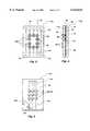
- FIG. 1comprises a top elevation of a first preferred embodiment of a chip scale package according to the present invention
- FIG. 2comprises a side sectional elevation of the package of FIG. 1, taken along line 2--2;
- FIG. 2Acomprises a schematic depicting the assembly, burn-in and testing, and singulation of packages according to the present invention fabricated on a wafer scale;
- FIG. 3comprises a top elevation of a second preferred embodiment of a chip scale package according to the present invention.
- FIG. 4comprises a partial side sectional elevation of the package of FIG. 3, taken along line 4--4;
- FIG. 5comprises a top elevation of a third preferred embodiment of a chip scale package according to the present invention.
- FIG. 6comprises a top elevation of a fourth preferred embodiment of a chip scale package according to the present invention.
- FIG. 7comprises a side sectional elevation of the package of FIG. 6, taken along line 7--7;
- FIG. 8is a schematic partial sectional illustration of the package of FIGS. 6 and 7 in a DDC arrangement
- FIG. 9is a top elevation of a fifth preferred embodiment of a chip scale package according to the invention.
- FIG. 10is a side schematic elevation of two packages according to the present invention assembled by flip-chip type attach in a face-to-face stack.
- FIGS. 1 and 2depict one preferred embodiment of a package 10 according to the present invention, including die 12 carrying an integrated circuit, as well known in the art, comprised of a plurality of active devices in combination with selected passive devices (resistors, capacitors, etc.) as desired on its face side or active surface 14.
- a dynamic random access memory circuitis exemplary of such an integrated circuit, although circuits of any type or for any function, such as processors, formed on dies may be packaged according to the invention.
- the integrated circuitelectrically communicates with an external circuit in which it is employed through a plurality of contacts, commonly termed bond pads 16, located on active surface 14.
- Package 10is fabricated by passivating the active surface 14 of die 12, as known in the art, by oxidizing or nitriding to form a silicon dioxide or silicon nitride layer 18 or a combination of the two.
- Spin on glass (SOG) or polyimidecan also be used.
- Blank 20is bonded or fused to die 12 by any one of a number of materials 24 known in the art, including, by way of example only, boron phosphorous silicate glass (BPSG), polymer adhesives such as epoxies, reflowable glass, photoresists, and polyimides.
- BPSGboron phosphorous silicate glass
- the entire exterior of the resulting laminateis then passivated, again as by nitriding or oxidizing (using techniques such as plasma-enhanced chemical vapor deposition or PECVD, for example), resulting in a passive exterior layer 26.
- PECVDplasma-enhanced chemical vapor deposition
- An exemplary wire bond 28is depicted in one aperture 22 in FIG. 1.
- solder bumping of the bond pads 16is to be effected, it is desirable to provide a solder-wettable surface on bond pads 16. This may be achieved by electroless plating of a copper layer 30 on bond pads 16 or, more preferably, for better metallization adhesion and greater solder-wettable surface area, by deposition of a Cr, Cr/Cu, Cu multi-layer or sandwich coating 32 (see FIG. 1) on bond pads 16 and walls 34 of apertures 22.
- the latter type of coatingmay be effected by sputtering, plasma-enhanced chemical vapor deposition (PECVD), or chemical vapor deposition (CVD), as known in the art, and requires subsequent removal of the coating from the surface of the package 10 while the aperture wall 34 and bond pad 16 areas are protected by a resist. Such removal may be rapidly and accurately effected by chemical mechanical polishing (CMP) techniques as known in the art.
- Solder paste 36(typically 95% Pb/5% Sn) may then be stencilled into apertures 22, and then heated to reflow, as known in the art.
- the metallized aperture walls 34being solder-wettable, as noted above, aid in defining the solder "ball" 38 protruding from the package after reflow.
- the angle of walls 34 to the horizontal formed using a preferred anisotropic wet etch such as a KOH:H 2 O mixtureis approximately 54° to the horizontal, or plane of the active surface 14, and provides improved strength during solder ball 38 formation by increasing surface area exposed to shear forces.
- electrolessly-plated bumps or contacts 42may be formed in apertures 22 as known in the art.
- a conductive structurerenders package 10 especially suitable for tab automated bonding (TAB) applications, wherein the terminal ends of a conductor-carrying, flexible, dielectric film (typically a polyimide) are gang-bonded to the contacts (pads, or in this case, bumps) of a die.
- conductive polymer bumps or pillars 44such as silver-filled epoxies, may also be deposited, as by stencilling, into apertures 22.
- a wafer-sized blank 320is appropriately micromachined (etched) with the desired pattern of apertures 22 to correspond to a large plurality of dies 12 to be found on a typical wafer 312.
- the wafer-sized blank 320is then aligned with and laminated to the wafer 312 after the latter has been passivated.
- the assembly 310 exterioris passivated, and any further bond pad/aperture wall metallization effected, after which conductive bumps or balls may be formed as described above.
- the wafer-sized assembly 310is then subjected to electrical testing and burn-in before the wafer assembly 310 is sawn to singulate the packages 10, thus providing packaged known good die (KGD) upon singulation.
- packaged die 10may be severed from the wafer assembly 310 singularly, or in groups, as desired. It is also contemplated that an entire unsevered wafer assembly 310 may be tested and burned-in and then used as fabricated as a wafer-scale package, particularly for large-capacity memory requirements.
- blank 20has been characterized as being comprised of silicon (e.g, a wafer blank), it will be recognized by those skilled in the art that the invention is not so limited. For example, certain ceramics and mullites having suitable CTE's may be employed. Further, if the die-bearing wafer is of GaAs, a wafer of like material is also obviously suitable. The significant requirement for the package blank is its susceptibility to highly accurate micromachining, mechanical properties compatible with those of the die-bearing wafer, lack of adverse electrical characteristics, and bondability to the latter using normal bonding materials and techniques.
- FIGS. 3 and 4depict another preferred embodiment 110 of the package of the invention.
- a die 12is employed as before.
- circuit traces 114have been applied by means well known in the art to the face side 14 of die 12 over passivation layer 18 to reroute the external connection locations of die 12 from bond pads 16 to new, relocated bond pads 116.
- Blank 20is then micromachined or etched with apertures 22 in locations corresponding to the locations of new bond pads 116.
- a die 12 having fine-pitch peripheral bond pads 16 or a central row of such bond pads 16 and thus being unsuitable for flip-chip bonding due to pitch limitations of solder or other conductive bumpsmay be reconfigured or retrofitted with more widely-spaced or larger-pitched bond pads 116 in an area array, for example, at the center of the die 12 as shown.
- dies carrying a variety of bond pad patternsmay be standardized in their external connection arrangements.
- a logical extension of the embodiment 110 of FIGS. 3 and 4, as shown in FIG. 5,is to reroute the circuit traces 114 of die 12 during fabrication thereof, rather than subsequent thereto as described above, so that only the new bond pads 116 are present, original bond pads 16 being eliminated.
- Such an approachmay well require formation of an extra or intermediate surface passivation layer 118 on the die face side, or dielectric coating as by a spin-on polyimide followed by formation of traces 114, but such operation is easily effectuated by equipment and technology usually already used in the fab.
- rerouting circuit traces 114 and new bond pads 116may be formed on the back side of blank 20, as by stencilling of a conductor or adherence thereto of a conductor-carrying dielectric film, and the blank 20 etched through from its face side to form apertures 22 at the new bond pad locations.
- FIGS. 6 and 7Yet another preferred embodiment 210 of the invention is depicted in FIGS. 6 and 7, wherein bond pads 16 are rerouted by circuit traces 114 to new bond pads 116 onto which apertures 22 of a blank 20 open. In this instance, however, the bond pads 16 are rerouted to new bond pads 116 adjacent the edge of package 210 for a DDC-type connect to a carrier 216, as schematically depicted in FIG. 8.
- Shallow, mutually parallel trenches 122 perpendicular to an edge of package 210may be machined (etched) in communication with apertures 22 having new bond pads 116 at the bottoms thereof.
- each trench 122may be metallized in communication with its associated new bond pad 116 as previously described with respect to preparation for solder bumping, although the preferred materials may differ since no solder-wettability is required.
- metallized trenches, rather than bond pads 116may serve as external electrical connections for package 210.
- the trenches 122may actually extend all the way from the original bond pads 16 to the package edge as shown in broken lines 122' on FIG. 6, with appropriate metallization of the trench providing a conductive path on the face side of blank 20.
- Such trencheswould extend all the way through blank 20 to communicate with bond pads 16, but then would rise to a shallower depth thereafter to place the material of the blank between the trench circuit trace and the underlying die 12.
- the apertures 22 and all but the portion of trench 122 to be electrically contactedmay be subsequently covered or filled with a protective dielectric 124 such as a polyimide or a photoresist.
- a protective dielectric 124such as a polyimide or a photoresist.
- the apertures passing through the blank of package 10may be formed as extended grooves or trenches 22' passing over a plurality of bond pads, rather than as discrete, one-per-bond pad apertures, if desired.
- conductive bumpssuch as solder balls 38 may be formed at desired locations along each groove. See FIG. 9.
- packages according to the inventionmay be employed in face-to-face die or even wafer stacking as depicted in FIG. 10, wherein solder or conductive epoxy connections 338 are made between facing packages 10 to form an assembly 300, and external connections 302 of the assembly may be in the form of metallized traces extending on the surface of, or in trenches in the surface of, the blanks 20 of one or both packages 10.
Landscapes
- Engineering & Computer Science (AREA)
- Computer Hardware Design (AREA)
- Microelectronics & Electronic Packaging (AREA)
- Power Engineering (AREA)
- Physics & Mathematics (AREA)
- Condensed Matter Physics & Semiconductors (AREA)
- General Physics & Mathematics (AREA)
- Manufacturing & Machinery (AREA)
- Wire Bonding (AREA)
- Semiconductor Integrated Circuits (AREA)
Abstract
Description
Claims (30)
Priority Applications (1)
| Application Number | Priority Date | Filing Date | Title |
|---|---|---|---|
| US09/156,300US6124634A (en) | 1996-03-07 | 1998-09-17 | Micromachined chip scale package |
Applications Claiming Priority (2)
| Application Number | Priority Date | Filing Date | Title |
|---|---|---|---|
| US08/612,059US6072236A (en) | 1996-03-07 | 1996-03-07 | Micromachined chip scale package |
| US09/156,300US6124634A (en) | 1996-03-07 | 1998-09-17 | Micromachined chip scale package |
Related Parent Applications (1)
| Application Number | Title | Priority Date | Filing Date |
|---|---|---|---|
| US08/612,059ContinuationUS6072236A (en) | 1996-03-07 | 1996-03-07 | Micromachined chip scale package |
Publications (1)
| Publication Number | Publication Date |
|---|---|
| US6124634Atrue US6124634A (en) | 2000-09-26 |
Family
ID=24451549
Family Applications (5)
| Application Number | Title | Priority Date | Filing Date |
|---|---|---|---|
| US08/612,059Expired - LifetimeUS6072236A (en) | 1996-03-07 | 1996-03-07 | Micromachined chip scale package |
| US08/811,711Expired - LifetimeUS6207548B1 (en) | 1996-03-07 | 1997-03-05 | Method for fabricating a micromachined chip scale package |
| US09/156,300Expired - LifetimeUS6124634A (en) | 1996-03-07 | 1998-09-17 | Micromachined chip scale package |
| US09/651,601Expired - Fee RelatedUS6358833B1 (en) | 1996-03-07 | 2000-08-30 | Method of fabricating a micromachined chip scale package |
| US09/769,983Expired - Fee RelatedUS6407451B2 (en) | 1996-03-07 | 2001-01-25 | Micromachined chip scale package |
Family Applications Before (2)
| Application Number | Title | Priority Date | Filing Date |
|---|---|---|---|
| US08/612,059Expired - LifetimeUS6072236A (en) | 1996-03-07 | 1996-03-07 | Micromachined chip scale package |
| US08/811,711Expired - LifetimeUS6207548B1 (en) | 1996-03-07 | 1997-03-05 | Method for fabricating a micromachined chip scale package |
Family Applications After (2)
| Application Number | Title | Priority Date | Filing Date |
|---|---|---|---|
| US09/651,601Expired - Fee RelatedUS6358833B1 (en) | 1996-03-07 | 2000-08-30 | Method of fabricating a micromachined chip scale package |
| US09/769,983Expired - Fee RelatedUS6407451B2 (en) | 1996-03-07 | 2001-01-25 | Micromachined chip scale package |
Country Status (1)
| Country | Link |
|---|---|
| US (5) | US6072236A (en) |
Cited By (102)
| Publication number | Priority date | Publication date | Assignee | Title |
|---|---|---|---|---|
| US6300670B1 (en) | 1999-07-26 | 2001-10-09 | Stmicroelectronics, Inc. | Backside bus vias |
| US6326689B1 (en)* | 1999-07-26 | 2001-12-04 | Stmicroelectronics, Inc. | Backside contact for touchchip |
| US6326677B1 (en)* | 1998-09-04 | 2001-12-04 | Cts Corporation | Ball grid array resistor network |
| US6404052B1 (en)* | 1999-07-12 | 2002-06-11 | Sony Chemicals Corp. | Multi-layer flexible printed wiring board |
| US6407451B2 (en)* | 1996-03-07 | 2002-06-18 | Micron Technology, Inc. | Micromachined chip scale package |
| US20030042581A1 (en)* | 2001-08-29 | 2003-03-06 | Fee Setho Sing | Packaged microelectronic devices and methods of forming same |
| US20030071341A1 (en)* | 2001-10-16 | 2003-04-17 | Jeung Boon Suan | Apparatus and method for leadless packaging of semiconductor devices |
| US6558600B1 (en) | 2000-05-04 | 2003-05-06 | Micron Technology, Inc. | Method for packaging microelectronic substrates |
| US6564979B2 (en) | 2001-07-18 | 2003-05-20 | Micron Technology, Inc. | Method and apparatus for dispensing adhesive on microelectronic substrate supports |
| US6576494B1 (en) | 2000-06-28 | 2003-06-10 | Micron Technology, Inc. | Recessed encapsulated microelectronic devices and methods for formation |
| US20030151132A1 (en)* | 2002-02-14 | 2003-08-14 | Crippen Warren Stuart | Microelectronic die providing improved heat dissipation, and method of packaging same |
| US20030166342A1 (en)* | 2001-05-07 | 2003-09-04 | Applied Materials, Inc. | Integrated method for release and passivation of MEMS structures |
| US6624003B1 (en) | 2002-02-06 | 2003-09-23 | Teravicta Technologies, Inc. | Integrated MEMS device and package |
| US6622380B1 (en) | 2002-02-12 | 2003-09-23 | Micron Technology, Inc. | Methods for manufacturing microelectronic devices and methods for mounting microelectronic packages to circuit boards |
| US6638595B2 (en) | 2000-06-28 | 2003-10-28 | Micron Technology, Inc. | Method and apparatus for reduced flash encapsulation of microelectronic devices |
| US6647755B2 (en) | 2001-03-07 | 2003-11-18 | Omnisonics Medical Technologies, Inc. | Method for manufacturing small diameter medical devices |
| US6653173B2 (en) | 2000-06-16 | 2003-11-25 | Micron Technology, Inc. | Method and apparatus for packaging a microelectronic die |
| US6656769B2 (en) | 2000-05-08 | 2003-12-02 | Micron Technology, Inc. | Method and apparatus for distributing mold material in a mold for packaging microelectronic devices |
| US20040026776A1 (en)* | 2002-08-08 | 2004-02-12 | Brand Joseph M. | Microelectronic devices and methods for manufacturing and operating packaged microelectronic device assemblies |
| US20040031621A1 (en)* | 2002-08-19 | 2004-02-19 | Heng Puah Kia | Packaged microelectronic component assemblies |
| US20040035917A1 (en)* | 2002-08-22 | 2004-02-26 | Michel Koopmans | Apparatus and method for depositing and reflowing solder paste on a microelectronic workpiece |
| US20040038447A1 (en)* | 2002-08-21 | 2004-02-26 | Corisis David J | Packaged microelectronic devices and methods for assembling microelectronic devices |
| US20040038449A1 (en)* | 2000-08-23 | 2004-02-26 | Corisis David J. | Stacked microelectronic dies and methods for stacking microelectronic dies |
| US20040041271A1 (en)* | 2002-08-29 | 2004-03-04 | Storli Farrah J. | Methods for wafer-level packaging of microelectronic devices and microelectronic devices formed by such methods |
| US6724090B2 (en) | 2002-04-23 | 2004-04-20 | Hynix Semiconductor Inc. | Multi-chip package and method for manufacturing the same |
| US20040100772A1 (en)* | 2002-11-22 | 2004-05-27 | Chye Lim Thiam | Packaged microelectronic component assemblies |
| US20040108937A1 (en)* | 2002-12-04 | 2004-06-10 | Craig Ernsberger | Ball grid array resistor network |
| US6750547B2 (en) | 2001-12-26 | 2004-06-15 | Micron Technology, Inc. | Multi-substrate microelectronic packages and methods for manufacture |
| US6762074B1 (en) | 2003-01-21 | 2004-07-13 | Micron Technology, Inc. | Method and apparatus for forming thin microelectronic dies |
| US20040155331A1 (en)* | 2003-02-11 | 2004-08-12 | Blaine Thurgood | Packaged microelectronic devices and methods for packaging microelectronic devices |
| US20040173899A1 (en)* | 2003-03-04 | 2004-09-09 | Peng Neo Chee | Microelectronic component assemblies employing lead frames having reduced-thickness inner lengths |
| US20040178495A1 (en)* | 2003-03-14 | 2004-09-16 | Yean Tay Wuu | Microelectronic devices and methods for packaging microelectronic devices |
| US6796028B2 (en) | 2000-08-23 | 2004-09-28 | Micron Technology, Inc. | Method of Interconnecting substrates for electrical coupling of microelectronic components |
| US20040214373A1 (en)* | 2003-04-22 | 2004-10-28 | Tongbi Jiang | Packaged microelectronic devices and methods for packaging microelectronic devices |
| US6836009B2 (en) | 2002-08-08 | 2004-12-28 | Micron Technology, Inc. | Packaged microelectronic components |
| US6838760B1 (en) | 2000-08-28 | 2005-01-04 | Micron Technology, Inc. | Packaged microelectronic devices with interconnecting units |
| US20050019988A1 (en)* | 2002-04-04 | 2005-01-27 | Tongbi Jiang | Method and apparatus for attaching microelectronic substrates and support members |
| US20050019984A1 (en)* | 2000-08-09 | 2005-01-27 | Tongbi Jiang | Multiple substrate microelectronic devices and methods of manufacture |
| US20050085006A1 (en)* | 2003-10-15 | 2005-04-21 | Voelz James L. | Methods for wafer-level packaging of microelectronic devices and microelectronic devices formed by such methods |
| US20050093174A1 (en)* | 2003-10-31 | 2005-05-05 | Seng Eric T.S. | Reduced footprint packaged microelectronic components and methods for manufacturing such microelectronic components |
| US20050104171A1 (en)* | 2003-11-13 | 2005-05-19 | Benson Peter A. | Microelectronic devices having conductive complementary structures and methods of manufacturing microelectronic devices having conductive complementary structures |
| US6921860B2 (en) | 2003-03-18 | 2005-07-26 | Micron Technology, Inc. | Microelectronic component assemblies having exposed contacts |
| US20050247039A1 (en)* | 2004-05-04 | 2005-11-10 | Textron Inc. | Disposable magnetic bedknife |
| US20050247894A1 (en)* | 2004-05-05 | 2005-11-10 | Watkins Charles M | Systems and methods for forming apertures in microfeature workpieces |
| US6979595B1 (en) | 2000-08-24 | 2005-12-27 | Micron Technology, Inc. | Packaged microelectronic devices with pressure release elements and methods for manufacturing and using such packaged microelectronic devices |
| US20060017177A1 (en)* | 2004-07-23 | 2006-01-26 | Seng Eric T S | Microelectronic component assemblies with recessed wire bonds and methods of making same |
| US20060028288A1 (en)* | 2004-08-09 | 2006-02-09 | Jason Langhorn | Ball grid array resistor capacitor network |
| US20060046346A1 (en)* | 2004-09-01 | 2006-03-02 | Benson Peter A | Methods for packaging microfeature devices and microfeature devices formed by such methods |
| US20060162850A1 (en)* | 2005-01-24 | 2006-07-27 | Micron Technology, Inc. | Methods and apparatus for releasably attaching microfeature workpieces to support members |
| US20060246621A1 (en)* | 2002-02-14 | 2006-11-02 | Intel Corporation | Microelectronic die including thermally conductive structure in a substrate thereof and method of forming same |
| US20060292858A1 (en)* | 2002-07-18 | 2006-12-28 | Micron Technology, Inc. | Techniques to create low K ILD for beol |
| US20070031998A1 (en)* | 2000-08-16 | 2007-02-08 | Micron Technology, Inc. | Method and apparatus for removing encapsulating material from a packaged microelectronic device |
| US20070036932A1 (en)* | 2005-07-19 | 2007-02-15 | Micron Technology, Inc. | Methods for releasably attaching support members to microfeature workpieces and microfeature assemblies formed using such methods |
| US20070045872A1 (en)* | 2005-08-31 | 2007-03-01 | Fee Setho S | Microelectronic devices having intermediate contacts for connection to interposer substrates, and associated methods of packaging microelectronic devices with intermediate contacts |
| US20070045865A1 (en)* | 2005-09-01 | 2007-03-01 | Tang Sanh D | Microfeature workpieces and methods of forming a redistribution layer on microfeature workpieces |
| US20070045807A1 (en)* | 2005-09-01 | 2007-03-01 | Micron Technology, Inc. | Microelectronic devices and methods for manufacturing microelectronic devices |
| US20070148820A1 (en)* | 2005-12-22 | 2007-06-28 | Micron Technology, Inc. | Microelectronic devices and methods for manufacturing microelectronic devices |
| US20070155048A1 (en)* | 2005-12-29 | 2007-07-05 | Micron Technology, Inc. | Methods for packaging microelectronic devices and microelectronic devices formed using such methods |
| US7259451B2 (en) | 2003-08-29 | 2007-08-21 | Micron Technology, Inc. | Invertible microfeature device packages |
| US20070228577A1 (en)* | 2006-03-29 | 2007-10-04 | Micron Technology, Inc. | Packaged microelectronic devices recessed in support member cavities, and associated methods |
| US20070241078A1 (en)* | 2006-03-14 | 2007-10-18 | Micron Technology, Inc. | Methods for releasably attaching support members to microfeature workpieces |
| US20080012110A1 (en)* | 2006-07-17 | 2008-01-17 | Micron Technology, Inc. | Microelectronic packages with leadframes, including leadframes configured for stacked die packages, and associated systems and methods |
| US20080048316A1 (en)* | 2006-08-25 | 2008-02-28 | Micron Technology, Inc. | Packaged microdevices and methods for manufacturing packaged microdevices |
| US20080050901A1 (en)* | 2006-08-23 | 2008-02-28 | Micron Technology, Inc. | Packaged microelectronic devices and methods for manufacturing packaged microelectronic devices |
| US20080128900A1 (en)* | 2006-12-04 | 2008-06-05 | Micron Technology, Inc. | Packaged microelectronic devices and methods for manufacturing packaged microelectronic devices |
| US7413979B2 (en) | 2003-11-13 | 2008-08-19 | Micron Technology, Inc. | Methods for forming vias in microelectronic devices, and methods for packaging microelectronic devices |
| US7425499B2 (en) | 2004-08-24 | 2008-09-16 | Micron Technology, Inc. | Methods for forming interconnects in vias and microelectronic workpieces including such interconnects |
| US20080224291A1 (en)* | 2007-03-13 | 2008-09-18 | Micron Technology, Inc. | Packaged semiconductor components having substantially rigid support members and methods of packaging semiconductor components |
| US20080224329A1 (en)* | 2007-03-13 | 2008-09-18 | Micron Technology, Inc. | Packaged microelectronic devices and methods for manufacturing packaged microelectronic devices |
| US7435913B2 (en) | 2004-08-27 | 2008-10-14 | Micron Technology, Inc. | Slanted vias for electrical circuits on circuit boards and other substrates |
| US20080315424A1 (en)* | 2001-03-30 | 2008-12-25 | Megica Corporation | Structure and manufactruing method of chip scale package |
| US20090014859A1 (en)* | 2007-07-12 | 2009-01-15 | Micron Technology, Inc. | Interconnects for packaged semiconductor devices and methods for manufacturing such devices |
| US20090026600A1 (en)* | 2007-07-24 | 2009-01-29 | Micron Technology, Inc. | Microelectronic die packages with metal leads, including metal leads for stacked die packages, and associated systems and methods |
| US20090045489A1 (en)* | 2007-08-16 | 2009-02-19 | Micron Technology, Inc. | Microelectronic die packages with leadframes, including leadframe-based interposer for stacked die packages, and associated systems and methods |
| US7494468B2 (en) | 1999-10-05 | 2009-02-24 | Omnisonics Medical Technologies, Inc. | Ultrasonic medical device operating in a transverse mode |
| US7503895B2 (en) | 1999-10-05 | 2009-03-17 | Omnisonics Medical Technologies, Inc. | Ultrasonic device for tissue ablation and sheath for use therewith |
| US7518237B2 (en) | 2005-02-08 | 2009-04-14 | Micron Technology, Inc. | Microfeature systems including adhered microfeature workpieces and support members |
| US7531453B2 (en) | 2004-06-29 | 2009-05-12 | Micron Technology, Inc. | Microelectronic devices and methods for forming interconnects in microelectronic devices |
| US20090166846A1 (en)* | 2007-12-28 | 2009-07-02 | Micron Technology, Inc. | Pass-through 3d interconnect for microelectronic dies and associated systems and methods |
| US7589008B2 (en) | 2004-12-30 | 2009-09-15 | Micron Technology, Inc. | Methods for forming interconnects in microelectronic workpieces and microelectronic workpieces formed using such methods |
| US20090267213A1 (en)* | 2001-03-05 | 2009-10-29 | Megica Corporation | Structure and manufacturing method of a chip scale package with low fabrication cost, fine pitch and high reliability solder bump |
| US20090283898A1 (en)* | 2008-05-15 | 2009-11-19 | Janzen Jeffery W | Disabling electrical connections using pass-through 3d interconnects and associated systems and methods |
| US7622377B2 (en) | 2005-09-01 | 2009-11-24 | Micron Technology, Inc. | Microfeature workpiece substrates having through-substrate vias, and associated methods of formation |
| US7629249B2 (en) | 2006-08-28 | 2009-12-08 | Micron Technology, Inc. | Microfeature workpieces having conductive interconnect structures formed by chemically reactive processes, and associated systems and methods |
| US7671459B2 (en) | 2006-02-08 | 2010-03-02 | Micron Technologies, Inc. | Microelectronic devices, stacked microelectronic devices, and methods for manufacturing such devices |
| US7683458B2 (en) | 2004-09-02 | 2010-03-23 | Micron Technology, Inc. | Through-wafer interconnects for photoimager and memory wafers |
| US7749899B2 (en) | 2006-06-01 | 2010-07-06 | Micron Technology, Inc. | Microelectronic workpieces and methods and systems for forming interconnects in microelectronic workpieces |
| US7795134B2 (en) | 2005-06-28 | 2010-09-14 | Micron Technology, Inc. | Conductive interconnect structures and formation methods using supercritical fluids |
| US7794414B2 (en) | 2004-02-09 | 2010-09-14 | Emigrant Bank, N.A. | Apparatus and method for an ultrasonic medical device operating in torsional and transverse modes |
| US20100232220A1 (en)* | 2009-03-10 | 2010-09-16 | Micron Technology, Inc. | Electronic devices formed of two or more substrates bonded together, electronic systems comprising electronic devices and methods of making electronic devices |
| US7807505B2 (en) | 2005-08-30 | 2010-10-05 | Micron Technology, Inc. | Methods for wafer-level packaging of microfeature devices and microfeature devices formed using such methods |
| US7830018B2 (en) | 2007-08-31 | 2010-11-09 | Micron Technology, Inc. | Partitioned through-layer via and associated systems and methods |
| US7833456B2 (en) | 2007-02-23 | 2010-11-16 | Micron Technology, Inc. | Systems and methods for compressing an encapsulant adjacent a semiconductor workpiece |
| US20100319855A1 (en)* | 2008-02-04 | 2010-12-23 | Eugene Technology Co., Ltd. | Substrate supporting unit, substrate processing apparatus, and method of manufacturing substrate supporting unit |
| US7863187B2 (en) | 2005-09-01 | 2011-01-04 | Micron Technology, Inc. | Microfeature workpieces and methods for forming interconnects in microfeature workpieces |
| US7884015B2 (en) | 2007-12-06 | 2011-02-08 | Micron Technology, Inc. | Methods for forming interconnects in microelectronic workpieces and microelectronic workpieces formed using such methods |
| US7902643B2 (en) | 2006-08-31 | 2011-03-08 | Micron Technology, Inc. | Microfeature workpieces having interconnects and conductive backplanes, and associated systems and methods |
| US7910385B2 (en) | 2006-05-12 | 2011-03-22 | Micron Technology, Inc. | Method of fabricating microelectronic devices |
| US7915736B2 (en) | 2005-09-01 | 2011-03-29 | Micron Technology, Inc. | Microfeature workpieces and methods for forming interconnects in microfeature workpieces |
| US8084866B2 (en) | 2003-12-10 | 2011-12-27 | Micron Technology, Inc. | Microelectronic devices and methods for filling vias in microelectronic devices |
| US8790359B2 (en) | 1999-10-05 | 2014-07-29 | Cybersonics, Inc. | Medical systems and related methods |
| US9048410B2 (en) | 2013-05-31 | 2015-06-02 | Micron Technology, Inc. | Memory devices comprising magnetic tracks individually comprising a plurality of magnetic domains having domain walls and methods of forming a memory device comprising magnetic tracks individually comprising a plurality of magnetic domains having domain walls |
Families Citing this family (105)
| Publication number | Priority date | Publication date | Assignee | Title |
|---|---|---|---|---|
| US6969635B2 (en) | 2000-12-07 | 2005-11-29 | Reflectivity, Inc. | Methods for depositing, releasing and packaging micro-electromechanical devices on wafer substrates |
| US6558979B2 (en)* | 1996-05-21 | 2003-05-06 | Micron Technology, Inc. | Use of palladium in IC manufacturing with conductive polymer bump |
| US6441487B2 (en)* | 1997-10-20 | 2002-08-27 | Flip Chip Technologies, L.L.C. | Chip scale package using large ductile solder balls |
| US6803656B2 (en)* | 1997-12-31 | 2004-10-12 | Micron Technology, Inc. | Semiconductor device including combed bond pad opening |
| US6117708A (en) | 1998-02-05 | 2000-09-12 | Micron Technology, Inc. | Use of residual organic compounds to facilitate gate break on a carrier substrate for a semiconductor device |
| IL123207A0 (en) | 1998-02-06 | 1998-09-24 | Shellcase Ltd | Integrated circuit device |
| US6624505B2 (en)* | 1998-02-06 | 2003-09-23 | Shellcase, Ltd. | Packaged integrated circuits and methods of producing thereof |
| US6331735B1 (en)* | 1998-09-25 | 2001-12-18 | Advanced Micro Devices, Inc. | Method to improve chip scale package electrostatic discharge performance and suppress marking artifacts |
| US6376352B1 (en)* | 1998-11-05 | 2002-04-23 | Texas Instruments Incorporated | Stud-cone bump for probe tips used in known good die carriers |
| EP1061578A4 (en)* | 1998-12-16 | 2001-07-18 | Seiko Epson Corp | SEMICONDUCTOR CHIP, SEMICONDUCTOR ARRANGEMENT, CIRCUIT BOARD AND ELECTRONIC DEVICE AND METHOD FOR THE PRODUCTION THEREOF |
| JP4234244B2 (en)* | 1998-12-28 | 2009-03-04 | 富士通マイクロエレクトロニクス株式会社 | Wafer level package and semiconductor device manufacturing method using wafer level package |
| US6365976B1 (en)* | 1999-02-25 | 2002-04-02 | Texas Instruments Incorporated | Integrated circuit device with depressions for receiving solder balls and method of fabrication |
| US6341418B1 (en) | 1999-04-29 | 2002-01-29 | International Business Machines Corporation | Method for direct chip attach by solder bumps and an underfill layer |
| US6228687B1 (en)* | 1999-06-28 | 2001-05-08 | Micron Technology, Inc. | Wafer-level package and methods of fabricating |
| US6562545B1 (en)* | 1999-09-17 | 2003-05-13 | Micron Technology, Inc. | Method of making a socket assembly for use with a solder ball |
| US6710454B1 (en)* | 2000-02-16 | 2004-03-23 | Micron Technology, Inc. | Adhesive layer for an electronic apparatus having multiple semiconductor devices |
| JP4403631B2 (en)* | 2000-04-24 | 2010-01-27 | ソニー株式会社 | Manufacturing method of chip-shaped electronic component and manufacturing method of pseudo wafer used for manufacturing the same |
| JP2001313350A (en)* | 2000-04-28 | 2001-11-09 | Sony Corp | Chip-shaped electronic component and its manufacturing method, and pseudo-wafer used for manufacture of chip- shaped electronic component and its manufacturing method |
| DE10029269B4 (en)* | 2000-06-14 | 2005-10-13 | Infineon Technologies Ag | Method for producing an electronic component from housing-forming substrates |
| US6552910B1 (en) | 2000-06-28 | 2003-04-22 | Micron Technology, Inc. | Stacked-die assemblies with a plurality of microelectronic devices and methods of manufacture |
| US6560117B2 (en) | 2000-06-28 | 2003-05-06 | Micron Technology, Inc. | Packaged microelectronic die assemblies and methods of manufacture |
| US6562657B1 (en)* | 2000-08-22 | 2003-05-13 | Charles W. C. Lin | Semiconductor chip assembly with simultaneously electrolessly plated contact terminal and connection joint |
| US6638831B1 (en) | 2000-08-31 | 2003-10-28 | Micron Technology, Inc. | Use of a reference fiducial on a semiconductor package to monitor and control a singulation method |
| SG112799A1 (en) | 2000-10-09 | 2005-07-28 | St Assembly Test Services Ltd | Leaded semiconductor packages and method of trimming and singulating such packages |
| JP4447143B2 (en)* | 2000-10-11 | 2010-04-07 | 新光電気工業株式会社 | Semiconductor device and manufacturing method thereof |
| US6686258B2 (en) | 2000-11-02 | 2004-02-03 | St Assembly Test Services Ltd. | Method of trimming and singulating leaded semiconductor packages |
| US6833620B1 (en)* | 2000-11-28 | 2004-12-21 | Ati Technologies, Inc. | Apparatus having reduced input output area and method thereof |
| US6995034B2 (en)* | 2000-12-07 | 2006-02-07 | Reflectivity, Inc | Methods for depositing, releasing and packaging micro-electromechanical devices on wafer substrates |
| US7307775B2 (en)* | 2000-12-07 | 2007-12-11 | Texas Instruments Incorporated | Methods for depositing, releasing and packaging micro-electromechanical devices on wafer substrates |
| KR100855015B1 (en)* | 2000-12-21 | 2008-08-28 | 테쎄라 테크놀로지스 헝가리 케이에프티. | Packaged integrated circuit and manufacturing method thereof |
| ES2292720T3 (en)* | 2001-03-09 | 2008-03-16 | Datec Coating Corporation | RESISTIVE COATING AND DRIVER DERIVED FROM SOL-GEL. |
| TW595283B (en)* | 2001-04-25 | 2004-06-21 | Benq Corp | Flexible circuit board and its manufacturing method |
| US6732913B2 (en)* | 2001-04-26 | 2004-05-11 | Advanpack Solutions Pte Ltd. | Method for forming a wafer level chip scale package, and package formed thereby |
| US6593649B1 (en)* | 2001-05-17 | 2003-07-15 | Megic Corporation | Methods of IC rerouting option for multiple package system applications |
| US6856007B2 (en) | 2001-08-28 | 2005-02-15 | Tessera, Inc. | High-frequency chip packages |
| US20030042615A1 (en) | 2001-08-30 | 2003-03-06 | Tongbi Jiang | Stacked microelectronic devices and methods of fabricating same |
| US6548376B2 (en) | 2001-08-30 | 2003-04-15 | Micron Technology, Inc. | Methods of thinning microelectronic workpieces |
| SG102639A1 (en)* | 2001-10-08 | 2004-03-26 | Micron Technology Inc | Apparatus and method for packing circuits |
| US6674174B2 (en)* | 2001-11-13 | 2004-01-06 | Skyworks Solutions, Inc. | Controlled impedance transmission lines in a redistribution layer |
| US6896760B1 (en)* | 2002-01-16 | 2005-05-24 | Micron Technology, Inc. | Fabrication of stacked microelectronic devices |
| US7198693B1 (en) | 2002-02-20 | 2007-04-03 | Micron Technology, Inc. | Microelectronic device having a plurality of stacked dies and methods for manufacturing such microelectronic assemblies |
| JP2003258154A (en)* | 2002-03-05 | 2003-09-12 | Fujitsu Ltd | Semiconductor element mounting structure |
| US7423336B2 (en)* | 2002-04-08 | 2008-09-09 | Micron Technology, Inc. | Bond pad rerouting element, rerouted semiconductor devices including the rerouting element, and assemblies including the rerouted semiconductor devices |
| US7579681B2 (en)* | 2002-06-11 | 2009-08-25 | Micron Technology, Inc. | Super high density module with integrated wafer level packages |
| KR100481216B1 (en)* | 2002-06-07 | 2005-04-08 | 엘지전자 주식회사 | Ball Grid Array Package And Method Of Fabricating The Same |
| SG142115A1 (en)* | 2002-06-14 | 2008-05-28 | Micron Technology Inc | Wafer level packaging |
| SG111069A1 (en)* | 2002-06-18 | 2005-05-30 | Micron Technology Inc | Semiconductor devices including peripherally located bond pads, assemblies, packages, and methods |
| SG107595A1 (en) | 2002-06-18 | 2004-12-29 | Micron Technology Inc | Semiconductor devices and semiconductor device components with peripherally located, castellated contacts, assembles and packages including such semiconductor devices or packages and associated methods |
| US7033664B2 (en) | 2002-10-22 | 2006-04-25 | Tessera Technologies Hungary Kft | Methods for producing packaged integrated circuit devices and packaged integrated circuit devices produced thereby |
| JP3625815B2 (en)* | 2002-11-12 | 2005-03-02 | 沖電気工業株式会社 | Semiconductor device and manufacturing method thereof |
| KR100447851B1 (en)* | 2002-11-14 | 2004-09-08 | 삼성전자주식회사 | Wafer level Bonding method of flip-chip manner for semiconductor apparatus in lateral bonded type |
| US7405860B2 (en)* | 2002-11-26 | 2008-07-29 | Texas Instruments Incorporated | Spatial light modulators with light blocking/absorbing areas |
| US6774482B2 (en)* | 2002-12-27 | 2004-08-10 | International Business Machines Corporation | Chip cooling |
| KR100512971B1 (en)* | 2003-02-24 | 2005-09-07 | 삼성전자주식회사 | Manufacturing method of micro electro mechanical system using solder ball |
| US6917090B2 (en)* | 2003-04-07 | 2005-07-12 | Micron Technology, Inc. | Chip scale image sensor package |
| SG119185A1 (en) | 2003-05-06 | 2006-02-28 | Micron Technology Inc | Method for packaging circuits and packaged circuits |
| US20040232535A1 (en)* | 2003-05-22 | 2004-11-25 | Terry Tarn | Microelectromechanical device packages with integral heaters |
| US6972480B2 (en) | 2003-06-16 | 2005-12-06 | Shellcase Ltd. | Methods and apparatus for packaging integrated circuit devices |
| CN100587962C (en) | 2003-07-03 | 2010-02-03 | 泰塞拉技术匈牙利公司 | Method and apparatus for packaging integrated circuit devices |
| US7071421B2 (en) | 2003-08-29 | 2006-07-04 | Micron Technology, Inc. | Stacked microfeature devices and associated methods |
| US7345350B2 (en) | 2003-09-23 | 2008-03-18 | Micron Technology, Inc. | Process and integration scheme for fabricating conductive components, through-vias and semiconductor components including conductive through-wafer vias |
| WO2005031861A1 (en) | 2003-09-26 | 2005-04-07 | Tessera, Inc. | Structure and method of making capped chips including a flowable conductive medium |
| SG120123A1 (en)* | 2003-09-30 | 2006-03-28 | Micron Technology Inc | Castellated chip-scale packages and methods for fabricating the same |
| US20050093134A1 (en)* | 2003-10-30 | 2005-05-05 | Terry Tarn | Device packages with low stress assembly process |
| US7316063B2 (en)* | 2004-01-12 | 2008-01-08 | Micron Technology, Inc. | Methods of fabricating substrates including at least one conductive via |
| US7602618B2 (en)* | 2004-08-25 | 2009-10-13 | Micron Technology, Inc. | Methods and apparatuses for transferring heat from stacked microfeature devices |
| US7217995B2 (en)* | 2004-11-12 | 2007-05-15 | Macronix International Co., Ltd. | Apparatus for stacking electrical components using insulated and interconnecting via |
| DE102004056534A1 (en)* | 2004-11-23 | 2006-06-01 | Infineon Technologies Ag | Semiconductor component with a semiconductor chip and with external contacts and method for producing the same |
| US8143095B2 (en) | 2005-03-22 | 2012-03-27 | Tessera, Inc. | Sequential fabrication of vertical conductive interconnects in capped chips |
| US7508063B2 (en)* | 2005-04-05 | 2009-03-24 | Texas Instruments Incorporated | Low cost hermetically sealed package |
| US7408250B2 (en)* | 2005-04-05 | 2008-08-05 | Texas Instruments Incorporated | Micromirror array device with compliant adhesive |
| JP4577688B2 (en) | 2005-05-09 | 2010-11-10 | エルピーダメモリ株式会社 | Semiconductor chip selection method, semiconductor chip, and semiconductor integrated circuit device |
| US20060261498A1 (en)* | 2005-05-17 | 2006-11-23 | Micron Technology, Inc. | Methods and apparatuses for encapsulating microelectronic devices |
| DE102005037321B4 (en)* | 2005-08-04 | 2013-08-01 | Infineon Technologies Ag | Process for the production of semiconductor components with interconnects between semiconductor chips and a circuit carrier |
| US7566853B2 (en)* | 2005-08-12 | 2009-07-28 | Tessera, Inc. | Image sensor employing a plurality of photodetector arrays and/or rear-illuminated architecture |
| SG130055A1 (en)* | 2005-08-19 | 2007-03-20 | Micron Technology Inc | Microelectronic devices, stacked microelectronic devices, and methods for manufacturing microelectronic devices |
| SG130061A1 (en)* | 2005-08-24 | 2007-03-20 | Micron Technology Inc | Microelectronic devices and microelectronic support devices, and associated assemblies and methods |
| SG130066A1 (en)* | 2005-08-26 | 2007-03-20 | Micron Technology Inc | Microelectronic device packages, stacked microelectronic device packages, and methods for manufacturing microelectronic devices |
| US7485969B2 (en)* | 2005-09-01 | 2009-02-03 | Micron Technology, Inc. | Stacked microelectronic devices and methods for manufacturing microelectronic devices |
| US7619312B2 (en)* | 2005-10-03 | 2009-11-17 | Sun Microsystems, Inc. | Method and apparatus for precisely aligning integrated circuit chips |
| US7936062B2 (en) | 2006-01-23 | 2011-05-03 | Tessera Technologies Ireland Limited | Wafer level chip packaging |
| KR100699807B1 (en)* | 2006-01-26 | 2007-03-28 | 삼성전자주식회사 | Stacked chip and having stacked chip package |
| SG135979A1 (en)* | 2006-03-08 | 2007-10-29 | Micron Technology Inc | Microelectronic device assemblies including assemblies with recurved leadframes, and associated methods |
| US7990727B1 (en)* | 2006-04-03 | 2011-08-02 | Aprolase Development Co., Llc | Ball grid array stack |
| US8604605B2 (en) | 2007-01-05 | 2013-12-10 | Invensas Corp. | Microelectronic assembly with multi-layer support structure |
| JP5425404B2 (en)* | 2008-01-18 | 2014-02-26 | 東京エレクトロン株式会社 | Method for processing amorphous carbon film and method for manufacturing semiconductor device using the same |
| US7872332B2 (en) | 2008-09-11 | 2011-01-18 | Micron Technology, Inc. | Interconnect structures for stacked dies, including penetrating structures for through-silicon vias, and associated systems and methods |
| US8472199B2 (en) | 2008-11-13 | 2013-06-25 | Mosaid Technologies Incorporated | System including a plurality of encapsulated semiconductor chips |
| US8093700B2 (en)* | 2008-12-16 | 2012-01-10 | Freescale Semiconductor, Inc. | Packaging millimeter wave modules |
| US8637983B2 (en)* | 2008-12-19 | 2014-01-28 | Ati Technologies Ulc | Face-to-face (F2F) hybrid structure for an integrated circuit |
| US8198131B2 (en)* | 2009-11-18 | 2012-06-12 | Advanced Semiconductor Engineering, Inc. | Stackable semiconductor device packages |
| TWI408785B (en)* | 2009-12-31 | 2013-09-11 | Advanced Semiconductor Eng | Semiconductor package |
| US8569894B2 (en) | 2010-01-13 | 2013-10-29 | Advanced Semiconductor Engineering, Inc. | Semiconductor package with single sided substrate design and manufacturing methods thereof |
| TWI419283B (en) | 2010-02-10 | 2013-12-11 | Advanced Semiconductor Eng | Package structure |
| TWI411075B (en) | 2010-03-22 | 2013-10-01 | Advanced Semiconductor Eng | Semiconductor package and manufacturing method thereof |
| US8624374B2 (en) | 2010-04-02 | 2014-01-07 | Advanced Semiconductor Engineering, Inc. | Semiconductor device packages with fan-out and with connecting elements for stacking and manufacturing methods thereof |
| US8278746B2 (en) | 2010-04-02 | 2012-10-02 | Advanced Semiconductor Engineering, Inc. | Semiconductor device packages including connecting elements |
| US9188751B2 (en) | 2010-08-31 | 2015-11-17 | Avago Technologies General Ip (Singapore) Pte. Ltd. | Flip-chip assembly comprising an array of vertical cavity surface emitting lasers (VCSELSs), and an optical transmitter assembly that incorporates the flip-chip assembly |
| US9620934B2 (en)* | 2010-08-31 | 2017-04-11 | Avago Technologies General Ip (Singapore) Pte. Ltd. | Flip-chip assembly comprising an array of vertical cavity surface emitting lasers (VCSELs) |
| TWI451546B (en) | 2010-10-29 | 2014-09-01 | Advanced Semiconductor Eng | Stacked semiconductor package, semiconductor package thereof and method for making a semiconductor package |
| US9171792B2 (en) | 2011-02-28 | 2015-10-27 | Advanced Semiconductor Engineering, Inc. | Semiconductor device packages having a side-by-side device arrangement and stacking functionality |
| US8659153B2 (en) | 2012-07-16 | 2014-02-25 | Micron Technology, Inc. | Pillar on pad interconnect structures, semiconductor dice and die assemblies including such interconnect structures, and related methods |
| US8963343B1 (en)* | 2013-09-27 | 2015-02-24 | Cypress Semiconductor Corporation | Ferroelectric memories with a stress buffer |
| KR102468796B1 (en) | 2015-08-28 | 2022-11-18 | 삼성전자주식회사 | Printed circuit board and semiconductor package including the same |
| CN115332120B (en)* | 2022-08-18 | 2023-10-03 | 无锡市华宇光微电子科技有限公司 | Automatic chip detection packaging device |
Citations (20)
| Publication number | Priority date | Publication date | Assignee | Title |
|---|---|---|---|---|
| US4542397A (en)* | 1984-04-12 | 1985-09-17 | Xerox Corporation | Self aligning small scale integrated circuit semiconductor chips to form large area arrays |
| JPH0348435A (en)* | 1989-07-17 | 1991-03-01 | Oki Electric Ind Co Ltd | Mounting structure of flip chip element |
| US5018002A (en)* | 1989-07-03 | 1991-05-21 | General Electric Company | High current hermetic package including an internal foil and having a lead extending through the package lid and a packaged semiconductor chip |
| US5136364A (en)* | 1991-06-12 | 1992-08-04 | National Semiconductor Corporation | Semiconductor die sealing |
| US5248797A (en)* | 1992-08-13 | 1993-09-28 | American Cyanamid Company | Method for the production of 9-amino-6-demethyl-6-deoxytetracycline |
| US5248903A (en)* | 1992-09-18 | 1993-09-28 | Lsi Logic Corporation | Composite bond pads for semiconductor devices |
| US5258648A (en)* | 1991-06-27 | 1993-11-02 | Motorola, Inc. | Composite flip chip semiconductor device with an interposer having test contacts formed along its periphery |
| US5262927A (en)* | 1992-02-07 | 1993-11-16 | Lsi Logic Corporation | Partially-molded, PCB chip carrier package |
| JPH0637157A (en)* | 1992-07-16 | 1994-02-10 | Kawasaki Steel Corp | Semiconductor wafer and inspecting method therefor |
| US5291064A (en)* | 1991-04-16 | 1994-03-01 | Nec Corporation | Package structure for semiconductor device having a flexible wiring circuit member spaced from the package casing |
| US5424652A (en)* | 1992-06-10 | 1995-06-13 | Micron Technology, Inc. | Method and apparatus for testing an unpackaged semiconductor die |
| US5441917A (en)* | 1992-07-17 | 1995-08-15 | Lsi Logic Corporation | Method of laying out bond pads on a semiconductor die |
| US5468681A (en)* | 1989-08-28 | 1995-11-21 | Lsi Logic Corporation | Process for interconnecting conductive substrates using an interposer having conductive plastic filled vias |
| US5481135A (en)* | 1992-08-31 | 1996-01-02 | Dow Corning Corporation | Hermetic protection for integrated circuits |
| US5508230A (en)* | 1993-07-29 | 1996-04-16 | Motorola, Inc. | Method for making a semiconductor device with diamond heat dissipation layer |
| US5553769A (en)* | 1992-11-12 | 1996-09-10 | International Business Machine Corporation | Interconnection of a carrier substrate and a semiconductor device |
| US5579573A (en)* | 1994-10-11 | 1996-12-03 | Ford Motor Company | Method for fabricating an undercoated chip electrically interconnected to a substrate |
| US5629241A (en)* | 1995-07-07 | 1997-05-13 | Hughes Aircraft Company | Microwave/millimeter wave circuit structure with discrete flip-chip mounted elements, and method of fabricating the same |
| US5814889A (en)* | 1995-06-05 | 1998-09-29 | Harris Corporation | Intergrated circuit with coaxial isolation and method |
| US5856705A (en)* | 1993-01-25 | 1999-01-05 | Intel Corporation | Sealed semiconductor chip and process for fabricating sealed semiconductor chip |
Family Cites Families (5)
| Publication number | Priority date | Publication date | Assignee | Title |
|---|---|---|---|---|
| DE3143776A1 (en) | 1981-11-04 | 1983-05-11 | Patent-Treuhand-Gesellschaft für elektrische Glühlampen mbH, 8000 München | "LIGHTING DEVICE FOR PROJECTION DEVICES" |
| JPH05152452A (en) | 1991-11-27 | 1993-06-18 | Oki Electric Ind Co Ltd | Method of forming air bridge wiring |
| US5989936A (en)* | 1994-07-07 | 1999-11-23 | Tessera, Inc. | Microelectronic assembly fabrication with terminal formation from a conductive layer |
| KR0182073B1 (en)* | 1995-12-22 | 1999-03-20 | 황인길 | Semiconductor chip scale semiconductor package and manufacturing method thereof |
| US6072236A (en)* | 1996-03-07 | 2000-06-06 | Micron Technology, Inc. | Micromachined chip scale package |
- 1996
- 1996-03-07USUS08/612,059patent/US6072236A/ennot_activeExpired - Lifetime
- 1997
- 1997-03-05USUS08/811,711patent/US6207548B1/ennot_activeExpired - Lifetime
- 1998
- 1998-09-17USUS09/156,300patent/US6124634A/ennot_activeExpired - Lifetime
- 2000
- 2000-08-30USUS09/651,601patent/US6358833B1/ennot_activeExpired - Fee Related
- 2001
- 2001-01-25USUS09/769,983patent/US6407451B2/ennot_activeExpired - Fee Related
Patent Citations (21)
| Publication number | Priority date | Publication date | Assignee | Title |
|---|---|---|---|---|
| US4542397A (en)* | 1984-04-12 | 1985-09-17 | Xerox Corporation | Self aligning small scale integrated circuit semiconductor chips to form large area arrays |
| US5018002A (en)* | 1989-07-03 | 1991-05-21 | General Electric Company | High current hermetic package including an internal foil and having a lead extending through the package lid and a packaged semiconductor chip |
| JPH0348435A (en)* | 1989-07-17 | 1991-03-01 | Oki Electric Ind Co Ltd | Mounting structure of flip chip element |
| US5821624A (en)* | 1989-08-28 | 1998-10-13 | Lsi Logic Corporation | Semiconductor device assembly techniques using preformed planar structures |
| US5468681A (en)* | 1989-08-28 | 1995-11-21 | Lsi Logic Corporation | Process for interconnecting conductive substrates using an interposer having conductive plastic filled vias |
| US5291064A (en)* | 1991-04-16 | 1994-03-01 | Nec Corporation | Package structure for semiconductor device having a flexible wiring circuit member spaced from the package casing |
| US5136364A (en)* | 1991-06-12 | 1992-08-04 | National Semiconductor Corporation | Semiconductor die sealing |
| US5258648A (en)* | 1991-06-27 | 1993-11-02 | Motorola, Inc. | Composite flip chip semiconductor device with an interposer having test contacts formed along its periphery |
| US5262927A (en)* | 1992-02-07 | 1993-11-16 | Lsi Logic Corporation | Partially-molded, PCB chip carrier package |
| US5424652A (en)* | 1992-06-10 | 1995-06-13 | Micron Technology, Inc. | Method and apparatus for testing an unpackaged semiconductor die |
| JPH0637157A (en)* | 1992-07-16 | 1994-02-10 | Kawasaki Steel Corp | Semiconductor wafer and inspecting method therefor |
| US5441917A (en)* | 1992-07-17 | 1995-08-15 | Lsi Logic Corporation | Method of laying out bond pads on a semiconductor die |
| US5248797A (en)* | 1992-08-13 | 1993-09-28 | American Cyanamid Company | Method for the production of 9-amino-6-demethyl-6-deoxytetracycline |
| US5481135A (en)* | 1992-08-31 | 1996-01-02 | Dow Corning Corporation | Hermetic protection for integrated circuits |
| US5248903A (en)* | 1992-09-18 | 1993-09-28 | Lsi Logic Corporation | Composite bond pads for semiconductor devices |
| US5553769A (en)* | 1992-11-12 | 1996-09-10 | International Business Machine Corporation | Interconnection of a carrier substrate and a semiconductor device |
| US5856705A (en)* | 1993-01-25 | 1999-01-05 | Intel Corporation | Sealed semiconductor chip and process for fabricating sealed semiconductor chip |
| US5508230A (en)* | 1993-07-29 | 1996-04-16 | Motorola, Inc. | Method for making a semiconductor device with diamond heat dissipation layer |
| US5579573A (en)* | 1994-10-11 | 1996-12-03 | Ford Motor Company | Method for fabricating an undercoated chip electrically interconnected to a substrate |
| US5814889A (en)* | 1995-06-05 | 1998-09-29 | Harris Corporation | Intergrated circuit with coaxial isolation and method |
| US5629241A (en)* | 1995-07-07 | 1997-05-13 | Hughes Aircraft Company | Microwave/millimeter wave circuit structure with discrete flip-chip mounted elements, and method of fabricating the same |
Cited By (327)
| Publication number | Priority date | Publication date | Assignee | Title |
|---|---|---|---|---|
| US6407451B2 (en)* | 1996-03-07 | 2002-06-18 | Micron Technology, Inc. | Micromachined chip scale package |
| US6326677B1 (en)* | 1998-09-04 | 2001-12-04 | Cts Corporation | Ball grid array resistor network |
| US6404052B1 (en)* | 1999-07-12 | 2002-06-11 | Sony Chemicals Corp. | Multi-layer flexible printed wiring board |
| US6746953B2 (en) | 1999-07-26 | 2004-06-08 | Stmicroelectronics, Inc. | Method of forming backside bus vias |
| US6326689B1 (en)* | 1999-07-26 | 2001-12-04 | Stmicroelectronics, Inc. | Backside contact for touchchip |
| US7339204B2 (en) | 1999-07-26 | 2008-03-04 | Stmicroelectronics, Inc. | Backside contact for touchchip |
| US6300670B1 (en) | 1999-07-26 | 2001-10-09 | Stmicroelectronics, Inc. | Backside bus vias |
| US7503895B2 (en) | 1999-10-05 | 2009-03-17 | Omnisonics Medical Technologies, Inc. | Ultrasonic device for tissue ablation and sheath for use therewith |
| US7494468B2 (en) | 1999-10-05 | 2009-02-24 | Omnisonics Medical Technologies, Inc. | Ultrasonic medical device operating in a transverse mode |
| US8790359B2 (en) | 1999-10-05 | 2014-07-29 | Cybersonics, Inc. | Medical systems and related methods |
| US20030209831A1 (en)* | 2000-05-04 | 2003-11-13 | Williams Vernon M. | Method and apparatus for packaging microelectronic substrates |
| US6558600B1 (en) | 2000-05-04 | 2003-05-06 | Micron Technology, Inc. | Method for packaging microelectronic substrates |
| US6656769B2 (en) | 2000-05-08 | 2003-12-02 | Micron Technology, Inc. | Method and apparatus for distributing mold material in a mold for packaging microelectronic devices |
| US6653173B2 (en) | 2000-06-16 | 2003-11-25 | Micron Technology, Inc. | Method and apparatus for packaging a microelectronic die |
| US6664139B2 (en) | 2000-06-16 | 2003-12-16 | Micron Technology, Inc. | Method and apparatus for packaging a microelectronic die |
| US6683388B2 (en) | 2000-06-16 | 2004-01-27 | Micron Technology, Inc. | Method and apparatus for packaging a microelectronic die |
| US6677675B2 (en) | 2000-06-16 | 2004-01-13 | Micron Technology, Inc. | Microelectronic devices and microelectronic die packages |
| US6819003B2 (en) | 2000-06-28 | 2004-11-16 | Micron Technology Inc. | Recessed encapsulated microelectronic devices and methods for formation |
| US6576494B1 (en) | 2000-06-28 | 2003-06-10 | Micron Technology, Inc. | Recessed encapsulated microelectronic devices and methods for formation |
| US6644949B2 (en) | 2000-06-28 | 2003-11-11 | Micron Technology, Inc. | Apparatus for reduced flash encapsulation of microelectronic devices |
| US6638595B2 (en) | 2000-06-28 | 2003-10-28 | Micron Technology, Inc. | Method and apparatus for reduced flash encapsulation of microelectronic devices |
| US6841423B2 (en) | 2000-06-28 | 2005-01-11 | Micron Technology, Inc. | Methods for formation of recessed encapsulated microelectronic devices |
| US7298031B1 (en)* | 2000-08-09 | 2007-11-20 | Micron Technology, Inc. | Multiple substrate microelectronic devices and methods of manufacture |
| US20050019984A1 (en)* | 2000-08-09 | 2005-01-27 | Tongbi Jiang | Multiple substrate microelectronic devices and methods of manufacture |
| US7253025B2 (en) | 2000-08-09 | 2007-08-07 | Micron Technology, Inc. | Multiple substrate microelectronic devices and methods of manufacture |
| US7405487B2 (en) | 2000-08-16 | 2008-07-29 | Micron Technology, Inc. | Method and apparatus for removing encapsulating material from a packaged microelectronic device |
| US7273769B1 (en) | 2000-08-16 | 2007-09-25 | Micron Technology, Inc. | Method and apparatus for removing encapsulating material from a packaged microelectronic device |
| US20070031998A1 (en)* | 2000-08-16 | 2007-02-08 | Micron Technology, Inc. | Method and apparatus for removing encapsulating material from a packaged microelectronic device |
| US7235871B2 (en) | 2000-08-23 | 2007-06-26 | Micron Technology, Inc. | Stacked microelectronic dies |
| US20040038449A1 (en)* | 2000-08-23 | 2004-02-26 | Corisis David J. | Stacked microelectronic dies and methods for stacking microelectronic dies |
| US8587109B2 (en) | 2000-08-23 | 2013-11-19 | Micron Technology, Inc. | Stacked microelectronic dies and methods for stacking microelectronic dies |
| US6796028B2 (en) | 2000-08-23 | 2004-09-28 | Micron Technology, Inc. | Method of Interconnecting substrates for electrical coupling of microelectronic components |
| US6982386B2 (en) | 2000-08-23 | 2006-01-03 | Micron Technology, Inc. | Interconnecting substrates for electrical coupling of microelectronic components |
| US20070210435A1 (en)* | 2000-08-23 | 2007-09-13 | Micron Technology, Inc. | Stacked microelectronic dies and methods for stacking microelectronic dies |
| US6983551B2 (en) | 2000-08-23 | 2006-01-10 | Micron Technology, Inc. | Interconnecting substrates for electrical coupling of microelectronic components |
| US8067827B2 (en) | 2000-08-23 | 2011-11-29 | Micron Technology, Inc. | Stacked microelectronic device assemblies |
| US6979595B1 (en) | 2000-08-24 | 2005-12-27 | Micron Technology, Inc. | Packaged microelectronic devices with pressure release elements and methods for manufacturing and using such packaged microelectronic devices |
| US7049685B2 (en) | 2000-08-24 | 2006-05-23 | Micron Technology, Inc. | Packaged microelectronic devices with pressure release elements and methods for manufacturing and using such packaged microelectronic devices |
| US6838760B1 (en) | 2000-08-28 | 2005-01-04 | Micron Technology, Inc. | Packaged microelectronic devices with interconnecting units |
| US7101737B2 (en) | 2000-08-28 | 2006-09-05 | Micron Technology, Inc. | Method of encapsulating interconnecting units in packaged microelectronic devices |
| US7332376B2 (en) | 2000-08-28 | 2008-02-19 | Micron Technology, Inc. | Method of encapsulating packaged microelectronic devices with a barrier |
| US8158508B2 (en) | 2001-03-05 | 2012-04-17 | Megica Corporation | Structure and manufacturing method of a chip scale package |
| US20090267213A1 (en)* | 2001-03-05 | 2009-10-29 | Megica Corporation | Structure and manufacturing method of a chip scale package with low fabrication cost, fine pitch and high reliability solder bump |
| US7902679B2 (en) | 2001-03-05 | 2011-03-08 | Megica Corporation | Structure and manufacturing method of a chip scale package with low fabrication cost, fine pitch and high reliability solder bump |
| US6647755B2 (en) | 2001-03-07 | 2003-11-18 | Omnisonics Medical Technologies, Inc. | Method for manufacturing small diameter medical devices |
| US20040031308A1 (en)* | 2001-03-07 | 2004-02-19 | Omnisonics Medical Technologies, Inc. | Apparatus for manufacturing small diameter medical devices |
| US9018774B2 (en) | 2001-03-30 | 2015-04-28 | Qualcomm Incorporated | Chip package |
| US8912666B2 (en) | 2001-03-30 | 2014-12-16 | Qualcomm Incorporated | Structure and manufacturing method of chip scale package |
| US20080315424A1 (en)* | 2001-03-30 | 2008-12-25 | Megica Corporation | Structure and manufactruing method of chip scale package |
| US8748227B2 (en) | 2001-03-30 | 2014-06-10 | Megit Acquisition Corp. | Method of fabricating chip package |
| US8426982B2 (en) | 2001-03-30 | 2013-04-23 | Megica Corporation | Structure and manufacturing method of chip scale package |
| US20030166342A1 (en)* | 2001-05-07 | 2003-09-04 | Applied Materials, Inc. | Integrated method for release and passivation of MEMS structures |
| US6564979B2 (en) | 2001-07-18 | 2003-05-20 | Micron Technology, Inc. | Method and apparatus for dispensing adhesive on microelectronic substrate supports |
| US6876066B2 (en) | 2001-08-29 | 2005-04-05 | Micron Technology, Inc. | Packaged microelectronic devices and methods of forming same |
| US6943450B2 (en) | 2001-08-29 | 2005-09-13 | Micron Technology, Inc. | Packaged microelectronic devices and methods of forming same |
| US20030042581A1 (en)* | 2001-08-29 | 2003-03-06 | Fee Setho Sing | Packaged microelectronic devices and methods of forming same |
| US20050023655A1 (en)* | 2001-08-29 | 2005-02-03 | Fee Setho Sing | Packaged microelectronic devices and methods of forming same |
| US6747348B2 (en) | 2001-10-16 | 2004-06-08 | Micron Technology, Inc. | Apparatus and method for leadless packaging of semiconductor devices |
| US20030071341A1 (en)* | 2001-10-16 | 2003-04-17 | Jeung Boon Suan | Apparatus and method for leadless packaging of semiconductor devices |
| US20030071338A1 (en)* | 2001-10-16 | 2003-04-17 | Jeung Boon Suan | Apparatus and method for leadless packaging of semiconductor devices |
| US20030080403A1 (en)* | 2001-10-16 | 2003-05-01 | Jeung Boon Suan | Apparatus and method for leadless packaging of semiconductor devices |
| US6787894B2 (en) | 2001-10-16 | 2004-09-07 | Micron Technology, Inc. | Apparatus and method for leadless packaging of semiconductor devices |
| US6743696B2 (en) | 2001-10-16 | 2004-06-01 | Micron Technology, Inc. | Apparatus and method for leadless packaging of semiconductor devices |
| US6790706B2 (en) | 2001-10-16 | 2004-09-14 | Micron Technology, Inc. | Apparatus and method for leadless packaging of semiconductor devices |
| US20040183207A1 (en)* | 2001-12-26 | 2004-09-23 | Jeung Boon Suan | Multi-substrate microelectronic packages and methods for manufacture |
| US6750547B2 (en) | 2001-12-26 | 2004-06-15 | Micron Technology, Inc. | Multi-substrate microelectronic packages and methods for manufacture |
| US6841418B2 (en) | 2001-12-26 | 2005-01-11 | Micron Technology, Inc. | Multi-substrate microelectronic packages and methods for manufacture |
| US6809412B1 (en) | 2002-02-06 | 2004-10-26 | Teravictu Technologies | Packaging of MEMS devices using a thermoplastic |
| US6624003B1 (en) | 2002-02-06 | 2003-09-23 | Teravicta Technologies, Inc. | Integrated MEMS device and package |
| US6622380B1 (en) | 2002-02-12 | 2003-09-23 | Micron Technology, Inc. | Methods for manufacturing microelectronic devices and methods for mounting microelectronic packages to circuit boards |
| US7122905B2 (en) | 2002-02-12 | 2006-10-17 | Micron Technology, Inc. | Microelectronic devices and methods for mounting microelectronic packages to circuit boards |
| US20060246621A1 (en)* | 2002-02-14 | 2006-11-02 | Intel Corporation | Microelectronic die including thermally conductive structure in a substrate thereof and method of forming same |
| US20030151132A1 (en)* | 2002-02-14 | 2003-08-14 | Crippen Warren Stuart | Microelectronic die providing improved heat dissipation, and method of packaging same |
| US7109588B2 (en) | 2002-04-04 | 2006-09-19 | Micron Technology, Inc. | Method and apparatus for attaching microelectronic substrates and support members |
| US7091064B2 (en) | 2002-04-04 | 2006-08-15 | Micron Technology, Inc. | Method and apparatus for attaching microelectronic substrates and support members |
| US20050019988A1 (en)* | 2002-04-04 | 2005-01-27 | Tongbi Jiang | Method and apparatus for attaching microelectronic substrates and support members |
| US7615871B2 (en) | 2002-04-04 | 2009-11-10 | Micron Technology, Inc. | Method and apparatus for attaching microelectronic substrates and support members |
| US6724090B2 (en) | 2002-04-23 | 2004-04-20 | Hynix Semiconductor Inc. | Multi-chip package and method for manufacturing the same |
| US20060292858A1 (en)* | 2002-07-18 | 2006-12-28 | Micron Technology, Inc. | Techniques to create low K ILD for beol |
| US7306974B2 (en) | 2002-08-08 | 2007-12-11 | Micron Technology, Inc. | Microelectronic devices and methods for manufacturing and operating packaged microelectronic device assemblies |
| US8637973B2 (en) | 2002-08-08 | 2014-01-28 | Micron Technology, Inc. | Packaged microelectronic components with terminals exposed through encapsulant |
| US6836009B2 (en) | 2002-08-08 | 2004-12-28 | Micron Technology, Inc. | Packaged microelectronic components |
| US7067905B2 (en) | 2002-08-08 | 2006-06-27 | Micron Technology, Inc. | Packaged microelectronic devices including first and second casings |
| US20050026325A1 (en)* | 2002-08-08 | 2005-02-03 | Koon Eng Meow | Packaged microelectronic components |
| US20040026776A1 (en)* | 2002-08-08 | 2004-02-12 | Brand Joseph M. | Microelectronic devices and methods for manufacturing and operating packaged microelectronic device assemblies |
| US9418872B2 (en) | 2002-08-08 | 2016-08-16 | Micron Technology, Inc. | Packaged microelectronic components |
| US20080067642A1 (en)* | 2002-08-08 | 2008-03-20 | Micron Technology, Inc. | Packaged microelectronic components |
| US7195957B2 (en) | 2002-08-08 | 2007-03-27 | Micron Technology, Inc. | Packaged microelectronic components |
| US20060040422A1 (en)* | 2002-08-08 | 2006-02-23 | Micron Technology, Inc. | Microelectronic devices and methods for manufacturing and operating packaged microelectronic device |
| US6933170B2 (en) | 2002-08-19 | 2005-08-23 | Micron Technology, Inc. | Packaged microelectronic component assemblies |
| US6781066B2 (en) | 2002-08-19 | 2004-08-24 | Micron Technology, Inc. | Packaged microelectronic component assemblies |
| US20040031621A1 (en)* | 2002-08-19 | 2004-02-19 | Heng Puah Kia | Packaged microelectronic component assemblies |
| US20040191964A1 (en)* | 2002-08-19 | 2004-09-30 | Heng Puah Kia | Packaged microelectronic component assemblies |
| US6740546B2 (en) | 2002-08-21 | 2004-05-25 | Micron Technology, Inc. | Packaged microelectronic devices and methods for assembling microelectronic devices |
| US20040038447A1 (en)* | 2002-08-21 | 2004-02-26 | Corisis David J | Packaged microelectronic devices and methods for assembling microelectronic devices |
| US20040188820A1 (en)* | 2002-08-21 | 2004-09-30 | Corisis David J | Packaged microelectronic devices and methods for assembling microelectronic devices |
| US6924550B2 (en) | 2002-08-21 | 2005-08-02 | Micron Technology, Inc. | Packaged microelectronic devices and methods for assembling microelectronic devices |
| US7637412B2 (en) | 2002-08-22 | 2009-12-29 | Micron Technology, Inc. | Apparatus and method for depositing and reflowing solder paste on a microelectronic workpiece |
| US20080164298A1 (en)* | 2002-08-22 | 2008-07-10 | Micron Technology, Inc. | Apparatus and method for depositing and reflowing solder paste on a microelectronic workpiece |
| US6845901B2 (en) | 2002-08-22 | 2005-01-25 | Micron Technology, Inc. | Apparatus and method for depositing and reflowing solder paste on a microelectronic workpiece |
| US20040035917A1 (en)* | 2002-08-22 | 2004-02-26 | Michel Koopmans | Apparatus and method for depositing and reflowing solder paste on a microelectronic workpiece |
| US20050092810A1 (en)* | 2002-08-22 | 2005-05-05 | Michel Koopmans | Apparatus and method for depositing and reflowing solder paste on a microelectronic workpiece |
| US7347348B2 (en) | 2002-08-22 | 2008-03-25 | Micron Technology, Inc. | Apparatus and method for depositing and reflowing solder paste on a microelectronic workpiece |
| US20040041271A1 (en)* | 2002-08-29 | 2004-03-04 | Storli Farrah J. | Methods for wafer-level packaging of microelectronic devices and microelectronic devices formed by such methods |
| US20050032294A1 (en)* | 2002-08-29 | 2005-02-10 | Storli Farrah J. | Methods for wafer-level packaging of microelectronic devices and microelectronic devices formed by such methods |
| US7018869B2 (en) | 2002-08-29 | 2006-03-28 | Micron Technology, Inc. | Methods for wafer-level packaging of microelectronic devices and microelectronic devices formed by such methods |
| US20050167822A1 (en)* | 2002-08-29 | 2005-08-04 | Micron Technology, Inc. | Methods for wafer-level packaging of microelectronic devices and microelectronic devices formed by such methods |
| US6885101B2 (en) | 2002-08-29 | 2005-04-26 | Micron Technology, Inc. | Methods for wafer-level packaging of microelectronic devices and microelectronic devices formed by such methods |
| US7572725B2 (en) | 2002-08-29 | 2009-08-11 | Micron Technology, Inc. | Methods for wafer-level packaging of microelectronic devices and microelectronic devices formed by such methods |
| US7218003B2 (en) | 2002-08-29 | 2007-05-15 | Micron Technology, Inc. | Methods for wafer-level packaging of microelectronic devices and microelectronic devices formed by such methods |
| US20070040273A1 (en)* | 2002-08-29 | 2007-02-22 | Micron Technology, Inc. | Methods for wafer-level packaging of microelectronic devices and microelectronic devices formed by such methods |
| US20040100772A1 (en)* | 2002-11-22 | 2004-05-27 | Chye Lim Thiam | Packaged microelectronic component assemblies |
| US6951982B2 (en) | 2002-11-22 | 2005-10-04 | Micron Technology, Inc. | Packaged microelectronic component assemblies |
| US20040108937A1 (en)* | 2002-12-04 | 2004-06-10 | Craig Ernsberger | Ball grid array resistor network |
| US20050085013A1 (en)* | 2002-12-04 | 2005-04-21 | Craig Ernsberger | Ball grid array resistor network |
| US6897761B2 (en) | 2002-12-04 | 2005-05-24 | Cts Corporation | Ball grid array resistor network |
| US6762074B1 (en) | 2003-01-21 | 2004-07-13 | Micron Technology, Inc. | Method and apparatus for forming thin microelectronic dies |
| US6882036B2 (en) | 2003-01-21 | 2005-04-19 | Micron Technology, Inc. | Apparatuses for forming thin microelectronic dies |
| US6879050B2 (en) | 2003-02-11 | 2005-04-12 | Micron Technology, Inc. | Packaged microelectronic devices and methods for packaging microelectronic devices |
| US20040155331A1 (en)* | 2003-02-11 | 2004-08-12 | Blaine Thurgood | Packaged microelectronic devices and methods for packaging microelectronic devices |
| US20040173899A1 (en)* | 2003-03-04 | 2004-09-09 | Peng Neo Chee | Microelectronic component assemblies employing lead frames having reduced-thickness inner lengths |
| US7691680B2 (en) | 2003-03-04 | 2010-04-06 | Micron Technologies, Inc. | Method of fabricating microelectronic component assemblies employing lead frames having reduced-thickness inner lengths |
| US7425470B2 (en) | 2003-03-04 | 2008-09-16 | Micron Technology, Inc. | Microelectronic component assemblies employing lead frames having reduced-thickness inner lengths |
| US7057281B2 (en) | 2003-03-04 | 2006-06-06 | Micron Technology Inc. | Microelectronic component assemblies employing lead frames having reduced-thickness inner lengths |
| US7754531B2 (en) | 2003-03-14 | 2010-07-13 | Micron Technology, Inc. | Method for packaging microelectronic devices |
| US7145228B2 (en) | 2003-03-14 | 2006-12-05 | Micron Technology, Inc. | Microelectronic devices |
| US20060006534A1 (en)* | 2003-03-14 | 2006-01-12 | Yean Tay W | Microelectronic devices and methods for packaging microelectronic devices |
| US20070128737A1 (en)* | 2003-03-14 | 2007-06-07 | Micron Technology, Inc. | Microelectronic devices and methods for packaging microelectronic devices |
| US20040178495A1 (en)* | 2003-03-14 | 2004-09-16 | Yean Tay Wuu | Microelectronic devices and methods for packaging microelectronic devices |
| US6946325B2 (en) | 2003-03-14 | 2005-09-20 | Micron Technology, Inc. | Methods for packaging microelectronic devices |
| US6921860B2 (en) | 2003-03-18 | 2005-07-26 | Micron Technology, Inc. | Microelectronic component assemblies having exposed contacts |
| US20040214373A1 (en)* | 2003-04-22 | 2004-10-28 | Tongbi Jiang | Packaged microelectronic devices and methods for packaging microelectronic devices |
| US20080099917A1 (en)* | 2003-04-22 | 2008-05-01 | Micron Technology, Inc. | Packaged microelectronic devices and methods for packaging microelectronic devices |
| US20060030150A1 (en)* | 2003-04-22 | 2006-02-09 | Micron Technology, Inc. | Packaged microelectronic devices and methods for packaging microelectronic devices |
| US7550847B2 (en) | 2003-04-22 | 2009-06-23 | Micron Technology, Inc. | Packaged microelectronic devices and methods for packaging microelectronic devices |
| US7312101B2 (en) | 2003-04-22 | 2007-12-25 | Micron Technology, Inc. | Packaged microelectronic devices and methods for packaging microelectronic devices |
| US7655500B2 (en) | 2003-04-22 | 2010-02-02 | Micron Technology | Packaged microelectronic devices and methods for packaging microelectronic devices |
| US7329949B2 (en) | 2003-04-22 | 2008-02-12 | Micron Technology, Inc. | Packaged microelectronic devices and methods for packaging microelectronic devices |
| US20080132006A1 (en)* | 2003-04-22 | 2008-06-05 | Micron Technology, Inc. | Packaged microelectronic devices and methods for packaging microelectronic devices |
| US7368810B2 (en) | 2003-08-29 | 2008-05-06 | Micron Technology, Inc. | Invertible microfeature device packages |
| US7259451B2 (en) | 2003-08-29 | 2007-08-21 | Micron Technology, Inc. | Invertible microfeature device packages |
| US7256074B2 (en) | 2003-10-15 | 2007-08-14 | Micron Technology, Inc. | Methods for wafer-level packaging of microelectronic devices and microelectronic devices formed by such methods |
| US8154126B2 (en) | 2003-10-15 | 2012-04-10 | Round Rock Research, Llc | Methods for wafer-level packaging of microelectronic devices and microelectronic devices formed by such methods |
| US20110163443A1 (en)* | 2003-10-15 | 2011-07-07 | Round Rock Research, Llc | Methods for wafer-level packaging of microelectronic devices and microelectronic devices formed by such methods |
| US7772707B2 (en) | 2003-10-15 | 2010-08-10 | Round Rock Research, Llc | Methods for wafer-level packaging of microelectronic devices and microelectronic devices formed by such methods |
| US20050280164A1 (en)* | 2003-10-15 | 2005-12-22 | Micron Technology, Inc. | Methods for wafer-level packaging of microelectronic devices and microelectronic devices formed by such methods |
| US20050085006A1 (en)* | 2003-10-15 | 2005-04-21 | Voelz James L. | Methods for wafer-level packaging of microelectronic devices and microelectronic devices formed by such methods |
| US20050093174A1 (en)* | 2003-10-31 | 2005-05-05 | Seng Eric T.S. | Reduced footprint packaged microelectronic components and methods for manufacturing such microelectronic components |
| US7691726B2 (en) | 2003-10-31 | 2010-04-06 | Micron Technology, Inc. | Reduced footprint packaged microelectronic components and methods for manufacturing such microelectronic components |
| US7218001B2 (en) | 2003-10-31 | 2007-05-15 | Micron Technology, Inc. | Reduced footprint packaged microelectronic components and methods for manufacturing such microelectronic components |
| US20050104171A1 (en)* | 2003-11-13 | 2005-05-19 | Benson Peter A. | Microelectronic devices having conductive complementary structures and methods of manufacturing microelectronic devices having conductive complementary structures |
| US7413979B2 (en) | 2003-11-13 | 2008-08-19 | Micron Technology, Inc. | Methods for forming vias in microelectronic devices, and methods for packaging microelectronic devices |
| US7759800B2 (en) | 2003-11-13 | 2010-07-20 | Micron Technology, Inc. | Microelectronics devices, having vias, and packaged microelectronic devices having vias |
| US9653420B2 (en) | 2003-11-13 | 2017-05-16 | Micron Technology, Inc. | Microelectronic devices and methods for filling vias in microelectronic devices |
| US11177175B2 (en) | 2003-12-10 | 2021-11-16 | Micron Technology, Inc. | Microelectronic devices and methods for filling vias in microelectronic devices |
| US8748311B2 (en) | 2003-12-10 | 2014-06-10 | Micron Technology, Inc. | Microelectronic devices and methods for filing vias in microelectronic devices |
| US8084866B2 (en) | 2003-12-10 | 2011-12-27 | Micron Technology, Inc. | Microelectronic devices and methods for filling vias in microelectronic devices |
| US7794414B2 (en) | 2004-02-09 | 2010-09-14 | Emigrant Bank, N.A. | Apparatus and method for an ultrasonic medical device operating in torsional and transverse modes |
| US20050247039A1 (en)* | 2004-05-04 | 2005-11-10 | Textron Inc. | Disposable magnetic bedknife |
| US8686313B2 (en) | 2004-05-05 | 2014-04-01 | Micron Technology, Inc. | System and methods for forming apertures in microfeature workpieces |
| US9452492B2 (en) | 2004-05-05 | 2016-09-27 | Micron Technology, Inc. | Systems and methods for forming apertures in microfeature workpieces |
| US8536485B2 (en) | 2004-05-05 | 2013-09-17 | Micron Technology, Inc. | Systems and methods for forming apertures in microfeature workpieces |
| US20060186097A1 (en)* | 2004-05-05 | 2006-08-24 | Micron Technology, Inc. | Systems and methods for forming apertures in microfeature workpieces |
| US20050247894A1 (en)* | 2004-05-05 | 2005-11-10 | Watkins Charles M | Systems and methods for forming apertures in microfeature workpieces |
| US20060191882A1 (en)* | 2004-05-05 | 2006-08-31 | Micron Technology, Inc. | Systems and methods for forming apertures in microfeature workpieces |
| US8664562B2 (en) | 2004-05-05 | 2014-03-04 | Micron Technology, Inc. | Systems and methods for forming apertures in microfeature workpieces |
| US10010977B2 (en) | 2004-05-05 | 2018-07-03 | Micron Technology, Inc. | Systems and methods for forming apertures in microfeature workpieces |
| US7531453B2 (en) | 2004-06-29 | 2009-05-12 | Micron Technology, Inc. | Microelectronic devices and methods for forming interconnects in microelectronic devices |
| US20090191701A1 (en)* | 2004-06-29 | 2009-07-30 | Micron Technology, Inc. | Microelectronic devices and methods for forming interconnects in microelectronic devices |
| US7829976B2 (en) | 2004-06-29 | 2010-11-09 | Micron Technology, Inc. | Microelectronic devices and methods for forming interconnects in microelectronic devices |
| US20060017177A1 (en)* | 2004-07-23 | 2006-01-26 | Seng Eric T S | Microelectronic component assemblies with recessed wire bonds and methods of making same |
| US20060208366A1 (en)* | 2004-07-23 | 2006-09-21 | Micron Technology, Inc. | Microelectronic component assemblies with recessed wire bonds and methods of making same |
| US7365424B2 (en) | 2004-07-23 | 2008-04-29 | Micron Technology, Inc. | Microelectronic component assemblies with recessed wire bonds and methods of making same |
| US7250328B2 (en) | 2004-07-23 | 2007-07-31 | Micron Technology, Inc. | Microelectronic component assemblies with recessed wire bonds and methods of making same |
| US7696003B2 (en) | 2004-07-23 | 2010-04-13 | Micron Technology, Inc. | Microelectronic component assemblies with recessed wire bonds and methods of making same |
| US20060028288A1 (en)* | 2004-08-09 | 2006-02-09 | Jason Langhorn | Ball grid array resistor capacitor network |
| US7342804B2 (en) | 2004-08-09 | 2008-03-11 | Cts Corporation | Ball grid array resistor capacitor network |
| US7425499B2 (en) | 2004-08-24 | 2008-09-16 | Micron Technology, Inc. | Methods for forming interconnects in vias and microelectronic workpieces including such interconnects |
| US7435913B2 (en) | 2004-08-27 | 2008-10-14 | Micron Technology, Inc. | Slanted vias for electrical circuits on circuit boards and other substrates |
| US8322031B2 (en) | 2004-08-27 | 2012-12-04 | Micron Technology, Inc. | Method of manufacturing an interposer |
| US7157310B2 (en) | 2004-09-01 | 2007-01-02 | Micron Technology, Inc. | Methods for packaging microfeature devices and microfeature devices formed by such methods |
| US7579684B2 (en) | 2004-09-01 | 2009-08-25 | Micron Technology, Inc. | Methods for packing microfeature devices and microfeature devices formed by such methods |
| US20060205116A1 (en)* | 2004-09-01 | 2006-09-14 | Micron Technology, Inc. | Methods for packaging microfeature devices and microfeature devices formed by such methods |
| US20060046346A1 (en)* | 2004-09-01 | 2006-03-02 | Benson Peter A | Methods for packaging microfeature devices and microfeature devices formed by such methods |
| US8669179B2 (en) | 2004-09-02 | 2014-03-11 | Micron Technology, Inc. | Through-wafer interconnects for photoimager and memory wafers |
| US8502353B2 (en) | 2004-09-02 | 2013-08-06 | Micron Technology, Inc. | Through-wafer interconnects for photoimager and memory wafers |
| US7956443B2 (en) | 2004-09-02 | 2011-06-07 | Micron Technology, Inc. | Through-wafer interconnects for photoimager and memory wafers |
| US7683458B2 (en) | 2004-09-02 | 2010-03-23 | Micron Technology, Inc. | Through-wafer interconnects for photoimager and memory wafers |
| US7589008B2 (en) | 2004-12-30 | 2009-09-15 | Micron Technology, Inc. | Methods for forming interconnects in microelectronic workpieces and microelectronic workpieces formed using such methods |
| US9214391B2 (en) | 2004-12-30 | 2015-12-15 | Micron Technology, Inc. | Methods for forming interconnects in microelectronic workpieces and microelectronic workpieces formed using such methods |
| US20060162850A1 (en)* | 2005-01-24 | 2006-07-27 | Micron Technology, Inc. | Methods and apparatus for releasably attaching microfeature workpieces to support members |
| US9064973B2 (en) | 2005-02-08 | 2015-06-23 | Micron Technology, Inc. | Die attached to a support member by a plurality of adhesive members |
| US8278751B2 (en) | 2005-02-08 | 2012-10-02 | Micron Technology, Inc. | Methods of adhering microfeature workpieces, including a chip, to a support member |
| US7518237B2 (en) | 2005-02-08 | 2009-04-14 | Micron Technology, Inc. | Microfeature systems including adhered microfeature workpieces and support members |
| US8008192B2 (en) | 2005-06-28 | 2011-08-30 | Micron Technology, Inc. | Conductive interconnect structures and formation methods using supercritical fluids |
| US9293367B2 (en) | 2005-06-28 | 2016-03-22 | Micron Technology, Inc. | Conductive interconnect structures and formation methods using supercritical fluids |
| US7795134B2 (en) | 2005-06-28 | 2010-09-14 | Micron Technology, Inc. | Conductive interconnect structures and formation methods using supercritical fluids |
| US7833601B2 (en) | 2005-07-19 | 2010-11-16 | Micron Technology, Inc. | Methods for releasably attaching support members to microfeature workpieces and microfeature assemblies formed using such methods |
| US20070036932A1 (en)* | 2005-07-19 | 2007-02-15 | Micron Technology, Inc. | Methods for releasably attaching support members to microfeature workpieces and microfeature assemblies formed using such methods |
| US7807505B2 (en) | 2005-08-30 | 2010-10-05 | Micron Technology, Inc. | Methods for wafer-level packaging of microfeature devices and microfeature devices formed using such methods |
| US8704380B2 (en) | 2005-08-30 | 2014-04-22 | Micron Technology, Inc. | Methods for wafer-level packaging of microfeature devices and microfeature devices formed using such methods |
| US20100224989A1 (en)* | 2005-08-31 | 2010-09-09 | Micron Technology, Inc. | Microelectronic devices having intermediate contacts for connection to interposer substrates, and associated methods of packaging microelectronic devices with intermediate contacts |
| US20070045872A1 (en)* | 2005-08-31 | 2007-03-01 | Fee Setho S | Microelectronic devices having intermediate contacts for connection to interposer substrates, and associated methods of packaging microelectronic devices with intermediate contacts |
| US7745944B2 (en) | 2005-08-31 | 2010-06-29 | Micron Technology, Inc. | Microelectronic devices having intermediate contacts for connection to interposer substrates, and associated methods of packaging microelectronic devices with intermediate contacts |
| US8319332B2 (en) | 2005-08-31 | 2012-11-27 | Micron Technology, Inc. | Microelectronic devices having intermediate contacts for connection to interposer substrates, and associated methods of packaging microelectronic devices with intermediate contacts |
| US8703599B2 (en) | 2005-08-31 | 2014-04-22 | Micron Technology, Inc. | Microelectronic devices having intermediate contacts for connection to interposer substrates, and associated methods of packaging microelectronic devices with intermediate contacts |
| US7622377B2 (en) | 2005-09-01 | 2009-11-24 | Micron Technology, Inc. | Microfeature workpiece substrates having through-substrate vias, and associated methods of formation |
| US7271086B2 (en) | 2005-09-01 | 2007-09-18 | Micron Technology, Inc. | Microfeature workpieces and methods of forming a redistribution layer on microfeature workpieces |
| US12014958B2 (en) | 2005-09-01 | 2024-06-18 | Micron Technology, Inc. | Microfeature workpieces and methods for forming interconnects in microfeature workpieces |
| US20070045865A1 (en)* | 2005-09-01 | 2007-03-01 | Tang Sanh D | Microfeature workpieces and methods of forming a redistribution layer on microfeature workpieces |
| US7915736B2 (en) | 2005-09-01 | 2011-03-29 | Micron Technology, Inc. | Microfeature workpieces and methods for forming interconnects in microfeature workpieces |
| US20070045807A1 (en)* | 2005-09-01 | 2007-03-01 | Micron Technology, Inc. | Microelectronic devices and methods for manufacturing microelectronic devices |
| US7863187B2 (en) | 2005-09-01 | 2011-01-04 | Micron Technology, Inc. | Microfeature workpieces and methods for forming interconnects in microfeature workpieces |
| US20070066040A1 (en)* | 2005-09-01 | 2007-03-22 | Micron Technology, Inc. | Microfeature workpieces and methods of forming a redistribution layer on microfeature workpieces |
| US11476160B2 (en) | 2005-09-01 | 2022-10-18 | Micron Technology, Inc. | Microfeature workpieces and methods for forming interconnects in microfeature workpieces |
| US20070148820A1 (en)* | 2005-12-22 | 2007-06-28 | Micron Technology, Inc. | Microelectronic devices and methods for manufacturing microelectronic devices |
| US20070155048A1 (en)* | 2005-12-29 | 2007-07-05 | Micron Technology, Inc. | Methods for packaging microelectronic devices and microelectronic devices formed using such methods |
| US8203213B2 (en) | 2005-12-29 | 2012-06-19 | Micron Technology, Inc. | Methods for packaging microelectronic devices and microelectronic devices formed using such methods |
| US7759221B2 (en) | 2005-12-29 | 2010-07-20 | Micron Technology, Inc. | Methods for packaging microelectronic devices and microelectronic devices formed using such methods |
| US20100276814A1 (en)* | 2005-12-29 | 2010-11-04 | Micron Technology, Inc. | Methods for packaging microelectronic devices and microelectronic devices formed using such methods |
| US8772947B2 (en) | 2005-12-29 | 2014-07-08 | Micron Technology, Inc. | Methods for packaging microelectronic devices and microelectronic devices formed using such methods |
| US7671459B2 (en) | 2006-02-08 | 2010-03-02 | Micron Technologies, Inc. | Microelectronic devices, stacked microelectronic devices, and methods for manufacturing such devices |
| US9768121B2 (en) | 2006-02-28 | 2017-09-19 | Micron Technology, Inc. | Microelectronic devices, stacked microelectronic devices, and methods for manufacturing such devices |
| US10211114B2 (en) | 2006-02-28 | 2019-02-19 | Micron Technology, Inc. | Microelectronic devices, stacked microelectronic devices, and methods for manufacturing such devices |
| US8450839B2 (en) | 2006-02-28 | 2013-05-28 | Micron Technology, Inc. | Microelectronic devices, stacked microelectronic devices, and methods for manufacturing such devices |
| US9362141B2 (en) | 2006-02-28 | 2016-06-07 | Micron Technology, Inc. | Microelectronic devices, stacked microelectronic devices, and methods for manufacturing such devices |
| US20100247875A1 (en)* | 2006-03-14 | 2010-09-30 | Micron Technology, Inc. | Methods and systems for releasably attaching support members to microfeature workpieces |
| US8361604B2 (en) | 2006-03-14 | 2013-01-29 | Micron Technology, Inc. | Methods and systems for releasably attaching support members to microfeature workpieces |
| US9595504B2 (en) | 2006-03-14 | 2017-03-14 | Micron Technology, Inc. | Methods and systems for releasably attaching support members to microfeature workpieces |
| US20070241078A1 (en)* | 2006-03-14 | 2007-10-18 | Micron Technology, Inc. | Methods for releasably attaching support members to microfeature workpieces |
| US8999498B2 (en) | 2006-03-14 | 2015-04-07 | Micron Technology, Inc. | Methods and systems for releasably attaching support members to microfeature workpieces |
| US7749349B2 (en) | 2006-03-14 | 2010-07-06 | Micron Technology, Inc. | Methods and systems for releasably attaching support members to microfeature workpieces |
| US8975745B2 (en) | 2006-03-29 | 2015-03-10 | Micron Technology, Inc. | Packaged microelectronic devices recessed in support member cavities, and associated methods |
| US20070228577A1 (en)* | 2006-03-29 | 2007-10-04 | Micron Technology, Inc. | Packaged microelectronic devices recessed in support member cavities, and associated methods |
| US8441132B2 (en) | 2006-03-29 | 2013-05-14 | Micron Technology, Inc. | Packaged microelectronic devices recessed in support member cavities, and associated methods |
| US8202754B2 (en) | 2006-03-29 | 2012-06-19 | Micron Technology, Inc. | Packaged microelectronic devices recessed in support member cavities, and associated methods |
| US7910385B2 (en) | 2006-05-12 | 2011-03-22 | Micron Technology, Inc. | Method of fabricating microelectronic devices |
| US8138613B2 (en) | 2006-05-12 | 2012-03-20 | Micron Technology, Inc. | Microelectronic devices |
| US20110169154A1 (en)* | 2006-05-12 | 2011-07-14 | Micron Technology, Inc. | Microelectronic devices and methods for manufacturing microelectronic devices |
| US7749899B2 (en) | 2006-06-01 | 2010-07-06 | Micron Technology, Inc. | Microelectronic workpieces and methods and systems for forming interconnects in microelectronic workpieces |
| US20080012110A1 (en)* | 2006-07-17 | 2008-01-17 | Micron Technology, Inc. | Microelectronic packages with leadframes, including leadframes configured for stacked die packages, and associated systems and methods |
| US8869387B2 (en) | 2006-07-17 | 2014-10-28 | Micron Technology, Inc. | Methods for making microelectronic die systems |
| US20100173454A1 (en)* | 2006-07-17 | 2010-07-08 | Micron Technology, Inc. | Microelectronic packages with leadframes, including leadframes configured for stacked die packages, and associated systems and methods |
| US7692931B2 (en) | 2006-07-17 | 2010-04-06 | Micron Technology, Inc. | Microelectronic packages with leadframes, including leadframes configured for stacked die packages, and associated systems and methods |
| US8922002B2 (en) | 2006-08-23 | 2014-12-30 | Micron Technology, Inc. | Packaged microelectronic devices and methods for manufacturing packaged microelectronic devices |
| US9240385B2 (en) | 2006-08-23 | 2016-01-19 | Micron Technology, Inc. | Packaged microelectronic devices and methods for manufacturing packaged microelectronic devices |
| US7749882B2 (en) | 2006-08-23 | 2010-07-06 | Micron Technology, Inc. | Packaged microelectronic devices and methods for manufacturing packaged microelectronic devices |
| US20100237494A1 (en)* | 2006-08-23 | 2010-09-23 | Micron Technology, Inc. | Packaged microelectronic devices and methods for manufacturing packaged microelectronic devices |
| US11217556B2 (en) | 2006-08-23 | 2022-01-04 | Micron Technology, Inc. | Packaged microelectronic devices having stacked interconnect elements and methods for manufacturing the same |
| US10083931B2 (en) | 2006-08-23 | 2018-09-25 | Micron Technology, Inc. | Packaged microelectronic devices having stacked interconnect elements and methods for manufacturing the same |
| US20080050901A1 (en)* | 2006-08-23 | 2008-02-28 | Micron Technology, Inc. | Packaged microelectronic devices and methods for manufacturing packaged microelectronic devices |
| US7868440B2 (en) | 2006-08-25 | 2011-01-11 | Micron Technology, Inc. | Packaged microdevices and methods for manufacturing packaged microdevices |
| US8987885B2 (en) | 2006-08-25 | 2015-03-24 | Micron Technology, Inc. | Packaged microdevices and methods for manufacturing packaged microdevices |
| US8354301B2 (en) | 2006-08-25 | 2013-01-15 | Micron Technology, Inc. | Packaged microdevices and methods for manufacturing packaged microdevices |
| US20110104857A1 (en)* | 2006-08-25 | 2011-05-05 | Micron Technology, Inc. | Packaged microdevices and methods for manufacturing packaged microdevices |
| US20080048316A1 (en)* | 2006-08-25 | 2008-02-28 | Micron Technology, Inc. | Packaged microdevices and methods for manufacturing packaged microdevices |
| US7973411B2 (en) | 2006-08-28 | 2011-07-05 | Micron Technology, Inc. | Microfeature workpieces having conductive interconnect structures formed by chemically reactive processes, and associated systems and methods |
| US7629249B2 (en) | 2006-08-28 | 2009-12-08 | Micron Technology, Inc. | Microfeature workpieces having conductive interconnect structures formed by chemically reactive processes, and associated systems and methods |
| US8610279B2 (en) | 2006-08-28 | 2013-12-17 | Micron Technologies, Inc. | Microfeature workpieces having conductive interconnect structures formed by chemically reactive processes, and associated systems and methods |
| US7902643B2 (en) | 2006-08-31 | 2011-03-08 | Micron Technology, Inc. | Microfeature workpieces having interconnects and conductive backplanes, and associated systems and methods |
| US9099539B2 (en) | 2006-08-31 | 2015-08-04 | Micron Technology, Inc. | Microfeature workpieces having interconnects and conductive backplanes, and associated systems and methods |
| US9570350B2 (en) | 2006-08-31 | 2017-02-14 | Micron Technology, Inc. | Microfeature workpieces having interconnects and conductive backplanes, and associated systems and methods |
| US20100237510A1 (en)* | 2006-12-04 | 2010-09-23 | Micron Technology, Inc. | Packaged microelectronic devices and methods for manufacturing packaged microelectronic devices |
| US7741150B2 (en) | 2006-12-04 | 2010-06-22 | Micron Technology, Inc. | Packaged microelectronic devices and methods for manufacturing packaged microelectronic devices |
| US8399971B2 (en) | 2006-12-04 | 2013-03-19 | Micron Technology, Inc. | Packaged microelectronic devices and methods for manufacturing packaged microelectronic devices |
| US9324676B2 (en) | 2006-12-04 | 2016-04-26 | Micron Technology, Inc. | Packaged microelectronic devices and methods for manufacturing packaged microelectronic devices |
| US8900923B2 (en) | 2006-12-04 | 2014-12-02 | Micron Technology, Inc. | Packaged microelectronic devices and methods for manufacturing packaged microelectronic devices |
| US20080128900A1 (en)* | 2006-12-04 | 2008-06-05 | Micron Technology, Inc. | Packaged microelectronic devices and methods for manufacturing packaged microelectronic devices |
| US7833456B2 (en) | 2007-02-23 | 2010-11-16 | Micron Technology, Inc. | Systems and methods for compressing an encapsulant adjacent a semiconductor workpiece |
| US20110233740A1 (en)* | 2007-03-13 | 2011-09-29 | Micron Technology, Inc. | Packaged microelectronic devices and methods for manufacturing packaged microelectronic devices |
| US8866272B2 (en) | 2007-03-13 | 2014-10-21 | Micron Technology, Inc. | Packaged microelectronic devices and methods for manufacturing packaged microelectronic devices |
| US9812415B2 (en) | 2007-03-13 | 2017-11-07 | Micron Technology, Inc. | Packaged microelectronic devices and methods for manufacturing packaged microelectronic devices |
| US7750449B2 (en) | 2007-03-13 | 2010-07-06 | Micron Technology, Inc. | Packaged semiconductor components having substantially rigid support members and methods of packaging semiconductor components |
| US9960094B2 (en) | 2007-03-13 | 2018-05-01 | Micron Technology, Inc. | Packaged semiconductor components having substantially rigid support members and methods of packaging semiconductor components |
| US10163826B2 (en) | 2007-03-13 | 2018-12-25 | Micron Technology, Inc. | Packaged microelectronic devices and methods for manufacturing packaged microelectronic devices |
| US7955898B2 (en) | 2007-03-13 | 2011-06-07 | Micron Technology, Inc. | Packaged microelectronic devices and methods for manufacturing packaged microelectronic devices |
| US20080224329A1 (en)* | 2007-03-13 | 2008-09-18 | Micron Technology, Inc. | Packaged microelectronic devices and methods for manufacturing packaged microelectronic devices |
| US10763185B2 (en) | 2007-03-13 | 2020-09-01 | Micron Technology, Inc. | Packaged semiconductor components having substantially rigid support members |
| US20100255636A1 (en)* | 2007-03-13 | 2010-10-07 | Micron Technology, Inc. | Packaged semiconductor components having substantially rigid support members and methods of packaging semiconductor components |
| US9362208B2 (en) | 2007-03-13 | 2016-06-07 | Micron Technology, Inc. | Packaged semiconductor components having substantially rigid support members and methods of packaging semiconductor components |
| US20080224291A1 (en)* | 2007-03-13 | 2008-09-18 | Micron Technology, Inc. | Packaged semiconductor components having substantially rigid support members and methods of packaging semiconductor components |
| US10312173B2 (en) | 2007-03-13 | 2019-06-04 | Micron Technology, Inc. | Packaged semiconductor components having substantially rigid support members and methods of packaging semiconductor components |
| US10692827B2 (en) | 2007-03-13 | 2020-06-23 | Micron Technology, Inc. | Packaged microelectronic devices and methods for manufacturing packaged microelectronic devices |
| US8168476B2 (en) | 2007-07-12 | 2012-05-01 | Micron Technology, Inc. | Interconnects for packaged semiconductor devices and methods for manufacturing such devices |
| US20090014859A1 (en)* | 2007-07-12 | 2009-01-15 | Micron Technology, Inc. | Interconnects for packaged semiconductor devices and methods for manufacturing such devices |
| US8445330B2 (en) | 2007-07-12 | 2013-05-21 | Micron Technology, Inc. | Interconnects for packaged semiconductor devices and methods for manufacturing such devices |
| US7791203B2 (en) | 2007-07-12 | 2010-09-07 | Micron Technology, Inc. | Interconnects for packaged semiconductor devices and methods for manufacturing such devices |
| US9165910B2 (en) | 2007-07-24 | 2015-10-20 | Micron Technology, Inc. | Microelectronic die packages with metal leads, including metal leads for stacked die packages, and associated systems and methods |
| US8906744B2 (en) | 2007-07-24 | 2014-12-09 | Micron Technology, Inc. | Microelectronic die packages with metal leads, including metal leads for stacked die packages, and associated systems and methods |
| US20090026600A1 (en)* | 2007-07-24 | 2009-01-29 | Micron Technology, Inc. | Microelectronic die packages with metal leads, including metal leads for stacked die packages, and associated systems and methods |
| US20110068454A1 (en)* | 2007-07-24 | 2011-03-24 | Micron Technology, Inc. | Microelectronic die packages with metal leads, including metal leads for stacked die packages, and associated systems and methods |
| US8536702B2 (en) | 2007-07-24 | 2013-09-17 | Micron Technology, Inc. | Microelectronic die packages with metal leads, including metal leads for stacked die packages, and associated systems and methods |
| US10396059B2 (en) | 2007-07-24 | 2019-08-27 | Micron Technology, Inc. | Microelectronic die packages with metal leads, including metal leads for stacked die packages, and associated systems and methods |
| US10056359B2 (en) | 2007-07-24 | 2018-08-21 | Micron Technology, Inc. | Microelectronic die packages with metal leads, including metal leads for stacked die packages, and associated systems and methods |
| US7843050B2 (en) | 2007-07-24 | 2010-11-30 | Micron Technology, Inc. | Microelectronic die packages with metal leads, including metal leads for stacked die packages, and associated systems and methods |
| US9653444B2 (en) | 2007-07-24 | 2017-05-16 | Micron Technology, Inc. | Microelectronic die packages with metal leads, including metal leads for stacked die packages, and associated systems and methods |
| US8198720B2 (en) | 2007-07-24 | 2012-06-12 | Micron Technology, Inc. | Microelectronic die packages with metal leads, including metal leads for stacked die packages, and associated systems and methods |
| US20110215453A1 (en)* | 2007-08-16 | 2011-09-08 | Micron Technology, Inc. | Microelectronic die packages with leadframes, including leadframe-based interposer for stacked die packages, and associated systems and methods |
| US7947529B2 (en) | 2007-08-16 | 2011-05-24 | Micron Technology, Inc. | Microelectronic die packages with leadframes, including leadframe-based interposer for stacked die packages, and associated systems and methods |
| US20090045489A1 (en)* | 2007-08-16 | 2009-02-19 | Micron Technology, Inc. | Microelectronic die packages with leadframes, including leadframe-based interposer for stacked die packages, and associated systems and methods |
| US8525320B2 (en) | 2007-08-16 | 2013-09-03 | Micron Technology, Inc. | Microelectronic die packages with leadframes, including leadframe-based interposer for stacked die packages, and associated systems and methods |
| US8536046B2 (en) | 2007-08-31 | 2013-09-17 | Micron Technology | Partitioned through-layer via and associated systems and methods |
| US20110019372A1 (en)* | 2007-08-31 | 2011-01-27 | Micron Technology, Inc. | Partitioned through-layer via and associated systems and methods |
| US8367538B2 (en) | 2007-08-31 | 2013-02-05 | Micron Technology, Inc. | Partitioned through-layer via and associated systems and methods |
| US7830018B2 (en) | 2007-08-31 | 2010-11-09 | Micron Technology, Inc. | Partitioned through-layer via and associated systems and methods |
| US9281241B2 (en) | 2007-12-06 | 2016-03-08 | Micron Technology, Inc. | Methods for forming interconnects in microelectronic workpieces and microelectronic workpieces formed using such methods |
| US8247907B2 (en) | 2007-12-06 | 2012-08-21 | Micron Technology, Inc. | Methods for forming interconnects in microelectronic workpieces and microelectronic workpieces formed using such methods |
| US7884015B2 (en) | 2007-12-06 | 2011-02-08 | Micron Technology, Inc. | Methods for forming interconnects in microelectronic workpieces and microelectronic workpieces formed using such methods |
| US8084854B2 (en) | 2007-12-28 | 2011-12-27 | Micron Technology, Inc. | Pass-through 3D interconnect for microelectronic dies and associated systems and methods |
| US20090166846A1 (en)* | 2007-12-28 | 2009-07-02 | Micron Technology, Inc. | Pass-through 3d interconnect for microelectronic dies and associated systems and methods |
| US9209158B2 (en) | 2007-12-28 | 2015-12-08 | Micron Technology, Inc. | Pass-through 3D interconnect for microelectronic dies and associated systems and methods |
| US10020287B2 (en) | 2007-12-28 | 2018-07-10 | Micron Technology, Inc. | Pass-through interconnect structure for microelectronic dies and associated systems and methods |
| US20100319855A1 (en)* | 2008-02-04 | 2010-12-23 | Eugene Technology Co., Ltd. | Substrate supporting unit, substrate processing apparatus, and method of manufacturing substrate supporting unit |
| US8772086B2 (en) | 2008-05-15 | 2014-07-08 | Micron Technology, Inc. | Disabling electrical connections using pass-through 3D interconnects and associated systems and methods |
| US9607930B2 (en) | 2008-05-15 | 2017-03-28 | Micron Technologies, Inc. | Disabling electrical connections using pass-through 3D interconnects and associated systems and methods |
| US8404521B2 (en) | 2008-05-15 | 2013-03-26 | Micron Technology, Inc. | Disabling electrical connections using pass-through 3D interconnects and associated systems and methods |
| US8253230B2 (en) | 2008-05-15 | 2012-08-28 | Micron Technology, Inc. | Disabling electrical connections using pass-through 3D interconnects and associated systems and methods |
| US20090283898A1 (en)* | 2008-05-15 | 2009-11-19 | Janzen Jeffery W | Disabling electrical connections using pass-through 3d interconnects and associated systems and methods |
| US9343368B2 (en) | 2008-05-15 | 2016-05-17 | Micron Technology, Inc. | Disabling electrical connections using pass-through 3D interconnects and associated systems and methods |
| US8837212B2 (en) | 2009-03-10 | 2014-09-16 | Micron Technology, Inc. | Electronic devices including two or more substrates electrically connected together and methods of forming such electronic devices |
| US20100232220A1 (en)* | 2009-03-10 | 2010-09-16 | Micron Technology, Inc. | Electronic devices formed of two or more substrates bonded together, electronic systems comprising electronic devices and methods of making electronic devices |
| US8570798B2 (en) | 2009-03-10 | 2013-10-29 | Micron Technology, Inc. | Electronic devices formed of two or more substrates connected together, electronic systems comprising electronic devices, and methods of forming electronic devices |
| US20110233774A1 (en)* | 2009-03-10 | 2011-09-29 | Micron Technology, Inc. | Electronic devices formed of two or more substrates connected together, electronic systems comprising electronic devices, and methods of forming electronic devices |
| US7969774B2 (en) | 2009-03-10 | 2011-06-28 | Micron Technology, Inc. | Electronic devices formed of two or more substrates bonded together, electronic systems comprising electronic devices and methods of making electronic devices |
| US9345135B2 (en) | 2009-03-10 | 2016-05-17 | Micron Technology, Inc. | Electronic devices including two or more substrates electrically connected together and methods of forming such electronic devices |
| US10147497B2 (en) | 2013-05-31 | 2018-12-04 | Micron Technology, Inc. | Memory devices comprising magnetic tracks individually comprising a plurality of magnetic domains having domain walls and methods of forming a memory device comprising magnetic tracks individually comprising a plurality of magnetic domains having domain walls |
| US9048410B2 (en) | 2013-05-31 | 2015-06-02 | Micron Technology, Inc. | Memory devices comprising magnetic tracks individually comprising a plurality of magnetic domains having domain walls and methods of forming a memory device comprising magnetic tracks individually comprising a plurality of magnetic domains having domain walls |
Also Published As
| Publication number | Publication date |
|---|---|
| US6358833B1 (en) | 2002-03-19 |
| US20010007372A1 (en) | 2001-07-12 |
| US6207548B1 (en) | 2001-03-27 |
| US6072236A (en) | 2000-06-06 |
| US6407451B2 (en) | 2002-06-18 |
Similar Documents
| Publication | Publication Date | Title |
|---|---|---|
| US6124634A (en) | Micromachined chip scale package | |
| KR102691710B1 (en) | Semiconductor device and method of manufacturing thereof | |
| US12334434B2 (en) | Package structure and method of forming the same | |
| US5674785A (en) | Method of producing a single piece package for semiconductor die | |
| US6406938B2 (en) | Semiconductor and flip chip packages and method having a back-side connection | |
| US11955449B2 (en) | Stacked semiconductor package | |
| US6611052B2 (en) | Wafer level stackable semiconductor package | |
| US6844619B2 (en) | Compact semiconductor device capable of mounting a plurality of semiconductor chips with high density and method of manufacturing the same | |
| JP6408986B2 (en) | BVA interposer | |
| US7545048B2 (en) | Stacked die package | |
| CN110112115B (en) | Integrated circuit package and method of forming the same | |
| US20070023886A1 (en) | Method for producing a chip arrangement, a chip arrangement and a multichip device | |
| US9548283B2 (en) | Package redistribution layer structure and method of forming same | |
| CN110021572B (en) | Stacked package structure and method for manufacturing the same | |
| KR20080114603A (en) | Semiconductor device package with pseudo chip | |
| TWI797639B (en) | Semiconductor package and method of manufacturing semiconductor package | |
| JP2002368189A (en) | Semiconductor-stacked package and method for manufacturing the same | |
| US20250105097A1 (en) | Semiconductor package including a dummy chip and method of manufacturing the same | |
| CN117673031A (en) | Electronic package and method for manufacturing the same |
Legal Events
| Date | Code | Title | Description |
|---|---|---|---|
| STCF | Information on status: patent grant | Free format text:PATENTED CASE | |
| FEPP | Fee payment procedure | Free format text:PAYOR NUMBER ASSIGNED (ORIGINAL EVENT CODE: ASPN); ENTITY STATUS OF PATENT OWNER: LARGE ENTITY | |
| CC | Certificate of correction | ||
| FPAY | Fee payment | Year of fee payment:4 | |
| FPAY | Fee payment | Year of fee payment:8 | |
| FPAY | Fee payment | Year of fee payment:12 | |
| AS | Assignment | Owner name:U.S. BANK NATIONAL ASSOCIATION, AS COLLATERAL AGENT, CALIFORNIA Free format text:SECURITY INTEREST;ASSIGNOR:MICRON TECHNOLOGY, INC.;REEL/FRAME:038669/0001 Effective date:20160426 Owner name:U.S. BANK NATIONAL ASSOCIATION, AS COLLATERAL AGEN Free format text:SECURITY INTEREST;ASSIGNOR:MICRON TECHNOLOGY, INC.;REEL/FRAME:038669/0001 Effective date:20160426 | |
| AS | Assignment | Owner name:MORGAN STANLEY SENIOR FUNDING, INC., AS COLLATERAL AGENT, MARYLAND Free format text:PATENT SECURITY AGREEMENT;ASSIGNOR:MICRON TECHNOLOGY, INC.;REEL/FRAME:038954/0001 Effective date:20160426 Owner name:MORGAN STANLEY SENIOR FUNDING, INC., AS COLLATERAL Free format text:PATENT SECURITY AGREEMENT;ASSIGNOR:MICRON TECHNOLOGY, INC.;REEL/FRAME:038954/0001 Effective date:20160426 | |
| AS | Assignment | Owner name:U.S. BANK NATIONAL ASSOCIATION, AS COLLATERAL AGENT, CALIFORNIA Free format text:CORRECTIVE ASSIGNMENT TO CORRECT THE REPLACE ERRONEOUSLY FILED PATENT #7358718 WITH THE CORRECT PATENT #7358178 PREVIOUSLY RECORDED ON REEL 038669 FRAME 0001. ASSIGNOR(S) HEREBY CONFIRMS THE SECURITY INTEREST;ASSIGNOR:MICRON TECHNOLOGY, INC.;REEL/FRAME:043079/0001 Effective date:20160426 Owner name:U.S. BANK NATIONAL ASSOCIATION, AS COLLATERAL AGEN Free format text:CORRECTIVE ASSIGNMENT TO CORRECT THE REPLACE ERRONEOUSLY FILED PATENT #7358718 WITH THE CORRECT PATENT #7358178 PREVIOUSLY RECORDED ON REEL 038669 FRAME 0001. ASSIGNOR(S) HEREBY CONFIRMS THE SECURITY INTEREST;ASSIGNOR:MICRON TECHNOLOGY, INC.;REEL/FRAME:043079/0001 Effective date:20160426 | |
| AS | Assignment | Owner name:MICRON TECHNOLOGY, INC., IDAHO Free format text:RELEASE BY SECURED PARTY;ASSIGNOR:U.S. BANK NATIONAL ASSOCIATION, AS COLLATERAL AGENT;REEL/FRAME:047243/0001 Effective date:20180629 | |
| AS | Assignment | Owner name:MICRON TECHNOLOGY, INC., IDAHO Free format text:RELEASE BY SECURED PARTY;ASSIGNOR:MORGAN STANLEY SENIOR FUNDING, INC., AS COLLATERAL AGENT;REEL/FRAME:050937/0001 Effective date:20190731 |