US6124633A - Vertical interconnect process for silicon segments with thermally conductive epoxy preform - Google Patents
Vertical interconnect process for silicon segments with thermally conductive epoxy preformDownload PDFInfo
- Publication number
- US6124633A US6124633AUS08/918,501US91850197AUS6124633AUS 6124633 AUS6124633 AUS 6124633AUS 91850197 AUS91850197 AUS 91850197AUS 6124633 AUS6124633 AUS 6124633A
- Authority
- US
- United States
- Prior art keywords
- segments
- die
- stack
- electrically conductive
- preform
- Prior art date
- Legal status (The legal status is an assumption and is not a legal conclusion. Google has not performed a legal analysis and makes no representation as to the accuracy of the status listed.)
- Expired - Lifetime
Links
Images


Classifications
- H—ELECTRICITY
- H01—ELECTRIC ELEMENTS
- H01L—SEMICONDUCTOR DEVICES NOT COVERED BY CLASS H10
- H01L23/00—Details of semiconductor or other solid state devices
- H01L23/34—Arrangements for cooling, heating, ventilating or temperature compensation ; Temperature sensing arrangements
- H01L23/36—Selection of materials, or shaping, to facilitate cooling or heating, e.g. heatsinks
- H01L23/373—Cooling facilitated by selection of materials for the device or materials for thermal expansion adaptation, e.g. carbon
- H01L23/3737—Organic materials with or without a thermoconductive filler
- H—ELECTRICITY
- H01—ELECTRIC ELEMENTS
- H01L—SEMICONDUCTOR DEVICES NOT COVERED BY CLASS H10
- H01L23/00—Details of semiconductor or other solid state devices
- H01L23/48—Arrangements for conducting electric current to or from the solid state body in operation, e.g. leads, terminal arrangements ; Selection of materials therefor
- H01L23/482—Arrangements for conducting electric current to or from the solid state body in operation, e.g. leads, terminal arrangements ; Selection of materials therefor consisting of lead-in layers inseparably applied to the semiconductor body (electrodes)
- H01L23/4824—Pads with extended contours, e.g. grid structure, branch structure, finger structure
- H—ELECTRICITY
- H01—ELECTRIC ELEMENTS
- H01L—SEMICONDUCTOR DEVICES NOT COVERED BY CLASS H10
- H01L23/00—Details of semiconductor or other solid state devices
- H01L23/52—Arrangements for conducting electric current within the device in operation from one component to another, i.e. interconnections, e.g. wires, lead frames
- H01L23/522—Arrangements for conducting electric current within the device in operation from one component to another, i.e. interconnections, e.g. wires, lead frames including external interconnections consisting of a multilayer structure of conductive and insulating layers inseparably formed on the semiconductor body
- H01L23/525—Arrangements for conducting electric current within the device in operation from one component to another, i.e. interconnections, e.g. wires, lead frames including external interconnections consisting of a multilayer structure of conductive and insulating layers inseparably formed on the semiconductor body with adaptable interconnections
- H01L23/5256—Arrangements for conducting electric current within the device in operation from one component to another, i.e. interconnections, e.g. wires, lead frames including external interconnections consisting of a multilayer structure of conductive and insulating layers inseparably formed on the semiconductor body with adaptable interconnections comprising fuses, i.e. connections having their state changed from conductive to non-conductive
- H—ELECTRICITY
- H01—ELECTRIC ELEMENTS
- H01L—SEMICONDUCTOR DEVICES NOT COVERED BY CLASS H10
- H01L23/00—Details of semiconductor or other solid state devices
- H01L23/52—Arrangements for conducting electric current within the device in operation from one component to another, i.e. interconnections, e.g. wires, lead frames
- H01L23/522—Arrangements for conducting electric current within the device in operation from one component to another, i.e. interconnections, e.g. wires, lead frames including external interconnections consisting of a multilayer structure of conductive and insulating layers inseparably formed on the semiconductor body
- H01L23/532—Arrangements for conducting electric current within the device in operation from one component to another, i.e. interconnections, e.g. wires, lead frames including external interconnections consisting of a multilayer structure of conductive and insulating layers inseparably formed on the semiconductor body characterised by the materials
- H01L23/53204—Conductive materials
- H01L23/5328—Conductive materials containing conductive organic materials or pastes, e.g. conductive adhesives, inks
- H—ELECTRICITY
- H01—ELECTRIC ELEMENTS
- H01L—SEMICONDUCTOR DEVICES NOT COVERED BY CLASS H10
- H01L23/00—Details of semiconductor or other solid state devices
- H01L23/52—Arrangements for conducting electric current within the device in operation from one component to another, i.e. interconnections, e.g. wires, lead frames
- H01L23/538—Arrangements for conducting electric current within the device in operation from one component to another, i.e. interconnections, e.g. wires, lead frames the interconnection structure between a plurality of semiconductor chips being formed on, or in, insulating substrates
- H01L23/5382—Adaptable interconnections, e.g. for engineering changes
- H—ELECTRICITY
- H01—ELECTRIC ELEMENTS
- H01L—SEMICONDUCTOR DEVICES NOT COVERED BY CLASS H10
- H01L23/00—Details of semiconductor or other solid state devices
- H01L23/52—Arrangements for conducting electric current within the device in operation from one component to another, i.e. interconnections, e.g. wires, lead frames
- H01L23/538—Arrangements for conducting electric current within the device in operation from one component to another, i.e. interconnections, e.g. wires, lead frames the interconnection structure between a plurality of semiconductor chips being formed on, or in, insulating substrates
- H01L23/5385—Assembly of a plurality of insulating substrates
- H—ELECTRICITY
- H01—ELECTRIC ELEMENTS
- H01L—SEMICONDUCTOR DEVICES NOT COVERED BY CLASS H10
- H01L24/00—Arrangements for connecting or disconnecting semiconductor or solid-state bodies; Methods or apparatus related thereto
- H01L24/01—Means for bonding being attached to, or being formed on, the surface to be connected, e.g. chip-to-package, die-attach, "first-level" interconnects; Manufacturing methods related thereto
- H01L24/10—Bump connectors ; Manufacturing methods related thereto
- H01L24/12—Structure, shape, material or disposition of the bump connectors prior to the connecting process
- H01L24/13—Structure, shape, material or disposition of the bump connectors prior to the connecting process of an individual bump connector
- H—ELECTRICITY
- H01—ELECTRIC ELEMENTS
- H01L—SEMICONDUCTOR DEVICES NOT COVERED BY CLASS H10
- H01L24/00—Arrangements for connecting or disconnecting semiconductor or solid-state bodies; Methods or apparatus related thereto
- H01L24/74—Apparatus for manufacturing arrangements for connecting or disconnecting semiconductor or solid-state bodies
- H01L24/75—Apparatus for connecting with bump connectors or layer connectors
- H—ELECTRICITY
- H01—ELECTRIC ELEMENTS
- H01L—SEMICONDUCTOR DEVICES NOT COVERED BY CLASS H10
- H01L24/00—Arrangements for connecting or disconnecting semiconductor or solid-state bodies; Methods or apparatus related thereto
- H01L24/80—Methods for connecting semiconductor or other solid state bodies using means for bonding being attached to, or being formed on, the surface to be connected
- H01L24/81—Methods for connecting semiconductor or other solid state bodies using means for bonding being attached to, or being formed on, the surface to be connected using a bump connector
- H—ELECTRICITY
- H01—ELECTRIC ELEMENTS
- H01L—SEMICONDUCTOR DEVICES NOT COVERED BY CLASS H10
- H01L24/00—Arrangements for connecting or disconnecting semiconductor or solid-state bodies; Methods or apparatus related thereto
- H01L24/80—Methods for connecting semiconductor or other solid state bodies using means for bonding being attached to, or being formed on, the surface to be connected
- H01L24/83—Methods for connecting semiconductor or other solid state bodies using means for bonding being attached to, or being formed on, the surface to be connected using a layer connector
- H—ELECTRICITY
- H01—ELECTRIC ELEMENTS
- H01L—SEMICONDUCTOR DEVICES NOT COVERED BY CLASS H10
- H01L25/00—Assemblies consisting of a plurality of semiconductor or other solid state devices
- H01L25/03—Assemblies consisting of a plurality of semiconductor or other solid state devices all the devices being of a type provided for in a single subclass of subclasses H10B, H10D, H10F, H10H, H10K or H10N, e.g. assemblies of rectifier diodes
- H01L25/04—Assemblies consisting of a plurality of semiconductor or other solid state devices all the devices being of a type provided for in a single subclass of subclasses H10B, H10D, H10F, H10H, H10K or H10N, e.g. assemblies of rectifier diodes the devices not having separate containers
- H01L25/065—Assemblies consisting of a plurality of semiconductor or other solid state devices all the devices being of a type provided for in a single subclass of subclasses H10B, H10D, H10F, H10H, H10K or H10N, e.g. assemblies of rectifier diodes the devices not having separate containers the devices being of a type provided for in group H10D89/00
- H01L25/0652—Assemblies consisting of a plurality of semiconductor or other solid state devices all the devices being of a type provided for in a single subclass of subclasses H10B, H10D, H10F, H10H, H10K or H10N, e.g. assemblies of rectifier diodes the devices not having separate containers the devices being of a type provided for in group H10D89/00 the devices being arranged next and on each other, i.e. mixed assemblies
- H—ELECTRICITY
- H01—ELECTRIC ELEMENTS
- H01L—SEMICONDUCTOR DEVICES NOT COVERED BY CLASS H10
- H01L25/00—Assemblies consisting of a plurality of semiconductor or other solid state devices
- H01L25/03—Assemblies consisting of a plurality of semiconductor or other solid state devices all the devices being of a type provided for in a single subclass of subclasses H10B, H10D, H10F, H10H, H10K or H10N, e.g. assemblies of rectifier diodes
- H01L25/04—Assemblies consisting of a plurality of semiconductor or other solid state devices all the devices being of a type provided for in a single subclass of subclasses H10B, H10D, H10F, H10H, H10K or H10N, e.g. assemblies of rectifier diodes the devices not having separate containers
- H01L25/065—Assemblies consisting of a plurality of semiconductor or other solid state devices all the devices being of a type provided for in a single subclass of subclasses H10B, H10D, H10F, H10H, H10K or H10N, e.g. assemblies of rectifier diodes the devices not having separate containers the devices being of a type provided for in group H10D89/00
- H01L25/0657—Stacked arrangements of devices
- H—ELECTRICITY
- H01—ELECTRIC ELEMENTS
- H01L—SEMICONDUCTOR DEVICES NOT COVERED BY CLASS H10
- H01L25/00—Assemblies consisting of a plurality of semiconductor or other solid state devices
- H01L25/03—Assemblies consisting of a plurality of semiconductor or other solid state devices all the devices being of a type provided for in a single subclass of subclasses H10B, H10D, H10F, H10H, H10K or H10N, e.g. assemblies of rectifier diodes
- H01L25/04—Assemblies consisting of a plurality of semiconductor or other solid state devices all the devices being of a type provided for in a single subclass of subclasses H10B, H10D, H10F, H10H, H10K or H10N, e.g. assemblies of rectifier diodes the devices not having separate containers
- H01L25/07—Assemblies consisting of a plurality of semiconductor or other solid state devices all the devices being of a type provided for in a single subclass of subclasses H10B, H10D, H10F, H10H, H10K or H10N, e.g. assemblies of rectifier diodes the devices not having separate containers the devices being of a type provided for in group subclass H10D
- H01L25/074—Stacked arrangements of non-apertured devices
- H—ELECTRICITY
- H01—ELECTRIC ELEMENTS
- H01L—SEMICONDUCTOR DEVICES NOT COVERED BY CLASS H10
- H01L25/00—Assemblies consisting of a plurality of semiconductor or other solid state devices
- H01L25/50—Multistep manufacturing processes of assemblies consisting of devices, the devices being individual devices of subclass H10D or integrated devices of class H10
- H—ELECTRICITY
- H01—ELECTRIC ELEMENTS
- H01R—ELECTRICALLY-CONDUCTIVE CONNECTIONS; STRUCTURAL ASSOCIATIONS OF A PLURALITY OF MUTUALLY-INSULATED ELECTRICAL CONNECTING ELEMENTS; COUPLING DEVICES; CURRENT COLLECTORS
- H01R29/00—Coupling parts for selective co-operation with a counterpart in different ways to establish different circuits, e.g. for voltage selection, for series-parallel selection, programmable connectors
- H—ELECTRICITY
- H01—ELECTRIC ELEMENTS
- H01R—ELECTRICALLY-CONDUCTIVE CONNECTIONS; STRUCTURAL ASSOCIATIONS OF A PLURALITY OF MUTUALLY-INSULATED ELECTRICAL CONNECTING ELEMENTS; COUPLING DEVICES; CURRENT COLLECTORS
- H01R4/00—Electrically-conductive connections between two or more conductive members in direct contact, i.e. touching one another; Means for effecting or maintaining such contact; Electrically-conductive connections having two or more spaced connecting locations for conductors and using contact members penetrating insulation
- H01R4/04—Electrically-conductive connections between two or more conductive members in direct contact, i.e. touching one another; Means for effecting or maintaining such contact; Electrically-conductive connections having two or more spaced connecting locations for conductors and using contact members penetrating insulation using electrically conductive adhesives
- H—ELECTRICITY
- H05—ELECTRIC TECHNIQUES NOT OTHERWISE PROVIDED FOR
- H05K—PRINTED CIRCUITS; CASINGS OR CONSTRUCTIONAL DETAILS OF ELECTRIC APPARATUS; MANUFACTURE OF ASSEMBLAGES OF ELECTRICAL COMPONENTS
- H05K3/00—Apparatus or processes for manufacturing printed circuits
- H05K3/30—Assembling printed circuits with electric components, e.g. with resistor
- H05K3/303—Surface mounted components, e.g. affixing before soldering, aligning means, spacing means
- H05K3/305—Affixing by adhesive
- H—ELECTRICITY
- H05—ELECTRIC TECHNIQUES NOT OTHERWISE PROVIDED FOR
- H05K—PRINTED CIRCUITS; CASINGS OR CONSTRUCTIONAL DETAILS OF ELECTRIC APPARATUS; MANUFACTURE OF ASSEMBLAGES OF ELECTRICAL COMPONENTS
- H05K3/00—Apparatus or processes for manufacturing printed circuits
- H05K3/30—Assembling printed circuits with electric components, e.g. with resistor
- H05K3/32—Assembling printed circuits with electric components, e.g. with resistor electrically connecting electric components or wires to printed circuits
- H05K3/321—Assembling printed circuits with electric components, e.g. with resistor electrically connecting electric components or wires to printed circuits by conductive adhesives
- H—ELECTRICITY
- H05—ELECTRIC TECHNIQUES NOT OTHERWISE PROVIDED FOR
- H05K—PRINTED CIRCUITS; CASINGS OR CONSTRUCTIONAL DETAILS OF ELECTRIC APPARATUS; MANUFACTURE OF ASSEMBLAGES OF ELECTRICAL COMPONENTS
- H05K7/00—Constructional details common to different types of electric apparatus
- H05K7/02—Arrangements of circuit components or wiring on supporting structure
- H05K7/023—Stackable modules
- H—ELECTRICITY
- H01—ELECTRIC ELEMENTS
- H01L—SEMICONDUCTOR DEVICES NOT COVERED BY CLASS H10
- H01L2224/00—Indexing scheme for arrangements for connecting or disconnecting semiconductor or solid-state bodies and methods related thereto as covered by H01L24/00
- H01L2224/01—Means for bonding being attached to, or being formed on, the surface to be connected, e.g. chip-to-package, die-attach, "first-level" interconnects; Manufacturing methods related thereto
- H01L2224/10—Bump connectors; Manufacturing methods related thereto
- H01L2224/12—Structure, shape, material or disposition of the bump connectors prior to the connecting process
- H01L2224/13—Structure, shape, material or disposition of the bump connectors prior to the connecting process of an individual bump connector
- H01L2224/13001—Core members of the bump connector
- H01L2224/13099—Material
- H—ELECTRICITY
- H01—ELECTRIC ELEMENTS
- H01L—SEMICONDUCTOR DEVICES NOT COVERED BY CLASS H10
- H01L2224/00—Indexing scheme for arrangements for connecting or disconnecting semiconductor or solid-state bodies and methods related thereto as covered by H01L24/00
- H01L2224/01—Means for bonding being attached to, or being formed on, the surface to be connected, e.g. chip-to-package, die-attach, "first-level" interconnects; Manufacturing methods related thereto
- H01L2224/10—Bump connectors; Manufacturing methods related thereto
- H01L2224/15—Structure, shape, material or disposition of the bump connectors after the connecting process
- H01L2224/16—Structure, shape, material or disposition of the bump connectors after the connecting process of an individual bump connector
- H01L2224/161—Disposition
- H01L2224/16135—Disposition the bump connector connecting between different semiconductor or solid-state bodies, i.e. chip-to-chip
- H01L2224/16145—Disposition the bump connector connecting between different semiconductor or solid-state bodies, i.e. chip-to-chip the bodies being stacked
- H—ELECTRICITY
- H01—ELECTRIC ELEMENTS
- H01L—SEMICONDUCTOR DEVICES NOT COVERED BY CLASS H10
- H01L2224/00—Indexing scheme for arrangements for connecting or disconnecting semiconductor or solid-state bodies and methods related thereto as covered by H01L24/00
- H01L2224/01—Means for bonding being attached to, or being formed on, the surface to be connected, e.g. chip-to-package, die-attach, "first-level" interconnects; Manufacturing methods related thereto
- H01L2224/18—High density interconnect [HDI] connectors; Manufacturing methods related thereto
- H01L2224/23—Structure, shape, material or disposition of the high density interconnect connectors after the connecting process
- H01L2224/24—Structure, shape, material or disposition of the high density interconnect connectors after the connecting process of an individual high density interconnect connector
- H01L2224/241—Disposition
- H01L2224/24135—Connecting between different semiconductor or solid-state bodies, i.e. chip-to-chip
- H01L2224/24145—Connecting between different semiconductor or solid-state bodies, i.e. chip-to-chip the bodies being stacked
- H—ELECTRICITY
- H01—ELECTRIC ELEMENTS
- H01L—SEMICONDUCTOR DEVICES NOT COVERED BY CLASS H10
- H01L2224/00—Indexing scheme for arrangements for connecting or disconnecting semiconductor or solid-state bodies and methods related thereto as covered by H01L24/00
- H01L2224/01—Means for bonding being attached to, or being formed on, the surface to be connected, e.g. chip-to-package, die-attach, "first-level" interconnects; Manufacturing methods related thereto
- H01L2224/26—Layer connectors, e.g. plate connectors, solder or adhesive layers; Manufacturing methods related thereto
- H01L2224/28—Structure, shape, material or disposition of the layer connectors prior to the connecting process
- H01L2224/29—Structure, shape, material or disposition of the layer connectors prior to the connecting process of an individual layer connector
- H01L2224/29001—Core members of the layer connector
- H01L2224/29099—Material
- H01L2224/2919—Material with a principal constituent of the material being a polymer, e.g. polyester, phenolic based polymer, epoxy
- H—ELECTRICITY
- H01—ELECTRIC ELEMENTS
- H01L—SEMICONDUCTOR DEVICES NOT COVERED BY CLASS H10
- H01L2224/00—Indexing scheme for arrangements for connecting or disconnecting semiconductor or solid-state bodies and methods related thereto as covered by H01L24/00
- H01L2224/01—Means for bonding being attached to, or being formed on, the surface to be connected, e.g. chip-to-package, die-attach, "first-level" interconnects; Manufacturing methods related thereto
- H01L2224/26—Layer connectors, e.g. plate connectors, solder or adhesive layers; Manufacturing methods related thereto
- H01L2224/28—Structure, shape, material or disposition of the layer connectors prior to the connecting process
- H01L2224/29—Structure, shape, material or disposition of the layer connectors prior to the connecting process of an individual layer connector
- H01L2224/29001—Core members of the layer connector
- H01L2224/29099—Material
- H01L2224/29198—Material with a principal constituent of the material being a combination of two or more materials in the form of a matrix with a filler, i.e. being a hybrid material, e.g. segmented structures, foams
- H01L2224/29298—Fillers
- H01L2224/29399—Coating material
- H—ELECTRICITY
- H01—ELECTRIC ELEMENTS
- H01L—SEMICONDUCTOR DEVICES NOT COVERED BY CLASS H10
- H01L2224/00—Indexing scheme for arrangements for connecting or disconnecting semiconductor or solid-state bodies and methods related thereto as covered by H01L24/00
- H01L2224/01—Means for bonding being attached to, or being formed on, the surface to be connected, e.g. chip-to-package, die-attach, "first-level" interconnects; Manufacturing methods related thereto
- H01L2224/26—Layer connectors, e.g. plate connectors, solder or adhesive layers; Manufacturing methods related thereto
- H01L2224/31—Structure, shape, material or disposition of the layer connectors after the connecting process
- H01L2224/32—Structure, shape, material or disposition of the layer connectors after the connecting process of an individual layer connector
- H01L2224/321—Disposition
- H01L2224/32135—Disposition the layer connector connecting between different semiconductor or solid-state bodies, i.e. chip-to-chip
- H01L2224/32145—Disposition the layer connector connecting between different semiconductor or solid-state bodies, i.e. chip-to-chip the bodies being stacked
- H—ELECTRICITY
- H01—ELECTRIC ELEMENTS
- H01L—SEMICONDUCTOR DEVICES NOT COVERED BY CLASS H10
- H01L2224/00—Indexing scheme for arrangements for connecting or disconnecting semiconductor or solid-state bodies and methods related thereto as covered by H01L24/00
- H01L2224/74—Apparatus for manufacturing arrangements for connecting or disconnecting semiconductor or solid-state bodies and for methods related thereto
- H01L2224/75—Apparatus for connecting with bump connectors or layer connectors
- H01L2224/7525—Means for applying energy, e.g. heating means
- H01L2224/753—Means for applying energy, e.g. heating means by means of pressure
- H—ELECTRICITY
- H01—ELECTRIC ELEMENTS
- H01L—SEMICONDUCTOR DEVICES NOT COVERED BY CLASS H10
- H01L2224/00—Indexing scheme for arrangements for connecting or disconnecting semiconductor or solid-state bodies and methods related thereto as covered by H01L24/00
- H01L2224/80—Methods for connecting semiconductor or other solid state bodies using means for bonding being attached to, or being formed on, the surface to be connected
- H01L2224/81—Methods for connecting semiconductor or other solid state bodies using means for bonding being attached to, or being formed on, the surface to be connected using a bump connector
- H01L2224/818—Bonding techniques
- H01L2224/81801—Soldering or alloying
- H—ELECTRICITY
- H01—ELECTRIC ELEMENTS
- H01L—SEMICONDUCTOR DEVICES NOT COVERED BY CLASS H10
- H01L2224/00—Indexing scheme for arrangements for connecting or disconnecting semiconductor or solid-state bodies and methods related thereto as covered by H01L24/00
- H01L2224/80—Methods for connecting semiconductor or other solid state bodies using means for bonding being attached to, or being formed on, the surface to be connected
- H01L2224/83—Methods for connecting semiconductor or other solid state bodies using means for bonding being attached to, or being formed on, the surface to be connected using a layer connector
- H01L2224/8319—Arrangement of the layer connectors prior to mounting
- H—ELECTRICITY
- H01—ELECTRIC ELEMENTS
- H01L—SEMICONDUCTOR DEVICES NOT COVERED BY CLASS H10
- H01L2224/00—Indexing scheme for arrangements for connecting or disconnecting semiconductor or solid-state bodies and methods related thereto as covered by H01L24/00
- H01L2224/80—Methods for connecting semiconductor or other solid state bodies using means for bonding being attached to, or being formed on, the surface to be connected
- H01L2224/83—Methods for connecting semiconductor or other solid state bodies using means for bonding being attached to, or being formed on, the surface to be connected using a layer connector
- H01L2224/838—Bonding techniques
- H—ELECTRICITY
- H01—ELECTRIC ELEMENTS
- H01L—SEMICONDUCTOR DEVICES NOT COVERED BY CLASS H10
- H01L2225/00—Details relating to assemblies covered by the group H01L25/00 but not provided for in its subgroups
- H01L2225/03—All the devices being of a type provided for in the same main group of the same subclass of class H10, e.g. assemblies of rectifier diodes
- H01L2225/04—All the devices being of a type provided for in the same main group of the same subclass of class H10, e.g. assemblies of rectifier diodes the devices not having separate containers
- H01L2225/065—All the devices being of a type provided for in the same main group of the same subclass of class H10
- H01L2225/06503—Stacked arrangements of devices
- H01L2225/0651—Wire or wire-like electrical connections from device to substrate
- H—ELECTRICITY
- H01—ELECTRIC ELEMENTS
- H01L—SEMICONDUCTOR DEVICES NOT COVERED BY CLASS H10
- H01L2225/00—Details relating to assemblies covered by the group H01L25/00 but not provided for in its subgroups
- H01L2225/03—All the devices being of a type provided for in the same main group of the same subclass of class H10, e.g. assemblies of rectifier diodes
- H01L2225/04—All the devices being of a type provided for in the same main group of the same subclass of class H10, e.g. assemblies of rectifier diodes the devices not having separate containers
- H01L2225/065—All the devices being of a type provided for in the same main group of the same subclass of class H10
- H01L2225/06503—Stacked arrangements of devices
- H01L2225/06524—Electrical connections formed on device or on substrate, e.g. a deposited or grown layer
- H—ELECTRICITY
- H01—ELECTRIC ELEMENTS
- H01L—SEMICONDUCTOR DEVICES NOT COVERED BY CLASS H10
- H01L2225/00—Details relating to assemblies covered by the group H01L25/00 but not provided for in its subgroups
- H01L2225/03—All the devices being of a type provided for in the same main group of the same subclass of class H10, e.g. assemblies of rectifier diodes
- H01L2225/04—All the devices being of a type provided for in the same main group of the same subclass of class H10, e.g. assemblies of rectifier diodes the devices not having separate containers
- H01L2225/065—All the devices being of a type provided for in the same main group of the same subclass of class H10
- H01L2225/06503—Stacked arrangements of devices
- H01L2225/06527—Special adaptation of electrical connections, e.g. rewiring, engineering changes, pressure contacts, layout
- H—ELECTRICITY
- H01—ELECTRIC ELEMENTS
- H01L—SEMICONDUCTOR DEVICES NOT COVERED BY CLASS H10
- H01L2225/00—Details relating to assemblies covered by the group H01L25/00 but not provided for in its subgroups
- H01L2225/03—All the devices being of a type provided for in the same main group of the same subclass of class H10, e.g. assemblies of rectifier diodes
- H01L2225/04—All the devices being of a type provided for in the same main group of the same subclass of class H10, e.g. assemblies of rectifier diodes the devices not having separate containers
- H01L2225/065—All the devices being of a type provided for in the same main group of the same subclass of class H10
- H01L2225/06503—Stacked arrangements of devices
- H01L2225/06551—Conductive connections on the side of the device
- H—ELECTRICITY
- H01—ELECTRIC ELEMENTS
- H01L—SEMICONDUCTOR DEVICES NOT COVERED BY CLASS H10
- H01L2225/00—Details relating to assemblies covered by the group H01L25/00 but not provided for in its subgroups
- H01L2225/03—All the devices being of a type provided for in the same main group of the same subclass of class H10, e.g. assemblies of rectifier diodes
- H01L2225/04—All the devices being of a type provided for in the same main group of the same subclass of class H10, e.g. assemblies of rectifier diodes the devices not having separate containers
- H01L2225/065—All the devices being of a type provided for in the same main group of the same subclass of class H10
- H01L2225/06503—Stacked arrangements of devices
- H01L2225/06555—Geometry of the stack, e.g. form of the devices, geometry to facilitate stacking
- H—ELECTRICITY
- H01—ELECTRIC ELEMENTS
- H01L—SEMICONDUCTOR DEVICES NOT COVERED BY CLASS H10
- H01L2225/00—Details relating to assemblies covered by the group H01L25/00 but not provided for in its subgroups
- H01L2225/03—All the devices being of a type provided for in the same main group of the same subclass of class H10, e.g. assemblies of rectifier diodes
- H01L2225/04—All the devices being of a type provided for in the same main group of the same subclass of class H10, e.g. assemblies of rectifier diodes the devices not having separate containers
- H01L2225/065—All the devices being of a type provided for in the same main group of the same subclass of class H10
- H01L2225/06503—Stacked arrangements of devices
- H01L2225/06593—Mounting aids permanently on device; arrangements for alignment
- H—ELECTRICITY
- H01—ELECTRIC ELEMENTS
- H01L—SEMICONDUCTOR DEVICES NOT COVERED BY CLASS H10
- H01L2225/00—Details relating to assemblies covered by the group H01L25/00 but not provided for in its subgroups
- H01L2225/03—All the devices being of a type provided for in the same main group of the same subclass of class H10, e.g. assemblies of rectifier diodes
- H01L2225/04—All the devices being of a type provided for in the same main group of the same subclass of class H10, e.g. assemblies of rectifier diodes the devices not having separate containers
- H01L2225/065—All the devices being of a type provided for in the same main group of the same subclass of class H10
- H01L2225/06503—Stacked arrangements of devices
- H01L2225/06596—Structural arrangements for testing
- H—ELECTRICITY
- H01—ELECTRIC ELEMENTS
- H01L—SEMICONDUCTOR DEVICES NOT COVERED BY CLASS H10
- H01L2924/00—Indexing scheme for arrangements or methods for connecting or disconnecting semiconductor or solid-state bodies as covered by H01L24/00
- H01L2924/01—Chemical elements
- H01L2924/01005—Boron [B]
- H—ELECTRICITY
- H01—ELECTRIC ELEMENTS
- H01L—SEMICONDUCTOR DEVICES NOT COVERED BY CLASS H10
- H01L2924/00—Indexing scheme for arrangements or methods for connecting or disconnecting semiconductor or solid-state bodies as covered by H01L24/00
- H01L2924/01—Chemical elements
- H01L2924/01013—Aluminum [Al]
- H—ELECTRICITY
- H01—ELECTRIC ELEMENTS
- H01L—SEMICONDUCTOR DEVICES NOT COVERED BY CLASS H10
- H01L2924/00—Indexing scheme for arrangements or methods for connecting or disconnecting semiconductor or solid-state bodies as covered by H01L24/00
- H01L2924/01—Chemical elements
- H01L2924/01015—Phosphorus [P]
- H—ELECTRICITY
- H01—ELECTRIC ELEMENTS
- H01L—SEMICONDUCTOR DEVICES NOT COVERED BY CLASS H10
- H01L2924/00—Indexing scheme for arrangements or methods for connecting or disconnecting semiconductor or solid-state bodies as covered by H01L24/00
- H01L2924/01—Chemical elements
- H01L2924/01022—Titanium [Ti]
- H—ELECTRICITY
- H01—ELECTRIC ELEMENTS
- H01L—SEMICONDUCTOR DEVICES NOT COVERED BY CLASS H10
- H01L2924/00—Indexing scheme for arrangements or methods for connecting or disconnecting semiconductor or solid-state bodies as covered by H01L24/00
- H01L2924/01—Chemical elements
- H01L2924/01027—Cobalt [Co]
- H—ELECTRICITY
- H01—ELECTRIC ELEMENTS
- H01L—SEMICONDUCTOR DEVICES NOT COVERED BY CLASS H10
- H01L2924/00—Indexing scheme for arrangements or methods for connecting or disconnecting semiconductor or solid-state bodies as covered by H01L24/00
- H01L2924/01—Chemical elements
- H01L2924/01029—Copper [Cu]
- H—ELECTRICITY
- H01—ELECTRIC ELEMENTS
- H01L—SEMICONDUCTOR DEVICES NOT COVERED BY CLASS H10
- H01L2924/00—Indexing scheme for arrangements or methods for connecting or disconnecting semiconductor or solid-state bodies as covered by H01L24/00
- H01L2924/01—Chemical elements
- H01L2924/01032—Germanium [Ge]
- H—ELECTRICITY
- H01—ELECTRIC ELEMENTS
- H01L—SEMICONDUCTOR DEVICES NOT COVERED BY CLASS H10
- H01L2924/00—Indexing scheme for arrangements or methods for connecting or disconnecting semiconductor or solid-state bodies as covered by H01L24/00
- H01L2924/01—Chemical elements
- H01L2924/01033—Arsenic [As]
- H—ELECTRICITY
- H01—ELECTRIC ELEMENTS
- H01L—SEMICONDUCTOR DEVICES NOT COVERED BY CLASS H10
- H01L2924/00—Indexing scheme for arrangements or methods for connecting or disconnecting semiconductor or solid-state bodies as covered by H01L24/00
- H01L2924/01—Chemical elements
- H01L2924/01039—Yttrium [Y]
- H—ELECTRICITY
- H01—ELECTRIC ELEMENTS
- H01L—SEMICONDUCTOR DEVICES NOT COVERED BY CLASS H10
- H01L2924/00—Indexing scheme for arrangements or methods for connecting or disconnecting semiconductor or solid-state bodies as covered by H01L24/00
- H01L2924/01—Chemical elements
- H01L2924/01047—Silver [Ag]
- H—ELECTRICITY
- H01—ELECTRIC ELEMENTS
- H01L—SEMICONDUCTOR DEVICES NOT COVERED BY CLASS H10
- H01L2924/00—Indexing scheme for arrangements or methods for connecting or disconnecting semiconductor or solid-state bodies as covered by H01L24/00
- H01L2924/01—Chemical elements
- H01L2924/01074—Tungsten [W]
- H—ELECTRICITY
- H01—ELECTRIC ELEMENTS
- H01L—SEMICONDUCTOR DEVICES NOT COVERED BY CLASS H10
- H01L2924/00—Indexing scheme for arrangements or methods for connecting or disconnecting semiconductor or solid-state bodies as covered by H01L24/00
- H01L2924/01—Chemical elements
- H01L2924/01075—Rhenium [Re]
- H—ELECTRICITY
- H01—ELECTRIC ELEMENTS
- H01L—SEMICONDUCTOR DEVICES NOT COVERED BY CLASS H10
- H01L2924/00—Indexing scheme for arrangements or methods for connecting or disconnecting semiconductor or solid-state bodies as covered by H01L24/00
- H01L2924/01—Chemical elements
- H01L2924/01078—Platinum [Pt]
- H—ELECTRICITY
- H01—ELECTRIC ELEMENTS
- H01L—SEMICONDUCTOR DEVICES NOT COVERED BY CLASS H10
- H01L2924/00—Indexing scheme for arrangements or methods for connecting or disconnecting semiconductor or solid-state bodies as covered by H01L24/00
- H01L2924/01—Chemical elements
- H01L2924/01079—Gold [Au]
- H—ELECTRICITY
- H01—ELECTRIC ELEMENTS
- H01L—SEMICONDUCTOR DEVICES NOT COVERED BY CLASS H10
- H01L2924/00—Indexing scheme for arrangements or methods for connecting or disconnecting semiconductor or solid-state bodies as covered by H01L24/00
- H01L2924/06—Polymers
- H01L2924/0665—Epoxy resin
- H—ELECTRICITY
- H01—ELECTRIC ELEMENTS
- H01L—SEMICONDUCTOR DEVICES NOT COVERED BY CLASS H10
- H01L2924/00—Indexing scheme for arrangements or methods for connecting or disconnecting semiconductor or solid-state bodies as covered by H01L24/00
- H01L2924/06—Polymers
- H01L2924/078—Adhesive characteristics other than chemical
- H01L2924/0781—Adhesive characteristics other than chemical being an ohmic electrical conductor
- H—ELECTRICITY
- H01—ELECTRIC ELEMENTS
- H01L—SEMICONDUCTOR DEVICES NOT COVERED BY CLASS H10
- H01L2924/00—Indexing scheme for arrangements or methods for connecting or disconnecting semiconductor or solid-state bodies as covered by H01L24/00
- H01L2924/10—Details of semiconductor or other solid state devices to be connected
- H01L2924/11—Device type
- H01L2924/12—Passive devices, e.g. 2 terminal devices
- H01L2924/1204—Optical Diode
- H01L2924/12042—LASER
- H—ELECTRICITY
- H01—ELECTRIC ELEMENTS
- H01L—SEMICONDUCTOR DEVICES NOT COVERED BY CLASS H10
- H01L2924/00—Indexing scheme for arrangements or methods for connecting or disconnecting semiconductor or solid-state bodies as covered by H01L24/00
- H01L2924/10—Details of semiconductor or other solid state devices to be connected
- H01L2924/11—Device type
- H01L2924/14—Integrated circuits
- H—ELECTRICITY
- H01—ELECTRIC ELEMENTS
- H01L—SEMICONDUCTOR DEVICES NOT COVERED BY CLASS H10
- H01L2924/00—Indexing scheme for arrangements or methods for connecting or disconnecting semiconductor or solid-state bodies as covered by H01L24/00
- H01L2924/19—Details of hybrid assemblies other than the semiconductor or other solid state devices to be connected
- H01L2924/1901—Structure
- H01L2924/1904—Component type
- H01L2924/19041—Component type being a capacitor
- H—ELECTRICITY
- H01—ELECTRIC ELEMENTS
- H01L—SEMICONDUCTOR DEVICES NOT COVERED BY CLASS H10
- H01L2924/00—Indexing scheme for arrangements or methods for connecting or disconnecting semiconductor or solid-state bodies as covered by H01L24/00
- H01L2924/30—Technical effects
- H01L2924/301—Electrical effects
- H01L2924/30105—Capacitance
- H—ELECTRICITY
- H01—ELECTRIC ELEMENTS
- H01L—SEMICONDUCTOR DEVICES NOT COVERED BY CLASS H10
- H01L2924/00—Indexing scheme for arrangements or methods for connecting or disconnecting semiconductor or solid-state bodies as covered by H01L24/00
- H01L2924/30—Technical effects
- H01L2924/301—Electrical effects
- H01L2924/3025—Electromagnetic shielding
- H—ELECTRICITY
- H05—ELECTRIC TECHNIQUES NOT OTHERWISE PROVIDED FOR
- H05K—PRINTED CIRCUITS; CASINGS OR CONSTRUCTIONAL DETAILS OF ELECTRIC APPARATUS; MANUFACTURE OF ASSEMBLAGES OF ELECTRICAL COMPONENTS
- H05K2201/00—Indexing scheme relating to printed circuits covered by H05K1/00
- H05K2201/09—Shape and layout
- H05K2201/09209—Shape and layout details of conductors
- H05K2201/09372—Pads and lands
- H05K2201/09472—Recessed pad for surface mounting; Recessed electrode of component
- H—ELECTRICITY
- H05—ELECTRIC TECHNIQUES NOT OTHERWISE PROVIDED FOR
- H05K—PRINTED CIRCUITS; CASINGS OR CONSTRUCTIONAL DETAILS OF ELECTRIC APPARATUS; MANUFACTURE OF ASSEMBLAGES OF ELECTRICAL COMPONENTS
- H05K2201/00—Indexing scheme relating to printed circuits covered by H05K1/00
- H05K2201/10—Details of components or other objects attached to or integrated in a printed circuit board
- H05K2201/10431—Details of mounted components
- H05K2201/10439—Position of a single component
- H05K2201/10477—Inverted
- H—ELECTRICITY
- H05—ELECTRIC TECHNIQUES NOT OTHERWISE PROVIDED FOR
- H05K—PRINTED CIRCUITS; CASINGS OR CONSTRUCTIONAL DETAILS OF ELECTRIC APPARATUS; MANUFACTURE OF ASSEMBLAGES OF ELECTRICAL COMPONENTS
- H05K2201/00—Indexing scheme relating to printed circuits covered by H05K1/00
- H05K2201/10—Details of components or other objects attached to or integrated in a printed circuit board
- H05K2201/10613—Details of electrical connections of non-printed components, e.g. special leads
- H05K2201/10621—Components characterised by their electrical contacts
- H05K2201/10674—Flip chip
- H—ELECTRICITY
- H05—ELECTRIC TECHNIQUES NOT OTHERWISE PROVIDED FOR
- H05K—PRINTED CIRCUITS; CASINGS OR CONSTRUCTIONAL DETAILS OF ELECTRIC APPARATUS; MANUFACTURE OF ASSEMBLAGES OF ELECTRICAL COMPONENTS
- H05K2201/00—Indexing scheme relating to printed circuits covered by H05K1/00
- H05K2201/10—Details of components or other objects attached to or integrated in a printed circuit board
- H05K2201/10613—Details of electrical connections of non-printed components, e.g. special leads
- H05K2201/10621—Components characterised by their electrical contacts
- H05K2201/10719—Land grid array [LGA]
- H—ELECTRICITY
- H05—ELECTRIC TECHNIQUES NOT OTHERWISE PROVIDED FOR
- H05K—PRINTED CIRCUITS; CASINGS OR CONSTRUCTIONAL DETAILS OF ELECTRIC APPARATUS; MANUFACTURE OF ASSEMBLAGES OF ELECTRICAL COMPONENTS
- H05K2201/00—Indexing scheme relating to printed circuits covered by H05K1/00
- H05K2201/10—Details of components or other objects attached to or integrated in a printed circuit board
- H05K2201/10613—Details of electrical connections of non-printed components, e.g. special leads
- H05K2201/10621—Components characterised by their electrical contacts
- H05K2201/10727—Leadless chip carrier [LCC], e.g. chip-modules for cards
- H—ELECTRICITY
- H10—SEMICONDUCTOR DEVICES; ELECTRIC SOLID-STATE DEVICES NOT OTHERWISE PROVIDED FOR
- H10D—INORGANIC ELECTRIC SEMICONDUCTOR DEVICES
- H10D62/00—Semiconductor bodies, or regions thereof, of devices having potential barriers
- H10D62/10—Shapes, relative sizes or dispositions of the regions of the semiconductor bodies; Shapes of the semiconductor bodies
- H10D62/117—Shapes of semiconductor bodies
- Y—GENERAL TAGGING OF NEW TECHNOLOGICAL DEVELOPMENTS; GENERAL TAGGING OF CROSS-SECTIONAL TECHNOLOGIES SPANNING OVER SEVERAL SECTIONS OF THE IPC; TECHNICAL SUBJECTS COVERED BY FORMER USPC CROSS-REFERENCE ART COLLECTIONS [XRACs] AND DIGESTS
- Y02—TECHNOLOGIES OR APPLICATIONS FOR MITIGATION OR ADAPTATION AGAINST CLIMATE CHANGE
- Y02P—CLIMATE CHANGE MITIGATION TECHNOLOGIES IN THE PRODUCTION OR PROCESSING OF GOODS
- Y02P70/00—Climate change mitigation technologies in the production process for final industrial or consumer products
- Y02P70/50—Manufacturing or production processes characterised by the final manufactured product
Definitions
- the present inventionrelates to an apparatus for stacking and interconnecting segments of silicon, and more particularly to an apparatus for stacking segments, which include a plurality of die and beveled edge walls, and interconnecting the segments on the edges of the stack using thermally conductive epoxy.
- Integrated circuitshave been provided on the wafer using various techniques known as etching, doping, and layering. Individual integrated circuits that are provided on the wafer are referred to as die, and include contact points called bond pads for external electrical connections.
- the die on the waferare separated from one another by cutting the wafer along boundaries defining the die. Once the die are cut from the wafer, they are referred to as chips, and are packaged for use.
- the proliferation of more powerful electronic systemshas led to an increased need for higher density integrated circuit packages.
- WSIwafer scale integration
- a second method for creating higher density packagesattempts to reduce the area required for placing the chips on a circuit board by physically stacking the chips vertically.
- One chip stacking techniquemounts individual die on ceramic carriers, encapsulates both the die and the carrier, stacks the carriers, and then mounts the stack on a printed circuit board.
- all the die in the stackare interconnected by connecting the leads of the die to the printed circuit board via metal pins. This method results in an unusually high pin count on the circuit board which reduces the reliability of the circuitry because the high pin count increases the possibility that one of the many pins may become disconnected from the board.
- Another chip stacking methoduses a more complex process to stack die, as disclosed in U.S. Pat. No. 5,104,820 issued Apr. 14, 1992. As shown in FIG. 1, this method modifies individual chips 10 so that they may be stacked by adding a pattern of metallization, called rerouting leads 12, to the surface of the wafer.
- the rerouting leads 12extend from the bond pads 14 on the chip 10 to newly formed bond pads 11, and are arranged so that all the rerouting leads 12 terminate on one side of the modified chip 10.
- Each modified chip 10is then cut from the wafer, as shown by the dotted lines, and assembled into a stack (not shown). The stack is assembled in a manner such that all the leads 12 of the modified chips 10 are aligned along the same side of the stack.
- the side of the stack having the leads 12is then etched and polished so that a cross section of the leads 12 on each of the modified chips 12 is accessible. After the leads 12 are exposed, a layer of metallization is applied to the leads 12 along the side of the stack in order to electrically connect each of the modified chips 10 in the stack. The stack is then mounted and connected to a substrate which in turn is connected to conventional circuitry.
- This method of rerouting leadsoffers improvement in circuit density over prior methods but is complex and expensive.
- the rerouting leads 12extend over five adjacent die 15 through 19, which are destroyed when the modified chip 10 is cut out of the wafer. In this method, five die are sacrificed for every chip 10 that is modified.
- Another method for creating higher density circuitscreates stacks from entire wafers, rather than individual chips, to form a wafer array.
- the wafers in the stackare electrically interconnected using solid vertical columns of metallic conductive feed-throughs, such as copper.
- the use of solid feed-throughs to interconnect wafersmay cause damage to the array due to differential thermal coefficients of expansion during thermal cycles. Furthermore, the process is costly and makes the wafers difficult to separate for repairs.
- the present inventionprovides an apparatus for vertically interconnecting stacks of silicon segments.
- Each segmentincludes a plurality of adjacent die on a semiconductor wafer.
- the plurality of die on a segmentare interconnected on the segment using one or more layers of metal interconnects which extend to all four sides of the segment to provide edge bonding pads for external electrical connection points.
- each segmentis cut from the backside of the wafer using a bevel cut to provide four inwardly sloping edge walls on each of the segments.
- the segmentsare placed on top of one another to form a stack, as distinguished from both a stack of individual chips and a stack of entire wafers.
- Vertically adjacent segments in the stackare electrically interconnected by applying electrically conductive epoxy filaments or lines to one or more sides of the stack.
- the inwardly sloping edge walls of each of the segments in the stackprovides a recess which allows the electrically conductive epoxy to access the edge bonding pads and lateral circuits on each of the segments once the segments are stacked.
- a thermally conductive epoxy preformed sheetis provided so that the stack of segments are epoxied together.
- the thermally conductive epoxy preformincludes a plurality of glass spheres randomly distributed within the preform.
- FIG. 1is diagram illustrating a prior art method for providing rerouting leads along one side of a chip.
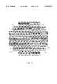
- FIG. 2is diagram illustrating a conventional silicon wafer which includes numerous die.
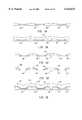
- FIG. 3is diagram illustrating two segments in accordance with the present invention, where each segment includes a two-by-two array of die.
- FIG. 4is a diagram illustrating a plurality of segments laid out across a wafer.
- FIGS. 5A-5Hare cross-sectional views of a portion of a wafer and illustrates the multiple layers of material applied to the wafer in order to interconnect the die of a segment.
- FIGS. 6A and 6Bare diagrams illustrating edge wall profiles of a polyimide layer.
- FIGS. 7A and 7Bare diagrams illustrating the metal lift-off process which provides metal interconnects on a wafer.
- FIG. 8Ais a diagram showing the backside of a segment including four beveled side walls after the segment has been cut from a wafer.
- FIG. 8Bis a diagram showing the front side and the beveled side walls of three segments after being cut from a wafer.
- FIG. 9is a diagram illustrating a segment stacking and gluing procedure in which segments are stacked and epoxied together.
- FIGS. 10A and 10Bare diagrams illustrating a method for providing a vertical electrical path between segments in a stack according to the present invention.
- FIG. 11is a diagram illustrating the mechanism by which epoxy traces are dispensed along the edges of a stack.
- FIG. 12is cross-sectional view of a signal carrying substrate having a plurality of stacks which are subsurface mounted therein in accordance with the present invention.
- FIG. 13is a diagram illustrating a method for electrically connecting a subsurface mounted stack to a circuit board.
- FIG. 14shows a cross sectional view of two layers of a VIP stack mechanically bonded to one another with epoxy where the epoxy includes glass spheres within the epoxy for purposes of maintaining a distance between the layers.
- FIG. 15shows a cross sectional view of a two layers of a VIP stack with thermally conductive epoxy preform containing glass spheres according to the present invention.
- FIG. 16shows a top view of one die and the glass spheres surrounded by epoxy of FIG. 14.
- FIG. 17shows a top view of one die and the thermally conductive epoxy preform of FIG. 15.
- the vertical interconnect processwill be described beginning with a standard wafer 30 which is supplied by a manufacturer.
- the squares on the wafer 30indicate the locations of individual die 32 on the wafer 30.
- Wafers 30normally arrive from the manufacturer with non-functioning or defective die which are marked with an ink dot 34.
- the wafer 30is made of silicon.
- the wafer 30could also be made using alternate materials, such as gallium arsenide.
- the die 32are cut out of the wafer 30 in order to provide a supply individual chips, such as memory chips, for example.
- the die 32are not individually cut out of the wafer 30. Instead, a plurality of adjacent die 32 on the wafer 30 are grouped to form what is referred to as a segment 32, as shown in FIG. 3.
- the diecould be cut individually in accordance with the prior VIP process and with the present invention.
- FIG. 3depicts a plane view of two segments 36A and 36B (hereinafter segments 36) on a wafer 30 where each rectangle represents one die 32.
- Each segment 36is defined by vertical boundary lines 38 and horizontal boundary lines 40 and each segment 36 includes a group of adjacent die 32 on the wafer 30, which results in a segment 36 having a particular size and shape.
- a segment 36includes four adjacent die 32 arranged in a two-by-two matrix, as shown. Such a segment 36 is referred to as a two-by-two segment.
- a segment 36may also include any pattern or arrangement of adjacent die 32, such as for example, a one-by-one segment, two-by-one segment, a two-by-four segment, or a four-by-four segment of die 32.
- Each segment 36is provided with edge bond pads 42 on one or more sides of the segment 36, which are used as electrical contact points for external connections.
- each of the die 32includes internal bond pads 44 for connection with internal circuity of the die 32.
- Individual segments 36are separated from the wafer 30 by cutting the wafer 30 along the vertical boundary lines 38 and horizontal boundary lines 40, which are typically referred to as streets. The process of cutting the segments 36 from the wafer 30 is described further below.
- the die interconnect circuitryincludes a plurality of metal traces which are orientated in both the x and y directions on the surface of the segment 32.
- the metal tracesare referred to as x-interconnects 46 and y-interconnects 48 and function to communicate power and signals from the edge bond pads 42 of the segment 36 to selected internal bond pads 44 of the individual die 32.
- FIG. 4depicts a diagram illustrating a plurality of segments 36 laid out across a wafer 30.
- the bond pads of individual die 32are routed appropriately to create a one-by-one segment 50.
- the ink dots 34(FIG. 2) which indicate defective die must first be removed so that the ink dots 34 do not interfere with the metal interconnects 46 and 48.
- the ink dots 34are removed from the wafer 30 using a conventional positive resist stripper.
- a positive resist stripperis a material commonly used in the industry to dissolve and remove unwanted substances from a particular surface without damaging the original surface.
- the surface of the wafer 30includes a plurality of internal bond pads 44 belonging to individual die 32 (see FIGS. 2 and 3) and a plurality of external bond pads 42 belonging to segments 36.
- a polyimide layer 60is first deposited on the wafer 30, as shown in FIG. 5B.
- the wafer manufacturersprovide a passivation layer on the surface of the wafer 30 that should insulate the circuits, the polyimide layer 60 ensures that there are no holes in the passivation material.
- the polyimide layer 60also helps fill in the streets 38 and 40 (see FIG. 3) between the die 32 on the wafer 30.
- the polyimide layer 60is applied by a standard spin coating process in which polyimide is placed in the middle of the wafer 30 and the wafer 30 is spun horizontally on a spin motor to provide a thin polyimide layer 60 on the wafer 30 that is approximately two microns in thickness.
- the polyimide layer 60is removed from the surface of the wafer 30 over bond pads 44 and 42.
- the polyimide layer 60is removed over the bond pads 44 and 42 using a standard photolithographic process.
- a layer of photo-sensitive materialcalled positive photoresist
- positive photoresistis applied to the surface of the polyimide layer 60 and baked.
- a mask having openings defining the location of the bond pads 44 and 42 on the wafer 30is superimposed on the photoresist using a conventional aligner device.
- the maskis flooded with ultra-violet radiation and the uncovered portions of the photoresist over the bond pads 44 and 42 is exposed to the light.
- the exposed photoresistis then stripped from the surface of the bond pads 44 and 42 and developed in a dilute developer.
- the remaining positive photoresistis removed from the wafer 30 using acetone or other positive photoresist stripper material.
- Acetoneis a material that washes away photoresist but will not damage the polyimide layer 60.
- the wafer 30is baked to cure the polyimide layer 60.
- polyimideis cured for one half-hour at four hundred degrees.
- the polyimide layer 60is cured for six hours at a temperature of three hundred fifty degrees in order to reduce the possibility of harming the circuitry on the wafer 30.
- polyimideis used for the insulation layer 60 which produces rounded edge walls 70 in the areas where the polyimide layer 60 is removed, as shown in FIG. 6A.
- the rounded edge walls 70 of the polyimide layer 60are desirable to facilitate the deposition of a layer metal 48 which will be applied to the polyimide layer 60.
- a photoimageable polyimide 61provides edge walls that have sharp corners 72 which results in a discontinuity in the metal layer 49, as shown in FIG. 6B.
- the next stage of the vertical interconnect processis referred to as the metal lift-off process in which a first metal layer 48 is applied to the wafer 30 to electrically interconnect each of the die 32 located on a segment 36.
- the first metal layer 48 deposited on the wafer 30contacts the bond pads 44 and 42 and corresponds to the metal y-interconnects 48 of FIG. 3.
- the paths of the metal y-interconnects 48 across the wafer 30are defined using a standard photolithographic process.
- the first step of the metal lift-off processis to apply a layer of lift-off photoresist 74 over the polyimide layer 60.
- a commercially available image reversal photoresistis applied to the wafer 30 in a well known manner.
- the photoresist 74is then removed in selected areas to define the paths of the metal y-interconnects 48.
- the image-reversal photoresist 74is removed such that an overhanging edge, which is referred to as a retrograde or re-entrant edge wall 76, is produced along the path of the metal y-interconnects 48 as shown in FIG. 7A.
- the wafer 30is placed into a standard sputtering tool (not shown) which is used to deposit the metal layer 48 over the entire wafer 30.
- the metal layer 48includes a sandwich of chrome, titanium-tungsten, and gold. The chrome and titanium-tungsten are combined with the gold primarily for adhesion purposes, but other metal sandwiches may also be used.
- approximately two thousand angstroms of chrome, five hundred angstroms of titanium-tungsten, and approximately twelve hundred angstroms of goldare deposited on the wafer 30.
- approximately six thousand angstroms of goldare deposited on wafer 30.
- the remaining photoresist 74is removed from the surface of the wafer 30.
- Photoresistis typically removed by soaking the wafer 30 in acetone or other positive photoresist stripper which dissolves the photoresist 74.
- the metal layer 48lifts away from the surface of the first polyimide layer 60 leaving the metal interconnects 48 (see FIG. 3).
- the purpose of the re-entrant edge walls 76is to allow the acetone to flow around the edges of the metal y-interconnects 48 and effectively dissolve the photoresist 74.
- the wafer 30is baked to evaporate the acetone that soaked into the polyimide layer 60. After this step, one layer of gold is left on the surface of the polyimide layer 60 defining the y-interconnects 48 which are in contact with the bond pads 44 and 42, as shown in FIG. 5D.
- a second metal layer 46is provided on the wafer by essentially repeating the process described above.
- the second metal layer 46corresponds to the x-interconnects 46 shown in FIG. 3.
- a second polyimide depositionis performed to provide a second polyimide layer 80 on the wafer 30.
- the second polyimide layer 80is applied in the same manner as the first polyimide layer 60, but need not be as thick. After the second polyimide layer 80 is applied, holes are opened in the second layer 80 over points on the metal y-interconnects 48 which are to electrically contact the metal x-interconnects 46, as shown in FIG. 5F.
- the second polyimide layer 80is also removed from edge bond pads 42 on each segment 36 to allow the second layer of metal interconnects 46 to electrically contact the edge bond pads 42 once the segments 36 are stacked.
- the first metal layer 48may be used to contact the edge bond pads 42 instead of the second metal layer 46.
- the second polyimide layer 80is removed from the selected points on the wafer 30, the second polyimide layer 80 is cured at a low temperature to prevent interaction between the gold interconnects 48 and the aluminum bond pads 44 and 42 which could produce an undesirable insulating substance.
- a second metal lift-off processis performed to form the second layer of interconnects 46, as shown in FIG. 5G.
- an image reversal photoresistis applied to the wafer 30 and the photoresist is removed in places which define the paths of the second layer of gold interconnects 48 on the wafer 30.
- the processyields a layer of photoresist defining paths with re-entrant edge walls.
- a metal layer including a sandwich of chrome, titanium-tungsten, and goldis then sputter deposited on the photoresist. The chrome is unnecessary in the second layer 48 but may be used for standardization of the manufacturing process.
- the lift-off stepis performed to remove the unwanted photoresist and metal, leaving the x-interconnects 46 of FIG. 3.
- a third polyimide layer 90is applied to the wafer 30, as shown in FIG. 5H, to protect the metal x-interconneets 46 from scratches and to act as a mechanical barrier to the outside world.
- the third polyimide layer 90is removed around the edges of each segment 36 to expose the edge bond pads 42 which will later be in electrical contact with the edge bond pads of other segments. Either a conventional photo-imageable polyimide 90 or a nonphoto-imageable is acceptable to protect the metal x-interconnects 46.
- the first polyimide layer 60protects the circuits on the wafer 30 while the first layer of metal interconnects 48 makes contact with the bond pads 44 and 42.
- the second polyimide layer 80insulates the second layer of metal interconnects 48 from the first layer of metal interconnects 46 except where the two layers contact.
- the third polyimide layer 90protects and insulates the second layer of metal interconnects 48.
- the two layers of metal interconnects 46 and 48 provided by the wafer interconnect VIP processadds flexibility in routing lines across the wafer 30 to interconnect the die 32 on each segment 36. Interconnecting the die 32 on a segment 36 and then stacking the segments 36, is less costly and more reliable than the prior art method of cutting individual chips from a wafer 30, stacking the chips, and interconnecting the chips on a circuit board.
- a segment formation processis performed on the wafer 30.
- the wafer 30is divided into individual segments 36 by cutting the wafer 30 along the vertical and horizontal streets 38 and 40 between the segments 36.
- the segmentswill be placed in a stacked structure.
- the segments 36are first thinned by grinding away material from the backside of the segments 36.
- the entire wafer 30is thinned before the segments 36 are cut from the wafer 30. The thinning process reduces the height of the wafer 30 and the segments 36 from a height of approximately twenty-five mils to approximately eight to ten mils.
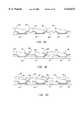
- FIG. 8Ashows the backside 100 of a segment 36 after the segment 36 has been cut from a wafer using a bevel cut. As shown, the bevel cut provides the segment 36 with inwardly sloping edge walls 102 on all four sides of the segment 36.
- a pattern of streets 38 and 40 defining segment boundariesis provided on the backside 100 of the wafer 30 to guide the saw.
- a pattern of the segment boundariesis provided on the backside 100 placing the wafer 30 in a device including a video camera and a felt-tipped writing device.
- the waferis mounted in the device such that the front-side of the wafer 30 faces the camera while the writing device is placed in contact with the backside 100 of the wafer 30.
- the image of the front-side of the wafer 30is displayed on a monitor and an operator moves the wafer 30 beneath the writing device along the pattern of the segment boundaries to draw the patterns on the backside 100 of the wafer 30.
- a pattern of the segment boundariesmay also be provided on the backside 100 of the wafer 30 using a conventional photolithographic process.
- the backside 100 of the wafer 30is coated with photoresist, the front of wafer 30 is illuminated with infrared light such that the circuitry may be seen on the backside 100 of the wafer 30, and a pattern of the segment boundaries is aligned and developed on the surface of the backside 100 of the wafer 30 in order to guide the saw.
- a layer of tapeis applied to the front of wafer 30 to hold the segments 36 together during sawing.
- a bevel cutis performed along the segment boundaries on the backside 100 of the wafer 30.
- the bevel cutproduces segment edge walls 102 having a 45-degree angle.
- FIG. 8Bshows three segments 36 placed in vertical alignment above one another, after the segments are cut from a wafer 30, and just before the segments are assembled permanently into a stack.
- the front side 104 of each segment 36contains the metal interconnects 48 and 46, and the edge bond pads 42.
- the edge bond pads 42 of a segment 36will be in electrical contact with the edge bond pads 42 of vertically adjacent segments 36 in the stack.
- the purpose of the beveled edge walls 102is to provide suitable clearance for a vertical electrical connection between the edge bond pads 42 of one segment 36 and the edge bond pads 42 of the segment 36 immediately below the first in the stack.
- a sputtered nitride processis similar to the sputtering of the metal films, except instead of a metal, a silicon nitride is sputtered onto the backside 100 of the segment 36.
- the silicon nitride insulationis necessary so that noise and interfering signals are not absorbed into the silicon substrate base of the die 32 on segments 36.
- the circuits on the segments 36are tested for functionality. Since a portion of the die 32 on a wafer 30 may not function, and the defective die are not cut from the wafer 30 and discarded as in prior art methods, the defective die must be disconnected from the functioning die 32.
- Defective diemay be disconnected by using a laser to vaporize the top layer of metal interconnects 46 that are connected between the edge bond pads 42 of a segment 36 and the circuits of the defective die. The defective die may also be disconnected by mechanically abrading or electrically fusing the top layer of metal interconnects 46. Once the top layer of metal interconnects 46 has been opened between the edge bond pads 42 of a segment 36 and the circuits of a defective die, the defective die is no longer electrically connected to the segment 36.
- each segment 36is also made unique so that decoding circuitry, which will interface with the finished stack, may access each segment 36.
- each segment 36is made unique during a process called level programming in which a plurality of control signals are burned on each segment using a laser. Referring back to FIG. 3, the plurality of control signals is provided on each segment by burning a unique pattern onto control bond pads 106 on each segment 36, although a unique pattern could also be formed by electrically blowing fuses.
- the segments 36are programmed.
- programmingrefers to the process of routing circuitry so that redundant functional die 32 replace the disconnected defective die. This is done by providing the replacement die 32 with appropriate control signals originally intended for the disconnected die. Programming is necessary because once the segments 36 are stacked and become operative, a computer or the like may attempt to access a disconnected die in the stack. Therefore, the segments 36 which have defective die must be programmed so that when an attempt is made to access a defective die in a stack, a functioning die 32 is accessed instead. The actual programming of the segments 36 occurs during the fabrication of a stack, as described below.
- a segment gluing fixture 110wherein a stack 112 is assembled during a stacking procedure in which the segments 36 are stacked and epoxied together.
- a stack 112is assembled using six adjacent segments 36 to provide six logical levels.
- a stack 112is assembled by providing a film of epoxy 114 between each pair of adjacent segments 36, and then placing the segments 36 front side 104 up in an alignment fixture 116.
- the alignment fixture 116compresses the stack 112 in a horizontal plane against fixed walls of the fixture, and compresses the stack 112 in a vertical plane against the base of the fixture using three closed-cell urethane rubber stamps 118, 119, and 120.
- the stack 112is then cured at one hundred twenty degrees while remaining in the fixture to solidify the stack 112.
- the cure cycleincludes a fifteen minute stabilization period, a sixty minute cure, and a ten minute cool down.
- the VIP processis an improvement over prior methods in which individual die 32 are stacked, because the segments 36 comprising the stack 112 of the present invention may be of varying thickness and may be stacked in any order.
- the edge bond pads 42(see FIG. 8B) on each of the segments 36 is vertically electrically connected in the stack 112 in order to provide an electrically functional stack 112.
- Prior art methods for vertically connecting elements of a stackinclude connecting the elements with metal rods, and providing a plurality of vias in the elements and inserting an electrically conductive material in the vias, or filling the vias with a conductive liquid to provide an electrical path between the elements of the stack.
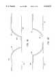
- FIGS. 10A and 10Ba method for providing a vertical electrical path between segments 36 of a stack 112 is shown according to the present invention.
- FIG. 10Adepicts a stack 112 from the backside 100 of the segments 36 with the stack positioned on its side.
- FIG. 10Bdepicts a view of the stack 112 from the front side 104 of the segments 36 where the stack is positioned vertically.
- silvered-filled conductive epoxy traces 130are dispensed by a dispense mechanism 132 along the beveled edge walls 102 of the segments 36.
- the dispense mechanism 132moves in an x- and y-direction and places the epoxy traces on the stack 112 in alignment with the external bond pads 42 of the segments 36.
- the epoxy traces 130are applied to all four edges of the stack 112 in preprogrammed locations and the epoxy traces 130 flow to vertically connect the exposed metal of the bond pads 42.
- the beveled edge walls 102 of the segments 36facilitate access to the external bond pads 42 by the epoxy traces 130.
- the use of beveled edge walls 102 and the epoxy traces 130 of the VIP processis an improvement over prior art methods that use a layer of metallization to provide a vertical electrical connection to a stack.
- the epoxy traces 130are selectively dispensed to different layers of the stack 112 according to preprogramming.
- the various epoxy traces 130define circuit paths of a particular device and also route circuitry around disconnected defective die.
- each location of a die 32 on the segments 36defines a vertical column in the stack 112. For example, if each segment 36 in a stack 112 includes six die 32, the stack 112 include six vertical columns of die 32.
- a functioning circuitsuch as a memory circuit, a certain number of functioning die 32 is required in each vertical column of a segment 36.
- the circuitry of a stack 112 that includes six segmentsis routed during programming to provide four functioning die 32 in each column of the stack.
- a stack of 8-12 adjacent segmentscould be configured to provide eight logical levels of die in each column of the stack.
- the dispensing mechanism 140includes a rotary indexing vacuum chuck 134, a dispense mechanism 132, a sealed rotary vacuum joint 138, a motor 142, and a 90-degree indexing mechanism 144.
- the sealed rotary vacuum joint 138works in conjunction with a vacuum pump (not shown) to create a vacuum at the end of the vacuum chuck 134, which is located beneath the dispense mechanism 132.
- a stack 112is placed horizontally on the vacuum chuck 134, and the chuck 134 holds the stack 112 on its front side 104, via the vacuum.
- the dispense mechanism 132is moved above one edge of the stack 112 to dispense pre-programmed channels of epoxy traces 130 down one side of the stack 112, as described above.
- the dispense mechanism 132is moved away and the vacuum chuck 134 is then rotated 90-degrees by the 90-degree indexing mechanism 144 so that the epoxy may be dispensed along another edge of the stack 112. The process repeats until all the edges of the stack 112 are epoxied.
- the epoxy dispense mechanism 132is a 30 gage, Luer-tipped 5 cc hypodermic syringe having a resolution of one-thousandths of an inch, and is mounted on a programmable robot (not shown).
- the stack 112is removed from the chuck 134 and placed in a holding area with special handling because the epoxy 130 is wet.
- the epoxied segment stacks 112are then placed in a convection oven for curing, which includes a fifteen minute preheat, a sixty minute cure, and a ten minute cool down.
- the stack 112 processis complete and the stack 112 is ready for mounting on a circuit carry substrate, such as a printed circuit board, for example.
- the stack 112can be connected to a circuit board by subsurface mounting the stack 112 in the circuit board.
- FIG. 12a cross-sectional view of a circuit board 150 is shown having a plurality of stacks 112 subsurface mounted therein in accordance with the VIP process.
- a plurality of holes 154slightly larger than the perimeter of the stacks 112 are cut in the circuit board 150. After the holes 154 are cut into the circuit board 150, the circuit board 150 is placed in a clamping fixture 152.
- the stacks 112are then placed in the holes 154 in the circuit board 150 so that the front side 104 of the top segment 36 of the stack 112 is coplaner with the printed circuit board 150, as shown.
- the stacks 112are held in place for forthcoming operations by applying small drops of fast-curing positional epoxy (not shown) at various locations around the perimeter of the stacks 112.
- Subsurface mounting the stacks 112 in a circuit board 150provides numerous advantages which include: allowing for coefficient of thermal expansion, reducing the overall height of the stack 112 on the circuit board 150 so the stacks 112 may be made taller for added density, and simplifying the electrical connection between the stack 112 and the circuit board 150, as will now be described.
- FIG. 13a method for electrically connecting a stack 112 to the circuit board 150 is shown for the prior VIP process.
- the stacks 112are electrically connected to metal traces 160 on the circuit board 150 so that the computer circuitry can access the die 32 on each level of the stack 112.
- Each stack 112is positioned in the circuit board 150 so that the edge bond pads 42 around the perimeter of the top segment 36 match the positions of the metal traces 160 on the circuit board 150.
- silver filled conductive epoxy whiskers 162are applied from each bonding pad 42 to an opposing metal trace 160 on the circuit board 150 using the dispense mechanism 132.
- the positional epoxy 158which is used to affix the stack 112 to the circuit board 150, is applied so as to not interfere with the conductive epoxy whiskers 162.
- One feature of the VIP processis that electrical contact between the stack 112 and the metal traces 160 on the circuit board 150 is made with conductive epoxy whiskers 162 which lie in substantially the same plane as the circuit board 150.
- the horizontal epoxy whiskers 162 of the prior VIP processprovide an electrical connection between the circuit board 150 and the edge bond pads 42 of the top segment 36 in a stack 112, and between the edge bond pads 42 of the top segment 36 and the vertical epoxy traces 130 which were applied down the edges of the stack 112 to interconnect the segments 36.
- the horizontal and vertical conductive epoxy traces 160 and 132 applied to the stack 112enable the circuits of the circuit board 150 to access any segment 36 in the stack 112.
- the board 150 assemblyis placed in a convection oven for a final cure which includes: a fifteen minute preheat, a sixty minute cure, and a fifteen minute cool-down. After the cure, the board 150 assembly may be tested and then encapsulated with a polyimide layer.
- the completed circuit board 150 assembly of the present inventionmay then be used for many purposes, such as in a Personal Computer Memory Card International Association (PCMCIA) card.
- PCMCIAis a small credit card sized device that is inserted into notebook and portable computers to provide additional input/output functions and increased storage.
- the stacks of the VIP processmay be mounted in a PCMCIA card and used as external memory circuits for a notebook computer, for example.
- VIPVertical Interconnect Process
- thermally conductive epoxy preformcould be utilized with the VIP process described above.
- FIG. 14shows a stack made of a VIP process as described in the cross referenced VIP patent application.
- FIG. 16shows a top view of FIG. 14, in which glass spheres 244 are individually placed down on top of die 242 with a small amount of epoxy 246 around each sphere 244.
- the stack of die 240, 242are separated by glass spheres 244 with liquid epoxy 246 around spheres 244.
- the glass spheres 244keep the die 240, 242 from touching one another.
- the glass spheresprovide a means of keeping the die 240, 242 separated by a predetermined distance (e.g., 4-6 mils). This distance provides access between the die 240, 242 to electrically connect to the pads which lie on the plane of the die 240, 242. Without the separation, the two die 240, 242 could touch one another, which would inhibit access between the die.
- Electrically conductive epoxycan be inserted between the die 240, 242 and make contact to a pad.
- the calibrated separation or distance between the dieprovides for insertion of an electrically conductive epoxy, as described above, so as to make an electrical connection.
- FIG. 15shows the thermally conductive epoxy preform feature according to the present invention.
- preformed epoxy 256includes a plurality of glass spheres 254 embedded within the epoxy preform 256.
- the glass spheres 254are randomly distributed within the preform 256.
- One preferred process to form the epoxy preform 256is to stir glass spheres 254 into a liquid epoxy, which is then rolled to form a sheet 256 of thermally conductive epoxy containing glass spheres 254, such as shown in FIG. 15.
- the sheet of thermally conductive epoxy preform 256is sized and placed between die 250, 252 (the epoxy preform 256 is shown separated from the die 250, 252 in FIG. 19 for clarity purposes).
- FIG. 17shows a top view of the thermally conductive epoxy sheath feature of the present invention with the epoxy preform 256 placed on top of die 252.
- Epoxy preform 73has glass spheres 254 embedded within the preform 256.
- the glass spheres 254are preferably randomly distributed within preform 256, as shown in FIG. 17.
- thermally conductive epoxy preformprovides much more package strength so as to distribute forces more evenly.
- thermal aspectsare greatly improved such that the present invention provides a significant thermal improvement to a VIP stack.
- the conductive epoxy preform according to the present inventionis a thermally conductive material such that heat can be removed from between the VIP layers much more efficiently, as contrasted with prior approaches in which air is used as the thermal removal medium, and air has relatively poor thermal conductivity.
- the VIP stackis stronger because the forces are distributed better within the VIP stack. Prior mechanical stresses were concentrated on the individual glass spheres. With the present invention, the conductive epoxy preform allows for forces to be more evenly distributed throughout the stack.
Landscapes
- Engineering & Computer Science (AREA)
- Microelectronics & Electronic Packaging (AREA)
- Power Engineering (AREA)
- Computer Hardware Design (AREA)
- Physics & Mathematics (AREA)
- Condensed Matter Physics & Semiconductors (AREA)
- General Physics & Mathematics (AREA)
- Manufacturing & Machinery (AREA)
- Chemical & Material Sciences (AREA)
- Materials Engineering (AREA)
- Internal Circuitry In Semiconductor Integrated Circuit Devices (AREA)
Abstract
Description
Claims (21)
Priority Applications (6)
| Application Number | Priority Date | Filing Date | Title |
|---|---|---|---|
| US08/918,501US6124633A (en) | 1994-06-23 | 1997-08-22 | Vertical interconnect process for silicon segments with thermally conductive epoxy preform |
| PCT/US1998/016901WO1999010925A1 (en) | 1997-08-22 | 1998-08-14 | Vertical interconnect process for silicon segments with thermally conductive epoxy preform |
| JP2000508139AJP2001514449A (en) | 1997-08-22 | 1998-08-14 | Vertical interconnect method of silicon segments with thermally conductive epoxy preform |
| KR10-2000-7001499AKR100536823B1 (en) | 1997-08-22 | 1998-08-14 | Vertical interconnect process for silicon segments with thermally conductive epoxy preform |
| EP98943211AEP1029346A4 (en) | 1997-08-22 | 1998-08-14 | VERTICAL CONNECTION PROCESS FOR SILICON SEGMENTS WITH THERMAL-LEADING EPOXY COMPONENTS |
| AU91052/98AAU9105298A (en) | 1997-08-22 | 1998-08-14 | Vertical interconnect process for silicon segments with thermally conductive epoxy preform |
Applications Claiming Priority (2)
| Application Number | Priority Date | Filing Date | Title |
|---|---|---|---|
| US08/265,081US5675180A (en) | 1994-06-23 | 1994-06-23 | Vertical interconnect process for silicon segments |
| US08/918,501US6124633A (en) | 1994-06-23 | 1997-08-22 | Vertical interconnect process for silicon segments with thermally conductive epoxy preform |
Related Parent Applications (1)
| Application Number | Title | Priority Date | Filing Date |
|---|---|---|---|
| US08/265,081Continuation-In-PartUS5675180A (en) | 1994-06-23 | 1994-06-23 | Vertical interconnect process for silicon segments |
Publications (1)
| Publication Number | Publication Date |
|---|---|
| US6124633Atrue US6124633A (en) | 2000-09-26 |
Family
ID=46203182
Family Applications (1)
| Application Number | Title | Priority Date | Filing Date |
|---|---|---|---|
| US08/918,501Expired - LifetimeUS6124633A (en) | 1994-06-23 | 1997-08-22 | Vertical interconnect process for silicon segments with thermally conductive epoxy preform |
Country Status (1)
| Country | Link |
|---|---|
| US (1) | US6124633A (en) |
Cited By (23)
| Publication number | Priority date | Publication date | Assignee | Title |
|---|---|---|---|---|
| US20020017709A1 (en)* | 2000-06-07 | 2002-02-14 | Yoshiyuki Yanagisawa | Assembly jig and manufacturing method of multilayer semiconductor device |
| US6451626B1 (en) | 2001-07-27 | 2002-09-17 | Charles W.C. Lin | Three-dimensional stacked semiconductor package |
| US6486549B1 (en) | 2001-11-10 | 2002-11-26 | Bridge Semiconductor Corporation | Semiconductor module with encapsulant base |
| US6528894B1 (en)* | 1996-09-20 | 2003-03-04 | Micron Technology, Inc. | Use of nitrides for flip-chip encapsulation |
| US6548376B2 (en) | 2001-08-30 | 2003-04-15 | Micron Technology, Inc. | Methods of thinning microelectronic workpieces |
| US20030193786A1 (en)* | 2002-04-15 | 2003-10-16 | Ralf Greiner | Compact circuit carrier package |
| US6716670B1 (en) | 2002-01-09 | 2004-04-06 | Bridge Semiconductor Corporation | Method of forming a three-dimensional stacked semiconductor package device |
| US6765287B1 (en) | 2001-07-27 | 2004-07-20 | Charles W. C. Lin | Three-dimensional stacked semiconductor package |
| US20050224952A1 (en)* | 2004-04-13 | 2005-10-13 | Al Vindasius | Three dimensional six surface conformal die coating |
| US20050258530A1 (en)* | 2004-04-13 | 2005-11-24 | Al Vindasius | Micropede stacked die component assembly |
| US7067911B1 (en) | 2000-10-13 | 2006-06-27 | Bridge Semiconductor Corporation | Three-dimensional stacked semiconductor package with metal pillar in encapsulant aperture |
| US20060156540A1 (en)* | 2005-01-18 | 2006-07-20 | Hewlett-Packard Development Company, L.P. | Method for aligning a component on a printed circuit board |
| US7129113B1 (en) | 2000-10-13 | 2006-10-31 | Bridge Semiconductor Corporation | Method of making a three-dimensional stacked semiconductor package with a metal pillar in an encapsulant aperture |
| US7190060B1 (en) | 2002-01-09 | 2007-03-13 | Bridge Semiconductor Corporation | Three-dimensional stacked semiconductor package device with bent and flat leads and method of making same |
| US7215018B2 (en) | 2004-04-13 | 2007-05-08 | Vertical Circuits, Inc. | Stacked die BGA or LGA component assembly |
| US7227249B1 (en) | 2003-12-24 | 2007-06-05 | Bridge Semiconductor Corporation | Three-dimensional stacked semiconductor package with chips on opposite sides of lead |
| US7262082B1 (en) | 2000-10-13 | 2007-08-28 | Bridge Semiconductor Corporation | Method of making a three-dimensional stacked semiconductor package with a metal pillar and a conductive interconnect in an encapsulant aperture |
| US20080112150A1 (en)* | 2006-11-13 | 2008-05-15 | Trident Space & Defense, Llc | Radiation-shielded semiconductor assembly |
| US7494843B1 (en) | 2006-12-26 | 2009-02-24 | Bridge Semiconductor Corporation | Method of making a semiconductor chip assembly with thermal conductor and encapsulant grinding |
| US7811863B1 (en) | 2006-10-26 | 2010-10-12 | Bridge Semiconductor Corporation | Method of making a semiconductor chip assembly with metal pillar and encapsulant grinding and heat sink attachment |
| US20110138477A1 (en)* | 2009-06-12 | 2011-06-09 | Trident Space and Defense, LLC | Location Sensitive Solid State Drive |
| US7993983B1 (en) | 2003-11-17 | 2011-08-09 | Bridge Semiconductor Corporation | Method of making a semiconductor chip assembly with chip and encapsulant grinding |
| US8829677B2 (en) | 2010-10-14 | 2014-09-09 | Invensas Corporation | Semiconductor die having fine pitch electrical interconnects |
Citations (86)
| Publication number | Priority date | Publication date | Assignee | Title |
|---|---|---|---|---|
| US3679941A (en)* | 1969-09-22 | 1972-07-25 | Gen Electric | Composite integrated circuits including semiconductor chips mounted on a common substrate with connections made through a dielectric encapsulator |
| US3691628A (en)* | 1969-10-31 | 1972-09-19 | Gen Electric | Method of fabricating composite integrated circuits |
| US3702025A (en)* | 1969-05-12 | 1972-11-07 | Honeywell Inc | Discretionary interconnection process |
| US3769702A (en)* | 1971-02-01 | 1973-11-06 | Bunker Ramo | 3d-coaxial memory construction and method of making |
| US3813773A (en)* | 1972-09-05 | 1974-06-04 | Bunker Ramo | Method employing precision stamping for fabricating the wafers of a multiwafer electrical circuit structure |
| US3999105A (en)* | 1974-04-19 | 1976-12-21 | International Business Machines Corporation | Liquid encapsulated integrated circuit package |
| EP0010657A1 (en)* | 1978-10-18 | 1980-05-14 | General Electric Company | Selective etching of polymeric materials embodying silicones via reactor plasmas |
| US4300153A (en)* | 1977-09-22 | 1981-11-10 | Sharp Kabushiki Kaisha | Flat shaped semiconductor encapsulation |
| WO1983004141A1 (en)* | 1982-05-06 | 1983-11-24 | James William Harris | Three dimensional integrated circuit structure |
| US4426773A (en)* | 1981-05-15 | 1984-01-24 | General Electric Ceramics, Inc. | Array of electronic packaging substrates |
| US4525921A (en)* | 1981-07-13 | 1985-07-02 | Irvine Sensors Corporation | High-density electronic processing package-structure and fabrication |
| EP0175870A2 (en)* | 1981-01-16 | 1986-04-02 | Mosaic Systems, Inc. | Wafer scale integrated circuit device |
| EP0178227A2 (en)* | 1984-10-05 | 1986-04-16 | Fujitsu Limited | Integrated circuit semiconductor device formed on a wafer |
| US4612083A (en)* | 1984-07-20 | 1986-09-16 | Nec Corporation | Process of fabricating three-dimensional semiconductor device |
| US4613891A (en)* | 1984-02-17 | 1986-09-23 | At&T Bell Laboratories | Packaging microminiature devices |
| US4646128A (en)* | 1980-09-16 | 1987-02-24 | Irvine Sensors Corporation | High-density electronic processing package--structure and fabrication |
| US4659931A (en)* | 1985-05-08 | 1987-04-21 | Grumman Aerospace Corporation | High density multi-layered integrated circuit package |
| US4672737A (en)* | 1984-01-23 | 1987-06-16 | Irvine Sensors Corporation | Detector array module fabrication process |
| US4677528A (en)* | 1984-05-31 | 1987-06-30 | Motorola, Inc. | Flexible printed circuit board having integrated circuit die or the like affixed thereto |
| US4703170A (en)* | 1985-04-12 | 1987-10-27 | Grumman Aerospace Corporation | Infrared focal plane module |
| US4706166A (en)* | 1986-04-25 | 1987-11-10 | Irvine Sensors Corporation | High-density electronic modules--process and product |
| US4761681A (en)* | 1982-09-08 | 1988-08-02 | Texas Instruments Incorporated | Method for fabricating a semiconductor contact and interconnect structure using orientation dependent etching and thermomigration |
| US4764846A (en)* | 1987-01-05 | 1988-08-16 | Irvine Sensors Corporation | High density electronic package comprising stacked sub-modules |
| US4783695A (en)* | 1986-09-26 | 1988-11-08 | General Electric Company | Multichip integrated circuit packaging configuration and method |
| US4801992A (en)* | 1986-12-01 | 1989-01-31 | Motorola Inc. | Three dimensional interconnected integrated circuit |
| US4803595A (en)* | 1986-11-17 | 1989-02-07 | International Business Machines Corporation | Interposer chip technique for making engineering changes between interconnected semiconductor chips |
| US4807021A (en)* | 1986-03-10 | 1989-02-21 | Kabushiki Kaisha Toshiba | Semiconductor device having stacking structure |
| US4827327A (en)* | 1985-04-13 | 1989-05-02 | Fujitsu Limited | Integrated circuit device having stacked conductive layers connecting circuit elements therethrough |
| US4862249A (en)* | 1987-04-17 | 1989-08-29 | Xoc Devices, Inc. | Packaging system for stacking integrated circuits |
| US4894706A (en)* | 1985-02-14 | 1990-01-16 | Nippon Telegraph And Telephone Corporation | Three-dimensional packaging of semiconductor device chips |
| US4897708A (en)* | 1986-07-17 | 1990-01-30 | Laser Dynamics, Inc. | Semiconductor wafer array |
| US4901136A (en)* | 1987-07-14 | 1990-02-13 | General Electric Company | Multi-chip interconnection package |
| US4907128A (en)* | 1988-12-15 | 1990-03-06 | Grumman Aerospace Corporation | Chip to multilevel circuit board bonding |
| FR2638894A1 (en)* | 1988-11-04 | 1990-05-11 | Thomson Csf | Device and method for connecting and fixing components |
| US4939568A (en)* | 1986-03-20 | 1990-07-03 | Fujitsu Limited | Three-dimensional integrated circuit and manufacturing method thereof |
| US4941033A (en)* | 1988-12-27 | 1990-07-10 | Mitsubishi Denki Kabushiki Kaisha | Semiconductor integrated circuit device |
| US4954875A (en)* | 1986-07-17 | 1990-09-04 | Laser Dynamics, Inc. | Semiconductor wafer array with electrically conductive compliant material |
| US4956694A (en)* | 1988-11-04 | 1990-09-11 | Dense-Pac Microsystems, Inc. | Integrated circuit chip stacking |
| US4956695A (en)* | 1989-05-12 | 1990-09-11 | Rockwell International Corporation | Three-dimensional packaging of focal plane assemblies using ceramic spacers |
| US4956746A (en)* | 1989-03-29 | 1990-09-11 | Hughes Aircraft Company | Stacked wafer electronic package |
| US4959749A (en)* | 1989-08-16 | 1990-09-25 | Unisys Corporation | Layered electronic assembly having compensation for chips of different thickness and different I/O lead offsets |
| US4983533A (en)* | 1987-10-28 | 1991-01-08 | Irvine Sensors Corporation | High-density electronic modules - process and product |
| US4989063A (en)* | 1988-12-09 | 1991-01-29 | The United States Of America As Represented By The Secretary Of The Air Force | Hybrid wafer scale microcircuit integration |
| US4996583A (en)* | 1989-02-15 | 1991-02-26 | Matsushita Electric Industrial Co., Ltd. | Stack type semiconductor package |
| US5006923A (en)* | 1989-09-14 | 1991-04-09 | Litton Systems, Inc. | Stackable multilayer substrate for mounting integrated circuits |
| US5013687A (en)* | 1989-07-27 | 1991-05-07 | Grumman Aerospace Corporation | Framed chip hybrid stacked layer assembly |
| US5019943A (en)* | 1990-02-14 | 1991-05-28 | Unisys Corporation | High density chip stack having a zigzag-shaped face which accommodates connections between chips |
| US5025306A (en)* | 1988-08-09 | 1991-06-18 | Texas Instruments Incorporated | Assembly of semiconductor chips |
| US5028986A (en)* | 1987-12-28 | 1991-07-02 | Hitachi, Ltd. | Semiconductor device and semiconductor module with a plurality of stacked semiconductor devices |
| US5032896A (en)* | 1989-08-31 | 1991-07-16 | Hughes Aircraft Company | 3-D integrated circuit assembly employing discrete chips |
| US5055425A (en)* | 1989-06-01 | 1991-10-08 | Hewlett-Packard Company | Stacked solid via formation in integrated circuit systems |
| US5075253A (en)* | 1989-04-12 | 1991-12-24 | Advanced Micro Devices, Inc. | Method of coplanar integration of semiconductor IC devices |
| WO1992003035A1 (en)* | 1990-08-01 | 1992-02-20 | Staktek Corporation | Ultra high density integrated circuit packages, method and apparatus |
| US5093708A (en)* | 1990-08-20 | 1992-03-03 | Grumman Aerospace Corporation | Multilayer integrated circuit module |
| US5104820A (en)* | 1989-07-07 | 1992-04-14 | Irvine Sensors Corporation | Method of fabricating electronic circuitry unit containing stacked IC layers having lead rerouting |
| US5111278A (en)* | 1991-03-27 | 1992-05-05 | Eichelberger Charles W | Three-dimensional multichip module systems |
| US5117282A (en)* | 1990-10-29 | 1992-05-26 | Harris Corporation | Stacked configuration for integrated circuit devices |
| EP0490739A1 (en)* | 1990-12-11 | 1992-06-17 | Thomson-Csf | Interconnection method and device for three-dimensional integrated circuits |
| US5128831A (en)* | 1991-10-31 | 1992-07-07 | Micron Technology, Inc. | High-density electronic package comprising stacked sub-modules which are electrically interconnected by solder-filled vias |
| US5135556A (en)* | 1991-04-08 | 1992-08-04 | Grumman Aerospace Corporation | Method for making fused high density multi-layer integrated circuit module |
| US5138437A (en)* | 1987-07-27 | 1992-08-11 | Mitsubishi Denki Kabushiki Kaisha | Semiconductor integrated circuit device in which integrated circuit units having different functions are stacked in three dimensional manner |
| US5138438A (en)* | 1987-06-24 | 1992-08-11 | Akita Electronics Co. Ltd. | Lead connections means for stacked tab packaged IC chips |
| US5172303A (en)* | 1990-11-23 | 1992-12-15 | Motorola, Inc. | Electronic component assembly |
| US5191404A (en)* | 1989-12-20 | 1993-03-02 | Digital Equipment Corporation | High density memory array packaging |
| US5191405A (en)* | 1988-12-23 | 1993-03-02 | Matsushita Electric Industrial Co., Ltd. | Three-dimensional stacked lsi |
| US5198888A (en)* | 1987-12-28 | 1993-03-30 | Hitachi, Ltd. | Semiconductor stacked device |
| US5200300A (en)* | 1989-06-01 | 1993-04-06 | Hewlett-Packard Company | Methods for forming high density multi-chip carriers |
| US5202754A (en)* | 1991-09-13 | 1993-04-13 | International Business Machines Corporation | Three-dimensional multichip packages and methods of fabrication |
| US5222014A (en)* | 1992-03-02 | 1993-06-22 | Motorola, Inc. | Three-dimensional multi-chip pad array carrier |
| US5221642A (en)* | 1991-08-15 | 1993-06-22 | Staktek Corporation | Lead-on-chip integrated circuit fabrication method |
| US5229647A (en)* | 1991-03-27 | 1993-07-20 | Micron Technology, Inc. | High density data storage using stacked wafers |
| US5231304A (en)* | 1989-07-27 | 1993-07-27 | Grumman Aerospace Corporation | Framed chip hybrid stacked layer assembly |
| EP0558855A2 (en)* | 1992-03-02 | 1993-09-08 | AT&T Corp. | Circuit board stack with novel cross-over cells |
| US5247423A (en)* | 1992-05-26 | 1993-09-21 | Motorola, Inc. | Stacking three dimensional leadless multi-chip module and method for making the same |
| US5259110A (en)* | 1992-04-03 | 1993-11-09 | International Business Machines Corporation | Method for forming a multilayer microelectronic wiring module |
| US5270261A (en)* | 1991-09-13 | 1993-12-14 | International Business Machines Corporation | Three dimensional multichip package methods of fabrication |
| US5270571A (en)* | 1991-10-30 | 1993-12-14 | Amdahl Corporation | Three-dimensional package for semiconductor devices |
| WO1994001887A1 (en)* | 1992-07-07 | 1994-01-20 | Rtb Technology, Inc. | High density memory and method of forming the same |
| US5283107A (en)* | 1991-05-03 | 1994-02-01 | International Business Machines Corporation | Modular multilayer interwiring structure |
| US5311401A (en)* | 1991-07-09 | 1994-05-10 | Hughes Aircraft Company | Stacked chip assembly and manufacturing method therefor |
| US5330359A (en)* | 1993-03-26 | 1994-07-19 | The Whitaker Corporation | Socket for stacking integrated circuit chips |
| US5377077A (en)* | 1990-08-01 | 1994-12-27 | Staktek Corporation | Ultra high density integrated circuit packages method and apparatus |
| US5446620A (en)* | 1990-08-01 | 1995-08-29 | Staktek Corporation | Ultra high density integrated circuit packages |
| US5455740A (en)* | 1994-03-07 | 1995-10-03 | Staktek Corporation | Bus communication system for stacked high density integrated circuit packages |
| US5475920A (en)* | 1990-08-01 | 1995-12-19 | Burns; Carmen D. | Method of assembling ultra high density integrated circuit packages |
| US5499160A (en)* | 1990-08-01 | 1996-03-12 | Staktek Corporation | High density integrated circuit module with snap-on rail assemblies |
- 1997
- 1997-08-22USUS08/918,501patent/US6124633A/ennot_activeExpired - Lifetime
Patent Citations (96)
| Publication number | Priority date | Publication date | Assignee | Title |
|---|---|---|---|---|
| US3702025A (en)* | 1969-05-12 | 1972-11-07 | Honeywell Inc | Discretionary interconnection process |
| US3679941A (en)* | 1969-09-22 | 1972-07-25 | Gen Electric | Composite integrated circuits including semiconductor chips mounted on a common substrate with connections made through a dielectric encapsulator |
| US3691628A (en)* | 1969-10-31 | 1972-09-19 | Gen Electric | Method of fabricating composite integrated circuits |
| US3769702A (en)* | 1971-02-01 | 1973-11-06 | Bunker Ramo | 3d-coaxial memory construction and method of making |
| US3813773A (en)* | 1972-09-05 | 1974-06-04 | Bunker Ramo | Method employing precision stamping for fabricating the wafers of a multiwafer electrical circuit structure |
| US3999105A (en)* | 1974-04-19 | 1976-12-21 | International Business Machines Corporation | Liquid encapsulated integrated circuit package |
| US4300153A (en)* | 1977-09-22 | 1981-11-10 | Sharp Kabushiki Kaisha | Flat shaped semiconductor encapsulation |
| EP0010657A1 (en)* | 1978-10-18 | 1980-05-14 | General Electric Company | Selective etching of polymeric materials embodying silicones via reactor plasmas |
| US4646128A (en)* | 1980-09-16 | 1987-02-24 | Irvine Sensors Corporation | High-density electronic processing package--structure and fabrication |
| EP0175870A2 (en)* | 1981-01-16 | 1986-04-02 | Mosaic Systems, Inc. | Wafer scale integrated circuit device |
| US4426773A (en)* | 1981-05-15 | 1984-01-24 | General Electric Ceramics, Inc. | Array of electronic packaging substrates |
| US4525921A (en)* | 1981-07-13 | 1985-07-02 | Irvine Sensors Corporation | High-density electronic processing package-structure and fabrication |
| WO1983004141A1 (en)* | 1982-05-06 | 1983-11-24 | James William Harris | Three dimensional integrated circuit structure |
| US4761681A (en)* | 1982-09-08 | 1988-08-02 | Texas Instruments Incorporated | Method for fabricating a semiconductor contact and interconnect structure using orientation dependent etching and thermomigration |
| US4672737A (en)* | 1984-01-23 | 1987-06-16 | Irvine Sensors Corporation | Detector array module fabrication process |
| US4613891A (en)* | 1984-02-17 | 1986-09-23 | At&T Bell Laboratories | Packaging microminiature devices |
| US4677528A (en)* | 1984-05-31 | 1987-06-30 | Motorola, Inc. | Flexible printed circuit board having integrated circuit die or the like affixed thereto |
| US4612083A (en)* | 1984-07-20 | 1986-09-16 | Nec Corporation | Process of fabricating three-dimensional semiconductor device |
| EP0178227A2 (en)* | 1984-10-05 | 1986-04-16 | Fujitsu Limited | Integrated circuit semiconductor device formed on a wafer |
| US4894706A (en)* | 1985-02-14 | 1990-01-16 | Nippon Telegraph And Telephone Corporation | Three-dimensional packaging of semiconductor device chips |
| US4703170A (en)* | 1985-04-12 | 1987-10-27 | Grumman Aerospace Corporation | Infrared focal plane module |
| US4827327A (en)* | 1985-04-13 | 1989-05-02 | Fujitsu Limited | Integrated circuit device having stacked conductive layers connecting circuit elements therethrough |
| US4659931A (en)* | 1985-05-08 | 1987-04-21 | Grumman Aerospace Corporation | High density multi-layered integrated circuit package |
| US4807021A (en)* | 1986-03-10 | 1989-02-21 | Kabushiki Kaisha Toshiba | Semiconductor device having stacking structure |
| US4939568A (en)* | 1986-03-20 | 1990-07-03 | Fujitsu Limited | Three-dimensional integrated circuit and manufacturing method thereof |
| US4706166A (en)* | 1986-04-25 | 1987-11-10 | Irvine Sensors Corporation | High-density electronic modules--process and product |
| US4954875A (en)* | 1986-07-17 | 1990-09-04 | Laser Dynamics, Inc. | Semiconductor wafer array with electrically conductive compliant material |
| US4897708A (en)* | 1986-07-17 | 1990-01-30 | Laser Dynamics, Inc. | Semiconductor wafer array |
| US4783695A (en)* | 1986-09-26 | 1988-11-08 | General Electric Company | Multichip integrated circuit packaging configuration and method |
| US4803595A (en)* | 1986-11-17 | 1989-02-07 | International Business Machines Corporation | Interposer chip technique for making engineering changes between interconnected semiconductor chips |
| US4801992A (en)* | 1986-12-01 | 1989-01-31 | Motorola Inc. | Three dimensional interconnected integrated circuit |
| US4764846A (en)* | 1987-01-05 | 1988-08-16 | Irvine Sensors Corporation | High density electronic package comprising stacked sub-modules |
| US4862249A (en)* | 1987-04-17 | 1989-08-29 | Xoc Devices, Inc. | Packaging system for stacking integrated circuits |
| US5138438A (en)* | 1987-06-24 | 1992-08-11 | Akita Electronics Co. Ltd. | Lead connections means for stacked tab packaged IC chips |
| US4901136A (en)* | 1987-07-14 | 1990-02-13 | General Electric Company | Multi-chip interconnection package |
| US5138437A (en)* | 1987-07-27 | 1992-08-11 | Mitsubishi Denki Kabushiki Kaisha | Semiconductor integrated circuit device in which integrated circuit units having different functions are stacked in three dimensional manner |
| US4983533A (en)* | 1987-10-28 | 1991-01-08 | Irvine Sensors Corporation | High-density electronic modules - process and product |
| US5198888A (en)* | 1987-12-28 | 1993-03-30 | Hitachi, Ltd. | Semiconductor stacked device |
| US5028986A (en)* | 1987-12-28 | 1991-07-02 | Hitachi, Ltd. | Semiconductor device and semiconductor module with a plurality of stacked semiconductor devices |
| US5025306A (en)* | 1988-08-09 | 1991-06-18 | Texas Instruments Incorporated | Assembly of semiconductor chips |
| FR2638894A1 (en)* | 1988-11-04 | 1990-05-11 | Thomson Csf | Device and method for connecting and fixing components |
| US4956694A (en)* | 1988-11-04 | 1990-09-11 | Dense-Pac Microsystems, Inc. | Integrated circuit chip stacking |
| US4989063A (en)* | 1988-12-09 | 1991-01-29 | The United States Of America As Represented By The Secretary Of The Air Force | Hybrid wafer scale microcircuit integration |
| US4907128A (en)* | 1988-12-15 | 1990-03-06 | Grumman Aerospace Corporation | Chip to multilevel circuit board bonding |
| US5191405A (en)* | 1988-12-23 | 1993-03-02 | Matsushita Electric Industrial Co., Ltd. | Three-dimensional stacked lsi |
| US4941033A (en)* | 1988-12-27 | 1990-07-10 | Mitsubishi Denki Kabushiki Kaisha | Semiconductor integrated circuit device |
| US4996583A (en)* | 1989-02-15 | 1991-02-26 | Matsushita Electric Industrial Co., Ltd. | Stack type semiconductor package |
| US4956746A (en)* | 1989-03-29 | 1990-09-11 | Hughes Aircraft Company | Stacked wafer electronic package |
| US5075253A (en)* | 1989-04-12 | 1991-12-24 | Advanced Micro Devices, Inc. | Method of coplanar integration of semiconductor IC devices |
| US4956695A (en)* | 1989-05-12 | 1990-09-11 | Rockwell International Corporation | Three-dimensional packaging of focal plane assemblies using ceramic spacers |
| US5055425A (en)* | 1989-06-01 | 1991-10-08 | Hewlett-Packard Company | Stacked solid via formation in integrated circuit systems |
| US5200300A (en)* | 1989-06-01 | 1993-04-06 | Hewlett-Packard Company | Methods for forming high density multi-chip carriers |
| US5104820A (en)* | 1989-07-07 | 1992-04-14 | Irvine Sensors Corporation | Method of fabricating electronic circuitry unit containing stacked IC layers having lead rerouting |
| US5231304A (en)* | 1989-07-27 | 1993-07-27 | Grumman Aerospace Corporation | Framed chip hybrid stacked layer assembly |
| US5013687A (en)* | 1989-07-27 | 1991-05-07 | Grumman Aerospace Corporation | Framed chip hybrid stacked layer assembly |
| US4959749A (en)* | 1989-08-16 | 1990-09-25 | Unisys Corporation | Layered electronic assembly having compensation for chips of different thickness and different I/O lead offsets |
| US5032896A (en)* | 1989-08-31 | 1991-07-16 | Hughes Aircraft Company | 3-D integrated circuit assembly employing discrete chips |
| US5006923A (en)* | 1989-09-14 | 1991-04-09 | Litton Systems, Inc. | Stackable multilayer substrate for mounting integrated circuits |
| US5191404A (en)* | 1989-12-20 | 1993-03-02 | Digital Equipment Corporation | High density memory array packaging |
| US5019943A (en)* | 1990-02-14 | 1991-05-28 | Unisys Corporation | High density chip stack having a zigzag-shaped face which accommodates connections between chips |
| US5377077A (en)* | 1990-08-01 | 1994-12-27 | Staktek Corporation | Ultra high density integrated circuit packages method and apparatus |
| US5499160A (en)* | 1990-08-01 | 1996-03-12 | Staktek Corporation | High density integrated circuit module with snap-on rail assemblies |
| US5279029A (en)* | 1990-08-01 | 1994-01-18 | Staktek Corporation | Ultra high density integrated circuit packages method |
| US5420751A (en)* | 1990-08-01 | 1995-05-30 | Staktek Corporation | Ultra high density modular integrated circuit package |
| WO1992003035A1 (en)* | 1990-08-01 | 1992-02-20 | Staktek Corporation | Ultra high density integrated circuit packages, method and apparatus |
| US5446620A (en)* | 1990-08-01 | 1995-08-29 | Staktek Corporation | Ultra high density integrated circuit packages |
| US5566051A (en)* | 1990-08-01 | 1996-10-15 | Staktek Corporation | Ultra high density integrated circuit packages method and apparatus |
| US5475920A (en)* | 1990-08-01 | 1995-12-19 | Burns; Carmen D. | Method of assembling ultra high density integrated circuit packages |
| US5561591A (en)* | 1990-08-01 | 1996-10-01 | Staktek Corporation | Multi-signal rail assembly with impedance control for a three-dimensional high density integrated circuit package |
| US5550711A (en)* | 1990-08-01 | 1996-08-27 | Staktek Corporation | Ultra high density integrated circuit packages |
| US5543664A (en)* | 1990-08-01 | 1996-08-06 | Staktek Corporation | Ultra high density integrated circuit package |
| US5093708A (en)* | 1990-08-20 | 1992-03-03 | Grumman Aerospace Corporation | Multilayer integrated circuit module |
| US5117282A (en)* | 1990-10-29 | 1992-05-26 | Harris Corporation | Stacked configuration for integrated circuit devices |
| US5172303A (en)* | 1990-11-23 | 1992-12-15 | Motorola, Inc. | Electronic component assembly |
| EP0490739A1 (en)* | 1990-12-11 | 1992-06-17 | Thomson-Csf | Interconnection method and device for three-dimensional integrated circuits |
| US5229647A (en)* | 1991-03-27 | 1993-07-20 | Micron Technology, Inc. | High density data storage using stacked wafers |
| US5111278A (en)* | 1991-03-27 | 1992-05-05 | Eichelberger Charles W | Three-dimensional multichip module systems |
| US5135556A (en)* | 1991-04-08 | 1992-08-04 | Grumman Aerospace Corporation | Method for making fused high density multi-layer integrated circuit module |
| US5283107A (en)* | 1991-05-03 | 1994-02-01 | International Business Machines Corporation | Modular multilayer interwiring structure |
| WO1993000703A1 (en)* | 1991-06-24 | 1993-01-07 | Irvine Sensors Corporation | Fabricating electronic circuitry unit containing stacked ic layers having lead rerouting |
| US5311401A (en)* | 1991-07-09 | 1994-05-10 | Hughes Aircraft Company | Stacked chip assembly and manufacturing method therefor |
| US5221642A (en)* | 1991-08-15 | 1993-06-22 | Staktek Corporation | Lead-on-chip integrated circuit fabrication method |
| US5270261A (en)* | 1991-09-13 | 1993-12-14 | International Business Machines Corporation | Three dimensional multichip package methods of fabrication |
| US5202754A (en)* | 1991-09-13 | 1993-04-13 | International Business Machines Corporation | Three-dimensional multichip packages and methods of fabrication |
| US5270571A (en)* | 1991-10-30 | 1993-12-14 | Amdahl Corporation | Three-dimensional package for semiconductor devices |
| US5128831A (en)* | 1991-10-31 | 1992-07-07 | Micron Technology, Inc. | High-density electronic package comprising stacked sub-modules which are electrically interconnected by solder-filled vias |
| EP0558855A2 (en)* | 1992-03-02 | 1993-09-08 | AT&T Corp. | Circuit board stack with novel cross-over cells |
| US5222014A (en)* | 1992-03-02 | 1993-06-22 | Motorola, Inc. | Three-dimensional multi-chip pad array carrier |
| US5259110A (en)* | 1992-04-03 | 1993-11-09 | International Business Machines Corporation | Method for forming a multilayer microelectronic wiring module |
| US5247423A (en)* | 1992-05-26 | 1993-09-21 | Motorola, Inc. | Stacking three dimensional leadless multi-chip module and method for making the same |
| WO1994001887A1 (en)* | 1992-07-07 | 1994-01-20 | Rtb Technology, Inc. | High density memory and method of forming the same |
| US5330359A (en)* | 1993-03-26 | 1994-07-19 | The Whitaker Corporation | Socket for stacking integrated circuit chips |
| US5479318A (en)* | 1994-03-07 | 1995-12-26 | Staktek Corporation | Bus communication system for stacked high density integrated circuit packages with trifurcated distal lead ends |
| US5493476A (en)* | 1994-03-07 | 1996-02-20 | Staktek Corporation | Bus communication system for stacked high density integrated circuit packages with bifurcated distal lead ends |
| US5455740A (en)* | 1994-03-07 | 1995-10-03 | Staktek Corporation | Bus communication system for stacked high density integrated circuit packages |
| US5552963A (en)* | 1994-03-07 | 1996-09-03 | Staktek Corporation | Bus communication system for stacked high density integrated circuit packages |
Non-Patent Citations (4)
| Title |
|---|
| Conte, Al S. "MCM-LThe Answer for Desktop Workstations," ICEMM Proceedings, (1993), pp. 18-21. |
| Conte, Al S. MCM LThe Answer for Desktop Workstations, ICEMM Proceedings , (1993), pp. 18 21.* |
| Wojnarowski, R.J., et al. "Three Dimensional Hybrid Wafer Scale Integration Using the GE High Density Interconnect Process," IEEE International Conference on Wafer Scale Integration, Jan. 20, 1993. |
| Wojnarowski, R.J., et al. Three Dimensional Hybrid Wafer Scale Integration Using the GE High Density Interconnect Process, IEEE International Conference on Wafer Scale Integration , Jan. 20, 1993.* |
Cited By (39)
| Publication number | Priority date | Publication date | Assignee | Title |
|---|---|---|---|---|
| US6972249B2 (en) | 1996-09-20 | 2005-12-06 | Micron Technology, Inc. | Use of nitrides for flip-chip encapsulation |
| US6528894B1 (en)* | 1996-09-20 | 2003-03-04 | Micron Technology, Inc. | Use of nitrides for flip-chip encapsulation |
| US20030137062A1 (en)* | 1996-09-20 | 2003-07-24 | Salman Akram | Use of nitrides for flip-chip encapsulation |
| US20020017709A1 (en)* | 2000-06-07 | 2002-02-14 | Yoshiyuki Yanagisawa | Assembly jig and manufacturing method of multilayer semiconductor device |
| US7067911B1 (en) | 2000-10-13 | 2006-06-27 | Bridge Semiconductor Corporation | Three-dimensional stacked semiconductor package with metal pillar in encapsulant aperture |
| US7262082B1 (en) | 2000-10-13 | 2007-08-28 | Bridge Semiconductor Corporation | Method of making a three-dimensional stacked semiconductor package with a metal pillar and a conductive interconnect in an encapsulant aperture |
| US7129113B1 (en) | 2000-10-13 | 2006-10-31 | Bridge Semiconductor Corporation | Method of making a three-dimensional stacked semiconductor package with a metal pillar in an encapsulant aperture |
| US6509639B1 (en) | 2001-07-27 | 2003-01-21 | Charles W. C. Lin | Three-dimensional stacked semiconductor package |
| US6765287B1 (en) | 2001-07-27 | 2004-07-20 | Charles W. C. Lin | Three-dimensional stacked semiconductor package |
| US6794741B1 (en) | 2001-07-27 | 2004-09-21 | Bridge Semiconductor Corporation | Three-dimensional stacked semiconductor package with pillars in pillar cavities |
| US6451626B1 (en) | 2001-07-27 | 2002-09-17 | Charles W.C. Lin | Three-dimensional stacked semiconductor package |
| US6548376B2 (en) | 2001-08-30 | 2003-04-15 | Micron Technology, Inc. | Methods of thinning microelectronic workpieces |
| US6486549B1 (en) | 2001-11-10 | 2002-11-26 | Bridge Semiconductor Corporation | Semiconductor module with encapsulant base |
| US6716670B1 (en) | 2002-01-09 | 2004-04-06 | Bridge Semiconductor Corporation | Method of forming a three-dimensional stacked semiconductor package device |
| US7190060B1 (en) | 2002-01-09 | 2007-03-13 | Bridge Semiconductor Corporation | Three-dimensional stacked semiconductor package device with bent and flat leads and method of making same |
| US7754976B2 (en)* | 2002-04-15 | 2010-07-13 | Hamilton Sundstrand Corporation | Compact circuit carrier package |
| US20030193786A1 (en)* | 2002-04-15 | 2003-10-16 | Ralf Greiner | Compact circuit carrier package |
| US7993983B1 (en) | 2003-11-17 | 2011-08-09 | Bridge Semiconductor Corporation | Method of making a semiconductor chip assembly with chip and encapsulant grinding |
| US7227249B1 (en) | 2003-12-24 | 2007-06-05 | Bridge Semiconductor Corporation | Three-dimensional stacked semiconductor package with chips on opposite sides of lead |
| US7215018B2 (en) | 2004-04-13 | 2007-05-08 | Vertical Circuits, Inc. | Stacked die BGA or LGA component assembly |
| US20050224952A1 (en)* | 2004-04-13 | 2005-10-13 | Al Vindasius | Three dimensional six surface conformal die coating |
| US20070252262A1 (en)* | 2004-04-13 | 2007-11-01 | Vertical Circuits, Inc. | Die Assembly Having Electrical Interconnect |
| US20070284716A1 (en)* | 2004-04-13 | 2007-12-13 | Vertical Circuits, Inc. | Assembly Having Stacked Die Mounted On Substrate |
| US7245021B2 (en) | 2004-04-13 | 2007-07-17 | Vertical Circuits, Inc. | Micropede stacked die component assembly |
| US8729690B2 (en) | 2004-04-13 | 2014-05-20 | Invensas Corporation | Assembly having stacked die mounted on substrate |
| US7535109B2 (en) | 2004-04-13 | 2009-05-19 | Vertical Circuits, Inc. | Die assembly having electrical interconnect |
| US7705432B2 (en) | 2004-04-13 | 2010-04-27 | Vertical Circuits, Inc. | Three dimensional six surface conformal die coating |
| US20050258530A1 (en)* | 2004-04-13 | 2005-11-24 | Al Vindasius | Micropede stacked die component assembly |
| US8357999B2 (en) | 2004-04-13 | 2013-01-22 | Vertical Circuits (Assignment For The Benefit Of Creditors), Llc | Assembly having stacked die mounted on substrate |
| US20060156540A1 (en)* | 2005-01-18 | 2006-07-20 | Hewlett-Packard Development Company, L.P. | Method for aligning a component on a printed circuit board |
| US7811863B1 (en) | 2006-10-26 | 2010-10-12 | Bridge Semiconductor Corporation | Method of making a semiconductor chip assembly with metal pillar and encapsulant grinding and heat sink attachment |
| US20080112150A1 (en)* | 2006-11-13 | 2008-05-15 | Trident Space & Defense, Llc | Radiation-shielded semiconductor assembly |
| US8154881B2 (en) | 2006-11-13 | 2012-04-10 | Telecommunication Systems, Inc. | Radiation-shielded semiconductor assembly |
| US7494843B1 (en) | 2006-12-26 | 2009-02-24 | Bridge Semiconductor Corporation | Method of making a semiconductor chip assembly with thermal conductor and encapsulant grinding |
| US20110138477A1 (en)* | 2009-06-12 | 2011-06-09 | Trident Space and Defense, LLC | Location Sensitive Solid State Drive |
| US8533853B2 (en) | 2009-06-12 | 2013-09-10 | Telecommunication Systems, Inc. | Location sensitive solid state drive |
| US9229880B2 (en) | 2009-06-12 | 2016-01-05 | Telecommunication Systems, Inc. | Location sensitive solid state drive |
| US9361245B2 (en) | 2009-06-12 | 2016-06-07 | Telecommunication Systems, Inc. | Location sensitive solid state drive |
| US8829677B2 (en) | 2010-10-14 | 2014-09-09 | Invensas Corporation | Semiconductor die having fine pitch electrical interconnects |
Similar Documents
| Publication | Publication Date | Title |
|---|---|---|
| US5891761A (en) | Method for forming vertical interconnect process for silicon segments with thermally conductive epoxy preform | |
| US5675180A (en) | Vertical interconnect process for silicon segments | |
| US6255726B1 (en) | Vertical interconnect process for silicon segments with dielectric isolation | |
| US6080596A (en) | Method for forming vertical interconnect process for silicon segments with dielectric isolation | |
| US6124633A (en) | Vertical interconnect process for silicon segments with thermally conductive epoxy preform | |
| US6098278A (en) | Method for forming conductive epoxy flip-chip on chip | |
| US6271598B1 (en) | Conductive epoxy flip-chip on chip | |
| KR100593567B1 (en) | Vertical Interconnect Process for Silicon Segments with Dielectric Insulation | |
| US4953005A (en) | Packaging system for stacking integrated circuits | |
| US4862249A (en) | Packaging system for stacking integrated circuits | |
| US6355976B1 (en) | Three-dimensional packaging technology for multi-layered integrated circuits | |
| US5994170A (en) | Silicon segment programming method | |
| US6933172B2 (en) | Semiconductor wafer with spacer and its manufacturing method, semiconductor device and its manufacturing method, and circuit substrate and electronic device | |
| US20060008944A1 (en) | Substrate having built-in semiconductor apparatus and manufacturing method thereof | |
| EP1029346A1 (en) | Vertical interconnect process for silicon segments with thermally conductive epoxy preform | |
| US7915079B1 (en) | Method of manufacturing layered chip package | |
| EP1135802A1 (en) | Three-dimensional packaging technology for multi-layered integrated circuits | |
| JPH07202115A (en) | Manufacturing of semiconductor devices | |
| JP2002289632A (en) | Method of manufacturing semiconductor device and semiconductor device |
Legal Events
| Date | Code | Title | Description |
|---|---|---|---|
| AS | Assignment | Owner name:ABBOTT LABORATORIES, ILLINOIS Free format text:ASSIGNMENT OF ASSIGNORS INTEREST;ASSIGNOR:BLACK, LAWRENCE A.;REEL/FRAME:009148/0743 Effective date:19980209 | |
| AS | Assignment | Owner name:CUBIC MEMORY, INC., CALIFORNIA Free format text:ASSIGNMENT OF ASSIGNORS INTEREST;ASSIGNORS:VINDASIUS, ALFONS;SAUTTER, KENNETH M.;REEL/FRAME:009051/0093;SIGNING DATES FROM 19980129 TO 19980203 | |
| STCF | Information on status: patent grant | Free format text:PATENTED CASE | |
| FPAY | Fee payment | Year of fee payment:4 | |
| AS | Assignment | Owner name:SILICON VALLEY BANK, CALIFORNIA Free format text:SECURITY INTEREST;ASSIGNOR:VERTICAL CIRCUITS, INC.;REEL/FRAME:015271/0057 Effective date:20021120 | |
| FEPP | Fee payment procedure | Free format text:PAT HOLDER NO LONGER CLAIMS SMALL ENTITY STATUS, ENTITY STATUS SET TO UNDISCOUNTED (ORIGINAL EVENT CODE: STOL); ENTITY STATUS OF PATENT OWNER: LARGE ENTITY | |
| AS | Assignment | Owner name:SILICON VALLEY BANK, CALIFORNIA Free format text:SECURITY AGREEMENT;ASSIGNOR:VERTICAL CIRCUITS, INC.;REEL/FRAME:019910/0394 Effective date:20070905 Owner name:SILICON VALLEY BANK,CALIFORNIA Free format text:SECURITY AGREEMENT;ASSIGNOR:VERTICAL CIRCUITS, INC.;REEL/FRAME:019910/0394 Effective date:20070905 | |
| FEPP | Fee payment procedure | Free format text:ENTITY STATUS SET TO UNDISCOUNTED (ORIGINAL EVENT CODE: BIG.); ENTITY STATUS OF PATENT OWNER: LARGE ENTITY | |
| FPAY | Fee payment | Year of fee payment:8 | |
| REMI | Maintenance fee reminder mailed | ||
| AS | Assignment | Owner name:VERTICAL CIRCUITS, INC., CALIFORNIA Free format text:RELEASE;ASSIGNOR:SILICON VALLEY BANK;REEL/FRAME:023148/0163 Effective date:20090824 Owner name:VERTICAL CIRCULTS, INC., CALIFORNIA Free format text:RELEASE;ASSIGNOR:SILICON VALLEY BANK;REEL/FRAME:023148/0183 Effective date:20090824 Owner name:VERTICAL CIRCUITS, INC.,CALIFORNIA Free format text:RELEASE;ASSIGNOR:SILICON VALLEY BANK;REEL/FRAME:023148/0163 Effective date:20090824 | |
| FPAY | Fee payment | Year of fee payment:12 | |
| AS | Assignment | Owner name:VERTICAL CIRCUITS (ASSIGNMENT FOR THE BENEFIT OF C Free format text:ASSIGNMENT OF ASSIGNORS INTEREST;ASSIGNOR:VERTICAL CIRCUITS, INC.;REEL/FRAME:029186/0755 Effective date:20121023 | |
| AS | Assignment | Owner name:VERTICAL CIRCUITS, INC., DELAWARE Free format text:CHANGE OF NAME;ASSIGNOR:CUBIC MEMORY, INC.;REEL/FRAME:029674/0462 Effective date:19991021 | |
| AS | Assignment | Owner name:VERTICAL CIRCUITS SOLUTIONS, INC., CALIFORNIA Free format text:ASSIGNMENT OF ASSIGNORS INTEREST;ASSIGNOR:VERTICAL CIRCUITS, INC.;REEL/FRAME:029683/0797 Effective date:20121114 | |
| AS | Assignment | Owner name:VERTICAL CIRCUITS, INC., CALIFORNIA Free format text:CHANGE OF NAME;ASSIGNOR:VERTICAL CIRCUITS SOLUTIONS, INC.;REEL/FRAME:029686/0255 Effective date:20070912 | |
| AS | Assignment | Owner name:INVENSAS CORPORATION, CALIFORNIA Free format text:ASSIGNMENT OF ASSIGNORS INTEREST;ASSIGNOR:VERTICAL CIRCUITS (ASSIGNMENT FOR THE BENEFIT OF CREDITORS), LLC;REEL/FRAME:029736/0944 Effective date:20121109 |