US6122198A - Bit by bit APDE verify for flash memory applications - Google Patents
Bit by bit APDE verify for flash memory applicationsDownload PDFInfo
- Publication number
- US6122198A US6122198AUS09/413,182US41318299AUS6122198AUS 6122198 AUS6122198 AUS 6122198AUS 41318299 AUS41318299 AUS 41318299AUS 6122198 AUS6122198 AUS 6122198A
- Authority
- US
- United States
- Prior art keywords
- cell
- overerase
- array
- erase
- memory cell
- Prior art date
- Legal status (The legal status is an assumption and is not a legal conclusion. Google has not performed a legal analysis and makes no representation as to the accuracy of the status listed.)
- Expired - Lifetime
Links
- 101100216008Gallus gallus ANPEP geneProteins0.000titledescription2
- 238000000034methodMethods0.000claimsabstractdescription71
- 230000008901benefitEffects0.000description5
- 238000012986modificationMethods0.000description4
- 230000004048modificationEffects0.000description4
- 239000004065semiconductorSubstances0.000description3
- 239000002784hot electronSubstances0.000description2
- 230000008569processEffects0.000description2
- 230000005689Fowler Nordheim tunnelingEffects0.000description1
- 230000004888barrier functionEffects0.000description1
- 239000000872bufferSubstances0.000description1
- 238000010586diagramMethods0.000description1
- 230000000694effectsEffects0.000description1
- 238000002347injectionMethods0.000description1
- 239000007924injectionSubstances0.000description1
- 230000007246mechanismEffects0.000description1
- QHGVXILFMXYDRS-UHFFFAOYSA-NpyraclofosChemical compoundC1=C(OP(=O)(OCC)SCCC)C=NN1C1=CC=C(Cl)C=C1QHGVXILFMXYDRS-UHFFFAOYSA-N0.000description1
Images


Classifications
- G—PHYSICS
- G11—INFORMATION STORAGE
- G11C—STATIC STORES
- G11C16/00—Erasable programmable read-only memories
- G11C16/02—Erasable programmable read-only memories electrically programmable
- G11C16/06—Auxiliary circuits, e.g. for writing into memory
- G11C16/34—Determination of programming status, e.g. threshold voltage, overprogramming or underprogramming, retention
- G11C16/3404—Convergence or correction of memory cell threshold voltages; Repair or recovery of overerased or overprogrammed cells
- G11C16/3409—Circuits or methods to recover overerased nonvolatile memory cells detected during erase verification, usually by means of a "soft" programming step
- G—PHYSICS
- G11—INFORMATION STORAGE
- G11C—STATIC STORES
- G11C16/00—Erasable programmable read-only memories
- G11C16/02—Erasable programmable read-only memories electrically programmable
- G11C16/06—Auxiliary circuits, e.g. for writing into memory
- G11C16/34—Determination of programming status, e.g. threshold voltage, overprogramming or underprogramming, retention
- G11C16/3404—Convergence or correction of memory cell threshold voltages; Repair or recovery of overerased or overprogrammed cells
- G—PHYSICS
- G11—INFORMATION STORAGE
- G11C—STATIC STORES
- G11C16/00—Erasable programmable read-only memories
- G11C16/02—Erasable programmable read-only memories electrically programmable
- G11C16/06—Auxiliary circuits, e.g. for writing into memory
- G11C16/34—Determination of programming status, e.g. threshold voltage, overprogramming or underprogramming, retention
- G11C16/3436—Arrangements for verifying correct programming or erasure
- G11C16/344—Arrangements for verifying correct erasure or for detecting overerased cells
- G11C16/3445—Circuits or methods to verify correct erasure of nonvolatile memory cells
Definitions
- This inventionrelates generally to a semiconductor integrated circuit memory device that includes an array of flash EEPROM memory cells. More specifically, this invention relates to a semiconductor integrated circuit memory device that includes an array of flash EEPROM memory cells and a method for providing reliable and accurate overerase correction of overerased flash memory cells. Even more specifically, this invention relates to a semiconductor integrated circuit memory device that includes an array of flash EEPROM memory cells and a method for providing bit-by-bit APDE verify of the flash EEPROM memory cells.
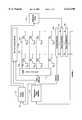
- FIG. 1shows a typical configuration for an integrated circuit including a flash EEPROM memory array 100 and circuitry enabling programming, erasing, reading, and overerase correction of the memory cells in the array 100.
- the flash EEPROM array 100is composed of multiple individual cells, such as cell 102. Each cell has a drain connected to a bitline, such as bitline 104, each bitline being connected to a bitline pull-up circuit 106 and column decoder 108.
- the source of each cellis connected to a common terminal, V SS .
- the control gate of each cellis connected to a wordline, such as wordline 109, that is connected to a row decoder 110.
- the row decoder 110receives voltage signals from a power supply 112 and distributes the particular voltage signals to the wordlines as controlled by a row address received from a processor or state machine 114.
- the bitline pull-up circuit 106receives voltage signals from the power supply 112 and distributes the particular voltage signals to the bitlines as controlled by a signal from the processor 114. Voltages provided by the power supply 112 are controlled by signals received from processor 114.
- the column decoder 108provides signals from particular bitlines to sense amplifiers or comparators 116 as controlled by a column address signal received from processor 114.
- the sense amplifiers 116further receive signals from reference cells of reference array 118.
- An example of circuitry for reference array 118, as well as operation of such circuitryis provided in U.S. Pat. No. 5,828,601, entitled “Programmed Reference,” and U.S. Pat. No. 5,335,198 entitled “Flash EEPROM Array With High Endurance,” both of which are incorporated herein by reference.
- the sense amplifiers 116With signals from the column decoder 108 and reference array 118, the sense amplifiers 116 provide a signal indicating a state of a bitline relative to a reference cell line to which it is connected through data latches or buffers 120 to processor 114.
- high gate and drain voltage pulsesare provided to the cell from power supply 112 while the source of the cell is grounded. For instance, during programming multiple gate voltage pulses of typically 10 volts are each applied for approximately two to three microseconds to a cell, while the drain voltage of the cell is set typically to 5.5 volts and the source of the cell is grounded.
- the large gate and drain voltage pulsesenable electrons flowing from the source to drain to overcome an energy barrier to become "hot electrons" that are able to cross a thin dielectric layer onto the floating gate of the cell.
- This programming proceduretermed "hot electron injection” results in an increase of the threshold voltage for the cell, the threshold voltage being the gate-to-source voltage required for the cell to conduct.
- Fowler-Nordheim tunnelingTo erase a cell in the flash memory array 100, a procedure known as Fowler-Nordheim tunneling is utilized wherein relatively high negative gate-to-source voltage pulses are applied to the cell for a few tenths of a second each. For instance, during erase multiple voltage pulses of minus 10 volts are applied to the control gate of the cell, the drain of the cell is floated and the source of the cell is set to a voltage of less than 6 volts.
- the large negative gate-to-source voltage pulsesenable electrons to tunnel from the floating gate of a cell thereby reducing the cell's threshold voltage.
- the floating gate of a cellis programmed or erased as described above.
- the threshold voltage of a cellis typically set at a voltage of greater than 5 volts, while the threshold voltage of a cell in an erased state is typically limited to a voltage below 3.0 volts.
- a voltage in the range of 3.0 to 6 volts, typically 5 voltsis applied to the control gate.
- the 5 volt read pulseis applied to the gate of an array cell as well as to a cell in the reference array 118 having a threshold voltage of 5 volts.
- a programming state with an array cell in array 100 having a threshold voltage above 5 voltscurrent provided by the reference cell with a threshold voltage of 5 volts will be greater thereby indicating a programmed cell.
- an erased state with a threshold voltage of a cell in array 100 below 3.0 voltscurrent provided by the array cell will be greater than the reference cell with a threshold voltage of 3 volts indicating an erased cell.
- a read voltageis similarly applied to both a cell in the array and to a cell in the reference array 118.
- a reference cell having a threshold of 5 voltsis used for a comparison
- a reference cell having a threshold voltage of 3.0 voltsis used for comparison.
- a typical flash memory arrayall cells are erased simultaneously. Erasing of the memory cells is typically done by repeated applications of the short erase pulses as described above which are applied to each of the cells in an array, such as the flash memory array 100. After each erase pulse, erase verify is performed cell by cell to determine if each cell in the array has a threshold voltage above a limit, such as 3.0 volts. This limit is called "V t ,max" and a cell that has a threshold voltage above V t ,max is "undererased.” If an undererased cell is detected, an additional erase pulse is applied to the entire array.
- V t ,mina threshold voltage below a minimum voltage
- Overerased conditionis undesirable because the programming characteristics of an overerased cell tend to deteriorate more rapidly, which reduces the number of times the cell can be programmed. The number of times that a cell can be programmed is referred to as the endurance of the cell.
- Overerased cellsare also undesirable because they create bitline leakage current during program or read of the cell. For instance, during program or read, only one wordline carries a positive voltage, while the remaining wordlines are typically grounded. With wordlines grounded, or at 0 volts, a cell with a threshold voltage below V t ,min will conduct a small but finite bitline leakage current. With substantial bitline leakage current, power supplies providing power to a bitline during programming may become overloaded. Similarly, with bitline leakage current during read, read errors may occur.
- FIG. 5illustrates the undesirable effect of bitline leakage current during programming.
- FIG. 5is a simplified electrical schematic diagram of a column 500 of flash EEPROM cells 502, 504, 506, and 508.
- the source of each cell in the column 500 of cellsis connected to a common source supply voltage V S .
- a programming voltageis applied to the control gate of the cell 504, which turns it on.
- a current I 2flows through the cell 504 from ground through the source of the cell, the channel (not shown) of the cell and the drain of the cell into the bitline BL.
- the bitline current I BLis equal to I 2 .
- the unselected cells, 502, 506 or 508as illustrated in FIG.
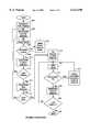
- FIG. 2is a flowchart illustrating a prior art erase and overerase correction procedure. In the procedure, erase is performed first, and then overerase correction is provided. The procedure of FIG. 2 will be described in more detail below.
- steps 202 and 204the row address and column address provided by processor 114 (FIG. 1) are set to an initial address.
- steps 206 and 208an erase verify pulse is provided to a cell as selected by the row and column addresses.
- Outputs from sense amplifiers 116 (FIG. 1)are then utilized by processor 114 (FIG. 1) to determine if the cell referenced by the row and column addresses is undererased. If the cell is undererased, an erase pulse is applied in step 209 to the entire array and the erase verify steps 206 and 208 are repeated.
- step 210If the cell referred to by the row and column addresses is determined to not be undererased in steps 206 and 208, the column address is incremented in step 210. Next, in step 212, if the last column address has not been exceeded, control returns to step 206. Otherwise, in step 214 the row address is incremented, and if the last row address has not been exceeded in step 216, control is returned to step 204. If the last row has been exceeded, the column address is reset in step 218 to begin the overerase correction procedure.
- step 220power supply 112 (FIG. 1) is controlled to provide an overerase verify pulse to the bitline of the cells referred to by the column address, while wordlines remain grounded.
- Outputs from sense amplifiers 116 (FIG. 1)are then provided to the processor 114 (FIG. 1) to determine if the bitline referenced by the column address is providing a leakage current. If the bitline is providing a leakage current, one or more overerased cells exist, so in step 223 power supply 112 is controlled to provide an overerase correction pulse to all of the cells connected to the bitline referred to by the column address and step 220 is then repeated.
- the overerase correction pulse applied in step 223is a relatively high voltage applied to the drain of a cell, such as 6 volts, while its gate and source are typically grounded.
- U.S. Pat. No. 5,359,558 entitled “Flash EEPROM Array With Improved High Endurance,” incorporated herein by referencediscloses further details regarding application of overerase correction pulses.
- step 222If no bitline leakage current is identified in step 222, the column address is incremented in step 224. Next, in step 226, if the last column address has not been exceeded, control is returned to step 220. Otherwise, the overerase correction procedure is complete as indicated at 228.
- overerased cellsmay have been present during erase verify in step 206, undererased, or programmed cells may still be present after the erase procedure is complete.
- one cell in an arraymay erase on the order of 100 times faster than other cells. If the cell verified in step 206 is erased very slowly, while a cell in the same column is erased rapidly by continual applications of the erase pulse of step 209, the cell in the same column that erases faster may become overerased before the cell addressed in step 206 is verified as properly erased. Since during verify in step 206, the remaining cells on the column other than the cell addressed have grounded wordlines, the overerased cell will conduct a bitline leakage current.
- bitline leakage currentadding to the current conducted by the addressed cell, a sense amplifier comparing the current of the addressed cell to current of a reference cell in reference array 118 will prematurely indicate for step 206 that the addressed cell has been properly erased. Thus, after completion of erase, cells may remain undererased.
- FIG. 3is a flowchart illustrating another prior art erase and overerase correction procedure. In the procedure, overerase correction is applied after application of each erase pulse. The procedure of FIG. 3 will be described in more detail below.
- steps 302 and 304the row address and column address provided by the processor 114 (FIG. 1) are set to an initial address.
- steps 306 and 308an erase verify pulse is provided to a cell as selected by the row and column addresses.
- Outputs from sense amplifiers 116 (FIG. 1)are then utilized by processor 114 (FIG. 1) to determine if the cell referenced by the row and column addresses is undererased. If the cell is undererased, an erase pulse is applied to the array in step 309.
- step 309returns to erase verify in step 306
- the column address provided by processor 114(FIG. 1) is reset to an initial address in step 310 to begin an overerase correction procedure.
- step 312 and 314power supply 112 (FIG. 1) is controlled to provide an overerase verify pulse to the bitline of the cells referred by the column address, while wordlines remain grounded.
- Outputs from sense amplifiers 116 (FIG. 1)are then provided to the processor 114 (FIG. 1) to determine if there is a cell on the bitline referenced by the column address that is overerased and providing a leakage current. If there is an overerased cell on the bitline, an overerase correction pulse is applied to all the cells connected to the bitline and steps 312 and 314 are repeated.
- step 312If no overerased cells are identified in steps 312 and 314, the column address is incremented in step 316. Next, in step 318, if the last column address has not been exceeded, control is returned to step 312. Otherwise, control is returned from step 318 to 304 to return to the erase procedure.
- step 306the column address is incremented in step 320.
- step 322if the last column address has not been exceeded, control returns to step 306. Otherwise, in step 324 the row address is incremented, and if the last row address has not been exceeded in step 326, control is returned to step 306. If the last column and row have been exceeded, the combined erase and overerase procedure is complete as indicated at 328.
- the overerase correction procedure after each erase pulse as shown in FIG. 3By applying the overerase correction procedure after each erase pulse as shown in FIG. 3, the extent to which cells are overerased will be reduced relative to the method described in FIG. 2 improving the endurance of cells in the array. Further because overerased cells are removed after each erase pulse, bitline leakage current will not be present during erase verify, thus preventing undererased cells from existing upon completion of the erase procedure.
- bit-by-bit erase verifyingbit-by-bit overerase verifying
- bit-by-bit erase verifyinga second time an array of flash memory cells.
- the threshold voltage of each of the memory cellsis compared to a threshold voltage of a reference cell and an overerase correction pulse is applied to the column in which the overerased cell is located.
- the described methodthus provides a method of erase verifying and overerase verifying an array of memory cells that allows an accurate determination of which cells are overerased further allowing the overerased cells to be reliably overerase corrected.
- FIG. 1shows a typical configuration of an integrated circuit including a flash EEPROM memory array and circuitry enabling programming, erasing, erase verify, reading, overerase correction, and overerase verify in the array;
- FIG. 2is a flowchart of an erase and overerase correction method as known in the prior art
- FIG. 3is a flowchart of a second erase and overerase correction method as known in the prior art
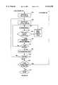
- FIGS. 4A-4Cshow a flowchart of an erase and overerase correction method in accordance with the present invention
- FIG. 5is a schematic of a column of memory cells showing leakage current from cells not being programmed during a programming procedure
- FIG. 6is a schematic of a column of memory cells showing leakage current from cells during the application of an overerase verify pulse during a prior art method
- FIG. 7is a schematic of a column of memory cells during the application of an overerase verify pulse in accordance with the present invention.
- FIG. 8is a graph of a threshold volt age distribution for a flash memory device.
- FIGS. 4A through 4Cshow a flow chart of an erase and overerase correction method in accordance with the present invention.
- the method of the present inventionis an erase procedure followed by an overerase correction procedure with a second erase procedure.
- the overerase correction procedurechecks each bit, bit-by-bit, in the memory array for overerasure.
- steps 402 and 404the row address and column address provided by processor 114 (FIG. 1) are set to an initial address.
- steps 406 and 408an erase verify pulse is provided to a cell as selected by the row and column addresses.
- Outputs from sense amplifies 116 (FIG. 1)are then utilized by processor 114 (FIG. 1) to determine if the threshold voltage V t of the cell referenced by the row and column addresses is greater than V t ,max, that is, to determine if the cell is undererased. If the cell is undererased an erase pulse is applied in step 409 to the entire array and the erase verify steps 406 and 408 are repeated.
- step 412if the last column address has not been exceeded, control returns to step 406. Otherwise, in step 414 the row address is incremented, and if the last row address has not been exceeded in step 416, control is returned to step 406. If the last row has been exceeded, the overerase correction procedure is initiated.
- the overerase correction procedureis shown in FIG. 4B.
- steps 418 and 420the row address and column address provided by processor 114 (FIG. 1) are set to an initial address.
- power supply 112(FIG. 1) is controlled to provide an overerase verify pulse to the bitline referred to by the column address.
- the row decoder 110(FIG. 1) provides a gate voltage to the wordline referred to by the row address and grounds the unselected wordlines.
- the reference array 118 cell (APD ERASE V t cell) used for overerase correctionis set at a given minimum threshold voltage, V t ,min, to provide a given value of reference current.
- the gate voltage of the bit being verifiedis set high enough to far exceed the current contribution of the unselected bits on the column.
- the benefit of thisis that a large differential in current between the selected bit and the unselected bits on the bitline allows a reliable determination of the threshold voltage, V t , of the cell being verified. If it is determined at 424 that the threshold voltage, V t , of the bit being verified is below the minimum threshold voltage, V t ,min, an overerase correction pulse is applied at 426 to the bitline referred to by the column address. If it is determined at 424 that the threshold voltage, V t , of the bit being verified is still below the minimum threshold voltage, V t ,min, another overerase correction pulse is applied at 426. This procedure is repeated until it is determined at 424 that the threshold voltage, V t , of the bit being verified is above the minimum threshold voltage V t ,min, at which point the column address is incremented at 428.
- step 430if the last column address has not been exceeded, control returns to step 422. Otherwise, in step 432 the row address is incremented, and if the last row address has not been exceeded in step 434, control is returned to step 420. If the last row has been exceeded, the next erase verify procedure is initiated.
- the next erase verify procedureis shown in FIG. 4C.
- steps 436 and 438the row address and column address provided by processor 114 (FIG. 1) are set to an initial address.
- steps 440 and 442an erase verify pulse is provided to a cell as selected by the row and column addresses.
- Outputs from sense amplifies 116 (FIG. 1)are then utilized by processor 114 (FIG. 1) to determine if the cell referenced by the row and column addresses is undererased, that is, to determine of the threshold voltage, V t , of the cell is above V t ,max. If the cell is undererased an erase pulse is applied in step 443 to the entire array and the erase verify steps 440 and 442 are repeated.
- step 446if the last column address has not been exceeded, control returns to step 440. Otherwise, in step 448 the row address is incremented, and if the last row address has not been exceeded in step 450, control is returned to step 438. If the last row has been exceeded, it is determined at 452 if there were undererased bits determined at step 442 which necessitated the application of an erase pulse or erase pulses at step 443. If there has been the application of erase pulses at step 443 there may be memory cells that are now overerased and it is necessary to perform an overerase verify procedure.
- step 418(FIG. 4B) and an overerase verify procedure is conducted.
- overerase correctionis needed. If it is determined at step 452 that there were no erase pulses applied in step 443, the process is done as indicated at 454. It is contemplated that in most cases only one erase and overerase cycle will be needed.
- FIG. 6shows how the overerase verify pulse is affected by leakage current during a prior art procedure.
- FIG. 6shows a column of memory cells 600 that is being overerase verified.
- the column of memory cellsincludes cells 602, 604, 606 and 608 and as discussed above, in prior art overerase verify methods, the column is selected and all the wordlines are set to a low voltage typically less than 1 volt as shown at 610.
- the amount of current drawn during the overerase verify procedureis compared to a reference current from the reference array 118 (FIG. 1).
- V tthreshold voltage
- FIG. 7shows how the overerase verify method of the present invention isolates the current from a targeted cell during the overerase verify procedure so that it can be individually compared to a reference current from the reference array 118 (FIG. 1).
- FIG. 7shows a column of memory cells 700 that includes the cell being overerase verified.
- the column of memory cellsincludes cells 702, 704, 706 and 708.
- a specific rowwordline
- the wordlineapplies an overerase verify voltage of ⁇ 5 volts to the control gate of memory cell 704.
- the wordlines for the unselected rowsare grounded.
- the voltages selected during the overerase verify procedureare such that the only current on the bitline BL is the current I 2 from the memory cell 704 if it is overerased. This allows for an accurate and reliable determination of the threshold voltage, V t , of the cell being verified.
- FIG. 8illustrates how the threshold voltages of the cells or bits in a flash EEPROM can differ following an erase operation.
- Curve 800represents the number of cells having particular values of threshold voltage V T . It will be seen that the least erased cells will have relatively high threshold voltages in the region of V t ,max, whereas the most erased cells will have low threshold voltages in the region of V t ,min that can be below V t ,min as indicated by the dashed line 802.
- the characteristic curve illustrated in FIG. 8is known as the threshold voltage distribution.
- the overerase correction procedureis designed to increase the threshold voltage of overerased cells from the area defined by the dashed line 802 to within the curve 800 without affecting (increasing) the threshold voltage of the least erased cells in the region of V t ,max.
- the described methodthus provides an accurate and reliable method of erase verifying and overerase verifying an array of memory cells.
Landscapes
- Read Only Memory (AREA)
Abstract
Description
Claims (6)
Priority Applications (1)
| Application Number | Priority Date | Filing Date | Title |
|---|---|---|---|
| US09/413,182US6122198A (en) | 1999-08-13 | 1999-10-05 | Bit by bit APDE verify for flash memory applications |
Applications Claiming Priority (2)
| Application Number | Priority Date | Filing Date | Title |
|---|---|---|---|
| US14878299P | 1999-08-13 | 1999-08-13 | |
| US09/413,182US6122198A (en) | 1999-08-13 | 1999-10-05 | Bit by bit APDE verify for flash memory applications |
Publications (1)
| Publication Number | Publication Date |
|---|---|
| US6122198Atrue US6122198A (en) | 2000-09-19 |
Family
ID=26846161
Family Applications (1)
| Application Number | Title | Priority Date | Filing Date |
|---|---|---|---|
| US09/413,182Expired - LifetimeUS6122198A (en) | 1999-08-13 | 1999-10-05 | Bit by bit APDE verify for flash memory applications |
Country Status (1)
| Country | Link |
|---|---|
| US (1) | US6122198A (en) |
Cited By (46)
| Publication number | Priority date | Publication date | Assignee | Title |
|---|---|---|---|---|
| US6452840B1 (en)* | 2000-10-21 | 2002-09-17 | Advanced Micro Devices, Inc. | Feedback method to optimize electric field during channel erase of flash memory devices |
| US6493280B2 (en)* | 2001-03-05 | 2002-12-10 | Micron Technology, Inc. | Method of reducing trapped holes induced by erase operations in the tunnel oxide of flash memory cells |
| US6498752B1 (en) | 2001-08-27 | 2002-12-24 | Aplus Flash Technology, Inc. | Three step write process used for a nonvolatile NOR type EEPROM memory |
| US6515910B1 (en) | 2001-03-06 | 2003-02-04 | Aplus Flash Technology Inc. | Bit-by-bit Vt-correction operation for nonvolatile semiconductor one-transistor cell, nor-type flash EEPROM |
| US6515908B2 (en)* | 2000-11-16 | 2003-02-04 | Mitsubishi Denki Kabushiki Kaisha | Nonvolatile semiconductor memory device having reduced erase time and method of erasing data of the same |
| US20030067818A1 (en)* | 2001-09-12 | 2003-04-10 | Sharp Kabushiki Kaisha | Nonvolatile semiconductor memory device and method of detecting overerased cell |
| WO2003067597A3 (en)* | 2002-02-06 | 2003-11-13 | Sandisk Corp | Implementation of an inhibit during soft programming to tighten an erase voltage distribution |
| US6711062B1 (en) | 2002-07-17 | 2004-03-23 | Taiwan Semiconductor Manufacturing Company | Erase method of split gate flash memory reference cells |
| US20040109379A1 (en)* | 2002-01-25 | 2004-06-10 | Yue-Der Chih | Method of marginal erasure for the testing of flash memories |
| US20050144553A1 (en)* | 2000-04-06 | 2005-06-30 | International Business Machines Corporation | Longest prefix match (LPM) algorithm implementation for a network processor |
| EP1306855A3 (en)* | 2001-10-24 | 2006-05-24 | Saifun Semiconductors Ltd. | Method for erasing a memory cell |
| US20060126383A1 (en)* | 2004-12-09 | 2006-06-15 | Saifun Semiconductors, Ltd. | Method for reading non-volatile memory cells |
| US20070058444A1 (en)* | 2005-09-06 | 2007-03-15 | Saifun Semiconductors, Ltd. | Method and circuit for erasing a non-volatile memory cell |
| US7221138B2 (en) | 2005-09-27 | 2007-05-22 | Saifun Semiconductors Ltd | Method and apparatus for measuring charge pump output current |
| US7317633B2 (en) | 2004-07-06 | 2008-01-08 | Saifun Semiconductors Ltd | Protection of NROM devices from charge damage |
| US7352627B2 (en) | 2006-01-03 | 2008-04-01 | Saifon Semiconductors Ltd. | Method, system, and circuit for operating a non-volatile memory array |
| US20080084737A1 (en)* | 2006-06-30 | 2008-04-10 | Eon Silicon Solutions, Inc. Usa | Method of achieving zero column leakage after erase in flash EPROM |
| US20080089132A1 (en)* | 2006-10-13 | 2008-04-17 | Fumitoshi Ito | Partitioned soft programming in non-volatile memory |
| US20080089133A1 (en)* | 2006-10-13 | 2008-04-17 | Fumitoshi Ito | Systems for partitioned soft programming in non-volatile memory |
| US20080089135A1 (en)* | 2006-10-13 | 2008-04-17 | Fumitoshi Ito | Systems for partitioned erase and erase verification in non-volatile memory |
| US7369440B2 (en) | 2005-01-19 | 2008-05-06 | Saifun Semiconductors Ltd. | Method, circuit and systems for erasing one or more non-volatile memory cells |
| US20080117688A1 (en)* | 2006-11-22 | 2008-05-22 | Samsung Electronics Co., Ltd. | Flash Memory Devices that Utilize Age-Based Verify Voltages to Increase Data Reliability and Methods of Operating Same |
| US7405969B2 (en) | 1997-08-01 | 2008-07-29 | Saifun Semiconductors Ltd. | Non-volatile memory cell and non-volatile memory devices |
| US7420848B2 (en) | 2002-01-31 | 2008-09-02 | Saifun Semiconductors Ltd. | Method, system, and circuit for operating a non-volatile memory array |
| US7457183B2 (en) | 2003-09-16 | 2008-11-25 | Saifun Semiconductors Ltd. | Operating array cells with matched reference cells |
| US7466594B2 (en) | 2004-08-12 | 2008-12-16 | Saifun Semiconductors Ltd. | Dynamic matching of signal path and reference path for sensing |
| US7512009B2 (en) | 2001-04-05 | 2009-03-31 | Saifun Semiconductors Ltd. | Method for programming a reference cell |
| US7532529B2 (en) | 2004-03-29 | 2009-05-12 | Saifun Semiconductors Ltd. | Apparatus and methods for multi-level sensing in a memory array |
| US7535765B2 (en) | 2004-12-09 | 2009-05-19 | Saifun Semiconductors Ltd. | Non-volatile memory device and method for reading cells |
| US7605579B2 (en) | 2006-09-18 | 2009-10-20 | Saifun Semiconductors Ltd. | Measuring and controlling current consumption and output current of charge pumps |
| US7638850B2 (en) | 2004-10-14 | 2009-12-29 | Saifun Semiconductors Ltd. | Non-volatile memory structure and method of fabrication |
| US7638835B2 (en) | 2006-02-28 | 2009-12-29 | Saifun Semiconductors Ltd. | Double density NROM with nitride strips (DDNS) |
| US7668017B2 (en) | 2005-08-17 | 2010-02-23 | Saifun Semiconductors Ltd. | Method of erasing non-volatile memory cells |
| US7675782B2 (en) | 2002-10-29 | 2010-03-09 | Saifun Semiconductors Ltd. | Method, system and circuit for programming a non-volatile memory array |
| US7692961B2 (en) | 2006-02-21 | 2010-04-06 | Saifun Semiconductors Ltd. | Method, circuit and device for disturb-control of programming nonvolatile memory cells by hot-hole injection (HHI) and by channel hot-electron (CHE) injection |
| US7701779B2 (en) | 2006-04-27 | 2010-04-20 | Sajfun Semiconductors Ltd. | Method for programming a reference cell |
| US7738304B2 (en) | 2002-07-10 | 2010-06-15 | Saifun Semiconductors Ltd. | Multiple use memory chip |
| US7743230B2 (en) | 2003-01-31 | 2010-06-22 | Saifun Semiconductors Ltd. | Memory array programming circuit and a method for using the circuit |
| US7760554B2 (en) | 2006-02-21 | 2010-07-20 | Saifun Semiconductors Ltd. | NROM non-volatile memory and mode of operation |
| US7768826B2 (en) | 2006-10-13 | 2010-08-03 | Sandisk Corporation | Methods for partitioned erase and erase verification in non-volatile memory to compensate for capacitive coupling effects |
| US7786512B2 (en) | 2005-07-18 | 2010-08-31 | Saifun Semiconductors Ltd. | Dense non-volatile memory array and method of fabrication |
| US7808818B2 (en) | 2006-01-12 | 2010-10-05 | Saifun Semiconductors Ltd. | Secondary injection for NROM |
| US8053812B2 (en) | 2005-03-17 | 2011-11-08 | Spansion Israel Ltd | Contact in planar NROM technology |
| CN102568588A (en)* | 2010-12-31 | 2012-07-11 | 北京兆易创新科技有限公司 | Over-erasing checking method and over-erasing checking system for non-volatile memory |
| US8253452B2 (en) | 2006-02-21 | 2012-08-28 | Spansion Israel Ltd | Circuit and method for powering up an integrated circuit and an integrated circuit utilizing same |
| CN103035295A (en)* | 2011-09-29 | 2013-04-10 | 赛普拉斯半导体公司 | IT smart write |
Citations (4)
| Publication number | Priority date | Publication date | Assignee | Title |
|---|---|---|---|---|
| US5237535A (en)* | 1991-10-09 | 1993-08-17 | Intel Corporation | Method of repairing overerased cells in a flash memory |
| US5642311A (en)* | 1995-10-24 | 1997-06-24 | Advanced Micro Devices | Overerase correction for flash memory which limits overerase and prevents erase verify errors |
| US5732019A (en)* | 1994-09-30 | 1998-03-24 | Nec Corporation | Initialization of electrically erasable non-volatile semiconductor memory device |
| US5901090A (en)* | 1998-05-27 | 1999-05-04 | Advanced Micro Devices | Method for erasing flash electrically erasable programmable read-only memory (EEPROM) |
- 1999
- 1999-10-05USUS09/413,182patent/US6122198A/ennot_activeExpired - Lifetime
Patent Citations (4)
| Publication number | Priority date | Publication date | Assignee | Title |
|---|---|---|---|---|
| US5237535A (en)* | 1991-10-09 | 1993-08-17 | Intel Corporation | Method of repairing overerased cells in a flash memory |
| US5732019A (en)* | 1994-09-30 | 1998-03-24 | Nec Corporation | Initialization of electrically erasable non-volatile semiconductor memory device |
| US5642311A (en)* | 1995-10-24 | 1997-06-24 | Advanced Micro Devices | Overerase correction for flash memory which limits overerase and prevents erase verify errors |
| US5901090A (en)* | 1998-05-27 | 1999-05-04 | Advanced Micro Devices | Method for erasing flash electrically erasable programmable read-only memory (EEPROM) |
Cited By (62)
| Publication number | Priority date | Publication date | Assignee | Title |
|---|---|---|---|---|
| US7405969B2 (en) | 1997-08-01 | 2008-07-29 | Saifun Semiconductors Ltd. | Non-volatile memory cell and non-volatile memory devices |
| US20050144553A1 (en)* | 2000-04-06 | 2005-06-30 | International Business Machines Corporation | Longest prefix match (LPM) algorithm implementation for a network processor |
| US6452840B1 (en)* | 2000-10-21 | 2002-09-17 | Advanced Micro Devices, Inc. | Feedback method to optimize electric field during channel erase of flash memory devices |
| US6515908B2 (en)* | 2000-11-16 | 2003-02-04 | Mitsubishi Denki Kabushiki Kaisha | Nonvolatile semiconductor memory device having reduced erase time and method of erasing data of the same |
| US6493280B2 (en)* | 2001-03-05 | 2002-12-10 | Micron Technology, Inc. | Method of reducing trapped holes induced by erase operations in the tunnel oxide of flash memory cells |
| US6515910B1 (en) | 2001-03-06 | 2003-02-04 | Aplus Flash Technology Inc. | Bit-by-bit Vt-correction operation for nonvolatile semiconductor one-transistor cell, nor-type flash EEPROM |
| US7512009B2 (en) | 2001-04-05 | 2009-03-31 | Saifun Semiconductors Ltd. | Method for programming a reference cell |
| US6498752B1 (en) | 2001-08-27 | 2002-12-24 | Aplus Flash Technology, Inc. | Three step write process used for a nonvolatile NOR type EEPROM memory |
| US20030067818A1 (en)* | 2001-09-12 | 2003-04-10 | Sharp Kabushiki Kaisha | Nonvolatile semiconductor memory device and method of detecting overerased cell |
| US6714459B2 (en)* | 2001-09-12 | 2004-03-30 | Sharp Kabushiki Kaisha | Nonvolatile semiconductor memory device and method of detecting overerased cell |
| EP1306855A3 (en)* | 2001-10-24 | 2006-05-24 | Saifun Semiconductors Ltd. | Method for erasing a memory cell |
| US6842381B2 (en) | 2002-01-25 | 2005-01-11 | Taiwan Semiconductor Manufacturing Co. | Method of marginal erasure for the testing of flash memories |
| US20040109379A1 (en)* | 2002-01-25 | 2004-06-10 | Yue-Der Chih | Method of marginal erasure for the testing of flash memories |
| US7420848B2 (en) | 2002-01-31 | 2008-09-02 | Saifun Semiconductors Ltd. | Method, system, and circuit for operating a non-volatile memory array |
| US6661711B2 (en) | 2002-02-06 | 2003-12-09 | Sandisk Corporation | Implementation of an inhibit during soft programming to tighten an erase voltage distribution |
| WO2003067597A3 (en)* | 2002-02-06 | 2003-11-13 | Sandisk Corp | Implementation of an inhibit during soft programming to tighten an erase voltage distribution |
| US7738304B2 (en) | 2002-07-10 | 2010-06-15 | Saifun Semiconductors Ltd. | Multiple use memory chip |
| US20040145948A1 (en)* | 2002-07-17 | 2004-07-29 | Taiwan Semiconductor Manufacturing Company | Power-on reset circuit for erasing of split gate flash memory reference cells |
| US6954379B2 (en) | 2002-07-17 | 2005-10-11 | Taiwan Semiconductor Manufacturing Company | Power-on reset circuit for erasing of split gate flash memory reference cells |
| US6711062B1 (en) | 2002-07-17 | 2004-03-23 | Taiwan Semiconductor Manufacturing Company | Erase method of split gate flash memory reference cells |
| US7675782B2 (en) | 2002-10-29 | 2010-03-09 | Saifun Semiconductors Ltd. | Method, system and circuit for programming a non-volatile memory array |
| US7743230B2 (en) | 2003-01-31 | 2010-06-22 | Saifun Semiconductors Ltd. | Memory array programming circuit and a method for using the circuit |
| US7457183B2 (en) | 2003-09-16 | 2008-11-25 | Saifun Semiconductors Ltd. | Operating array cells with matched reference cells |
| US7532529B2 (en) | 2004-03-29 | 2009-05-12 | Saifun Semiconductors Ltd. | Apparatus and methods for multi-level sensing in a memory array |
| US7317633B2 (en) | 2004-07-06 | 2008-01-08 | Saifun Semiconductors Ltd | Protection of NROM devices from charge damage |
| US7466594B2 (en) | 2004-08-12 | 2008-12-16 | Saifun Semiconductors Ltd. | Dynamic matching of signal path and reference path for sensing |
| US7964459B2 (en) | 2004-10-14 | 2011-06-21 | Spansion Israel Ltd. | Non-volatile memory structure and method of fabrication |
| US7638850B2 (en) | 2004-10-14 | 2009-12-29 | Saifun Semiconductors Ltd. | Non-volatile memory structure and method of fabrication |
| US7242618B2 (en) | 2004-12-09 | 2007-07-10 | Saifun Semiconductors Ltd. | Method for reading non-volatile memory cells |
| US7535765B2 (en) | 2004-12-09 | 2009-05-19 | Saifun Semiconductors Ltd. | Non-volatile memory device and method for reading cells |
| US20060126383A1 (en)* | 2004-12-09 | 2006-06-15 | Saifun Semiconductors, Ltd. | Method for reading non-volatile memory cells |
| US7369440B2 (en) | 2005-01-19 | 2008-05-06 | Saifun Semiconductors Ltd. | Method, circuit and systems for erasing one or more non-volatile memory cells |
| US7468926B2 (en) | 2005-01-19 | 2008-12-23 | Saifun Semiconductors Ltd. | Partial erase verify |
| US8053812B2 (en) | 2005-03-17 | 2011-11-08 | Spansion Israel Ltd | Contact in planar NROM technology |
| US7786512B2 (en) | 2005-07-18 | 2010-08-31 | Saifun Semiconductors Ltd. | Dense non-volatile memory array and method of fabrication |
| US7668017B2 (en) | 2005-08-17 | 2010-02-23 | Saifun Semiconductors Ltd. | Method of erasing non-volatile memory cells |
| US8116142B2 (en) | 2005-09-06 | 2012-02-14 | Infineon Technologies Ag | Method and circuit for erasing a non-volatile memory cell |
| US20070058444A1 (en)* | 2005-09-06 | 2007-03-15 | Saifun Semiconductors, Ltd. | Method and circuit for erasing a non-volatile memory cell |
| US7221138B2 (en) | 2005-09-27 | 2007-05-22 | Saifun Semiconductors Ltd | Method and apparatus for measuring charge pump output current |
| US7352627B2 (en) | 2006-01-03 | 2008-04-01 | Saifon Semiconductors Ltd. | Method, system, and circuit for operating a non-volatile memory array |
| US7808818B2 (en) | 2006-01-12 | 2010-10-05 | Saifun Semiconductors Ltd. | Secondary injection for NROM |
| US7760554B2 (en) | 2006-02-21 | 2010-07-20 | Saifun Semiconductors Ltd. | NROM non-volatile memory and mode of operation |
| US7692961B2 (en) | 2006-02-21 | 2010-04-06 | Saifun Semiconductors Ltd. | Method, circuit and device for disturb-control of programming nonvolatile memory cells by hot-hole injection (HHI) and by channel hot-electron (CHE) injection |
| US8253452B2 (en) | 2006-02-21 | 2012-08-28 | Spansion Israel Ltd | Circuit and method for powering up an integrated circuit and an integrated circuit utilizing same |
| US7638835B2 (en) | 2006-02-28 | 2009-12-29 | Saifun Semiconductors Ltd. | Double density NROM with nitride strips (DDNS) |
| US7701779B2 (en) | 2006-04-27 | 2010-04-20 | Sajfun Semiconductors Ltd. | Method for programming a reference cell |
| US20080084737A1 (en)* | 2006-06-30 | 2008-04-10 | Eon Silicon Solutions, Inc. Usa | Method of achieving zero column leakage after erase in flash EPROM |
| US7605579B2 (en) | 2006-09-18 | 2009-10-20 | Saifun Semiconductors Ltd. | Measuring and controlling current consumption and output current of charge pumps |
| US7535766B2 (en) | 2006-10-13 | 2009-05-19 | Sandisk Corporation | Systems for partitioned soft programming in non-volatile memory |
| US20080089133A1 (en)* | 2006-10-13 | 2008-04-17 | Fumitoshi Ito | Systems for partitioned soft programming in non-volatile memory |
| US7768826B2 (en) | 2006-10-13 | 2010-08-03 | Sandisk Corporation | Methods for partitioned erase and erase verification in non-volatile memory to compensate for capacitive coupling effects |
| US7499317B2 (en)* | 2006-10-13 | 2009-03-03 | Sandisk Corporation | System for partitioned erase and erase verification in a non-volatile memory to compensate for capacitive coupling |
| US7499338B2 (en) | 2006-10-13 | 2009-03-03 | Sandisk Corporation | Partitioned soft programming in non-volatile memory |
| US20080089132A1 (en)* | 2006-10-13 | 2008-04-17 | Fumitoshi Ito | Partitioned soft programming in non-volatile memory |
| US20080089135A1 (en)* | 2006-10-13 | 2008-04-17 | Fumitoshi Ito | Systems for partitioned erase and erase verification in non-volatile memory |
| US20080117688A1 (en)* | 2006-11-22 | 2008-05-22 | Samsung Electronics Co., Ltd. | Flash Memory Devices that Utilize Age-Based Verify Voltages to Increase Data Reliability and Methods of Operating Same |
| US7986560B2 (en) | 2006-11-22 | 2011-07-26 | Samsung Electronics Co., Ltd. | Flash memory devices that utilize age-based verify voltages to increase data reliability and methods of operating same |
| US7692970B2 (en)* | 2006-11-22 | 2010-04-06 | Samsung Electronics Co., Ltd. | Flash memory devices that utilize age-based verify voltages to increase data reliability and methods of operating same |
| CN102568588A (en)* | 2010-12-31 | 2012-07-11 | 北京兆易创新科技有限公司 | Over-erasing checking method and over-erasing checking system for non-volatile memory |
| CN102568588B (en)* | 2010-12-31 | 2016-03-23 | 北京兆易创新科技股份有限公司 | A kind of erasing method of calibration and check system excessively of nonvolatile memory |
| CN103035295A (en)* | 2011-09-29 | 2013-04-10 | 赛普拉斯半导体公司 | IT smart write |
| CN103035295B (en)* | 2011-09-29 | 2021-02-12 | 经度快闪存储解决方案有限责任公司 | Smart write of one transistor |
Similar Documents
| Publication | Publication Date | Title |
|---|---|---|
| US6122198A (en) | Bit by bit APDE verify for flash memory applications | |
| US5642311A (en) | Overerase correction for flash memory which limits overerase and prevents erase verify errors | |
| US6046932A (en) | Circuit implementation to quench bit line leakage current in programming and over-erase correction modes in flash EEPROM | |
| US6252803B1 (en) | Automatic program disturb with intelligent soft programming for flash cells | |
| US6620682B1 (en) | Set of three level concurrent word line bias conditions for a nor type flash memory array | |
| US6498752B1 (en) | Three step write process used for a nonvolatile NOR type EEPROM memory | |
| JP3720859B2 (en) | Semiconductor integrated circuit memory device | |
| US6452837B2 (en) | Nonvolatile semiconductor memory and threshold voltage control method therefor | |
| US20080137436A1 (en) | Programming method for non-volatile memory and non-volatile memory-based programmable logic device | |
| US20020060929A1 (en) | Flash memory device capable of preventing an over-erase of flash memory cells and erase method thereof | |
| US5901090A (en) | Method for erasing flash electrically erasable programmable read-only memory (EEPROM) | |
| US6714459B2 (en) | Nonvolatile semiconductor memory device and method of detecting overerased cell | |
| US6452840B1 (en) | Feedback method to optimize electric field during channel erase of flash memory devices | |
| US6400608B1 (en) | Accurate verify apparatus and method for NOR flash memory cells in the presence of high column leakage | |
| US6285588B1 (en) | Erase scheme to tighten the threshold voltage distribution of EEPROM flash memory cells | |
| US5875130A (en) | Method for programming flash electrically erasable programmable read-only memory | |
| US7190624B2 (en) | Flash memory device capable of preventing an over-erase of flash memory cells and erase method thereof | |
| US7227784B2 (en) | Nonvolatile semiconductor memory device performing erase operation that creates narrow threshold distribution | |
| KR20030019854A (en) | Nonvolatile semiconductor memory device that can suppress effect of threshold voltage variation of memory cell transistor | |
| WO1999033060A1 (en) | Integrated program verify page buffer | |
| US7020021B1 (en) | Ramped soft programming for control of erase voltage distributions in flash memory devices | |
| US6023426A (en) | Method of achieving narrow VT distribution after erase in flash EEPROM | |
| US6198664B1 (en) | APDE scheme for flash memory application | |
| US20080084737A1 (en) | Method of achieving zero column leakage after erase in flash EPROM | |
| US7599228B1 (en) | Flash memory device having increased over-erase correction efficiency and robustness against device variations |
Legal Events
| Date | Code | Title | Description |
|---|---|---|---|
| AS | Assignment | Owner name:ADVANCED MICRO DEVICES, INC., CALIFORNIA Free format text:ASSIGNMENT OF ASSIGNORS INTEREST;ASSIGNORS:HADDAD, SAMEER S.;GUTALA, RAVI P.;BILL, COLIN;REEL/FRAME:010308/0292;SIGNING DATES FROM 19990820 TO 19990924 | |
| STCF | Information on status: patent grant | Free format text:PATENTED CASE | |
| FPAY | Fee payment | Year of fee payment:4 | |
| AS | Assignment | Owner name:SPANSION INC., CALIFORNIA Free format text:ASSIGNMENT OF ASSIGNORS INTEREST;ASSIGNOR:ADVANCED MICRO DEVICES, INC.;REEL/FRAME:019028/0644 Effective date:20070131 | |
| AS | Assignment | Owner name:SPANSION LLC, CALIFORNIA Free format text:ASSIGNMENT OF ASSIGNORS INTEREST;ASSIGNOR:SPANSION INC.;REEL/FRAME:019069/0046 Effective date:20070131 | |
| FPAY | Fee payment | Year of fee payment:8 | |
| AS | Assignment | Owner name:BARCLAYS BANK PLC,NEW YORK Free format text:SECURITY AGREEMENT;ASSIGNORS:SPANSION LLC;SPANSION INC.;SPANSION TECHNOLOGY INC.;AND OTHERS;REEL/FRAME:024522/0338 Effective date:20100510 Owner name:BARCLAYS BANK PLC, NEW YORK Free format text:SECURITY AGREEMENT;ASSIGNORS:SPANSION LLC;SPANSION INC.;SPANSION TECHNOLOGY INC.;AND OTHERS;REEL/FRAME:024522/0338 Effective date:20100510 | |
| FPAY | Fee payment | Year of fee payment:12 | |
| AS | Assignment | Owner name:SPANSION TECHNOLOGY LLC, CALIFORNIA Free format text:RELEASE BY SECURED PARTY;ASSIGNOR:BARCLAYS BANK PLC;REEL/FRAME:035201/0159 Effective date:20150312 Owner name:SPANSION INC., CALIFORNIA Free format text:RELEASE BY SECURED PARTY;ASSIGNOR:BARCLAYS BANK PLC;REEL/FRAME:035201/0159 Effective date:20150312 Owner name:SPANSION LLC, CALIFORNIA Free format text:RELEASE BY SECURED PARTY;ASSIGNOR:BARCLAYS BANK PLC;REEL/FRAME:035201/0159 Effective date:20150312 | |
| AS | Assignment | Owner name:MORGAN STANLEY SENIOR FUNDING, INC., NEW YORK Free format text:SECURITY INTEREST;ASSIGNORS:CYPRESS SEMICONDUCTOR CORPORATION;SPANSION LLC;REEL/FRAME:035240/0429 Effective date:20150312 | |
| AS | Assignment | Owner name:CYPRESS SEMICONDUCTOR CORPORATION, CALIFORNIA Free format text:ASSIGNMENT OF ASSIGNORS INTEREST;ASSIGNOR:SPANSION, LLC;REEL/FRAME:036017/0625 Effective date:20150601 | |
| AS | Assignment | Owner name:SPANSION LLC, CALIFORNIA Free format text:PARTIAL RELEASE OF SECURITY INTEREST IN PATENTS;ASSIGNOR:MORGAN STANLEY SENIOR FUNDING, INC., AS COLLATERAL AGENT;REEL/FRAME:039708/0001 Effective date:20160811 Owner name:CYPRESS SEMICONDUCTOR CORPORATION, CALIFORNIA Free format text:PARTIAL RELEASE OF SECURITY INTEREST IN PATENTS;ASSIGNOR:MORGAN STANLEY SENIOR FUNDING, INC., AS COLLATERAL AGENT;REEL/FRAME:039708/0001 Effective date:20160811 | |
| AS | Assignment | Owner name:MONTEREY RESEARCH, LLC, CALIFORNIA Free format text:ASSIGNMENT OF ASSIGNORS INTEREST;ASSIGNOR:CYPRESS SEMICONDUCTOR CORPORATION;REEL/FRAME:040911/0238 Effective date:20160811 | |
| AS | Assignment | Owner name:MORGAN STANLEY SENIOR FUNDING, INC., NEW YORK Free format text:CORRECTIVE ASSIGNMENT TO CORRECT THE 8647899 PREVIOUSLY RECORDED ON REEL 035240 FRAME 0429. ASSIGNOR(S) HEREBY CONFIRMS THE SECURITY INTERST;ASSIGNORS:CYPRESS SEMICONDUCTOR CORPORATION;SPANSION LLC;REEL/FRAME:058002/0470 Effective date:20150312 |