US6122187A - Stacked integrated circuits - Google Patents
Stacked integrated circuitsDownload PDFInfo
- Publication number
- US6122187A US6122187AUS09/198,554US19855498AUS6122187AUS 6122187 AUS6122187 AUS 6122187AUS 19855498 AUS19855498 AUS 19855498AUS 6122187 AUS6122187 AUS 6122187A
- Authority
- US
- United States
- Prior art keywords
- semiconductor
- memory
- conductor
- microbumps
- conductive layer
- Prior art date
- Legal status (The legal status is an assumption and is not a legal conclusion. Google has not performed a legal analysis and makes no representation as to the accuracy of the status listed.)
- Expired - Lifetime
Links
Images


Classifications
- H—ELECTRICITY
- H01—ELECTRIC ELEMENTS
- H01L—SEMICONDUCTOR DEVICES NOT COVERED BY CLASS H10
- H01L25/00—Assemblies consisting of a plurality of semiconductor or other solid state devices
- H01L25/03—Assemblies consisting of a plurality of semiconductor or other solid state devices all the devices being of a type provided for in a single subclass of subclasses H10B, H10D, H10F, H10H, H10K or H10N, e.g. assemblies of rectifier diodes
- H01L25/04—Assemblies consisting of a plurality of semiconductor or other solid state devices all the devices being of a type provided for in a single subclass of subclasses H10B, H10D, H10F, H10H, H10K or H10N, e.g. assemblies of rectifier diodes the devices not having separate containers
- H01L25/065—Assemblies consisting of a plurality of semiconductor or other solid state devices all the devices being of a type provided for in a single subclass of subclasses H10B, H10D, H10F, H10H, H10K or H10N, e.g. assemblies of rectifier diodes the devices not having separate containers the devices being of a type provided for in group H10D89/00
- H01L25/0657—Stacked arrangements of devices
- G—PHYSICS
- G11—INFORMATION STORAGE
- G11C—STATIC STORES
- G11C5/00—Details of stores covered by group G11C11/00
- G11C5/02—Disposition of storage elements, e.g. in the form of a matrix array
- G11C5/04—Supports for storage elements, e.g. memory modules; Mounting or fixing of storage elements on such supports
- G—PHYSICS
- G11—INFORMATION STORAGE
- G11C—STATIC STORES
- G11C5/00—Details of stores covered by group G11C11/00
- G11C5/06—Arrangements for interconnecting storage elements electrically, e.g. by wiring
- H—ELECTRICITY
- H01—ELECTRIC ELEMENTS
- H01L—SEMICONDUCTOR DEVICES NOT COVERED BY CLASS H10
- H01L23/00—Details of semiconductor or other solid state devices
- H01L23/48—Arrangements for conducting electric current to or from the solid state body in operation, e.g. leads, terminal arrangements ; Selection of materials therefor
- H01L23/481—Internal lead connections, e.g. via connections, feedthrough structures
- H—ELECTRICITY
- H01—ELECTRIC ELEMENTS
- H01L—SEMICONDUCTOR DEVICES NOT COVERED BY CLASS H10
- H01L2223/00—Details relating to semiconductor or other solid state devices covered by the group H01L23/00
- H01L2223/58—Structural electrical arrangements for semiconductor devices not otherwise provided for
- H01L2223/64—Impedance arrangements
- H01L2223/66—High-frequency adaptations
- H01L2223/6605—High-frequency electrical connections
- H01L2223/6616—Vertical connections, e.g. vias
- H01L2223/6622—Coaxial feed-throughs in active or passive substrates
- H—ELECTRICITY
- H01—ELECTRIC ELEMENTS
- H01L—SEMICONDUCTOR DEVICES NOT COVERED BY CLASS H10
- H01L2224/00—Indexing scheme for arrangements for connecting or disconnecting semiconductor or solid-state bodies and methods related thereto as covered by H01L24/00
- H01L2224/01—Means for bonding being attached to, or being formed on, the surface to be connected, e.g. chip-to-package, die-attach, "first-level" interconnects; Manufacturing methods related thereto
- H01L2224/02—Bonding areas; Manufacturing methods related thereto
- H01L2224/04—Structure, shape, material or disposition of the bonding areas prior to the connecting process
- H01L2224/05—Structure, shape, material or disposition of the bonding areas prior to the connecting process of an individual bonding area
- H01L2224/0554—External layer
- H01L2224/0556—Disposition
- H01L2224/05568—Disposition the whole external layer protruding from the surface
- H—ELECTRICITY
- H01—ELECTRIC ELEMENTS
- H01L—SEMICONDUCTOR DEVICES NOT COVERED BY CLASS H10
- H01L2224/00—Indexing scheme for arrangements for connecting or disconnecting semiconductor or solid-state bodies and methods related thereto as covered by H01L24/00
- H01L2224/01—Means for bonding being attached to, or being formed on, the surface to be connected, e.g. chip-to-package, die-attach, "first-level" interconnects; Manufacturing methods related thereto
- H01L2224/02—Bonding areas; Manufacturing methods related thereto
- H01L2224/04—Structure, shape, material or disposition of the bonding areas prior to the connecting process
- H01L2224/05—Structure, shape, material or disposition of the bonding areas prior to the connecting process of an individual bonding area
- H01L2224/0554—External layer
- H01L2224/05573—Single external layer
- H—ELECTRICITY
- H01—ELECTRIC ELEMENTS
- H01L—SEMICONDUCTOR DEVICES NOT COVERED BY CLASS H10
- H01L2224/00—Indexing scheme for arrangements for connecting or disconnecting semiconductor or solid-state bodies and methods related thereto as covered by H01L24/00
- H01L2224/01—Means for bonding being attached to, or being formed on, the surface to be connected, e.g. chip-to-package, die-attach, "first-level" interconnects; Manufacturing methods related thereto
- H01L2224/02—Bonding areas; Manufacturing methods related thereto
- H01L2224/04—Structure, shape, material or disposition of the bonding areas prior to the connecting process
- H01L2224/05—Structure, shape, material or disposition of the bonding areas prior to the connecting process of an individual bonding area
- H01L2224/0554—External layer
- H01L2224/05599—Material
- H01L2224/056—Material with a principal constituent of the material being a metal or a metalloid, e.g. boron [B], silicon [Si], germanium [Ge], arsenic [As], antimony [Sb], tellurium [Te] and polonium [Po], and alloys thereof
- H—ELECTRICITY
- H01—ELECTRIC ELEMENTS
- H01L—SEMICONDUCTOR DEVICES NOT COVERED BY CLASS H10
- H01L2224/00—Indexing scheme for arrangements for connecting or disconnecting semiconductor or solid-state bodies and methods related thereto as covered by H01L24/00
- H01L2224/01—Means for bonding being attached to, or being formed on, the surface to be connected, e.g. chip-to-package, die-attach, "first-level" interconnects; Manufacturing methods related thereto
- H01L2224/10—Bump connectors; Manufacturing methods related thereto
- H01L2224/15—Structure, shape, material or disposition of the bump connectors after the connecting process
- H01L2224/16—Structure, shape, material or disposition of the bump connectors after the connecting process of an individual bump connector
- H—ELECTRICITY
- H01—ELECTRIC ELEMENTS
- H01L—SEMICONDUCTOR DEVICES NOT COVERED BY CLASS H10
- H01L2225/00—Details relating to assemblies covered by the group H01L25/00 but not provided for in its subgroups
- H01L2225/03—All the devices being of a type provided for in the same main group of the same subclass of class H10, e.g. assemblies of rectifier diodes
- H01L2225/04—All the devices being of a type provided for in the same main group of the same subclass of class H10, e.g. assemblies of rectifier diodes the devices not having separate containers
- H01L2225/065—All the devices being of a type provided for in the same main group of the same subclass of class H10
- H01L2225/06503—Stacked arrangements of devices
- H01L2225/0652—Bump or bump-like direct electrical connections from substrate to substrate
- H—ELECTRICITY
- H01—ELECTRIC ELEMENTS
- H01L—SEMICONDUCTOR DEVICES NOT COVERED BY CLASS H10
- H01L2225/00—Details relating to assemblies covered by the group H01L25/00 but not provided for in its subgroups
- H01L2225/03—All the devices being of a type provided for in the same main group of the same subclass of class H10, e.g. assemblies of rectifier diodes
- H01L2225/04—All the devices being of a type provided for in the same main group of the same subclass of class H10, e.g. assemblies of rectifier diodes the devices not having separate containers
- H01L2225/065—All the devices being of a type provided for in the same main group of the same subclass of class H10
- H01L2225/06503—Stacked arrangements of devices
- H01L2225/06524—Electrical connections formed on device or on substrate, e.g. a deposited or grown layer
- H—ELECTRICITY
- H01—ELECTRIC ELEMENTS
- H01L—SEMICONDUCTOR DEVICES NOT COVERED BY CLASS H10
- H01L2225/00—Details relating to assemblies covered by the group H01L25/00 but not provided for in its subgroups
- H01L2225/03—All the devices being of a type provided for in the same main group of the same subclass of class H10, e.g. assemblies of rectifier diodes
- H01L2225/04—All the devices being of a type provided for in the same main group of the same subclass of class H10, e.g. assemblies of rectifier diodes the devices not having separate containers
- H01L2225/065—All the devices being of a type provided for in the same main group of the same subclass of class H10
- H01L2225/06503—Stacked arrangements of devices
- H01L2225/06527—Special adaptation of electrical connections, e.g. rewiring, engineering changes, pressure contacts, layout
- H—ELECTRICITY
- H01—ELECTRIC ELEMENTS
- H01L—SEMICONDUCTOR DEVICES NOT COVERED BY CLASS H10
- H01L2225/00—Details relating to assemblies covered by the group H01L25/00 but not provided for in its subgroups
- H01L2225/03—All the devices being of a type provided for in the same main group of the same subclass of class H10, e.g. assemblies of rectifier diodes
- H01L2225/04—All the devices being of a type provided for in the same main group of the same subclass of class H10, e.g. assemblies of rectifier diodes the devices not having separate containers
- H01L2225/065—All the devices being of a type provided for in the same main group of the same subclass of class H10
- H01L2225/06503—Stacked arrangements of devices
- H01L2225/06541—Conductive via connections through the device, e.g. vertical interconnects, through silicon via [TSV]
- H—ELECTRICITY
- H01—ELECTRIC ELEMENTS
- H01L—SEMICONDUCTOR DEVICES NOT COVERED BY CLASS H10
- H01L2225/00—Details relating to assemblies covered by the group H01L25/00 but not provided for in its subgroups
- H01L2225/03—All the devices being of a type provided for in the same main group of the same subclass of class H10, e.g. assemblies of rectifier diodes
- H01L2225/04—All the devices being of a type provided for in the same main group of the same subclass of class H10, e.g. assemblies of rectifier diodes the devices not having separate containers
- H01L2225/065—All the devices being of a type provided for in the same main group of the same subclass of class H10
- H01L2225/06503—Stacked arrangements of devices
- H01L2225/06555—Geometry of the stack, e.g. form of the devices, geometry to facilitate stacking
- H—ELECTRICITY
- H01—ELECTRIC ELEMENTS
- H01L—SEMICONDUCTOR DEVICES NOT COVERED BY CLASS H10
- H01L2225/00—Details relating to assemblies covered by the group H01L25/00 but not provided for in its subgroups
- H01L2225/03—All the devices being of a type provided for in the same main group of the same subclass of class H10, e.g. assemblies of rectifier diodes
- H01L2225/04—All the devices being of a type provided for in the same main group of the same subclass of class H10, e.g. assemblies of rectifier diodes the devices not having separate containers
- H01L2225/065—All the devices being of a type provided for in the same main group of the same subclass of class H10
- H01L2225/06503—Stacked arrangements of devices
- H01L2225/06572—Auxiliary carrier between devices, the carrier having an electrical connection structure
- H—ELECTRICITY
- H01—ELECTRIC ELEMENTS
- H01L—SEMICONDUCTOR DEVICES NOT COVERED BY CLASS H10
- H01L2225/00—Details relating to assemblies covered by the group H01L25/00 but not provided for in its subgroups
- H01L2225/03—All the devices being of a type provided for in the same main group of the same subclass of class H10, e.g. assemblies of rectifier diodes
- H01L2225/04—All the devices being of a type provided for in the same main group of the same subclass of class H10, e.g. assemblies of rectifier diodes the devices not having separate containers
- H01L2225/065—All the devices being of a type provided for in the same main group of the same subclass of class H10
- H01L2225/06503—Stacked arrangements of devices
- H01L2225/06582—Housing for the assembly, e.g. chip scale package [CSP]
- H01L2225/06586—Housing with external bump or bump-like connectors
- H—ELECTRICITY
- H01—ELECTRIC ELEMENTS
- H01L—SEMICONDUCTOR DEVICES NOT COVERED BY CLASS H10
- H01L24/00—Arrangements for connecting or disconnecting semiconductor or solid-state bodies; Methods or apparatus related thereto
- H01L24/01—Means for bonding being attached to, or being formed on, the surface to be connected, e.g. chip-to-package, die-attach, "first-level" interconnects; Manufacturing methods related thereto
- H01L24/02—Bonding areas ; Manufacturing methods related thereto
- H01L24/04—Structure, shape, material or disposition of the bonding areas prior to the connecting process
- H01L24/05—Structure, shape, material or disposition of the bonding areas prior to the connecting process of an individual bonding area
- H—ELECTRICITY
- H05—ELECTRIC TECHNIQUES NOT OTHERWISE PROVIDED FOR
- H05K—PRINTED CIRCUITS; CASINGS OR CONSTRUCTIONAL DETAILS OF ELECTRIC APPARATUS; MANUFACTURE OF ASSEMBLAGES OF ELECTRICAL COMPONENTS
- H05K1/00—Printed circuits
- H05K1/02—Details
- H05K1/0213—Electrical arrangements not otherwise provided for
- H05K1/0216—Reduction of cross-talk, noise or electromagnetic interference
- H05K1/0218—Reduction of cross-talk, noise or electromagnetic interference by printed shielding conductors, ground planes or power plane
- H05K1/0219—Printed shielding conductors for shielding around or between signal conductors, e.g. coplanar or coaxial printed shielding conductors
- H—ELECTRICITY
- H05—ELECTRIC TECHNIQUES NOT OTHERWISE PROVIDED FOR
- H05K—PRINTED CIRCUITS; CASINGS OR CONSTRUCTIONAL DETAILS OF ELECTRIC APPARATUS; MANUFACTURE OF ASSEMBLAGES OF ELECTRICAL COMPONENTS
- H05K1/00—Printed circuits
- H05K1/02—Details
- H05K1/14—Structural association of two or more printed circuits
- H05K1/144—Stacked arrangements of planar printed circuit boards
Definitions
- the present inventionrelates generally to the field of integrated circuits and, in particular, to stacked integrated circuits.
- Integrated circuitsform the basis for many electronic systems. Essentially, an integrated circuit includes a vast number of transistors and other circuit elements that are formed on a single semiconductor wafer or chip and are interconnected to implement a desired function. The complexity of these integrated circuits requires the use of an ever increasing number of linked transistors and other circuit elements.
- system moduleshave been introduced that electrically connect and package integrated circuit devices which are fabricated on the same or on different semiconductor wafers.
- system moduleswere created by simply stacking two semiconductor chips, e.g., a logic and memory chip, one on top of the other in an arrangement commonly referred to as chip-on-chip (COC) structure.
- Chip-on-chip structuresmost commonly use micro bump bonding technology (MBB) to electrically connect the working surfaces of two chips.
- MBBmicro bump bonding technology
- modulesSome researchers have attempted to develop techniques for interconnecting a number of chips in a stack to form a system module. However, these modules suffer from additional problems. For example, some modules use chip carriers that make the packaging bulky. Further, others use wire bonding that gives rise to stray inductances that interfere with the operation of the system module.
- System moduleswhich include a stack of interconnected semiconductor chips, wafers or dies.
- the semiconductor diesare interconnected by micro bump bonding of coaxial conductors that extend through the thickness of the various dies.
- the coaxial linesalso are selectively connected to integrated circuits housed within the dies.
- a number of memory diesare interconnected in this manner to provide a memory module.
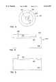
- FIG. 1is a perspective view of an embodiment of a system module according to the teachings of the present invention.
- FIG. 2is a cross sectional view of a semiconductor chip or die of the system module of FIG. 1.
- FIG. 3is a cross sectional view of an embodiment of a coaxial conductor.
- FIGS. 4, 5, 6, 7, 8, and 9are elevational views of a semiconductor wafer at various points of in illustrative embodiment of a method according to the teachings of the present invention.
- FIG. 10is a block diagram of an embodiment of an electronic system according to the teachings of the present invention.
- chip, die, wafer and substrateare interchangeably used to refer generally to any structure, or portion of a structure, on which integrated circuits are formed, and also to such structures during various stages of integrated circuit fabrication.
- the termsinclude doped and undoped semiconductors, epitaxial layers of a semiconductor on a supporting semiconductor or insulating material, combinations of such layers, as well as other such structures that are known in the art.
- horizontalas used in this application is defined as a plane parallel to the conventional plane or Surface of a wafer or substrate, regardless of the orientation of the wafer or substrate.
- verticalrefers to a direction perpendicular to the horizontal as defined above.
- Prepositions, such as “on”, “side” (as in “sidewall”), “higher”, “lower”, “over” and “under”are defined with respect to the conventional plane or surface being on the top surface of the wafer or substrate, regardless of the orientation of the wafer or substrate.
- FIG. 1is a perspective view of an embodiment of a system module, indicated generally at 100, according to the teachings of the present invention.
- System module 100includes a plurality of semiconductor chips 102-1, . . . , 102-N that are disposed and interconnected in a stack to provide "chip-sized" packaging.
- Each semiconductor chip 102-1, . . . , 102-Nincludes integrated circuits 106-1, . . . , 106-N, respectively.
- semiconductor chips 102-1, . . . , 102-Ncomprise semiconductor dies with memory circuits such as dynamic random access memory circuits.
- system module 100is a "memory module” or "memory cube.”
- integrated circuits 106-1, . . . ,106-Ncomprise other appropriate circuits such as logic circuits.
- System module 1,00uses microbumps 104 to interconnect the integrated circuits 106-1, . . . , 106-N.
- microbumps 104comprise controlled-collapse chip connections (C-4) solder pads. Other appropriate materials can be used to form microbumps 104.
- Microbumps 104are formed on first sides 108-1, . . . , 108-N and second sides 110-1, . . . , 110-N of semiconductor chips 102-1, . . . , 102-N.
- the microbumps 104are connected to coaxial conductors, described in more detail below, to carry signals between semiconductor wafers 102-1, . . . , 102-N.
- Microbumps 104are selectively formed using, for example, a vacuum deposition through a mask. The deposited material is then reflowed to homogenize lead and tin as the microbumps. Selected microbumps 104 are aligned and bonded, e.g., the microbumps indicated by arrow 112, by bringing the respective microbumps 104 into contact at an appropriate temperature.
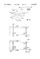
- FIG. 2is a cross sectional view of a semiconductor chip, indicated generally at 102-I, according to an embodiment of the present invention.
- Semiconductor chip 102-Iincludes coaxial conductors 202 that are formed in high aspect ratio vias through the thickness of semiconductor chip 102-I.
- the coaxial conductors 202have an aspect ratio in the range of approximately 100 to 200.
- a semiconductor wafer used to form an integrated circuithas a thickness in the range of approximately 500 to 1000 microns.
- the high aspect ratio viascan be fabricated with a width that is in the range from approximately 2.5 microns up to as much as approximately 10 microns.
- Coaxial conductcors 202include center conductor 204 that is surrounded by insulator, e.g., oxide, 206 ). Further, outer conductor 208 surrounds insulator 206. Coaxial conductor 202 is shown in cross section in FIG. 3. Outer conductor 208 comprises, for example, a metal layer that is deposited within the high aspect ratio via. Alternatively, outer conductor 208 may comprise a portion of semiconductor chip 102-1 that has been doped with impurities to render it conductive.
- Coaxial conductor 202is selectively coupled to integrated circuit 106-I using a metallization layer 210. Further, microbumps 104 are formed outwardly from the metallization layer 210 to provide for interconnection with other semiconductor wafers in a stack to form a system module.
- coaxial conductors 202allow a number of semiconductor wafers to be interconnected in a stack with an increased density over other system modules.
- the space between semiconductor wafers in system module 100is on the order of a few microns, e.g., the thickness of two bonded, solder microbumps. Assuming a wafer thickness on the order of 750 microns, eight semiconductor wafers can be stacked to form a system module with a thickness on the order of 6 millimeters. This compact system module can be readily mounted into a variety of system packages.
- microbumpsto interconnect the semiconductor wafers in a stack provides additional advantages. For example, stray capacitance, stray inductance and series resistance are all reduced over other system modules. This ultimately results in improved performance.
- the coaxial conductor 202 shown in FIGS. 2 and 3have, for simplicity, a geometry such that: ##EQU1##
- the capacitance of coaxial conductoris: ##EQU2##
- the term e r e ois the electric permittivity of insulator layer 206 and d is the length of coaxial conductor 202. If insulator layer 206 is silicon dioxide and the coaxial conductor has a length of approximately 750 microns, then the capacitance is approximately 50 femptofarads (fF).
- the inductancecan be calculated as follows: ##EQU3## In this equation, ⁇ 0 is the magnetic permeability of free space.
- thisprovides an inductance on the order of 0.5 nanohenries (nH). These values are less than those associated with a conventional wire bond, e.g., 500 to 1000 fF and 1-2 nH. Further, the large stray capacitances and inductances (1-7 picofarads (pF) and 2-35 nH) associated with a package and even larger capacitances and inductances associated with a printed circuit board are avoided.
- the microbumps of system 100have only a small stray capacitance, e.g., 100 to 500 fF, and a small inductance of less than 0.1 nH.
- the net resultis that the interconnection between the semiconductor chips 102-1, . . . , 102-N of system 100 can be made with about the same stray capacitance and inductance as that of a single wire bond.
- Alternative connection techniqueswould require significantly more wire bonds and huge stray inductances and capacitances associated with the packaging and even larger strays associated with interconnection of the packages.
- Coaxial conductors 202can be added to circuits using a conventional layout for the circuit without adversely affecting the surface area requirements of the circuit.
- Conventional circuitstypically include pads formed on the top surface of the semiconductor wafer that are used to connect to various signals for the system.
- the bond wires of conventional circuitscan be replaced by coaxial conductors 202 and microbumps 104 to achieve the advantages described above.
- FIGS. 4, 5, 6, 7, 8, and 9are elevational views of semiconductor chip 102-I at various points of an illustrative embodiment of a method for forming an integrated circuit with coaxial conductors according to the teachings of the present invention.
- Functional circuit 402is formed in an active region of semiconductor wafer 400.
- semiconductor wafer 400comprises a monocrystalline silicon wafer.
- the Figuresonly show the formation of two coaxial conductors through semiconductor wafer 400.
- any appropriate number of viascan be formed through semiconductor wafer 400.
- the number of vias needed for a conventional dynamic random access memory (DRAM)may be on the order of 100.
- DRAMdynamic random access memory
- the coaxial conductorsare formed in the same space on the surface of semiconductor wafer 400 that is conventionally used to form bond pads to be connected to leads.
- the coaxial conductorsreplace the conventional bond wires which couple the bond pads to selected leads of a lead frame in the packaging of the semiconductor wafer.
- photoresist layer 404is formed on surface 406 of semiconductor substrate 100. Photoresist layer 404 is patterned to provide openings 408 at points on surface 406 where high aspect ratio holes are to be formed through semiconductor wafer 400.
- etch pits 410are formed by conventional alkaline etching through openings 408 in photoresist layer 404. Photoresist layer 404 is then removed.
- FIG. 6is a schematic diagram that illustrates an embodiment of a layout of equipment used to carry out an anodic etch that is used to form high aspect ratio holes 450 of FIG. 7. 'Typically, holes 450 have an aspect ratio in the range of 100 to 200.
- Bottom surface 462 of semiconductor wafer 400is coupled to voltage source 434 by positive electrode 430.
- negative electrode 432is coupled to voltage source 434 and is placed in a bath of 6% aqueous solution of hydrofluoric acid (HF) on surface 406 of semiconductor wafer 400.
- HFhydrofluoric acid
- illumination equipment 436is also included because semiconductor wafer 400 is n-type semiconductor material. When p-type semiconductor material is used, the illumination equipment is not required. Illumination equipment 436 assures that there is a sufficient concentration of holes in semiconductor wafer 400 as required by the anodic etching process. Illumination equipment 436 includes lamp 438, IR filter 440, and lens 442. Illumination equipment 436 focuses light on surface 462 of semiconductor wafer 400.
- the anodic etchetches high aspect ratio holes through semiconductor wafer 400 at the location of etch pits 410.
- Voltage source 434is turned on and provides a voltage across positive and negative electrodes 430 and 432.
- Etching currentflows from positive electrode 430 to surface 406. This current forms the high aspect ratio holes through semiconductor wafer 400.
- illumination equipmentilluminates surface 462 of semiconductor wafer 400 so as to assure a sufficient concentration of holes for the anodic etching process.
- the size and shape of the high aspect ratio holes through semiconductor wafer 400depends on, for example, the anodization parameters such as HF concentration, current density, and light illumination.
- An anodic etching processis described in V. Lehmann, The Physics of Macropore Formation in Low Doped n-Type Silicon, J. Electrochem. Soc., Vol. 140, No. 10, pp. 2836-2843, Oct. 1993, which is incorporated herein by reference.
- FIG. 7illustrates the formation of the outer conductor 454 of a coaxial conductor.
- Outer conductor 454can be formed in at least one of two ways.
- outer conductor 454can be formed using a low pressure chemical vapor deposition of tungsten in a self-limiting process which provides a tungsten film on inner surface 452 of holes 450 by silicon reduction. Accordingly, silicon material within holes 450 is replaced by tungsten atoms in a WF 6 reaction gas.
- a reaction product, SiF 4is pumped out or otherwise removed from the reaction chamber. This can be followed by a silane or polysilane reduction of the WF 6 until a desired thickness is achieved. Deposition rates for this process are dependent on temperature and reaction gas flow rate. Deposition rates of 1 micron per minute have been observed at temperatures of 300° C. and with a flow rate of WF 6 at 4 sccm in a cold wall CVD reactor.
- outer conductor 454can be formed as diffusion regions within semiconductor wafer 400 along inner surface 450. To accomplish this, surfaces 406 and 462 are masked by a masking layer and conductivity enhancing impurities are introduced. The impurities form outer conductor 454 as, for example, n+ regions.
- FIG. 8 and 9illustrate the completion of the coaxial conductors.
- an insulator materiale.g., silicon dioxide
- Insulator layer 455is formed so as to leave an opening extending through the thickness of semiconductor wafer 400.
- hole 450is filled with a layer of polysilicon 456 by a process of chemical vapor deposition (CVD).
- CVDchemical vapor deposition
- polysiliconhas been deposited in holes with such high aspect ratios, e.g., deep trenches for trench capacitors.
- excess polysilicon on surface 406is removed by, for example, chemical/mechanical polishing.
- Aluminum layers 458 and 460are deposited on surfaces 406 and 462 using, for example, a sputtering technique used to coat optical disks. Layers 458 and 460 have a thickness on the order of a few microns.
- the structure shown in FIG. 8is then annealed at 500 degrees Celsius in Nitrogen ambient. This allows the aluminum material of layers 458 and 460 to be substituted for the polysilicon 456 in holes 450.
- the displaced polysilicon and any residual aluminum from layers 458 and 460are removed by, for example, chemical/mechanical polishing.
- a thin, e.g, 0.1 ⁇ m, layer of titanium on top of layers 458 and 460the above mentioned anneal can be reduced from 500° Celsius to 450° Celsius.
- the structureis now as shown in FIG. 9 with coaxial conductors 464 extending through semiconductor wafer 400.
- FIG. 10is a block diagram of an embodiment of an electronic system, indicated generally at 500, and constructed according to the teachings of the present invention.
- System 500includes processor 504 and memory module 502.
- Memory module 502includes a number of memory circuits that are fabricated on separate semiconductor chips or dies. These dies include a plurality of coaxial conductors that are formed through the thickness of their respective dies as described in more detail above. These coaxial conductors are interconnected with other semiconductor chips using a microbump bonding, e.g., C-4 type microbumps.
- the high aspect ratio viascan be applied in a wide variety of circuits including but not limited to dynamic random access memory devices, logic circuits, and other appropriate circuits. Further, other techniques can be used to form and fill the high aspect ratio holes to form the coaxial conductors. Further, the high aspect ratio vias can be filed with a conductive material without forming a coaxial conductor.
Landscapes
- Engineering & Computer Science (AREA)
- Power Engineering (AREA)
- Microelectronics & Electronic Packaging (AREA)
- Physics & Mathematics (AREA)
- Condensed Matter Physics & Semiconductors (AREA)
- General Physics & Mathematics (AREA)
- Computer Hardware Design (AREA)
- Internal Circuitry In Semiconductor Integrated Circuit Devices (AREA)
Abstract
Description
Claims (23)
Priority Applications (3)
| Application Number | Priority Date | Filing Date | Title |
|---|---|---|---|
| US09/198,554US6122187A (en) | 1998-11-23 | 1998-11-23 | Stacked integrated circuits |
| US09/665,255US6314013B1 (en) | 1998-11-23 | 2000-09-19 | Stacked integrated circuits |
| US09/854,809US6395630B2 (en) | 1998-11-23 | 2001-05-14 | Stacked integrated circuits |
Applications Claiming Priority (1)
| Application Number | Priority Date | Filing Date | Title |
|---|---|---|---|
| US09/198,554US6122187A (en) | 1998-11-23 | 1998-11-23 | Stacked integrated circuits |
Related Child Applications (1)
| Application Number | Title | Priority Date | Filing Date |
|---|---|---|---|
| US09/665,255ContinuationUS6314013B1 (en) | 1998-11-23 | 2000-09-19 | Stacked integrated circuits |
Publications (1)
| Publication Number | Publication Date |
|---|---|
| US6122187Atrue US6122187A (en) | 2000-09-19 |
Family
ID=22733871
Family Applications (3)
| Application Number | Title | Priority Date | Filing Date |
|---|---|---|---|
| US09/198,554Expired - LifetimeUS6122187A (en) | 1998-11-23 | 1998-11-23 | Stacked integrated circuits |
| US09/665,255Expired - Fee RelatedUS6314013B1 (en) | 1998-11-23 | 2000-09-19 | Stacked integrated circuits |
| US09/854,809Expired - LifetimeUS6395630B2 (en) | 1998-11-23 | 2001-05-14 | Stacked integrated circuits |
Family Applications After (2)
| Application Number | Title | Priority Date | Filing Date |
|---|---|---|---|
| US09/665,255Expired - Fee RelatedUS6314013B1 (en) | 1998-11-23 | 2000-09-19 | Stacked integrated circuits |
| US09/854,809Expired - LifetimeUS6395630B2 (en) | 1998-11-23 | 2001-05-14 | Stacked integrated circuits |
Country Status (1)
| Country | Link |
|---|---|
| US (3) | US6122187A (en) |
Cited By (20)
| Publication number | Priority date | Publication date | Assignee | Title |
|---|---|---|---|---|
| US20020109133A1 (en)* | 1999-02-23 | 2002-08-15 | Junichi Hikita | Semiconductor chip and semiconductor device using the same, and method of fabricating semiconductor chip |
| US20020115260A1 (en)* | 2001-02-22 | 2002-08-22 | Halahan Patrick B. | Semiconductor structures having multiple conductive layers in an opening, and methods for fabricating same |
| US20030001236A1 (en)* | 2001-05-31 | 2003-01-02 | Harry Hedler | Semiconductor chip, memory module and method for testing the semiconductor chip |
| WO2002063686A3 (en)* | 2001-02-08 | 2003-02-20 | Micron Technology Inc | High performance silicon contact for flip chip |
| US6526191B1 (en) | 1998-02-26 | 2003-02-25 | Micron Technology, Inc. | Integrated circuits using optical fiber interconnects formed through a semiconductor wafer and methods for forming same |
| US6534874B1 (en)* | 1999-11-02 | 2003-03-18 | Matsushita Electronics Corporation | Semiconductor device and method of producing the same |
| US6542393B1 (en) | 2002-04-24 | 2003-04-01 | Ma Laboratories, Inc. | Dual-bank memory module with stacked DRAM chips having a concave-shaped re-route PCB in-between |
| US6594171B1 (en)* | 2002-03-07 | 2003-07-15 | Hewlett-Packard Development Company, L.P. | Memory systems and methods of making the same |
| US20030197186A1 (en)* | 1998-02-26 | 2003-10-23 | Micron Technology, Inc. | Integrated circuits using optical waveguide interconnects formed through a semiconductor wafer and methods for forming same |
| US6709978B2 (en)* | 1998-01-20 | 2004-03-23 | Micron Technology, Inc. | Method for forming integrated circuits using high aspect ratio vias through a semiconductor wafer |
| US6734538B1 (en) | 2001-04-12 | 2004-05-11 | Bae Systems Information & Electronic Systems Integration, Inc. | Article comprising a multi-layer electronic package and method therefor |
| US20050046034A1 (en)* | 2003-09-03 | 2005-03-03 | Micron Technology, Inc. | Apparatus and method for high density multi-chip structures |
| US20080116584A1 (en)* | 2006-11-21 | 2008-05-22 | Arkalgud Sitaram | Self-aligned through vias for chip stacking |
| US20080277799A1 (en)* | 2004-08-27 | 2008-11-13 | Micron Technology, Inc. | Low temperature methods of forming back side redistribution layers in association with through wafer interconnects, semiconductor devices including same, and assemblies |
| US20080296763A1 (en)* | 2007-05-31 | 2008-12-04 | Chen-Shien Chen | Multi-Die Wafer Level Packaging |
| US20110139497A1 (en)* | 2009-12-14 | 2011-06-16 | Qualcomm Incorporated | Via Structure Integrated in Electronic Substrate |
| US20120091567A1 (en)* | 2009-03-13 | 2012-04-19 | Stats Chippac, Ltd. | Semiconductor Die and Method of Forming Noise Absorbing Regions Between THVs in Peripheral Region of the Die |
| WO2012171742A1 (en)* | 2011-06-16 | 2012-12-20 | Ams Ag | Method for producing a semiconductor component comprising a conductor layer in the semiconductor body and semiconductor component |
| CN104051426A (en)* | 2013-03-13 | 2014-09-17 | 阿尔特拉公司 | Apparatus for electronic assembly with improved interconnect and associated methods |
| US10686534B2 (en) | 2018-04-05 | 2020-06-16 | Korea Institute Of Science And Technology | Method for optical interconnection between semiconductor chips using mid-infrared |
Families Citing this family (61)
| Publication number | Priority date | Publication date | Assignee | Title |
|---|---|---|---|---|
| US7157314B2 (en) | 1998-11-16 | 2007-01-02 | Sandisk Corporation | Vertically stacked field programmable nonvolatile memory and method of fabrication |
| US6683372B1 (en) | 1999-11-18 | 2004-01-27 | Sun Microsystems, Inc. | Memory expansion module with stacked memory packages and a serial storage unit |
| US8575719B2 (en) | 2000-04-28 | 2013-11-05 | Sandisk 3D Llc | Silicon nitride antifuse for use in diode-antifuse memory arrays |
| US6888750B2 (en) | 2000-04-28 | 2005-05-03 | Matrix Semiconductor, Inc. | Nonvolatile memory on SOI and compound semiconductor substrates and method of fabrication |
| KR100821456B1 (en) | 2000-08-14 | 2008-04-11 | 샌디스크 쓰리디 엘엘씨 | Dense array and charge storage device and manufacturing method thereof |
| US7352199B2 (en)* | 2001-02-20 | 2008-04-01 | Sandisk Corporation | Memory card with enhanced testability and methods of making and using the same |
| US6897514B2 (en) | 2001-03-28 | 2005-05-24 | Matrix Semiconductor, Inc. | Two mask floating gate EEPROM and method of making |
| JP2002305282A (en)* | 2001-04-06 | 2002-10-18 | Shinko Electric Ind Co Ltd | Semiconductor element and structure for connecting the same, and semiconductor device with stacked semiconductor elements |
| US6843421B2 (en) | 2001-08-13 | 2005-01-18 | Matrix Semiconductor, Inc. | Molded memory module and method of making the module absent a substrate support |
| US6841813B2 (en) | 2001-08-13 | 2005-01-11 | Matrix Semiconductor, Inc. | TFT mask ROM and method for making same |
| US6593624B2 (en) | 2001-09-25 | 2003-07-15 | Matrix Semiconductor, Inc. | Thin film transistors with vertically offset drain regions |
| US6525953B1 (en) | 2001-08-13 | 2003-02-25 | Matrix Semiconductor, Inc. | Vertically-stacked, field-programmable, nonvolatile memory and method of fabrication |
| US6750516B2 (en)* | 2001-10-18 | 2004-06-15 | Hewlett-Packard Development Company, L.P. | Systems and methods for electrically isolating portions of wafers |
| US6624485B2 (en) | 2001-11-05 | 2003-09-23 | Matrix Semiconductor, Inc. | Three-dimensional, mask-programmed read only memory |
| JP3495727B2 (en)* | 2001-11-07 | 2004-02-09 | 新光電気工業株式会社 | Semiconductor package and manufacturing method thereof |
| EP1472730A4 (en)* | 2002-01-16 | 2010-04-14 | Mann Alfred E Found Scient Res | HOUSING FOR ELECTRONIC CIRCUITS WITH REDUCED SIZE |
| US6731011B2 (en) | 2002-02-19 | 2004-05-04 | Matrix Semiconductor, Inc. | Memory module having interconnected and stacked integrated circuits |
| US6853049B2 (en) | 2002-03-13 | 2005-02-08 | Matrix Semiconductor, Inc. | Silicide-silicon oxide-semiconductor antifuse device and method of making |
| US6737675B2 (en) | 2002-06-27 | 2004-05-18 | Matrix Semiconductor, Inc. | High density 3D rail stack arrays |
| US6841883B1 (en) | 2003-03-31 | 2005-01-11 | Micron Technology, Inc. | Multi-dice chip scale semiconductor components and wafer level methods of fabrication |
| US8471263B2 (en)* | 2003-06-24 | 2013-06-25 | Sang-Yun Lee | Information storage system which includes a bonded semiconductor structure |
| US6864171B1 (en)* | 2003-10-09 | 2005-03-08 | Infineon Technologies Ag | Via density rules |
| US7030470B1 (en) | 2004-05-11 | 2006-04-18 | Sun Microsystems, Inc. | Using chip lamination to couple an integrated circuit with a microstrip transmission line |
| US7400047B2 (en)* | 2004-12-13 | 2008-07-15 | Agere Systems Inc. | Integrated circuit with stacked-die configuration utilizing substrate conduction |
| US7317256B2 (en)* | 2005-06-01 | 2008-01-08 | Intel Corporation | Electronic packaging including die with through silicon via |
| US7560813B2 (en) | 2005-06-14 | 2009-07-14 | John Trezza | Chip-based thermo-stack |
| US7781886B2 (en) | 2005-06-14 | 2010-08-24 | John Trezza | Electronic chip contact structure |
| US7851348B2 (en) | 2005-06-14 | 2010-12-14 | Abhay Misra | Routingless chip architecture |
| US7838997B2 (en) | 2005-06-14 | 2010-11-23 | John Trezza | Remote chip attachment |
| US7534722B2 (en) | 2005-06-14 | 2009-05-19 | John Trezza | Back-to-front via process |
| US7767493B2 (en) | 2005-06-14 | 2010-08-03 | John Trezza | Post & penetration interconnection |
| US7687400B2 (en) | 2005-06-14 | 2010-03-30 | John Trezza | Side stacking apparatus and method |
| WO2006138492A2 (en)* | 2005-06-14 | 2006-12-28 | Cubic Wafer, Inc. | Post & penetration interconnection |
| US7989958B2 (en) | 2005-06-14 | 2011-08-02 | Cufer Assett Ltd. L.L.C. | Patterned contact |
| US7786592B2 (en) | 2005-06-14 | 2010-08-31 | John Trezza | Chip capacitive coupling |
| US7521806B2 (en) | 2005-06-14 | 2009-04-21 | John Trezza | Chip spanning connection |
| US8456015B2 (en) | 2005-06-14 | 2013-06-04 | Cufer Asset Ltd. L.L.C. | Triaxial through-chip connection |
| US7465652B2 (en) | 2005-08-16 | 2008-12-16 | Sony Corporation | Method of forming a catalyst layer on the barrier layer of a conductive interconnect of a semiconductor device |
| US7422975B2 (en) | 2005-08-18 | 2008-09-09 | Sony Corporation | Composite inter-level dielectric structure for an integrated circuit |
| US8586468B2 (en) | 2005-08-24 | 2013-11-19 | Sony Corporation | Integrated circuit chip stack employing carbon nanotube interconnects |
| EP1922756B1 (en)* | 2005-08-26 | 2013-05-22 | Philips Intellectual Property & Standards GmbH | Electrically shielded through-wafer interconnect |
| US7251799B2 (en) | 2005-08-30 | 2007-07-31 | Sony Corporation | Metal interconnect structure for integrated circuits and a design rule therefor |
| KR100713121B1 (en)* | 2005-09-27 | 2007-05-02 | 한국전자통신연구원 | Chips and Chip Stacks Using the Same |
| US7798817B2 (en)* | 2005-11-04 | 2010-09-21 | Georgia Tech Research Corporation | Integrated circuit interconnects with coaxial conductors |
| US7687397B2 (en) | 2006-06-06 | 2010-03-30 | John Trezza | Front-end processed wafer having through-chip connections |
| JP5269799B2 (en)* | 2006-10-17 | 2013-08-21 | キューファー アセット リミテッド. エル.エル.シー. | Wafer via formation |
| US7705613B2 (en)* | 2007-01-03 | 2010-04-27 | Abhay Misra | Sensitivity capacitive sensor |
| US7803693B2 (en)* | 2007-02-15 | 2010-09-28 | John Trezza | Bowed wafer hybridization compensation |
| US7598163B2 (en)* | 2007-02-15 | 2009-10-06 | John Callahan | Post-seed deposition process |
| US7705632B2 (en)* | 2007-02-15 | 2010-04-27 | Wyman Theodore J Ted | Variable off-chip drive |
| US7670874B2 (en)* | 2007-02-16 | 2010-03-02 | John Trezza | Plated pillar package formation |
| US7747223B2 (en)* | 2007-03-29 | 2010-06-29 | Research In Motion Limited | Method, system and mobile device for prioritizing a discovered device list |
| US7748116B2 (en)* | 2007-04-05 | 2010-07-06 | John Trezza | Mobile binding in an electronic connection |
| US7850060B2 (en)* | 2007-04-05 | 2010-12-14 | John Trezza | Heat cycle-able connection |
| US20080261392A1 (en)* | 2007-04-23 | 2008-10-23 | John Trezza | Conductive via formation |
| US7960210B2 (en)* | 2007-04-23 | 2011-06-14 | Cufer Asset Ltd. L.L.C. | Ultra-thin chip packaging |
| US20100065949A1 (en)* | 2008-09-17 | 2010-03-18 | Andreas Thies | Stacked Semiconductor Chips with Through Substrate Vias |
| JP2010080752A (en)* | 2008-09-26 | 2010-04-08 | Panasonic Corp | Method of manufacturing semiconductor device |
| US9627395B2 (en) | 2015-02-11 | 2017-04-18 | Sandisk Technologies Llc | Enhanced channel mobility three-dimensional memory structure and method of making thereof |
| US9478495B1 (en) | 2015-10-26 | 2016-10-25 | Sandisk Technologies Llc | Three dimensional memory device containing aluminum source contact via structure and method of making thereof |
| US11481299B2 (en) | 2019-12-04 | 2022-10-25 | Micron Technology, Inc. | Transmission of data for a machine learning operation using different microbumps |
Citations (28)
| Publication number | Priority date | Publication date | Assignee | Title |
|---|---|---|---|---|
| US4394712A (en)* | 1981-03-18 | 1983-07-19 | General Electric Company | Alignment-enhancing feed-through conductors for stackable silicon-on-sapphire wafers |
| US5200917A (en)* | 1991-11-27 | 1993-04-06 | Micron Technology, Inc. | Stacked printed circuit board device |
| WO1994005039A1 (en)* | 1992-08-20 | 1994-03-03 | Capps David A | Semiconductor wafer for lamination applications |
| US5352998A (en)* | 1992-10-09 | 1994-10-04 | Mitsubishi Denki Kabushiki Kaisha | Microwave integrated circuit having a passive circuit substrate mounted on a semiconductor circuit substrate |
| US5362976A (en)* | 1991-10-26 | 1994-11-08 | Nec Corporation | High frequency semiconductor device having optical guide package structure |
| US5399898A (en)* | 1992-07-17 | 1995-03-21 | Lsi Logic Corporation | Multi-chip semiconductor arrangements using flip chip dies |
| US5404044A (en)* | 1992-09-29 | 1995-04-04 | International Business Machines Corporation | Parallel process interposer (PPI) |
| US5432729A (en)* | 1993-04-23 | 1995-07-11 | Irvine Sensors Corporation | Electronic module comprising a stack of IC chips each interacting with an IC chip secured to the stack |
| US5434452A (en)* | 1993-11-01 | 1995-07-18 | Motorola, Inc. | Z-axis compliant mechanical IC wiring substrate and method for making the same |
| US5532506A (en)* | 1994-08-31 | 1996-07-02 | Texas Instruments Incorporated | Integrated circuit adapted for improved thermal impedance |
| US5578526A (en)* | 1992-03-06 | 1996-11-26 | Micron Technology, Inc. | Method for forming a multi chip module (MCM) |
| US5608265A (en)* | 1993-03-17 | 1997-03-04 | Hitachi, Ltd. | Encapsulated semiconductor device package having holes for electrically conductive material |
| US5656548A (en)* | 1993-09-30 | 1997-08-12 | Kopin Corporation | Method for forming three dimensional processor using transferred thin film circuits |
| US5661901A (en)* | 1995-07-10 | 1997-09-02 | Micron Technology, Inc. | Method for mounting and electrically interconnecting semiconductor dice |
| US5682062A (en)* | 1995-06-05 | 1997-10-28 | Harris Corporation | System for interconnecting stacked integrated circuits |
| US5696031A (en)* | 1996-11-20 | 1997-12-09 | Micron Technology, Inc. | Device and method for stacking wire-bonded integrated circuit dice on flip-chip bonded integrated circuit dice |
| US5767001A (en)* | 1993-05-05 | 1998-06-16 | Siemens Aktiengesellschaft | Process for producing semiconductor components between which contact is made vertically |
| US5783870A (en)* | 1995-03-16 | 1998-07-21 | National Semiconductor Corporation | Method for connecting packages of a stacked ball grid array structure |
| US5789271A (en)* | 1996-03-18 | 1998-08-04 | Micron Technology, Inc. | Method for fabricating microbump interconnect for bare semiconductor dice |
| US5801452A (en)* | 1996-10-25 | 1998-09-01 | Micron Technology, Inc. | Multi chip module including semiconductor wafer or dice, interconnect substrate, and alignment member |
| US5808360A (en)* | 1996-05-15 | 1998-09-15 | Micron Technology, Inc. | Microbump interconnect for bore semiconductor dice |
| US5818697A (en)* | 1997-03-21 | 1998-10-06 | International Business Machines Corporation | Flexible thin film ball grid array containing solder mask |
| US5901050A (en)* | 1996-08-21 | 1999-05-04 | Ngk Spark Plug Co., Ltd. | Wired base plate and package for electronic parts |
| US5902118A (en)* | 1994-07-05 | 1999-05-11 | Siemens Aktiengesellschaft | Method for production of a three-dimensional circuit arrangement |
| US5903045A (en)* | 1996-04-30 | 1999-05-11 | International Business Machines Corporation | Self-aligned connector for stacked chip module |
| US5915167A (en)* | 1997-04-04 | 1999-06-22 | Elm Technology Corporation | Three dimensional structure memory |
| US5973392A (en)* | 1997-04-02 | 1999-10-26 | Nec Corporation | Stacked carrier three-dimensional memory module and semiconductor device using the same |
| US5995379A (en)* | 1997-10-30 | 1999-11-30 | Nec Corporation | Stacked module and substrate therefore |
Family Cites Families (5)
| Publication number | Priority date | Publication date | Assignee | Title |
|---|---|---|---|---|
| US3698082A (en)* | 1966-04-25 | 1972-10-17 | Texas Instruments Inc | Complex circuit array method |
| US5128831A (en)* | 1991-10-31 | 1992-07-07 | Micron Technology, Inc. | High-density electronic package comprising stacked sub-modules which are electrically interconnected by solder-filled vias |
| US5587119A (en)* | 1994-09-14 | 1996-12-24 | E-Systems, Inc. | Method for manufacturing a coaxial interconnect |
| US5814889A (en)* | 1995-06-05 | 1998-09-29 | Harris Corporation | Intergrated circuit with coaxial isolation and method |
| US6143616A (en)* | 1997-08-22 | 2000-11-07 | Micron Technology, Inc. | Methods of forming coaxial integrated circuitry interconnect lines |
- 1998
- 1998-11-23USUS09/198,554patent/US6122187A/ennot_activeExpired - Lifetime
- 2000
- 2000-09-19USUS09/665,255patent/US6314013B1/ennot_activeExpired - Fee Related
- 2001
- 2001-05-14USUS09/854,809patent/US6395630B2/ennot_activeExpired - Lifetime
Patent Citations (29)
| Publication number | Priority date | Publication date | Assignee | Title |
|---|---|---|---|---|
| US4394712A (en)* | 1981-03-18 | 1983-07-19 | General Electric Company | Alignment-enhancing feed-through conductors for stackable silicon-on-sapphire wafers |
| US5362976A (en)* | 1991-10-26 | 1994-11-08 | Nec Corporation | High frequency semiconductor device having optical guide package structure |
| US5200917A (en)* | 1991-11-27 | 1993-04-06 | Micron Technology, Inc. | Stacked printed circuit board device |
| US5578526A (en)* | 1992-03-06 | 1996-11-26 | Micron Technology, Inc. | Method for forming a multi chip module (MCM) |
| US5399898A (en)* | 1992-07-17 | 1995-03-21 | Lsi Logic Corporation | Multi-chip semiconductor arrangements using flip chip dies |
| WO1994005039A1 (en)* | 1992-08-20 | 1994-03-03 | Capps David A | Semiconductor wafer for lamination applications |
| US5404044A (en)* | 1992-09-29 | 1995-04-04 | International Business Machines Corporation | Parallel process interposer (PPI) |
| US5352998A (en)* | 1992-10-09 | 1994-10-04 | Mitsubishi Denki Kabushiki Kaisha | Microwave integrated circuit having a passive circuit substrate mounted on a semiconductor circuit substrate |
| US5608265A (en)* | 1993-03-17 | 1997-03-04 | Hitachi, Ltd. | Encapsulated semiconductor device package having holes for electrically conductive material |
| US5432729A (en)* | 1993-04-23 | 1995-07-11 | Irvine Sensors Corporation | Electronic module comprising a stack of IC chips each interacting with an IC chip secured to the stack |
| US5767001A (en)* | 1993-05-05 | 1998-06-16 | Siemens Aktiengesellschaft | Process for producing semiconductor components between which contact is made vertically |
| US5656548A (en)* | 1993-09-30 | 1997-08-12 | Kopin Corporation | Method for forming three dimensional processor using transferred thin film circuits |
| US5434452A (en)* | 1993-11-01 | 1995-07-18 | Motorola, Inc. | Z-axis compliant mechanical IC wiring substrate and method for making the same |
| US5902118A (en)* | 1994-07-05 | 1999-05-11 | Siemens Aktiengesellschaft | Method for production of a three-dimensional circuit arrangement |
| US5532506A (en)* | 1994-08-31 | 1996-07-02 | Texas Instruments Incorporated | Integrated circuit adapted for improved thermal impedance |
| US5783870A (en)* | 1995-03-16 | 1998-07-21 | National Semiconductor Corporation | Method for connecting packages of a stacked ball grid array structure |
| US5682062A (en)* | 1995-06-05 | 1997-10-28 | Harris Corporation | System for interconnecting stacked integrated circuits |
| US5661901A (en)* | 1995-07-10 | 1997-09-02 | Micron Technology, Inc. | Method for mounting and electrically interconnecting semiconductor dice |
| US5789271A (en)* | 1996-03-18 | 1998-08-04 | Micron Technology, Inc. | Method for fabricating microbump interconnect for bare semiconductor dice |
| US5903045A (en)* | 1996-04-30 | 1999-05-11 | International Business Machines Corporation | Self-aligned connector for stacked chip module |
| US5808360A (en)* | 1996-05-15 | 1998-09-15 | Micron Technology, Inc. | Microbump interconnect for bore semiconductor dice |
| US5834366A (en)* | 1996-05-15 | 1998-11-10 | Micron Technology, Inc. | Method for fabricating microbump interconnect for bare semiconductor dice |
| US5901050A (en)* | 1996-08-21 | 1999-05-04 | Ngk Spark Plug Co., Ltd. | Wired base plate and package for electronic parts |
| US5801452A (en)* | 1996-10-25 | 1998-09-01 | Micron Technology, Inc. | Multi chip module including semiconductor wafer or dice, interconnect substrate, and alignment member |
| US5696031A (en)* | 1996-11-20 | 1997-12-09 | Micron Technology, Inc. | Device and method for stacking wire-bonded integrated circuit dice on flip-chip bonded integrated circuit dice |
| US5818697A (en)* | 1997-03-21 | 1998-10-06 | International Business Machines Corporation | Flexible thin film ball grid array containing solder mask |
| US5973392A (en)* | 1997-04-02 | 1999-10-26 | Nec Corporation | Stacked carrier three-dimensional memory module and semiconductor device using the same |
| US5915167A (en)* | 1997-04-04 | 1999-06-22 | Elm Technology Corporation | Three dimensional structure memory |
| US5995379A (en)* | 1997-10-30 | 1999-11-30 | Nec Corporation | Stacked module and substrate therefore |
Non-Patent Citations (22)
| Title |
|---|
| Bauer, C.E., "Three Dimensional Multichip Modules", Proceedings of the Technical Program--National Electronic Packaging and Production Conference, NEPCON West '94, 2444, 2001-2005, (Mar. 1993). |
| Bauer, C.E., Three Dimensional Multichip Modules , Proceedings of the Technical Program National Electronic Packaging and Production Conference, NEPCON West 94, 2444, 2001 2005, (Mar. 1993).* |
| Ganasan, J.R., "3 D Packaging--Combining Chip on Chip (COC) and Chip on board (COB) Packages--Process and Design Considerations", Proceedings of 1997 Electronic Components and Technology Conference, 1210-1213, (1997) No Month. |
| Ganasan, J.R., 3 D Packaging Combining Chip on Chip (COC) and Chip on board (COB) Packages Process and Design Considerations , Proceedings of 1997 Electronic Components and Technology Conference, 1210 1213, (1997) No Month.* |
| Horie, H., et al., "Novel High Aspect Ratio Aluminum Plug for Logic /DRAM LSI's Using Polysilicon-Aluminum Substitute", Technical Digest: IEEE International Electron Devices Meeting, San Francisco, CA, 946-948, (1996) No Month. |
| Horie, H., et al., Novel High Aspect Ratio Aluminum Plug for Logic /DRAM LSI s Using Polysilicon Aluminum Substitute , Technical Digest: IEEE International Electron Devices Meeting, San Francisco, CA, 946 948, (1996) No Month.* |
| Lehmann, V., "The Physics of Macropore Formation in Low Doped n-Type Silicon", Journal of the Electrochemical Society, 140 (10), 2836-2843, (Oct. 1993). |
| Lehmann, V., The Physics of Macropore Formation in Low Doped n Type Silicon , Journal of the Electrochemical Society, 140 (10), 2836 2843, (Oct. 1993).* |
| Mimura, T., et al., "System Module: a New Chip-on-Chip Module Technology", Proceedings of IEEE Custom Integrated Circuit Conference, 439-442 (1997) No Month. |
| Mimura, T., et al., System Module: a New Chip on Chip Module Technology , Proceedings of IEEE Custom Integrated Circuit Conference, 439 442 (1997) No Month.* |
| Rabaey, J.M., "Digital Integrated Circuits, a design perspective", Prentice Hall , Upper Saddle River, NJ, 478, (1996) No Month. |
| Rabaey, J.M., Digital Integrated Circuits, a design perspective , Prentice Hall , Upper Saddle River, NJ, 478, (1996) No Month.* |
| Ramo, S., et al., "Fields and Waves in Communication Electronics", John Wiley & Sons, Inc., New York, 3rd ed., 250, (1994) No Month. |
| Ramo, S., et al., Fields and Waves in Communication Electronics , John Wiley & Sons, Inc. , New York, 3rd ed., 250, (1994) No Month.* |
| Senba, N., et al., "Application of 3-Dimensional Memory Module", Proceedings of 1996 International Symposium on Microelectronics, SPIE 2920, 279-84, (1996) No Month. |
| Senba, N., et al., Application of 3 Dimensional Memory Module , Proceedings of 1996 International Symposium on Microelectronics, SPIE 2920, 279 84, (1996) No Month.* |
| Seraphim, D.P., et al., "Principles of Electronic Packing."In: Principles of Electronic Packing, McGraw-Hill, New York, NY, 44, 190, 595-597, (1989) no month. |
| Seraphim, D.P., et al., Principles of Electronic Packing. In: Principles of Electronic Packing , McGraw Hill, New York, NY, 44, 190, 595 597, (1989) no month.* |
| Shibuya, A., et al., "New MCM Composed of D/L Base Substrate, High-Density-Wiring CSP and 3D Memory Modules", Proceedings of 1997 Electronic Components and Technology Conference, 491-496, (1997) no month. |
| Shibuya, A., et al., New MCM Composed of D/L Base Substrate, High Density Wiring CSP and 3D Memory Modules , Proceedings of 1997 Electronic Components and Technology Conference , 491 496, (1997) no month.* |
| Val, et al., "The 3D Interconnection --Applications for Mass Memories and Microelectronics", ISHIM 1991 Proceedings of the International Symposium on Microelctronics, 62-68, (1991) no month. |
| Val, et al., The 3D Interconnection Applications for Mass Memories and Microelectronics , ISHIM 1991 Proceedings of the International Symposium on Microelctronics , 62 68, (1991) no month.* |
Cited By (54)
| Publication number | Priority date | Publication date | Assignee | Title |
|---|---|---|---|---|
| US6709978B2 (en)* | 1998-01-20 | 2004-03-23 | Micron Technology, Inc. | Method for forming integrated circuits using high aspect ratio vias through a semiconductor wafer |
| US6995441B2 (en)* | 1998-02-26 | 2006-02-07 | Micron Technology, Inc. | Integrated circuits using optical waveguide interconnects formed through a semiconductor wafer and methods for forming same |
| US6723577B1 (en) | 1998-02-26 | 2004-04-20 | Micron Technology, Inc. | Method of forming an optical fiber interconnect through a semiconductor wafer |
| US6777715B1 (en) | 1998-02-26 | 2004-08-17 | Micron Technology, Inc. | Integrated circuits using optical waveguide interconnects formed through a semiconductor wafer and methods for forming same |
| US20060131684A1 (en)* | 1998-02-26 | 2006-06-22 | Micron Technology, Inc. | Integrated circuits using optical waveguide interconnects formed through a semiconductor wafer and methods for forming same |
| US20040156578A1 (en)* | 1998-02-26 | 2004-08-12 | Micron Technology, Inc. | Integrated circuits using optical fiber interconnects formed through a semiconductor wafer |
| US20070114543A1 (en)* | 1998-02-26 | 2007-05-24 | Micron Technology, Inc. | Electronic systems using optical waveguide interconnects formed through a semiconductor wafer |
| US7164156B2 (en) | 1998-02-26 | 2007-01-16 | Micron Technology, Inc. | Electronic systems using optical waveguide interconnects formed throught a semiconductor wafer |
| US20030197186A1 (en)* | 1998-02-26 | 2003-10-23 | Micron Technology, Inc. | Integrated circuits using optical waveguide interconnects formed through a semiconductor wafer and methods for forming same |
| US7547954B2 (en) | 1998-02-26 | 2009-06-16 | Micron Technology, Inc. | Electronic systems using optical waveguide interconnects formed through a semiconductor wafer |
| US6995443B2 (en) | 1998-02-26 | 2006-02-07 | Micron Technology, Inc. | Integrated circuits using optical fiber interconnects formed through a semiconductor wafer |
| US6526191B1 (en) | 1998-02-26 | 2003-02-25 | Micron Technology, Inc. | Integrated circuits using optical fiber interconnects formed through a semiconductor wafer and methods for forming same |
| US7589415B2 (en)* | 1999-02-23 | 2009-09-15 | Rohm Co., Ltd. | Semiconductor chip and semiconductor device using the same, and method of fabricating semiconductor chip |
| US20020109133A1 (en)* | 1999-02-23 | 2002-08-15 | Junichi Hikita | Semiconductor chip and semiconductor device using the same, and method of fabricating semiconductor chip |
| US6534874B1 (en)* | 1999-11-02 | 2003-03-18 | Matsushita Electronics Corporation | Semiconductor device and method of producing the same |
| US6737740B2 (en) | 2001-02-08 | 2004-05-18 | Micron Technology, Inc. | High performance silicon contact for flip chip |
| US20030207566A1 (en)* | 2001-02-08 | 2003-11-06 | Leonard Forbes | High performance silicon contact for flip chip |
| WO2002063686A3 (en)* | 2001-02-08 | 2003-02-20 | Micron Technology Inc | High performance silicon contact for flip chip |
| US6812137B2 (en) | 2001-02-08 | 2004-11-02 | Micron Technology, Inc. | Method of forming coaxial integrated circuitry interconnect lines |
| US6828656B2 (en) | 2001-02-08 | 2004-12-07 | Micron Technology, Inc. | High performance silicon contact for flip chip and a system using same |
| US7001825B2 (en) | 2001-02-22 | 2006-02-21 | Tru-Si Technologies, Inc. | Semiconductor structures having multiple conductive layers in an opening, and methods for fabricating same |
| US20050106845A1 (en)* | 2001-02-22 | 2005-05-19 | Halahan Patrick B. | Semiconductor structures having multiple conductive layers in an opening, and methods for fabricating same |
| US6844241B2 (en) | 2001-02-22 | 2005-01-18 | Tru-Si Technologies, Inc. | Fabrication of semiconductor structures having multiple conductive layers in an opening |
| US20020115260A1 (en)* | 2001-02-22 | 2002-08-22 | Halahan Patrick B. | Semiconductor structures having multiple conductive layers in an opening, and methods for fabricating same |
| WO2002078087A3 (en)* | 2001-02-22 | 2003-11-20 | Tru Si Technologies Inc | Semiconductor chip having multiple conductive layers in an opening, and method for fabricating same |
| US6734538B1 (en) | 2001-04-12 | 2004-05-11 | Bae Systems Information & Electronic Systems Integration, Inc. | Article comprising a multi-layer electronic package and method therefor |
| US6744127B2 (en)* | 2001-05-31 | 2004-06-01 | Infineon Technologies Ag | Semiconductor chip, memory module and method for testing the semiconductor chip |
| US20030001236A1 (en)* | 2001-05-31 | 2003-01-02 | Harry Hedler | Semiconductor chip, memory module and method for testing the semiconductor chip |
| US6594171B1 (en)* | 2002-03-07 | 2003-07-15 | Hewlett-Packard Development Company, L.P. | Memory systems and methods of making the same |
| US6542393B1 (en) | 2002-04-24 | 2003-04-01 | Ma Laboratories, Inc. | Dual-bank memory module with stacked DRAM chips having a concave-shaped re-route PCB in-between |
| US7560305B2 (en) | 2003-09-03 | 2009-07-14 | Micron Technology, Inc. | Apparatus and method for high density multi-chip structures |
| US20050046034A1 (en)* | 2003-09-03 | 2005-03-03 | Micron Technology, Inc. | Apparatus and method for high density multi-chip structures |
| US20140077393A1 (en)* | 2003-09-03 | 2014-03-20 | Micron Technology, Inc. | Apparatus and method for high density multi-chip structures |
| US9209127B2 (en)* | 2003-09-03 | 2015-12-08 | Micron Technology | Apparatus and method for high density multi-chip structures |
| US8592964B2 (en)* | 2003-09-03 | 2013-11-26 | Micron Technology, Inc. | Apparatus and method for high density multi-chip structures |
| US20060289990A1 (en)* | 2003-09-03 | 2006-12-28 | Micron Technology, Inc. | Apparatus and method for high density multi-chip structures |
| US20060063302A1 (en)* | 2003-09-03 | 2006-03-23 | Micron Technology, Inc. | Apparatus and method for high density multi-chip structures |
| US7994547B2 (en)* | 2004-08-27 | 2011-08-09 | Micron Technology, Inc. | Semiconductor devices and assemblies including back side redistribution layers in association with through wafer interconnects |
| US20080277799A1 (en)* | 2004-08-27 | 2008-11-13 | Micron Technology, Inc. | Low temperature methods of forming back side redistribution layers in association with through wafer interconnects, semiconductor devices including same, and assemblies |
| US20080116584A1 (en)* | 2006-11-21 | 2008-05-22 | Arkalgud Sitaram | Self-aligned through vias for chip stacking |
| US20090155957A1 (en)* | 2007-05-31 | 2009-06-18 | Chen-Shien Chen | Multi-Die Wafer Level Packaging |
| CN100592511C (en)* | 2007-05-31 | 2010-02-24 | 台湾积体电路制造股份有限公司 | Semiconductor packaging body |
| US7785927B2 (en) | 2007-05-31 | 2010-08-31 | Taiwan Semiconductor Manufacturing Company, Ltd. | Multi-die wafer level packaging |
| US7514797B2 (en)* | 2007-05-31 | 2009-04-07 | Taiwan Semiconductor Manufacturing Company, Ltd. | Multi-die wafer level packaging |
| US20080296763A1 (en)* | 2007-05-31 | 2008-12-04 | Chen-Shien Chen | Multi-Die Wafer Level Packaging |
| US9236352B2 (en)* | 2009-03-13 | 2016-01-12 | Stats Chippac, Ltd. | Semiconductor die and method of forming noise absorbing regions between THVs in peripheral region of the die |
| US20120091567A1 (en)* | 2009-03-13 | 2012-04-19 | Stats Chippac, Ltd. | Semiconductor Die and Method of Forming Noise Absorbing Regions Between THVs in Peripheral Region of the Die |
| US20110139497A1 (en)* | 2009-12-14 | 2011-06-16 | Qualcomm Incorporated | Via Structure Integrated in Electronic Substrate |
| US8227708B2 (en) | 2009-12-14 | 2012-07-24 | Qualcomm Incorporated | Via structure integrated in electronic substrate |
| WO2011075491A1 (en)* | 2009-12-14 | 2011-06-23 | Qualcomm Incorporated | Via structure integrated in electronic substrate |
| WO2012171742A1 (en)* | 2011-06-16 | 2012-12-20 | Ams Ag | Method for producing a semiconductor component comprising a conductor layer in the semiconductor body and semiconductor component |
| US9443759B2 (en) | 2011-06-16 | 2016-09-13 | Ams Ag | Method for producing a semiconductor device comprising a conductor layer in the semiconductor body and semiconductor body |
| CN104051426A (en)* | 2013-03-13 | 2014-09-17 | 阿尔特拉公司 | Apparatus for electronic assembly with improved interconnect and associated methods |
| US10686534B2 (en) | 2018-04-05 | 2020-06-16 | Korea Institute Of Science And Technology | Method for optical interconnection between semiconductor chips using mid-infrared |
Also Published As
| Publication number | Publication date |
|---|---|
| US20010033509A1 (en) | 2001-10-25 |
| US6314013B1 (en) | 2001-11-06 |
| US6395630B2 (en) | 2002-05-28 |
Similar Documents
| Publication | Publication Date | Title |
|---|---|---|
| US6122187A (en) | Stacked integrated circuits | |
| US6376909B1 (en) | Mixed-mode stacked integrated circuit with power supply circuit part of the stack | |
| US8018069B2 (en) | Through-hole contacts in a semiconductor device | |
| KR100552551B1 (en) | High Performance Silicon Contacts for Flip Chip | |
| US6962866B2 (en) | System-on-a-chip with multi-layered metallized through-hole interconnection | |
| US6709978B2 (en) | Method for forming integrated circuits using high aspect ratio vias through a semiconductor wafer | |
| JP4222929B2 (en) | Chip carrier | |
| US9123789B2 (en) | Chip with through silicon via electrode and method of forming the same | |
| US5196377A (en) | Method of fabricating silicon-based carriers | |
| US20070290300A1 (en) | Semiconductor device and method for manufacturing same | |
| US20070087528A1 (en) | Method and structure for vertically-stacked device contact | |
| KR20060033866A (en) | Electronic devices, assemblies and methods of manufacturing electronic devices | |
| US11652101B2 (en) | Trench capacitor assembly for high capacitance density | |
| CN115241165A (en) | Semiconductor device with recessed pads for die stack interconnect | |
| US20230009279A1 (en) | Semiconductor device with capacitor and method for forming the same | |
| CN116666382A (en) | Semiconductor structure and preparation method | |
| US20210287984A1 (en) | On integrated circuit (ic) device capacitor between metal lines | |
| US20250031393A1 (en) | Deep trench capacitor including stress-relief voids and methods of forming the same | |
| US12295149B2 (en) | Capacitor structure and method for forming the same | |
| CN116018060B (en) | Semiconductor structure, preparation method thereof and packaging structure | |
| JP7712305B2 (en) | Contact pads for three-dimensional memory devices and methods for manufacturing the same | |
| KR100744464B1 (en) | Integrated inductor and a method for manufacturing the same | |
| CN115377088B (en) | Recessed semiconductor device and associated systems and methods | |
| TW202408045A (en) | Semiconductor device and manufacturing method thereof |
Legal Events
| Date | Code | Title | Description |
|---|---|---|---|
| AS | Assignment | Owner name:MICRON TECHNOLOGY, INC., IDAHO Free format text:ASSIGNMENT OF ASSIGNORS INTEREST;ASSIGNORS:AHN, KIE Y.;FORBES, LEONARD;REEL/FRAME:009613/0044;SIGNING DATES FROM 19981031 TO 19981102 | |
| STCF | Information on status: patent grant | Free format text:PATENTED CASE | |
| FEPP | Fee payment procedure | Free format text:PAYOR NUMBER ASSIGNED (ORIGINAL EVENT CODE: ASPN); ENTITY STATUS OF PATENT OWNER: LARGE ENTITY | |
| FPAY | Fee payment | Year of fee payment:4 | |
| FPAY | Fee payment | Year of fee payment:8 | |
| FPAY | Fee payment | Year of fee payment:12 | |
| AS | Assignment | Owner name:U.S. BANK NATIONAL ASSOCIATION, AS COLLATERAL AGENT, CALIFORNIA Free format text:SECURITY INTEREST;ASSIGNOR:MICRON TECHNOLOGY, INC.;REEL/FRAME:038669/0001 Effective date:20160426 Owner name:U.S. BANK NATIONAL ASSOCIATION, AS COLLATERAL AGEN Free format text:SECURITY INTEREST;ASSIGNOR:MICRON TECHNOLOGY, INC.;REEL/FRAME:038669/0001 Effective date:20160426 | |
| AS | Assignment | Owner name:MORGAN STANLEY SENIOR FUNDING, INC., AS COLLATERAL AGENT, MARYLAND Free format text:PATENT SECURITY AGREEMENT;ASSIGNOR:MICRON TECHNOLOGY, INC.;REEL/FRAME:038954/0001 Effective date:20160426 Owner name:MORGAN STANLEY SENIOR FUNDING, INC., AS COLLATERAL Free format text:PATENT SECURITY AGREEMENT;ASSIGNOR:MICRON TECHNOLOGY, INC.;REEL/FRAME:038954/0001 Effective date:20160426 | |
| AS | Assignment | Owner name:U.S. BANK NATIONAL ASSOCIATION, AS COLLATERAL AGENT, CALIFORNIA Free format text:CORRECTIVE ASSIGNMENT TO CORRECT THE REPLACE ERRONEOUSLY FILED PATENT #7358718 WITH THE CORRECT PATENT #7358178 PREVIOUSLY RECORDED ON REEL 038669 FRAME 0001. ASSIGNOR(S) HEREBY CONFIRMS THE SECURITY INTEREST;ASSIGNOR:MICRON TECHNOLOGY, INC.;REEL/FRAME:043079/0001 Effective date:20160426 Owner name:U.S. BANK NATIONAL ASSOCIATION, AS COLLATERAL AGEN Free format text:CORRECTIVE ASSIGNMENT TO CORRECT THE REPLACE ERRONEOUSLY FILED PATENT #7358718 WITH THE CORRECT PATENT #7358178 PREVIOUSLY RECORDED ON REEL 038669 FRAME 0001. ASSIGNOR(S) HEREBY CONFIRMS THE SECURITY INTEREST;ASSIGNOR:MICRON TECHNOLOGY, INC.;REEL/FRAME:043079/0001 Effective date:20160426 | |
| AS | Assignment | Owner name:JPMORGAN CHASE BANK, N.A., AS COLLATERAL AGENT, ILLINOIS Free format text:SECURITY INTEREST;ASSIGNORS:MICRON TECHNOLOGY, INC.;MICRON SEMICONDUCTOR PRODUCTS, INC.;REEL/FRAME:047540/0001 Effective date:20180703 Owner name:JPMORGAN CHASE BANK, N.A., AS COLLATERAL AGENT, IL Free format text:SECURITY INTEREST;ASSIGNORS:MICRON TECHNOLOGY, INC.;MICRON SEMICONDUCTOR PRODUCTS, INC.;REEL/FRAME:047540/0001 Effective date:20180703 | |
| AS | Assignment | Owner name:MICRON TECHNOLOGY, INC., IDAHO Free format text:RELEASE BY SECURED PARTY;ASSIGNOR:U.S. BANK NATIONAL ASSOCIATION, AS COLLATERAL AGENT;REEL/FRAME:047243/0001 Effective date:20180629 | |
| AS | Assignment | Owner name:MICRON TECHNOLOGY, INC., IDAHO Free format text:RELEASE BY SECURED PARTY;ASSIGNOR:MORGAN STANLEY SENIOR FUNDING, INC., AS COLLATERAL AGENT;REEL/FRAME:050937/0001 Effective date:20190731 | |
| AS | Assignment | Owner name:MICRON SEMICONDUCTOR PRODUCTS, INC., IDAHO Free format text:RELEASE BY SECURED PARTY;ASSIGNOR:JPMORGAN CHASE BANK, N.A., AS COLLATERAL AGENT;REEL/FRAME:051028/0001 Effective date:20190731 Owner name:MICRON TECHNOLOGY, INC., IDAHO Free format text:RELEASE BY SECURED PARTY;ASSIGNOR:JPMORGAN CHASE BANK, N.A., AS COLLATERAL AGENT;REEL/FRAME:051028/0001 Effective date:20190731 |