US6120600A - Double heterojunction light emitting diode with gallium nitride active layer - Google Patents
Double heterojunction light emitting diode with gallium nitride active layerDownload PDFInfo
- Publication number
- US6120600A US6120600AUS09/059,649US5964998AUS6120600AUS 6120600 AUS6120600 AUS 6120600AUS 5964998 AUS5964998 AUS 5964998AUS 6120600 AUS6120600 AUS 6120600A
- Authority
- US
- United States
- Prior art keywords
- gallium nitride
- layer
- introducing
- light emitting
- zinc
- Prior art date
- Legal status (The legal status is an assumption and is not a legal conclusion. Google has not performed a legal analysis and makes no representation as to the accuracy of the status listed.)
- Expired - Lifetime
Links
- 229910002601GaNInorganic materials0.000titleclaimsabstractdescription111
- JMASRVWKEDWRBT-UHFFFAOYSA-NGallium nitrideChemical compound[Ga]#NJMASRVWKEDWRBT-UHFFFAOYSA-N0.000titleclaimsabstractdescription78
- 239000000758substrateSubstances0.000claimsdescription31
- XUIMIQQOPSSXEZ-UHFFFAOYSA-NSiliconChemical compound[Si]XUIMIQQOPSSXEZ-UHFFFAOYSA-N0.000claimsdescription16
- 229910052710siliconInorganic materials0.000claimsdescription16
- 239000010703siliconSubstances0.000claimsdescription16
- 239000011701zincSubstances0.000claimsdescription14
- HCHKCACWOHOZIP-UHFFFAOYSA-NZincChemical compound[Zn]HCHKCACWOHOZIP-UHFFFAOYSA-N0.000claimsdescription13
- 229910052725zincInorganic materials0.000claimsdescription13
- 238000000034methodMethods0.000claimsdescription12
- 239000004065semiconductorSubstances0.000claimsdescription11
- 238000001429visible spectrumMethods0.000claimsdescription9
- IJGRMHOSHXDMSA-UHFFFAOYSA-NAtomic nitrogenChemical compoundN#NIJGRMHOSHXDMSA-UHFFFAOYSA-N0.000claimsdescription8
- QGZKDVFQNNGYKY-UHFFFAOYSA-NAmmoniaChemical compoundNQGZKDVFQNNGYKY-UHFFFAOYSA-N0.000claimsdescription5
- GYHNNYVSQQEPJS-UHFFFAOYSA-NGalliumChemical compound[Ga]GYHNNYVSQQEPJS-UHFFFAOYSA-N0.000claimsdescription5
- 229910052733galliumInorganic materials0.000claimsdescription5
- 229910052757nitrogenInorganic materials0.000claimsdescription4
- BLRPTPMANUNPDV-UHFFFAOYSA-NSilaneChemical compound[SiH4]BLRPTPMANUNPDV-UHFFFAOYSA-N0.000claimsdescription3
- 238000005229chemical vapour depositionMethods0.000claimsdescription3
- 229910021529ammoniaInorganic materials0.000claimsdescription2
- 229910000077silaneInorganic materials0.000claimsdescription2
- XCZXGTMEAKBVPV-UHFFFAOYSA-NtrimethylgalliumChemical compoundC[Ga](C)CXCZXGTMEAKBVPV-UHFFFAOYSA-N0.000claimsdescription2
- HQWPLXHWEZZGKY-UHFFFAOYSA-NdiethylzincChemical compoundCC[Zn]CCHQWPLXHWEZZGKY-UHFFFAOYSA-N0.000claims1
- RNQKDQAVIXDKAG-UHFFFAOYSA-Naluminum galliumChemical compound[Al].[Ga]RNQKDQAVIXDKAG-UHFFFAOYSA-N0.000abstractdescription33
- 239000002019doping agentSubstances0.000abstractdescription4
- HBMJWWWQQXIZIP-UHFFFAOYSA-Nsilicon carbideChemical compound[Si+]#[C-]HBMJWWWQQXIZIP-UHFFFAOYSA-N0.000description26
- 229910010271silicon carbideInorganic materials0.000description26
- 239000000463materialSubstances0.000description16
- 230000007704transitionEffects0.000description15
- 239000000370acceptorSubstances0.000description11
- 239000013078crystalSubstances0.000description9
- 150000004767nitridesChemical class0.000description9
- 239000011777magnesiumSubstances0.000description8
- FYYHWMGAXLPEAU-UHFFFAOYSA-NMagnesiumChemical compound[Mg]FYYHWMGAXLPEAU-UHFFFAOYSA-N0.000description7
- 229910052749magnesiumInorganic materials0.000description7
- 229910052782aluminiumInorganic materials0.000description6
- XAGFODPZIPBFFR-UHFFFAOYSA-NaluminiumChemical compound[Al]XAGFODPZIPBFFR-UHFFFAOYSA-N0.000description6
- PMHQVHHXPFUNSP-UHFFFAOYSA-Mcopper(1+);methylsulfanylmethane;bromideChemical compoundBr[Cu].CSCPMHQVHHXPFUNSP-UHFFFAOYSA-M0.000description6
- 230000006870functionEffects0.000description6
- 230000003287optical effectEffects0.000description5
- 229910052594sapphireInorganic materials0.000description5
- 239000010980sapphireSubstances0.000description5
- 239000010936titaniumSubstances0.000description5
- 230000005355Hall effectEffects0.000description4
- PXHVJJICTQNCMI-UHFFFAOYSA-NNickelChemical compound[Ni]PXHVJJICTQNCMI-UHFFFAOYSA-N0.000description4
- RTAQQCXQSZGOHL-UHFFFAOYSA-NTitaniumChemical compound[Ti]RTAQQCXQSZGOHL-UHFFFAOYSA-N0.000description4
- 239000010931goldSubstances0.000description4
- 229910052751metalInorganic materials0.000description4
- 239000002184metalSubstances0.000description4
- 238000005424photoluminescenceMethods0.000description4
- 230000005855radiationEffects0.000description4
- 229910052719titaniumInorganic materials0.000description4
- PCHJSUWPFVWCPO-UHFFFAOYSA-NgoldChemical compound[Au]PCHJSUWPFVWCPO-UHFFFAOYSA-N0.000description3
- 238000004519manufacturing processMethods0.000description3
- 238000005259measurementMethods0.000description3
- 230000003595spectral effectEffects0.000description3
- 229910002704AlGaNInorganic materials0.000description2
- AUCDRFABNLOFRE-UHFFFAOYSA-Nalumane;indiumChemical compound[AlH3].[In]AUCDRFABNLOFRE-UHFFFAOYSA-N0.000description2
- 229910052793cadmiumInorganic materials0.000description2
- BDOSMKKIYDKNTQ-UHFFFAOYSA-Ncadmium atomChemical compound[Cd]BDOSMKKIYDKNTQ-UHFFFAOYSA-N0.000description2
- 239000003086colorantSubstances0.000description2
- 238000005401electroluminescenceMethods0.000description2
- 230000005274electronic transitionsEffects0.000description2
- 229910052737goldInorganic materials0.000description2
- 229910052738indiumInorganic materials0.000description2
- APFVFJFRJDLVQX-UHFFFAOYSA-Nindium atomChemical compound[In]APFVFJFRJDLVQX-UHFFFAOYSA-N0.000description2
- 239000000203mixtureSubstances0.000description2
- 229910052759nickelInorganic materials0.000description2
- -1nitride compoundsChemical class0.000description2
- PFNQVRZLDWYSCW-UHFFFAOYSA-N(fluoren-9-ylideneamino) n-naphthalen-1-ylcarbamateChemical compoundC12=CC=CC=C2C2=CC=CC=C2C1=NOC(=O)NC1=CC=CC2=CC=CC=C12PFNQVRZLDWYSCW-UHFFFAOYSA-N0.000description1
- 229910018404Al2 O3Inorganic materials0.000description1
- JBRZTFJDHDCESZ-UHFFFAOYSA-NAsGaChemical compound[As]#[Ga]JBRZTFJDHDCESZ-UHFFFAOYSA-N0.000description1
- 229910001020Au alloyInorganic materials0.000description1
- OKTJSMMVPCPJKN-UHFFFAOYSA-NCarbonChemical compound[C]OKTJSMMVPCPJKN-UHFFFAOYSA-N0.000description1
- 241000854350Enicospilus groupSpecies0.000description1
- 229910005540GaPInorganic materials0.000description1
- 229910001218Gallium arsenideInorganic materials0.000description1
- 229910000676Si alloyInorganic materials0.000description1
- 229910001069Ti alloyInorganic materials0.000description1
- 239000005083Zinc sulfideSubstances0.000description1
- NWAIGJYBQQYSPW-UHFFFAOYSA-NazanylidyneindiganeChemical compound[In]#NNWAIGJYBQQYSPW-UHFFFAOYSA-N0.000description1
- 229910052799carbonInorganic materials0.000description1
- 230000000052comparative effectEffects0.000description1
- 230000001419dependent effectEffects0.000description1
- AXAZMDOAUQTMOW-UHFFFAOYSA-NdimethylzincChemical compoundC[Zn]CAXAZMDOAUQTMOW-UHFFFAOYSA-N0.000description1
- 230000005684electric fieldEffects0.000description1
- 238000001914filtrationMethods0.000description1
- HZXMRANICFIONG-UHFFFAOYSA-Ngallium phosphideChemical compound[Ga]#PHZXMRANICFIONG-UHFFFAOYSA-N0.000description1
- 239000007789gasSubstances0.000description1
- 229910052732germaniumInorganic materials0.000description1
- GNPVGFCGXDBREM-UHFFFAOYSA-Ngermanium atomChemical compound[Ge]GNPVGFCGXDBREM-UHFFFAOYSA-N0.000description1
- 239000001307heliumSubstances0.000description1
- 229910052734heliumInorganic materials0.000description1
- SWQJXJOGLNCZEY-UHFFFAOYSA-Nhelium atomChemical compound[He]SWQJXJOGLNCZEY-UHFFFAOYSA-N0.000description1
- 238000010348incorporationMethods0.000description1
- 239000013071indirect materialSubstances0.000description1
- 238000004020luminiscence typeMethods0.000description1
- QBJCZLXULXFYCK-UHFFFAOYSA-Nmagnesium;cyclopenta-1,3-dieneChemical group[Mg+2].C1C=CC=[C-]1.C1C=CC=[C-]1QBJCZLXULXFYCK-UHFFFAOYSA-N0.000description1
- 230000015654memoryEffects0.000description1
- 150000002739metalsChemical class0.000description1
- HBVFXTAPOLSOPB-UHFFFAOYSA-Nnickel vanadiumChemical compound[V].[Ni]HBVFXTAPOLSOPB-UHFFFAOYSA-N0.000description1
- 229910000069nitrogen hydrideInorganic materials0.000description1
- TWNQGVIAIRXVLR-UHFFFAOYSA-Noxo(oxoalumanyloxy)alumaneChemical compoundO=[Al]O[Al]=OTWNQGVIAIRXVLR-UHFFFAOYSA-N0.000description1
- 230000000737periodic effectEffects0.000description1
- 230000006798recombinationEffects0.000description1
- 238000005215recombinationMethods0.000description1
- 230000004044responseEffects0.000description1
- 238000001878scanning electron micrographMethods0.000description1
- 238000009416shutteringMethods0.000description1
- JLTRXTDYQLMHGR-UHFFFAOYSA-NtrimethylaluminiumChemical compoundC[Al](C)CJLTRXTDYQLMHGR-UHFFFAOYSA-N0.000description1
- 229910052984zinc sulfideInorganic materials0.000description1
- DRDVZXDWVBGGMH-UHFFFAOYSA-Nzinc;sulfideChemical compound[S-2].[Zn+2]DRDVZXDWVBGGMH-UHFFFAOYSA-N0.000description1
Images


Classifications
- H—ELECTRICITY
- H10—SEMICONDUCTOR DEVICES; ELECTRIC SOLID-STATE DEVICES NOT OTHERWISE PROVIDED FOR
- H10H—INORGANIC LIGHT-EMITTING SEMICONDUCTOR DEVICES HAVING POTENTIAL BARRIERS
- H10H20/00—Individual inorganic light-emitting semiconductor devices having potential barriers, e.g. light-emitting diodes [LED]
- H10H20/80—Constructional details
- H10H20/81—Bodies
- H10H20/822—Materials of the light-emitting regions
- H10H20/824—Materials of the light-emitting regions comprising only Group III-V materials, e.g. GaP
- H10H20/825—Materials of the light-emitting regions comprising only Group III-V materials, e.g. GaP containing nitrogen, e.g. GaN
- H10H20/8252—Materials of the light-emitting regions comprising only Group III-V materials, e.g. GaP containing nitrogen, e.g. GaN characterised by the dopants
- H—ELECTRICITY
- H10—SEMICONDUCTOR DEVICES; ELECTRIC SOLID-STATE DEVICES NOT OTHERWISE PROVIDED FOR
- H10H—INORGANIC LIGHT-EMITTING SEMICONDUCTOR DEVICES HAVING POTENTIAL BARRIERS
- H10H20/00—Individual inorganic light-emitting semiconductor devices having potential barriers, e.g. light-emitting diodes [LED]
- H10H20/01—Manufacture or treatment
- H10H20/011—Manufacture or treatment of bodies, e.g. forming semiconductor layers
- H10H20/013—Manufacture or treatment of bodies, e.g. forming semiconductor layers having light-emitting regions comprising only Group III-V materials
- H10H20/0133—Manufacture or treatment of bodies, e.g. forming semiconductor layers having light-emitting regions comprising only Group III-V materials with a substrate not being Group III-V materials
- H10H20/01335—Manufacture or treatment of bodies, e.g. forming semiconductor layers having light-emitting regions comprising only Group III-V materials with a substrate not being Group III-V materials the light-emitting regions comprising nitride materials
- H—ELECTRICITY
- H10—SEMICONDUCTOR DEVICES; ELECTRIC SOLID-STATE DEVICES NOT OTHERWISE PROVIDED FOR
- H10H—INORGANIC LIGHT-EMITTING SEMICONDUCTOR DEVICES HAVING POTENTIAL BARRIERS
- H10H20/00—Individual inorganic light-emitting semiconductor devices having potential barriers, e.g. light-emitting diodes [LED]
- H10H20/80—Constructional details
- H10H20/81—Bodies
- H10H20/811—Bodies having quantum effect structures or superlattices, e.g. tunnel junctions
- H—ELECTRICITY
- H10—SEMICONDUCTOR DEVICES; ELECTRIC SOLID-STATE DEVICES NOT OTHERWISE PROVIDED FOR
- H10H—INORGANIC LIGHT-EMITTING SEMICONDUCTOR DEVICES HAVING POTENTIAL BARRIERS
- H10H20/00—Individual inorganic light-emitting semiconductor devices having potential barriers, e.g. light-emitting diodes [LED]
- H10H20/80—Constructional details
- H10H20/81—Bodies
- H10H20/822—Materials of the light-emitting regions
- H10H20/824—Materials of the light-emitting regions comprising only Group III-V materials, e.g. GaP
Definitions
- the present inventionrelates to light emitting diodes, and in particular, relates to light emitting diodes formed in semiconductor materials with sufficiently wide band gaps to emit light in the blue portion of the visible spectrum.
- a light emitting diodeis a photonic semiconductor device.
- Photonic semiconductor devicesfall into three categories: devices that convert electrical energy into optical radiation (LED's and diode lasers), devices that detect optical signals (photodetectors), and devices that convert optical radiation into electrical energy (photovoltaic devices or solar cells).
- the LEDmay be the most commonly recognized because of its application to such a wide variety of products and applications such as scientific equipment, medical equipment, and perhaps most commonly, various consumer products in which LEDs form the light source for various signals, indicators, gauges, clocks, and many other familiar items.
- Semiconductor sources such as LEDsare particularly desirable as light output devices in such items because of their generally long lifetime, their low power requirements, and their high reliability.
- Electroluminescencerepresents the generation of light by an electric current passing through a material under an applied electric field. Any given material that produces electroluminescent light tends to do so over a relatively narrow range of wavelengths under given circumstances. Electroluminescence thus differs from thermal radiation or incandescence which generally have much broader spectral widths.
- the entire visible spectrumruns from the violet at about 390 nanometers to the red at about 770 nanometers.
- the blue portion of the visible spectrumcan be considered (somewhat arbitrarily) to extend between the wavelengths of about 425 and 480 nanometers.
- the wavelengths of 425 and 480 nanometersin turn represent energy transitions (also somewhat arbitrarily) of about 2.6 eV and about 2.9 eV. Accordingly, only materials with a bandgap of at least about 2.6 eV can produce blue light, even under the best of conditions.
- blueis one of the primary colors, and thus any devices which hope to produce full color displays using LEDs need to incorporate blue in some fashion. Absent efficient blue LEDs, some other method such as filtering or shuttering must be used to produce a blue contribution to a display that otherwise lacks a blue LED source.
- blue light's shorter wavelengthallows it to be used to store more information on optical memory devices (such as CD ROM) than can red or yellow light.
- CD ROMoptical memory devices
- a CD ROM of a given physical sizecan hold about eight times as much information using blue light than it could when using red light.
- Candidate materials with sufficient bandgaps to produce blue lightinclude silicon carbide, gallium nitride, other Group III nitrides, zinc sulfide, and zinc selenide. More common semiconductor materials such as silicon, gallium phosphide, or gallium arsenide are unsuitable for producing blue light because their bandgaps are on the order of 2.26 eV or less.
- GaNgallium nitride
- Group IIIi.e. Group III of the periodic table
- AlGaNaluminum gallium nitride
- InGaNindium gallium nitride
- InAlNindium aluminum nitride
- InAlGaNindium aluminum gallium nitride
- InAlGaNindium aluminum gallium nitride
- a direct (or "vertical") transitionoccurs in a semiconductor when the valance band maxima and the conduction band minima have the same K value, which in turn means that crystal momentum is conserved during the transition so that the energy produced by the transition can go predominantly into the photon; i.e. to produce light rather than heat.
- a phononi.e. an emission of vibrational energy
- the phonon's energyessentially reduces the energy of any resulting photon, thus reducing both the frequency and the intensity of the emitted light.
- group III nitridesincluding gallium nitride
- the direct transition characteristics of group III nitridesoffer the potential for brighter and more efficient emissions--and thus brighter and more efficient LEDS--than do the emissions from indirect materials such as silicon carbide, all other factors being generally equal.
- gallium nitrideoffers a direct transition over a wide bandgap, and thus a theoretically greater brightness, the material presents a particular set of technical problems in manufacturing working devices.
- the primary problemis the lack of bulk single crystals of gallium nitride which in turn means that gallium nitride or other group III nitride devices must be formed as epitaxial layers on other materials.
- the most commonly used material to datehas been sapphire (aluminum oxide, Al 2 O 3 ).
- Sapphireoffers a reasonable crystal lattice match to Group III nitrides, thermal stability, and transparency, all of which are generally useful in producing a light emitting diode. Sapphire offers the disadvantage, however, of being unsuitable for conductivity doping.
- LEDs with "vertical" geometryi.e. using conductive substrates so that ohmic contacts can be placed at opposite ends of the device
- LEDs with "vertical" geometryare preferred for a number of reasons, including their easier manufacture than such "nonvertical" devices.
- the assignee of the present inventionhas developed the use of silicon carbide substrates for gallium nitride and other Group III devices as a means of solving the conductivity problems of sapphire as a substrate. Because silicon carbide can be doped conductively, "vertical" LEDs can be formed on it; i.e. devices in which one contact can be made to the top of a device and the second contact to the bottom of the device, a structure which greatly facilitates the manufacture of the LED as well as the incorporation of the LED into circuits or combination devices or structures.
- the inventionmeets this object with a double heterostructure for a light emitting diode, said heterostructure comprising a layer of aluminum gallium nitride having a first conductivity type; a layer of aluminum gallium nitride having the opposite conductivity type; and a conductive layer of gallium nitride between said aluminum gallium nitride layers, said gallium nitride layer being co-doped with both a Group II acceptor and a Group IV donor, with one of said dopants being present in an amount sufficient to give said gallium nitride layer a net conductivity type, and forming a p-n junction with the adjacent layer of aluminum gallium nitride having the opposite conductivity type therefrom.
- the inventioncomprises a double heterostructure light emitting diode that emits in the blue portion of the visible spectrum and comprising a substrate; a buffer layer on said substrate; and the double heterostructure of the invention on the buffer layer.
- the inventioncomprises a method of producing an active layer of compensated n-type gallium nitride for a double heterostructure light emitting diode that emits in the blue portion of the visible spectrum
- FIG. 1is a cross-sectional view of a first embodiment of a light-emitting diode (LED) according to the present invention
- FIG. 2is a cross-sectional view of a second embodiment of an LED according to the present invention.
- FIG. 3is a scanning electron micrograph of an LED manufactured according to the present invention.
- FIG. 4is a plot of spectral output versus current for an LED according to the present invention.
- FIG. 5is a plot of output and efficiency versus forward current for an LED according to the present invention.
- FIG. 6is a plot of the normalized photoluminescence intensity versus wavelength for aluminum gallium nitride (Al x Ga 1-x N);
- FIG. 7is a plot of current versus voltage for ohmic contacts made to n-type gallium nitride on silicon carbide
- FIG. 8is a plot similar to FIG. 7 except with the ohmic contact made to p-type gallium nitride;
- FIG. 9is a plot of the current-voltage characteristics of an LED according to the present invention.
- FIG. 10is a plot of the room temperature photoluminescence of magnesium doped p-type gallium nitride on silicon carbide
- FIG. 11is a Hall effect plot demonstrating the carrier concentration and resistivity of the n-type gallium nitride layer as a function of temperature
- FIG. 12illustrates the mobility data for a silicon doped n-type gallium nitride layer on silicon carbides
- FIG. 13is another Hall effect plot showing the hole concentration and resistivity of magnesium doped gallium nitride as a function of temperature.
- FIG. 14is a plot of the mobility data for a magnesium doped p-type gallium nitride layer on silicon carbide.
- the inventionis a double heterostructure for a light emitting diode comprises a layer of aluminum gallium nitride having a first conductivity type; a layer of aluminum gallium nitride having the opposite conductivity type; and an active layer of gallium nitride between the aluminum gallium nitride layers, in which the gallium nitride layer is co-doped with both a Group II acceptor and a Group IV donor, with one of the dopants being present in an amount sufficient to give the gallium nitride layer a net conductivity type, so that the active layer forms a p-n junction with the adjacent layer of aluminum gallium nitride having the opposite conductivity type.
- the inventionis a double heterostructure for a light emitting diode in which the heterostructure comprises a p-type layer of aluminum gallium nitride, an n-type layer of aluminum gallium nitride, and an n-type layer of gallium nitride between the aluminum gallium nitride layers.
- the gallium nitride layeris codoped with both zinc and silicon and forms a p-n junction with the p-type layer of aluminum gallium nitride.
- the double heterostructureoffers several advantages over homostructure or single heterostructure devices. These can include enhanced emission based on the different refractive indexes between GaN and AlGaN; more efficient carrier confinement, which in turn leads to more efficient carrier recombination and thus a brighter output in an LED.
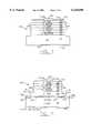
- the double heterostructurewill be incorporated in light emitting diode such as the one broadly designated at 20 in FIG. 1.
- the double heterostructure light emitting diode 20 illustrated in FIG. 1emits in the blue portion of the visible spectrum and comprises a substrate 21 preferably formed of silicon carbide that has been sufficiently doped to provide a conductive substrate for the vertical structure LED 20 illustrated in FIG. 1.
- the silicon carbide substratehas a polytype preferably selected from the group consisting of 6 H or 4 H silicon carbide.
- 4 H and 6 Hare two of the hexagonal crystal forms of silicon carbide, and on which gallium nitride (and other Group III nitrides) form hexagonal polytypes. If cubic (e.g. 3 C) silicon carbide is used as the substrate, however, gallium nitride can also form a cubic structure.
- gallium nitridecan also form a cubic structure.
- the LED 20next includes a buffer layer 22 on the substrate 21.
- a buffer layer 22on the substrate 21.
- Appropriate buffer layersare described in U.S. Pat. No. 5,393,993, and two pending applications, all of which are assigned to the assignee of the present invention and incorporated entirely herein by reference.
- the pending applicationsare Ser. Nos. 08/309,247 and 08/309,251; both filed Sep. 20, 1995 and both to named inventors Edmond et al.
- the buffer structureprovides an appropriate crystal and electronic transition between the silicon carbide substrate and the double heterostructure portion of the LED 20.
- the buffer layercomprises a first layer of gallium nitride and aluminum nitride; and a second layer of gallium nitride and aluminum nitride adjacent to the first layer.
- the mole percentage of aluminum nitride in the second layeris substantially different from the mole percentage of aluminum nitride in the first layer.
- the buffer layercomprises a conductive layer selected from the group consisting of gallium nitride, aluminum nitride, indium nitride, ternary Group III nitrides having the formula A x B 1-x N, where A and B are Group III elements and where x is zero, one, or a fraction between zero and one, quaternary Group III nitrides having the formula A x B y C 1-x-y N where A, B, and C are Group III elements; x and y, are zero, one, or a fraction between zero and one, and 1 is greater than (x+y), and alloys of silicon carbide with such ternary and quaternary Group III nitrides.
- the buffer layercomprises a first layer upon the substrate formed of a graded composition of silicon carbide aluminum gallium nitride in which the portion adjacent the substrate is substantially entirely silicon carbide and the portion furthest from the substrate is substantially entirely aluminum gallium nitride with the portions therebetween being progressively graded in content from predominantly silicon carbide to predominantly aluminum gallium nitride.
- a second layercan be added to the first layer, and can be formed of a graded composition of aluminum gallium nitride.
- the LED 20further comprises an n-type gallium nitride epitaxial layer 23 on the buffer layer 22 which provides an additional crystal transition between the substrate, the buffer, and the heterostructure.
- the LED 20next includes a double heterostructure indicated by the brackets 24 in FIG. 1.
- the double heterostructure 24includes an n-type layer of aluminum gallium nitride 25 which, when the n-type gallium nitride epitaxial layer 23 is included in the structure, rests upon the n-type gallium nitride epitaxial layer 23.
- the n-type layer 25 of aluminum gallium nitridehas the formula Al x Ga 1-x N, where x designates the mole fraction of aluminum, and where 1 is greater than x and x is greater than 0 (1>x>0).
- the mole fraction xis between about 0.05 and 2.0, and in the most preferred embodiments, the mole fraction x is about 0.1.
- the aluminum gallium nitride layer 25furthermore has a net doping density of about 2E18 and is doped with silicon in the most preferred embodiments.
- Eis an abbreviated exponential notation for dopant density, so that 2E18 represents 2 ⁇ 10 18 cm -3 .
- the double heterostructure 24includes an active layer 26 of gallium nitride on the n-type aluminum gallium nitride layer 25 which, as noted above, is compensated with a Group II acceptor and a Group IV donor, and in which the preferred Group II acceptors are zinc or cadmium or magnesium, and in which carbon can comprise a Group IV acceptor.
- the preferred Group IV donoris silicon or germanium. In the most preferred embodiments, the Group II acceptor is zinc, and the Group IV donor is silicon as these produce the characteristic blue emission described herein with respect to a number of the other drawings.
- the net doping density of the active layer 26is between about 1E18 and 4E18, and most preferably about 2E18.
- the double heterostructureis completed with a p-type aluminum gallium nitride layer 27 which has the formula Al x Ga 1-x N where one is greater than x and x is greater than 0 (1>x>0), and in which the preferred mole fraction x is also between about 0.05 and 2.0, and most preferably about 0.1.
- the LED 20can further comprise a p-type gallium nitride layer 30 on the top p-type layer 27 of the heterostructure.
- the p-type layer 27has a net doping density of about 1E19 and is preferably doped with aluminum.
- the LED 20 illustrated in FIG. 1further comprises respective ohmic contacts 31 to the substrate and 32 to the top layer; i.e. to the p-type gallium nitride layer 30 in the embodiment illustrated in FIG. 1. It will be understood, however, that in embodiments that do not include the p-type gallium nitride layer 30, the ohmic layer 32 is made directly to the p-type aluminum gallium nitride layer 27 of the double heterostructure.
- FIG. 1also illustrates that in preferred embodiments, the contact 32 comprises a bonding pad of titanium and gold.
- the contactis formed from a thin layer of titanium (Ti) overlaid with a layer of gold (Au).
- the basic contact 32is accompanied by a transparent ohmic contact 33 which extends across a larger portion of the top surface of the LED 20 to help spread current and thus increase brightness.
- a preferred ohmic contact to the silicon carbide substratecomprises nickel, but can also comprise other appropriate metals or metal combinations such as nickel-vanadium.
- the double heterostructure light emitting diode 20 illustrated in FIG. 1will consistently produce an emission with a peak wavelength of about 430 nanometers (nm) and a bandwidth at half maximum of about 65 nm when a typical LED current (for example between 10 and 40 milliamps) is applied across the p-n junction that is formed by the aluminum gallium nitride layer 27 of the heterostructure and the gallium nitride active layer 26 of the heterostructure 24.
- a typical LED currentfor example between 10 and 40 milliamps
- FIG. 2shows a slightly different embodiment of an LED 40 according to the present invention.
- the substrateis shown at 41
- the buffer layeris shown at 42, but which in this embodiment comprises an insulating buffer layer.
- the buffer layercan comprise the structure disclosed in U.S. Pat. No. 5,393,993.
- the buffer layer 42can comprise a graded layer of AlGaN that is substantially entirely aluminum nitride where it meets the substrate 41, and then is progressively graded with increasing amounts of gallium until it is substantially entirely gallium nitride at its upper surface where it meets the n-type layer of gallium nitride shown as 43 in FIG. 2 and as 23 in FIG. 1.
- the double heterostructureis illustrated at 44 in FIG. 2 and in a preferred embodiment comprises the n-type aluminum gallium nitride layer 45 that otherwise corresponds to the layer 25 described with respect to FIG. 1, a compensated n-type gallium nitride active layer 46 which likewise corresponds to the gallium nitride active layer 26 described with respect to FIG. 1, and a p-type aluminum gallium nitride layer 47 which similarly corresponds to the layer 27 described with respect to FIG. 1.
- a p-type gallium nitride layer 50 corresponding to layer 30 in FIG. 1is on the heterostructure, and the ohmic contacts 51 to the substrate and 52 and 53 to the top of the diode correspond to those described as 31, 32, and 33 in FIG. 1.
- the buffer layer 42 in this embodimentis insulating rather than conductive, some other path for current flow must be provided between the ohmic contact 51 on the substrate and the ohmic contacts 52 and 53 on the top layer of the diode.
- This contactis made through shorting contacts 54 and 55 which are preferably formed on aluminum or titanium and aluminum and which provide an ohmic contact to the n-type gallium nitride layer 43.
- these shorting contactsfurther include portions illustrated at 56 and 57 that are in immediate contact with the n-type silicon carbide substrate and which are formed of titanium and nickel to produce an appropriate ohmic contact with the silicon carbide.
- the inventioncomprises a method of producing an active layer of compensated gallium nitride for a double heterostructure light emitting diode that emits in the blue portion of the visible spectrum.
- the inventioncomprises introducing vaporized sources of gallium, nitrogen, silicon and zinc into a chemical vapor deposition system that includes a semiconductor substrate compatible with the growth of gallium nitride thereon. The temperature is maintained high enough to promote the epitaxial growth of zinc and silicon compensated gallium nitride, but lower than the temperature at which the gallium nitride would decompose.
- the temperaturemust be high enough to provide the energy required to get atoms to move across the epitaxial growth surface, and in preferred embodiments of the present invention, this temperature is generally maintained between about 800° C. and 1050° C.
- the temperatureis preferably maintained lower than the temperature at which the surface morphology of the epitaxial layer would become unacceptable for further epitaxial growth thereon.
- the step of introducing the vaporized source of galliumcomprises introducing trimethyl gallium, (CH 3 ) 3 Ga; the step of introducing a vaporized source of nitrogen comprises introduces ammonia, NH 3 ; the step of introducing a vaporized source of zinc comprises introducing dimethyl zinc, (C 2 H 5 ) 2 Zn; and the step of introducing a vaporized source of silicon comprises introducing silane, SiH 4 .
- the preferred aluminum source(for the AlGaN layers) is trimethyl aluminum, (CH 3 ) 3 Al; and when magnesium is introduced, the preferred source is biscyclopentadienyl magnesium, (C 5 H 5 ) 2 Mg.
- FIG. 3is an SEM photograph of an LED according to the present invention.
- a devicehas a chip size of about 14 mil ⁇ 14 mil, with a 10 mil ⁇ 10 mil mesa portion.
- the substrateis about 7 or 8 mils thick
- the n-GaN layere.g. 23 in FIG. 1 or 43 in FIG. 2 is about 3 microns thick and the layers in the heterostructure (n-AlGaN, GaN, and p-AlGaN are each about 1000 angstroms ( ⁇ ) thick.
- the top GaN layere.g. 30 in FIG. 1 and 50 in FIG. 2) is about 4000 ⁇ thick.
- FIGS. 4-14illustrate various performance characteristics of the layers that make up the heterostructure and heterostructure diode according to the present invention.
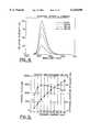
- FIG. 4illustrates the spectral response of a gallium nitride double heterojunction light emitting diode formed on a silicon carbide substrate according to the present invention as a function of operating current.
- FIG. 4shows measurements made at four different currents between 10 and 40 milliamps (mA).
- the peak emission wavelengthis 430 nanometers (nm) with a bandwidth at half maximum of about 60 nanometers which is characteristic of the silicon and zinc compensated gallium nitride active layer.
- FIG. 5illustrates the power output and external quantum efficiency of a light emitting diode according to the present invention as a function of operating current.
- the outputis approximately 850 microwatts which corresponds to an external quantum efficiency of about 1.5%.
- FIG. 6illustrates the room temperature photoluminescence of various combinations of aluminum gallium nitride on silicon carbide substrates and also including a pure gallium nitride layer for comparative purposes.
- the clean, well defined peaks that are measured at room temperaturedemonstrate the high crystal quality of these layers.
- These photoluminescent measurementswere made by exciting the layers with a 10 milliwatt helium/cadmium laser at 325 nanometers.
- FIG. 7demonstrates the current voltage characteristics of ohmic contacts made to n-type gallium nitride on silicon carbide substrates according to the present invention.
- the preferred ohmic contact metalis aluminum which yields a contact resistance of about 10 -5 ohm-cm 2 for an n-type gallium nitride layer with a donor density of about 10 18 cm -3 .
- FIG. 8is a similar current voltage plot demonstrating the characteristics of ohmic contacts made to p-type gallium nitride on silicon carbide substrates according to the present invention.
- the preferred ohmic contact metalis an alloy of titanium and gold which yields a contact resistance of approximately 10 -2 ohms-cm 2 for a p-type acceptor density of approximately 6E17 in the gallium nitride layer.
- FIG. 9is the current voltage (I-V) curve for a gallium nitride double heterojunction light emitting diode on silicon carbide according to the present invention.
- I-Vcurrent voltage
- FIG. 10illustrates the room temperature photoluminescence of magnesium doped p-type gallium nitride on silicon carbide. The peak occurs at about 435 nanometers for a layered doped to a net acceptor concentration of about 6E17.
- FIG. 11is a partial logarithmic plot of Hall effect data showing the carrier concentration and resistivity of an n-type gallium nitride as a function of temperature, plotted inversely to temperature.
- the layer from which the measurements for FIG. 11 were takenwas doped with silicon to a net donor concentration of about 1.4E18 and had a resistivity of 0.016 ohm-centimeter at room temperature.
- FIG. 12is corresponding data for the same layer as illustrated by FIG. 11, but demonstrating mobility for the layer.
- the mobility of the layeris approximately 300 cm 2 /V•s at room temperature, a high value for this doping level indicating the high quality nature of the layer.
- FIG. 13is a plot of Hall effect data showing the acceptor concentration and resistivity of magnesium doped gallium nitride as a function of temperature (plotted inversely). The net acceptor concentration for this layer was about 6E17 and showed a resistivity of about 1.3 ohms-centimeter at room temperature.
- FIG. 14illustrates the corresponding mobility data for the same layer as FIG. 13 and illustrates that the mobility of the layer is approximately 8 cm 2 /V•s at room temperature which is typical of the mobility of p-type gallium nitride.
Landscapes
- Led Devices (AREA)
Abstract
Description
This application is a divisional of Ser. No. 08/436,141 filed May 8, 1995, now U.S. Pat. No. 5,739,554.
The present invention relates to light emitting diodes, and in particular, relates to light emitting diodes formed in semiconductor materials with sufficiently wide band gaps to emit light in the blue portion of the visible spectrum.
A light emitting diode ("LED") is a photonic semiconductor device. Photonic semiconductor devices fall into three categories: devices that convert electrical energy into optical radiation (LED's and diode lasers), devices that detect optical signals (photodetectors), and devices that convert optical radiation into electrical energy (photovoltaic devices or solar cells).
Although all three of these categories or devices have useful applications, the LED may be the most commonly recognized because of its application to such a wide variety of products and applications such as scientific equipment, medical equipment, and perhaps most commonly, various consumer products in which LEDs form the light source for various signals, indicators, gauges, clocks, and many other familiar items.
Semiconductor sources such as LEDs are particularly desirable as light output devices in such items because of their generally long lifetime, their low power requirements, and their high reliability.
In spite of their widespread use, LEDs are to some extent functionally limited, because the color that an LED can produce is fundamentally limited by the nature of semiconductor materials in which the LED is formed. As well known to those of ordinary skill in this and related arts, the light produced by an LED is referred to as "electroluminescence" and represents the generation of light by an electric current passing through a material under an applied electric field. Any given material that produces electroluminescent light tends to do so over a relatively narrow range of wavelengths under given circumstances. Electroluminescence thus differs from thermal radiation or incandescence which generally have much broader spectral widths.
More fundamentally, an LED's luminescence is produced by basic quantum mechanical transitions between energy levels within the semiconductor material. Because the bands within a material depend both upon the material and its doping, the energy of the transition, and thus the color of the radiation it produces, is limited by the well known relationship (E=hv) between the energy (E) of a transition and the frequency (v) of the light it produces (h is Plank's constant). Blue light has a shorter wavelength (and thus a higher frequency) than the other colors in the visible spectrum, and thus must be produced from transitions that are greater in energy than those transitions which produce green, yellow, orange or red light.
More specifically, the entire visible spectrum runs from the violet at about 390 nanometers to the red at about 770 nanometers. In turn, the blue portion of the visible spectrum can be considered (somewhat arbitrarily) to extend between the wavelengths of about 425 and 480 nanometers. The wavelengths of 425 and 480 nanometers in turn represent energy transitions (also somewhat arbitrarily) of about 2.6 eV and about 2.9 eV. Accordingly, only materials with a bandgap of at least about 2.6 eV can produce blue light, even under the best of conditions.
As is further well recognized, blue is one of the primary colors, and thus any devices which hope to produce full color displays using LEDs need to incorporate blue in some fashion. Absent efficient blue LEDs, some other method such as filtering or shuttering must be used to produce a blue contribution to a display that otherwise lacks a blue LED source.
From another standpoint, blue light's shorter wavelength allows it to be used to store more information on optical memory devices (such as CD ROM) than can red or yellow light. In particular, a CD ROM of a given physical size can hold about eight times as much information using blue light than it could when using red light. Thus, the advantages for computer and other sorts of optical memories using blue light are quite attractive.
Candidate materials with sufficient bandgaps to produce blue light include silicon carbide, gallium nitride, other Group III nitrides, zinc sulfide, and zinc selenide. More common semiconductor materials such as silicon, gallium phosphide, or gallium arsenide are unsuitable for producing blue light because their bandgaps are on the order of 2.26 eV or less.
The last decade has seen a great deal of progress in both the basic and commercial development of blue light emitting diodes, including a number of contributions by the assignee of the present invention. These include U.S. Pat. Nos. 4,918,497; 4,966,862; 5,027,168; and 5,338,944.
Another candidate material for blue light emitting diodes is gallium nitride (GaN) and its analogous Group III (i.e. Group III of the periodic table) nitride compounds such as aluminum gallium nitride (AlGaN), indium gallium nitride (InGaN), indium aluminum nitride (InAlN) and in some circumstances indium aluminum gallium nitride (InAlGaN). These materials are particularly attractive because they offer direct energy transitions with bandgaps from between about 3.4 to about 6.2 eV at room temperature. As known to those familiar with LEDs and electronic transitions, a direct (or "vertical") transition occurs in a semiconductor when the valance band maxima and the conduction band minima have the same K value, which in turn means that crystal momentum is conserved during the transition so that the energy produced by the transition can go predominantly into the photon; i.e. to produce light rather than heat. When the conduction and valance band minima are not of the same K value, a phonon (i.e. an emission of vibrational energy) is required to conserve crystal momentum and the transition is called "indirect." The phonon's energy essentially reduces the energy of any resulting photon, thus reducing both the frequency and the intensity of the emitted light. A full discussion of the theory and operation of LEDs is given inChapter 12 of Sze, Physics of Semiconductor Devices, Second Edition (1981), pp. 681ff.
From a more lay point of view, the direct transition characteristics of group III nitrides, including gallium nitride, offer the potential for brighter and more efficient emissions--and thus brighter and more efficient LEDS--than do the emissions from indirect materials such as silicon carbide, all other factors being generally equal.
Accordingly, much interest in the last decade has also focused on producing light emitting diodes in gallium nitride and the related group III nitrides.
Although gallium nitride offers a direct transition over a wide bandgap, and thus a theoretically greater brightness, the material presents a particular set of technical problems in manufacturing working devices. The primary problem is the lack of bulk single crystals of gallium nitride which in turn means that gallium nitride or other group III nitride devices must be formed as epitaxial layers on other materials. The most commonly used material to date has been sapphire (aluminum oxide, Al2 O3). Sapphire offers a reasonable crystal lattice match to Group III nitrides, thermal stability, and transparency, all of which are generally useful in producing a light emitting diode. Sapphire offers the disadvantage, however, of being unsuitable for conductivity doping. In turn, this means that the electric current that must be passed through an LED to generate the emission cannot be directed through the sapphire substrate. Thus other types of connections to the LED must be made. In general, LEDs with "vertical" geometry (i.e. using conductive substrates so that ohmic contacts can be placed at opposite ends of the device) are preferred for a number of reasons, including their easier manufacture than such "nonvertical" devices.
Accordingly, the assignee of the present invention has developed the use of silicon carbide substrates for gallium nitride and other Group III devices as a means of solving the conductivity problems of sapphire as a substrate. Because silicon carbide can be doped conductively, "vertical" LEDs can be formed on it; i.e. devices in which one contact can be made to the top of a device and the second contact to the bottom of the device, a structure which greatly facilitates the manufacture of the LED as well as the incorporation of the LED into circuits or combination devices or structures.
In spite of these theoretical advantages, a consistently reliable and predictable blue emission using a gallium nitride active layer has yet to be accomplished. For example, some workers have used silicon and zinc to co-dope or compensate indium gallium nitride (InGaN) but have interpreted their results to mean that gallium nitride standing alone is not suited as well as InGaN for an LED because InGaN gives a better band-to-band ("interband") transition for a light emitting diode.
Similarly, others have prepared heterojunctions from AlGaN and GaN, but never attempted or described compensated doping, and by all indications, used an intrinsic n-type gallium nitride and p-type AlGaN for the junction. Indeed, if some of the prior art structures are properly understood, doping them with a compensating acceptor such as zinc would have produced an insulating layer rather than a compensated one.
Accordingly, it is an object of the present invention to provide a light emitting diode that takes advantage of gallium nitride's properties, that does so to produce an emission that is both consistent and predictable, and that does so using a compensated active layer.
The invention meets this object with a double heterostructure for a light emitting diode, said heterostructure comprising a layer of aluminum gallium nitride having a first conductivity type; a layer of aluminum gallium nitride having the opposite conductivity type; and a conductive layer of gallium nitride between said aluminum gallium nitride layers, said gallium nitride layer being co-doped with both a Group II acceptor and a Group IV donor, with one of said dopants being present in an amount sufficient to give said gallium nitride layer a net conductivity type, and forming a p-n junction with the adjacent layer of aluminum gallium nitride having the opposite conductivity type therefrom.
In another aspect the invention comprises a double heterostructure light emitting diode that emits in the blue portion of the visible spectrum and comprising a substrate; a buffer layer on said substrate; and the double heterostructure of the invention on the buffer layer.
In yet a third aspect, the invention comprises a method of producing an active layer of compensated n-type gallium nitride for a double heterostructure light emitting diode that emits in the blue portion of the visible spectrum
The foregoing and other objects, advantages and features of the invention, and the manner in which the same are accomplished, will become more readily apparent upon consideration of the following detailed description of the invention taken in conjunction with the accompanying drawings, which illustrate preferred and exemplary embodiments, and wherein:
FIG. 1 is a cross-sectional view of a first embodiment of a light-emitting diode (LED) according to the present invention;
FIG. 2 is a cross-sectional view of a second embodiment of an LED according to the present invention;
FIG. 3 is a scanning electron micrograph of an LED manufactured according to the present invention;
FIG. 4 is a plot of spectral output versus current for an LED according to the present invention;
FIG. 5 is a plot of output and efficiency versus forward current for an LED according to the present invention;
FIG. 6 is a plot of the normalized photoluminescence intensity versus wavelength for aluminum gallium nitride (Alx Ga1-x N);
FIG. 7 is a plot of current versus voltage for ohmic contacts made to n-type gallium nitride on silicon carbide;
FIG. 8 is a plot similar to FIG. 7 except with the ohmic contact made to p-type gallium nitride;
FIG. 9 is a plot of the current-voltage characteristics of an LED according to the present invention;
FIG. 10 is a plot of the room temperature photoluminescence of magnesium doped p-type gallium nitride on silicon carbide;
FIG. 11 is a Hall effect plot demonstrating the carrier concentration and resistivity of the n-type gallium nitride layer as a function of temperature;
FIG. 12 illustrates the mobility data for a silicon doped n-type gallium nitride layer on silicon carbides;
FIG. 13 is another Hall effect plot showing the hole concentration and resistivity of magnesium doped gallium nitride as a function of temperature; and
FIG. 14 is a plot of the mobility data for a magnesium doped p-type gallium nitride layer on silicon carbide.
In its broadest aspect, the invention is a double heterostructure for a light emitting diode comprises a layer of aluminum gallium nitride having a first conductivity type; a layer of aluminum gallium nitride having the opposite conductivity type; and an active layer of gallium nitride between the aluminum gallium nitride layers, in which the gallium nitride layer is co-doped with both a Group II acceptor and a Group IV donor, with one of the dopants being present in an amount sufficient to give the gallium nitride layer a net conductivity type, so that the active layer forms a p-n junction with the adjacent layer of aluminum gallium nitride having the opposite conductivity type.
In a preferred embodiment, the invention is a double heterostructure for a light emitting diode in which the heterostructure comprises a p-type layer of aluminum gallium nitride, an n-type layer of aluminum gallium nitride, and an n-type layer of gallium nitride between the aluminum gallium nitride layers. The gallium nitride layer is codoped with both zinc and silicon and forms a p-n junction with the p-type layer of aluminum gallium nitride.
The double heterostructure offers several advantages over homostructure or single heterostructure devices. These can include enhanced emission based on the different refractive indexes between GaN and AlGaN; more efficient carrier confinement, which in turn leads to more efficient carrier recombination and thus a brighter output in an LED.
In a preferred embodiment, the double heterostructure will be incorporated in light emitting diode such as the one broadly designated at 20 in FIG. 1. The double heterostructurelight emitting diode 20 illustrated in FIG. 1 emits in the blue portion of the visible spectrum and comprises asubstrate 21 preferably formed of silicon carbide that has been sufficiently doped to provide a conductive substrate for thevertical structure LED 20 illustrated in FIG. 1. In order to match the crystal structure of the buffer and aluminum gallium nitride layers on thesubstrate 21, the silicon carbide substrate has a polytype preferably selected from the group consisting of 6 H or 4 H silicon carbide.
As known by those familiar with these materials, 4 H and 6 H are two of the hexagonal crystal forms of silicon carbide, and on which gallium nitride (and other Group III nitrides) form hexagonal polytypes. If cubic (e.g. 3 C) silicon carbide is used as the substrate, however, gallium nitride can also form a cubic structure.
TheLED 20 next includes abuffer layer 22 on thesubstrate 21. Appropriate buffer layers are described in U.S. Pat. No. 5,393,993, and two pending applications, all of which are assigned to the assignee of the present invention and incorporated entirely herein by reference. The pending applications are Ser. Nos. 08/309,247 and 08/309,251; both filed Sep. 20, 1995 and both to named inventors Edmond et al. The buffer structure provides an appropriate crystal and electronic transition between the silicon carbide substrate and the double heterostructure portion of theLED 20.
In one embodiment the buffer layer comprises a first layer of gallium nitride and aluminum nitride; and a second layer of gallium nitride and aluminum nitride adjacent to the first layer. The mole percentage of aluminum nitride in the second layer is substantially different from the mole percentage of aluminum nitride in the first layer.
In another embodiment the buffer layer comprises a conductive layer selected from the group consisting of gallium nitride, aluminum nitride, indium nitride, ternary Group III nitrides having the formula Ax B1-x N, where A and B are Group III elements and where x is zero, one, or a fraction between zero and one, quaternary Group III nitrides having the formula Ax By C1-x-y N where A, B, and C are Group III elements; x and y, are zero, one, or a fraction between zero and one, and 1 is greater than (x+y), and alloys of silicon carbide with such ternary and quaternary Group III nitrides.
In yet another embodiment, the buffer layer comprises a first layer upon the substrate formed of a graded composition of silicon carbide aluminum gallium nitride in which the portion adjacent the substrate is substantially entirely silicon carbide and the portion furthest from the substrate is substantially entirely aluminum gallium nitride with the portions therebetween being progressively graded in content from predominantly silicon carbide to predominantly aluminum gallium nitride. A second layer can be added to the first layer, and can be formed of a graded composition of aluminum gallium nitride.
In preferred embodiments, theLED 20 further comprises an n-type galliumnitride epitaxial layer 23 on thebuffer layer 22 which provides an additional crystal transition between the substrate, the buffer, and the heterostructure.
TheLED 20 next includes a double heterostructure indicated by thebrackets 24 in FIG. 1. Thedouble heterostructure 24 includes an n-type layer ofaluminum gallium nitride 25 which, when the n-type galliumnitride epitaxial layer 23 is included in the structure, rests upon the n-type galliumnitride epitaxial layer 23. The n-type layer 25 of aluminum gallium nitride has the formula Alx Ga1-x N, where x designates the mole fraction of aluminum, and where 1 is greater than x and x is greater than 0 (1>x>0). In preferred embodiments the mole fraction x is between about 0.05 and 2.0, and in the most preferred embodiments, the mole fraction x is about 0.1. The aluminumgallium nitride layer 25 furthermore has a net doping density of about 2E18 and is doped with silicon in the most preferred embodiments. As commonly used in this art, "E", is an abbreviated exponential notation for dopant density, so that 2E18 represents 2×1018 cm-3.
Thedouble heterostructure 24 includes anactive layer 26 of gallium nitride on the n-type aluminumgallium nitride layer 25 which, as noted above, is compensated with a Group II acceptor and a Group IV donor, and in which the preferred Group II acceptors are zinc or cadmium or magnesium, and in which carbon can comprise a Group IV acceptor. The preferred Group IV donor is silicon or germanium. In the most preferred embodiments, the Group II acceptor is zinc, and the Group IV donor is silicon as these produce the characteristic blue emission described herein with respect to a number of the other drawings. The net doping density of theactive layer 26 is between about 1E18 and 4E18, and most preferably about 2E18.
The double heterostructure is completed with a p-type aluminumgallium nitride layer 27 which has the formula Alx Ga1-x N where one is greater than x and x is greater than 0 (1>x>0), and in which the preferred mole fraction x is also between about 0.05 and 2.0, and most preferably about 0.1.
In preferred embodiments, theLED 20 can further comprise a p-typegallium nitride layer 30 on the top p-type layer 27 of the heterostructure. The p-type layer 27 has a net doping density of about 1E19 and is preferably doped with aluminum.
TheLED 20 illustrated in FIG. 1 further comprises respectiveohmic contacts 31 to the substrate and 32 to the top layer; i.e. to the p-typegallium nitride layer 30 in the embodiment illustrated in FIG. 1. It will be understood, however, that in embodiments that do not include the p-typegallium nitride layer 30, theohmic layer 32 is made directly to the p-type aluminumgallium nitride layer 27 of the double heterostructure.
FIG. 1 also illustrates that in preferred embodiments, thecontact 32 comprises a bonding pad of titanium and gold. In a most preferred embodiment, the contact is formed from a thin layer of titanium (Ti) overlaid with a layer of gold (Au). In a preferred embodiment, thebasic contact 32 is accompanied by a transparentohmic contact 33 which extends across a larger portion of the top surface of theLED 20 to help spread current and thus increase brightness.
A preferred ohmic contact to the silicon carbide substrate comprises nickel, but can also comprise other appropriate metals or metal combinations such as nickel-vanadium.
The double heterostructurelight emitting diode 20 illustrated in FIG. 1 will consistently produce an emission with a peak wavelength of about 430 nanometers (nm) and a bandwidth at half maximum of about 65 nm when a typical LED current (for example between 10 and 40 milliamps) is applied across the p-n junction that is formed by the aluminumgallium nitride layer 27 of the heterostructure and the gallium nitrideactive layer 26 of theheterostructure 24.
FIG. 2 shows a slightly different embodiment of anLED 40 according to the present invention. In FIG. 2, the substrate is shown at 41, and the buffer layer is shown at 42, but which in this embodiment comprises an insulating buffer layer. As noted earlier herein, the buffer layer can comprise the structure disclosed in U.S. Pat. No. 5,393,993. Alternatively, thebuffer layer 42 can comprise a graded layer of AlGaN that is substantially entirely aluminum nitride where it meets thesubstrate 41, and then is progressively graded with increasing amounts of gallium until it is substantially entirely gallium nitride at its upper surface where it meets the n-type layer of gallium nitride shown as 43 in FIG. 2 and as 23 in FIG. 1.
The double heterostructure is illustrated at 44 in FIG. 2 and in a preferred embodiment comprises the n-type aluminumgallium nitride layer 45 that otherwise corresponds to thelayer 25 described with respect to FIG. 1, a compensated n-type gallium nitrideactive layer 46 which likewise corresponds to the gallium nitrideactive layer 26 described with respect to FIG. 1, and a p-type aluminumgallium nitride layer 47 which similarly corresponds to thelayer 27 described with respect to FIG. 1. A p-typegallium nitride layer 50 corresponding to layer 30 in FIG. 1 is on the heterostructure, and theohmic contacts 51 to the substrate and 52 and 53 to the top of the diode correspond to those described as 31, 32, and 33 in FIG. 1.
As FIG. 2 illustrates, however, because thebuffer layer 42 in this embodiment is insulating rather than conductive, some other path for current flow must be provided between theohmic contact 51 on the substrate and theohmic contacts contacts gallium nitride layer 43. In the most preferred embodiments, these shorting contacts further include portions illustrated at 56 and 57 that are in immediate contact with the n-type silicon carbide substrate and which are formed of titanium and nickel to produce an appropriate ohmic contact with the silicon carbide.
In another aspect, the invention comprises a method of producing an active layer of compensated gallium nitride for a double heterostructure light emitting diode that emits in the blue portion of the visible spectrum. In this aspect, the invention comprises introducing vaporized sources of gallium, nitrogen, silicon and zinc into a chemical vapor deposition system that includes a semiconductor substrate compatible with the growth of gallium nitride thereon. The temperature is maintained high enough to promote the epitaxial growth of zinc and silicon compensated gallium nitride, but lower than the temperature at which the gallium nitride would decompose. As is well understood by those of ordinary skill in this art, the temperature must be high enough to provide the energy required to get atoms to move across the epitaxial growth surface, and in preferred embodiments of the present invention, this temperature is generally maintained between about 800° C. and 1050° C.
It will be further understood by those of ordinary skill in this art, that gas flow rates and specific temperatures are generally system-dependent, and thus specific temperatures and the like other than those recited herein will fall within the method aspects of the invention because they can be easily determined for particular chemical vapor deposition ("CVD") systems by those of ordinary skill in this art and without undue experimentation.
As another limiting factor, the temperature is preferably maintained lower than the temperature at which the surface morphology of the epitaxial layer would become unacceptable for further epitaxial growth thereon.
In preferred embodiments, the step of introducing the vaporized source of gallium comprises introducing trimethyl gallium, (CH3)3 Ga; the step of introducing a vaporized source of nitrogen comprises introduces ammonia, NH3 ; the step of introducing a vaporized source of zinc comprises introducing dimethyl zinc, (C2 H5)2 Zn; and the step of introducing a vaporized source of silicon comprises introducing silane, SiH4. The preferred aluminum source (for the AlGaN layers) is trimethyl aluminum, (CH3)3 Al; and when magnesium is introduced, the preferred source is biscyclopentadienyl magnesium, (C5 H5)2 Mg.
FIG. 3 is an SEM photograph of an LED according to the present invention. Such a device has a chip size of about 14 mil×14 mil, with a 10 mil×10 mil mesa portion. The substrate is about 7 or 8 mils thick, the n-GaN layer (e.g. 23 in FIG. 1 or 43 in FIG. 2) is about 3 microns thick and the layers in the heterostructure (n-AlGaN, GaN, and p-AlGaN are each about 1000 angstroms (Å) thick. The top GaN layer (e.g. 30 in FIG. 1 and 50 in FIG. 2) is about 4000 Å thick.
FIGS. 4-14 illustrate various performance characteristics of the layers that make up the heterostructure and heterostructure diode according to the present invention. FIG. 4 illustrates the spectral response of a gallium nitride double heterojunction light emitting diode formed on a silicon carbide substrate according to the present invention as a function of operating current. FIG. 4 shows measurements made at four different currents between 10 and 40 milliamps (mA). The peak emission wavelength is 430 nanometers (nm) with a bandwidth at half maximum of about 60 nanometers which is characteristic of the silicon and zinc compensated gallium nitride active layer.
FIG. 5 illustrates the power output and external quantum efficiency of a light emitting diode according to the present invention as a function of operating current. As a normal operating current for such an LED (i.e. approximately 20 milliamps), the output is approximately 850 microwatts which corresponds to an external quantum efficiency of about 1.5%.
FIG. 6 illustrates the room temperature photoluminescence of various combinations of aluminum gallium nitride on silicon carbide substrates and also including a pure gallium nitride layer for comparative purposes. The clean, well defined peaks that are measured at room temperature demonstrate the high crystal quality of these layers. These photoluminescent measurements were made by exciting the layers with a 10 milliwatt helium/cadmium laser at 325 nanometers.
FIG. 7 demonstrates the current voltage characteristics of ohmic contacts made to n-type gallium nitride on silicon carbide substrates according to the present invention. The preferred ohmic contact metal is aluminum which yields a contact resistance of about 10-5 ohm-cm2 for an n-type gallium nitride layer with a donor density of about 1018 cm-3.
FIG. 8 is a similar current voltage plot demonstrating the characteristics of ohmic contacts made to p-type gallium nitride on silicon carbide substrates according to the present invention. The preferred ohmic contact metal is an alloy of titanium and gold which yields a contact resistance of approximately 10-2 ohms-cm2 for a p-type acceptor density of approximately 6E17 in the gallium nitride layer.
FIG. 9 is the current voltage (I-V) curve for a gallium nitride double heterojunction light emitting diode on silicon carbide according to the present invention. In reverse bias no leakage current is detected. Under forward bias the LED begins to turn on at about 2.7 volts and exhibits an operating voltage of about 3.7 volts at a typical current of 20 milliamps.
FIG. 10 illustrates the room temperature photoluminescence of magnesium doped p-type gallium nitride on silicon carbide. The peak occurs at about 435 nanometers for a layered doped to a net acceptor concentration of about 6E17.
FIG. 11 is a partial logarithmic plot of Hall effect data showing the carrier concentration and resistivity of an n-type gallium nitride as a function of temperature, plotted inversely to temperature. The layer from which the measurements for FIG. 11 were taken was doped with silicon to a net donor concentration of about 1.4E18 and had a resistivity of 0.016 ohm-centimeter at room temperature.
FIG. 12 is corresponding data for the same layer as illustrated by FIG. 11, but demonstrating mobility for the layer. The mobility of the layer is approximately 300 cm2 /V•s at room temperature, a high value for this doping level indicating the high quality nature of the layer.
FIG. 13 is a plot of Hall effect data showing the acceptor concentration and resistivity of magnesium doped gallium nitride as a function of temperature (plotted inversely). The net acceptor concentration for this layer was about 6E17 and showed a resistivity of about 1.3 ohms-centimeter at room temperature.
FIG. 14 illustrates the corresponding mobility data for the same layer as FIG. 13 and illustrates that the mobility of the layer is approximately 8 cm2 /V•s at room temperature which is typical of the mobility of p-type gallium nitride.
In the drawings and specification, there have been disclosed typical preferred embodiments of the invention and, although specific terms have been employed, they have been used in a generic and descriptive sense only and not for purposes of limitation, the scope of the invention being set forth in the following claims.
Claims (7)
1. A method of producing an active layer of zinc and silicon compensated n-type gallium nitride for a double heterostructure light emitting diode that emits in the blue portion of the visible spectrum, the method comprising:
introducing vaporized sources of gallium, nitrogen, silicon and zinc into a chemical vapor deposition system that includes a semiconductor substrate compatible with the growth of gallium nitride thereon; and while
maintaining the temperature high enough to promote the epitaxial growth of zinc and silicon compensated gallium nitride, but lower than the temperature at which the gallium nitride would decompose.
2. A method according to claim 1 wherein the temperature is maintained lower than the temperature at which the surface morphology of the epitaxial layer would become unacceptable for further epitaxial growth thereon.
3. A method according to claim 1 wherein the temperature is maintained between about 800° C. and 1050° C.
4. A method according to claim 1 wherein the step of introducing a vaporized source of gallium comprises introducing trimethyl gallium.
5. A method according to claim 1 wherein the step of introducing a vaporized source of nitrogen comprises introducing ammonia.
6. A method according to claim 1 wherein the step of introducing a vaporized source of zinc comprises introducing diethyl zinc.
7. A method according to claim 1 wherein the step of introducing a vaporized source of silicon comprises introducing silane.
Priority Applications (1)
| Application Number | Priority Date | Filing Date | Title |
|---|---|---|---|
| US09/059,649US6120600A (en) | 1995-05-08 | 1998-04-13 | Double heterojunction light emitting diode with gallium nitride active layer |
Applications Claiming Priority (2)
| Application Number | Priority Date | Filing Date | Title |
|---|---|---|---|
| US08/436,141US5739554A (en) | 1995-05-08 | 1995-05-08 | Double heterojunction light emitting diode with gallium nitride active layer |
| US09/059,649US6120600A (en) | 1995-05-08 | 1998-04-13 | Double heterojunction light emitting diode with gallium nitride active layer |
Related Parent Applications (1)
| Application Number | Title | Priority Date | Filing Date |
|---|---|---|---|
| US08/436,141DivisionUS5739554A (en) | 1995-05-08 | 1995-05-08 | Double heterojunction light emitting diode with gallium nitride active layer |
Publications (1)
| Publication Number | Publication Date |
|---|---|
| US6120600Atrue US6120600A (en) | 2000-09-19 |
Family
ID=23731271
Family Applications (2)
| Application Number | Title | Priority Date | Filing Date |
|---|---|---|---|
| US08/436,141Expired - LifetimeUS5739554A (en) | 1995-05-08 | 1995-05-08 | Double heterojunction light emitting diode with gallium nitride active layer |
| US09/059,649Expired - LifetimeUS6120600A (en) | 1995-05-08 | 1998-04-13 | Double heterojunction light emitting diode with gallium nitride active layer |
Family Applications Before (1)
| Application Number | Title | Priority Date | Filing Date |
|---|---|---|---|
| US08/436,141Expired - LifetimeUS5739554A (en) | 1995-05-08 | 1995-05-08 | Double heterojunction light emitting diode with gallium nitride active layer |
Country Status (9)
| Country | Link |
|---|---|
| US (2) | US5739554A (en) |
| EP (1) | EP0826246A1 (en) |
| JP (1) | JPH11504764A (en) |
| KR (1) | KR19990008420A (en) |
| CN (1) | CN1156028C (en) |
| AU (1) | AU5545296A (en) |
| CA (1) | CA2220031C (en) |
| TW (1) | TW362291B (en) |
| WO (1) | WO1996036080A1 (en) |
Cited By (230)
| Publication number | Priority date | Publication date | Assignee | Title |
|---|---|---|---|---|
| US6235017B1 (en)* | 1997-03-11 | 2001-05-22 | Vitcon Projektconsult Gmbh | Device for ablation of material by means of laser radiation |
| US6407411B1 (en) | 2000-04-13 | 2002-06-18 | General Electric Company | Led lead frame assembly |
| US20030080344A1 (en)* | 2001-10-26 | 2003-05-01 | Yoo Myung Cheol | Diode having vertical structure and method of manufacturing the same |
| US20030087461A1 (en)* | 2001-11-06 | 2003-05-08 | Stokes Edward Brittain | Methods and apparatus for a semiconductor device |
| US20030090103A1 (en)* | 2001-11-09 | 2003-05-15 | Thomas Becker | Direct mailing device |
| US6617060B2 (en) | 2000-12-14 | 2003-09-09 | Nitronex Corporation | Gallium nitride materials and methods |
| US20030189212A1 (en)* | 2002-04-09 | 2003-10-09 | Yoo Myung Cheol | Method of fabricating vertical devices using a metal support film |
| US20040016929A1 (en)* | 2001-09-06 | 2004-01-29 | Osamu Nakatsuka | Electrode for p-type sic |
| US20040031956A1 (en)* | 2002-08-16 | 2004-02-19 | Saxler Adam William | Heterogeneous bandgap structures for semiconductor devices and manufacturing methods therefor |
| US20040033638A1 (en)* | 2000-10-17 | 2004-02-19 | Stefan Bader | Method for fabricating a semiconductor component based on GaN |
| US20040056260A1 (en)* | 2002-09-19 | 2004-03-25 | Slater David B. | Phosphor-coated light emitting diodes including tapered sidewalls, and fabrication methods therefor |
| US20040057482A1 (en)* | 2002-09-25 | 2004-03-25 | Cao Group, Inc. | GaN structures having low dislocation density and methods of manufacture |
| US20040061433A1 (en)* | 2001-10-12 | 2004-04-01 | Nichia Corporation, Corporation Of Japan | Light emitting apparatus and method of manufacturing the same |
| US20040075399A1 (en)* | 2002-10-22 | 2004-04-22 | Hall David Charles | LED light engine for AC operation and methods of fabricating same |
| US6740906B2 (en) | 2001-07-23 | 2004-05-25 | Cree, Inc. | Light emitting diodes including modifications for submount bonding |
| US20040124429A1 (en)* | 2002-12-31 | 2004-07-01 | Edward Stokes | Layered phosphor coatings for led devices |
| US20040130002A1 (en)* | 2001-02-23 | 2004-07-08 | Nitronex Corporation | Gallium nitride material devices and methods of forming the same |
| US20040147054A1 (en)* | 2002-12-20 | 2004-07-29 | Haberern Kevin Ward | Methods of forming semiconductor devices including mesa structures and multiple passivation layers and related devices |
| US20040149993A1 (en)* | 2003-01-30 | 2004-08-05 | Cree, Inc. | Methods of Treating a Silicon Carbide Substrate for Improved Epitaxial Deposition and Resulting Structures and Devices |
| US20040159849A1 (en)* | 2003-02-14 | 2004-08-19 | Cree, Inc. | Light emitting device incorporating a luminescent material |
| US6791119B2 (en) | 2001-02-01 | 2004-09-14 | Cree, Inc. | Light emitting diodes including modifications for light extraction |
| US20040178417A1 (en)* | 2003-03-10 | 2004-09-16 | Andrews Peter S. | Light emitting devices for light conversion and methods and semiconductor chips for fabricating the same |
| US6794684B2 (en) | 2001-02-01 | 2004-09-21 | Cree, Inc. | Reflective ohmic contacts for silicon carbide including a layer consisting essentially of nickel, methods of fabricating same, and light emitting devices including the same |
| US20040200882A1 (en)* | 2001-07-23 | 2004-10-14 | Slater David B. | Bonding of light emitting diodes having shaped substrates |
| US20040217370A1 (en)* | 2003-04-30 | 2004-11-04 | Negley Gerald H. | Light-emitting devices having an antireflective layer that has a graded index of refraction and methods of forming the same |
| US20040217360A1 (en)* | 2003-04-30 | 2004-11-04 | Negley Gerald H. | Light-emitting devices having coplanar electrical contacts adjacent to a substrate surface opposite an active region and methods of forming the same |
| US20040217361A1 (en)* | 2003-04-30 | 2004-11-04 | Negley Gerald H. | Light-emitting devices having an active region with electrical contacts coupled to opposing surfaces thereof and methods of forming the same |
| US20050045906A1 (en)* | 2003-09-03 | 2005-03-03 | Chuan-Cheng Tu | Light emitting device |
| US20050051789A1 (en)* | 2003-09-09 | 2005-03-10 | Negley Gerald H. | Solid metal block mounting substrates for semiconductor light emitting devices, and oxidizing methods for fabricating same |
| US20050051782A1 (en)* | 2003-09-09 | 2005-03-10 | Negley Gerald H. | Transmissive optical elements including transparent plastic shell having a phosphor dispersed therein, and methods of fabricating same |
| US20050062140A1 (en)* | 2003-09-18 | 2005-03-24 | Cree, Inc. | Molded chip fabrication method and apparatus |
| US20050093004A1 (en)* | 2002-06-26 | 2005-05-05 | Yoo Myung C. | Thin film light emitting diode |
| US20050098792A1 (en)* | 2002-04-09 | 2005-05-12 | Jong-Lam Lee | Method of fabricating vertical structure LEDs |
| US20050121686A1 (en)* | 2003-12-09 | 2005-06-09 | Bernd Keller | Semiconductor light emitting devices and submounts and methods for forming the same |
| US20050133818A1 (en)* | 2003-12-17 | 2005-06-23 | Johnson Jerry W. | Gallium nitride material devices including an electrode-defining layer and methods of forming the same |
| US20050145851A1 (en)* | 2003-12-17 | 2005-07-07 | Nitronex Corporation | Gallium nitride material structures including isolation regions and methods |
| US20050151138A1 (en)* | 2003-11-12 | 2005-07-14 | Slater David B.Jr. | Methods of processing semiconductor wafer backsides having light emitting devices (LEDS) thereon and leds so formed |
| US20050167775A1 (en)* | 2003-08-05 | 2005-08-04 | Nitronex Corporation | Gallium nitride material transistors and methods associated with the same |
| US20050215000A1 (en)* | 2004-03-26 | 2005-09-29 | Negley Gerald H | Etching of substrates of light emitting devices |
| US20050211999A1 (en)* | 2004-03-29 | 2005-09-29 | Negley Gerald H | Doping of gallium nitride by solid source diffusion and resulting gallium nitride structures |
| US20050221519A1 (en)* | 2004-03-31 | 2005-10-06 | Michael Leung | Semiconductor light emitting devices including a luminescent conversion element and methods for packaging the same |
| US20050218421A1 (en)* | 2004-03-31 | 2005-10-06 | Peter Andrews | Methods for packaging a light emitting device and packaged light emitting devices |
| US20050221518A1 (en)* | 2004-03-31 | 2005-10-06 | Peter Andrews | Reflector packages and methods for packaging of a semiconductor light emitting device |
| US20050227379A1 (en)* | 2004-04-01 | 2005-10-13 | Matthew Donofrio | Laser patterning of light emitting devices and patterned light emitting devices |
| US20050224829A1 (en)* | 2004-04-06 | 2005-10-13 | Negley Gerald H | Light-emitting devices having multiple encapsulation layers with at least one of the encapsulation layers including nanoparticles and methods of forming the same |
| US20050285141A1 (en)* | 2004-06-28 | 2005-12-29 | Piner Edwin L | Gallium nitride materials and methods associated with the same |
| US20050285155A1 (en)* | 2004-06-28 | 2005-12-29 | Nitronex Corporation | Semiconductor device-based sensors and methods associated with the same |
| US20060002442A1 (en)* | 2004-06-30 | 2006-01-05 | Kevin Haberern | Light emitting devices having current blocking structures and methods of fabricating light emitting devices having current blocking structures |
| US6984840B2 (en)* | 1998-05-18 | 2006-01-10 | Fujitsu Limited | Optical semiconductor device having an epitaxial layer of III-V compound semiconductor material containing N as a group V element |
| US20060006404A1 (en)* | 2004-06-30 | 2006-01-12 | James Ibbetson | Chip-scale methods for packaging light emitting devices and chip-scale packaged light emitting devices |
| US20060006500A1 (en)* | 2004-07-07 | 2006-01-12 | Nitronex Corporation | III-nitride materials including low dislocation densities and methods associated with the same |
| US20060018122A1 (en)* | 2004-07-23 | 2006-01-26 | Negley Gerald H | Reflective optical elements for semiconductor light emitting devices |
| US20060022209A1 (en)* | 2004-07-27 | 2006-02-02 | Kevin Haberern | Light emitting devices having a reflective bond pad and methods of fabricating light emitting devices having reflective bond pads |
| US20060046328A1 (en)* | 2004-07-27 | 2006-03-02 | Mark Raffetto | Ultra-thin ohmic contacts for p-type nitride light emitting devices and methods of forming |
| US20060060872A1 (en)* | 2004-09-22 | 2006-03-23 | Edmond John A | High output group III nitride light emitting diodes |
| US20060060877A1 (en)* | 2004-09-22 | 2006-03-23 | Edmond John A | High efficiency group III nitride-silicon carbide light emitting diode |
| US20060060874A1 (en)* | 2004-09-22 | 2006-03-23 | Edmond John A | High efficiency group III nitride LED with lenticular surface |
| US20060060879A1 (en)* | 2004-09-22 | 2006-03-23 | Edmond John A | High ouput small area group III nitride leds |
| US20060063289A1 (en)* | 2004-09-21 | 2006-03-23 | Negley Gerald H | Methods of coating semiconductor light emitting elements by evaporating solvent from a suspension |
| WO2006036251A1 (en) | 2004-09-23 | 2006-04-06 | Cree, Inc. | Semiconductor light emitting devices including patternable films comprising transparent silicone and phosphor, and methods of manufacturing same |
| US20060097385A1 (en)* | 2004-10-25 | 2006-05-11 | Negley Gerald H | Solid metal block semiconductor light emitting device mounting substrates and packages including cavities and heat sinks, and methods of packaging same |
| US20060128118A1 (en)* | 2002-07-08 | 2006-06-15 | Nichia Corporation | Nitride semiconductor device comprising bonded substrate and fabrication method of the same |
| US20060138937A1 (en)* | 2004-12-28 | 2006-06-29 | James Ibbetson | High efficacy white LED |
| US20060139945A1 (en)* | 2004-12-23 | 2006-06-29 | Negley Gerald H | Light emitting diode arrays for direct backlighting of liquid crystal displays |
| US20060152651A1 (en)* | 2005-01-12 | 2006-07-13 | Negley Gerald H | Solid colloidal dispersions for backlighting of liquid crystal displays |
| US20060214289A1 (en)* | 2004-10-28 | 2006-09-28 | Nitronex Corporation | Gallium nitride material-based monolithic microwave integrated circuits |
| US20060249748A1 (en)* | 2005-05-03 | 2006-11-09 | Nitronex Corporation | Gallium nitride material structures including substrates and methods associated with the same |
| US20060267043A1 (en)* | 2005-05-27 | 2006-11-30 | Emerson David T | Deep ultraviolet light emitting devices and methods of fabricating deep ultraviolet light emitting devices |
| USD536308S1 (en)* | 2004-10-19 | 2007-02-06 | Rohm Co., Ltd. | Light emitting diode |
| US20070029569A1 (en)* | 2005-08-04 | 2007-02-08 | Peter Andrews | Packages for semiconductor light emitting devices utilizing dispensed encapsulants and methods of packaging the same |
| USD539240S1 (en)* | 2004-10-19 | 2007-03-27 | Rohm Co., Ltd. | Light emitting diode |
| US7211833B2 (en) | 2001-07-23 | 2007-05-01 | Cree, Inc. | Light emitting diodes including barrier layers/sublayers |
| US20070164454A1 (en)* | 2006-01-19 | 2007-07-19 | Cree, Inc. | Dispensed electrical interconnections |
| US7247889B2 (en) | 2004-12-03 | 2007-07-24 | Nitronex Corporation | III-nitride material structures including silicon substrates |
| US20070170454A1 (en)* | 2006-01-20 | 2007-07-26 | Cree, Inc. | Packages for semiconductor light emitting devices utilizing dispensed reflectors and methods of forming the same |
| US20070202360A1 (en)* | 2005-10-04 | 2007-08-30 | Nitronex Corporation | Gallium nitride material transistors and methods for wideband applications |
| US20070228387A1 (en)* | 2006-04-04 | 2007-10-04 | Gerald Negley | Uniform emission LED package |
| US20070235745A1 (en)* | 2006-04-11 | 2007-10-11 | Nissan Motor Co., Ltd. | Semiconductor device and manufacturing method thereof |
| US20070274063A1 (en)* | 2006-05-23 | 2007-11-29 | Led Lighting Fixtures, Inc. | Lighting device and method of making |
| US20070272957A1 (en)* | 2005-12-02 | 2007-11-29 | Nitronex Corporation | Gallium nitride material devices and associated methods |
| US20070278512A1 (en)* | 2006-05-31 | 2007-12-06 | Cree, Inc. | Packaged light emitting devices including multiple index lenses and methods of fabricating the same |
| US20080035143A1 (en)* | 2006-08-14 | 2008-02-14 | Sievers Robert E | Human-powered dry powder inhaler and dry powder inhaler compositions |
| US20080042141A1 (en)* | 2006-08-18 | 2008-02-21 | Adam William Saxler | Structure and method for reducing forward voltage across a silicon carbide-group iii nitride interface |
| US20080044934A1 (en)* | 2006-08-21 | 2008-02-21 | Loh Ban P | Methods of forming semiconductor light emitting device packages by liquid injection molding and molded semiconductor light emitting device strips |
| US20080054286A1 (en)* | 2005-01-27 | 2008-03-06 | Cree, Inc. | Light emitting device packages, light emitting diode (LED) packages and related methods |
| US20080061311A1 (en)* | 2005-01-24 | 2008-03-13 | Cree, Inc. | Led with current confinement structure and surface roughening |
| US20080079017A1 (en)* | 2006-07-31 | 2008-04-03 | Cree, Inc. | Method of uniform phosphor chip coating and led package fabricated using method |
| US7355284B2 (en) | 2004-03-29 | 2008-04-08 | Cree, Inc. | Semiconductor light emitting devices including flexible film having therein an optical element |
| US20080102610A1 (en)* | 2000-08-04 | 2008-05-01 | The Regents Of The University Of California | Method of controlling stress in gallium nitride films deposited on substrates |
| US20080099770A1 (en)* | 2006-10-31 | 2008-05-01 | Medendorp Nicholas W | Integrated heat spreaders for light emitting devices (LEDs) and related assemblies |
| US20080142817A1 (en)* | 2005-06-30 | 2008-06-19 | Cree, Inc. | Chip-scale methods for packaging light emitting devices and chip-scale packaged light emitting devices |
| US20080170396A1 (en)* | 2006-11-09 | 2008-07-17 | Cree, Inc. | LED array and method for fabricating same |
| US20080173884A1 (en)* | 2007-01-22 | 2008-07-24 | Cree, Inc. | Wafer level phosphor coating method and devices fabricated utilizing method |
| US20080194061A1 (en)* | 2007-02-12 | 2008-08-14 | Medendorp Nicholas W | Methods of forming packaged semiconductor light emitting devices having multiple optical elements by compression molding |
| US20080191225A1 (en)* | 2007-02-12 | 2008-08-14 | Medendorp Nicholas W | Methods of forming packaged semiconductor light emitting devices having front contacts by compression molding |
| US20080198572A1 (en)* | 2007-02-21 | 2008-08-21 | Medendorp Nicholas W | LED lighting systems including luminescent layers on remote reflectors |
| US20080272383A1 (en)* | 2007-05-04 | 2008-11-06 | Loh Ban P | Side mountable semiconductor light emitting device packages, panels and methods of forming the same |
| DE102008021572A1 (en) | 2007-05-02 | 2008-12-11 | Cree, Inc. | Multichip LED lights |
| US20090002979A1 (en)* | 2007-06-27 | 2009-01-01 | Cree, Inc. | Light emitting device (led) lighting systems for emitting light in multiple directions and related methods |
| US20090002986A1 (en)* | 2007-06-27 | 2009-01-01 | Cree, Inc. | Light Emitting Device (LED) Lighting Systems for Emitting Light in Multiple Directions and Related Methods |
| US20090014736A1 (en)* | 2007-07-11 | 2009-01-15 | Cree, Inc. | Coating method utilizing phosphor containment structure and devices fabricated using same |
| US20090057690A1 (en)* | 2007-01-22 | 2009-03-05 | Cree, Inc. | Wafer level phosphor coating technique for warm light emitting diodes |
| US20090108269A1 (en)* | 2007-10-26 | 2009-04-30 | Led Lighting Fixtures, Inc. | Illumination device having one or more lumiphors, and methods of fabricating same |
| US20090121615A1 (en)* | 2007-11-14 | 2009-05-14 | Cree, Inc. | Cerium and Europium Doped Phosphor Compositions and Light Emitting Devices Including the Same |
| US20090153022A1 (en)* | 2007-12-14 | 2009-06-18 | Hussell Christopher P | Phosphor distribution in LED lamps using centrifugal force |
| US7566913B2 (en) | 2005-12-02 | 2009-07-28 | Nitronex Corporation | Gallium nitride material devices including conductive regions and methods associated with the same |
| US20090194775A1 (en)* | 2008-02-01 | 2009-08-06 | Cree, Inc. | Semiconductor light emitting devices with high color rendering |
| US20090194773A1 (en)* | 2008-02-05 | 2009-08-06 | Nitronex Corporation | Gallium nitride material devices including diamond regions and methods associated with the same |
| US20090236621A1 (en)* | 2008-03-19 | 2009-09-24 | Cree, Inc. | Low index spacer layer in LED devices |
| US20090267188A1 (en)* | 2008-04-29 | 2009-10-29 | Nitronex Corporation | Gallium nitride material processing and related device structures |
| US7614759B2 (en) | 2005-12-22 | 2009-11-10 | Cree Led Lighting Solutions, Inc. | Lighting device |
| US20090315061A1 (en)* | 2008-06-24 | 2009-12-24 | Cree, Inc. | Methods of assembly for a semiconductor light emitting device package |
| US20100081218A1 (en)* | 2008-09-26 | 2010-04-01 | Craig Hardin | Forming Light Emitting Devices Including Custom Wavelength Conversion Structures |
| US20100155763A1 (en)* | 2008-01-15 | 2010-06-24 | Cree, Inc. | Systems and methods for application of optical materials to optical elements |
| US7745848B1 (en) | 2007-08-15 | 2010-06-29 | Nitronex Corporation | Gallium nitride material devices and thermal designs thereof |
| US20100212048A1 (en)* | 2004-02-12 | 2010-08-19 | Jacobus Gerardus Joannes Hoogstraten | Methods for coupling resistance alleles in tomato |
| US7795623B2 (en) | 2004-06-30 | 2010-09-14 | Cree, Inc. | Light emitting devices having current reducing structures and methods of forming light emitting devices having current reducing structures |
| EP2262017A2 (en) | 2001-07-23 | 2010-12-15 | Cree, Inc. | Flip-Chip bonding of light emitting devices and light emitting devices suitable for Flip-Chip bonding |
| US7858403B2 (en) | 2001-10-31 | 2010-12-28 | Cree, Inc. | Methods and systems for fabricating broad spectrum light emitting devices |
| DE112004000136B4 (en)* | 2003-01-17 | 2010-12-30 | Sanken Electric Co. Ltd., Niiza-shi | Semiconductor devices |
| US7863635B2 (en) | 2007-08-07 | 2011-01-04 | Cree, Inc. | Semiconductor light emitting devices with applied wavelength conversion materials |
| WO2011008627A2 (en) | 2009-07-15 | 2011-01-20 | Cree, Inc. | Single-color wavelength-converted light emitting devices |
| US20110193118A1 (en)* | 2010-02-09 | 2011-08-11 | Oshima Yukitoyo | Light emitting device and manufacturing method thereof |
| US8008676B2 (en) | 2006-05-26 | 2011-08-30 | Cree, Inc. | Solid state light emitting device and method of making same |
| US8033692B2 (en) | 2006-05-23 | 2011-10-11 | Cree, Inc. | Lighting device |
| US8058088B2 (en) | 2008-01-15 | 2011-11-15 | Cree, Inc. | Phosphor coating systems and methods for light emitting structures and packaged light emitting diodes including phosphor coating |
| US8123384B2 (en) | 2007-07-17 | 2012-02-28 | Cree, Inc. | Optical elements with internal optical features and methods of fabricating same |
| US20120049231A1 (en)* | 2007-08-29 | 2012-03-01 | Everlight Electronics Co., Ltd. | Phosphor Coating Method for Fabricating Light Emitting Semiconductor Device and Applications Thereof |
| US20120146081A1 (en)* | 2004-10-22 | 2012-06-14 | Postech Foundation | GaN COMPOUND SEMICONDUCTOR LIGHT EMITTING ELEMENT AND METHOD OF MANUFACTURING THE SAME |
| US8240875B2 (en) | 2008-06-25 | 2012-08-14 | Cree, Inc. | Solid state linear array modules for general illumination |
| US8264138B2 (en) | 2006-01-20 | 2012-09-11 | Cree, Inc. | Shifting spectral content in solid state light emitters by spatially separating lumiphor films |
| US8310143B2 (en) | 2006-08-23 | 2012-11-13 | Cree, Inc. | Lighting device and lighting method |
| WO2012154665A2 (en) | 2011-05-11 | 2012-11-15 | Cree, Inc. | Lighting devices having remote lumiphors that are excited by lumiphor-converted semiconductor excitation sources |
| WO2012166791A2 (en) | 2011-06-03 | 2012-12-06 | Cree, Inc. | Lighting devices with individually compensating multi-color clusters |
| WO2012166837A1 (en) | 2011-06-03 | 2012-12-06 | Cree, Inc. | Red nitride phosphors |
| WO2012166841A1 (en) | 2011-06-03 | 2012-12-06 | Cree, Inc. | Methods of determining and making red nitride compositions |
| WO2012170266A1 (en) | 2011-06-07 | 2012-12-13 | Cree, Inc. | Gallium-substituted yttrium aluminum garnet phosphor and light emitting devices including the same |
| US8337071B2 (en) | 2005-12-21 | 2012-12-25 | Cree, Inc. | Lighting device |
| WO2013006239A2 (en) | 2011-07-06 | 2013-01-10 | Cree, Inc | Lens and trim attachment structure for solid state downlights |
| US8410679B2 (en) | 2010-09-21 | 2013-04-02 | Cree, Inc. | Semiconductor light emitting devices with densely packed phosphor layer at light emitting surface |
| US8466611B2 (en) | 2009-12-14 | 2013-06-18 | Cree, Inc. | Lighting device with shaped remote phosphor |
| DE112011103157T5 (en) | 2010-09-21 | 2013-07-25 | Cree, Inc. | Semiconductor light emitting devices having optical coatings and methods of making the same |
| US8589120B2 (en) | 2011-01-28 | 2013-11-19 | Cree, Inc. | Methods, systems, and apparatus for determining optical properties of elements of lighting components having similar color points |
| US8596819B2 (en) | 2006-05-31 | 2013-12-03 | Cree, Inc. | Lighting device and method of lighting |
| US8698184B2 (en) | 2011-01-21 | 2014-04-15 | Cree, Inc. | Light emitting diodes with low junction temperature and solid state backlight components including light emitting diodes with low junction temperature |
| US8729790B2 (en) | 2011-06-03 | 2014-05-20 | Cree, Inc. | Coated phosphors and light emitting devices including the same |
| US8772817B2 (en) | 2010-12-22 | 2014-07-08 | Cree, Inc. | Electronic device submounts including substrates with thermally conductive vias |
| WO2014123780A1 (en) | 2013-02-08 | 2014-08-14 | Cree, Inc. | Solid state light emitting devices including adjustable scotopic / photopic ratio |
| US8835952B2 (en) | 2005-08-04 | 2014-09-16 | Cree, Inc. | Submounts for semiconductor light emitting devices and methods of forming packaged light emitting devices including dispensed encapsulants |
| US8921876B2 (en) | 2009-06-02 | 2014-12-30 | Cree, Inc. | Lighting devices with discrete lumiphor-bearing regions within or on a surface of remote elements |
| EP2355196A3 (en)* | 2010-02-04 | 2015-03-25 | LG Innotek Co., Ltd. | Light emitting device package, method of manufacturing the same, and lighting system |
| US9041285B2 (en) | 2007-12-14 | 2015-05-26 | Cree, Inc. | Phosphor distribution in LED lamps using centrifugal force |
| US9055643B2 (en) | 2013-03-13 | 2015-06-09 | Cree, Inc. | Solid state lighting apparatus and methods of forming |
| US9053958B2 (en) | 2011-01-31 | 2015-06-09 | Cree, Inc. | Light emitting diode (LED) arrays including direct die attach and related assemblies |
| US9159888B2 (en) | 2007-01-22 | 2015-10-13 | Cree, Inc. | Wafer level phosphor coating method and devices fabricated utilizing method |
| US9166126B2 (en) | 2011-01-31 | 2015-10-20 | Cree, Inc. | Conformally coated light emitting devices and methods for providing the same |
| US9240528B2 (en) | 2013-10-03 | 2016-01-19 | Cree, Inc. | Solid state lighting apparatus with high scotopic/photopic (S/P) ratio |
| US9240530B2 (en) | 2012-02-13 | 2016-01-19 | Cree, Inc. | Light emitter devices having improved chemical and physical resistance and related methods |
| US9275979B2 (en) | 2010-03-03 | 2016-03-01 | Cree, Inc. | Enhanced color rendering index emitter through phosphor separation |
| US9318327B2 (en) | 2006-11-28 | 2016-04-19 | Cree, Inc. | Semiconductor devices having low threading dislocations and improved light extraction and methods of making the same |
| US9316382B2 (en) | 2013-01-31 | 2016-04-19 | Cree, Inc. | Connector devices, systems, and related methods for connecting light emitting diode (LED) modules |
| US9318669B2 (en) | 2012-01-30 | 2016-04-19 | Cree, Inc. | Methods of determining and making red nitride compositions |
| US9343441B2 (en) | 2012-02-13 | 2016-05-17 | Cree, Inc. | Light emitter devices having improved light output and related methods |
| US9401103B2 (en) | 2011-02-04 | 2016-07-26 | Cree, Inc. | LED-array light source with aspect ratio greater than 1 |
| WO2016161161A1 (en) | 2015-03-31 | 2016-10-06 | Cree, Inc. | Light emitting diodes and methods with encapsulation |
| US9496466B2 (en) | 2011-12-06 | 2016-11-15 | Cree, Inc. | Light emitter devices and methods, utilizing light emitting diodes (LEDs), for improved light extraction |
| US9508904B2 (en) | 2011-01-31 | 2016-11-29 | Cree, Inc. | Structures and substrates for mounting optical elements and methods and devices for providing the same background |
| US9565782B2 (en) | 2013-02-15 | 2017-02-07 | Ecosense Lighting Inc. | Field replaceable power supply cartridge |
| US9568665B2 (en) | 2015-03-03 | 2017-02-14 | Ecosense Lighting Inc. | Lighting systems including lens modules for selectable light distribution |
| USD782094S1 (en) | 2015-07-20 | 2017-03-21 | Ecosense Lighting Inc. | LED luminaire having a mounting system |
| USD782093S1 (en) | 2015-07-20 | 2017-03-21 | Ecosense Lighting Inc. | LED luminaire having a mounting system |
| US9608166B2 (en) | 2003-08-14 | 2017-03-28 | Cree, Inc. | Localized annealing of metal-silicon carbide ohmic contacts and devices so formed |
| US9627473B2 (en) | 2015-09-08 | 2017-04-18 | Macom Technology Solutions Holdings, Inc. | Parasitic channel mitigation in III-nitride material semiconductor structures |
| USD785218S1 (en) | 2015-07-06 | 2017-04-25 | Ecosense Lighting Inc. | LED luminaire having a mounting system |
| US9651227B2 (en) | 2015-03-03 | 2017-05-16 | Ecosense Lighting Inc. | Low-profile lighting system having pivotable lighting enclosure |
| US9651216B2 (en) | 2015-03-03 | 2017-05-16 | Ecosense Lighting Inc. | Lighting systems including asymmetric lens modules for selectable light distribution |
| US9651232B1 (en) | 2015-08-03 | 2017-05-16 | Ecosense Lighting Inc. | Lighting system having a mounting device |
| US9660153B2 (en) | 2007-11-14 | 2017-05-23 | Cree, Inc. | Gap engineering for flip-chip mounted horizontal LEDs |
| US9661715B2 (en) | 2013-02-08 | 2017-05-23 | Cree, Inc. | Solid state light emitting devices including adjustable melatonin suppression effects |
| US9673363B2 (en) | 2011-01-31 | 2017-06-06 | Cree, Inc. | Reflective mounting substrates for flip-chip mounted horizontal LEDs |
| US9673281B2 (en) | 2015-09-08 | 2017-06-06 | Macom Technology Solutions Holdings, Inc. | Parasitic channel mitigation using rare-earth oxide and/or rare-earth nitride diffusion barrier regions |
| US9704705B2 (en) | 2015-09-08 | 2017-07-11 | Macom Technology Solutions Holdings, Inc. | Parasitic channel mitigation via reaction with active species |
| US9746159B1 (en) | 2015-03-03 | 2017-08-29 | Ecosense Lighting Inc. | Lighting system having a sealing system |
| US9754926B2 (en) | 2011-01-31 | 2017-09-05 | Cree, Inc. | Light emitting diode (LED) arrays including direct die attach and related assemblies |
| US9773898B2 (en) | 2015-09-08 | 2017-09-26 | Macom Technology Solutions Holdings, Inc. | III-nitride semiconductor structures comprising spatially patterned implanted species |
| US9799520B2 (en) | 2015-09-08 | 2017-10-24 | Macom Technology Solutions Holdings, Inc. | Parasitic channel mitigation via back side implantation |
| US9806182B2 (en) | 2015-09-08 | 2017-10-31 | Macom Technology Solutions Holdings, Inc. | Parasitic channel mitigation using elemental diboride diffusion barrier regions |
| US9831220B2 (en) | 2011-01-31 | 2017-11-28 | Cree, Inc. | Light emitting diode (LED) arrays including direct die attach and related assemblies |
| US9869450B2 (en) | 2015-02-09 | 2018-01-16 | Ecosense Lighting Inc. | Lighting systems having a truncated parabolic- or hyperbolic-conical light reflector, or a total internal reflection lens; and having another light reflector |
| WO2018022456A1 (en) | 2016-07-26 | 2018-02-01 | Cree, Inc. | Light emitting diodes, components and related methods |
| WO2018052902A1 (en) | 2016-09-13 | 2018-03-22 | Cree, Inc. | Light emitting diodes, components and related methods |
| WO2018098041A1 (en) | 2016-11-22 | 2018-05-31 | Cree, Inc. | Light emitting diode (led) devices, components and methods |
| US10008637B2 (en) | 2011-12-06 | 2018-06-26 | Cree, Inc. | Light emitter devices and methods with reduced dimensions and improved light output |
| US10074635B2 (en) | 2015-07-17 | 2018-09-11 | Cree, Inc. | Solid state light emitter devices and methods |
| WO2018164870A1 (en) | 2017-03-08 | 2018-09-13 | Cree, Inc. | Substrates for light emitting diodes and related methods |
| WO2018208528A1 (en) | 2017-05-11 | 2018-11-15 | Cree, Inc. | Tunable integrated optics led components and methods |
| EP3428975A1 (en) | 2017-07-14 | 2019-01-16 | AGC Glass Europe | Light-emitting devices having an antireflective silicon carbide or sapphire substrate and methods of forming the same |
| US10211380B2 (en) | 2011-07-21 | 2019-02-19 | Cree, Inc. | Light emitting devices and components having improved chemical resistance and related methods |
| US10211294B2 (en) | 2015-09-08 | 2019-02-19 | Macom Technology Solutions Holdings, Inc. | III-nitride semiconductor structures comprising low atomic mass species |
| WO2019036560A2 (en) | 2017-08-18 | 2019-02-21 | Cree, Inc. | Light emitting diodes, components and related methods |
| US10224457B2 (en) | 2014-11-06 | 2019-03-05 | Lumileds Llc | Light emitting device with trench beneath a top contact |
| WO2019046422A1 (en) | 2017-09-01 | 2019-03-07 | Cree, Inc. | Light emitting diodes, components and related methods |
| US10340424B2 (en) | 2002-08-30 | 2019-07-02 | GE Lighting Solutions, LLC | Light emitting diode component |
| US10431568B2 (en) | 2014-12-18 | 2019-10-01 | Cree, Inc. | Light emitting diodes, components and related methods |
| EP3553835A1 (en) | 2011-05-10 | 2019-10-16 | Cree, Inc. | Semiconductor light emitting devices comprising recipient luminophoric mediums having narrow-spectrum luminescent materials |
| US10453827B1 (en) | 2018-05-30 | 2019-10-22 | Cree, Inc. | LED apparatuses and methods |
| WO2019212858A1 (en) | 2018-04-30 | 2019-11-07 | Cree, Inc. | Apparatus and methods for mass transfer of electronic dies |
| US10477636B1 (en) | 2014-10-28 | 2019-11-12 | Ecosense Lighting Inc. | Lighting systems having multiple light sources |
| US10490712B2 (en) | 2011-07-21 | 2019-11-26 | Cree, Inc. | Light emitter device packages, components, and methods for improved chemical resistance and related methods |
| WO2019236325A1 (en) | 2018-06-04 | 2019-12-12 | Cree, Inc. | Led apparatuses, and method |
| US10541353B2 (en) | 2017-11-10 | 2020-01-21 | Cree, Inc. | Light emitting devices including narrowband converters for outdoor lighting applications |
| US10546846B2 (en) | 2010-07-23 | 2020-01-28 | Cree, Inc. | Light transmission control for masking appearance of solid state light sources |
| US10672957B2 (en) | 2017-07-19 | 2020-06-02 | Cree, Inc. | LED apparatuses and methods for high lumen output density |
| US10686107B2 (en) | 2011-07-21 | 2020-06-16 | Cree, Inc. | Light emitter devices and components with improved chemical resistance and related methods |
| US10683971B2 (en) | 2015-04-30 | 2020-06-16 | Cree, Inc. | Solid state lighting components |
| US10734560B2 (en) | 2017-11-29 | 2020-08-04 | Cree, Inc. | Configurable circuit layout for LEDs |
| US10964866B2 (en) | 2018-08-21 | 2021-03-30 | Cree, Inc. | LED device, system, and method with adaptive patterns |
| US11004890B2 (en) | 2012-03-30 | 2021-05-11 | Creeled, Inc. | Substrate based light emitter devices, components, and related methods |
| US11024785B2 (en) | 2018-05-25 | 2021-06-01 | Creeled, Inc. | Light-emitting diode packages |
| US11038023B2 (en) | 2018-07-19 | 2021-06-15 | Macom Technology Solutions Holdings, Inc. | III-nitride material semiconductor structures on conductive silicon substrates |
| US11101248B2 (en) | 2017-08-18 | 2021-08-24 | Creeled, Inc. | Light emitting diodes, components and related methods |
| US11101410B2 (en) | 2018-05-30 | 2021-08-24 | Creeled, Inc. | LED systems, apparatuses, and methods |
| US11101411B2 (en) | 2019-06-26 | 2021-08-24 | Creeled, Inc. | Solid-state light emitting devices including light emitting diodes in package structures |
| US11233183B2 (en) | 2018-08-31 | 2022-01-25 | Creeled, Inc. | Light-emitting diodes, light-emitting diode arrays and related devices |
| US11251164B2 (en) | 2011-02-16 | 2022-02-15 | Creeled, Inc. | Multi-layer conversion material for down conversion in solid state lighting |
| US11264465B2 (en) | 2015-09-08 | 2022-03-01 | Macom Technology Solutions Holdings, Inc. | Parasitic channel mitigation using silicon carbide diffusion barrier regions |
| US11306897B2 (en) | 2015-02-09 | 2022-04-19 | Ecosense Lighting Inc. | Lighting systems generating partially-collimated light emissions |
| US11335833B2 (en) | 2018-08-31 | 2022-05-17 | Creeled, Inc. | Light-emitting diodes, light-emitting diode arrays and related devices |
| WO2025006230A1 (en) | 2023-06-30 | 2025-01-02 | Korrus, Inc. | Lighting devices, light distribution-modifying elements, and methods |
| US12364074B2 (en) | 2015-03-31 | 2025-07-15 | Creeled, Inc. | Light emitting diodes and methods |
Families Citing this family (142)
| Publication number | Priority date | Publication date | Assignee | Title |
|---|---|---|---|---|
| US5959307A (en)* | 1995-11-06 | 1999-09-28 | Nichia Chemical Industries Ltd. | Nitride semiconductor device |
| JPH1140891A (en)* | 1997-07-15 | 1999-02-12 | Nec Corp | Gallium nitride based semiconductor light emitting device and method of manufacturing the same |
| CN1142598C (en) | 1997-07-25 | 2004-03-17 | 日亚化学工业株式会社 | Nitride semiconductor light emitting device |
| JPH1168158A (en)* | 1997-08-20 | 1999-03-09 | Sanyo Electric Co Ltd | Gallium nitride based compound semiconductor device |
| US6825501B2 (en) | 1997-08-29 | 2004-11-30 | Cree, Inc. | Robust Group III light emitting diode for high reliability in standard packaging applications |
| CN1129192C (en)* | 1997-08-29 | 2003-11-26 | 克里公司 | Robust group III nitride light emitting diode for high reliability in standard applications |
| JPH11135834A (en)* | 1997-10-27 | 1999-05-21 | Matsushita Electric Ind Co Ltd | Light emitting diode device and method of manufacturing the same |
| US6476420B2 (en)* | 1997-11-18 | 2002-11-05 | Technologies And Devices International, Inc. | P-N homojunction-based structures utilizing HVPE growth III-V compound layers |
| US20020047135A1 (en)* | 1997-11-18 | 2002-04-25 | Nikolaev Audrey E. | P-N junction-based structures utilizing HVPE grown III-V compound layers |
| US6559467B2 (en)* | 1997-11-18 | 2003-05-06 | Technologies And Devices International, Inc. | P-n heterojunction-based structures utilizing HVPE grown III-V compound layers |
| US6555452B2 (en) | 1997-11-18 | 2003-04-29 | Technologies And Devices International, Inc. | Method for growing p-type III-V compound material utilizing HVPE techniques |
| US6479839B2 (en) | 1997-11-18 | 2002-11-12 | Technologies & Devices International, Inc. | III-V compounds semiconductor device with an AlxByInzGa1-x-y-zN non continuous quantum dot layer |
| US6599133B2 (en) | 1997-11-18 | 2003-07-29 | Technologies And Devices International, Inc. | Method for growing III-V compound semiconductor structures with an integral non-continuous quantum dot layer utilizing HVPE techniques |
| US6890809B2 (en)* | 1997-11-18 | 2005-05-10 | Technologies And Deviles International, Inc. | Method for fabricating a P-N heterojunction device utilizing HVPE grown III-V compound layers and resultant device |
| US6559038B2 (en) | 1997-11-18 | 2003-05-06 | Technologies And Devices International, Inc. | Method for growing p-n heterojunction-based structures utilizing HVPE techniques |
| US6849862B2 (en)* | 1997-11-18 | 2005-02-01 | Technologies And Devices International, Inc. | III-V compound semiconductor device with an AlxByInzGa1-x-y-zN1-a-bPaAsb non-continuous quantum dot layer |
| US6472300B2 (en) | 1997-11-18 | 2002-10-29 | Technologies And Devices International, Inc. | Method for growing p-n homojunction-based structures utilizing HVPE techniques |
| TW398084B (en)* | 1998-06-05 | 2000-07-11 | Hewlett Packard Co | Multilayered indium-containing nitride buffer layer for nitride epitaxy |
| DE59914269D1 (en)* | 1998-09-02 | 2007-05-03 | Siced Elect Dev Gmbh & Co Kg | SEMICONDUCTOR DEVICE WITH OHMSCHER CONTACT AND METHOD FOR OHMCHEN CONTACTING A SEMICONDUCTOR DEVICE |
| DE19840248A1 (en)* | 1998-09-03 | 2000-03-16 | Fraunhofer Ges Forschung | Circuit chip with specific pad arrangement |
| TW386286B (en)* | 1998-10-26 | 2000-04-01 | Ind Tech Res Inst | An ohmic contact of semiconductor and the manufacturing method |
| DE19904378B4 (en) | 1999-02-03 | 2006-10-05 | Osram Opto Semiconductors Gmbh | Process for producing nitride single crystals |
| JP3770014B2 (en) | 1999-02-09 | 2006-04-26 | 日亜化学工業株式会社 | Nitride semiconductor device |
| ATE452445T1 (en) | 1999-03-04 | 2010-01-15 | Nichia Corp | NITRIDE SEMICONDUCTOR LASER ELEMENT |
| US6483130B1 (en) | 1999-03-24 | 2002-11-19 | Honeywell International Inc. | Back-illuminated heterojunction photodiode |
| US6137123A (en)* | 1999-08-17 | 2000-10-24 | Honeywell International Inc. | High gain GaN/AlGaN heterojunction phototransistor |
| EP1104031B1 (en)* | 1999-11-15 | 2012-04-11 | Panasonic Corporation | Nitride semiconductor laser diode and method of fabricating the same |
| US8829546B2 (en) | 1999-11-19 | 2014-09-09 | Cree, Inc. | Rare earth doped layer or substrate for light conversion |
| JP2001217456A (en)* | 2000-02-03 | 2001-08-10 | Sharp Corp | Gallium nitride based compound semiconductor light emitting device |
| TW497277B (en)* | 2000-03-10 | 2002-08-01 | Toshiba Corp | Semiconductor light emitting device and method for manufacturing the same |
| JP3751791B2 (en)* | 2000-03-28 | 2006-03-01 | 日本電気株式会社 | Heterojunction field effect transistor |
| JP5523277B2 (en)* | 2000-04-26 | 2014-06-18 | オスラム オプト セミコンダクターズ ゲゼルシャフト ミット ベシュレンクテル ハフツング | Light emitting semiconductor device and method for manufacturing light emitting semiconductor device |
| EP2270875B1 (en)* | 2000-04-26 | 2018-01-10 | OSRAM Opto Semiconductors GmbH | Sermiconductor light emitting device and method of manufacturing the same |
| CN1252837C (en)* | 2000-04-26 | 2006-04-19 | 奥斯兰姆奥普托半导体股份有限两合公司 | Light emitting diode chip on GaN substrate and method of manufacturing light emitting diode element using light emitting diode chip on GaN substrate |
| JP2001308460A (en)* | 2000-04-27 | 2001-11-02 | Sharp Corp | Nitride semiconductor laser device and optical pickup device therefor |
| US6510722B1 (en) | 2000-05-10 | 2003-01-28 | Advanced Cardiovascular Systems, Inc. | Stent crimping tool for producing a grooved crimp |
| US6495894B2 (en)* | 2000-05-22 | 2002-12-17 | Ngk Insulators, Ltd. | Photonic device, a substrate for fabricating a photonic device, a method for fabricating the photonic device and a method for manufacturing the photonic device-fabricating substrate |
| TWI289944B (en)* | 2000-05-26 | 2007-11-11 | Osram Opto Semiconductors Gmbh | Light-emitting-diode-element with a light-emitting-diode-chip |
| DE10042947A1 (en)* | 2000-08-31 | 2002-03-21 | Osram Opto Semiconductors Gmbh | Radiation-emitting semiconductor component based on GaN |
| JP3556916B2 (en)* | 2000-09-18 | 2004-08-25 | 三菱電線工業株式会社 | Manufacturing method of semiconductor substrate |
| US6534797B1 (en) | 2000-11-03 | 2003-03-18 | Cree, Inc. | Group III nitride light emitting devices with gallium-free layers |
| DE10056475B4 (en)* | 2000-11-15 | 2010-10-07 | Osram Opto Semiconductors Gmbh | GaN-based radiation-emitting semiconductor device with improved p-type conductivity and method for its production |
| US6657237B2 (en)* | 2000-12-18 | 2003-12-02 | Samsung Electro-Mechanics Co., Ltd. | GaN based group III-V nitride semiconductor light-emitting diode and method for fabricating the same |
| US6906352B2 (en) | 2001-01-16 | 2005-06-14 | Cree, Inc. | Group III nitride LED with undoped cladding layer and multiple quantum well |
| USRE46589E1 (en) | 2001-01-16 | 2017-10-24 | Cree, Inc. | Group III nitride LED with undoped cladding layer and multiple quantum well |
| US6800876B2 (en)* | 2001-01-16 | 2004-10-05 | Cree, Inc. | Group III nitride LED with undoped cladding layer (5000.137) |
| US6611002B2 (en) | 2001-02-23 | 2003-08-26 | Nitronex Corporation | Gallium nitride material devices and methods including backside vias |
| US6956250B2 (en)* | 2001-02-23 | 2005-10-18 | Nitronex Corporation | Gallium nitride materials including thermally conductive regions |
| US6576932B2 (en) | 2001-03-01 | 2003-06-10 | Lumileds Lighting, U.S., Llc | Increasing the brightness of III-nitride light emitting devices |
| US6630689B2 (en)* | 2001-05-09 | 2003-10-07 | Lumileds Lighting, U.S. Llc | Semiconductor LED flip-chip with high reflectivity dielectric coating on the mesa |
| US6455878B1 (en)* | 2001-05-15 | 2002-09-24 | Lumileds Lighting U.S., Llc | Semiconductor LED flip-chip having low refractive index underfill |
| JP3795771B2 (en)* | 2001-06-13 | 2006-07-12 | 日本碍子株式会社 | Group III nitride semiconductor substrate for ELO |
| US7145165B2 (en)* | 2001-09-12 | 2006-12-05 | Honeywell International Inc. | Tunable laser fluid sensor |
| US20070133001A1 (en)* | 2001-09-12 | 2007-06-14 | Honeywell International Inc. | Laser sensor having a block ring activity |
| US7015457B2 (en) | 2002-03-18 | 2006-03-21 | Honeywell International Inc. | Spectrally tunable detector |
| US6903446B2 (en)* | 2001-10-23 | 2005-06-07 | Cree, Inc. | Pattern for improved visual inspection of semiconductor devices |
| JP2003174194A (en)* | 2001-12-07 | 2003-06-20 | Sharp Corp | Nitride based semiconductor light emitting device and method of manufacturing the same |
| US7196790B2 (en)* | 2002-03-18 | 2007-03-27 | Honeywell International Inc. | Multiple wavelength spectrometer |
| US7470894B2 (en)* | 2002-03-18 | 2008-12-30 | Honeywell International Inc. | Multi-substrate package assembly |
| JP3968566B2 (en)* | 2002-03-26 | 2007-08-29 | 日立電線株式会社 | Nitride semiconductor crystal manufacturing method, nitride semiconductor wafer, and nitride semiconductor device |
| US7276798B2 (en)* | 2002-05-23 | 2007-10-02 | Honeywell International Inc. | Integral topside vacuum package |
| US6972516B2 (en)* | 2002-06-14 | 2005-12-06 | University Of Cincinnati | Photopump-enhanced electroluminescent devices |
| US7800121B2 (en) | 2002-08-30 | 2010-09-21 | Lumination Llc | Light emitting diode component |
| CN100468791C (en) | 2002-08-30 | 2009-03-11 | 吉尔科有限公司 | Light emitting diode with improved effience |
| KR100499129B1 (en)* | 2002-09-02 | 2005-07-04 | 삼성전기주식회사 | Light emitting laser diode and fabricatin method thereof |
| KR100504180B1 (en)* | 2003-01-29 | 2005-07-28 | 엘지전자 주식회사 | crystal growth method of nitride compound semiconductor |
| US7898047B2 (en) | 2003-03-03 | 2011-03-01 | Samsung Electronics Co., Ltd. | Integrated nitride and silicon carbide-based devices and methods of fabricating integrated nitride-based devices |
| US7112860B2 (en) | 2003-03-03 | 2006-09-26 | Cree, Inc. | Integrated nitride-based acoustic wave devices and methods of fabricating integrated nitride-based acoustic wave devices |
| US6841806B1 (en)* | 2003-06-24 | 2005-01-11 | The University Of Connecticut | Heterojunction thyristor-based amplifier |
| US7501669B2 (en) | 2003-09-09 | 2009-03-10 | Cree, Inc. | Wide bandgap transistor devices with field plates |
| US7812369B2 (en) | 2003-09-09 | 2010-10-12 | The Regents Of The University Of California | Fabrication of single or multiple gate field plates |
| JP4525894B2 (en)* | 2003-11-21 | 2010-08-18 | サンケン電気株式会社 | Semiconductor device forming plate-like substrate, manufacturing method thereof, and semiconductor device using the same |
| US7531363B2 (en)* | 2003-12-30 | 2009-05-12 | Honeywell International Inc. | Particle detection using fluorescence |
| US7550783B2 (en) | 2004-05-11 | 2009-06-23 | Cree, Inc. | Wide bandgap HEMTs with source connected field plates |
| US7573078B2 (en) | 2004-05-11 | 2009-08-11 | Cree, Inc. | Wide bandgap transistors with multiple field plates |
| US9773877B2 (en) | 2004-05-13 | 2017-09-26 | Cree, Inc. | Wide bandgap field effect transistors with source connected field plates |
| US20060017060A1 (en)* | 2004-07-26 | 2006-01-26 | Nai-Chuan Chen | Vertical conducting nitride diode using an electrically conductive substrate with a metal connection |
| KR100609583B1 (en)* | 2004-08-26 | 2006-08-09 | 엘지이노텍 주식회사 | Nitride semiconductor light emitting device and manufacturing method |
| US7902534B2 (en)* | 2004-09-28 | 2011-03-08 | Honeywell International Inc. | Cavity ring down system having a common input/output port |
| US7586114B2 (en)* | 2004-09-28 | 2009-09-08 | Honeywell International Inc. | Optical cavity system having an orthogonal input |
| WO2006050372A2 (en) | 2004-11-01 | 2006-05-11 | The Regents Of The University Of California | Interdigitated multi-pixel arrays for the fabrication of light-emitting devices with very low series-resistances and improved heat-sinking |
| JP4514584B2 (en)* | 2004-11-16 | 2010-07-28 | 富士通株式会社 | Compound semiconductor device and manufacturing method thereof |
| KR20080027355A (en)* | 2005-06-30 | 2008-03-26 | 마츠시다 덴코 가부시키가이샤 | Light emitting device |
| KR100667506B1 (en)* | 2005-08-02 | 2007-01-10 | 엘지전자 주식회사 | Light Emitting Diode Having Metal Nitride Film And Method Of Manufacturing The Same |
| EP1938385B1 (en) | 2005-09-07 | 2014-12-03 | Cree, Inc. | Transistors with fluorine treatment |
| JP2007095858A (en)* | 2005-09-28 | 2007-04-12 | Toshiba Ceramics Co Ltd | Compound semiconductor device substrate and compound semiconductor device using the same |
| US7772604B2 (en) | 2006-01-05 | 2010-08-10 | Illumitex | Separate optical device for directing light from an LED |
| US8101961B2 (en)* | 2006-01-25 | 2012-01-24 | Cree, Inc. | Transparent ohmic contacts on light emitting diodes with growth substrates |
| KR101210090B1 (en)* | 2006-03-03 | 2012-12-07 | 엘지이노텍 주식회사 | Metal core printed circuit board and light-emitting diode packaging method thereof |
| US7863639B2 (en)* | 2006-04-12 | 2011-01-04 | Semileds Optoelectronics Co. Ltd. | Light-emitting diode lamp with low thermal resistance |
| US8373195B2 (en) | 2006-04-12 | 2013-02-12 | SemiLEDs Optoelectronics Co., Ltd. | Light-emitting diode lamp with low thermal resistance |
| US7656532B2 (en)* | 2006-04-18 | 2010-02-02 | Honeywell International Inc. | Cavity ring-down spectrometer having mirror isolation |
| US7842960B2 (en) | 2006-09-06 | 2010-11-30 | Lumination Llc | Light emitting packages and methods of making same |
| WO2008042351A2 (en) | 2006-10-02 | 2008-04-10 | Illumitex, Inc. | Led system and method |
| US8823057B2 (en) | 2006-11-06 | 2014-09-02 | Cree, Inc. | Semiconductor devices including implanted regions for providing low-resistance contact to buried layers and related devices |
| EP1921669B1 (en) | 2006-11-13 | 2015-09-02 | Cree, Inc. | GaN based HEMTs with buried field plates |
| US7692263B2 (en) | 2006-11-21 | 2010-04-06 | Cree, Inc. | High voltage GaN transistors |
| US7649189B2 (en)* | 2006-12-04 | 2010-01-19 | Honeywell International Inc. | CRDS mirror for normal incidence fiber optic coupling |
| US9484499B2 (en)* | 2007-04-20 | 2016-11-01 | Cree, Inc. | Transparent ohmic contacts on light emitting diodes with carrier substrates |
| JP4341702B2 (en)* | 2007-06-21 | 2009-10-07 | 住友電気工業株式会社 | Group III nitride semiconductor light emitting device |
| US20090039375A1 (en)* | 2007-08-07 | 2009-02-12 | Cree, Inc. | Semiconductor light emitting devices with separated wavelength conversion materials and methods of forming the same |
| JP2011512037A (en) | 2008-02-08 | 2011-04-14 | イルミテックス, インコーポレイテッド | System and method for emitter layer shaping |
| TWI362769B (en)* | 2008-05-09 | 2012-04-21 | Univ Nat Chiao Tung | Light emitting device and fabrication method therefor |
| US7663756B2 (en)* | 2008-07-21 | 2010-02-16 | Honeywell International Inc | Cavity enhanced photo acoustic gas sensor |
| US8148732B2 (en)* | 2008-08-29 | 2012-04-03 | Taiwan Semiconductor Manufacturing, Co., Ltd. | Carbon-containing semiconductor substrate |
| US8198590B2 (en)* | 2008-10-30 | 2012-06-12 | Honeywell International Inc. | High reflectance terahertz mirror and related method |
| US7864326B2 (en) | 2008-10-30 | 2011-01-04 | Honeywell International Inc. | Compact gas sensor using high reflectance terahertz mirror and related system and method |
| CN101752477A (en)* | 2008-11-28 | 2010-06-23 | 清华大学 | Light emitting diode |
| TW201034256A (en) | 2008-12-11 | 2010-09-16 | Illumitex Inc | Systems and methods for packaging light-emitting diode devices |
| TWI407596B (en)* | 2009-03-06 | 2013-09-01 | Advanced Optoelectronic Tech | Side heat-dissipating light-emitting diode and its manufacturing process |
| JP5330880B2 (en)* | 2009-03-27 | 2013-10-30 | 学校法人 名城大学 | Light emitting diode element and method for manufacturing the same |
| US8525198B2 (en)* | 2009-03-31 | 2013-09-03 | Xidian University | Ultraviolet light emitting diode devices and methods for fabricating the same |
| US8449128B2 (en) | 2009-08-20 | 2013-05-28 | Illumitex, Inc. | System and method for a lens and phosphor layer |
| US8585253B2 (en) | 2009-08-20 | 2013-11-19 | Illumitex, Inc. | System and method for color mixing lens array |
| US8593040B2 (en) | 2009-10-02 | 2013-11-26 | Ge Lighting Solutions Llc | LED lamp with surface area enhancing fins |
| RU2452061C2 (en)* | 2009-10-16 | 2012-05-27 | Общество с ограниченной ответственностью "Нитридные кристаллы" | Semiconductor element emitting light in ultraviolet band |
| US8829999B2 (en) | 2010-05-20 | 2014-09-09 | Cree, Inc. | Low noise amplifiers including group III nitride based high electron mobility transistors |
| US8437000B2 (en) | 2010-06-29 | 2013-05-07 | Honeywell International Inc. | Multiple wavelength cavity ring down gas sensor |
| US8269972B2 (en) | 2010-06-29 | 2012-09-18 | Honeywell International Inc. | Beam intensity detection in a cavity ring down sensor |
| US8322191B2 (en) | 2010-06-30 | 2012-12-04 | Honeywell International Inc. | Enhanced cavity for a photoacoustic gas sensor |
| RU2456711C1 (en)* | 2010-11-11 | 2012-07-20 | Общество с ограниченной ответственностью "Галлий-Н" | Semiconductor light-emitting element |
| TW201314924A (en)* | 2011-09-22 | 2013-04-01 | Pinecone En Inc | Solar cell manufacturing method and structure |
| US9500355B2 (en) | 2012-05-04 | 2016-11-22 | GE Lighting Solutions, LLC | Lamp with light emitting elements surrounding active cooling device |
| TWI482276B (en)* | 2012-10-12 | 2015-04-21 | Ind Tech Res Inst | Nitride semiconductor structure |
| CN104134729B (en)* | 2013-05-03 | 2017-04-26 | 展晶科技(深圳)有限公司 | luminous chip and manufacturing method thereof |
| US9847411B2 (en) | 2013-06-09 | 2017-12-19 | Cree, Inc. | Recessed field plate transistor structures |
| US9679981B2 (en) | 2013-06-09 | 2017-06-13 | Cree, Inc. | Cascode structures for GaN HEMTs |
| US9755059B2 (en) | 2013-06-09 | 2017-09-05 | Cree, Inc. | Cascode structures with GaN cap layers |
| EP3357097B1 (en) | 2015-10-01 | 2020-12-16 | Cree, Inc. | Low optical loss flip chip solid state lighting device |
| US9960127B2 (en) | 2016-05-18 | 2018-05-01 | Macom Technology Solutions Holdings, Inc. | High-power amplifier package |
| KR102608419B1 (en)* | 2016-07-12 | 2023-12-01 | 삼성디스플레이 주식회사 | Display Apparatus and Method for manufacturing the same |
| US10134658B2 (en) | 2016-08-10 | 2018-11-20 | Macom Technology Solutions Holdings, Inc. | High power transistors |
| US11387389B2 (en) | 2018-01-29 | 2022-07-12 | Creeled, Inc. | Reflective layers for light-emitting diodes |
| US11031527B2 (en) | 2018-01-29 | 2021-06-08 | Creeled, Inc. | Reflective layers for light-emitting diodes |
| US11923481B2 (en) | 2018-01-29 | 2024-03-05 | Creeled, Inc. | Reflective layers for light-emitting diodes |
| US10879441B2 (en) | 2018-12-17 | 2020-12-29 | Cree, Inc. | Interconnects for light emitting diode chips |
| CN109786484B (en)* | 2018-12-19 | 2020-12-01 | 西安电子科技大学 | A kind of IMPATT diode with double heterojunction and composite passivation layer and its manufacturing method |
| US10985294B2 (en) | 2019-03-19 | 2021-04-20 | Creeled, Inc. | Contact structures for light emitting diode chips |
| US11094848B2 (en) | 2019-08-16 | 2021-08-17 | Creeled, Inc. | Light-emitting diode chip structures |
| US11075271B2 (en) | 2019-10-14 | 2021-07-27 | Cree, Inc. | Stepped field plates with proximity to conduction channel and related fabrication methods |
| US11257940B2 (en) | 2020-01-14 | 2022-02-22 | Cree, Inc. | Group III HEMT and capacitor that share structural features |
| US12218202B2 (en)* | 2021-09-16 | 2025-02-04 | Wolfspeed, Inc. | Semiconductor device incorporating a substrate recess |
Citations (38)
| Publication number | Priority date | Publication date | Assignee | Title |
|---|---|---|---|---|
| US3740622A (en)* | 1972-07-10 | 1973-06-19 | Rca Corp | Electroluminescent semiconductor device for generating ultra violet radiation |
| US3819974A (en)* | 1973-03-12 | 1974-06-25 | D Stevenson | Gallium nitride metal-semiconductor junction light emitting diode |
| US3849707A (en)* | 1973-03-07 | 1974-11-19 | Ibm | PLANAR GaN ELECTROLUMINESCENT DEVICE |
| US3864592A (en)* | 1973-03-22 | 1975-02-04 | Rca Corp | Electroluminescent semiconductor display |
| US3984263A (en)* | 1973-10-19 | 1976-10-05 | Matsushita Electric Industrial Co., Ltd. | Method of producing defectless epitaxial layer of gallium |
| US4153905A (en)* | 1977-04-01 | 1979-05-08 | Charmakadze Revaz A | Semiconductor light-emitting device |
| US4396929A (en)* | 1979-10-19 | 1983-08-02 | Matsushita Electric Industrial Company, Ltd. | Gallium nitride light-emitting element and method of manufacturing the same |
| US4408217A (en)* | 1979-12-05 | 1983-10-04 | Matsushita Electric Industrial Company, Limited | GaN Electroluminescent semiconductor device and method for making the same |
| US4476620A (en)* | 1979-10-19 | 1984-10-16 | Matsushita Electric Industrial Co., Ltd. | Method of making a gallium nitride light-emitting diode |
| US4855249A (en)* | 1985-11-18 | 1989-08-08 | Nagoya University | Process for growing III-V compound semiconductors on sapphire using a buffer layer |
| US4862471A (en)* | 1988-04-22 | 1989-08-29 | University Of Colorado Foundation, Inc. | Semiconductor light emitting device |
| US4903088A (en)* | 1987-06-26 | 1990-02-20 | U.S. Philips Corp. | Semiconductor laser with large bandgap connection layer |
| US4911102A (en)* | 1987-01-31 | 1990-03-27 | Toyoda Gosei Co., Ltd. | Process of vapor growth of gallium nitride and its apparatus |
| US4985742A (en)* | 1989-07-07 | 1991-01-15 | University Of Colorado Foundation, Inc. | High temperature semiconductor devices having at least one gallium nitride layer |
| EP0460710A2 (en)* | 1987-01-31 | 1991-12-11 | Toyoda Gosei Co., Ltd. | Gallium nitride group compound semiconductor and luminous element comprising it and the process of producing the same |
| US5122485A (en)* | 1990-01-29 | 1992-06-16 | Nissan Motor Co., Ltd. | Sintered silicon carbide and silicon nitride base composite |
| EP0541373A2 (en)* | 1991-11-08 | 1993-05-12 | Nichia Chemical Industries, Ltd. | Method of manufacturing p-type compound semiconductor |
| US5218216A (en)* | 1987-01-31 | 1993-06-08 | Toyoda Gosei Co., Ltd. | Gallium nitride group semiconductor and light emitting diode comprising it and the process of producing the same |
| US5239188A (en)* | 1991-12-18 | 1993-08-24 | Hiroshi Amano | Gallium nitride base semiconductor device |
| US5247533A (en)* | 1990-12-26 | 1993-09-21 | Toyoda Gosei Co., Ltd. | Gallium nitride group compound semiconductor laser diode |
| US5272108A (en)* | 1991-02-27 | 1993-12-21 | Kabushiki Kaisha Toyota Chuo Kenkyusho | Method of manufacturing gallium nitride semiconductor light-emitting device |
| US5273933A (en)* | 1991-07-23 | 1993-12-28 | Kabushiki Kaisha Toshiba | Vapor phase growth method of forming film in process of manufacturing semiconductor device |
| US5278433A (en)* | 1990-02-28 | 1994-01-11 | Toyoda Gosei Co., Ltd. | Light-emitting semiconductor device using gallium nitride group compound with double layer structures for the n-layer and/or the i-layer |
| US5281830A (en)* | 1990-10-27 | 1994-01-25 | Toyoda Gosei Co., Ltd. | Light-emitting semiconductor device using gallium nitride group compound |
| EP0579897A1 (en)* | 1992-07-23 | 1994-01-26 | Toyoda Gosei Co., Ltd. | Light-emitting device of gallium nitride compound semiconductor |
| US5290393A (en)* | 1991-01-31 | 1994-03-01 | Nichia Kagaku Kogyo K.K. | Crystal growth method for gallium nitride-based compound semiconductor |
| EP0599224A1 (en)* | 1992-11-20 | 1994-06-01 | Nichia Chemical Industries, Ltd. | Light-emitting gallium nitride-based compound semiconductor device |
| EP0622858A2 (en)* | 1993-04-28 | 1994-11-02 | Nichia Chemical Industries, Ltd. | Gallium nitride-based III-V group compound semiconductor device and method of producing the same |
| US5369289A (en)* | 1991-10-30 | 1994-11-29 | Toyoda Gosei Co. Ltd. | Gallium nitride-based compound semiconductor light-emitting device and method for making the same |
| JPH077182A (en)* | 1993-06-17 | 1995-01-10 | Nichia Chem Ind Ltd | Gallium nitride compound semiconductor light emitting device |
| US5387804A (en)* | 1988-12-28 | 1995-02-07 | Sharp Kabushiki Kaisha | Light emitting diode |
| US5393993A (en)* | 1993-12-13 | 1995-02-28 | Cree Research, Inc. | Buffer structure between silicon carbide and gallium nitride and resulting semiconductor devices |
| EP0675552A1 (en)* | 1994-03-22 | 1995-10-04 | Toyoda Gosei Co., Ltd. | Light emitting semiconductor device using group III nitrogen compound |
| WO1996009653A1 (en)* | 1994-09-20 | 1996-03-28 | Cree Research Inc. | Vertical geometry light emitting diode with group iii nitride active layer and extended lifetime |
| US5838707A (en)* | 1996-12-27 | 1998-11-17 | Motorola, Inc. | Ultraviolet/visible light emitting vertical cavity surface emitting laser and method of fabrication |
| US5843227A (en)* | 1996-01-12 | 1998-12-01 | Nec Corporation | Crystal growth method for gallium nitride films |
| US5886367A (en)* | 1996-08-07 | 1999-03-23 | Showa Denko K.K. | Epitaxial wafer device including an active layer having a two-phase structure and light-emitting device using the wafer |
| US5895225A (en)* | 1994-07-21 | 1999-04-20 | Matsushita Electric Industrial Co., Ltd. | Semiconductor light-emitting device and production method thereof |
Family Cites Families (1)
| Publication number | Priority date | Publication date | Assignee | Title |
|---|---|---|---|---|
| JP3026087B2 (en)* | 1989-03-01 | 2000-03-27 | 豊田合成株式会社 | Gas phase growth method of gallium nitride based compound semiconductor |
- 1995
- 1995-05-08USUS08/436,141patent/US5739554A/ennot_activeExpired - Lifetime
- 1996
- 1996-03-04TWTW085102608Apatent/TW362291B/ennot_activeIP Right Cessation
- 1996-04-15WOPCT/US1996/005160patent/WO1996036080A1/ennot_activeApplication Discontinuation
- 1996-04-15JPJP8534069Apatent/JPH11504764A/enactivePending
- 1996-04-15CNCNB961938196Apatent/CN1156028C/ennot_activeExpired - Lifetime
- 1996-04-15CACA002220031Apatent/CA2220031C/ennot_activeExpired - Fee Related
- 1996-04-15EPEP96912752Apatent/EP0826246A1/ennot_activeCeased
- 1996-04-15KRKR1019970707949Apatent/KR19990008420A/ennot_activeWithdrawn
- 1996-04-15AUAU55452/96Apatent/AU5545296A/ennot_activeAbandoned
- 1998
- 1998-04-13USUS09/059,649patent/US6120600A/ennot_activeExpired - Lifetime
Patent Citations (43)
| Publication number | Priority date | Publication date | Assignee | Title |
|---|---|---|---|---|
| US3740622A (en)* | 1972-07-10 | 1973-06-19 | Rca Corp | Electroluminescent semiconductor device for generating ultra violet radiation |
| US3849707A (en)* | 1973-03-07 | 1974-11-19 | Ibm | PLANAR GaN ELECTROLUMINESCENT DEVICE |
| US3819974A (en)* | 1973-03-12 | 1974-06-25 | D Stevenson | Gallium nitride metal-semiconductor junction light emitting diode |
| US3864592A (en)* | 1973-03-22 | 1975-02-04 | Rca Corp | Electroluminescent semiconductor display |
| US3984263A (en)* | 1973-10-19 | 1976-10-05 | Matsushita Electric Industrial Co., Ltd. | Method of producing defectless epitaxial layer of gallium |
| US4153905A (en)* | 1977-04-01 | 1979-05-08 | Charmakadze Revaz A | Semiconductor light-emitting device |
| US4396929A (en)* | 1979-10-19 | 1983-08-02 | Matsushita Electric Industrial Company, Ltd. | Gallium nitride light-emitting element and method of manufacturing the same |
| US4476620A (en)* | 1979-10-19 | 1984-10-16 | Matsushita Electric Industrial Co., Ltd. | Method of making a gallium nitride light-emitting diode |
| US4408217A (en)* | 1979-12-05 | 1983-10-04 | Matsushita Electric Industrial Company, Limited | GaN Electroluminescent semiconductor device and method for making the same |
| US4473938A (en)* | 1979-12-05 | 1984-10-02 | Matsushita Electric Industrial Co., Limited | Method for making a GaN electroluminescent semiconductor device utilizing epitaxial deposition |
| US4855249A (en)* | 1985-11-18 | 1989-08-08 | Nagoya University | Process for growing III-V compound semiconductors on sapphire using a buffer layer |
| US4911102A (en)* | 1987-01-31 | 1990-03-27 | Toyoda Gosei Co., Ltd. | Process of vapor growth of gallium nitride and its apparatus |
| EP0460710A2 (en)* | 1987-01-31 | 1991-12-11 | Toyoda Gosei Co., Ltd. | Gallium nitride group compound semiconductor and luminous element comprising it and the process of producing the same |
| US5218216A (en)* | 1987-01-31 | 1993-06-08 | Toyoda Gosei Co., Ltd. | Gallium nitride group semiconductor and light emitting diode comprising it and the process of producing the same |
| US4903088A (en)* | 1987-06-26 | 1990-02-20 | U.S. Philips Corp. | Semiconductor laser with large bandgap connection layer |
| US4862471A (en)* | 1988-04-22 | 1989-08-29 | University Of Colorado Foundation, Inc. | Semiconductor light emitting device |
| US5387804A (en)* | 1988-12-28 | 1995-02-07 | Sharp Kabushiki Kaisha | Light emitting diode |
| US4985742A (en)* | 1989-07-07 | 1991-01-15 | University Of Colorado Foundation, Inc. | High temperature semiconductor devices having at least one gallium nitride layer |
| US5122485A (en)* | 1990-01-29 | 1992-06-16 | Nissan Motor Co., Ltd. | Sintered silicon carbide and silicon nitride base composite |
| US5278433A (en)* | 1990-02-28 | 1994-01-11 | Toyoda Gosei Co., Ltd. | Light-emitting semiconductor device using gallium nitride group compound with double layer structures for the n-layer and/or the i-layer |
| US5281830A (en)* | 1990-10-27 | 1994-01-25 | Toyoda Gosei Co., Ltd. | Light-emitting semiconductor device using gallium nitride group compound |
| US5247533A (en)* | 1990-12-26 | 1993-09-21 | Toyoda Gosei Co., Ltd. | Gallium nitride group compound semiconductor laser diode |
| US5290393A (en)* | 1991-01-31 | 1994-03-01 | Nichia Kagaku Kogyo K.K. | Crystal growth method for gallium nitride-based compound semiconductor |
| US5272108A (en)* | 1991-02-27 | 1993-12-21 | Kabushiki Kaisha Toyota Chuo Kenkyusho | Method of manufacturing gallium nitride semiconductor light-emitting device |
| US5273933A (en)* | 1991-07-23 | 1993-12-28 | Kabushiki Kaisha Toshiba | Vapor phase growth method of forming film in process of manufacturing semiconductor device |
| US5369289A (en)* | 1991-10-30 | 1994-11-29 | Toyoda Gosei Co. Ltd. | Gallium nitride-based compound semiconductor light-emitting device and method for making the same |
| EP0541373A2 (en)* | 1991-11-08 | 1993-05-12 | Nichia Chemical Industries, Ltd. | Method of manufacturing p-type compound semiconductor |
| US5306662A (en)* | 1991-11-08 | 1994-04-26 | Nichia Chemical Industries, Ltd. | Method of manufacturing P-type compound semiconductor |
| US5239188A (en)* | 1991-12-18 | 1993-08-24 | Hiroshi Amano | Gallium nitride base semiconductor device |
| US5389571A (en)* | 1991-12-18 | 1995-02-14 | Hiroshi Amano | Method of fabricating a gallium nitride based semiconductor device with an aluminum and nitrogen containing intermediate layer |
| EP0579897A1 (en)* | 1992-07-23 | 1994-01-26 | Toyoda Gosei Co., Ltd. | Light-emitting device of gallium nitride compound semiconductor |
| US5578839A (en)* | 1992-11-20 | 1996-11-26 | Nichia Chemical Industries, Ltd. | Light-emitting gallium nitride-based compound semiconductor device |
| EP0599224A1 (en)* | 1992-11-20 | 1994-06-01 | Nichia Chemical Industries, Ltd. | Light-emitting gallium nitride-based compound semiconductor device |
| US5880486A (en)* | 1992-11-20 | 1999-03-09 | Nichia Chemical Industries, Ltd. | Light-emitting gallium nitride-based compound semiconductor device |
| EP0622858A2 (en)* | 1993-04-28 | 1994-11-02 | Nichia Chemical Industries, Ltd. | Gallium nitride-based III-V group compound semiconductor device and method of producing the same |
| JPH077182A (en)* | 1993-06-17 | 1995-01-10 | Nichia Chem Ind Ltd | Gallium nitride compound semiconductor light emitting device |
| US5393993A (en)* | 1993-12-13 | 1995-02-28 | Cree Research, Inc. | Buffer structure between silicon carbide and gallium nitride and resulting semiconductor devices |
| EP0675552A1 (en)* | 1994-03-22 | 1995-10-04 | Toyoda Gosei Co., Ltd. | Light emitting semiconductor device using group III nitrogen compound |
| US5895225A (en)* | 1994-07-21 | 1999-04-20 | Matsushita Electric Industrial Co., Ltd. | Semiconductor light-emitting device and production method thereof |
| WO1996009653A1 (en)* | 1994-09-20 | 1996-03-28 | Cree Research Inc. | Vertical geometry light emitting diode with group iii nitride active layer and extended lifetime |
| US5843227A (en)* | 1996-01-12 | 1998-12-01 | Nec Corporation | Crystal growth method for gallium nitride films |
| US5886367A (en)* | 1996-08-07 | 1999-03-23 | Showa Denko K.K. | Epitaxial wafer device including an active layer having a two-phase structure and light-emitting device using the wafer |
| US5838707A (en)* | 1996-12-27 | 1998-11-17 | Motorola, Inc. | Ultraviolet/visible light emitting vertical cavity surface emitting laser and method of fabrication |
Non-Patent Citations (71)
| Title |
|---|
| "Anomalous I-V Characteristics in Mg-doped GaN Point Contact Diodes," Y. Morimoto, Japan J. Appl. Phys., vol. 14 (1975), No. 4, pp. 577-578. |
| "Candela-Class High-Brightness InGaN/AlGaN Double-Heterostructure Blue-Light-Emitting Diodes," S. Nakamura, Appl. Phys. Lett. vol. 64, No. 13, Mar. 1994, pp. 1687-1689. |
| "Conductivity Control of AlGaN Fabrication of AlGaN/GaN Multi-Heterostructure and Their Application to UV/Blue Light Emitting Devices," I. Akasaki et al., Mat. Res. Soc. Symp. Proc., vol. 242, Materials Research Society, 1992, pp. 383-395. |
| "Conductivity Control of GaN and Fabrication of UV/Blue GaN Light Emitting Devices," I. Akasaki et al., Physica B, vol. 185, 1993, pp. 428-432. |
| "Development of Blue High-Intenity LED," 956C3806 Tokyo Nikkei Science in Japanese, Oct. 1994, pp. 44-55. |
| "Efficient Injection Mechanism for Electroluminescence in GaN," G. Jacob et al., Applied Physics Letters, vol. 30, No. 18, Apr. 1977, pp. 412-414. |
| "Electrical and Structural Properties of Inx Ga1-x N on GaAs," C.R. Abernathy, Appl. Phys. Lett. No. 66, No. 13, Mar. 1995, pp. 1632-1634. |
| "Electrical Properties of n-type Vapor Grown Gallium Nitride," M. Ilegems et al.; J. Phys. Chem. Solids, vol. 34, 1973, pp. 885-895. |
| "Gallium Nitride Diodes Emitting Dark Blue to Violet Light," A. N. Vasilishchev et al., Sov. Phys. Semicond., vol. 9, No. 9 (1975), pp. 1189-1190. |
| "Gallium Nitride Films," T. L. Chu, J. Electrochem, vol. 118, No. 7 (1971), pp. 1200-1203. |
| "GaN Blue Light-Emitting Diodes," J. I. Pankove, Journal of Luminescence, vol. 5 (1972), pp. 84-86. |
| "GaN Electroluminescent Diodes," J.I. Pankove et al., RCA Review, vol. 32, Sep. 1971, pp. 382-393. |
| "GaN Yellow-Light Emitting Diodes," J. I. Pankove, Journal of Luminescence, vol. 6 (1973), pp. 54-60. |
| "High efficiency UV and Blue Emitting Devices Prepared by MOVPE and Low Energy Electron Beam Irradiation Treatment," I. Akasaki et al., SPIE, vol. 1361, Physical Concepts of Materials for Novel Optoelectronic Device Applications (1990), pp. 138-149. |
| "High Power InGaN/GaN Double-Heterostructure Violet Light Emitting Diodes," S. Nakamura, appl. Phys. Lett., vol. 62, No. 19, May 1993, pp. 2390-2392. |
| "High-Brightness InGaN/AlGaN Double-Heterostructure Blue-Green-Light-Emitting Diodes," S. Nakamura et al., J. Appl. Phys., vol. 76, No. 12, Dec. 1994, pp. 8189-8191. |
| "Improvements on the Electrical and Luminescent Properties of Reactive Molecular Beam Epitaxially Grown GaN Films by Using AIN-Coated Sapphire Substrates," S. Yoshida et al., Appl. Phy. Lett. 42(5), Mar. 1983, pp. 427-429. |
| "Low-Voltage GaN LED's," V. M. Andreev, Sov. Tech. Phys. Lett., vol. 3, No. 2, Feb. 1977, pp. 75-76. |
| "Metalorganic Vapor Phase Epitaxial Growth and Properties of GaN/Al0.1 Ga0.9 N Layered Structures," K. Itoh et al., Japanese Journal of Applied Physics, vol. 30,No. 9A, Sep. 1991, pp. 1924-1927 |
| "Molecular Beam Epitaxy of Nitride Thin Films," M. J. Paisley, Journal of Crystal Growth 127 (1993), pp. 136-142. |
| "Optical Gain of Optically Pumped Al0.9 N/GaN Double Heterostructure at Room Temperature," S.T. Kim et al., Appl. Phys. Lett., vol. 64, No. 12, Mar. 1994, pp. 1535-1536. |
| "P-GaN/N-InGaN/N-GaN Double-Heterostructure Blue-Light-Emitting Diodes," S. Nakamura, Jpn., J. Appl. Phys. vol. 32 (1993), pp. L8-L11. |
| "Preparation of A1x Ga1-x N/GaN Heterostructure by Movpe, K. et al., Journal of Crystal Growth," vol. 104, 1990, pp. 533-538. |
| "Prepration of Mg-doped GaN Diodes Exhibiting Violet Electroluminescence," H.P. Maruska, Mat. Res. Bull., vol. 7, No. 8, pp. 777-781. |
| "Properties of GaN Tunneling MIS-Light-Emitting diodes," O. Lagerstedt et al., J. Appl. Phys. 39(5), May 1978, pp. 2953-2957. |
| "p-Type Conduction in Mg-doped Ga0.91 In0.99 N Grown by Metalorganic Vapor-Phase Epitaxy," S. Yamasaki et al., APL, vol. 66,No. 9, 1995, pp. |
| "P-Type Conduction in Mg-Doped GaN Treated with Low-Energy Electron Beam Irradiation (LEEBI)," H. Amano et al., JJAP, vol. 28, No. 12, Dec. 1989, pp. 12112-12114. |
| "Room Temperature Low-Threshold Surface-Stimulated Emission by Optical Pumping from Al0.1 Ga0.9 N/GaN Double Heterostructure," H. Amano et al., Jpn. J.Appl. Phys. vol. 32 (1993), pp. L-1000-L-1002. |
| "Room Temperature Ultraviolet/Blue Light Emitting Devices Based on AlGaN/GaN Multi-Layered Structure," I. Akasaki et al., Extended Abstracts of the 1992 International Conf. on Solid State Devices and Materials, Tsukuba, 1992, pp. 327-329. |
| "UV and Blue Electroluminescence from Al/GaN:Mg/GaN LED Treated with Low-Energy Electron Beam Irradiation (LEENI)," H. Amano, Inst. Phys. Conf. Ser. No. 106, Chapter 10, pp. 725-730. |
| "Violet-Electroluminescence from Mg-doped GaN Point Contact Diodes," Y. Morimoto, Japan J. Appl. Phys., vol. 13 (1974), No. 8, pp. 1307-1308. |
| "Widegap Column-III Nitride Semiconductors for UV/Blue Light Emitting Devices," I. Akasaki et al., J. Electrochem. Soc., vol. 141, No. 8, Aug. 1994, pp. 2266-2271. |
| Anomalous I V Characteristics in Mg doped GaN Point Contact Diodes, Y. Morimoto, Japan J. Appl. Phys., vol. 14 (1975), No. 4, pp. 577 578.* |
| Candela Class High Brightness InGaN/AlGaN Double Heterostructure Blue Light Emitting Diodes, S. Nakamura, Appl. Phys. Lett. vol. 64, No. 13, Mar. 1994, pp. 1687 1689.* |
| Conductivity Control of AlGaN Fabrication of AlGaN/GaN Multi Heterostructure and Their Application to UV/Blue Light Emitting Devices, I. Akasaki et al., Mat. Res. Soc. Symp. Proc., vol. 242, Materials Research Society, 1992, pp. 383 395.* |
| Conductivity Control of GaN and Fabrication of UV/Blue GaN Light Emitting Devices, I. Akasaki et al., Physica B, vol. 185, 1993, pp. 428 432.* |
| Development of Blue High Intenity LED, 956C3806 Tokyo Nikkei Science in Japanese, Oct. 1994, pp. 44 55.* |
| Efficient Injection Mechanism for Electroluminescence in GaN, G. Jacob et al., Applied Physics Letters, vol. 30, No. 18, Apr. 1977, pp. 412 414.* |
| Electrical and Structural Properties of In x Ga 1 x N on GaAs, C.R. Abernathy, Appl. Phys. Lett. No. 66, No. 13, Mar. 1995, pp. 1632 1634.* |
| Electrical Properties of n type Vapor Grown Gallium Nitride, M. Ilegems et al.; J. Phys. Chem. Solids, vol. 34, 1973, pp. 885 895.* |
| Gallium Nitride Diodes Emitting Dark Blue to Violet Light, A. N. Vasilishchev et al., Sov. Phys. Semicond., vol. 9, No. 9 (1975), pp. 1189 1190.* |
| Gallium Nitride Films, T. L. Chu, J. Electrochem, vol. 118, No. 7 (1971), pp. 1200 1203.* |
| GaN Blue Light Emitting Diodes, J. I. Pankove, Journal of Luminescence, vol. 5 (1972), pp. 84 86.* |
| GaN Electroluminescent Diodes, J.I. Pankove et al., RCA Review, vol. 32, Sep. 1971, pp. 382 393.* |
| GaN Yellow Light Emitting Diodes, J. I. Pankove, Journal of Luminescence, vol. 6 (1973), pp. 54 60.* |
| Growth of In x Ga (1 x) N Compound Semiconductors and High Power InGaN/AlGaN Double Heterostructure Violet Light Emitting Diodes, S. Nakamura, Microelectronics Journal, vol. 25, 1994, pp. 651 659.* |
| Growth of Inx Ga.sub.(1-x) N Compound Semiconductors and High-Power InGaN/AlGaN Double Heterostructure Violet-Light-Emitting Diodes, S. Nakamura, Microelectronics Journal, vol. 25, 1994, pp. 651-659. |
| High Brightness InGaN/AlGaN Double Heterostructure Blue Green Light Emitting Diodes, S. Nakamura et al., J. Appl. Phys., vol. 76, No. 12, Dec. 1994, pp. 8189 8191.* |
| High efficiency UV and Blue Emitting Devices Prepared by MOVPE and Low Energy Electron Beam Irradiation Treatment, I. Akasaki et al., SPIE, vol. 1361, Physical Concepts of Materials for Novel Optoelectronic Device Applications (1990), pp. 138 149.* |
| High Power InGaN/GaN Double Heterostructure Violet Light Emitting Diodes, S. Nakamura, appl. Phys. Lett., vol. 62, No. 19, May 1993, pp. 2390 2392.* |
| Improvements on the Electrical and Luminescent Properties of Reactive Molecular Beam Epitaxially Grown GaN Films by Using AIN Coated Sapphire Substrates, S. Yoshida et al., Appl. Phy. Lett. 42(5), Mar. 1983, pp. 427 429.* |
| International Search Report for PCT/US96/5160 filed Apr. 15, 1996, dated Aug. 30, 1996 by A. De Laere.* |
| Low Voltage GaN LED s, V. M. Andreev, Sov. Tech. Phys. Lett., vol. 3, No. 2, Feb. 1977, pp. 75 76.* |
| Metalorganic Vapor Phase Epitaxial Growth and Properties of GaN/Al 0.1 Ga 0.9 N Layered Structures, K. Itoh et al., Japanese Journal of Applied Physics, vol. 30,No. 9A, Sep. 1991, pp. 1924 1927* |
| Molecular Beam Epitaxy of Nitride Thin Films, M. J. Paisley, Journal of Crystal Growth 127 (1993), pp. 136 142.* |
| Optical Gain of Optically Pumped Al 0.9 N/GaN Double Heterostructure at Room Temperature, S.T. Kim et al., Appl. Phys. Lett., vol. 64, No. 12, Mar. 1994, pp. 1535 1536.* |
| P GaN/N InGaN/N GaN Double Heterostructure Blue Light Emitting Diodes, S. Nakamura, Jpn., J. Appl. Phys. vol. 32 (1993), pp. L8 L11.* |
| p Type Conduction in Mg doped Ga 0.91 In 0.99 N Grown by Metalorganic Vapor Phase Epitaxy, S. Yamasaki et al., APL, vol. 66,No. 9, 1995, pp.* |
| P Type Conduction in Mg Doped GaN Treated with Low Energy Electron Beam Irradiation (LEEBI), H. Amano et al., JJAP, vol. 28, No. 12, Dec. 1989, pp. 12112 12114.* |
| Perspective of the UV/Blue Light Emitting Devices Based on GaN and Related Compounds, I. Akasaki et al., Optoelectronics Devices and Technologies, vol. 7, No. 1, Jun. 1992, pp 49 56.* |
| Perspective of the UV/Blue Light Emitting Devices Based on GaN and Related Compounds, I. Akasaki et al., Optoelectronics Devices and Technologies, vol. 7, No. 1, Jun. 1992, pp 49-56. |
| Preparation of A1 x Ga 1 x N/GaN Heterostructure by Movpe, K. et al., Journal of Crystal Growth, vol. 104, 1990, pp. 533 538.* |
| Prepration of Mg doped GaN Diodes Exhibiting Violet Electroluminescence, H.P. Maruska, Mat. Res. Bull., vol. 7, No. 8, pp. 777 781.* |
| Properties of GaN Tunneling MIS Light Emitting diodes, O. Lagerstedt et al., J. Appl. Phys. 39(5), May 1978, pp. 2953 2957.* |
| Room Temperature Low Threshold Surface Stimulated Emission by Optical Pumping from Al 0.1 Ga 0.9 N/GaN Double Heterostructure, H. Amano et al., Jpn. J.Appl. Phys. vol. 32 (1993), pp. L 1000 L 1002.* |
| Room Temperature Ultraviolet/Blue Light Emitting Devices Based on AlGaN/GaN Multi Layered Structure, I. Akasaki et al., Extended Abstracts of the 1992 International Conf. on Solid State Devices and Materials, Tsukuba, 1992, pp. 327 329.* |
| UV and Blue Electroluminescence from Al/GaN:Mg/GaN LED Treated with Low Energy Electron Beam Irradiation (LEENI), H. Amano, Inst. Phys. Conf. Ser. No. 106, Chapter 10, pp. 725 730.* |
| Violet Electroluminescence from Mg doped GaN Point Contact Diodes, Y. Morimoto, Japan J. Appl. Phys., vol. 13 (1974), No. 8, pp. 1307 1308.* |
| Violet Luminescence of Mg doped GaN. H. P. Maruska et al., Appl. Phys. Lett., vol. 22, No. 6, Mar. 1973, pp. 303 305.* |
| Violet Luminescence of Mg-doped GaN. H. P. Maruska et al., Appl. Phys. Lett., vol. 22, No. 6, Mar. 1973, pp. 303-305. |
| Widegap Column III Nitride Semiconductors for UV/Blue Light Emitting Devices, I. Akasaki et al., J. Electrochem. Soc., vol. 141, No. 8, Aug. 1994, pp. 2266 2271.* |
Cited By (586)
| Publication number | Priority date | Publication date | Assignee | Title |
|---|---|---|---|---|
| US6235017B1 (en)* | 1997-03-11 | 2001-05-22 | Vitcon Projektconsult Gmbh | Device for ablation of material by means of laser radiation |
| US6984840B2 (en)* | 1998-05-18 | 2006-01-10 | Fujitsu Limited | Optical semiconductor device having an epitaxial layer of III-V compound semiconductor material containing N as a group V element |
| US6407411B1 (en) | 2000-04-13 | 2002-06-18 | General Electric Company | Led lead frame assembly |
| US9129977B2 (en) | 2000-08-04 | 2015-09-08 | The Regents Of The University Of California | Method of controlling stress in group-III nitride films deposited on substrates |
| US20080102610A1 (en)* | 2000-08-04 | 2008-05-01 | The Regents Of The University Of California | Method of controlling stress in gallium nitride films deposited on substrates |
| US20090242898A1 (en)* | 2000-08-04 | 2009-10-01 | The Regents Of The University Of California | Method of controlling stress in gallium nitride films deposited on substrates |
| US7655090B2 (en) | 2000-08-04 | 2010-02-02 | The Regents Of The University Of California | Method of controlling stress in gallium nitride films deposited on substrates |
| US7687888B2 (en) | 2000-08-04 | 2010-03-30 | The Regents Of The University Of California | Method of controlling stress in gallium nitride films deposited on substrates |
| US8525230B2 (en) | 2000-08-04 | 2013-09-03 | The Regents Of The University Of California | Field-effect transistor with compositionally graded nitride layer on a silicaon substrate |
| US7816764B2 (en) | 2000-08-04 | 2010-10-19 | The Regents Of The University Of California | Method of controlling stress in gallium nitride films deposited on substrates |
| US20110108886A1 (en)* | 2000-08-04 | 2011-05-12 | The Regents Of The University Of California | Method of controlling stress in group-iii nitride films deposited on substrates |
| US9691712B2 (en) | 2000-08-04 | 2017-06-27 | The Regents Of The University Of California | Method of controlling stress in group-III nitride films deposited on substrates |
| US20100200864A1 (en)* | 2000-10-17 | 2010-08-12 | Osram Gmbh | Method for Fabricating a Semiconductor Component Based on GaN |
| US8129209B2 (en) | 2000-10-17 | 2012-03-06 | Osram Ag | Method for fabricating a semiconductor component based on GaN |
| US20040033638A1 (en)* | 2000-10-17 | 2004-02-19 | Stefan Bader | Method for fabricating a semiconductor component based on GaN |
| US7691656B2 (en) | 2000-10-17 | 2010-04-06 | Osram Gmbh | Method for fabricating a semiconductor component based on GaN |
| US8809086B2 (en) | 2000-10-17 | 2014-08-19 | Osram Gmbh | Method for fabricating a semiconductor component based on GaN |
| US20090104758A1 (en)* | 2000-12-14 | 2009-04-23 | Nitronex Corporation | Gallium nitride materials and methods |
| US20040119067A1 (en)* | 2000-12-14 | 2004-06-24 | Nitronex Corporation | Gallium nitride materials and methods |
| US6649287B2 (en)* | 2000-12-14 | 2003-11-18 | Nitronex Corporation | Gallium nitride materials and methods |
| US6617060B2 (en) | 2000-12-14 | 2003-09-09 | Nitronex Corporation | Gallium nitride materials and methods |
| US8105921B2 (en) | 2000-12-14 | 2012-01-31 | International Rectifier Corporation | Gallium nitride materials and methods |
| US6791119B2 (en) | 2001-02-01 | 2004-09-14 | Cree, Inc. | Light emitting diodes including modifications for light extraction |
| US7026659B2 (en) | 2001-02-01 | 2006-04-11 | Cree, Inc. | Light emitting diodes including pedestals |
| US8692277B2 (en) | 2001-02-01 | 2014-04-08 | Cree, Inc. | Light emitting diodes including optically matched substrates |
| US20090166658A1 (en)* | 2001-02-01 | 2009-07-02 | Cree, Inc. | Light emitting diodes including two reflector layers |
| US20060131599A1 (en)* | 2001-02-01 | 2006-06-22 | Cree, Inc. | Light emitting diodes including pedestals |
| US6794684B2 (en) | 2001-02-01 | 2004-09-21 | Cree, Inc. | Reflective ohmic contacts for silicon carbide including a layer consisting essentially of nickel, methods of fabricating same, and light emitting devices including the same |
| US7420222B2 (en) | 2001-02-01 | 2008-09-02 | Cree, Inc. | Light emitting diodes including transparent oxide layers |
| US20070284604A1 (en)* | 2001-02-01 | 2007-12-13 | Cree, Inc. | Light emitting diodes including transparent oxide layers |
| US20040217362A1 (en)* | 2001-02-01 | 2004-11-04 | Slater David B | Light emitting diodes including pedestals |
| US8426881B2 (en) | 2001-02-01 | 2013-04-23 | Cree, Inc. | Light emitting diodes including two reflector layers |
| US20070295985A1 (en)* | 2001-02-23 | 2007-12-27 | Nitronex Corporation | Gallium nitride material devices and methods of forming the same |
| US7233028B2 (en)* | 2001-02-23 | 2007-06-19 | Nitronex Corporation | Gallium nitride material devices and methods of forming the same |
| US20040130002A1 (en)* | 2001-02-23 | 2004-07-08 | Nitronex Corporation | Gallium nitride material devices and methods of forming the same |
| US20040200882A1 (en)* | 2001-07-23 | 2004-10-14 | Slater David B. | Bonding of light emitting diodes having shaped substrates |
| US20050019971A1 (en)* | 2001-07-23 | 2005-01-27 | Slater David B. | Methods of fabricating light emitting devices using mesa regions and passivation layers |
| US7211833B2 (en) | 2001-07-23 | 2007-05-01 | Cree, Inc. | Light emitting diodes including barrier layers/sublayers |
| US7341175B2 (en) | 2001-07-23 | 2008-03-11 | Cree, Inc. | Bonding of light emitting diodes having shaped substrates |
| US8907366B2 (en) | 2001-07-23 | 2014-12-09 | Cree, Inc. | Light emitting diodes including current spreading layer and barrier sublayers |
| US20070161137A1 (en)* | 2001-07-23 | 2007-07-12 | Cree, Inc. | Methods of manufacturing light emitting diodes including barrier layers/sublayers |
| US8604502B2 (en) | 2001-07-23 | 2013-12-10 | Cree, Inc. | Light emitting diodes including barrier sublayers |
| US7037742B2 (en) | 2001-07-23 | 2006-05-02 | Cree, Inc. | Methods of fabricating light emitting devices using mesa regions and passivation layers |
| US7611915B2 (en) | 2001-07-23 | 2009-11-03 | Cree, Inc. | Methods of manufacturing light emitting diodes including barrier layers/sublayers |
| US20100006883A1 (en)* | 2001-07-23 | 2010-01-14 | Cree,Inc. | Light emitting diodes including barrier layers/sublayers and manufacturing methods therefor |
| US8269241B2 (en) | 2001-07-23 | 2012-09-18 | Cree, Inc. | Light emitting diodes including barrier layers/sublayers and manufacturing methods therefor |
| EP2262017A2 (en) | 2001-07-23 | 2010-12-15 | Cree, Inc. | Flip-Chip bonding of light emitting devices and light emitting devices suitable for Flip-Chip bonding |
| US6740906B2 (en) | 2001-07-23 | 2004-05-25 | Cree, Inc. | Light emitting diodes including modifications for submount bonding |
| US20040016929A1 (en)* | 2001-09-06 | 2004-01-29 | Osamu Nakatsuka | Electrode for p-type sic |
| US6943376B2 (en) | 2001-09-06 | 2005-09-13 | Toyoda Gosei Co., Ltd. | Electrode for p-type SiC |
| US20060267042A1 (en)* | 2001-10-12 | 2006-11-30 | Nichia Corporation | Light emitting apparatus and method of manufacturing the same |
| US20040061433A1 (en)* | 2001-10-12 | 2004-04-01 | Nichia Corporation, Corporation Of Japan | Light emitting apparatus and method of manufacturing the same |
| US7301175B2 (en) | 2001-10-12 | 2007-11-27 | Nichia Corporation | Light emitting apparatus and method of manufacturing the same |
| US7390684B2 (en) | 2001-10-12 | 2008-06-24 | Nichia Corporation | Light emitting apparatus and method of manufacturing the same |
| US8592846B2 (en) | 2001-10-26 | 2013-11-26 | Lg Electronics Inc. | Diode having vertical structure and method of manufacturing the same |
| US9620677B2 (en) | 2001-10-26 | 2017-04-11 | Lg Innotek Co., Ltd. | Diode having vertical structure |
| US7863638B2 (en) | 2001-10-26 | 2011-01-04 | Lg Electroncis Inc. | Diode having vertical structure and method of manufacturing the same |
| US20110049470A1 (en)* | 2001-10-26 | 2011-03-03 | Yoo Myung Cheol | Diode having vertical structure and method of manufacturing the same |
| KR100921456B1 (en)* | 2001-10-26 | 2009-10-13 | 엘지전자 주식회사 | Diode having vertical structure and method of manufacturing the same |
| WO2003038874A1 (en)* | 2001-10-26 | 2003-05-08 | Oriol, Inc. | Diode having vertical structure and method of manufacturing the same |
| US7915632B2 (en) | 2001-10-26 | 2011-03-29 | Lg Electronics Inc. | Diode having vertical structure and method of manufacturing the same |
| US10032959B2 (en) | 2001-10-26 | 2018-07-24 | Lg Innotek Co., Ltd. | Diode having vertical structure |
| US8008681B2 (en) | 2001-10-26 | 2011-08-30 | Lg Electronics Inc. | Diode having vertical structure and method of manufacturing the same |
| US20060091420A1 (en)* | 2001-10-26 | 2006-05-04 | Yoo Myung C | Diode having vertical structure and method of manufacturing the same |
| US7371597B2 (en) | 2001-10-26 | 2008-05-13 | Lg Electronics Inc. | Diode having vertical structure and method of manufacturing the same |
| US9000468B2 (en) | 2001-10-26 | 2015-04-07 | Lg Innotek Co., Ltd. | Diode having vertical structure |
| US10326055B2 (en) | 2001-10-26 | 2019-06-18 | Lg Innotek Co., Ltd. | Diode having vertical structure |
| US7148520B2 (en) | 2001-10-26 | 2006-12-12 | Lg Electronics Inc. | Diode having vertical structure and method of manufacturing the same |
| US20070057273A1 (en)* | 2001-10-26 | 2007-03-15 | Yoo Myung C | Diode having vertical structure and method of manufacturing the same |
| US20030080344A1 (en)* | 2001-10-26 | 2003-05-01 | Yoo Myung Cheol | Diode having vertical structure and method of manufacturing the same |
| US7821021B2 (en) | 2001-10-26 | 2010-10-26 | Lg Electronics Inc. | Diode having vertical structure and method of manufacturing the same |
| US8476091B2 (en) | 2001-10-31 | 2013-07-02 | Cree, Inc. | Methods of selectively applying luminous material to light emitting devices based on measured output thereof |
| US7858403B2 (en) | 2001-10-31 | 2010-12-28 | Cree, Inc. | Methods and systems for fabricating broad spectrum light emitting devices |
| US6841406B2 (en) | 2001-11-06 | 2005-01-11 | Edward Brittain Stokes | Methods and apparatus for a semiconductor device |
| US20030087461A1 (en)* | 2001-11-06 | 2003-05-08 | Stokes Edward Brittain | Methods and apparatus for a semiconductor device |
| US20030090103A1 (en)* | 2001-11-09 | 2003-05-15 | Thomas Becker | Direct mailing device |
| US7675068B2 (en) | 2002-02-08 | 2010-03-09 | Cree, Inc. | Methods of treating a silicon carbide substrate for improved epitaxial deposition and resulting structures and devices |
| US6995398B2 (en) | 2002-02-08 | 2006-02-07 | Cree, Inc. | Methods of treating a silicon carbide substrate for improved epitaxial deposition and resulting structures and devices |
| US20050029526A1 (en)* | 2002-02-08 | 2005-02-10 | Cree, Inc. | Methods of Treating a Silicon Carbide Substrate for Improved Epitaxial Deposition and Resulting Structures and Devices |
| US20050158892A1 (en)* | 2002-02-08 | 2005-07-21 | Mcclure Davis A. | Methods of treating a silicon carbide substrate for improved epitaxial deposition and resulting structures and devices |
| US8822315B2 (en) | 2002-02-08 | 2014-09-02 | Cree, Inc. | Methods of treating a silicon carbide substrate for improved epitaxial deposition and resulting structures and devices |
| US9000477B2 (en) | 2002-04-09 | 2015-04-07 | Lg Innotek Co., Ltd. | Vertical topology light-emitting device |
| US8106417B2 (en) | 2002-04-09 | 2012-01-31 | Lg Electronics Inc. | Vertical topology light emitting device using a conductive support structure |
| US8669587B2 (en) | 2002-04-09 | 2014-03-11 | Lg Innotek Co., Ltd. | Vertical topology light emitting device |
| US20060071230A1 (en)* | 2002-04-09 | 2006-04-06 | Lg Electronics Inc. | Method of fabricating vertical structure LEDs |
| US10644200B2 (en) | 2002-04-09 | 2020-05-05 | Lg Innotek Co., Ltd. | Vertical topology light emitting device |
| US7772020B2 (en) | 2002-04-09 | 2010-08-10 | Lg Electronics Inc. | Method of fabricating vertical devices using a metal support film |
| US10600933B2 (en) | 2002-04-09 | 2020-03-24 | Lg Innotek Co., Ltd. | Vertical structure LEDs |
| US20080064132A1 (en)* | 2002-04-09 | 2008-03-13 | Yoo Myung C | Method of fabricating vertical devices using a metal support film |
| US7816705B2 (en) | 2002-04-09 | 2010-10-19 | Lg Electronics Inc. | Method of fabricating vertical structure LEDs |
| US10461217B2 (en) | 2002-04-09 | 2019-10-29 | Lg Innotek Co., Ltd. | Vertical structure LEDs |
| US20060099730A1 (en)* | 2002-04-09 | 2006-05-11 | Lg Electronics Inc. | Method of fabricating vertical structure LEDs |
| US8809898B2 (en) | 2002-04-09 | 2014-08-19 | Lg Innotek Co., Ltd. | Method of fabricating vertical structure LEDs |
| US10453993B1 (en) | 2002-04-09 | 2019-10-22 | Lg Innotek Co., Ltd. | Vertical structure LEDs |
| US10453998B2 (en) | 2002-04-09 | 2019-10-22 | Lg Innotek Co. Ltd. | Vertical topology light emitting device |
| US8564016B2 (en) | 2002-04-09 | 2013-10-22 | Lg Electronics Inc. | Vertical topology light emitting device |
| US20050098792A1 (en)* | 2002-04-09 | 2005-05-12 | Jong-Lam Lee | Method of fabricating vertical structure LEDs |
| US8896017B2 (en) | 2002-04-09 | 2014-11-25 | Lg Innotek Co., Ltd. | Vertical structure LEDs |
| US8384120B2 (en) | 2002-04-09 | 2013-02-26 | Lg Electronics Inc. | Method of fabricating vertical structure LEDs |
| US20030189212A1 (en)* | 2002-04-09 | 2003-10-09 | Yoo Myung Cheol | Method of fabricating vertical devices using a metal support film |
| US10243101B2 (en) | 2002-04-09 | 2019-03-26 | Lg Innotek Co., Ltd. | Vertical structure LEDs |
| US20060244001A1 (en)* | 2002-04-09 | 2006-11-02 | Lg Electronic Inc. | Method of fabricating vertical structure LEDs |
| US20100308368A1 (en)* | 2002-04-09 | 2010-12-09 | Jong-Lam Lee | Method of fabricating vertical structure leds |
| US8368115B2 (en) | 2002-04-09 | 2013-02-05 | Lg Electronics Inc. | Method of fabricating vertical devices using a metal support film |
| US8294172B2 (en) | 2002-04-09 | 2012-10-23 | Lg Electronics Inc. | Method of fabricating vertical devices using a metal support film |
| US20090278161A1 (en)* | 2002-04-09 | 2009-11-12 | Jong-Lam Lee | Method of fabricating vertical structure LEDs |
| US7462881B2 (en) | 2002-04-09 | 2008-12-09 | Lg Electronics Inc. | Method of fabricating vertical structure LEDs |
| US10147847B2 (en) | 2002-04-09 | 2018-12-04 | Lg Innotek Co., Ltd. | Vertical topology light emitting device |
| US7588952B2 (en) | 2002-04-09 | 2009-09-15 | Lg Electronics Inc. | Method of fabricating vertical structure LEDs |
| US7576368B2 (en) | 2002-04-09 | 2009-08-18 | Lg Electronics Inc. | Method of fabricating vertical structure LEDs |
| US7569865B2 (en) | 2002-04-09 | 2009-08-04 | Lg Electronics Inc. | Method of fabricating vertical structure LEDs |
| WO2003088320A3 (en)* | 2002-04-09 | 2004-02-05 | Oriol Inc | A method of fabricating vertical devices using a metal support film |
| US9882084B2 (en) | 2002-04-09 | 2018-01-30 | Lg Innotek Co., Ltd. | Vertical structure LEDs |
| US7563629B2 (en) | 2002-04-09 | 2009-07-21 | Lg Electronics Inc. | Method of fabricating vertical structure LEDs |
| US7928465B2 (en) | 2002-04-09 | 2011-04-19 | Lg Electronics Inc. | Method of fabricating vertical structure LEDs |
| US20080001166A1 (en)* | 2002-04-09 | 2008-01-03 | Jong-Lam Lee | Method of fabricating vertical structure leds |
| US9847455B2 (en) | 2002-04-09 | 2017-12-19 | Lg Innotek Co., Ltd. | Vertical topology light emitting device |
| US7250638B2 (en) | 2002-04-09 | 2007-07-31 | Lg Electronics Inc. | Method of fabricating vertical structure LEDs |
| US20110193128A1 (en)* | 2002-04-09 | 2011-08-11 | Jong Lam Lee | Method of fabricating vertical structure leds |
| US20090072264A1 (en)* | 2002-04-09 | 2009-03-19 | Yoo Myung Cheol | Method of fabricating vertical Devices using a metal support film |
| US9209360B2 (en) | 2002-04-09 | 2015-12-08 | Lg Innotek Co., Ltd. | Vertical topology light-emitting device |
| US8022386B2 (en) | 2002-04-09 | 2011-09-20 | Lg Electronics Inc. | Vertical topology light emitting device |
| US9478709B2 (en) | 2002-04-09 | 2016-10-25 | Lg Innotek Co., Ltd. | Vertical topology light emitting device |
| US9472727B2 (en) | 2002-04-09 | 2016-10-18 | Lg Innotek Co., Ltd. | Vertical structure LEDs |
| US9224907B2 (en) | 2002-04-09 | 2015-12-29 | Lg Innotek Co., Ltd. | Vertical structure LEDs |
| US7649210B2 (en) | 2002-06-26 | 2010-01-19 | Lg Electronics Inc. | Thin film light emitting diode |
| US8384091B2 (en) | 2002-06-26 | 2013-02-26 | Lg Electronics Inc. | Thin film light emitting diode |
| US10825962B2 (en) | 2002-06-26 | 2020-11-03 | Lg Innotek Co., Ltd. | Thin film light emitting diode |
| US20100171125A1 (en)* | 2002-06-26 | 2010-07-08 | Yoo Myung Cheol | Thin film light emitting diode |
| US9716213B2 (en) | 2002-06-26 | 2017-07-25 | Lg Innotek Co., Ltd. | Thin film light emitting diode |
| US7956364B2 (en) | 2002-06-26 | 2011-06-07 | Lg Electronics Inc. | Thin film light emitting diode |
| US7691650B2 (en) | 2002-06-26 | 2010-04-06 | Lg Electronics Inc. | Thin film light emitting diode |
| US10326059B2 (en) | 2002-06-26 | 2019-06-18 | Lg Innotek Co., Ltd. | Thin film light emitting diode |
| US8207552B2 (en) | 2002-06-26 | 2012-06-26 | Lg Electronics Inc. | Thin film light emitting diode |
| US8288787B2 (en) | 2002-06-26 | 2012-10-16 | Lg Electronics, Inc. | Thin film light emitting diode |
| US8445921B2 (en) | 2002-06-26 | 2013-05-21 | Lg Electronics, Inc. | Thin film light emitting diode |
| US20050093004A1 (en)* | 2002-06-26 | 2005-05-05 | Yoo Myung C. | Thin film light emitting diode |
| US9281454B2 (en) | 2002-06-26 | 2016-03-08 | Lg Innotek Co., Ltd. | Thin film light emitting diode |
| US7378334B2 (en) | 2002-07-08 | 2008-05-27 | Nichia Corporation | Nitride semiconductor device comprising bonded substrate and fabrication method of the same |
| US20060128118A1 (en)* | 2002-07-08 | 2006-06-15 | Nichia Corporation | Nitride semiconductor device comprising bonded substrate and fabrication method of the same |
| US8030665B2 (en) | 2002-07-08 | 2011-10-04 | Nichia Corporation | Nitride semiconductor device comprising bonded substrate and fabrication method of the same |
| US6875995B2 (en) | 2002-08-16 | 2005-04-05 | Cree, Inc. | Heterogeneous bandgap structures for semiconductor devices and manufacturing methods therefor |
| US20040031956A1 (en)* | 2002-08-16 | 2004-02-19 | Saxler Adam William | Heterogeneous bandgap structures for semiconductor devices and manufacturing methods therefor |
| US10340424B2 (en) | 2002-08-30 | 2019-07-02 | GE Lighting Solutions, LLC | Light emitting diode component |
| US20040056260A1 (en)* | 2002-09-19 | 2004-03-25 | Slater David B. | Phosphor-coated light emitting diodes including tapered sidewalls, and fabrication methods therefor |
| US6853010B2 (en) | 2002-09-19 | 2005-02-08 | Cree, Inc. | Phosphor-coated light emitting diodes including tapered sidewalls, and fabrication methods therefor |
| US20040057482A1 (en)* | 2002-09-25 | 2004-03-25 | Cao Group, Inc. | GaN structures having low dislocation density and methods of manufacture |
| US6815241B2 (en) | 2002-09-25 | 2004-11-09 | Cao Group, Inc. | GaN structures having low dislocation density and methods of manufacture |
| US7009199B2 (en) | 2002-10-22 | 2006-03-07 | Cree, Inc. | Electronic devices having a header and antiparallel connected light emitting diodes for producing light from AC current |
| US20040075399A1 (en)* | 2002-10-22 | 2004-04-22 | Hall David Charles | LED light engine for AC operation and methods of fabricating same |
| US20070007544A1 (en)* | 2002-12-20 | 2007-01-11 | Haberern Kevin W | Semiconductor devices having self aligned semiconductor mesas and contact layers |
| US7329569B2 (en) | 2002-12-20 | 2008-02-12 | Cree, Inc. | Methods of forming semiconductor devices including mesa structures and multiple passivation layers |
| US20080135982A1 (en)* | 2002-12-20 | 2008-06-12 | Cree, Inc. | Semiconductor devices including mesa structures and multiple passivation layers |
| US7642626B2 (en) | 2002-12-20 | 2010-01-05 | Cree, Inc. | Semiconductor devices including mesa structures and multiple passivation layers |
| US20040147054A1 (en)* | 2002-12-20 | 2004-07-29 | Haberern Kevin Ward | Methods of forming semiconductor devices including mesa structures and multiple passivation layers and related devices |
| US7613219B2 (en) | 2002-12-20 | 2009-11-03 | Cree, Inc. | Semiconductor devices having self aligned semiconductor mesas and contact layers |
| US20040149997A1 (en)* | 2002-12-20 | 2004-08-05 | Bergman Michael John | Methods of forming electronic devices including semiconductor mesa structures and conductivity junctions and related devices |
| US6917057B2 (en) | 2002-12-31 | 2005-07-12 | Gelcore Llc | Layered phosphor coatings for LED devices |
| US20040124429A1 (en)* | 2002-12-31 | 2004-07-01 | Edward Stokes | Layered phosphor coatings for led devices |
| DE112004000136B4 (en)* | 2003-01-17 | 2010-12-30 | Sanken Electric Co. Ltd., Niiza-shi | Semiconductor devices |
| US7294859B2 (en) | 2003-01-30 | 2007-11-13 | Cree, Inc. | Methods of treating a silicon carbide substrate for improved epitaxial deposition and resulting structures and devices |
| US20040149993A1 (en)* | 2003-01-30 | 2004-08-05 | Cree, Inc. | Methods of Treating a Silicon Carbide Substrate for Improved Epitaxial Deposition and Resulting Structures and Devices |
| US7138291B2 (en) | 2003-01-30 | 2006-11-21 | Cree, Inc. | Methods of treating a silicon carbide substrate for improved epitaxial deposition and resulting structures and devices |
| US6967116B2 (en) | 2003-02-14 | 2005-11-22 | Cree, Inc. | Light emitting device incorporating a luminescent material |
| US20040214358A1 (en)* | 2003-02-14 | 2004-10-28 | Negley Gerald H. | Light emitting device incorporating a luminescent material |
| US7042020B2 (en) | 2003-02-14 | 2006-05-09 | Cree, Inc. | Light emitting device incorporating a luminescent material |
| US20040159849A1 (en)* | 2003-02-14 | 2004-08-19 | Cree, Inc. | Light emitting device incorporating a luminescent material |
| US8941125B2 (en) | 2003-03-10 | 2015-01-27 | Cree, Inc. | Light emitting devices for light conversion and semiconductor chips for fabricating the same |
| US7405094B2 (en) | 2003-03-10 | 2008-07-29 | Cree, Inc. | Light emitting devices for light conversion and methods and semiconductor chips for fabricating the same |
| US20040178417A1 (en)* | 2003-03-10 | 2004-09-16 | Andrews Peter S. | Light emitting devices for light conversion and methods and semiconductor chips for fabricating the same |
| US6885033B2 (en) | 2003-03-10 | 2005-04-26 | Cree, Inc. | Light emitting devices for light conversion and methods and semiconductor chips for fabricating the same |
| US20080272386A1 (en)* | 2003-03-10 | 2008-11-06 | Cree, Inc. | Light Emitting Devices for Light Conversion and Methods and Semiconductor Chips for Fabricating the Same |
| US20050098787A1 (en)* | 2003-03-10 | 2005-05-12 | Andrews Peter S. | Light emitting devices for light conversion and methods and semiconductor chips for fabricating the same |
| US8748920B2 (en) | 2003-04-30 | 2014-06-10 | Cree, Inc. | Light-emitting devices having an antireflective layer that has a graded index of refraction and methods of forming the same |
| US20040217361A1 (en)* | 2003-04-30 | 2004-11-04 | Negley Gerald H. | Light-emitting devices having an active region with electrical contacts coupled to opposing surfaces thereof and methods of forming the same |
| US7714345B2 (en) | 2003-04-30 | 2010-05-11 | Cree, Inc. | Light-emitting devices having coplanar electrical contacts adjacent to a substrate surface opposite an active region and methods of forming the same |
| US20040217360A1 (en)* | 2003-04-30 | 2004-11-04 | Negley Gerald H. | Light-emitting devices having coplanar electrical contacts adjacent to a substrate surface opposite an active region and methods of forming the same |
| US20040217370A1 (en)* | 2003-04-30 | 2004-11-04 | Negley Gerald H. | Light-emitting devices having an antireflective layer that has a graded index of refraction and methods of forming the same |
| US7531380B2 (en) | 2003-04-30 | 2009-05-12 | Cree, Inc. | Methods of forming light-emitting devices having an active region with electrical contacts coupled to opposing surfaces thereof |
| US8378461B2 (en) | 2003-04-30 | 2013-02-19 | Cree, Inc. | Light-emitting devices having an active region with electrical contacts coupled to opposing surfaces thereof |
| US20060278883A1 (en)* | 2003-04-30 | 2006-12-14 | Negley Gerald H | Light-emitting devices having an antireflective layer that has a graded index of refraction and methods of forming the same |
| US7087936B2 (en) | 2003-04-30 | 2006-08-08 | Cree, Inc. | Methods of forming light-emitting devices having an antireflective layer that has a graded index of refraction |
| US20090026487A1 (en)* | 2003-04-30 | 2009-01-29 | Cree, Inc. | Light-emitting devices having an active region with electrical contacts coupled to opposing surfaces thereof and methods of forming the same |
| US7135720B2 (en) | 2003-08-05 | 2006-11-14 | Nitronex Corporation | Gallium nitride material transistors and methods associated with the same |
| US7569871B2 (en) | 2003-08-05 | 2009-08-04 | Nitronex Corporation | Gallium nitride material transistors and methods associated with the same |
| US20050167775A1 (en)* | 2003-08-05 | 2005-08-04 | Nitronex Corporation | Gallium nitride material transistors and methods associated with the same |
| US7994540B2 (en) | 2003-08-05 | 2011-08-09 | International Rectifier Corporation | Gallium nitride material transistors and methods associated with the same |
| US20080246058A1 (en)* | 2003-08-05 | 2008-10-09 | Nitronex Corporation | Gallium nitride material transistors and methods associated with the same |
| US9608166B2 (en) | 2003-08-14 | 2017-03-28 | Cree, Inc. | Localized annealing of metal-silicon carbide ohmic contacts and devices so formed |
| US6995403B2 (en)* | 2003-09-03 | 2006-02-07 | United Epitaxy Company, Ltd. | Light emitting device |
| US20050045906A1 (en)* | 2003-09-03 | 2005-03-03 | Chuan-Cheng Tu | Light emitting device |
| US20050051789A1 (en)* | 2003-09-09 | 2005-03-10 | Negley Gerald H. | Solid metal block mounting substrates for semiconductor light emitting devices, and oxidizing methods for fabricating same |
| US7029935B2 (en) | 2003-09-09 | 2006-04-18 | Cree, Inc. | Transmissive optical elements including transparent plastic shell having a phosphor dispersed therein, and methods of fabricating same |
| US20050051782A1 (en)* | 2003-09-09 | 2005-03-10 | Negley Gerald H. | Transmissive optical elements including transparent plastic shell having a phosphor dispersed therein, and methods of fabricating same |
| US7183587B2 (en) | 2003-09-09 | 2007-02-27 | Cree, Inc. | Solid metal block mounting substrates for semiconductor light emitting devices |
| US9093616B2 (en) | 2003-09-18 | 2015-07-28 | Cree, Inc. | Molded chip fabrication method and apparatus |
| US10164158B2 (en) | 2003-09-18 | 2018-12-25 | Cree, Inc. | Molded chip fabrication method and apparatus |
| US10546978B2 (en) | 2003-09-18 | 2020-01-28 | Cree, Inc. | Molded chip fabrication method and apparatus |
| US20090278156A1 (en)* | 2003-09-18 | 2009-11-12 | Leung Michael S | Molded chip fabrication method and apparatus |
| US7915085B2 (en) | 2003-09-18 | 2011-03-29 | Cree, Inc. | Molded chip fabrication method |
| US20110169038A1 (en)* | 2003-09-18 | 2011-07-14 | Cree, Inc. | Molded chip fabrication method and apparatus |
| US20050062140A1 (en)* | 2003-09-18 | 2005-03-24 | Cree, Inc. | Molded chip fabrication method and apparatus |
| US9105817B2 (en) | 2003-09-18 | 2015-08-11 | Cree, Inc. | Molded chip fabrication method and apparatus |
| US7291529B2 (en) | 2003-11-12 | 2007-11-06 | Cree, Inc. | Methods of processing semiconductor wafer backsides having light emitting devices (LEDs) thereon |
| US20050151138A1 (en)* | 2003-11-12 | 2005-07-14 | Slater David B.Jr. | Methods of processing semiconductor wafer backsides having light emitting devices (LEDS) thereon and leds so formed |
| US7518158B2 (en) | 2003-12-09 | 2009-04-14 | Cree, Inc. | Semiconductor light emitting devices and submounts |
| US20050121686A1 (en)* | 2003-12-09 | 2005-06-09 | Bernd Keller | Semiconductor light emitting devices and submounts and methods for forming the same |
| US8138000B2 (en) | 2003-12-09 | 2012-03-20 | Cree, Inc. | Methods for forming semiconductor light emitting devices and submounts |
| US8847257B2 (en) | 2003-12-09 | 2014-09-30 | Cree, Inc. | Semiconductor light emitting devices and submounts |
| US20090159918A1 (en)* | 2003-12-09 | 2009-06-25 | Cree, Inc. | Semiconductor light emitting devices and submounts and methods for forming the same |
| US20050145851A1 (en)* | 2003-12-17 | 2005-07-07 | Nitronex Corporation | Gallium nitride material structures including isolation regions and methods |
| US20050133818A1 (en)* | 2003-12-17 | 2005-06-23 | Johnson Jerry W. | Gallium nitride material devices including an electrode-defining layer and methods of forming the same |
| US7071498B2 (en) | 2003-12-17 | 2006-07-04 | Nitronex Corporation | Gallium nitride material devices including an electrode-defining layer and methods of forming the same |
| US20060249750A1 (en)* | 2003-12-17 | 2006-11-09 | Nitronex Corporation | Gallium nitride material devices including an electrode-defining layer and methods of forming the same |
| US20100212048A1 (en)* | 2004-02-12 | 2010-08-19 | Jacobus Gerardus Joannes Hoogstraten | Methods for coupling resistance alleles in tomato |
| US20070173068A1 (en)* | 2004-03-26 | 2007-07-26 | Cree, Inc. | Etching of substrates of light emitting devices |
| US7488692B2 (en) | 2004-03-26 | 2009-02-10 | Cree, Inc. | Etching of substrates of light emitting devices |
| US20050215000A1 (en)* | 2004-03-26 | 2005-09-29 | Negley Gerald H | Etching of substrates of light emitting devices |
| US7202181B2 (en) | 2004-03-26 | 2007-04-10 | Cres, Inc. | Etching of substrates of light emitting devices |
| US7439609B2 (en) | 2004-03-29 | 2008-10-21 | Cree, Inc. | Doping of gallium nitride by solid source diffusion and resulting gallium nitride structures |
| US20110062478A1 (en)* | 2004-03-29 | 2011-03-17 | Cree, Inc. | Semiconductor light emitting devices including flexible unitary film having an optical element therein |
| US8455909B2 (en) | 2004-03-29 | 2013-06-04 | Cree, Inc. | Semiconductor light emitting devices including flexible unitary film on aluminum nitride substrate |
| US20080142829A1 (en)* | 2004-03-29 | 2008-06-19 | Cree, Inc. | Semiconductor light emitting devices including flexible silicone film having a lens therein |
| EP2259351A2 (en) | 2004-03-29 | 2010-12-08 | Cree, Inc. | Semiconductor light emitting devices including flexible film having therein an optical element, and methods of assembling same |
| US7858998B2 (en) | 2004-03-29 | 2010-12-28 | Cree, Inc. | Semiconductor light emitting devices including flexible silicone film having a lens therein |
| US8269240B2 (en) | 2004-03-29 | 2012-09-18 | Cree, Inc. | Semiconductor light emitting devices including multiple semiconductor light emitting elements in a substrate cavity |
| US7355284B2 (en) | 2004-03-29 | 2008-04-08 | Cree, Inc. | Semiconductor light emitting devices including flexible film having therein an optical element |
| US20050211999A1 (en)* | 2004-03-29 | 2005-09-29 | Negley Gerald H | Doping of gallium nitride by solid source diffusion and resulting gallium nitride structures |
| US7279346B2 (en) | 2004-03-31 | 2007-10-09 | Cree, Inc. | Method for packaging a light emitting device by one dispense then cure step followed by another |
| US20110180834A1 (en)* | 2004-03-31 | 2011-07-28 | Peter Andrews | Packaged Light Emitting Devices |
| US20050218421A1 (en)* | 2004-03-31 | 2005-10-06 | Peter Andrews | Methods for packaging a light emitting device and packaged light emitting devices |
| US7799586B2 (en) | 2004-03-31 | 2010-09-21 | Cree, Inc. | Semiconductor light emitting devices including a luminescent conversion element and methods for packaging the same |
| US20050221519A1 (en)* | 2004-03-31 | 2005-10-06 | Michael Leung | Semiconductor light emitting devices including a luminescent conversion element and methods for packaging the same |
| US20070290218A1 (en)* | 2004-03-31 | 2007-12-20 | Peter Andrews | Packaged light emitting devices |
| US7612383B2 (en) | 2004-03-31 | 2009-11-03 | Cree, Inc. | Reflector packages and semiconductor light emitting devices including the same |
| US7517728B2 (en) | 2004-03-31 | 2009-04-14 | Cree, Inc. | Semiconductor light emitting devices including a luminescent conversion element |
| US20090224277A1 (en)* | 2004-03-31 | 2009-09-10 | Cree, Inc. | Semiconductor light emitting devices including a luminescent conversion element and methods for packaging the same |
| US20110006330A1 (en)* | 2004-03-31 | 2011-01-13 | Michael Leung | Semiconductor light emitting devices including an optically transmissive element and methods for packaging the same |
| US7326583B2 (en) | 2004-03-31 | 2008-02-05 | Cree, Inc. | Methods for packaging of a semiconductor light emitting device |
| US8039859B2 (en) | 2004-03-31 | 2011-10-18 | Cree, Inc. | Semiconductor light emitting devices including an optically transmissive element |
| WO2005098977A2 (en) | 2004-03-31 | 2005-10-20 | Cree, Inc. | Reflector packages and methods for packaging of a semiconductor light emitting device |
| US20050221518A1 (en)* | 2004-03-31 | 2005-10-06 | Peter Andrews | Reflector packages and methods for packaging of a semiconductor light emitting device |
| US7928456B2 (en) | 2004-03-31 | 2011-04-19 | Cree, Inc. | Packaged light emitting devices |
| US8154043B2 (en) | 2004-03-31 | 2012-04-10 | Cree, Inc. | Packaged light emitting devices |
| US8263995B2 (en) | 2004-04-01 | 2012-09-11 | Cree, Inc. | Three dimensional features on light emitting diodes for improved light extraction |
| US7419912B2 (en) | 2004-04-01 | 2008-09-02 | Cree, Inc. | Laser patterning of light emitting devices |
| US20110068351A1 (en)* | 2004-04-01 | 2011-03-24 | Matthew Donofrio | Method of Forming Three Dimensional Features on Light Emitting Diodes for Improved Light Extraction |
| US20050227379A1 (en)* | 2004-04-01 | 2005-10-13 | Matthew Donofrio | Laser patterning of light emitting devices and patterned light emitting devices |
| US7384809B2 (en) | 2004-04-01 | 2008-06-10 | Cree, Inc. | Method of forming three-dimensional features on light emitting diodes for improved light extraction |
| US20080135866A1 (en)* | 2004-04-01 | 2008-06-12 | Cree, Inc. | Method of forming three dimensional features on light emitting diodes for improved light extraction |
| US20070037307A1 (en)* | 2004-04-01 | 2007-02-15 | Matthew Donofrio | Method of Forming Three-Dimensional Features on Light Emitting Diodes for Improved Light Extraction |
| US7829906B2 (en) | 2004-04-01 | 2010-11-09 | Cree, Inc. | Three dimensional features on light emitting diodes for improved light extraction |
| US7868343B2 (en) | 2004-04-06 | 2011-01-11 | Cree, Inc. | Light-emitting devices having multiple encapsulation layers with at least one of the encapsulation layers including nanoparticles and methods of forming the same |
| US20110068362A1 (en)* | 2004-04-06 | 2011-03-24 | Negley Gerald H | Light-Emitting Devices Having Multiple Encapsulation Layers With at Least One of the Encapsulation Layers Including Nanoparticles and Methods of Forming the Same |
| US20050224829A1 (en)* | 2004-04-06 | 2005-10-13 | Negley Gerald H | Light-emitting devices having multiple encapsulation layers with at least one of the encapsulation layers including nanoparticles and methods of forming the same |
| US8946755B2 (en) | 2004-04-06 | 2015-02-03 | Cree, Inc. | Light-emitting devices having multiple encapsulation layers with at least one of the encapsulation layers including nanoparticles and methods of forming the same |
| US7361946B2 (en) | 2004-06-28 | 2008-04-22 | Nitronex Corporation | Semiconductor device-based sensors |
| US20050285155A1 (en)* | 2004-06-28 | 2005-12-29 | Nitronex Corporation | Semiconductor device-based sensors and methods associated with the same |
| US20050285141A1 (en)* | 2004-06-28 | 2005-12-29 | Piner Edwin L | Gallium nitride materials and methods associated with the same |
| US7339205B2 (en) | 2004-06-28 | 2008-03-04 | Nitronex Corporation | Gallium nitride materials and methods associated with the same |
| US7352015B2 (en) | 2004-06-28 | 2008-04-01 | Nitronex Corporation | Gallium nitride materials and methods associated with the same |
| US20050285142A1 (en)* | 2004-06-28 | 2005-12-29 | Nitronex Corporation | Gallium nitride materials and methods associated with the same |
| US10096701B2 (en) | 2004-06-28 | 2018-10-09 | Infineon Technologies Americas Corp. | Gallium nitride materials and methods associated with the same |
| US20080200013A1 (en)* | 2004-06-28 | 2008-08-21 | Nitronex Corporation | Gallium nitride materials and methods associated with the same |
| US8748298B2 (en) | 2004-06-28 | 2014-06-10 | International Rectifier Corporation | Gallium nitride materials and methods associated with the same |
| US8163577B2 (en) | 2004-06-30 | 2012-04-24 | Cree, Inc. | Methods of forming light emitting devices having current reducing structures |
| US7329905B2 (en) | 2004-06-30 | 2008-02-12 | Cree, Inc. | Chip-scale methods for packaging light emitting devices and chip-scale packaged light emitting devices |
| US8436368B2 (en) | 2004-06-30 | 2013-05-07 | Cree, Inc. | Methods of forming light emitting devices having current reducing structures |
| US7795623B2 (en) | 2004-06-30 | 2010-09-14 | Cree, Inc. | Light emitting devices having current reducing structures and methods of forming light emitting devices having current reducing structures |
| US20060006404A1 (en)* | 2004-06-30 | 2006-01-12 | James Ibbetson | Chip-scale methods for packaging light emitting devices and chip-scale packaged light emitting devices |
| US20070145392A1 (en)* | 2004-06-30 | 2007-06-28 | Cree, Inc. | Light emitting devices having current blocking structures and methods of fabricating light emitting devices having current blocking structures |
| US8704240B2 (en) | 2004-06-30 | 2014-04-22 | Cree, Inc. | Light emitting devices having current reducing structures |
| US20060002442A1 (en)* | 2004-06-30 | 2006-01-05 | Kevin Haberern | Light emitting devices having current blocking structures and methods of fabricating light emitting devices having current blocking structures |
| US20060006500A1 (en)* | 2004-07-07 | 2006-01-12 | Nitronex Corporation | III-nitride materials including low dislocation densities and methods associated with the same |
| US8368117B2 (en) | 2004-07-07 | 2013-02-05 | International Rectifier Corporation | III-nitride materials including low dislocation densities and methods associated with the same |
| US20100295056A1 (en)* | 2004-07-07 | 2010-11-25 | Nitronex Corporation | Iii-nitride materials including low dislocation densities and methods associated with the same |
| US7687827B2 (en) | 2004-07-07 | 2010-03-30 | Nitronex Corporation | III-nitride materials including low dislocation densities and methods associated with the same |
| US20060018122A1 (en)* | 2004-07-23 | 2006-01-26 | Negley Gerald H | Reflective optical elements for semiconductor light emitting devices |
| US7118262B2 (en) | 2004-07-23 | 2006-10-10 | Cree, Inc. | Reflective optical elements for semiconductor light emitting devices |
| US20080217641A1 (en)* | 2004-07-27 | 2008-09-11 | Cree, Inc. | Light emitting devices having a roughened reflective bond pad and methods of fabricating light emitting devices having roughened reflective bond pads |
| US8759868B2 (en) | 2004-07-27 | 2014-06-24 | Cree, Inc. | Ultra-thin ohmic contacts for p-type nitride light emitting devices |
| US20060022209A1 (en)* | 2004-07-27 | 2006-02-02 | Kevin Haberern | Light emitting devices having a reflective bond pad and methods of fabricating light emitting devices having reflective bond pads |
| US8471269B2 (en) | 2004-07-27 | 2013-06-25 | Cree, Inc. | Light emitting devices having roughened/reflective contacts and methods of fabricating same |
| US7557379B2 (en) | 2004-07-27 | 2009-07-07 | Cree, Inc. | Light emitting devices having a roughened reflective bond pad and methods of fabricating light emitting devices having roughened reflective bond pads |
| US8669563B2 (en) | 2004-07-27 | 2014-03-11 | Cree, Inc. | Light emitting devices having roughened/reflective contacts and methods of fabricating same |
| US8089090B2 (en) | 2004-07-27 | 2012-01-03 | Cree, Inc. | Ultra-thin ohmic contacts for p-type nitride light emitting devices |
| US7557380B2 (en) | 2004-07-27 | 2009-07-07 | Cree, Inc. | Light emitting devices having a reflective bond pad and methods of fabricating light emitting devices having reflective bond pads |
| EP2450972A1 (en) | 2004-07-27 | 2012-05-09 | Cree, Inc. | Light emitting devices having a reflective bond pad and methods of fabricating light emitting devices having reflective bond pads |
| US20060046328A1 (en)* | 2004-07-27 | 2006-03-02 | Mark Raffetto | Ultra-thin ohmic contacts for p-type nitride light emitting devices and methods of forming |
| US20090250716A1 (en)* | 2004-07-27 | 2009-10-08 | Kevin Haberern | Light emitting devices having roughened/reflective contacts and methods of fabricating same |
| US7217583B2 (en) | 2004-09-21 | 2007-05-15 | Cree, Inc. | Methods of coating semiconductor light emitting elements by evaporating solvent from a suspension |
| US7569407B2 (en) | 2004-09-21 | 2009-08-04 | Cree, Inc. | Methods of coating semiconductor light emitting elements by evaporating solvent from a suspension |
| US20060063289A1 (en)* | 2004-09-21 | 2006-03-23 | Negley Gerald H | Methods of coating semiconductor light emitting elements by evaporating solvent from a suspension |
| US20070224716A1 (en)* | 2004-09-21 | 2007-09-27 | Cree, Inc. | Methods of coating semiconductor light emitting elements by evaporating solvent from a suspension |
| US9905731B2 (en) | 2004-09-22 | 2018-02-27 | Cree, Inc. | High output group III nitride light emitting diodes |
| US8878209B2 (en) | 2004-09-22 | 2014-11-04 | Cree, Inc. | High efficiency group III nitride LED with lenticular surface |
| US20060060872A1 (en)* | 2004-09-22 | 2006-03-23 | Edmond John A | High output group III nitride light emitting diodes |
| US20060060877A1 (en)* | 2004-09-22 | 2006-03-23 | Edmond John A | High efficiency group III nitride-silicon carbide light emitting diode |
| US8692267B2 (en) | 2004-09-22 | 2014-04-08 | Cree, Inc. | High efficiency Group III nitride LED with lenticular surface |
| US20060060879A1 (en)* | 2004-09-22 | 2006-03-23 | Edmond John A | High ouput small area group III nitride leds |
| US8513686B2 (en) | 2004-09-22 | 2013-08-20 | Cree, Inc. | High output small area group III nitride LEDs |
| US20060060874A1 (en)* | 2004-09-22 | 2006-03-23 | Edmond John A | High efficiency group III nitride LED with lenticular surface |
| US8174037B2 (en) | 2004-09-22 | 2012-05-08 | Cree, Inc. | High efficiency group III nitride LED with lenticular surface |
| US20100244052A1 (en)* | 2004-09-22 | 2010-09-30 | Cree, Inc. | High output group iii nitride light emitting diodes |
| US7737459B2 (en) | 2004-09-22 | 2010-06-15 | Cree, Inc. | High output group III nitride light emitting diodes |
| US8154039B2 (en)* | 2004-09-22 | 2012-04-10 | Cree, Inc. | High efficiency group III nitride LED with lenticular surface |
| US20090166659A1 (en)* | 2004-09-22 | 2009-07-02 | Cree, Inc. | High Efficiency Group III Nitride LED with Lenticular Surface |
| US7259402B2 (en) | 2004-09-22 | 2007-08-21 | Cree, Inc. | High efficiency group III nitride-silicon carbide light emitting diode |
| US8183588B2 (en) | 2004-09-22 | 2012-05-22 | Cree, Inc. | High efficiency group III nitride LED with lenticular surface |
| WO2006036251A1 (en) | 2004-09-23 | 2006-04-06 | Cree, Inc. | Semiconductor light emitting devices including patternable films comprising transparent silicone and phosphor, and methods of manufacturing same |
| USD536308S1 (en)* | 2004-10-19 | 2007-02-06 | Rohm Co., Ltd. | Light emitting diode |
| USD544847S1 (en)* | 2004-10-19 | 2007-06-19 | Rohm Co., Ltd. | Light emitting diode |
| USD539240S1 (en)* | 2004-10-19 | 2007-03-27 | Rohm Co., Ltd. | Light emitting diode |
| USD540270S1 (en) | 2004-10-19 | 2007-04-10 | Rohm Co., Ltd. | Light emitting diode |
| US8274094B2 (en)* | 2004-10-22 | 2012-09-25 | Seoul Opto Device Co., Ltd. | GaN compound semiconductor light emitting element and method of manufacturing the same |
| US20120146081A1 (en)* | 2004-10-22 | 2012-06-14 | Postech Foundation | GaN COMPOUND SEMICONDUCTOR LIGHT EMITTING ELEMENT AND METHOD OF MANUFACTURING THE SAME |
| US20060097385A1 (en)* | 2004-10-25 | 2006-05-11 | Negley Gerald H | Solid metal block semiconductor light emitting device mounting substrates and packages including cavities and heat sinks, and methods of packaging same |
| US7906793B2 (en) | 2004-10-25 | 2011-03-15 | Cree, Inc. | Solid metal block semiconductor light emitting device mounting substrates |
| US8598606B2 (en) | 2004-10-25 | 2013-12-03 | Cree, Inc. | Solid metal block semiconductor light emitting device mounting substrates and packages |
| EP2151873A2 (en) | 2004-10-25 | 2010-02-10 | Cree, Inc. | Solid metal block semiconductor light emitting device mounting substrates and packages |
| US20060214289A1 (en)* | 2004-10-28 | 2006-09-28 | Nitronex Corporation | Gallium nitride material-based monolithic microwave integrated circuits |
| US7247889B2 (en) | 2004-12-03 | 2007-07-24 | Nitronex Corporation | III-nitride material structures including silicon substrates |
| USRE42598E1 (en) | 2004-12-23 | 2011-08-09 | Cree, Inc. | Light emitting diode arrays for direct backlighting of liquid crystal displays |
| US20060139945A1 (en)* | 2004-12-23 | 2006-06-29 | Negley Gerald H | Light emitting diode arrays for direct backlighting of liquid crystal displays |
| USRE45796E1 (en) | 2004-12-23 | 2015-11-10 | Cree, Inc. | Light emitting diode arrays for direct backlighting of liquid crystal displays |
| US7322732B2 (en) | 2004-12-23 | 2008-01-29 | Cree, Inc. | Light emitting diode arrays for direct backlighting of liquid crystal displays |
| US20060138937A1 (en)* | 2004-12-28 | 2006-06-29 | James Ibbetson | High efficacy white LED |
| US8288942B2 (en) | 2004-12-28 | 2012-10-16 | Cree, Inc. | High efficacy white LED |
| US20060152651A1 (en)* | 2005-01-12 | 2006-07-13 | Negley Gerald H | Solid colloidal dispersions for backlighting of liquid crystal displays |
| US7304694B2 (en) | 2005-01-12 | 2007-12-04 | Cree, Inc. | Solid colloidal dispersions for backlighting of liquid crystal displays |
| US20080061311A1 (en)* | 2005-01-24 | 2008-03-13 | Cree, Inc. | Led with current confinement structure and surface roughening |
| US20090121246A1 (en)* | 2005-01-24 | 2009-05-14 | Cree, Inc. | LED with current confinement structure and surface roughening |
| US8410490B2 (en) | 2005-01-24 | 2013-04-02 | Cree, Inc. | LED with current confinement structure and surface roughening |
| US8410499B2 (en) | 2005-01-24 | 2013-04-02 | Cree, Inc. | LED with a current confinement structure aligned with a contact |
| US20080054286A1 (en)* | 2005-01-27 | 2008-03-06 | Cree, Inc. | Light emitting device packages, light emitting diode (LED) packages and related methods |
| US7939842B2 (en) | 2005-01-27 | 2011-05-10 | Cree, Inc. | Light emitting device packages, light emitting diode (LED) packages and related methods |
| US20060249748A1 (en)* | 2005-05-03 | 2006-11-09 | Nitronex Corporation | Gallium nitride material structures including substrates and methods associated with the same |
| US7365374B2 (en) | 2005-05-03 | 2008-04-29 | Nitronex Corporation | Gallium nitride material structures including substrates and methods associated with the same |
| US7791106B2 (en) | 2005-05-03 | 2010-09-07 | Nitronex Corporation | Gallium nitride material structures including substrates and methods associated with the same |
| US20060267043A1 (en)* | 2005-05-27 | 2006-11-30 | Emerson David T | Deep ultraviolet light emitting devices and methods of fabricating deep ultraviolet light emitting devices |
| US20080142783A1 (en)* | 2005-05-27 | 2008-06-19 | Cree, Inc. | Deep ultraviolet light emitting devices and methods of fabricating deep ultraviolet light emitting devices |
| US8772757B2 (en) | 2005-05-27 | 2014-07-08 | Cree, Inc. | Deep ultraviolet light emitting devices and methods of fabricating deep ultraviolet light emitting devices |
| US7977686B2 (en) | 2005-06-30 | 2011-07-12 | Cree, Inc. | Chip-scale methods for packaging light emitting devices and chip-scale packaged light emitting devices |
| US20080142817A1 (en)* | 2005-06-30 | 2008-06-19 | Cree, Inc. | Chip-scale methods for packaging light emitting devices and chip-scale packaged light emitting devices |
| US8202745B2 (en) | 2005-08-04 | 2012-06-19 | Cree, Inc. | Submounts for semiconductor light emitting devices and methods of forming packaged light emitting devices including dispensed encapsulants |
| US8835952B2 (en) | 2005-08-04 | 2014-09-16 | Cree, Inc. | Submounts for semiconductor light emitting devices and methods of forming packaged light emitting devices including dispensed encapsulants |
| US20110053297A1 (en)* | 2005-08-04 | 2011-03-03 | Peter Andrews | Submounts for semiconductor light emitting devices and methods of forming packaged light emitting devices including dispensed encapsulants |
| US20080191237A1 (en)* | 2005-08-04 | 2008-08-14 | Cree, Inc. | Submounts for semiconductor light emitting devices and methods of forming packaged light emitting devices including dispensed encapsulants |
| US7365371B2 (en) | 2005-08-04 | 2008-04-29 | Cree, Inc. | Packages for semiconductor light emitting devices utilizing dispensed encapsulants |
| US7834375B2 (en) | 2005-08-04 | 2010-11-16 | Cree, Inc. | Submounts for semiconductor light emitting devices and methods of forming packaged light emitting devices including dispensed encapsulants |
| US20070029569A1 (en)* | 2005-08-04 | 2007-02-08 | Peter Andrews | Packages for semiconductor light emitting devices utilizing dispensed encapsulants and methods of packaging the same |
| US20070202360A1 (en)* | 2005-10-04 | 2007-08-30 | Nitronex Corporation | Gallium nitride material transistors and methods for wideband applications |
| US7566913B2 (en) | 2005-12-02 | 2009-07-28 | Nitronex Corporation | Gallium nitride material devices including conductive regions and methods associated with the same |
| US8067786B2 (en) | 2005-12-02 | 2011-11-29 | International Rectifier Corporation | Gallium nitride material devices including conductive regions |
| US9608102B2 (en) | 2005-12-02 | 2017-03-28 | Infineon Technologies Americas Corp. | Gallium nitride material devices and associated methods |
| US9978858B2 (en) | 2005-12-02 | 2018-05-22 | Infineon Technologies Americas Corp. | Methods of manufacturing gallium nitride devices |
| US20070272957A1 (en)* | 2005-12-02 | 2007-11-29 | Nitronex Corporation | Gallium nitride material devices and associated methods |
| US8337071B2 (en) | 2005-12-21 | 2012-12-25 | Cree, Inc. | Lighting device |
| US7614759B2 (en) | 2005-12-22 | 2009-11-10 | Cree Led Lighting Solutions, Inc. | Lighting device |
| US8328376B2 (en) | 2005-12-22 | 2012-12-11 | Cree, Inc. | Lighting device |
| US8858004B2 (en) | 2005-12-22 | 2014-10-14 | Cree, Inc. | Lighting device |
| US7442564B2 (en) | 2006-01-19 | 2008-10-28 | Cree, Inc. | Dispensed electrical interconnections |
| US20070164454A1 (en)* | 2006-01-19 | 2007-07-19 | Cree, Inc. | Dispensed electrical interconnections |
| US20070170454A1 (en)* | 2006-01-20 | 2007-07-26 | Cree, Inc. | Packages for semiconductor light emitting devices utilizing dispensed reflectors and methods of forming the same |
| US7521728B2 (en) | 2006-01-20 | 2009-04-21 | Cree, Inc. | Packages for semiconductor light emitting devices utilizing dispensed reflectors and methods of forming the same |
| US8441179B2 (en) | 2006-01-20 | 2013-05-14 | Cree, Inc. | Lighting devices having remote lumiphors that are excited by lumiphor-converted semiconductor excitation sources |
| US8264138B2 (en) | 2006-01-20 | 2012-09-11 | Cree, Inc. | Shifting spectral content in solid state light emitters by spatially separating lumiphor films |
| US9220149B2 (en) | 2006-01-20 | 2015-12-22 | Cree, Inc. | Lighting devices having remote lumiphors that are excited by lumiphor-converted semiconductor excitation sources |
| US20070228387A1 (en)* | 2006-04-04 | 2007-10-04 | Gerald Negley | Uniform emission LED package |
| US8969908B2 (en) | 2006-04-04 | 2015-03-03 | Cree, Inc. | Uniform emission LED package |
| US20070235745A1 (en)* | 2006-04-11 | 2007-10-11 | Nissan Motor Co., Ltd. | Semiconductor device and manufacturing method thereof |
| US7781786B2 (en)* | 2006-04-11 | 2010-08-24 | Nissan Motor Co., Ltd. | Semiconductor device having a heterojunction diode and manufacturing method thereof |
| US20070274063A1 (en)* | 2006-05-23 | 2007-11-29 | Led Lighting Fixtures, Inc. | Lighting device and method of making |
| US8529104B2 (en) | 2006-05-23 | 2013-09-10 | Cree, Inc. | Lighting device |
| US7718991B2 (en) | 2006-05-23 | 2010-05-18 | Cree Led Lighting Solutions, Inc. | Lighting device and method of making |
| US8033692B2 (en) | 2006-05-23 | 2011-10-11 | Cree, Inc. | Lighting device |
| US8008676B2 (en) | 2006-05-26 | 2011-08-30 | Cree, Inc. | Solid state light emitting device and method of making same |
| US20070278512A1 (en)* | 2006-05-31 | 2007-12-06 | Cree, Inc. | Packaged light emitting devices including multiple index lenses and methods of fabricating the same |
| US8596819B2 (en) | 2006-05-31 | 2013-12-03 | Cree, Inc. | Lighting device and method of lighting |
| US20100073917A1 (en)* | 2006-05-31 | 2010-03-25 | Loh Ban P | Packaged light emitting devices including multiple index lenses and methods of fabricating the same |
| US7952115B2 (en) | 2006-05-31 | 2011-05-31 | Cree, Inc. | Packaged light emitting devices including multiple index lenses and methods of fabricating the same |
| US8628214B2 (en) | 2006-05-31 | 2014-01-14 | Cree, Inc. | Lighting device and lighting method |
| US7646035B2 (en) | 2006-05-31 | 2010-01-12 | Cree, Inc. | Packaged light emitting devices including multiple index lenses and multiple index lenses for packaged light emitting devices |
| US20080079017A1 (en)* | 2006-07-31 | 2008-04-03 | Cree, Inc. | Method of uniform phosphor chip coating and led package fabricated using method |
| US7943952B2 (en) | 2006-07-31 | 2011-05-17 | Cree, Inc. | Method of uniform phosphor chip coating and LED package fabricated using method |
| US20080035143A1 (en)* | 2006-08-14 | 2008-02-14 | Sievers Robert E | Human-powered dry powder inhaler and dry powder inhaler compositions |
| US7646024B2 (en)* | 2006-08-18 | 2010-01-12 | Cree, Inc. | Structure and method for reducing forward voltage across a silicon carbide-group III nitride interface |
| US20080042141A1 (en)* | 2006-08-18 | 2008-02-21 | Adam William Saxler | Structure and method for reducing forward voltage across a silicon carbide-group iii nitride interface |
| US7763478B2 (en) | 2006-08-21 | 2010-07-27 | Cree, Inc. | Methods of forming semiconductor light emitting device packages by liquid injection molding |
| US8410491B2 (en) | 2006-08-21 | 2013-04-02 | Cree, Inc. | Semiconductor light emitting device substrate strips and packaged semiconductor light emitting devices |
| US20080044934A1 (en)* | 2006-08-21 | 2008-02-21 | Loh Ban P | Methods of forming semiconductor light emitting device packages by liquid injection molding and molded semiconductor light emitting device strips |
| US8039848B2 (en) | 2006-08-21 | 2011-10-18 | Cree, Inc. | Semiconductor light emitting device substrate strips and packaged semiconductor light emitting devices |
| US8310143B2 (en) | 2006-08-23 | 2012-11-13 | Cree, Inc. | Lighting device and lighting method |
| US20080099770A1 (en)* | 2006-10-31 | 2008-05-01 | Medendorp Nicholas W | Integrated heat spreaders for light emitting devices (LEDs) and related assemblies |
| US7808013B2 (en) | 2006-10-31 | 2010-10-05 | Cree, Inc. | Integrated heat spreaders for light emitting devices (LEDs) and related assemblies |
| US10295147B2 (en) | 2006-11-09 | 2019-05-21 | Cree, Inc. | LED array and method for fabricating same |
| US20080170396A1 (en)* | 2006-11-09 | 2008-07-17 | Cree, Inc. | LED array and method for fabricating same |
| US9318327B2 (en) | 2006-11-28 | 2016-04-19 | Cree, Inc. | Semiconductor devices having low threading dislocations and improved light extraction and methods of making the same |
| US9024349B2 (en) | 2007-01-22 | 2015-05-05 | Cree, Inc. | Wafer level phosphor coating method and devices fabricated utilizing method |
| US8232564B2 (en) | 2007-01-22 | 2012-07-31 | Cree, Inc. | Wafer level phosphor coating technique for warm light emitting diodes |
| US20090057690A1 (en)* | 2007-01-22 | 2009-03-05 | Cree, Inc. | Wafer level phosphor coating technique for warm light emitting diodes |
| US9159888B2 (en) | 2007-01-22 | 2015-10-13 | Cree, Inc. | Wafer level phosphor coating method and devices fabricated utilizing method |
| US20080173884A1 (en)* | 2007-01-22 | 2008-07-24 | Cree, Inc. | Wafer level phosphor coating method and devices fabricated utilizing method |
| US8669573B2 (en) | 2007-02-12 | 2014-03-11 | Cree, Inc. | Packaged semiconductor light emitting devices having multiple optical elements |
| US20080191225A1 (en)* | 2007-02-12 | 2008-08-14 | Medendorp Nicholas W | Methods of forming packaged semiconductor light emitting devices having front contacts by compression molding |
| US8822245B2 (en) | 2007-02-12 | 2014-09-02 | Cree, Inc. | Packaged semiconductor light emitting devices having multiple optical elements and methods of forming the same |
| US9061450B2 (en) | 2007-02-12 | 2015-06-23 | Cree, Inc. | Methods of forming packaged semiconductor light emitting devices having front contacts by compression molding |
| US20080194061A1 (en)* | 2007-02-12 | 2008-08-14 | Medendorp Nicholas W | Methods of forming packaged semiconductor light emitting devices having multiple optical elements by compression molding |
| US7709853B2 (en) | 2007-02-12 | 2010-05-04 | Cree, Inc. | Packaged semiconductor light emitting devices having multiple optical elements |
| US20110101385A1 (en)* | 2007-02-12 | 2011-05-05 | Medendorp Jr Nicholas W | Packaged semiconductor light emitting devices having multiple optical elements and methods of forming the same |
| DE102008008057A1 (en) | 2007-02-12 | 2008-08-21 | Cree, Inc. | A method of manufacturing compact housed light emitting devices having a plurality of optical elements by compression molding |
| DE102008008058A1 (en) | 2007-02-12 | 2008-08-28 | Cree, Inc. | A method of manufacturing compact-housed light-emitting devices with front-side contacts by compression molding |
| US9217553B2 (en) | 2007-02-21 | 2015-12-22 | Cree, Inc. | LED lighting systems including luminescent layers on remote reflectors |
| WO2008103379A1 (en) | 2007-02-21 | 2008-08-28 | Cree, Inc. | Led lighting systems including luminescent layers on remote reflectors |
| US20080198572A1 (en)* | 2007-02-21 | 2008-08-21 | Medendorp Nicholas W | LED lighting systems including luminescent layers on remote reflectors |
| EP3264475A1 (en) | 2007-03-08 | 2018-01-03 | Cree, Inc. | Light emitting devices having current reducing structures and methods of forming light emitting devices having current reducing structures |
| DE102008021572A1 (en) | 2007-05-02 | 2008-12-11 | Cree, Inc. | Multichip LED lights |
| DE102008021572B4 (en) | 2007-05-02 | 2021-08-05 | Cree, Inc. | Solid-state lamp and luminaire with it |
| US8502261B2 (en) | 2007-05-04 | 2013-08-06 | Cree, Inc. | Side mountable semiconductor light emitting device packages and panels |
| US20080272383A1 (en)* | 2007-05-04 | 2008-11-06 | Loh Ban P | Side mountable semiconductor light emitting device packages, panels and methods of forming the same |
| US7910944B2 (en) | 2007-05-04 | 2011-03-22 | Cree, Inc. | Side mountable semiconductor light emitting device packages and panels |
| US20090002979A1 (en)* | 2007-06-27 | 2009-01-01 | Cree, Inc. | Light emitting device (led) lighting systems for emitting light in multiple directions and related methods |
| US8210717B2 (en) | 2007-06-27 | 2012-07-03 | Cree, Inc. | Light emitting device (LED) lighting systems for emitting light in multiple directions and related methods |
| US8042971B2 (en) | 2007-06-27 | 2011-10-25 | Cree, Inc. | Light emitting device (LED) lighting systems for emitting light in multiple directions and related methods |
| US20090002986A1 (en)* | 2007-06-27 | 2009-01-01 | Cree, Inc. | Light Emitting Device (LED) Lighting Systems for Emitting Light in Multiple Directions and Related Methods |
| US20090014736A1 (en)* | 2007-07-11 | 2009-01-15 | Cree, Inc. | Coating method utilizing phosphor containment structure and devices fabricated using same |
| US10505083B2 (en) | 2007-07-11 | 2019-12-10 | Cree, Inc. | Coating method utilizing phosphor containment structure and devices fabricated using same |
| US8123384B2 (en) | 2007-07-17 | 2012-02-28 | Cree, Inc. | Optical elements with internal optical features and methods of fabricating same |
| US9054282B2 (en) | 2007-08-07 | 2015-06-09 | Cree, Inc. | Semiconductor light emitting devices with applied wavelength conversion materials and methods for forming the same |
| US7863635B2 (en) | 2007-08-07 | 2011-01-04 | Cree, Inc. | Semiconductor light emitting devices with applied wavelength conversion materials |
| US7745848B1 (en) | 2007-08-15 | 2010-06-29 | Nitronex Corporation | Gallium nitride material devices and thermal designs thereof |
| US8258535B2 (en) | 2007-08-29 | 2012-09-04 | Everlight Electronics Co., Ltd. | Phosphor coating method for fabricating light emitting semiconductor device and applications thereof |
| US8299491B2 (en)* | 2007-08-29 | 2012-10-30 | Everlight Electronics Co., Ltd. | Phosphor coating method for fabricating light emitting semiconductor device and applications thereof |
| US20120049231A1 (en)* | 2007-08-29 | 2012-03-01 | Everlight Electronics Co., Ltd. | Phosphor Coating Method for Fabricating Light Emitting Semiconductor Device and Applications Thereof |
| US20090108269A1 (en)* | 2007-10-26 | 2009-04-30 | Led Lighting Fixtures, Inc. | Illumination device having one or more lumiphors, and methods of fabricating same |
| EP2481786A1 (en) | 2007-11-14 | 2012-08-01 | Cree, Inc. | Cerium and europium doped phosphor compositions and light emitting devices including the same |
| EP2060614A2 (en) | 2007-11-14 | 2009-05-20 | Cree, Inc. | Cerium and europium doped phosphor compositions and light emitting devices including the same |
| US8119028B2 (en) | 2007-11-14 | 2012-02-21 | Cree, Inc. | Cerium and europium doped single crystal phosphors |
| US9660153B2 (en) | 2007-11-14 | 2017-05-23 | Cree, Inc. | Gap engineering for flip-chip mounted horizontal LEDs |
| US20090121615A1 (en)* | 2007-11-14 | 2009-05-14 | Cree, Inc. | Cerium and Europium Doped Phosphor Compositions and Light Emitting Devices Including the Same |
| US8167674B2 (en) | 2007-12-14 | 2012-05-01 | Cree, Inc. | Phosphor distribution in LED lamps using centrifugal force |
| US9041285B2 (en) | 2007-12-14 | 2015-05-26 | Cree, Inc. | Phosphor distribution in LED lamps using centrifugal force |
| US20090153022A1 (en)* | 2007-12-14 | 2009-06-18 | Hussell Christopher P | Phosphor distribution in LED lamps using centrifugal force |
| US20100155763A1 (en)* | 2008-01-15 | 2010-06-24 | Cree, Inc. | Systems and methods for application of optical materials to optical elements |
| US8058088B2 (en) | 2008-01-15 | 2011-11-15 | Cree, Inc. | Phosphor coating systems and methods for light emitting structures and packaged light emitting diodes including phosphor coating |
| US8618569B2 (en) | 2008-01-15 | 2013-12-31 | Cree, Inc. | Packaged light emitting diodes including phosphor coating and phosphor coating systems |
| US8940561B2 (en) | 2008-01-15 | 2015-01-27 | Cree, Inc. | Systems and methods for application of optical materials to optical elements |
| US8178888B2 (en) | 2008-02-01 | 2012-05-15 | Cree, Inc. | Semiconductor light emitting devices with high color rendering |
| US20090194775A1 (en)* | 2008-02-01 | 2009-08-06 | Cree, Inc. | Semiconductor light emitting devices with high color rendering |
| US8026581B2 (en) | 2008-02-05 | 2011-09-27 | International Rectifier Corporation | Gallium nitride material devices including diamond regions and methods associated with the same |
| US20090194773A1 (en)* | 2008-02-05 | 2009-08-06 | Nitronex Corporation | Gallium nitride material devices including diamond regions and methods associated with the same |
| US20090236621A1 (en)* | 2008-03-19 | 2009-09-24 | Cree, Inc. | Low index spacer layer in LED devices |
| US8637883B2 (en) | 2008-03-19 | 2014-01-28 | Cree, Inc. | Low index spacer layer in LED devices |
| US8343824B2 (en) | 2008-04-29 | 2013-01-01 | International Rectifier Corporation | Gallium nitride material processing and related device structures |
| US20090267188A1 (en)* | 2008-04-29 | 2009-10-29 | Nitronex Corporation | Gallium nitride material processing and related device structures |
| US9147812B2 (en) | 2008-06-24 | 2015-09-29 | Cree, Inc. | Methods of assembly for a semiconductor light emitting device package |
| US20090315061A1 (en)* | 2008-06-24 | 2009-12-24 | Cree, Inc. | Methods of assembly for a semiconductor light emitting device package |
| US8764226B2 (en) | 2008-06-25 | 2014-07-01 | Cree, Inc. | Solid state array modules for general illumination |
| US8240875B2 (en) | 2008-06-25 | 2012-08-14 | Cree, Inc. | Solid state linear array modules for general illumination |
| US7955875B2 (en) | 2008-09-26 | 2011-06-07 | Cree, Inc. | Forming light emitting devices including custom wavelength conversion structures |
| US20100081218A1 (en)* | 2008-09-26 | 2010-04-01 | Craig Hardin | Forming Light Emitting Devices Including Custom Wavelength Conversion Structures |
| US8921876B2 (en) | 2009-06-02 | 2014-12-30 | Cree, Inc. | Lighting devices with discrete lumiphor-bearing regions within or on a surface of remote elements |
| WO2011008627A2 (en) | 2009-07-15 | 2011-01-20 | Cree, Inc. | Single-color wavelength-converted light emitting devices |
| US8466611B2 (en) | 2009-12-14 | 2013-06-18 | Cree, Inc. | Lighting device with shaped remote phosphor |
| EP2355196A3 (en)* | 2010-02-04 | 2015-03-25 | LG Innotek Co., Ltd. | Light emitting device package, method of manufacturing the same, and lighting system |
| US20110193118A1 (en)* | 2010-02-09 | 2011-08-11 | Oshima Yukitoyo | Light emitting device and manufacturing method thereof |
| US8975648B2 (en)* | 2010-02-09 | 2015-03-10 | Sony Corporation | Light emitting device and manufacturing method thereof |
| US9275979B2 (en) | 2010-03-03 | 2016-03-01 | Cree, Inc. | Enhanced color rendering index emitter through phosphor separation |
| US10546846B2 (en) | 2010-07-23 | 2020-01-28 | Cree, Inc. | Light transmission control for masking appearance of solid state light sources |
| US8684781B2 (en) | 2010-09-21 | 2014-04-01 | Cree, Inc. | Semiconductor light emitting devices with densely packed phosphor layer at light emitting surface |
| US9515229B2 (en) | 2010-09-21 | 2016-12-06 | Cree, Inc. | Semiconductor light emitting devices with optical coatings and methods of making same |
| US8410679B2 (en) | 2010-09-21 | 2013-04-02 | Cree, Inc. | Semiconductor light emitting devices with densely packed phosphor layer at light emitting surface |
| DE112011103157T5 (en) | 2010-09-21 | 2013-07-25 | Cree, Inc. | Semiconductor light emitting devices having optical coatings and methods of making the same |
| US8884510B2 (en) | 2010-09-21 | 2014-11-11 | Cree, Inc. | Semiconductor light emitting devices with densely packed phosphor layer at light emitting surface |
| DE112011103158T5 (en) | 2010-09-21 | 2013-12-05 | Cree, Inc. | A light-emitting semiconductor device having a densely packed phosphor layer on a light-emitting surface |
| US8772817B2 (en) | 2010-12-22 | 2014-07-08 | Cree, Inc. | Electronic device submounts including substrates with thermally conductive vias |
| US8698184B2 (en) | 2011-01-21 | 2014-04-15 | Cree, Inc. | Light emitting diodes with low junction temperature and solid state backlight components including light emitting diodes with low junction temperature |
| US8589120B2 (en) | 2011-01-28 | 2013-11-19 | Cree, Inc. | Methods, systems, and apparatus for determining optical properties of elements of lighting components having similar color points |
| US9831220B2 (en) | 2011-01-31 | 2017-11-28 | Cree, Inc. | Light emitting diode (LED) arrays including direct die attach and related assemblies |
| US9053958B2 (en) | 2011-01-31 | 2015-06-09 | Cree, Inc. | Light emitting diode (LED) arrays including direct die attach and related assemblies |
| US9508904B2 (en) | 2011-01-31 | 2016-11-29 | Cree, Inc. | Structures and substrates for mounting optical elements and methods and devices for providing the same background |
| US9754926B2 (en) | 2011-01-31 | 2017-09-05 | Cree, Inc. | Light emitting diode (LED) arrays including direct die attach and related assemblies |
| US9166126B2 (en) | 2011-01-31 | 2015-10-20 | Cree, Inc. | Conformally coated light emitting devices and methods for providing the same |
| US9673363B2 (en) | 2011-01-31 | 2017-06-06 | Cree, Inc. | Reflective mounting substrates for flip-chip mounted horizontal LEDs |
| US9401103B2 (en) | 2011-02-04 | 2016-07-26 | Cree, Inc. | LED-array light source with aspect ratio greater than 1 |
| US11251164B2 (en) | 2011-02-16 | 2022-02-15 | Creeled, Inc. | Multi-layer conversion material for down conversion in solid state lighting |
| EP3553835A1 (en) | 2011-05-10 | 2019-10-16 | Cree, Inc. | Semiconductor light emitting devices comprising recipient luminophoric mediums having narrow-spectrum luminescent materials |
| WO2012154665A2 (en) | 2011-05-11 | 2012-11-15 | Cree, Inc. | Lighting devices having remote lumiphors that are excited by lumiphor-converted semiconductor excitation sources |
| WO2012166791A2 (en) | 2011-06-03 | 2012-12-06 | Cree, Inc. | Lighting devices with individually compensating multi-color clusters |
| WO2012166837A1 (en) | 2011-06-03 | 2012-12-06 | Cree, Inc. | Red nitride phosphors |
| US8729790B2 (en) | 2011-06-03 | 2014-05-20 | Cree, Inc. | Coated phosphors and light emitting devices including the same |
| US8814621B2 (en) | 2011-06-03 | 2014-08-26 | Cree, Inc. | Methods of determining and making red nitride compositions |
| US8906263B2 (en) | 2011-06-03 | 2014-12-09 | Cree, Inc. | Red nitride phosphors |
| US9537052B2 (en) | 2011-06-03 | 2017-01-03 | Cree, Inc. | Coated phosphors and light emitting devices including the same |
| WO2012166841A1 (en) | 2011-06-03 | 2012-12-06 | Cree, Inc. | Methods of determining and making red nitride compositions |
| US8747697B2 (en) | 2011-06-07 | 2014-06-10 | Cree, Inc. | Gallium-substituted yttrium aluminum garnet phosphor and light emitting devices including the same |
| WO2012170266A1 (en) | 2011-06-07 | 2012-12-13 | Cree, Inc. | Gallium-substituted yttrium aluminum garnet phosphor and light emitting devices including the same |
| WO2013006239A2 (en) | 2011-07-06 | 2013-01-10 | Cree, Inc | Lens and trim attachment structure for solid state downlights |
| US10490712B2 (en) | 2011-07-21 | 2019-11-26 | Cree, Inc. | Light emitter device packages, components, and methods for improved chemical resistance and related methods |
| US11563156B2 (en) | 2011-07-21 | 2023-01-24 | Creeled, Inc. | Light emitting devices and components having improved chemical resistance and related methods |
| US10211380B2 (en) | 2011-07-21 | 2019-02-19 | Cree, Inc. | Light emitting devices and components having improved chemical resistance and related methods |
| US10686107B2 (en) | 2011-07-21 | 2020-06-16 | Cree, Inc. | Light emitter devices and components with improved chemical resistance and related methods |
| US9496466B2 (en) | 2011-12-06 | 2016-11-15 | Cree, Inc. | Light emitter devices and methods, utilizing light emitting diodes (LEDs), for improved light extraction |
| US10008637B2 (en) | 2011-12-06 | 2018-06-26 | Cree, Inc. | Light emitter devices and methods with reduced dimensions and improved light output |
| US9318669B2 (en) | 2012-01-30 | 2016-04-19 | Cree, Inc. | Methods of determining and making red nitride compositions |
| US9240530B2 (en) | 2012-02-13 | 2016-01-19 | Cree, Inc. | Light emitter devices having improved chemical and physical resistance and related methods |
| US9343441B2 (en) | 2012-02-13 | 2016-05-17 | Cree, Inc. | Light emitter devices having improved light output and related methods |
| US11004890B2 (en) | 2012-03-30 | 2021-05-11 | Creeled, Inc. | Substrate based light emitter devices, components, and related methods |
| US9316382B2 (en) | 2013-01-31 | 2016-04-19 | Cree, Inc. | Connector devices, systems, and related methods for connecting light emitting diode (LED) modules |
| US9661715B2 (en) | 2013-02-08 | 2017-05-23 | Cree, Inc. | Solid state light emitting devices including adjustable melatonin suppression effects |
| WO2014123780A1 (en) | 2013-02-08 | 2014-08-14 | Cree, Inc. | Solid state light emitting devices including adjustable scotopic / photopic ratio |
| US9565782B2 (en) | 2013-02-15 | 2017-02-07 | Ecosense Lighting Inc. | Field replaceable power supply cartridge |
| US9055643B2 (en) | 2013-03-13 | 2015-06-09 | Cree, Inc. | Solid state lighting apparatus and methods of forming |
| US9240528B2 (en) | 2013-10-03 | 2016-01-19 | Cree, Inc. | Solid state lighting apparatus with high scotopic/photopic (S/P) ratio |
| US10477636B1 (en) | 2014-10-28 | 2019-11-12 | Ecosense Lighting Inc. | Lighting systems having multiple light sources |
| US10224457B2 (en) | 2014-11-06 | 2019-03-05 | Lumileds Llc | Light emitting device with trench beneath a top contact |
| US10431568B2 (en) | 2014-12-18 | 2019-10-01 | Cree, Inc. | Light emitting diodes, components and related methods |
| US11306897B2 (en) | 2015-02-09 | 2022-04-19 | Ecosense Lighting Inc. | Lighting systems generating partially-collimated light emissions |
| US9869450B2 (en) | 2015-02-09 | 2018-01-16 | Ecosense Lighting Inc. | Lighting systems having a truncated parabolic- or hyperbolic-conical light reflector, or a total internal reflection lens; and having another light reflector |
| US11614217B2 (en) | 2015-02-09 | 2023-03-28 | Korrus, Inc. | Lighting systems generating partially-collimated light emissions |
| US9568665B2 (en) | 2015-03-03 | 2017-02-14 | Ecosense Lighting Inc. | Lighting systems including lens modules for selectable light distribution |
| US9651227B2 (en) | 2015-03-03 | 2017-05-16 | Ecosense Lighting Inc. | Low-profile lighting system having pivotable lighting enclosure |
| DE112016000999B4 (en) | 2015-03-03 | 2022-11-10 | Ecosense Lighting Inc. | LIGHTING SYSTEMS WITH LENS MODULES TO SELECT THE LIGHT DISTRIBUTION |
| US9651216B2 (en) | 2015-03-03 | 2017-05-16 | Ecosense Lighting Inc. | Lighting systems including asymmetric lens modules for selectable light distribution |
| US9746159B1 (en) | 2015-03-03 | 2017-08-29 | Ecosense Lighting Inc. | Lighting system having a sealing system |
| US12364074B2 (en) | 2015-03-31 | 2025-07-15 | Creeled, Inc. | Light emitting diodes and methods |
| US12294042B2 (en) | 2015-03-31 | 2025-05-06 | Creeled, Inc. | Light emitting diodes and methods with encapsulation |
| WO2016161161A1 (en) | 2015-03-31 | 2016-10-06 | Cree, Inc. | Light emitting diodes and methods with encapsulation |
| US10962199B2 (en) | 2015-04-30 | 2021-03-30 | Cree, Inc. | Solid state lighting components |
| US10683971B2 (en) | 2015-04-30 | 2020-06-16 | Cree, Inc. | Solid state lighting components |
| USD785218S1 (en) | 2015-07-06 | 2017-04-25 | Ecosense Lighting Inc. | LED luminaire having a mounting system |
| US10074635B2 (en) | 2015-07-17 | 2018-09-11 | Cree, Inc. | Solid state light emitter devices and methods |
| USD782094S1 (en) | 2015-07-20 | 2017-03-21 | Ecosense Lighting Inc. | LED luminaire having a mounting system |
| USD782093S1 (en) | 2015-07-20 | 2017-03-21 | Ecosense Lighting Inc. | LED luminaire having a mounting system |
| US9651232B1 (en) | 2015-08-03 | 2017-05-16 | Ecosense Lighting Inc. | Lighting system having a mounting device |
| US9627473B2 (en) | 2015-09-08 | 2017-04-18 | Macom Technology Solutions Holdings, Inc. | Parasitic channel mitigation in III-nitride material semiconductor structures |
| US11810955B2 (en) | 2015-09-08 | 2023-11-07 | Macom Technology Solutions Holdings, Inc. | Parasitic channel mitigation using silicon carbide diffusion barrier regions |
| US11264465B2 (en) | 2015-09-08 | 2022-03-01 | Macom Technology Solutions Holdings, Inc. | Parasitic channel mitigation using silicon carbide diffusion barrier regions |
| US10211294B2 (en) | 2015-09-08 | 2019-02-19 | Macom Technology Solutions Holdings, Inc. | III-nitride semiconductor structures comprising low atomic mass species |
| US9806182B2 (en) | 2015-09-08 | 2017-10-31 | Macom Technology Solutions Holdings, Inc. | Parasitic channel mitigation using elemental diboride diffusion barrier regions |
| US9673281B2 (en) | 2015-09-08 | 2017-06-06 | Macom Technology Solutions Holdings, Inc. | Parasitic channel mitigation using rare-earth oxide and/or rare-earth nitride diffusion barrier regions |
| US9799520B2 (en) | 2015-09-08 | 2017-10-24 | Macom Technology Solutions Holdings, Inc. | Parasitic channel mitigation via back side implantation |
| US9704705B2 (en) | 2015-09-08 | 2017-07-11 | Macom Technology Solutions Holdings, Inc. | Parasitic channel mitigation via reaction with active species |
| US9773898B2 (en) | 2015-09-08 | 2017-09-26 | Macom Technology Solutions Holdings, Inc. | III-nitride semiconductor structures comprising spatially patterned implanted species |
| US10964858B2 (en) | 2016-07-26 | 2021-03-30 | Cree, Inc. | Light emitting diodes, components and related methods |
| US12142711B2 (en) | 2016-07-26 | 2024-11-12 | Creeled, Inc. | Light emitting diodes, components and related methods |
| US10879435B2 (en) | 2016-07-26 | 2020-12-29 | Cree, Inc. | Light emitting diodes, components and related methods |
| US20190237638A1 (en) | 2016-07-26 | 2019-08-01 | Cree, Inc. | Light emitting diodes, components and related methods |
| WO2018022456A1 (en) | 2016-07-26 | 2018-02-01 | Cree, Inc. | Light emitting diodes, components and related methods |
| US10290777B2 (en) | 2016-07-26 | 2019-05-14 | Cree, Inc. | Light emitting diodes, components and related methods |
| WO2018052902A1 (en) | 2016-09-13 | 2018-03-22 | Cree, Inc. | Light emitting diodes, components and related methods |
| US10804251B2 (en) | 2016-11-22 | 2020-10-13 | Cree, Inc. | Light emitting diode (LED) devices, components and methods |
| WO2018098041A1 (en) | 2016-11-22 | 2018-05-31 | Cree, Inc. | Light emitting diode (led) devices, components and methods |
| WO2018164870A1 (en) | 2017-03-08 | 2018-09-13 | Cree, Inc. | Substrates for light emitting diodes and related methods |
| US10439114B2 (en) | 2017-03-08 | 2019-10-08 | Cree, Inc. | Substrates for light emitting diodes and related methods |
| US10410997B2 (en) | 2017-05-11 | 2019-09-10 | Cree, Inc. | Tunable integrated optics LED components and methods |
| US10847501B2 (en) | 2017-05-11 | 2020-11-24 | Cree, Inc. | Tunable integrated optics LED components and methods |
| US11430769B2 (en) | 2017-05-11 | 2022-08-30 | Creeled, Inc. | Tunable integrated optics LED components and methods |
| WO2018208528A1 (en) | 2017-05-11 | 2018-11-15 | Cree, Inc. | Tunable integrated optics led components and methods |
| WO2019012065A1 (en) | 2017-07-14 | 2019-01-17 | Agc Glass Europe | Light-emitting devices having an anti reflective silicon carbide or sapphire substrate and methods of forming the same |
| EP3428975A1 (en) | 2017-07-14 | 2019-01-16 | AGC Glass Europe | Light-emitting devices having an antireflective silicon carbide or sapphire substrate and methods of forming the same |
| US10672957B2 (en) | 2017-07-19 | 2020-06-02 | Cree, Inc. | LED apparatuses and methods for high lumen output density |
| WO2019036560A2 (en) | 2017-08-18 | 2019-02-21 | Cree, Inc. | Light emitting diodes, components and related methods |
| US11101248B2 (en) | 2017-08-18 | 2021-08-24 | Creeled, Inc. | Light emitting diodes, components and related methods |
| US11107857B2 (en) | 2017-08-18 | 2021-08-31 | Creeled, Inc. | Light emitting diodes, components and related methods |
| US10361349B2 (en) | 2017-09-01 | 2019-07-23 | Cree, Inc. | Light emitting diodes, components and related methods |
| WO2019046422A1 (en) | 2017-09-01 | 2019-03-07 | Cree, Inc. | Light emitting diodes, components and related methods |
| US10541353B2 (en) | 2017-11-10 | 2020-01-21 | Cree, Inc. | Light emitting devices including narrowband converters for outdoor lighting applications |
| US10734560B2 (en) | 2017-11-29 | 2020-08-04 | Cree, Inc. | Configurable circuit layout for LEDs |
| WO2019212858A1 (en) | 2018-04-30 | 2019-11-07 | Cree, Inc. | Apparatus and methods for mass transfer of electronic dies |
| US11270897B2 (en) | 2018-04-30 | 2022-03-08 | Creeled, Inc. | Apparatus and methods for mass transfer of electronic die |
| US10573543B2 (en) | 2018-04-30 | 2020-02-25 | Cree, Inc. | Apparatus and methods for mass transfer of electronic die |
| US11121298B2 (en) | 2018-05-25 | 2021-09-14 | Creeled, Inc. | Light-emitting diode packages with individually controllable light-emitting diode chips |
| US12176472B2 (en) | 2018-05-25 | 2024-12-24 | Creeled, Inc. | Light-emitting diode packages |
| US11024785B2 (en) | 2018-05-25 | 2021-06-01 | Creeled, Inc. | Light-emitting diode packages |
| US11101410B2 (en) | 2018-05-30 | 2021-08-24 | Creeled, Inc. | LED systems, apparatuses, and methods |
| WO2019231843A1 (en) | 2018-05-30 | 2019-12-05 | Cree, Inc. | Led apparatus and method |
| US10453827B1 (en) | 2018-05-30 | 2019-10-22 | Cree, Inc. | LED apparatuses and methods |
| WO2019236325A1 (en) | 2018-06-04 | 2019-12-12 | Cree, Inc. | Led apparatuses, and method |
| US11038023B2 (en) | 2018-07-19 | 2021-06-15 | Macom Technology Solutions Holdings, Inc. | III-nitride material semiconductor structures on conductive silicon substrates |
| US11942518B2 (en) | 2018-07-19 | 2024-03-26 | Macom Technology Solutions Holdings, Inc. | Reduced interfacial area III-nitride material semiconductor structures |
| US10964866B2 (en) | 2018-08-21 | 2021-03-30 | Cree, Inc. | LED device, system, and method with adaptive patterns |
| US11233183B2 (en) | 2018-08-31 | 2022-01-25 | Creeled, Inc. | Light-emitting diodes, light-emitting diode arrays and related devices |
| US11335833B2 (en) | 2018-08-31 | 2022-05-17 | Creeled, Inc. | Light-emitting diodes, light-emitting diode arrays and related devices |
| US11101411B2 (en) | 2019-06-26 | 2021-08-24 | Creeled, Inc. | Solid-state light emitting devices including light emitting diodes in package structures |
| WO2025006230A1 (en) | 2023-06-30 | 2025-01-02 | Korrus, Inc. | Lighting devices, light distribution-modifying elements, and methods |
Also Published As
| Publication number | Publication date |
|---|---|
| CA2220031C (en) | 2004-01-06 |
| EP0826246A1 (en) | 1998-03-04 |
| CN1156028C (en) | 2004-06-30 |
| CN1190491A (en) | 1998-08-12 |
| CA2220031A1 (en) | 1996-11-14 |
| AU5545296A (en) | 1996-11-29 |
| JPH11504764A (en) | 1999-04-27 |
| HK1015549A1 (en) | 1999-10-15 |
| KR19990008420A (en) | 1999-01-25 |
| TW362291B (en) | 1999-06-21 |
| US5739554A (en) | 1998-04-14 |
| WO1996036080A1 (en) | 1996-11-14 |
Similar Documents
| Publication | Publication Date | Title |
|---|---|---|
| US6120600A (en) | Double heterojunction light emitting diode with gallium nitride active layer | |
| KR100384923B1 (en) | A III-nitride active layer and a vertical structure light emitting diode | |
| CN100355093C (en) | Group III nitride light emitting devices with gallium-free layers | |
| US6987281B2 (en) | Group III nitride contact structures for light emitting devices | |
| US6906352B2 (en) | Group III nitride LED with undoped cladding layer and multiple quantum well | |
| KR100944505B1 (en) | Group iii nitride led with undoped cladding layer | |
| O’Donnell et al. | Optical linewidths of InGaN light emitting diodes and epilayers | |
| JP2650730B2 (en) | Pn junction type light emitting diode using silicon carbide semiconductor | |
| JPH0621511A (en) | Semiconductor light emitting element | |
| US20040051108A1 (en) | Group lll nitride emitting devices with gallium-free layers | |
| US6831293B2 (en) | P-n junction-type compound semiconductor light-emitting device, production method thereof, lamp and light source | |
| US20040159842A1 (en) | Group III nitride LED with silicon carbide cladding layer | |
| JP3747867B2 (en) | Pn junction type compound semiconductor light emitting device, manufacturing method thereof, lamp and light source | |
| Nakarnura | Group 111-V Nitride-Based Ultraviolet Blue-Green-Yellow Light-Emitting Diodes and Laser Diodes | |
| JP3646706B2 (en) | Boron phosphide-based semiconductor light-emitting diode and manufacturing method thereof | |
| US7646024B2 (en) | Structure and method for reducing forward voltage across a silicon carbide-group III nitride interface | |
| KR100389738B1 (en) | SHORT WAVELENGTH ZnO LED AND METHOD FOR PRODUCING OF THE SAME | |
| HK1015549B (en) | Double heterojunction light emitting diode with gallium nitride active layer | |
| JPH05129651A (en) | Semiconductor light emission element |
Legal Events
| Date | Code | Title | Description |
|---|---|---|---|
| AS | Assignment | Owner name:CREE, INC., NORTH CAROLINA Free format text:CHANGE OF NAME;ASSIGNOR:CREE RESEARCH, INC.;REEL/FRAME:010836/0760 Effective date:19991207 | |
| STCF | Information on status: patent grant | Free format text:PATENTED CASE | |
| FPAY | Fee payment | Year of fee payment:4 | |
| FPAY | Fee payment | Year of fee payment:8 | |
| FPAY | Fee payment | Year of fee payment:12 |