US6120588A - Electronically addressable microencapsulated ink and display thereof - Google Patents
Electronically addressable microencapsulated ink and display thereofDownload PDFInfo
- Publication number
- US6120588A US6120588AUS08/935,800US93580097AUS6120588AUS 6120588 AUS6120588 AUS 6120588AUS 93580097 AUS93580097 AUS 93580097AUS 6120588 AUS6120588 AUS 6120588A
- Authority
- US
- United States
- Prior art keywords
- ink
- particle
- electric field
- microcapsule
- moiety
- Prior art date
- Legal status (The legal status is an assumption and is not a legal conclusion. Google has not performed a legal analysis and makes no representation as to the accuracy of the status listed.)
- Expired - Lifetime
Links
Images


Classifications
- G—PHYSICS
- G09—EDUCATION; CRYPTOGRAPHY; DISPLAY; ADVERTISING; SEALS
- G09F—DISPLAYING; ADVERTISING; SIGNS; LABELS OR NAME-PLATES; SEALS
- G09F9/00—Indicating arrangements for variable information in which the information is built-up on a support by selection or combination of individual elements
- G09F9/30—Indicating arrangements for variable information in which the information is built-up on a support by selection or combination of individual elements in which the desired character or characters are formed by combining individual elements
- G09F9/37—Indicating arrangements for variable information in which the information is built-up on a support by selection or combination of individual elements in which the desired character or characters are formed by combining individual elements being movable elements
- G09F9/372—Indicating arrangements for variable information in which the information is built-up on a support by selection or combination of individual elements in which the desired character or characters are formed by combining individual elements being movable elements the positions of the elements being controlled by the application of an electric field
- B—PERFORMING OPERATIONS; TRANSPORTING
- B41—PRINTING; LINING MACHINES; TYPEWRITERS; STAMPS
- B41J—TYPEWRITERS; SELECTIVE PRINTING MECHANISMS, i.e. MECHANISMS PRINTING OTHERWISE THAN FROM A FORME; CORRECTION OF TYPOGRAPHICAL ERRORS
- B41J2/00—Typewriters or selective printing mechanisms characterised by the printing or marking process for which they are designed
- B41J2/005—Typewriters or selective printing mechanisms characterised by the printing or marking process for which they are designed characterised by bringing liquid or particles selectively into contact with a printing material
- B41J2/01—Ink jet
- B41J2/015—Ink jet characterised by the jet generation process
- B41J2/02—Ink jet characterised by the jet generation process generating a continuous ink jet
- B—PERFORMING OPERATIONS; TRANSPORTING
- B41—PRINTING; LINING MACHINES; TYPEWRITERS; STAMPS
- B41J—TYPEWRITERS; SELECTIVE PRINTING MECHANISMS, i.e. MECHANISMS PRINTING OTHERWISE THAN FROM A FORME; CORRECTION OF TYPOGRAPHICAL ERRORS
- B41J3/00—Typewriters or selective printing or marking mechanisms characterised by the purpose for which they are constructed
- B41J3/407—Typewriters or selective printing or marking mechanisms characterised by the purpose for which they are constructed for marking on special material
- B41J3/4076—Typewriters or selective printing or marking mechanisms characterised by the purpose for which they are constructed for marking on special material printing on rewritable, bistable "electronic paper" by a focused electric or magnetic field
- B—PERFORMING OPERATIONS; TRANSPORTING
- B82—NANOTECHNOLOGY
- B82Y—SPECIFIC USES OR APPLICATIONS OF NANOSTRUCTURES; MEASUREMENT OR ANALYSIS OF NANOSTRUCTURES; MANUFACTURE OR TREATMENT OF NANOSTRUCTURES
- B82Y20/00—Nanooptics, e.g. quantum optics or photonic crystals
- C—CHEMISTRY; METALLURGY
- C09—DYES; PAINTS; POLISHES; NATURAL RESINS; ADHESIVES; COMPOSITIONS NOT OTHERWISE PROVIDED FOR; APPLICATIONS OF MATERIALS NOT OTHERWISE PROVIDED FOR
- C09D—COATING COMPOSITIONS, e.g. PAINTS, VARNISHES OR LACQUERS; FILLING PASTES; CHEMICAL PAINT OR INK REMOVERS; INKS; CORRECTING FLUIDS; WOODSTAINS; PASTES OR SOLIDS FOR COLOURING OR PRINTING; USE OF MATERIALS THEREFOR
- C09D11/00—Inks
- C09D11/30—Inkjet printing inks
- C—CHEMISTRY; METALLURGY
- C09—DYES; PAINTS; POLISHES; NATURAL RESINS; ADHESIVES; COMPOSITIONS NOT OTHERWISE PROVIDED FOR; APPLICATIONS OF MATERIALS NOT OTHERWISE PROVIDED FOR
- C09D—COATING COMPOSITIONS, e.g. PAINTS, VARNISHES OR LACQUERS; FILLING PASTES; CHEMICAL PAINT OR INK REMOVERS; INKS; CORRECTING FLUIDS; WOODSTAINS; PASTES OR SOLIDS FOR COLOURING OR PRINTING; USE OF MATERIALS THEREFOR
- C09D11/00—Inks
- C09D11/50—Sympathetic, colour changing or similar inks
- G—PHYSICS
- G02—OPTICS
- G02B—OPTICAL ELEMENTS, SYSTEMS OR APPARATUS
- G02B26/00—Optical devices or arrangements for the control of light using movable or deformable optical elements
- G02B26/02—Optical devices or arrangements for the control of light using movable or deformable optical elements for controlling the intensity of light
- G02B26/026—Optical devices or arrangements for the control of light using movable or deformable optical elements for controlling the intensity of light based on the rotation of particles under the influence of an external field, e.g. gyricons, twisting ball displays
- G—PHYSICS
- G02—OPTICS
- G02F—OPTICAL DEVICES OR ARRANGEMENTS FOR THE CONTROL OF LIGHT BY MODIFICATION OF THE OPTICAL PROPERTIES OF THE MEDIA OF THE ELEMENTS INVOLVED THEREIN; NON-LINEAR OPTICS; FREQUENCY-CHANGING OF LIGHT; OPTICAL LOGIC ELEMENTS; OPTICAL ANALOGUE/DIGITAL CONVERTERS
- G02F1/00—Devices or arrangements for the control of the intensity, colour, phase, polarisation or direction of light arriving from an independent light source, e.g. switching, gating or modulating; Non-linear optics
- G02F1/01—Devices or arrangements for the control of the intensity, colour, phase, polarisation or direction of light arriving from an independent light source, e.g. switching, gating or modulating; Non-linear optics for the control of the intensity, phase, polarisation or colour
- G02F1/13—Devices or arrangements for the control of the intensity, colour, phase, polarisation or direction of light arriving from an independent light source, e.g. switching, gating or modulating; Non-linear optics for the control of the intensity, phase, polarisation or colour based on liquid crystals, e.g. single liquid crystal display cells
- G02F1/133—Constructional arrangements; Operation of liquid crystal cells; Circuit arrangements
- G02F1/1333—Constructional arrangements; Manufacturing methods
- G02F1/1334—Constructional arrangements; Manufacturing methods based on polymer dispersed liquid crystals, e.g. microencapsulated liquid crystals
- G—PHYSICS
- G04—HOROLOGY
- G04B—MECHANICALLY-DRIVEN CLOCKS OR WATCHES; MECHANICAL PARTS OF CLOCKS OR WATCHES IN GENERAL; TIME PIECES USING THE POSITION OF THE SUN, MOON OR STARS
- G04B47/00—Time-pieces combined with other articles which do not interfere with the running or the time-keeping of the time-piece
- G—PHYSICS
- G06—COMPUTING OR CALCULATING; COUNTING
- G06F—ELECTRIC DIGITAL DATA PROCESSING
- G06F3/00—Input arrangements for transferring data to be processed into a form capable of being handled by the computer; Output arrangements for transferring data from processing unit to output unit, e.g. interface arrangements
- G06F3/14—Digital output to display device ; Cooperation and interconnection of the display device with other functional units
- G06F3/1423—Digital output to display device ; Cooperation and interconnection of the display device with other functional units controlling a plurality of local displays, e.g. CRT and flat panel display
- G06F3/1446—Digital output to display device ; Cooperation and interconnection of the display device with other functional units controlling a plurality of local displays, e.g. CRT and flat panel display display composed of modules, e.g. video walls
- G—PHYSICS
- G06—COMPUTING OR CALCULATING; COUNTING
- G06F—ELECTRIC DIGITAL DATA PROCESSING
- G06F3/00—Input arrangements for transferring data to be processed into a form capable of being handled by the computer; Output arrangements for transferring data from processing unit to output unit, e.g. interface arrangements
- G06F3/14—Digital output to display device ; Cooperation and interconnection of the display device with other functional units
- G06F3/147—Digital output to display device ; Cooperation and interconnection of the display device with other functional units using display panels
- B—PERFORMING OPERATIONS; TRANSPORTING
- B41—PRINTING; LINING MACHINES; TYPEWRITERS; STAMPS
- B41J—TYPEWRITERS; SELECTIVE PRINTING MECHANISMS, i.e. MECHANISMS PRINTING OTHERWISE THAN FROM A FORME; CORRECTION OF TYPOGRAPHICAL ERRORS
- B41J2202/00—Embodiments of or processes related to ink-jet or thermal heads
- B41J2202/01—Embodiments of or processes related to ink-jet heads
- B41J2202/04—Heads using conductive ink
- G—PHYSICS
- G02—OPTICS
- G02F—OPTICAL DEVICES OR ARRANGEMENTS FOR THE CONTROL OF LIGHT BY MODIFICATION OF THE OPTICAL PROPERTIES OF THE MEDIA OF THE ELEMENTS INVOLVED THEREIN; NON-LINEAR OPTICS; FREQUENCY-CHANGING OF LIGHT; OPTICAL LOGIC ELEMENTS; OPTICAL ANALOGUE/DIGITAL CONVERTERS
- G02F1/00—Devices or arrangements for the control of the intensity, colour, phase, polarisation or direction of light arriving from an independent light source, e.g. switching, gating or modulating; Non-linear optics
- G02F1/01—Devices or arrangements for the control of the intensity, colour, phase, polarisation or direction of light arriving from an independent light source, e.g. switching, gating or modulating; Non-linear optics for the control of the intensity, phase, polarisation or colour
- G02F1/13—Devices or arrangements for the control of the intensity, colour, phase, polarisation or direction of light arriving from an independent light source, e.g. switching, gating or modulating; Non-linear optics for the control of the intensity, phase, polarisation or colour based on liquid crystals, e.g. single liquid crystal display cells
- G02F1/133—Constructional arrangements; Operation of liquid crystal cells; Circuit arrangements
- G02F1/1333—Constructional arrangements; Manufacturing methods
- G02F1/133305—Flexible substrates, e.g. plastics, organic film
- G—PHYSICS
- G02—OPTICS
- G02F—OPTICAL DEVICES OR ARRANGEMENTS FOR THE CONTROL OF LIGHT BY MODIFICATION OF THE OPTICAL PROPERTIES OF THE MEDIA OF THE ELEMENTS INVOLVED THEREIN; NON-LINEAR OPTICS; FREQUENCY-CHANGING OF LIGHT; OPTICAL LOGIC ELEMENTS; OPTICAL ANALOGUE/DIGITAL CONVERTERS
- G02F1/00—Devices or arrangements for the control of the intensity, colour, phase, polarisation or direction of light arriving from an independent light source, e.g. switching, gating or modulating; Non-linear optics
- G02F1/01—Devices or arrangements for the control of the intensity, colour, phase, polarisation or direction of light arriving from an independent light source, e.g. switching, gating or modulating; Non-linear optics for the control of the intensity, phase, polarisation or colour
- G02F1/13—Devices or arrangements for the control of the intensity, colour, phase, polarisation or direction of light arriving from an independent light source, e.g. switching, gating or modulating; Non-linear optics for the control of the intensity, phase, polarisation or colour based on liquid crystals, e.g. single liquid crystal display cells
- G02F1/133—Constructional arrangements; Operation of liquid crystal cells; Circuit arrangements
- G02F1/1333—Constructional arrangements; Manufacturing methods
- G02F1/13336—Combining plural substrates to produce large-area displays, e.g. tiled displays
- G—PHYSICS
- G02—OPTICS
- G02F—OPTICAL DEVICES OR ARRANGEMENTS FOR THE CONTROL OF LIGHT BY MODIFICATION OF THE OPTICAL PROPERTIES OF THE MEDIA OF THE ELEMENTS INVOLVED THEREIN; NON-LINEAR OPTICS; FREQUENCY-CHANGING OF LIGHT; OPTICAL LOGIC ELEMENTS; OPTICAL ANALOGUE/DIGITAL CONVERTERS
- G02F1/00—Devices or arrangements for the control of the intensity, colour, phase, polarisation or direction of light arriving from an independent light source, e.g. switching, gating or modulating; Non-linear optics
- G02F1/01—Devices or arrangements for the control of the intensity, colour, phase, polarisation or direction of light arriving from an independent light source, e.g. switching, gating or modulating; Non-linear optics for the control of the intensity, phase, polarisation or colour
- G02F1/13—Devices or arrangements for the control of the intensity, colour, phase, polarisation or direction of light arriving from an independent light source, e.g. switching, gating or modulating; Non-linear optics for the control of the intensity, phase, polarisation or colour based on liquid crystals, e.g. single liquid crystal display cells
- G02F1/133—Constructional arrangements; Operation of liquid crystal cells; Circuit arrangements
- G02F1/1333—Constructional arrangements; Manufacturing methods
- G02F1/1343—Electrodes
- G02F1/13439—Electrodes characterised by their electrical, optical, physical properties; materials therefor; method of making
- G—PHYSICS
- G02—OPTICS
- G02F—OPTICAL DEVICES OR ARRANGEMENTS FOR THE CONTROL OF LIGHT BY MODIFICATION OF THE OPTICAL PROPERTIES OF THE MEDIA OF THE ELEMENTS INVOLVED THEREIN; NON-LINEAR OPTICS; FREQUENCY-CHANGING OF LIGHT; OPTICAL LOGIC ELEMENTS; OPTICAL ANALOGUE/DIGITAL CONVERTERS
- G02F1/00—Devices or arrangements for the control of the intensity, colour, phase, polarisation or direction of light arriving from an independent light source, e.g. switching, gating or modulating; Non-linear optics
- G02F1/01—Devices or arrangements for the control of the intensity, colour, phase, polarisation or direction of light arriving from an independent light source, e.g. switching, gating or modulating; Non-linear optics for the control of the intensity, phase, polarisation or colour
- G02F1/165—Devices or arrangements for the control of the intensity, colour, phase, polarisation or direction of light arriving from an independent light source, e.g. switching, gating or modulating; Non-linear optics for the control of the intensity, phase, polarisation or colour based on translational movement of particles in a fluid under the influence of an applied field
- G02F1/166—Devices or arrangements for the control of the intensity, colour, phase, polarisation or direction of light arriving from an independent light source, e.g. switching, gating or modulating; Non-linear optics for the control of the intensity, phase, polarisation or colour based on translational movement of particles in a fluid under the influence of an applied field characterised by the electro-optical or magneto-optical effect
- G02F1/167—Devices or arrangements for the control of the intensity, colour, phase, polarisation or direction of light arriving from an independent light source, e.g. switching, gating or modulating; Non-linear optics for the control of the intensity, phase, polarisation or colour based on translational movement of particles in a fluid under the influence of an applied field characterised by the electro-optical or magneto-optical effect by electrophoresis
- G—PHYSICS
- G02—OPTICS
- G02F—OPTICAL DEVICES OR ARRANGEMENTS FOR THE CONTROL OF LIGHT BY MODIFICATION OF THE OPTICAL PROPERTIES OF THE MEDIA OF THE ELEMENTS INVOLVED THEREIN; NON-LINEAR OPTICS; FREQUENCY-CHANGING OF LIGHT; OPTICAL LOGIC ELEMENTS; OPTICAL ANALOGUE/DIGITAL CONVERTERS
- G02F1/00—Devices or arrangements for the control of the intensity, colour, phase, polarisation or direction of light arriving from an independent light source, e.g. switching, gating or modulating; Non-linear optics
- G02F1/01—Devices or arrangements for the control of the intensity, colour, phase, polarisation or direction of light arriving from an independent light source, e.g. switching, gating or modulating; Non-linear optics for the control of the intensity, phase, polarisation or colour
- G02F1/165—Devices or arrangements for the control of the intensity, colour, phase, polarisation or direction of light arriving from an independent light source, e.g. switching, gating or modulating; Non-linear optics for the control of the intensity, phase, polarisation or colour based on translational movement of particles in a fluid under the influence of an applied field
- G02F1/1675—Constructional details
- G02F1/16757—Microcapsules
- G—PHYSICS
- G02—OPTICS
- G02F—OPTICAL DEVICES OR ARRANGEMENTS FOR THE CONTROL OF LIGHT BY MODIFICATION OF THE OPTICAL PROPERTIES OF THE MEDIA OF THE ELEMENTS INVOLVED THEREIN; NON-LINEAR OPTICS; FREQUENCY-CHANGING OF LIGHT; OPTICAL LOGIC ELEMENTS; OPTICAL ANALOGUE/DIGITAL CONVERTERS
- G02F2202/00—Materials and properties
- G02F2202/28—Adhesive materials or arrangements
- G—PHYSICS
- G09—EDUCATION; CRYPTOGRAPHY; DISPLAY; ADVERTISING; SEALS
- G09G—ARRANGEMENTS OR CIRCUITS FOR CONTROL OF INDICATING DEVICES USING STATIC MEANS TO PRESENT VARIABLE INFORMATION
- G09G2380/00—Specific applications
- G09G2380/04—Electronic labels
- H—ELECTRICITY
- H05—ELECTRIC TECHNIQUES NOT OTHERWISE PROVIDED FOR
- H05K—PRINTED CIRCUITS; CASINGS OR CONSTRUCTIONAL DETAILS OF ELECTRIC APPARATUS; MANUFACTURE OF ASSEMBLAGES OF ELECTRICAL COMPONENTS
- H05K1/00—Printed circuits
- H05K1/02—Details
- H05K1/09—Use of materials for the conductive, e.g. metallic pattern
- H05K1/092—Dispersed materials, e.g. conductive pastes or inks
- H05K1/097—Inks comprising nanoparticles and specially adapted for being sintered at low temperature
- H—ELECTRICITY
- H05—ELECTRIC TECHNIQUES NOT OTHERWISE PROVIDED FOR
- H05K—PRINTED CIRCUITS; CASINGS OR CONSTRUCTIONAL DETAILS OF ELECTRIC APPARATUS; MANUFACTURE OF ASSEMBLAGES OF ELECTRICAL COMPONENTS
- H05K3/00—Apparatus or processes for manufacturing printed circuits
- H05K3/10—Apparatus or processes for manufacturing printed circuits in which conductive material is applied to the insulating support in such a manner as to form the desired conductive pattern
- H05K3/105—Apparatus or processes for manufacturing printed circuits in which conductive material is applied to the insulating support in such a manner as to form the desired conductive pattern by conversion of non-conductive material on or in the support into conductive material, e.g. by using an energy beam
- H—ELECTRICITY
- H05—ELECTRIC TECHNIQUES NOT OTHERWISE PROVIDED FOR
- H05K—PRINTED CIRCUITS; CASINGS OR CONSTRUCTIONAL DETAILS OF ELECTRIC APPARATUS; MANUFACTURE OF ASSEMBLAGES OF ELECTRICAL COMPONENTS
- H05K3/00—Apparatus or processes for manufacturing printed circuits
- H05K3/10—Apparatus or processes for manufacturing printed circuits in which conductive material is applied to the insulating support in such a manner as to form the desired conductive pattern
- H05K3/12—Apparatus or processes for manufacturing printed circuits in which conductive material is applied to the insulating support in such a manner as to form the desired conductive pattern using thick film techniques, e.g. printing techniques to apply the conductive material or similar techniques for applying conductive paste or ink patterns
- H05K3/1241—Apparatus or processes for manufacturing printed circuits in which conductive material is applied to the insulating support in such a manner as to form the desired conductive pattern using thick film techniques, e.g. printing techniques to apply the conductive material or similar techniques for applying conductive paste or ink patterns by ink-jet printing or drawing by dispensing
- H—ELECTRICITY
- H10—SEMICONDUCTOR DEVICES; ELECTRIC SOLID-STATE DEVICES NOT OTHERWISE PROVIDED FOR
- H10K—ORGANIC ELECTRIC SOLID-STATE DEVICES
- H10K10/00—Organic devices specially adapted for rectifying, amplifying, oscillating or switching; Organic capacitors or resistors having potential barriers
- H10K10/40—Organic transistors
- H10K10/46—Field-effect transistors, e.g. organic thin-film transistors [OTFT]
- H10K10/462—Insulated gate field-effect transistors [IGFETs]
- H—ELECTRICITY
- H10—SEMICONDUCTOR DEVICES; ELECTRIC SOLID-STATE DEVICES NOT OTHERWISE PROVIDED FOR
- H10K—ORGANIC ELECTRIC SOLID-STATE DEVICES
- H10K85/00—Organic materials used in the body or electrodes of devices covered by this subclass
- H10K85/30—Coordination compounds
- H—ELECTRICITY
- H10—SEMICONDUCTOR DEVICES; ELECTRIC SOLID-STATE DEVICES NOT OTHERWISE PROVIDED FOR
- H10K—ORGANIC ELECTRIC SOLID-STATE DEVICES
- H10K85/00—Organic materials used in the body or electrodes of devices covered by this subclass
- H10K85/60—Organic compounds having low molecular weight
- Y—GENERAL TAGGING OF NEW TECHNOLOGICAL DEVELOPMENTS; GENERAL TAGGING OF CROSS-SECTIONAL TECHNOLOGIES SPANNING OVER SEVERAL SECTIONS OF THE IPC; TECHNICAL SUBJECTS COVERED BY FORMER USPC CROSS-REFERENCE ART COLLECTIONS [XRACs] AND DIGESTS
- Y10—TECHNICAL SUBJECTS COVERED BY FORMER USPC
- Y10T—TECHNICAL SUBJECTS COVERED BY FORMER US CLASSIFICATION
- Y10T428/00—Stock material or miscellaneous articles
- Y10T428/31504—Composite [nonstructural laminate]
- Y10T428/31855—Of addition polymer from unsaturated monomers
Definitions
- electronically addressable contrast mediaIn the area of electronically addressable contrast media (as may be used to effect a flat panel display) emissive and reflective electronically active films (such as electroluminscent and electrochromic films), polymer dispersed liquid crystal films, and bichromal microsphere elastomeric slabs are known. No such directly electronically addressable contrast medium however is amenable to printing onto an arbitrary surface.
- electrostatic motorswhich may be etched or non-etched, are known in the art.
- etched devicessuffer from their inability to be fabricated on arbitrary surfaces.
- non-etched devicessuffer from the inability to incorporate drive logic and electronic control directly onto the actuating surface.
- the present inventionprovides a system of electronically active inks and means for printing said inks in an arbitrary pattern onto a large class of substrates without the requirements of standard vacuum processing or etching.
- Said inksmay incorporate mechanical, electrical or other properties and may provide but are not limited to the following function: conducting, insulating, resistive, magnetic, semiconductive, light modulating, piezoelectric, spin, optoelectronic, thermoelectric or radio frequency.
- this inventionprovides for a microencapsulated electric field actuated contrast ink system suitable for addressing by means of top and bottom electrodes or solely bottom electrodes and which operates by means of a bichromal dipolar microsphere, electrophoretic, dye system, liquid crystal, electroluminescent dye system or dielectrophoretic effect.
- a microencapsulated electric field actuated contrast ink systemsuitable for addressing by means of top and bottom electrodes or solely bottom electrodes and which operates by means of a bichromal dipolar microsphere, electrophoretic, dye system, liquid crystal, electroluminescent dye system or dielectrophoretic effect.
- Such an ink systemmay be useful in fabricating an electronically addressable display on any of a large class of substrate materials which may be thin, flexible and may result in an inexpensive display.
- this inventionprovides for a semiconductive ink system in which a semiconductor material is deployed in a binder such that when said binder is cured a percolated structure with semiconductive properties results.
- this inventionfor provides for systems capable of printing an arbitrary pattern of metal or semiconductive materials by means of photoreduction of a salt, electron beam reduction of a salt, jet electroplating, dual jet electroless plating or inert gas or local vacuum thermal, sputtering or electron beam deposition.
- this inventionprovides for semiconductor logic elements and electro-optical elements which may include diode, transistor, light emitting, light sensing or solar cell elements which are fabricated by means of a printing process or which employ an electronically active ink system as described in the aforementioned embodiments. Additionally said elements may be multilayered and may form multilayer logic including vias and three dimensional interconnects.
- this inventionprovides for analog circuits elements which may include resistors, capacitors, inductors or elements which may be used in radio applications or magnetic or electric field transmission of power or data.
- this inventionprovides for an electronically addressable display in which some or all of address lines, electronically addressable contrast media, logic or power are fabricated by means of a printing process or which employ an electronically active ink system as described in the aforementioned embodiments.
- Such displaymay further comprise a radio receiver or transceiver and power means thus forming a display sheet capable of receiving wireless data and displaying the same.
- this inventionprovides for an electrostatic actuator or motor which may be in the form of a clock or watch in which some or all of address lines, logic or power are fabricated by means of a printing process or which employ an electronically active ink system as described in the aforementioned embodiments.
- this inventionprovides for a wrist watch band which includes an electronically addressable display in which some or all of address lines, electronically addressable contrast media, logic or power are fabricated by means of a printing process or which employ an electronically active ink system as described in the aforementioned embodiments.
- Said watch bandmay be formed such that it has no external connections but rather receives data and or power by means of electric or magnetic field flux coupling by means of an antennae which may be a printed antennae.
- this inventionprovides for a spin computer in which some or all of address lines, electronically addressable spin media, logic or power are fabricated by means of a printing process or which employ an electronically active ink system as described in the aforementioned embodiments.
- FIGS. 1A, 1B, 1C, 1D, 1E, and 1Fare schematic representations of means of fabricating particles with a permanent dipole moment.
- FIGS. 2A, 2B and 2Care schematic representations of means of microencapsulation.
- FIGS. 3A, 3B, 3C, 3D, and 3Eare schematic representations of microencapsulated electronically addressable contrast media systems suitable for top to bottom addressing.
- FIGS. 4A, 4B, 4C, 4D, 4E, 4F, 4G, 4H, 4I, 4J, 4K, 4L, and 4Mare schematic representations of microencapsulated electronically addressable contrast media systems suitable for bottom addressing.
- FIGS. 5A, 5B, 5C, and 5Dare schematic representations of microencapsulated electronically addressable contrast media systems based on a dielectrophoretic effect.
- FIGS. 6A and 6Bare schematic representations of microencapsulated electronically addressable contrast media systems based on a frequency dependent dielectrophoretic effect.
- FIGS. 6C, 6D, and 6Eare plots of the dielectric parameter as a function of frequency for various physical systems.
- FIGS. 7A, 7B, 7C, and 7Dare schematic representations of electronic ink systems and means for printing the same.
- FIG. 8is a schematic representation of a laser reduced metal salt ink system.
- FIGS. 9A, 9B, 9C, 9D, and 9Eare schematic representations of electronic ink systems and means for printing the same.
- FIGS. 10A, 10B, and 10Care schematic diagrams of printed transistor structures.
- FIG. 10Dis a schematic diagram of a printed optoelectronic element.
- FIGS. 10E, 10F, 10G, and 10Hare schematic diagrams of printed analog circuit elements.
- FIGS. 11A, 11B, and 11Care a schematic diagram of an electronic display employing printed elements; this display may further include a data receiver or transceiver and a power means.
- FIG. 12is a schematic diagram of an electrostatic motor which may be in the form of a watch or clock in which said electrostatic elements are printed
- FIGS. 13A and 13Bare a schematic diagram of a watch in which the wristband of said watch incorporates an electronically addressable display having printed elements and which may further comprise wireless means for sending or receiving data or power between watch and watchband.
- FIG. 14is a schematic diagram of a spin computer.
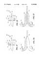
- FIG. 1details means of producing particles, either bichromal as might be used in an electrostatic display, or monochromal as might be used in a dielectrophoretic display, with an implanted dipole moment.
- atomizing nozzles 1are loaded with materials 12 and 13 which may be differently colored.
- a first atomizing nozzlemay be held at a positive potential 3 and a second nozzle may be held at a negative potential 4.
- Such potentialsaid in atomization and impart a charge to droplets which form from said nozzles producing positively charge droplets 5 and negatively charged droplets 6.
- Such opposite charged dropletsare attracted to each other electrostatically forming an overall neutral pair. After the formation of a neutral particle there is no more electrostatic attraction and no additional droplets are attracted to the neutral pair.
- said material 12 and 13is such that the particles are liquid when exiting said nozzles and either cool to form a solid or undergo a chemical reaction which may involve an additional hardening agent to form a solid then said charge may be trapped on each side of said neutral pair forming a bichromal solid particle with an implanted dipole 16.
- suitable choice of materialssuch as polyethylene, polyvinylidene fluoride or other materials such metastable dipoles may persist for long periods of time as is known in the art of electrets.
- a heating element 7may serve to reheat said pair thus minimizing surface tension energy and serving to reform said pair into a more perfect spherical shape.
- a set of electrodes 8 biased at either the same or opposite voltagemay be employed to trap particles which are not overall charge neutral.
- a similar apparatusmay be employed to create a monochromal particle with an implanted dipole.
- nozzles containing material of the same color 12are employed as before to create a monochromal particle with implanted dipole 21.
- FIGS. 1C and 1Dalternative means are shown for producing a bichromal particle with implanted dipole by means of combining two differentially colored materials 12 and 13 on a spinning disk 11 or in a double barreled nozzle 19.
- Said materialsare charged by means of positive electrode 14 and negative electrode 15 and combine by means of electrostatic attraction at the rim of said disk or exit of said double barrel nozzle to form bichromal particle with implanted dipole moment 16.
- Said meansdiffers from that known in the art by means of causing said two different materials 12 and 13 to coalesce by means of electrostatic attraction as opposed to relying on surface properties and interactions between the two materials. Additionally the present scheme creates a particle with an implanted dipole moment 16 which may serve to create a larger dipole moment than that possible from the naturally occurring Zeta potential.
- a similar apparatusmay be employed to create a monochromal particle with an implanted dipole.
- nozzles containing material of the same color 12are employed as before to create a monochromal particle with implanted dipole 21.
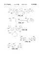
- an internal phase 25which may be a liquid or may be a solid with an additional associated surface layer 27.
- Said internal phaseif liquid or said associated surface layer may contain a polymer building block, such as adipoyl chloride in Silicone Oil.
- Said internal phase, with associated boundary layer in the case of a liquidmay then be dispersed in a continuous phase liquid 30 which may be an aqueous solution which is immiscible with said internal phase or associated surface layer.
- a solution 40which contains another polymer building block or cross linking agent may be added to continuous phase liquid 30.
- Said solution 40has the effect of forming a solid layer at the interface of the internal phase or associated surface layer and said continuous phase liquid 30 thus acting to microencapsulate said internal phase.
- an internal phase 25which may be a solid or a liquid may be caused to pass through a series of liquid films 50,60,70 which may contain polymer building blocks, cross linking agents and overcoat materials such that a final microcapsule 120 results comprised of an internal phase 25, an associated surface layer 27 and an outer shell 80.
- FIG. 2CAn alternate means of microencapsulation is shown in FIG. 2C.
- a light source 82which may be a UV light source passes in some areas through a photomask 84 exposing a crosslinkable polymer which may be caused to form a cellular structure 86.
- the individual cells of said cellular structuremay then be filled with an internal phase 25.
- FIG. 3details such electronically addressable contrast media systems which are suitable for addressing by means of a top clear electrode 100 and bottom electrode 110.
- a microcapsule 120may contain a microsphere with a positively charged hemisphere 142 and a negatively charged 140 hemisphere and an associated surface layer material 130. If said hemispheres are differentially colored an electric field applied to said electrodes may act to change the orientation of said sphere thus causing a perceived change in color.
- a microcapsule 120may contain positively charged particles of one color 210 and negatively charged particles of another color 220 such that application of an electric field to said electrodes causes a migration of the one color or the other color, depending on the polarity of the field, toward the surface of said microcapsule and thus effecting a perceived color change.
- Such a systemconstitutes a microencapsulated electrophoretic system.
- a microcapsule 120may contain a dye, dye precursor or dye indicator material of a given charge polarity 230 or a dye, dye precursor or dye indicator material attached to a particle of given charge polarity such as a microsphere with an appropriate surface group attached and a reducing, oxidizing, proton donating, proton absorbing or solvent agent of the other charge polarity 240 or a reducing, oxidizing, proton donating, proton absorbing or solvent agent attached to a particle of the other charge polarity.
- said dye substance 230is maintained distal to said reducing, oxidizing, proton donating, proton absorbing or solvent agent 240 thus effecting one color state as in FIG. 3C.
- said dye substance and said reducing, oxidizing, proton donating, proton absorbing or solvent agentmay bond to form a complex 245 of second color state.
- Suitable materials for use in this systemare leuco and lactone dye systems and other ring structures which may go from a state of one color to a state of a second color upon application of a reducing, oxidizing or solvent agent or dye indicator systems which may go from a state of one color to a state of a second color upon application of a proton donating or proton absorbing agent as is known in the art.
- An additional gel or polymer materialmay be added to the contents of said microcapsule in order to effect a bistability of the system such that said constituents are relatively immobile except on application of an electric field.
- a microcapsule 120may contain phosphor particle 255 and photoconductive semiconductor particles and dye indicator particles 260 in a suitable binder 250. Applying an AC electric field to electrodes 100 and 110 causes AC electroluminescence which causes free charge to be generated in the semiconducting material further causing said dye indicator to change color state.
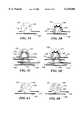
- FIGS. 4A-Mit may be desirable to develop ink systems which are suitable for use without a top transparent electrode 100 which may degrade the optical characteristics of the device.
- the chemistry as described in reference to FIGS. 3C-Dmay be employed with in-plane electrodes such that said chemistry undergoes a color switch from one color state to a second color state upon application of an electric field to in-plane electrodes 270 and 280.
- Such a systemis viewed from above and thus said electrodes may be opaque and do not effect the optical characteristics of said display.
- FIGS. 4C and 4Da bistable liquid crystal system of the type demonstrated by Hatano et. al. of Minolta Corp. is modified to be effected by in plane electrodes such that a liquid crystal mixture transforms from a first transparent planar structure 290 to a second scattering focal conic structure 292.
- the system of FIG. 3Emay be switched by use of in-plane electrodes 270 and 280.
- a hairpin shaped molecule or spring in the closed state 284may have attached to it a positively charged 282 and a negatively charged 283 head which may be microspheres with implanted dipoles. Additionally one side of said hairpin shaped molecule or spring has attached to it a leuco dye 286 and the other side of said hairpin shaped molecule or spring has attached to it a reducing agent 285.
- said leuco dye 286 and said reducing agent 285are brought into proximity such that a bond is formed 287 and said leuco dye is effectively reduced thus effecting a first color state.
- said bond 287may be made to break thus yielding an open state 288.
- said open statethe leuco dye and reducing agent are no longer proximal and the leuco dye, being in a non-reduced state, effects a second color state.
- the systemmay be reversed by applying a DC electric field which serves to reproximate the leuco dye and reducing agent groups.
- Many molecules or microfabricated structuresmay serve as the normally open hairpin shaped molecule or spring. These may include oleic acid like molecules 289. Reducing agents may include sodium dithionite.
- Reducing agentsmay include sodium dithionite.
- the system as discussedis bistable.
- energymay be stored in said hairpin shaped molecule or spring and as such said system may also function as a battery.
- an alternative leucodye-reducing agent systemmay employ a polymer shown in FIG. 4I in a natural state 293.
- a DC electric fieldWhen a DC electric field is applied said polymer assumes a linear shape 294 with leuco 286 and reducing agent 285 groups distal from each other.
- said polymerUpon application of either a reversing DC field or an AC electric field said polymer will tend to coil bringing into random contact said leuco and reducing groups forming a bond 287 with a corresponding color change. Said polymer serves to make said system bistable.
- polymer leuco and reducing groupsmay be attached to oppositely charge microspheres directly by means of a bridge 286 which may be a biotin-streptavidin bridge, polymer bridge or any other suitable bridge.
- a bridge 286may be a biotin-streptavidin bridge, polymer bridge or any other suitable bridge.
- a polymermay be added to aid in the stability of the oxidized state.
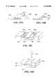
- an entirely different principlemay be employed in an electronically addressable contrast media ink.
- the dielectrophoretic effectis employed in which a species of higher dielectric constant may be caused to move to a region of high electric field strength.
- a non-colored dye solvent complex 315which is stable when no field is applied across electrode pair 150 may be caused to become dissociate into colored dye 300 and solvent 310 components by means of an electric field 170 acting differentially on the dielectric constant of said dye complex and said solvent complex as applied by electrode pair 150.
- the chemistries as discussed in the system of FIGS. 3C-Dmay readily be employed here and that said dye complex and said solvent complex need not themselves have substantially different dielectric constants but rather may be associated with other molecules or particles such as microspheres with substantially different dielectric constants.
- a gel or polymer complexmay be added to the contents of said microcapsule in order to effect a bistability.
- stacked electrode pairs 150 and 160may be employed to effect a high electric field region in a higher 170 or lower 180 plane thus causing a higher dielectric constant material such as one hemisphere of a bichromal microsphere 141 or one species of a mixture of colored species 147 to migrate to a higher or lower plane respectively and give the effect of differing color states.
- materials 165which may be dielectric materials or may be conducting materials may be employed to shape said electric fields.
- FIGS. 6A-Bsystems based on a frequency dependent dielectrophoretic effect are described. Such systems are addressed by means of applying a field of one frequency to produce a given color and applying a field of a different frequency to produce another color. Such a functionality allows for a rear addressed display.
- a microcapsule 120encompasses an internal phase 184 which may be a material which has a frequency independent dielectric constant as shown in Plot 6C, curve 320 and which may have a first color B and material 182 which has a frequency dependent dielectric constant and a second color W. Said frequency dependent material may further have a high dielectric constant at low frequency and a smaller dielectric constant at higher frequency as shown in FIG. 6C 322.
- Application of a low frequency AC field by means of electrodes 270 and 280causes said material 182 to be attracted to the high field region proximal to the electrodes thus causing said microcapsule to appear as the color B when viewed from above.
- a particleis fabricated with an engineered frequency dependent dielectric constant.
- the means for fabricating this particleare depicted in FIGS. 1B, E and F.
- dipolar particlesAt low frequency such dipolar particles have sufficiently small mass that they may rotate in phase with said AC field thus effectively canceling said field and acting as a high dielectric constant material.
- the inertia of said particlesAt high frequency however the inertia of said particles is such that they cannot keep in phase with said AC field and thus fail to cancel said field and consequently have an effectively small dielectric constant.
- material 182may be comprised of naturally occurring frequency dependent dielectric materials.
- material 182may be a natural or artificial cell material which has a dielectric constant frequency dependence as depicted in FIG. 6D, curve 330 as are discussed in Electromechanics of Particles by T. B. Jones incorporated herein by reference. Such particles are further suitable for fabrication of an electronically addressable contrast ink.
- Microcapsule 120contains a particle of a first dielectric constant, conductivity and color 186, a particle of a second dielectric constant, conductivity and color and an internal phase of a third dielectric constant, conductivity and color 190.
- FIG. 6Eit is known in the art of electromechanics of particles that for particles with ohmic loss (e.g. finite conductivity) that at low frequency the DC conductivity governs the dielectric constant whereas at high frequency the dielectric polarization governs the dielectric constant.
- a particle with finite conductivityhas a dielectric constant K as a function of frequency f as in FIG. 6E, curve 338.
- a second particle of second colorhas a dielectric constant K as a function of frequency f as in FIG. 6E, curve 340.
- an internal phase with no conductivityhas a frequency independent dielectric constant K, curve 336.
- FIGS. 7-9depict other types of electronically active ink systems.
- prior art meansare known for depositing metals or resistive materials in a binding medium which may later be cured to form conducting or resistive traces.
- novel meansare described for depositing semiconductive materials in a binder on a large class of substrate materials in one case and for depositing metals, resistive materials or semiconductive materials outside of vacuum, in an arbitrary pattern, without the need for an etch step and on a large class of substrate materials in another case.
- a semiconductor ink 350may be fabricated by dispersing a semiconductor powder 355 in a suitable binder 356.
- Said semiconductive powdermay be Si, Germanium or GaAs or other suitable semiconductor and may further be with n-type impurities such as phosphorus, antimony or arsenic or p-type impurities such as boron, gallium, indium or aluminum or other suitable n or p type dopants as is known in the art of semiconductor fabrication.
- Said binder 356may be a vinyl, plastic heat curable or UV curable material or other suitable binder as is known in the art of conducting inks.
- Said semiconductive ink 350may be applied by printing techniques to form switch or logic structures.
- Said printing techniquesmay include a fluid delivery system 370 in which one or more inks 372, 374 may be printed in a desired pattern on to a substrate.
- said ink system 350may be printed by means of a screen process 377 in which an ink 380 is forced through a patterned aperture mask 378 onto a substrate 379 to form a desired pattern.
- Said ink pattern 360when cured brings into proximity said semiconductive powder particles 355 to create a continuous percolated structure with semiconductive properties 365.
- a systemfor causing a conductive or semiconductive trace 390 to be formed on substrate 388 in correspondence to an impinging light source 382 which may be steered by means of an optical beam steerer 384.
- the operation of said systemis based upon a microcapsule 386 which contains a metal or semiconductive salt in solution.
- light 382which may be a UV light said metal or semiconductive salt is reduced to a metal or semiconductor and said microcapsule is simultaneously burst causing deposition of a conductive or semiconductive trace.
- FIG. 9Aan ink jet system for depositing metallic or semiconductive traces 410 is depicted.
- a jet containing a metal or semiconductive salt 420impinges upon a substrate 400 in conjunction with a jet containing a reducing agent 430.
- a metallic trace silver nitrate (AgNO3)may be used for jet 420 and a suitable aldehyde may be used for the reducing jet 430.
- chemistries suitable for the present systemare known in the art of electroless plating. In all such examples it is understood that said jets are moveable and controllable such that an arbitrary trace may be printed.
- FIG. 9Ba system which is similar to that of FIG. 9A is depicted.
- an electron beam 470may be used instead of said reducing jet in order to bring about a reduction of a metal or semiconductive salt emanating from a jet 460.
- a ground plane 450may be employed to ground said electron beam.
- FIG. 9Can ink jet system for depositing a metallic or semiconductive trace is depicted based on electroplating.
- a metal or semiconductive salt in a jet 480 held at a potential Vmay be electroplated onto a substrate 410 thus forming a metallic or semiconductive trace.
- jet 490may contain a photoconductive material and a metal salt which may be caused to be photoconductively electroplated onto surface 400 by means of application of light source 495 as is known in the field of photoconductive electroplating.
- a systemis depicted for a moveable deposition head 500 which contains a chamber 520 which may be filled with an inert gas via inlet 510 and which further contains thermal, sputtering, electron beam or other deposition means 530.
- Said moveable head 500may print a metal, semiconductor, insulator, spin material or other material in an arbitrary pattern onto a large class of substrates 540. In some case such substrate 540 be cooled or chilled to prevent damage from said materials which may be at an elevated temperature.
- an NPN junction transistormay be fabricated consisting of a n-type emitter 950, a p-type base 954 and a n-type collector 952.
- a field effect transistormay be printed such as a metal oxide semiconductor.
- a transistorconsists of a p-type material 970, an n-type material 966 an n-type inversion layer 968 an oxide layer 962 which acts as the gate a source lead 960 and a drain lead 964.
- a field effect transistormay be printed such as a metal oxide semiconductor.
- Such a transistorconsists of a p-type material 970, an n-type material 966 an n-type inversion layer 968 an oxide layer 962 which acts as the gate a source lead 960 and a drain lead 964.
- multiple layers of logicmay be printed by using an appropriate insulating layer between said logic layers. Further three dimensional interconnects between different logic layers may be accomplished by means of vias in said insulating layers.
- a printed solar cellmay be fabricated by printing some or all of a metal contact layer 972, a p-type layer 974, an n type layer 976 and an insulating layer 978.
- Light 979which impinges upon said structure generates a current as is known in the art of solar cells.
- Such printed solar cellsmay be useful in very thin compact and/or inexpensive structures where power is needed.
- FIGS. 10E-H elements useful for analog circuitrymaybe printed.
- a capacitormay be printed with dielectric material 983 interposing capacitor plates 981 and 985.
- the same structuremay constitute a resistor by replacing dielectric 983 with a resistive material such as carbon ink.
- chokes or radio antennaemay be printed layer by layer.
- a first set of diagonal electrodes 989may be laid down on a substrate.
- an insulator or magnetic core 987On top of this may be printed an insulator or magnetic core 987.
- top electrodes 992 which connect with said bottom electrodesmay be printed this forming an inductor, choke or radio antennae.
- An alternate in plane structureis shown in FIG. 10H in which the flux field 995 is now perpendicular to the structure.
- FIGS. 11-14depict a number of possible such structures which may be fabricated.
- an electronic displaysimilar to one described in a copending patent application, Ser. No. 08/504,896, filed Jul. 20, 1995 by Jacobson, is comprised of electronically addressable contrast media 640, address lines 610 and 620 and logic elements 670 all or some of which may be fabricated with the ink systems and printing means as described in the foregoing descriptions.
- Said Electronic Displaymay additionally comprise a data receiver or transceiver block 672 and a power block 674.
- Said data receiver blockmay further be a wireless radio receiver as pictured in FIG.
- said data receiver or transceiver blockmay be an optelectronic structure, a magnetic inductive coil an electric inductive coupling or an acoustic transducer such as a piezoresistive film.
- Said power block 674may comprise a printed polymer battery as pictured in FIG. 11C which consists of in one instance a lithium film 686, a propylene carbonate LiPF 6 film 688 and aLiCoO 2 in matrix 690.
- Said power blockmay alternatively consist of any other battery structure as known in the art of thin structure batteries, a magnetic or electric inductive converter for means of power reception as known in the art, a solar cell which may be a printed solar cell or a semiconductive electrochemical cell which may further have an integral fuel cell for energy storage or a piezoelectric material which generates power when flexed.
- Such a display 600 as described above further comprising a data receiver or transceiver 672 and power block 674 in which some or all of said components are printedmay comprise an inexpensive, lightweight, flexible receiver for visual data and text which we may term "radio paper.”
- datamight be transmitted to the "radio paper” sheet and there displayed thus forming a completely novel type of newspaper, namely one which is continuously updated.
- an electrostatic motorwhich may form an analog clock or watch is depicted which consists of printed conducting elements 720, 730, 740 and 760 which are printed onto substrate 700. Said elements, when caused to alternately switch between positive negative or neutral states by means of a logic control circuit 710 may cause an element 750 to be translated thus forming a motor or actuator.
- a logic control circuit 710may cause an element 750 to be translated thus forming a motor or actuator.
- some or all of said conducting elements and/or logic control elementsmay be printed using the ink systems and printing means described in the foregoing description.
- a wrist watch 800is depicted in which the band 820 of said watch contains an electronically addressable display 830 in which some or all of the components of said display, including the electronically addressable contrast media, the address lines and/or the logic are fabricated by means of the ink systems and printing means described in the foregoing description. Such a fabrication may be useful in terms of producing an inexpensive, easily manufacturable and thin display function. Control buttons 810 may serve to control aspects of said display 830.
- FIG. 13Bit is presently a problem to transmit data or power to a watch band via a wire connection as such connections tend to become spoiled by means of motion of the watchband relative to the watch.
- FIG. 13Bdescribes a system in which a magnetic or electric inductor 832 in watch band 820 may receive or transmit power or data to a magnetic or electric inductor 834 in watch 800 thus eliminating said wired connection.
- Said inductor 832 and 834may be printed structures.
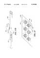
- a spin computeris depicted in which dipoles 912 with dipole moment 914 are situated at the nodes of row 920 and column 930 address lines.
- Such a computerworks by means of initially addressing said dipoles to an initial condition by said address lines and then allowing dipole interactions to produce a final state of the system as a whole thus performing a calculation as is known in the art of Spin Ising models and cellular automata.
- Said dipolesmay consist of a dipolar microsphere 912 microencapsulated in a microcapsule 910 or may consist of another form of dipole and/or another means of encapsulation.
Landscapes
- Engineering & Computer Science (AREA)
- Physics & Mathematics (AREA)
- Chemical & Material Sciences (AREA)
- General Physics & Mathematics (AREA)
- Theoretical Computer Science (AREA)
- Life Sciences & Earth Sciences (AREA)
- Optics & Photonics (AREA)
- Wood Science & Technology (AREA)
- Human Computer Interaction (AREA)
- Nonlinear Science (AREA)
- General Engineering & Computer Science (AREA)
- Organic Chemistry (AREA)
- Crystallography & Structural Chemistry (AREA)
- Nanotechnology (AREA)
- Materials Engineering (AREA)
- Mathematical Physics (AREA)
- Biophysics (AREA)
- Health & Medical Sciences (AREA)
- Molecular Biology (AREA)
- Dispersion Chemistry (AREA)
- Multimedia (AREA)
- Electrochromic Elements, Electrophoresis, Or Variable Reflection Or Absorption Elements (AREA)
Abstract
Description
This application claims priority to U.S. Provisional Application No. 60/035,622, filed Sep. 24, 1996 and claims priority to and is a continuation-in-part of International application PCT/US96/13469, filed Aug. 20, 1996 which claims priority to U.S. Provisional Application No. 60/022,222, filed Jul. 19, 1996 the contents of which are incorporated herein by reference in their entirety.
Currently, printing of conductors and resistors is well known in the art of circuit board manufacture. In order to incorporate logic elements the standard practice is to surface mount semiconductor chips onto said circuit board. To date there does not exist a system for directly printing said logic elements onto an arbitrary substrate.
In the area of flat panel display drivers there exists technology for laying down logic elements onto glass by means of vacuum depositing silicon or other semiconductive material and subsequently etching circuits and logic elements. Such a technology is not amenable to laying down logic elements onto an arbitrary surface due to the presence of the vacuum requirement and the etch step.
In the area of electronically addressable contrast media (as may be used to effect a flat panel display) emissive and reflective electronically active films (such as electroluminscent and electrochromic films), polymer dispersed liquid crystal films, and bichromal microsphere elastomeric slabs are known. No such directly electronically addressable contrast medium however is amenable to printing onto an arbitrary surface.
Finally in the area of surface actuators electrostatic motors, which may be etched or non-etched, are known in the art. In the first case, such etched devices suffer from their inability to be fabricated on arbitrary surfaces. In the second case, non-etched devices suffer from the inability to incorporate drive logic and electronic control directly onto the actuating surface.
It is an object of the present disclosure to overcome the limitations of the prior art in the area of printable logic, display and actuation.
In general the present invention provides a system of electronically active inks and means for printing said inks in an arbitrary pattern onto a large class of substrates without the requirements of standard vacuum processing or etching. Said inks may incorporate mechanical, electrical or other properties and may provide but are not limited to the following function: conducting, insulating, resistive, magnetic, semiconductive, light modulating, piezoelectric, spin, optoelectronic, thermoelectric or radio frequency.
In one embodiment this invention provides for a microencapsulated electric field actuated contrast ink system suitable for addressing by means of top and bottom electrodes or solely bottom electrodes and which operates by means of a bichromal dipolar microsphere, electrophoretic, dye system, liquid crystal, electroluminescent dye system or dielectrophoretic effect. Such an ink system may be useful in fabricating an electronically addressable display on any of a large class of substrate materials which may be thin, flexible and may result in an inexpensive display.
In another embodiment this invention provides for a semiconductive ink system in which a semiconductor material is deployed in a binder such that when said binder is cured a percolated structure with semiconductive properties results.
In another embodiment this invention for provides for systems capable of printing an arbitrary pattern of metal or semiconductive materials by means of photoreduction of a salt, electron beam reduction of a salt, jet electroplating, dual jet electroless plating or inert gas or local vacuum thermal, sputtering or electron beam deposition.
In another embodiment this invention provides for semiconductor logic elements and electro-optical elements which may include diode, transistor, light emitting, light sensing or solar cell elements which are fabricated by means of a printing process or which employ an electronically active ink system as described in the aforementioned embodiments. Additionally said elements may be multilayered and may form multilayer logic including vias and three dimensional interconnects.
In another embodiment this invention provides for analog circuits elements which may include resistors, capacitors, inductors or elements which may be used in radio applications or magnetic or electric field transmission of power or data.
In another embodiment this invention provides for an electronically addressable display in which some or all of address lines, electronically addressable contrast media, logic or power are fabricated by means of a printing process or which employ an electronically active ink system as described in the aforementioned embodiments. Such display may further comprise a radio receiver or transceiver and power means thus forming a display sheet capable of receiving wireless data and displaying the same.
In another embodiment this invention provides for an electrostatic actuator or motor which may be in the form of a clock or watch in which some or all of address lines, logic or power are fabricated by means of a printing process or which employ an electronically active ink system as described in the aforementioned embodiments.
In another embodiment this invention provides for a wrist watch band which includes an electronically addressable display in which some or all of address lines, electronically addressable contrast media, logic or power are fabricated by means of a printing process or which employ an electronically active ink system as described in the aforementioned embodiments. Said watch band may be formed such that it has no external connections but rather receives data and or power by means of electric or magnetic field flux coupling by means of an antennae which may be a printed antennae.
In another embodiment this invention provides for a spin computer in which some or all of address lines, electronically addressable spin media, logic or power are fabricated by means of a printing process or which employ an electronically active ink system as described in the aforementioned embodiments.
Further features and aspects will become apparent from the following description and from the claims.
The foregoing and other objects, features and advantages of the invention will be apparent from the following more particular description of preferred embodiments of the invention, as illustrated in the accompanying drawings in which like reference characters refer to the same parts throughout the different views. The drawings are not necessarily to scale, emphasis instead being placed upon illustrating the principles of the invention.
FIGS. 1A, 1B, 1C, 1D, 1E, and 1F are schematic representations of means of fabricating particles with a permanent dipole moment.
FIGS. 2A, 2B and 2C are schematic representations of means of microencapsulation.
FIGS. 3A, 3B, 3C, 3D, and 3E are schematic representations of microencapsulated electronically addressable contrast media systems suitable for top to bottom addressing.
FIGS. 4A, 4B, 4C, 4D, 4E, 4F, 4G, 4H, 4I, 4J, 4K, 4L, and 4M are schematic representations of microencapsulated electronically addressable contrast media systems suitable for bottom addressing.
FIGS. 5A, 5B, 5C, and 5D are schematic representations of microencapsulated electronically addressable contrast media systems based on a dielectrophoretic effect.
FIGS. 6A and 6B are schematic representations of microencapsulated electronically addressable contrast media systems based on a frequency dependent dielectrophoretic effect.
FIGS. 6C, 6D, and 6E are plots of the dielectric parameter as a function of frequency for various physical systems.
FIGS. 7A, 7B, 7C, and 7D are schematic representations of electronic ink systems and means for printing the same.
FIG. 8 is a schematic representation of a laser reduced metal salt ink system.
FIGS. 9A, 9B, 9C, 9D, and 9E are schematic representations of electronic ink systems and means for printing the same.
FIGS. 10A, 10B, and 10C are schematic diagrams of printed transistor structures.
FIG. 10D is a schematic diagram of a printed optoelectronic element.
FIGS. 10E, 10F, 10G, and 10H are schematic diagrams of printed analog circuit elements.
FIGS. 11A, 11B, and 11C are a schematic diagram of an electronic display employing printed elements; this display may further include a data receiver or transceiver and a power means.
FIG. 12 is a schematic diagram of an electrostatic motor which may be in the form of a watch or clock in which said electrostatic elements are printed
FIGS. 13A and 13B are a schematic diagram of a watch in which the wristband of said watch incorporates an electronically addressable display having printed elements and which may further comprise wireless means for sending or receiving data or power between watch and watchband.
FIG. 14 is a schematic diagram of a spin computer.
Means are known in the prior art for producing bichromal particles or microspheres for use in electronic displays. Such techniques produce a particle that does not have an implanted dipole moment but rather relies in general on the Zeta potential of the material to create a permanent dipole. Such a scheme suffers from the fact that it links the material properties to the electronic properties thus limiting the size of the dipole moment which may be created. FIG. 1 details means of producing particles, either bichromal as might be used in an electrostatic display, or monochromal as might be used in a dielectrophoretic display, with an implanted dipole moment.
Referring to FIG.1A atomizing nozzles 1 are loaded withmaterials positive potential 3 and a second nozzle may be held at anegative potential 4. Such potentials aid in atomization and impart a charge to droplets which form from said nozzles producing positively charge droplets 5 and negatively charged droplets 6. Such opposite charged droplets are attracted to each other electrostatically forming an overall neutral pair. After the formation of a neutral particle there is no more electrostatic attraction and no additional droplets are attracted to the neutral pair. If saidmaterial dipole 16. By suitable choice of materials such as polyethylene, polyvinylidene fluoride or other materials such metastable dipoles may persist for long periods of time as is known in the art of electrets. A heating element 7 may serve to reheat said pair thus minimizing surface tension energy and serving to reform said pair into a more perfect spherical shape. Finally a set ofelectrodes 8 biased at either the same or opposite voltage may be employed to trap particles which are not overall charge neutral.
Referring to FIG. 1B a similar apparatus may be employed to create a monochromal particle with an implanted dipole. In this arrangement nozzles containing material of thesame color 12 are employed as before to create a monochromal particle with implanteddipole 21.
Referring to FIGS. 1C and 1D alternative means are shown for producing a bichromal particle with implanted dipole by means of combining two differentiallycolored materials spinning disk 11 or in a double barrelednozzle 19. Said materials are charged by means ofpositive electrode 14 andnegative electrode 15 and combine by means of electrostatic attraction at the rim of said disk or exit of said double barrel nozzle to form bichromal particle with implanteddipole moment 16. Said means differs from that known in the art by means of causing said twodifferent materials dipole moment 16 which may serve to create a larger dipole moment than that possible from the naturally occurring Zeta potential.
Referring to FIGS. 1E and 1F a similar apparatus may be employed to create a monochromal particle with an implanted dipole. In this arrangement nozzles containing material of thesame color 12 are employed as before to create a monochromal particle with implanteddipole 21.
A large number of techniques are known in the literature for microencapsulating one material inside another material. Such techniques are generally used in the paper or pharmaceutical industry and do not generally produce a microcapsule which embodies simultaneously the properties of optical clarity, high dielectric strength, impermeability and resistance to pressure. With proper modification however these techniques may be made amenable to microencapsulating systems with electronic properties.
Referring to FIG. 2A aninternal phase 25 which may be a liquid or may be a solid with an additional associatedsurface layer 27. Said internal phase if liquid or said associated surface layer may contain a polymer building block, such as adipoyl chloride in Silicone Oil. Said internal phase, with associated boundary layer in the case of a liquid, may then be dispersed in acontinuous phase liquid 30 which may be an aqueous solution which is immiscible with said internal phase or associated surface layer. Finally asolution 40 which contains another polymer building block or cross linking agent may be added tocontinuous phase liquid 30. Saidsolution 40 has the effect of forming a solid layer at the interface of the internal phase or associated surface layer and said continuous phase liquid 30 thus acting to microencapsulate said internal phase.
Referring to FIG. 2B aninternal phase 25 which may be a solid or a liquid may be caused to pass through a series ofliquid films final microcapsule 120 results comprised of aninternal phase 25, an associatedsurface layer 27 and anouter shell 80.
An alternate means of microencapsulation is shown in FIG. 2C. In this scheme alight source 82 which may be a UV light source passes in some areas through aphotomask 84 exposing a crosslinkable polymer which may be caused to form acellular structure 86. The individual cells of said cellular structure may then be filled with aninternal phase 25.
Employing the systems described in FIGS. 2A-C it is possible to microencapsulate systems with electronically active properties specifically electronically addressable contrast media. FIG. 3 details such electronically addressable contrast media systems which are suitable for addressing by means of a topclear electrode 100 andbottom electrode 110. Referring to FIG. 3A amicrocapsule 120 may contain a microsphere with a positively chargedhemisphere 142 and a negatively charged 140 hemisphere and an associatedsurface layer material 130. If said hemispheres are differentially colored an electric field applied to said electrodes may act to change the orientation of said sphere thus causing a perceived change in color.
Referring to FIG. 3B amicrocapsule 120 may contain positively charged particles of onecolor 210 and negatively charged particles of anothercolor 220 such that application of an electric field to said electrodes causes a migration of the one color or the other color, depending on the polarity of the field, toward the surface of said microcapsule and thus effecting a perceived color change. Such a system constitutes a microencapsulated electrophoretic system.
Referring to FIGS. 3C-D amicrocapsule 120 may contain a dye, dye precursor or dye indicator material of a givencharge polarity 230 or a dye, dye precursor or dye indicator material attached to a particle of given charge polarity such as a microsphere with an appropriate surface group attached and a reducing, oxidizing, proton donating, proton absorbing or solvent agent of theother charge polarity 240 or a reducing, oxidizing, proton donating, proton absorbing or solvent agent attached to a particle of the other charge polarity. Under application of an electric field saiddye substance 230 is maintained distal to said reducing, oxidizing, proton donating, proton absorbing orsolvent agent 240 thus effecting one color state as in FIG. 3C. Upon de-application of said electric field said dye substance and said reducing, oxidizing, proton donating, proton absorbing or solvent agent may bond to form a complex 245 of second color state. Suitable materials for use in this system are leuco and lactone dye systems and other ring structures which may go from a state of one color to a state of a second color upon application of a reducing, oxidizing or solvent agent or dye indicator systems which may go from a state of one color to a state of a second color upon application of a proton donating or proton absorbing agent as is known in the art. An additional gel or polymer material may be added to the contents of said microcapsule in order to effect a bistability of the system such that said constituents are relatively immobile except on application of an electric field.
Referring to FIG. 3E amicrocapsule 120 may containphosphor particle 255 and photoconductive semiconductor particles anddye indicator particles 260 in asuitable binder 250. Applying an AC electric field toelectrodes
Referring to FIGS. 4A-M it may be desirable to develop ink systems which are suitable for use without a toptransparent electrode 100 which may degrade the optical characteristics of the device. Referring to FIGS. 4A and B the chemistry as described in reference to FIGS. 3C-D may be employed with in-plane electrodes such that said chemistry undergoes a color switch from one color state to a second color state upon application of an electric field to in-plane electrodes
As another system in-plane switching techniques have been employed in transmissive LCD displays for another purpose, namely to increase viewing angle of such displays. Referring to FIGS. 4C and 4D a bistable liquid crystal system of the type demonstrated by Hatano et. al. of Minolta Corp. is modified to be effected by in plane electrodes such that a liquid crystal mixture transforms from a first transparentplanar structure 290 to a second scattering focalconic structure 292.
Referring to FIG. 4E the system of FIG. 3E may be switched by use of in-plane electrodes
Other systems may be created which cause a first color change by means of applying an AC field and a second color change by means of application of either a DC field or an AC field of another frequency. Referring to FIGS. 4F-G a hairpin shaped molecule or spring in theclosed state 284 may have attached to it a positively charged 282 and a negatively charged 283 head which may be microspheres with implanted dipoles. Additionally one side of said hairpin shaped molecule or spring has attached to it aleuco dye 286 and the other side of said hairpin shaped molecule or spring has attached to it a reducingagent 285. When said molecule or spring is in theclosed state 284 then saidleuco dye 286 and said reducingagent 285 are brought into proximity such that a bond is formed 287 and said leuco dye is effectively reduced thus effecting a first color state. Upon a applying an AC electric field with frequency that is resonant with the vibrational mode of said charged heads cantilevered on said hairpin shaped molecule or spring saidbond 287 may be made to break thus yielding anopen state 288. In said open state the leuco dye and reducing agent are no longer proximal and the leuco dye, being in a non-reduced state, effects a second color state. The system may be reversed by applying a DC electric field which serves to reproximate the leuco dye and reducing agent groups. Many molecules or microfabricated structures may serve as the normally open hairpin shaped molecule or spring. These may include oleic acid likemolecules 289. Reducing agents may include sodium dithionite. We note that the system as discussed is bistable. We note also that energy may be stored in said hairpin shaped molecule or spring and as such said system may also function as a battery.
Referring to FIGS. 4I-K an alternative leucodye-reducing agent system may employ a polymer shown in FIG. 4I in anatural state 293. When a DC electric field is applied said polymer assumes alinear shape 294 withleuco 286 and reducingagent 285 groups distal from each other. Upon application of either a reversing DC field or an AC electric field said polymer will tend to coil bringing into random contact said leuco and reducing groups forming abond 287 with a corresponding color change. Said polymer serves to make said system bistable.
Referring to FIGS. 4L and 4M a similar system is possible but instead polymer leuco and reducing groups may be attached to oppositely charge microspheres directly by means of abridge 286 which may be a biotin-streptavidin bridge, polymer bridge or any other suitable bridge. As before application of a DC field cause leuco and reducing groups to become distal whereas application of a reverse DC field or AC field brings into random contact the leuco and reducing groups. A polymer may be added to aid in the stability of the oxidized state.
Referring to FIGS. 5A-D and FIGS. 6A-B an entirely different principle may be employed in an electronically addressable contrast media ink. In these systems the dielectrophoretic effect is employed in which a species of higher dielectric constant may be caused to move to a region of high electric field strength.
Referring to FIGS. 5A and 5B a non-colored dye solvent complex 315 which is stable when no field is applied acrosselectrode pair 150 may be caused to become dissociate intocolored dye 300 and solvent 310 components by means of anelectric field 170 acting differentially on the dielectric constant of said dye complex and said solvent complex as applied byelectrode pair 150. It is understood that the chemistries as discussed in the system of FIGS. 3C-D may readily be employed here and that said dye complex and said solvent complex need not themselves have substantially different dielectric constants but rather may be associated with other molecules or particles such as microspheres with substantially different dielectric constants. Finally it is understood that a gel or polymer complex may be added to the contents of said microcapsule in order to effect a bistability.
Referring to FIGS. 5C-D stacked electrode pairs 150 and 160 may be employed to effect a high electric field region in a higher 170 or lower 180 plane thus causing a higher dielectric constant material such as one hemisphere of abichromal microsphere 141 or one species of a mixture of coloredspecies 147 to migrate to a higher or lower plane respectively and give the effect of differing color states. Insuch schemes materials 165 which may be dielectric materials or may be conducting materials may be employed to shape said electric fields.
Referring to FIGS. 6A-B, systems based on a frequency dependent dielectrophoretic effect are described. Such systems are addressed by means of applying a field of one frequency to produce a given color and applying a field of a different frequency to produce another color. Such a functionality allows for a rear addressed display.
Referring to FIG. 6A, amicrocapsule 120 encompasses aninternal phase 184 which may be a material which has a frequency independent dielectric constant as shown in Plot 6C,curve 320 and which may have a first color B andmaterial 182 which has a frequency dependent dielectric constant and a second color W. Said frequency dependent material may further have a high dielectric constant at low frequency and a smaller dielectric constant at higher frequency as shown in FIG.6C 322. Application of a low frequency AC field by means ofelectrodes material 182 to be attracted to the high field region proximal to the electrodes thus causing said microcapsule to appear as the color B when viewed from above. Conversely application of a high frequency AC field by means ofelectrodes material 184 to be attracted to the high field region proximal the electrodes thus displacingmaterial 182 and thus causing said microcapsule to appear as the color W when viewed from above. If B and W correspond to Black and White then a black and white display may be effected. A polymer material may be added tointernal phase 184 to cause said system to be bistable in the field off condition. Alternatively stiction to the internal side wall of said capsule may cause bistability.
Referring to FIG. 6A,material 182 and FIG. 6C, a particle is fabricated with an engineered frequency dependent dielectric constant. The means for fabricating this particle are depicted in FIGS. 1B, E and F. At low frequency such dipolar particles have sufficiently small mass that they may rotate in phase with said AC field thus effectively canceling said field and acting as a high dielectric constant material. At high frequency however the inertia of said particles is such that they cannot keep in phase with said AC field and thus fail to cancel said field and consequently have an effectively small dielectric constant.
Alternatively material 182 may be comprised of naturally occurring frequency dependent dielectric materials. Materials which obey a frequency dependence functionality similar to the artificially created dipole material discussed above and which follow curves similar to FIG. 6C,curve 322 include materials such as Hevea rubber compound which has a dielectric constant of K=36 at f=103 Hz and K=9 at f=106 Hz, materials with ohmic loss as are known in Electromechanics of Particles by T. B. Jones incorporated herein by reference and macromolecules with permanent dipole moments.
Additionally material 182 may be a natural or artificial cell material which has a dielectric constant frequency dependence as depicted in FIG. 6D,curve 330 as are discussed in Electromechanics of Particles by T. B. Jones incorporated herein by reference. Such particles are further suitable for fabrication of an electronically addressable contrast ink.
Referring to FIG. 6B a system is depicted capable of effecting a color display.Microcapsule 120 contains a particle of a first dielectric constant, conductivity andcolor 186, a particle of a second dielectric constant, conductivity and color and an internal phase of a third dielectric constant, conductivity andcolor 190. Referring to FIG. 6E it is known in the art of electromechanics of particles that for particles with ohmic loss (e.g. finite conductivity) that at low frequency the DC conductivity governs the dielectric constant whereas at high frequency the dielectric polarization governs the dielectric constant. Thus a particle with finite conductivity has a dielectric constant K as a function of frequency f as in FIG. 6E,curve 338. A second particle of second color has a dielectric constant K as a function of frequency f as in FIG. 6E,curve 340. Finally an internal phase with no conductivity has a frequency independent dielectric constant K,curve 336. If an AC field of frequency f1 is applied by means ofelectrodes material 186 of color M will be attracted to the high field region proximal to said electrodes thus causing said microcapsule to appear as a mixture of the colors C and Y, due to the other particle and internal phase respectively, when viewed from above. If an AC field of frequency f2 is applied by means ofelectrodes material 188 of color Y will be attracted to the high field region proximal to said electrodes thus causing said microcapsule to appear as a mixture of the colors C and M when viewed from above. Finally if an AC field of frequency f3 is applied by means ofelectrodes internal phase 190 of color C will be attracted to the high field region proximal to said electrodes thus causing said microcapsule to appear as a mixture of the colors M and Y when viewed from above. If C, M and Y correspond to Cyan, Magenta and Yellow a color display may be effected.
It is understood that many other combinations of particles with frequency dependent dielectric constants arising from the physical processes discussed above may be employed to effect a frequency dependent electronically addressable display.
In addition to the microencapsulated electronically addressable contrast media ink discussed in FIGS. 3-6, FIGS. 7-9 depict other types of electronically active ink systems. In the prior art means are known for depositing metals or resistive materials in a binding medium which may later be cured to form conducting or resistive traces. In the following description novel means are described for depositing semiconductive materials in a binder on a large class of substrate materials in one case and for depositing metals, resistive materials or semiconductive materials outside of vacuum, in an arbitrary pattern, without the need for an etch step and on a large class of substrate materials in another case.
In one system asemiconductor ink 350 may be fabricated by dispersing asemiconductor powder 355 in asuitable binder 356. Said semiconductive powder may be Si, Germanium or GaAs or other suitable semiconductor and may further be with n-type impurities such as phosphorus, antimony or arsenic or p-type impurities such as boron, gallium, indium or aluminum or other suitable n or p type dopants as is known in the art of semiconductor fabrication.Said binder 356 may be a vinyl, plastic heat curable or UV curable material or other suitable binder as is known in the art of conducting inks. Saidsemiconductive ink 350 may be applied by printing techniques to form switch or logic structures. Said printing techniques may include afluid delivery system 370 in which one ormore inks ink system 350 may be printed by means of ascreen process 377 in which anink 380 is forced through a patternedaperture mask 378 onto asubstrate 379 to form a desired pattern. Saidink pattern 360 when cured brings into proximity saidsemiconductive powder particles 355 to create a continuous percolated structure withsemiconductive properties 365.
Referring to FIG. 8 a system is depicted for causing a conductive orsemiconductive trace 390 to be formed onsubstrate 388 in correspondence to an impinginglight source 382 which may be steered by means of anoptical beam steerer 384. The operation of said system is based upon amicrocapsule 386 which contains a metal or semiconductive salt in solution. Upon being exposed to light 382 which may be a UV light said metal or semiconductive salt is reduced to a metal or semiconductor and said microcapsule is simultaneously burst causing deposition of a conductive or semiconductive trace.
Referring to FIG. 9A an ink jet system for depositing metallic or semiconductive traces 410 is depicted. In this system a jet containing a metal orsemiconductive salt 420 impinges upon asubstrate 400 in conjunction with a jet containing a reducingagent 430. As an example, to form a metallic trace silver nitrate (AgNO3) may be used forjet 420 and a suitable aldehyde may be used for the reducingjet 430. Many other examples of chemistries suitable for the present system are known in the art of electroless plating. In all such examples it is understood that said jets are moveable and controllable such that an arbitrary trace may be printed.
Referring to FIG. 9B a system which is similar to that of FIG. 9A is depicted. In this case anelectron beam 470 may be used instead of said reducing jet in order to bring about a reduction of a metal or semiconductive salt emanating from ajet 460. Aground plane 450 may be employed to ground said electron beam.
Referring to FIG. 9C an ink jet system for depositing a metallic or semiconductive trace is depicted based on electroplating. In this system a metal or semiconductive salt in ajet 480 held at a potential V may be electroplated onto asubstrate 410 thus forming a metallic or semiconductive trace.
Referring to FIG. 9D means are known in the prior art for UV reduction of a metal salt from an ink jet head. In the present system a jet containing a metal orsemiconductive salt 490 may be incident upon asubstrate 400 in conjunction with a directedlight beam 495 such that said metal or semiconductive salt is reduced into a conductive orsemiconductive trace 410. Alternativelyjet 490 may contain a photoconductive material and a metal salt which may be caused to be photoconductively electroplated ontosurface 400 by means of application oflight source 495 as is known in the field of photoconductive electroplating.
Referring to FIG. 9E a system is depicted for amoveable deposition head 500 which contains achamber 520 which may be filled with an inert gas viainlet 510 and which further contains thermal, sputtering, electron beam or other deposition means 530. Saidmoveable head 500 may print a metal, semiconductor, insulator, spin material or other material in an arbitrary pattern onto a large class ofsubstrates 540. In some casesuch substrate 540 be cooled or chilled to prevent damage from said materials which may be at an elevated temperature.
Referring to FIG. 10 said previously described electronically active ink systems and printing means may be applied to form switch or logic structures, optoelectronic structures or structures useful in radio or magnetic or electric field transmission of signals or power. As indicated in FIGS. 10A-B an NPN junction transistor may be fabricated consisting of a n-type emitter 950, a p-type base 954 and a n-type collector 952.
Alternatively a field effect transistor may be printed such as a metal oxide semiconductor. Such a transistor consists of a p-type material 970, an n-type material 966 an n-type inversion layer 968 anoxide layer 962 which acts as the gate asource lead 960 and adrain lead 964. It is readily understood that multiple layers of logic may be printed by using an appropriate insulating layer between said logic layers. Further three dimensional interconnects between different logic layers may be accomplished by means of vias in said insulating layers.
Referring to FIG. 10D a printed solar cell may be fabricated by printing some or all of ametal contact layer 972, a p-type layer 974, ann type layer 976 and an insulatinglayer 978.Light 979 which impinges upon said structure generates a current as is known in the art of solar cells. Such printed solar cells may be useful in very thin compact and/or inexpensive structures where power is needed.
Referring to FIGS. 10E-H elements useful for analog circuitry maybe printed. Referring to FIG. 10E a capacitor may be printed withdielectric material 983 interposingcapacitor plates
Referring to FIGS. 10F-H inductors, chokes or radio antennae may be printed layer by layer. Referring to FIGS. 10F and G a first set ofdiagonal electrodes 989 may be laid down on a substrate. On top of this may be printed an insulator ormagnetic core 987. Finallytop electrodes 992 which connect with said bottom electrodes may be printed this forming an inductor, choke or radio antennae. An alternate in plane structure is shown in FIG. 10H in which theflux field 995 is now perpendicular to the structure.
The ink systems and printing means discussed in the foregoing descriptions may be useful for the fabrication of a large class of electronically functional structures. FIGS. 11-14 depict a number of possible such structures which may be fabricated.
Referring to FIG. 11A, an electronic display, similar to one described in a copending patent application, Ser. No. 08/504,896, filed Jul. 20, 1995 by Jacobson, is comprised of electronicallyaddressable contrast media 640,address lines logic elements 670 all or some of which may be fabricated with the ink systems and printing means as described in the foregoing descriptions. Said Electronic Display may additionally comprise a data receiver ortransceiver block 672 and apower block 674. Said data receiver block may further be a wireless radio receiver as pictured in FIG. 11B in which some or all of the components thereof includingantennae 676, inductor or choke 678, diode, 680,capacitor 682,NPN transistor 684,resistor 681, conductingconnection 677 orinsulation overpass 675 may be printed by the means discussed above. Alternatively said data receiver or transceiver block may be an optelectronic structure, a magnetic inductive coil an electric inductive coupling or an acoustic transducer such as a piezoresistive film.
Saidpower block 674 may comprise a printed polymer battery as pictured in FIG. 11C which consists of in one instance alithium film 686, a propylene carbonate LiPF6 film 688 and aLiCoO2 inmatrix 690. Said power block may alternatively consist of any other battery structure as known in the art of thin structure batteries, a magnetic or electric inductive converter for means of power reception as known in the art, a solar cell which may be a printed solar cell or a semiconductive electrochemical cell which may further have an integral fuel cell for energy storage or a piezoelectric material which generates power when flexed.
Such adisplay 600 as described above further comprising a data receiver ortransceiver 672 andpower block 674 in which some or all of said components are printed may comprise an inexpensive, lightweight, flexible receiver for visual data and text which we may term "radio paper." In such a system data might be transmitted to the "radio paper" sheet and there displayed thus forming a completely novel type of newspaper, namely one which is continuously updated.
Referring to FIG. 12 an electrostatic motor which may form an analog clock or watch is depicted which consists of printed conductingelements substrate 700. Said elements, when caused to alternately switch between positive negative or neutral states by means of alogic control circuit 710 may cause anelement 750 to be translated thus forming a motor or actuator. In the device of FIG. 12 some or all of said conducting elements and/or logic control elements may be printed using the ink systems and printing means described in the foregoing description.
Referring to FIG. 13A awrist watch 800 is depicted in which theband 820 of said watch contains an electronicallyaddressable display 830 in which some or all of the components of said display, including the electronically addressable contrast media, the address lines and/or the logic are fabricated by means of the ink systems and printing means described in the foregoing description. Such a fabrication may be useful in terms of producing an inexpensive, easily manufacturable and thin display function.Control buttons 810 may serve to control aspects of saiddisplay 830.
Referring to FIG. 13B it is presently a problem to transmit data or power to a watch band via a wire connection as such connections tend to become spoiled by means of motion of the watchband relative to the watch. In order to overcome this FIG. 13B describes a system in which a magnetic orelectric inductor 832 inwatch band 820 may receive or transmit power or data to a magnetic orelectric inductor 834 inwatch 800 thus eliminating said wired connection. Saidinductor
Referring to FIG. 14, a spin computer is depicted in whichdipoles 912 withdipole moment 914 are situated at the nodes ofrow 920 andcolumn 930 address lines. Such a computer works by means of initially addressing said dipoles to an initial condition by said address lines and then allowing dipole interactions to produce a final state of the system as a whole thus performing a calculation as is known in the art of Spin Ising models and cellular automata. Said dipoles may consist of adipolar microsphere 912 microencapsulated in amicrocapsule 910 or may consist of another form of dipole and/or another means of encapsulation.
While this invention has been particularly shown and described with references to preferred embodiments thereof, it will be understood by those skilled in the art that various changes in form and details may be made therein without departing from the spirit and scope of the invention as defined by the appended claims.
Claims (18)
1. An electrically addressable ink comprising a microcapsule, said microcapsule comprising:
a first particle having a first charge; and
a second particle having a second charge;
wherein applying an electric field having a first polarity to said microcapsule effects a perceived optical property change by causing one of said first and second particles to migrate in a direction responsive to said field.
2. The ink of claim 1 wherein both said first and said second particles move in response to said electric field.
3. The ink of claim 1 wherein said first particle has a color.
4. The ink of claim 1 wherein said first particle comprises a dye.
5. The ink of claim 1 wherein the first particle further comprises a dye indicator system.
6. The ink of claim 1 wherein said microcapsule further comprises a material such that said first and second particles are substantially immobile in the absence of an electric field.
7. The ink of claim 1 wherein said second particle comprises a substance capable of reacting with said first particle, whereupon the application of a first electric field causes said first particle to be maintained separate from said substance such that said ink is maintained in a first color state; and whereupon application of a second electric field said first particle and said substance react to form a compound having a second color state.
8. The ink of claim 7 wherein said first particle and said substance react to form a compound having a color state when at least one of said first and second electric fields is zero.
9. The ink of claim 1 wherein said first particle comprises a ring structure coupled to a first head having a first charge, and said second particle comprises a substance coupled to a second head having a second charge;
wherein application of an electric field causes said ring structure and said substance to become separated from each other, effecting a first color state.
10. The ink of claim 9 wherein application of a second electric field brings said ring structure and said substance into contact to effect a second color state.
11. A microencapsulated ink system, comprising:
a microcapsule comprising:
a photoconductive semiconductor particle; and
a dye indicator particle;
wherein the application of an electric field to said microcapsule causes said photoconductive semiconductor particle to generate free charge, causing the dye indicator to effect a first color state.
12. An electrically addressable ink comprising a microcapsule, said microcapsule comprising:
a hairpin-shaped molecule having a first portion and a second portion, said hair-pin shaped molecule comprising:
a first moiety having a first charge attached to said first portion of said hairpin-shaped molecule; and
a second moiety having a second charge attached to said second portion of said hairpin-shaped molecule, said second moiety capable of reacting with said first moiety, said second charge being opposite to said first charge;
the reaction between said first moiety and said second moiety defining a closed state of said hairpin-shaped molecule effecting a first color state; and
the separation of said first moiety from said second moiety defining an open state of said hairpin-shaped molecule, effecting a second color state.
13. The ink of claim 12 wherein said hairpin-shaped molecule transitions between open and closed states upon application of an electric field.
14. The ink of claim 13 wherein said hairpin-shaped molecule transitions between open and closed states upon application of an alternating field having a frequency resonant with the vibrational mode of the first and second moieties.
15. An electronically addressable ink comprising a microcapsule, said microcapsule comprising:
a polymer molecule having a first non-linear shape in the presence of a first electric field, said polymer molecule comprising:
a first moiety attached to a first location; and
a second moiety attached to a second location;
wherein the application of a second electric field causes said polymer molecule to assume a linear shape, separating said first and second moities to effect a first color state.
16. The ink of claim 15, wherein the application of a third electric field causes causing the polymer molecule to assume a second non-linear shape, causing said first and second moieties to react to effect a second color state.
17. The ink of claim 16, wherein said first and third electric fields are the same field.
18. An electrically addressable medium comprising a microcapsule, said microcapsule further comprising a non-colored dye solvent complex, said dye solvent complex being stable when no electric field is applied and wherein applying an electric field causes said dye solvent complex to separate into a dye complex and a solvent complex, effecting a first color state.
Priority Applications (74)
| Application Number | Priority Date | Filing Date | Title |
|---|---|---|---|
| US08/935,800US6120588A (en) | 1996-07-19 | 1997-09-23 | Electronically addressable microencapsulated ink and display thereof |
| US09/141,102US6017584A (en) | 1995-07-20 | 1998-08-27 | Multi-color electrophoretic displays and materials for making the same |
| AU92078/98AAU9207898A (en) | 1997-08-28 | 1998-08-27 | Applications for encapsulated electrophoretic displays |
| US09/140,856US6118426A (en) | 1995-07-20 | 1998-08-27 | Transducers and indicators having printed displays |
| JP2000508028AJP4460149B2 (en) | 1997-08-28 | 1998-08-27 | Electrophoretic displays and materials |
| AU92063/98AAU9206398A (en) | 1997-08-28 | 1998-08-27 | Electrophoretic displays and materials |
| US09/140,988US6262706B1 (en) | 1995-07-20 | 1998-08-27 | Retroreflective electrophoretic displays and materials for making the same |
| AT98943420TATE280963T1 (en) | 1997-08-28 | 1998-08-27 | NEW ADDRESSING CIRCUIT FOR ELECTROPHORETIC DISPLAY DEVICES |
| US09/140,879US6639578B1 (en) | 1995-07-20 | 1998-08-27 | Flexible displays |
| AU91225/98AAU9122598A (en) | 1997-08-28 | 1998-08-27 | Novel addressing schemes for electrophoretic displays |
| EP03008229.1AEP1335211B1 (en) | 1997-08-28 | 1998-08-27 | Battery indicator comprising an encapsulated electrophoretic display |
| US09/140,792US6515649B1 (en) | 1995-07-20 | 1998-08-27 | Suspended particle displays and materials for making the same |
| PCT/US1998/017735WO1999010768A1 (en) | 1997-08-28 | 1998-08-27 | Novel addressing schemes for electrophoretic displays |
| PCT/US1998/017734WO1999010767A1 (en) | 1997-08-28 | 1998-08-27 | Electrophoretic displays and materials |
| JP2000508029AJP4460150B2 (en) | 1997-08-28 | 1998-08-27 | A new addressing scheme for electrophoretic displays. |
| EP98944564AEP1010037B1 (en) | 1997-08-28 | 1998-08-27 | Applications for encapsulated electrophoretic displays |
| US09/140,844US6120839A (en) | 1995-07-20 | 1998-08-27 | Electro-osmotic displays and materials for making the same |
| CA002300830ACA2300830C (en) | 1997-08-28 | 1998-08-27 | Electrophoretic displays and materials |
| CA002300849ACA2300849A1 (en) | 1997-08-28 | 1998-08-27 | Applications for encapsulated electrophoretic displays |
| EP98944544AEP1010036B1 (en) | 1997-08-28 | 1998-08-27 | Electrophoretic displays and materials |
| EP98943420AEP1010035B1 (en) | 1997-08-28 | 1998-08-27 | Novel addressing schemes for electrophoretic displays |
| US09/140,862US7167155B1 (en) | 1995-07-20 | 1998-08-27 | Color electrophoretic displays |
| DE69824746.9TDE69824746C5 (en) | 1997-08-28 | 1998-08-27 | ELECTROPHORETIC DISPLAY DEVICES AND MATERIALS |
| US09/141,041US6459418B1 (en) | 1995-07-20 | 1998-08-27 | Displays combining active and non-active inks |
| CA002300827ACA2300827A1 (en) | 1997-08-28 | 1998-08-27 | Novel addressing schemes for electrophoretic displays |
| EP04016713AEP1507165A1 (en) | 1997-08-28 | 1998-08-27 | Novel addressing schemes for electrophoretic displays |
| US09/140,846US6727881B1 (en) | 1995-07-20 | 1998-08-27 | Encapsulated electrophoretic displays and methods and materials for making the same |
| US09/140,860US6710540B1 (en) | 1995-07-20 | 1998-08-27 | Electrostatically-addressable electrophoretic display |
| US09/141,448US6664944B1 (en) | 1995-07-20 | 1998-08-27 | Rear electrode structures for electrophoretic displays |
| PCT/US1998/017802WO1999010769A1 (en) | 1997-08-28 | 1998-08-27 | Applications for encapsulated electrophoretic displays |
| JP2000508030AJP4460151B2 (en) | 1997-08-28 | 1998-08-27 | Applications for encapsulated electrophoretic display devices |
| US09/471,604US6422687B1 (en) | 1996-07-19 | 1999-12-23 | Electronically addressable microencapsulated ink and display thereof |
| US09/513,411US6249271B1 (en) | 1995-07-20 | 2000-02-25 | Retroreflective electrophoretic displays and materials for making the same |
| US09/565,417US6323989B1 (en) | 1996-07-19 | 2000-05-05 | Electrophoretic displays using nanoparticles |
| US09/896,546US7071913B2 (en) | 1995-07-20 | 2001-06-29 | Retroreflective electrophoretic displays and materials for making the same |
| US10/054,721US6538801B2 (en) | 1996-07-19 | 2001-11-12 | Electrophoretic displays using nanoparticles |
| US10/200,571US6652075B2 (en) | 1996-07-19 | 2002-07-22 | Electronically addressable microencapsulated ink and display thereof |
| US10/065,617US6721083B2 (en) | 1996-07-19 | 2002-11-04 | Electrophoretic displays using nanoparticles |
| US10/652,218US7148128B2 (en) | 1996-07-19 | 2003-08-29 | Electronically addressable microencapsulated ink and display thereof |
| US10/701,880US7304634B2 (en) | 1995-07-20 | 2003-11-05 | Rear electrode structures for electrophoretic displays |
| US10/729,044US7352353B2 (en) | 1995-07-20 | 2003-12-05 | Electrostatically addressable electrophoretic display |
| JP2005246862AJP4460507B2 (en) | 1997-08-28 | 2005-08-26 | Electrophoretic displays and materials |
| JP2005246865AJP4460508B2 (en) | 1997-08-28 | 2005-08-26 | A new addressing scheme for electrophoretic displays. |
| JP2005246868AJP4938266B2 (en) | 1997-08-28 | 2005-08-26 | Applications for encapsulated electrophoretic display devices |
| US11/426,672US7391555B2 (en) | 1995-07-20 | 2006-06-27 | Non-spherical cavity electrophoretic displays and materials for making the same |
| US11/555,439US20070052757A1 (en) | 1996-07-19 | 2006-11-01 | Electronically addressable microencapsulated ink and display thereof |
| US11/555,833US8035886B2 (en) | 1996-07-19 | 2006-11-02 | Electronically addressable microencapsulated ink and display thereof |
| US11/962,680US8089453B2 (en) | 1995-07-20 | 2007-12-21 | Stylus-based addressing structures for displays |
| US11/962,543US7956841B2 (en) | 1995-07-20 | 2007-12-21 | Stylus-based addressing structures for displays |
| US11/970,811US8384658B2 (en) | 1995-07-20 | 2008-01-08 | Electrostatically addressable electrophoretic display |
| US12/059,306US7746544B2 (en) | 1995-07-20 | 2008-03-31 | Electro-osmotic displays and materials for making the same |
| US12/117,974US7791789B2 (en) | 1995-07-20 | 2008-05-09 | Multi-color electrophoretic displays and materials for making the same |
| US12/121,246US7848006B2 (en) | 1995-07-20 | 2008-05-15 | Electrophoretic displays with controlled amounts of pigment |
| JP2008335281AJP4940227B2 (en) | 1997-08-28 | 2008-12-26 | A new addressing scheme for electrophoretic displays. |
| JP2008335279AJP2009139960A (en) | 1997-08-28 | 2008-12-26 | Novel addressing scheme for electrophoretic display |
| JP2009016042AJP2009104176A (en) | 1997-08-28 | 2009-01-27 | Electrophoretic displays and materials |
| JP2009043203AJP4889129B2 (en) | 1997-08-28 | 2009-02-25 | Electrophoretic displays and materials |
| JP2009043204AJP2009116366A (en) | 1997-08-28 | 2009-02-25 | Electrophoretic display and material |
| JP2009044922AJP2009116367A (en) | 1997-08-28 | 2009-02-26 | Usage for encapsulated electrophoretic display apparatus |
| US12/754,227US8593718B2 (en) | 1995-07-20 | 2010-04-05 | Electro-osmotic displays and materials for making the same |
| JP2011136593AJP2011180620A (en) | 1997-08-28 | 2011-06-20 | Electrophoretic display and material |
| US13/197,439US20110286081A1 (en) | 1996-07-19 | 2011-08-03 | Electronically addressable microencapsulated ink and display thereof |
| JP2011249068AJP2012032838A (en) | 1997-08-28 | 2011-11-14 | Electrophoretic display and material |
| JP2012001160AJP5615851B2 (en) | 1997-08-28 | 2012-01-06 | Applications for encapsulated electrophoretic display devices |
| JP2012005037AJP2012068686A (en) | 1997-08-28 | 2012-01-13 | Novel addressing scheme for electrophoretic display |
| JP2012005036AJP5560294B2 (en) | 1997-08-28 | 2012-01-13 | A new addressing scheme for electrophoretic displays. |
| JP2013213484AJP2014006558A (en) | 1997-08-28 | 2013-10-11 | New addressing system for electrophoretic display |
| US14/088,552US20140078573A1 (en) | 1995-07-20 | 2013-11-25 | Electro-osmotic displays and materials for making the same |
| JP2014092627AJP2014142668A (en) | 1997-08-28 | 2014-04-28 | Novel addressing scheme for electrophoretic display |
| JP2014119309AJP6076942B2 (en) | 1997-08-28 | 2014-06-10 | Electrophoretic displays and materials |
| JP2014119310AJP2014160284A (en) | 1997-08-28 | 2014-06-10 | Electrophoretic display and material |
| JP2014223984AJP5908048B2 (en) | 1997-08-28 | 2014-11-04 | Electrophoretic displays and materials |
| JP2015195586AJP2015232736A (en) | 1997-08-28 | 2015-10-01 | Electrophoretic display and material |
| JP2016020613AJP2016103040A (en) | 1997-08-28 | 2016-02-05 | New addressing system for electrophoretic display |
Applications Claiming Priority (4)
| Application Number | Priority Date | Filing Date | Title |
|---|---|---|---|
| US2222296P | 1996-07-19 | 1996-07-19 | |
| PCT/US1996/013469WO1998003896A1 (en) | 1996-07-19 | 1996-08-20 | Electronically addressable microencapsulated ink and display thereof |
| US3562296P | 1996-09-24 | 1996-09-24 | |
| US08/935,800US6120588A (en) | 1996-07-19 | 1997-09-23 | Electronically addressable microencapsulated ink and display thereof |
Related Parent Applications (3)
| Application Number | Title | Priority Date | Filing Date |
|---|---|---|---|
| US08/504,896Continuation-In-PartUS6124851A (en) | 1995-07-20 | 1995-07-20 | Electronic book with multiple page displays |
| PCT/US1996/013469Continuation-In-PartWO1998003896A1 (en) | 1995-07-20 | 1996-08-20 | Electronically addressable microencapsulated ink and display thereof |
| US98340497AContinuation-In-Part | 1995-07-20 | 1997-07-19 |
Related Child Applications (15)
| Application Number | Title | Priority Date | Filing Date |
|---|---|---|---|
| US08983404Continuation-In-Part | 1996-03-26 | ||
| PCT/US1996/012000Continuation-In-PartWO1997004398A2 (en) | 1995-07-20 | 1996-07-19 | Electronic book with multiple page displays |
| US08/983,404Continuation-In-PartUS7106296B1 (en) | 1995-07-20 | 1996-07-19 | Electronic book with multiple page displays |
| US98340497AContinuation-In-Part | 1995-07-20 | 1997-07-19 | |
| US09/140,856Continuation-In-PartUS6118426A (en) | 1995-07-20 | 1998-08-27 | Transducers and indicators having printed displays |
| US09/140,988Continuation-In-PartUS6262706B1 (en) | 1995-07-20 | 1998-08-27 | Retroreflective electrophoretic displays and materials for making the same |
| US09/141,102Continuation-In-PartUS6017584A (en) | 1995-07-20 | 1998-08-27 | Multi-color electrophoretic displays and materials for making the same |
| US09/140,879Continuation-In-PartUS6639578B1 (en) | 1995-07-20 | 1998-08-27 | Flexible displays |
| US09/140,844Continuation-In-PartUS6120839A (en) | 1995-07-20 | 1998-08-27 | Electro-osmotic displays and materials for making the same |
| US09/141,448Continuation-In-PartUS6664944B1 (en) | 1995-07-20 | 1998-08-27 | Rear electrode structures for electrophoretic displays |
| US09/140,846Continuation-In-PartUS6727881B1 (en) | 1995-07-20 | 1998-08-27 | Encapsulated electrophoretic displays and methods and materials for making the same |
| US09/140,792ContinuationUS6515649B1 (en) | 1995-07-20 | 1998-08-27 | Suspended particle displays and materials for making the same |
| US09/140,860Continuation-In-PartUS6710540B1 (en) | 1995-07-20 | 1998-08-27 | Electrostatically-addressable electrophoretic display |
| US09471024Division | 1999-12-23 | ||
| US09/471,604DivisionUS6422687B1 (en) | 1996-07-19 | 1999-12-23 | Electronically addressable microencapsulated ink and display thereof |
Publications (1)
| Publication Number | Publication Date |
|---|---|
| US6120588Atrue US6120588A (en) | 2000-09-19 |
Family
ID=27361827
Family Applications (4)
| Application Number | Title | Priority Date | Filing Date |
|---|---|---|---|
| US08/935,800Expired - LifetimeUS6120588A (en) | 1995-07-20 | 1997-09-23 | Electronically addressable microencapsulated ink and display thereof |
| US09/471,604Expired - LifetimeUS6422687B1 (en) | 1996-07-19 | 1999-12-23 | Electronically addressable microencapsulated ink and display thereof |
| US10/200,571Expired - Fee RelatedUS6652075B2 (en) | 1996-07-19 | 2002-07-22 | Electronically addressable microencapsulated ink and display thereof |
| US10/652,218Expired - Fee RelatedUS7148128B2 (en) | 1996-07-19 | 2003-08-29 | Electronically addressable microencapsulated ink and display thereof |
Family Applications After (3)
| Application Number | Title | Priority Date | Filing Date |
|---|---|---|---|
| US09/471,604Expired - LifetimeUS6422687B1 (en) | 1996-07-19 | 1999-12-23 | Electronically addressable microencapsulated ink and display thereof |
| US10/200,571Expired - Fee RelatedUS6652075B2 (en) | 1996-07-19 | 2002-07-22 | Electronically addressable microencapsulated ink and display thereof |
| US10/652,218Expired - Fee RelatedUS7148128B2 (en) | 1996-07-19 | 2003-08-29 | Electronically addressable microencapsulated ink and display thereof |
Country Status (1)
| Country | Link |
|---|---|
| US (4) | US6120588A (en) |
Cited By (424)
| Publication number | Priority date | Publication date | Assignee | Title |
|---|---|---|---|---|
| WO2001041003A1 (en) | 1999-12-01 | 2001-06-07 | Silverbrook Research Pty. Ltd. | Sensing device for coded electronic ink surface |
| US6323989B1 (en) | 1996-07-19 | 2001-11-27 | E Ink Corporation | Electrophoretic displays using nanoparticles |
| US6348908B1 (en)* | 1998-09-15 | 2002-02-19 | Xerox Corporation | Ambient energy powered display |
| US20020021270A1 (en)* | 2000-08-17 | 2002-02-21 | Albert Jonathan D. | Bistable electro-optic desplay, and method for addressing same |
| US20020033785A1 (en)* | 2000-09-20 | 2002-03-21 | Yasushi Iwakura | Method of producing fine particles of organic material and electric twist ball display using the fine particles |
| US6392786B1 (en) | 1999-07-01 | 2002-05-21 | E Ink Corporation | Electrophoretic medium provided with spacers |
| US20020063661A1 (en)* | 2000-11-29 | 2002-05-30 | E Ink Corporation | Addressing schemes for electronic displays |
| US6402403B1 (en)* | 1996-06-04 | 2002-06-11 | Stuart Speakman | 3D printing and forming of structures |
| US20020087656A1 (en)* | 2000-10-25 | 2002-07-04 | Michael Gargiulo | Downloadable multimedia content and method for accounting |
| US20020090980A1 (en)* | 2000-12-05 | 2002-07-11 | Wilcox Russell J. | Displays for portable electronic apparatus |
| US6440252B1 (en) | 1999-12-17 | 2002-08-27 | Xerox Corporation | Method for rotatable element assembly |
| US20020126249A1 (en)* | 2001-01-11 | 2002-09-12 | Rong-Chang Liang | Transmissive or reflective liquid crystal display and novel process for its manufacture |
| US20020130832A1 (en)* | 2001-03-13 | 2002-09-19 | Baucom Allan Scott | Apparatus for displaying drawings |
| US20020131147A1 (en)* | 1998-08-27 | 2002-09-19 | Paolini Richard J. | Electrophoretic medium and process for the production thereof |
| US20020154382A1 (en)* | 2001-04-19 | 2002-10-24 | Morrison Ian D. | Electrochromic-nanoparticle displays |
| US20020171910A1 (en)* | 2001-05-15 | 2002-11-21 | Pullen Anthony Edward | Electrophoretic displays containing magnetic particles |
| US20020180687A1 (en)* | 2001-04-02 | 2002-12-05 | E Ink Corporation | Electrophoretic medium and display with improved image stability |
| US20020185378A1 (en)* | 2001-05-15 | 2002-12-12 | Honeyman Charles H. | Electrophoretic particles and processes for the production thereof |
| US6498674B1 (en) | 2000-04-14 | 2002-12-24 | Xerox Corporation | Rotating element sheet material with generalized containment structure |
| US20030004254A1 (en)* | 2001-06-04 | 2003-01-02 | Zang Hongmei | Composition and process for the sealing of microcups in roll-to-roll display manufacturing |
| US6503831B2 (en)* | 1997-10-14 | 2003-01-07 | Patterning Technologies Limited | Method of forming an electronic device |
| US6504525B1 (en) | 2000-05-03 | 2003-01-07 | Xerox Corporation | Rotating element sheet material with microstructured substrate and method of use |
| US6506438B2 (en)* | 1998-12-15 | 2003-01-14 | E Ink Corporation | Method for printing of transistor arrays on plastic substrates |
| US20030011867A1 (en)* | 2001-07-09 | 2003-01-16 | Loxley Andrew L. | Electro-optic display and adhesive composition for use therein |
| US6512354B2 (en)* | 1998-07-08 | 2003-01-28 | E Ink Corporation | Method and apparatus for sensing the state of an electrophoretic display |
| US20030021005A1 (en)* | 2001-07-27 | 2003-01-30 | Rong-Chang Liang | Electrophoretic display with color filters |
| US20030025855A1 (en)* | 2001-07-09 | 2003-02-06 | E Lnk Corporation | Electro-optic display and lamination adhesive |
| US20030034950A1 (en)* | 2001-08-17 | 2003-02-20 | Rong-Chang Liang | Electrophoretic display with dual mode switching |
| US20030035198A1 (en)* | 2000-03-03 | 2003-02-20 | Rong-Chang Liang | Electrophoretic display with in-plane switching |
| US20030035199A1 (en)* | 2001-08-20 | 2003-02-20 | Rong-Chang Liang | Transflective electrophoretic display |
| US20030038755A1 (en)* | 2001-08-16 | 2003-02-27 | E Ink Corporation | Light modulation by frustration of total internal reflection |
| US20030043450A1 (en)* | 2001-08-28 | 2003-03-06 | Rong-Chang Liang | Electrophoretic display with sub relief structure for high contrast ratio and improved shear and/or compression resistance |
| US20030048370A1 (en)* | 2001-09-07 | 2003-03-13 | Semiconductor Energy Laboratory Co., Ltd. | Electrophoresis display device and electronic equiptments |
| US20030048522A1 (en)* | 2001-09-13 | 2003-03-13 | Rong-Chang Liang | Three-dimensional electrophoretic displays |
| US20030053189A1 (en)* | 2001-09-14 | 2003-03-20 | E Ink Corporation | Methods for addressing electro-optic materials |
| US6538801B2 (en) | 1996-07-19 | 2003-03-25 | E Ink Corporation | Electrophoretic displays using nanoparticles |
| US20030058223A1 (en)* | 2001-09-21 | 2003-03-27 | Tracy James L. | Adaptable keypad and button mechanism therefor |
| US6545671B1 (en) | 2000-03-02 | 2003-04-08 | Xerox Corporation | Rotating element sheet material with reversible highlighting |
| US6549327B2 (en) | 2001-05-24 | 2003-04-15 | Xerox Corporation | Photochromic gyricon display |
| WO2003032070A1 (en)* | 2001-10-10 | 2003-04-17 | Koninklijke Philips Electronics N.V. | Colour display device |
| US20030072072A1 (en)* | 2001-09-12 | 2003-04-17 | Jerry Chung | Electrophoretic display with gating electrodes |
| US20030137496A1 (en)* | 2002-01-23 | 2003-07-24 | Chad Stevens | Systems and methods for facilitating interaction with a whiteboard |
| US20030137521A1 (en)* | 1999-04-30 | 2003-07-24 | E Ink Corporation | Methods for driving bistable electro-optic displays, and apparatus for use therein |
| US20030173890A1 (en)* | 2002-03-14 | 2003-09-18 | Semiconductor Energy Laboratory Co., Ltd. | Display device and method of fabricating the same |
| US20030176557A1 (en)* | 2001-06-04 | 2003-09-18 | Rong-Chang Liang | Composition and process for the manufacture of an improved electrophoretic display |
| EP1346616A1 (en)* | 2000-12-29 | 2003-09-24 | Allgon Mobile Communications AB | Production of antenna devices |
| US20030179437A1 (en)* | 2000-03-03 | 2003-09-25 | Rong-Chang Liang | Electrophoretic display and novel process for its manufacture |
| US20030179436A1 (en)* | 2000-03-03 | 2003-09-25 | Rong-Chang Liang | Electrophoretic display and novel process for its manufacture |
| US6628205B2 (en) | 2000-11-30 | 2003-09-30 | Hewlett-Packard Development Company, L.P. | Visual meter for providing a long-term indication of dynamic parameters |
| US20030203101A1 (en)* | 2002-04-24 | 2003-10-30 | Sipix Imaging, Inc. | Process for forming a patterned thin film conductive structure on a substrate |
| US20030203817A1 (en)* | 2002-03-19 | 2003-10-30 | Fuji Photo Film Co., Ltd. | High-molecular weight gel and display device |
| US20030206331A1 (en)* | 2002-04-24 | 2003-11-06 | Jerry Chung | Matrix driven electrophoretic display with multilayer back plane |
| US20030214695A1 (en)* | 2002-03-18 | 2003-11-20 | E Ink Corporation | Electro-optic displays, and methods for driving same |
| US20030222315A1 (en)* | 2002-04-24 | 2003-12-04 | E Ink Corporation | Backplanes for display applications, and components for use therein |
| WO2003106905A1 (en)* | 2002-06-18 | 2003-12-24 | BSH Bosch und Siemens Hausgeräte GmbH | Refrigerator comprising a function display unit |
| WO2003107315A2 (en) | 2002-06-13 | 2003-12-24 | E Ink Corporation | Methods for driving electro-optic displays |
| US6672921B1 (en) | 2000-03-03 | 2004-01-06 | Sipix Imaging, Inc. | Manufacturing process for electrophoretic display |
| US20040012839A1 (en)* | 2002-05-23 | 2004-01-22 | E Ink Corporation | Capsules, materials for use therein and electrophoretic media and displays containing such capsules |
| US20040013855A1 (en)* | 2001-04-23 | 2004-01-22 | Xianhai Chen | Microcup compositions having improved flexure resistance and release properties |
| US20040014265A1 (en)* | 2002-04-24 | 2004-01-22 | E Ink Corporation | Processes for forming backplanes for electro-optic displays |
| FR2842916A1 (en)* | 2002-07-25 | 2004-01-30 | Genewave | OPTICALLY ACTIVE GLAZING |
| US20040021964A1 (en)* | 2002-02-19 | 2004-02-05 | Mario Rabinowitz | Mini-optics solar energy concentrator |
| US6690350B2 (en) | 2001-01-11 | 2004-02-10 | Xerox Corporation | Rotating element sheet material with dual vector field addressing |
| US20040027327A1 (en)* | 2002-06-10 | 2004-02-12 | E Ink Corporation | Components and methods for use in electro-optic displays |
| US20040030111A1 (en)* | 2002-06-19 | 2004-02-12 | Turner Douglas H. | Oligonucleotide directed misfolding of RNA |
| US20040032389A1 (en)* | 2002-08-16 | 2004-02-19 | Rong-Chang Liang | Electrophoretic display with dual mode switching |
| US20040032391A1 (en)* | 2002-08-16 | 2004-02-19 | Rong-Chang Liang | Electrophoretic display with dual-mode switching |
| US20040035036A1 (en)* | 2002-08-22 | 2004-02-26 | Wampler Scott D. | Pseudo bit-depth system for dynamic billboards |
| US6704133B2 (en) | 1998-03-18 | 2004-03-09 | E-Ink Corporation | Electro-optic display overlays and systems for addressing such displays |
| US6706234B2 (en) | 2001-08-08 | 2004-03-16 | Nanotek Instruments, Inc. | Direct write method for polarized materials |
| US20040057021A1 (en)* | 2002-09-19 | 2004-03-25 | Noah Lassar | Color-generating device and display system |
| US20040090646A1 (en)* | 2002-09-19 | 2004-05-13 | Takashi Saitoh | Method, program, and apparatus for preventing a reproduction of an anti-copy document, and a medium storing the program |
| US20040105036A1 (en)* | 2002-08-06 | 2004-06-03 | E Ink Corporation | Protection of electro-optic displays against thermal effects |
| US6751008B2 (en) | 2000-03-03 | 2004-06-15 | Sipix Imaging, Inc. | Electrophoretic display and novel process for its manufacture |
| US20040112237A1 (en)* | 2002-04-24 | 2004-06-17 | Sipix Imaging, Inc. | Process for forming a patterned thin film structure for in-mold decoration |
| US20040112750A1 (en)* | 2002-09-03 | 2004-06-17 | E Ink Corporation | Electrophoretic medium with gaseous suspending fluid |
| US20040119680A1 (en)* | 2002-12-18 | 2004-06-24 | Xerox Corporation | Switching of two-particle electrophoretic display media with a combination of AC and DC electric field for contrast enhancement |
| US20040131779A1 (en)* | 2002-04-24 | 2004-07-08 | Sipix Imaging, Inc. | Process for forming a patterned thin film structure on a substrate |
| US20040136048A1 (en)* | 1995-07-20 | 2004-07-15 | E Ink Corporation | Dielectrophoretic displays |
| US20040151978A1 (en)* | 2003-01-30 | 2004-08-05 | Huang Wen C. | Method and apparatus for direct-write of functional materials with a controlled orientation |
| US20040155857A1 (en)* | 2002-09-03 | 2004-08-12 | E Ink Corporation | Electro-optic displays |
| US20040165252A1 (en)* | 2000-03-03 | 2004-08-26 | Rong-Chang Liang | Electrophoretic display and novel process for its manufacture |
| US20040170776A1 (en)* | 2002-11-25 | 2004-09-02 | Rong-Chang Liang | Transmissive or reflective liquid crystal display and novel process for its manufacture |
| US6788449B2 (en) | 2000-03-03 | 2004-09-07 | Sipix Imaging, Inc. | Electrophoretic display and novel process for its manufacture |
| US20040189591A1 (en)* | 2003-03-27 | 2004-09-30 | Breuil Thomas L. Du | Method and apparatus for a programmable electrophoretic remote control |
| US20040196215A1 (en)* | 2002-12-16 | 2004-10-07 | E Ink Corporation | Backplanes for electro-optic displays |
| US6806995B2 (en) | 2001-10-29 | 2004-10-19 | Sipix Imaging, Inc. | Electrophoretic display with holding electrodes |
| US20040217939A1 (en)* | 2001-08-24 | 2004-11-04 | Digit Wireless, Llc, A Delaware Corporation | Changing the visual appearance of input devices |
| US6817717B2 (en) | 2002-09-19 | 2004-11-16 | Hewlett-Packard Development Company, L.P. | Display system with low and high resolution modulators |
| WO2004099862A2 (en) | 2003-05-02 | 2004-11-18 | E Ink Corporation | Electrophoretic displays |
| US20040226820A1 (en)* | 2003-03-25 | 2004-11-18 | E Ink Corporation | Processes for the production of electrophoretic displays |
| US20040233509A1 (en)* | 2002-12-23 | 2004-11-25 | E Ink Corporation | Flexible electro-optic displays |
| US6825068B2 (en) | 2000-04-18 | 2004-11-30 | E Ink Corporation | Process for fabricating thin film transistors |
| US20040246413A1 (en)* | 2003-06-05 | 2004-12-09 | Eastman Kodak Company | UV curable conductive materials in displays |
| WO2004109382A1 (en)* | 2003-06-05 | 2004-12-16 | Eastman Kodak Company | Uv curable conductive materials in displays |
| US6833943B2 (en) | 2000-03-03 | 2004-12-21 | Sipix Imaging, Inc. | Electrophoretic display and novel process for its manufacture |
| US20040257635A1 (en)* | 2003-01-31 | 2004-12-23 | E Ink Corporation | Construction of electrophoretic displays |
| US6839158B2 (en) | 1997-08-28 | 2005-01-04 | E Ink Corporation | Encapsulated electrophoretic displays having a monolayer of capsules and materials and methods for making the same |
| US20050007650A1 (en)* | 2000-03-03 | 2005-01-13 | Xiaojia Wang | Electrophoretic display and process for its manufacture |
| US20050006339A1 (en)* | 2003-07-11 | 2005-01-13 | Peter Mardilovich | Electroless deposition methods and systems |
| US20050007336A1 (en)* | 1997-08-28 | 2005-01-13 | E Ink Corporation | Adhesive backed displays |
| US20050007653A1 (en)* | 2003-03-27 | 2005-01-13 | E Ink Corporation | Electro-optic assemblies, and materials for use therein |
| US6847347B1 (en) | 2000-08-17 | 2005-01-25 | Xerox Corporation | Electromagnetophoretic display system and method |
| US20050034750A1 (en)* | 2003-08-11 | 2005-02-17 | Mario Rabinowitz | Spinning concentrator enhanced solar energy alternating current production |
| US6864875B2 (en) | 1998-04-10 | 2005-03-08 | E Ink Corporation | Full color reflective display with multichromatic sub-pixels |
| US6865012B2 (en) | 2000-03-03 | 2005-03-08 | Sipix Imaging, Inc. | Electrophoretic display and novel process for its manufacture |
| US20050088401A1 (en)* | 2001-11-09 | 2005-04-28 | Daly Scott J. | Liquid crystal display backlight with level change |
| US6891672B2 (en) | 2001-02-27 | 2005-05-10 | The University Of British Columbia | High dynamic range display devices |
| US20050099672A1 (en)* | 1998-07-08 | 2005-05-12 | E Ink Corporation | Method and apparatus for determining properties of an electrophoretic display |
| US6893489B2 (en)* | 2001-12-20 | 2005-05-17 | Honeywell International Inc. | Physical colored inks and coatings |
| US20050104804A1 (en)* | 2002-02-19 | 2005-05-19 | Feenstra Bokke J. | Display device |
| US20050105162A1 (en)* | 2001-03-19 | 2005-05-19 | Paolini Richard J.Jr. | Electrophoretic medium and process for the production thereof |
| US20050104911A1 (en)* | 2003-11-13 | 2005-05-19 | Robert Horning | Method for making devices using ink jet printing |
| US20050105161A1 (en)* | 2003-07-25 | 2005-05-19 | Yutaka Nakai | Electrophoretic display device |
| US6897848B2 (en) | 2001-01-11 | 2005-05-24 | Xerox Corporation | Rotating element sheet material and stylus with gradient field addressing |
| WO2005054933A2 (en) | 2003-11-26 | 2005-06-16 | E Ink Corporation | Electro-optic displays with reduced remnant voltage |
| US20050129946A1 (en)* | 2003-12-11 | 2005-06-16 | Daicel Chemical Industries, Ltd. | Microcapsules and processes for producing the same |
| US20050136243A1 (en)* | 2003-12-17 | 2005-06-23 | Fisher William K. | Polymer sheets and multiple layer glass panels having adjustable tint |
| US6920000B2 (en) | 2002-09-19 | 2005-07-19 | Hewlett-Packard Development Company, L.P. | Filter for a display system |
| US20050156870A1 (en)* | 2002-06-18 | 2005-07-21 | Bsh Bosch Und Siemens Hausgerate Gmbh | Refrigerator comprising a function display unit |
| US20050162737A1 (en)* | 2002-03-13 | 2005-07-28 | Whitehead Lorne A. | High dynamic range display devices |
| US6924792B1 (en) | 2000-03-10 | 2005-08-02 | Richard V. Jessop | Electrowetting and electrostatic screen display systems, colour displays and transmission means |
| US20050179984A1 (en)* | 2000-03-03 | 2005-08-18 | Rong-Chang Liang | Electrophoretic display |
| US6933098B2 (en) | 2000-01-11 | 2005-08-23 | Sipix Imaging Inc. | Process for roll-to-roll manufacture of a display by synchronized photolithographic exposure on a substrate web |
| US20050185104A1 (en)* | 2002-07-25 | 2005-08-25 | Genewave | Optically active glazing |
| US20050185253A1 (en)* | 2004-02-25 | 2005-08-25 | Mario Rabinowitz | Manufacture of and apparatus for nearly frictionless operation of a rotatable array of micro-mirrors in a solar concentrator sheet |
| US20050188789A1 (en)* | 2003-04-02 | 2005-09-01 | Mirkin Chad A. | Methods of controlling nanoparticle growth |
| US20050195469A1 (en)* | 2004-03-02 | 2005-09-08 | Van Brocklin Andrew L. | Phase change electrophoretic imaging for rewritable applications |
| US20050258710A1 (en)* | 2004-05-12 | 2005-11-24 | Lisa Draxlmaier Gmbh | Method for the production of a combined piezo/luminescent film and actuating element with such a piezo/luminescent film |
| US6970154B2 (en) | 2001-01-11 | 2005-11-29 | Jpmorgan Chase Bank | Fringe-field filter for addressable displays |
| US20060006560A1 (en)* | 2004-07-07 | 2006-01-12 | Enright Thomas E | Display capsules and a method of manufacturing thereof |
| US7002728B2 (en) | 1997-08-28 | 2006-02-21 | E Ink Corporation | Electrophoretic particles, and processes for the production thereof |
| US7015875B2 (en) | 2001-06-29 | 2006-03-21 | Novus Partners Llc | Dynamic device for billboard advertising |
| US7034783B2 (en) | 2003-08-19 | 2006-04-25 | E Ink Corporation | Method for controlling electro-optic display |
| US20060119018A1 (en)* | 2002-10-04 | 2006-06-08 | E-Tec Co., Ltd. | Cold-curing binder and process ror producing molding with the same |
| US7075703B2 (en) | 2004-01-16 | 2006-07-11 | E Ink Corporation | Process for sealing electro-optic displays |
| US20060164068A1 (en)* | 2002-08-30 | 2006-07-27 | Jan Czyzewski | Passive indicator of voltage presence |
| US20060169787A1 (en)* | 1998-09-11 | 2006-08-03 | Visible Tech-Knowledgy, Inc. | Smart electronic label employing electronic ink |
| US7088352B2 (en) | 2002-06-19 | 2006-08-08 | Novus Partners Llc | Dynamic device and method for dispensing machines |
| US7098869B2 (en) | 2001-06-29 | 2006-08-29 | Novus Partners Llc | Business method for billboard advertising |
| US7098870B2 (en) | 2001-06-29 | 2006-08-29 | Novus Partners Llc | Advertising method for dynamic billboards |
| US7110164B2 (en) | 2002-06-10 | 2006-09-19 | E Ink Corporation | Electro-optic displays, and processes for the production thereof |
| US7110163B2 (en) | 2001-07-09 | 2006-09-19 | E Ink Corporation | Electro-optic display and lamination adhesive for use therein |
| US7116466B2 (en) | 2004-07-27 | 2006-10-03 | E Ink Corporation | Electro-optic displays |
| US20060221431A1 (en)* | 2005-03-31 | 2006-10-05 | Xerox Corporation. | Electrophoretic caps prepared from encapsulated electrophoretic particles |
| US7119759B2 (en) | 1999-05-03 | 2006-10-10 | E Ink Corporation | Machine-readable displays |
| US7119772B2 (en) | 1999-04-30 | 2006-10-10 | E Ink Corporation | Methods for driving bistable electro-optic displays, and apparatus for use therein |
| US20060238489A1 (en)* | 2000-03-03 | 2006-10-26 | Rong-Chang Liang | Electrophoretic display and process for its manufacture |
| US20060245808A1 (en)* | 2005-04-27 | 2006-11-02 | Wildseed Ltd. | Selectively illuminated key chambers |
| US7135054B2 (en)* | 2001-09-26 | 2006-11-14 | Northwestern University | Nanoprisms and method of making them |
| US20060262249A1 (en)* | 2001-01-11 | 2006-11-23 | Rong-Chang Liang | Transmissive or reflective liquid crystal display and process for its manufacture |
| US7164284B2 (en) | 2003-12-18 | 2007-01-16 | Sharp Laboratories Of America, Inc. | Dynamic gamma for a liquid crystal display |
| US7167155B1 (en) | 1995-07-20 | 2007-01-23 | E Ink Corporation | Color electrophoretic displays |
| US7173752B2 (en) | 2003-11-05 | 2007-02-06 | E Ink Corporation | Electro-optic displays, and materials for use therein |
| US7176880B2 (en) | 1999-07-21 | 2007-02-13 | E Ink Corporation | Use of a storage capacitor to enhance the performance of an active matrix driven electronic display |
| US20070042135A1 (en)* | 2002-11-25 | 2007-02-22 | Rong-Chang Liang | Transmissive or reflective liquid crystal display |
| US7184197B2 (en) | 2003-01-30 | 2007-02-27 | Sipix Imaging, Inc. | High performance capsules for electrophoretic displays |
| US20070052757A1 (en)* | 1996-07-19 | 2007-03-08 | E Ink Corporation | Electronically addressable microencapsulated ink and display thereof |
| US7190008B2 (en) | 2002-04-24 | 2007-03-13 | E Ink Corporation | Electro-optic displays, and components for use therein |
| US7193625B2 (en) | 1999-04-30 | 2007-03-20 | E Ink Corporation | Methods for driving electro-optic displays, and apparatus for use therein |
| US7202847B2 (en) | 2002-06-28 | 2007-04-10 | E Ink Corporation | Voltage modulated driver circuits for electro-optic displays |
| US7206119B2 (en) | 2003-12-31 | 2007-04-17 | E Ink Corporation | Electro-optic displays, and method for driving same |
| US20070087564A1 (en)* | 1998-10-14 | 2007-04-19 | Stuart Speakman | Method of forming an electronic device |
| US20070096646A1 (en)* | 2005-10-28 | 2007-05-03 | Van Nice Harold L | Electroluminescent displays |
| US20070128452A1 (en)* | 2003-12-17 | 2007-06-07 | Fisher William K | Multiple Layer Glass Panels Having Adjustable Tint |
| US7230750B2 (en) | 2001-05-15 | 2007-06-12 | E Ink Corporation | Electrophoretic media and processes for the production thereof |
| US7230751B2 (en) | 2005-01-26 | 2007-06-12 | E Ink Corporation | Electrophoretic displays using gaseous fluids |
| US7229385B2 (en) | 1998-06-24 | 2007-06-12 | Samsung Electronics Co., Ltd. | Wearable device |
| US7236290B1 (en) | 2000-07-25 | 2007-06-26 | E Ink Corporation | Electrophoretic medium with improved stability |
| US7242513B2 (en) | 1997-08-28 | 2007-07-10 | E Ink Corporation | Encapsulated electrophoretic displays having a monolayer of capsules and materials and methods for making the same |
| US7247379B2 (en) | 1997-08-28 | 2007-07-24 | E Ink Corporation | Electrophoretic particles, and processes for the production thereof |
| WO2007104003A2 (en) | 2006-03-08 | 2007-09-13 | E Ink Corporation | Methods for production of electro-optic displays |
| US7271947B2 (en) | 2002-08-16 | 2007-09-18 | Sipix Imaging, Inc. | Electrophoretic display with dual-mode switching |
| US20070243332A1 (en)* | 2001-06-04 | 2007-10-18 | Zang Hongmei | Composition and process for the sealing of microcups in roll-to-roll display manufacturing |
| US20070263277A1 (en)* | 2001-08-17 | 2007-11-15 | Rong-Chang Liang | Electrophoretic display with dual mode switching |
| US20070287535A1 (en)* | 2006-05-23 | 2007-12-13 | Bally Gaming, Inc. | Systems, methods and articles to facilitate playing card games with selectable odds |
| US7312916B2 (en) | 2002-08-07 | 2007-12-25 | E Ink Corporation | Electrophoretic media containing specularly reflective particles |
| US7327511B2 (en) | 2004-03-23 | 2008-02-05 | E Ink Corporation | Light modulators |
| US7342592B2 (en) | 2004-06-14 | 2008-03-11 | Sharp Laboratories Of America, Inc. | System for reducing crosstalk |
| US20080075839A1 (en)* | 2002-04-24 | 2008-03-27 | Haubrich Jeanne E | Process for forming a patterned thin film structure on a substrate |
| US20080111258A1 (en)* | 2006-11-14 | 2008-05-15 | Mario Rabinowitz | Manufacture of Micro Mirror Balls and Circumscribing Bearings for Solar Energy Concentration and Other Optical Functions |
| US20080117495A1 (en)* | 1995-07-20 | 2008-05-22 | E Ink Corporation | Dielectrophoretic displays |
| US7382363B2 (en) | 2001-07-27 | 2008-06-03 | E Ink Corporation | Microencapsulated electrophoretic display with integrated driver |
| US7388572B2 (en) | 2004-02-27 | 2008-06-17 | E Ink Corporation | Backplanes for electro-optic displays |
| US20080178867A1 (en)* | 2007-01-30 | 2008-07-31 | Xtreme Energetics Inc | Solid-state sun tracker |
| US7408696B2 (en) | 2000-03-03 | 2008-08-05 | Sipix Imaging, Inc. | Three-dimensional electrophoretic displays |
| US7411719B2 (en) | 1995-07-20 | 2008-08-12 | E Ink Corporation | Electrophoretic medium and process for the production thereof |
| US7420549B2 (en) | 2003-10-08 | 2008-09-02 | E Ink Corporation | Electro-wetting displays |
| US20080211765A1 (en)* | 1995-07-20 | 2008-09-04 | E Ink Corporation | Stylus-based addressing structures for displays |
| US7453445B2 (en) | 2004-08-13 | 2008-11-18 | E Ink Corproation | Methods for driving electro-optic displays |
| US20090006198A1 (en)* | 2007-06-29 | 2009-01-01 | David George Walsh | Product displays for retail stores |
| US7477444B2 (en) | 2006-09-22 | 2009-01-13 | E Ink Corporation & Air Products And Chemical, Inc. | Electro-optic display and materials for use therein |
| US20090027762A1 (en)* | 1995-07-20 | 2009-01-29 | E Ink Corporation | Electro-osmotic displays and materials for making the same |
| US7492339B2 (en) | 2004-03-26 | 2009-02-17 | E Ink Corporation | Methods for driving bistable electro-optic displays |
| US7492497B2 (en) | 2006-08-02 | 2009-02-17 | E Ink Corporation | Multi-layer light modulator |
| EP1447706B1 (en)* | 2003-02-13 | 2009-03-11 | Industrial Technology Research Institute | Polymer dispersed cholesteric liquid crystal display device and method of manufacturing thereof |
| US7505018B2 (en) | 2004-05-04 | 2009-03-17 | Sharp Laboratories Of America, Inc. | Liquid crystal display with reduced black level insertion |
| US7525528B2 (en) | 2004-11-16 | 2009-04-28 | Sharp Laboratories Of America, Inc. | Technique that preserves specular highlights |
| US7528822B2 (en) | 2001-11-20 | 2009-05-05 | E Ink Corporation | Methods for driving electro-optic displays |
| US7532192B2 (en) | 2004-05-04 | 2009-05-12 | Sharp Laboratories Of America, Inc. | Liquid crystal display with filtered black point |
| US7535624B2 (en) | 2001-07-09 | 2009-05-19 | E Ink Corporation | Electro-optic display and materials for use therein |
| US7551346B2 (en) | 2003-11-05 | 2009-06-23 | E Ink Corporation | Electro-optic displays, and materials for use therein |
| US7554712B2 (en) | 2005-06-23 | 2009-06-30 | E Ink Corporation | Edge seals for, and processes for assembly of, electro-optic displays |
| US7556836B2 (en) | 2004-09-03 | 2009-07-07 | Solae, Llc | High protein snack product |
| US7583427B2 (en) | 2002-06-10 | 2009-09-01 | E Ink Corporation | Components and methods for use in electro-optic displays |
| US7597826B1 (en) | 2005-04-12 | 2009-10-06 | Mario Rabinowitz | Manufacture of transparent mirrored micro-balls for solar energy concentration and optical functions |
| US7602369B2 (en) | 2004-05-04 | 2009-10-13 | Sharp Laboratories Of America, Inc. | Liquid crystal display with colored backlight |
| US7602374B2 (en) | 2003-09-19 | 2009-10-13 | E Ink Corporation | Methods for reducing edge effects in electro-optic displays |
| EP1888328A4 (en)* | 2005-02-22 | 2009-10-21 | Bae Sys Land & Armaments Lp | REFLECTIVE ELECTROACTIVE PARTICLES |
| EP2112545A2 (en) | 2008-04-22 | 2009-10-28 | Advanced Display Technology AG | Liquid multi-colour display |
| US7612757B2 (en) | 2004-05-04 | 2009-11-03 | Sharp Laboratories Of America, Inc. | Liquid crystal display with modulated black point |
| US7623105B2 (en) | 2003-11-21 | 2009-11-24 | Sharp Laboratories Of America, Inc. | Liquid crystal display with adaptive color |
| US7636191B2 (en) | 2003-07-24 | 2009-12-22 | E Ink Corporation | Electro-optic display |
| US20100002026A1 (en)* | 2007-02-01 | 2010-01-07 | Dolby Laboratories Licensing Corporation | Calibration of displays having spatially-variable backlight |
| DE102008032610A1 (en) | 2008-07-11 | 2010-01-14 | Fraunhofer-Gesellschaft zur Förderung der angewandten Forschung e.V. | Microcapsule, system comprising microcapsules, method for changing the state of at least one microcapsule and device for this purpose |
| US7649666B2 (en) | 2006-12-07 | 2010-01-19 | E Ink Corporation | Components and methods for use in electro-optic displays |
| US7649674B2 (en) | 2002-06-10 | 2010-01-19 | E Ink Corporation | Electro-optic display with edge seal |
| US7667886B2 (en) | 2007-01-22 | 2010-02-23 | E Ink Corporation | Multi-layer sheet for use in electro-optic displays |
| DE102008038457A1 (en) | 2008-08-20 | 2010-02-25 | Advanced Display Technology Ag | Fluidic display device and method therefor |
| DE102008038458A1 (en) | 2008-08-20 | 2010-02-25 | Advanced Display Technology Ag | Fluidic indicator with central reservoir |
| US7672040B2 (en) | 2003-11-05 | 2010-03-02 | E Ink Corporation | Electro-optic displays, and materials for use therein |
| US7679814B2 (en) | 2001-04-02 | 2010-03-16 | E Ink Corporation | Materials for use in electrophoretic displays |
| US7688497B2 (en) | 2007-01-22 | 2010-03-30 | E Ink Corporation | Multi-layer sheet for use in electro-optic displays |
| DE102008038462A1 (en) | 2008-08-20 | 2010-04-15 | Advanced Display Technology Ag | Fluidic display device and method therefor |
| US7715088B2 (en) | 2000-03-03 | 2010-05-11 | Sipix Imaging, Inc. | Electrophoretic display |
| EP2187375A1 (en) | 2008-11-18 | 2010-05-19 | advanced display technology AG | Display element with reflector |
| US20100153218A1 (en)* | 2008-12-17 | 2010-06-17 | Wilson David E | System and method for scheduling and distributing advertising content to a network of digital displays |
| WO2010081127A2 (en) | 2009-01-12 | 2010-07-15 | E Ink Corporation | Adhesives and binders for electro-optic displays |
| US7777714B2 (en) | 2004-05-04 | 2010-08-17 | Sharp Laboratories Of America, Inc. | Liquid crystal display with adaptive width |
| US20100214282A1 (en)* | 2009-02-24 | 2010-08-26 | Dolby Laboratories Licensing Corporation | Apparatus for providing light source modulation in dual modulator displays |
| US7804637B2 (en) | 2006-11-18 | 2010-09-28 | Mario Rabinowitz | Stable induced alignment of mini mirrors for solar energy concentration and other optical functions |
| US7826129B2 (en) | 2007-03-06 | 2010-11-02 | E Ink Corporation | Materials for use in electrophoretic displays |
| US20100279586A1 (en)* | 2009-04-30 | 2010-11-04 | First Principles LLC | Array of abrasive members with resilient support |
| US20100283806A1 (en)* | 1997-08-28 | 2010-11-11 | E Ink Corporation | Multi-color electrophoretic displays and materials for making the same |
| US7839564B2 (en) | 2002-09-03 | 2010-11-23 | E Ink Corporation | Components and methods for use in electro-optic displays |
| US7843624B2 (en) | 2006-03-08 | 2010-11-30 | E Ink Corporation | Electro-optic displays, and materials and methods for production thereof |
| US7843621B2 (en) | 2002-06-10 | 2010-11-30 | E Ink Corporation | Components and testing methods for use in the production of electro-optic displays |
| US7848006B2 (en) | 1995-07-20 | 2010-12-07 | E Ink Corporation | Electrophoretic displays with controlled amounts of pigment |
| US7853094B2 (en) | 2006-01-24 | 2010-12-14 | Sharp Laboratories Of America, Inc. | Color enhancement technique using skin color detection |
| US7872631B2 (en) | 2004-05-04 | 2011-01-18 | Sharp Laboratories Of America, Inc. | Liquid crystal display with temporal black point |
| US20110012825A1 (en)* | 2001-05-15 | 2011-01-20 | E Ink Corporation | Electrophoretic particles and processes for the production thereof |
| US7893435B2 (en) | 2000-04-18 | 2011-02-22 | E Ink Corporation | Flexible electronic circuits and displays including a backplane comprising a patterned metal foil having a plurality of apertures extending therethrough |
| US7895088B2 (en) | 1999-04-28 | 2011-02-22 | Novus Partners, Llc | System permitting the display of video or still image content on selected displays of an electronic display network according to customer dictates |
| US7898519B2 (en) | 2005-02-17 | 2011-03-01 | Sharp Laboratories Of America, Inc. | Method for overdriving a backlit display |
| US7903319B2 (en) | 2006-07-11 | 2011-03-08 | E Ink Corporation | Electrophoretic medium and display with improved image stability |
| US20110056564A1 (en)* | 2008-05-09 | 2011-03-10 | Korgel Brian A | Nanoparticles and methods of making and using |
| US20110056539A1 (en)* | 2008-05-20 | 2011-03-10 | E.I. Du Pont De Nemours And Company | Assemblies comprising a thermally and dimensionally stable polyimide film, an electrode and an absorber layer, and methods relating thereto |
| US7910175B2 (en) | 2003-03-25 | 2011-03-22 | E Ink Corporation | Processes for the production of electrophoretic displays |
| US20110073915A1 (en)* | 2008-06-10 | 2011-03-31 | Panasonic Corporation | Semiconductor integrated circuit |
| US20110104989A1 (en)* | 2009-04-30 | 2011-05-05 | First Principles LLC | Dressing bar for embedding abrasive particles into substrates |
| WO2011057460A1 (en) | 2009-11-11 | 2011-05-19 | 广州奥翼电子科技有限公司 | Electrophoretic display fluid and preparing method thereof |
| WO2011063209A1 (en) | 2009-11-20 | 2011-05-26 | E. I. Du Pont De Nemours And Company | Thin film transistor compositions, and methods relating thereto |
| DE102010051851A1 (en) | 2009-11-20 | 2011-05-26 | E.I. Du Pont De Nemours And Co., Wilmington | Thin Film Transistor Compositions and Related Processes |
| US7952790B2 (en) | 2006-03-22 | 2011-05-31 | E Ink Corporation | Electro-optic media produced using ink jet printing |
| US7952557B2 (en) | 2001-11-20 | 2011-05-31 | E Ink Corporation | Methods and apparatus for driving electro-optic displays |
| US7956841B2 (en) | 1995-07-20 | 2011-06-07 | E Ink Corporation | Stylus-based addressing structures for displays |
| US7972472B2 (en) | 2002-04-24 | 2011-07-05 | Sipix Imaging, Inc. | Process for forming a patterned thin film structure for in-mold decoration |
| US20110193679A1 (en)* | 2008-08-21 | 2011-08-11 | Akihiro Okabe | Electronic shelf label system, communication control device, relay station device, electronic shelf label information distribution method, and program |
| US7999787B2 (en) | 1995-07-20 | 2011-08-16 | E Ink Corporation | Methods for driving electrophoretic displays using dielectrophoretic forces |
| US8009348B2 (en) | 1999-05-03 | 2011-08-30 | E Ink Corporation | Machine-readable displays |
| US8018640B2 (en) | 2006-07-13 | 2011-09-13 | E Ink Corporation | Particles for use in electrophoretic displays |
| US8034209B2 (en) | 2007-06-29 | 2011-10-11 | E Ink Corporation | Electro-optic displays, and materials and methods for production thereof |
| US8040594B2 (en) | 1997-08-28 | 2011-10-18 | E Ink Corporation | Multi-color electrophoretic displays |
| US8050511B2 (en) | 2004-11-16 | 2011-11-01 | Sharp Laboratories Of America, Inc. | High dynamic range images from low dynamic range images |
| US8050512B2 (en) | 2004-11-16 | 2011-11-01 | Sharp Laboratories Of America, Inc. | High dynamic range images from low dynamic range images |
| US8049947B2 (en) | 2002-06-10 | 2011-11-01 | E Ink Corporation | Components and methods for use in electro-optic displays |
| US8054526B2 (en) | 2008-03-21 | 2011-11-08 | E Ink Corporation | Electro-optic displays, and color filters for use therein |
| US8052519B2 (en) | 2006-06-08 | 2011-11-08 | Bally Gaming, Inc. | Systems, methods and articles to facilitate lockout of selectable odds/advantage in playing card games |
| US8098418B2 (en) | 2009-03-03 | 2012-01-17 | E. Ink Corporation | Electro-optic displays, and color filters for use therein |
| US8115729B2 (en) | 1999-05-03 | 2012-02-14 | E Ink Corporation | Electrophoretic display element with filler particles |
| US8121401B2 (en) | 2006-01-24 | 2012-02-21 | Sharp Labortories of America, Inc. | Method for reducing enhancement of artifacts and noise in image color enhancement |
| US8125501B2 (en) | 2001-11-20 | 2012-02-28 | E Ink Corporation | Voltage modulated driver circuits for electro-optic displays |
| US8139050B2 (en) | 1995-07-20 | 2012-03-20 | E Ink Corporation | Addressing schemes for electronic displays |
| US8174490B2 (en) | 2003-06-30 | 2012-05-08 | E Ink Corporation | Methods for driving electrophoretic displays |
| US8177942B2 (en) | 2003-11-05 | 2012-05-15 | E Ink Corporation | Electro-optic displays, and materials for use therein |
| EP2487540A1 (en) | 2006-09-18 | 2012-08-15 | E-Ink Corporation | Color electro-optic displays |
| US8251808B2 (en) | 2008-04-30 | 2012-08-28 | Bally Gaming, Inc. | Game transaction module interface to single port printer |
| US8262090B2 (en)* | 2001-12-13 | 2012-09-11 | The United States Playing Card Company | Method, apparatus and article for random sequence generation and playing card distribution |
| US8270064B2 (en) | 2009-02-09 | 2012-09-18 | E Ink Corporation | Electrophoretic particles, and processes for the production thereof |
| US8289250B2 (en) | 2004-03-31 | 2012-10-16 | E Ink Corporation | Methods for driving electro-optic displays |
| US8314784B2 (en) | 2008-04-11 | 2012-11-20 | E Ink Corporation | Methods for driving electro-optic displays |
| US8319759B2 (en) | 2003-10-08 | 2012-11-27 | E Ink Corporation | Electrowetting displays |
| US8342932B2 (en) | 2005-09-12 | 2013-01-01 | Bally Gaming, Inc. | Systems, methods and articles to facilitate playing card games with intermediary playing card receiver |
| US8342533B2 (en) | 2005-09-12 | 2013-01-01 | Bally Gaming, Inc. | Systems, methods and articles to facilitate playing card games with multi-compartment playing card receivers |
| US20130003315A1 (en)* | 2011-06-29 | 2013-01-03 | Hon Hai Precision Industry Co., Ltd. | Heat dissipater and printed circuit board module |
| US8363299B2 (en) | 2002-06-10 | 2013-01-29 | E Ink Corporation | Electro-optic displays, and processes for the production thereof |
| US8366542B2 (en) | 2008-05-24 | 2013-02-05 | Bally Gaming, Inc. | Networked gaming system with enterprise accounting methods and apparatus |
| EP2555182A1 (en) | 2007-02-02 | 2013-02-06 | E Ink Corporation | Electrophoretic displays having transparent electrode and conductor connected thereto |
| US8390918B2 (en) | 2001-04-02 | 2013-03-05 | E Ink Corporation | Electrophoretic displays with controlled amounts of pigment |
| US8390301B2 (en) | 2006-03-08 | 2013-03-05 | E Ink Corporation | Electro-optic displays, and materials and methods for production thereof |
| US8395577B2 (en) | 2004-05-04 | 2013-03-12 | Sharp Laboratories Of America, Inc. | Liquid crystal display with illumination control |
| US8446664B2 (en) | 2010-04-02 | 2013-05-21 | E Ink Corporation | Electrophoretic media, and materials for use therein |
| WO2013074167A1 (en) | 2011-11-18 | 2013-05-23 | Avon Products, Inc. | Use of electrophoretic microcapsules in a cosmetic composition |
| US8482698B2 (en) | 2008-06-25 | 2013-07-09 | Dolby Laboratories Licensing Corporation | High dynamic range display using LED backlighting, stacked optical films, and LCD drive signals based on a low resolution light field simulation |
| US8489089B1 (en) | 2012-02-03 | 2013-07-16 | Telefonaktiebolaget Lm Ericsson (Publ) | Human-readable, semi-persistent overlay that dynamically displays a changeable operational state of a radio base station |
| TWI406078B (en)* | 2010-08-27 | 2013-08-21 | Univ Nat Chiao Tung | Optoelectronic device for display |
| US8525346B2 (en) | 2009-06-02 | 2013-09-03 | Hsio Technologies, Llc | Compliant conductive nano-particle electrical interconnect |
| US8550464B2 (en) | 2005-09-12 | 2013-10-08 | Bally Gaming, Inc. | Systems, methods and articles to facilitate playing card games with selectable odds |
| US8558783B2 (en) | 2001-11-20 | 2013-10-15 | E Ink Corporation | Electro-optic displays with reduced remnant voltage |
| US8582197B2 (en) | 2000-03-03 | 2013-11-12 | Sipix Imaging, Inc. | Process for preparing a display panel |
| US8593396B2 (en) | 2001-11-20 | 2013-11-26 | E Ink Corporation | Methods and apparatus for driving electro-optic displays |
| US8597107B2 (en) | 2007-12-28 | 2013-12-03 | Bally Gaming, Inc. | Systems, methods, and devices for providing purchases of instances of game play at a hybrid ticket/currency game machine |
| US8610265B2 (en) | 2009-06-02 | 2013-12-17 | Hsio Technologies, Llc | Compliant core peripheral lead semiconductor test socket |
| US8610988B2 (en) | 2006-03-09 | 2013-12-17 | E Ink Corporation | Electro-optic display with edge seal |
| US8618649B2 (en) | 2009-06-02 | 2013-12-31 | Hsio Technologies, Llc | Compliant printed circuit semiconductor package |
| US8654436B1 (en) | 2009-10-30 | 2014-02-18 | E Ink Corporation | Particles for use in electrophoretic displays |
| EP2711770A2 (en) | 2005-10-18 | 2014-03-26 | E Ink Corporation | Components for electro-optic displays |
| US8687271B2 (en) | 2002-03-13 | 2014-04-01 | Dolby Laboratories Licensing Corporation | N-modulation displays and related methods |
| US8721431B2 (en) | 2008-04-30 | 2014-05-13 | Bally Gaming, Inc. | Systems, methods, and devices for providing instances of a secondary game |
| US8758067B2 (en) | 2010-06-03 | 2014-06-24 | Hsio Technologies, Llc | Selective metalization of electrical connector or socket housing |
| US8789272B2 (en) | 2009-06-02 | 2014-07-29 | Hsio Technologies, Llc | Method of making a compliant printed circuit peripheral lead semiconductor test socket |
| US8803539B2 (en) | 2009-06-03 | 2014-08-12 | Hsio Technologies, Llc | Compliant wafer level probe assembly |
| US8851988B2 (en) | 2008-11-14 | 2014-10-07 | Bally Gaming, Inc. | Apparatus, method, and system to provide a multiple processor architecture for server-based gaming |
| US8902153B2 (en) | 2007-08-03 | 2014-12-02 | E Ink Corporation | Electro-optic displays, and processes for their production |
| US8912812B2 (en) | 2009-06-02 | 2014-12-16 | Hsio Technologies, Llc | Compliant printed circuit wafer probe diagnostic tool |
| US8928562B2 (en) | 2003-11-25 | 2015-01-06 | E Ink Corporation | Electro-optic displays, and methods for driving same |
| US8928344B2 (en) | 2009-06-02 | 2015-01-06 | Hsio Technologies, Llc | Compliant printed circuit socket diagnostic tool |
| US8941580B2 (en) | 2006-11-30 | 2015-01-27 | Sharp Laboratories Of America, Inc. | Liquid crystal display with area adaptive backlight |
| US8955216B2 (en) | 2009-06-02 | 2015-02-17 | Hsio Technologies, Llc | Method of making a compliant printed circuit peripheral lead semiconductor package |
| US8955215B2 (en) | 2009-05-28 | 2015-02-17 | Hsio Technologies, Llc | High performance surface mount electrical interconnect |
| US8970031B2 (en) | 2009-06-16 | 2015-03-03 | Hsio Technologies, Llc | Semiconductor die terminal |
| US8981568B2 (en) | 2009-06-16 | 2015-03-17 | Hsio Technologies, Llc | Simulated wirebond semiconductor package |
| US8981809B2 (en) | 2009-06-29 | 2015-03-17 | Hsio Technologies, Llc | Compliant printed circuit semiconductor tester interface |
| US8987886B2 (en) | 2009-06-02 | 2015-03-24 | Hsio Technologies, Llc | Copper pillar full metal via electrical circuit structure |
| US8988093B2 (en) | 2009-06-02 | 2015-03-24 | Hsio Technologies, Llc | Bumped semiconductor wafer or die level electrical interconnect |
| US8984748B2 (en) | 2009-06-29 | 2015-03-24 | Hsio Technologies, Llc | Singulated semiconductor device separable electrical interconnect |
| US8998692B2 (en) | 2006-06-21 | 2015-04-07 | Bally Gaming, Inc. | Systems, methods and articles to facilitate delivery of sets or packets of playing cards |
| US9005494B2 (en) | 2004-01-20 | 2015-04-14 | E Ink Corporation | Preparation of capsules |
| US9054097B2 (en) | 2009-06-02 | 2015-06-09 | Hsio Technologies, Llc | Compliant printed circuit area array semiconductor device package |
| US9082248B2 (en) | 2010-04-30 | 2015-07-14 | Gilbarco Inc. | Fuel dispenser |
| US9093767B2 (en) | 2009-06-02 | 2015-07-28 | Hsio Technologies, Llc | High performance surface mount electrical interconnect |
| US9101820B2 (en) | 2006-11-09 | 2015-08-11 | Bally Gaming, Inc. | System, method and apparatus to produce decks for and operate games played with playing cards |
| US20150246553A1 (en)* | 2012-09-18 | 2015-09-03 | Ricoh Company, Ltd. | Recording medium, image recording apparatus, and image recording set |
| EP2916312A1 (en) | 2001-11-20 | 2015-09-09 | E Ink Corporation | Methods for driving bistable electro-optic displays |
| US9136196B2 (en) | 2009-06-02 | 2015-09-15 | Hsio Technologies, Llc | Compliant printed circuit wafer level semiconductor package |
| US9170467B2 (en) | 2005-10-18 | 2015-10-27 | E Ink Corporation | Color electro-optic displays, and processes for the production thereof |
| US9184145B2 (en) | 2009-06-02 | 2015-11-10 | Hsio Technologies, Llc | Semiconductor device package adapter |
| US9184527B2 (en) | 2009-06-02 | 2015-11-10 | Hsio Technologies, Llc | Electrical connector insulator housing |
| US9196980B2 (en) | 2009-06-02 | 2015-11-24 | Hsio Technologies, Llc | High performance surface mount electrical interconnect with external biased normal force loading |
| EP2947647A2 (en) | 2003-06-30 | 2015-11-25 | E Ink Corporation | Methods for driving electro-optic displays |
| US9199441B2 (en) | 2007-06-28 | 2015-12-01 | E Ink Corporation | Processes for the production of electro-optic displays, and color filters for use therein |
| US9221148B2 (en) | 2009-04-30 | 2015-12-29 | Rdc Holdings, Llc | Method and apparatus for processing sliders for disk drives, and to various processing media for the same |
| US9232654B2 (en) | 2009-06-02 | 2016-01-05 | Hsio Technologies, Llc | High performance electrical circuit structure |
| US9231328B2 (en) | 2009-06-02 | 2016-01-05 | Hsio Technologies, Llc | Resilient conductive electrical interconnect |
| US9276339B2 (en) | 2009-06-02 | 2016-03-01 | Hsio Technologies, Llc | Electrical interconnect IC device socket |
| US9276336B2 (en) | 2009-05-28 | 2016-03-01 | Hsio Technologies, Llc | Metalized pad to electrical contact interface |
| US9277654B2 (en) | 2009-06-02 | 2016-03-01 | Hsio Technologies, Llc | Composite polymer-metal electrical contacts |
| US9293511B2 (en) | 1998-07-08 | 2016-03-22 | E Ink Corporation | Methods for achieving improved color in microencapsulated electrophoretic devices |
| US9320133B2 (en) | 2009-06-02 | 2016-04-19 | Hsio Technologies, Llc | Electrical interconnect IC device socket |
| US9318862B2 (en) | 2009-06-02 | 2016-04-19 | Hsio Technologies, Llc | Method of making an electronic interconnect |
| US9320144B2 (en) | 2009-06-17 | 2016-04-19 | Hsio Technologies, Llc | Method of forming a semiconductor socket |
| US9350093B2 (en) | 2010-06-03 | 2016-05-24 | Hsio Technologies, Llc | Selective metalization of electrical connector or socket housing |
| US9361836B1 (en) | 2013-12-20 | 2016-06-07 | E Ink Corporation | Aggregate particles for use in electrophoretic color displays |
| US9414500B2 (en) | 2009-06-02 | 2016-08-09 | Hsio Technologies, Llc | Compliant printed flexible circuit |
| US9412314B2 (en) | 2001-11-20 | 2016-08-09 | E Ink Corporation | Methods for driving electro-optic displays |
| US9470950B2 (en) | 2002-06-10 | 2016-10-18 | E Ink Corporation | Electro-optic displays, and processes for the production thereof |
| US9506243B1 (en) | 2014-03-20 | 2016-11-29 | E Ink Corporation | Thermally-responsive film |
| US9529240B2 (en) | 2014-01-17 | 2016-12-27 | E Ink Corporation | Controlled polymeric material conductivity for use in a two-phase electrode layer |
| US9530363B2 (en) | 2001-11-20 | 2016-12-27 | E Ink Corporation | Methods and apparatus for driving electro-optic displays |
| US9536815B2 (en) | 2009-05-28 | 2017-01-03 | Hsio Technologies, Llc | Semiconductor socket with direct selective metalization |
| US9559447B2 (en) | 2015-03-18 | 2017-01-31 | Hsio Technologies, Llc | Mechanical contact retention within an electrical connector |
| US9563898B2 (en) | 2008-04-30 | 2017-02-07 | Bally Gaming, Inc. | System and method for automated customer account creation and management |
| US9603249B2 (en) | 2009-06-02 | 2017-03-21 | Hsio Technologies, Llc | Direct metalization of electrical circuit structures |
| US9613841B2 (en) | 2009-06-02 | 2017-04-04 | Hsio Technologies, Llc | Area array semiconductor device package interconnect structure with optional package-to-package or flexible circuit to package connection |
| US9620067B2 (en) | 2003-03-31 | 2017-04-11 | E Ink Corporation | Methods for driving electro-optic displays |
| US9664978B2 (en) | 2002-10-16 | 2017-05-30 | E Ink Corporation | Electrophoretic displays |
| US9688859B2 (en) | 2014-02-06 | 2017-06-27 | E Ink Corporation | Electrophoretic particles and processes for the production thereof |
| US9689897B2 (en) | 2010-06-03 | 2017-06-27 | Hsio Technologies, Llc | Performance enhanced semiconductor socket |
| US9697778B2 (en) | 2013-05-14 | 2017-07-04 | E Ink Corporation | Reverse driving pulses in electrophoretic displays |
| US9699906B2 (en) | 2009-06-02 | 2017-07-04 | Hsio Technologies, Llc | Hybrid printed circuit assembly with low density main core and embedded high density circuit regions |
| JPWO2016171266A1 (en)* | 2015-04-22 | 2017-08-10 | 大日本印刷株式会社 | Screen, display device, method of using screen, particle, particle layer, particle sheet, and light control sheet |
| US9761520B2 (en) | 2012-07-10 | 2017-09-12 | Hsio Technologies, Llc | Method of making an electrical connector having electrodeposited terminals |
| EP3220383A1 (en) | 2012-02-01 | 2017-09-20 | E Ink Corporation | Methods for driving electro-optic displays |
| US9930775B2 (en) | 2009-06-02 | 2018-03-27 | Hsio Technologies, Llc | Copper pillar full metal via electrical circuit structure |
| US9953588B1 (en) | 2014-03-25 | 2018-04-24 | E Ink Corporation | Nano-particle based variable transmission devices |
| US9964831B2 (en) | 2007-11-14 | 2018-05-08 | E Ink Corporation | Electro-optic assemblies, and adhesives and binders for use therein |
| US9966018B2 (en) | 2002-06-13 | 2018-05-08 | E Ink Corporation | Methods for driving electro-optic displays |
| US9995987B1 (en) | 2017-03-20 | 2018-06-12 | E Ink Corporation | Composite particles and method for making the same |
| US10048563B2 (en) | 2003-11-05 | 2018-08-14 | E Ink Corporation | Electro-optic displays, and materials for use therein |
| US10159154B2 (en) | 2010-06-03 | 2018-12-18 | Hsio Technologies, Llc | Fusion bonded liquid crystal polymer circuit structure |
| US10175550B2 (en) | 2014-11-07 | 2019-01-08 | E Ink Corporation | Applications of electro-optic displays |
| WO2019061555A1 (en) | 2017-09-26 | 2019-04-04 | 无锡威峰科技股份有限公司 | Electronic paper display screen and manufacturing method therefor |
| US10254622B2 (en) | 2017-02-15 | 2019-04-09 | E Ink California, Llc | Polymer additives used in color electrophoretic display medium |
| US10319313B2 (en) | 2007-05-21 | 2019-06-11 | E Ink Corporation | Methods for driving video electro-optic displays |
| WO2019140759A1 (en) | 2018-01-19 | 2019-07-25 | 无锡威峰科技股份有限公司 | Display plasma module of patterned structure, and manufacturing method therefor |
| WO2019140717A1 (en) | 2018-01-19 | 2019-07-25 | 无锡威峰科技股份有限公司 | Display plasma module and fabrication method therefor |
| WO2019209240A1 (en) | 2018-04-23 | 2019-10-31 | E Ink Corporation | Nano-particle based variable transmission devices |
| US10475396B2 (en) | 2015-02-04 | 2019-11-12 | E Ink Corporation | Electro-optic displays with reduced remnant voltage, and related apparatus and methods |
| US10506722B2 (en) | 2013-07-11 | 2019-12-10 | Hsio Technologies, Llc | Fusion bonded liquid crystal polymer electrical circuit structure |
| WO2020062321A1 (en) | 2018-09-25 | 2020-04-02 | 无锡威峰科技股份有限公司 | Display plasma module having double-layer micro-structure, and manufacturing method therefor |
| US10667410B2 (en) | 2013-07-11 | 2020-05-26 | Hsio Technologies, Llc | Method of making a fusion bonded circuit structure |
| US10726798B2 (en) | 2003-03-31 | 2020-07-28 | E Ink Corporation | Methods for operating electro-optic displays |
| US10809590B2 (en) | 2017-06-16 | 2020-10-20 | E Ink Corporation | Variable transmission electrophoretic devices |
| US10921676B2 (en) | 2017-08-30 | 2021-02-16 | E Ink Corporation | Electrophoretic medium |
| US10942414B2 (en) | 2017-08-21 | 2021-03-09 | Wuxi Vision Peak Technology Co., Ltd | Electronic ink display screen and manufacturing method thereof |
| US10962816B2 (en) | 2017-06-16 | 2021-03-30 | E Ink Corporation | Flexible color-changing fibers and fabrics |
| US10969648B2 (en) | 2017-12-22 | 2021-04-06 | E Ink Corporation | Electrophoretic display device and electronic apparatus |
| IT201900018440A1 (en) | 2019-10-10 | 2021-04-10 | M Pix Srl | System and method for the identification and marking of electrical wiring in industrial cabinets |
| US10983410B2 (en) | 2017-06-16 | 2021-04-20 | E Ink Corporation | Electro-optic media including encapsulated pigments in gelatin binder |
| US11086186B2 (en) | 2015-10-01 | 2021-08-10 | E Ink Corporation | Woven electrophoretic material |
| US11175561B1 (en) | 2018-04-12 | 2021-11-16 | E Ink Corporation | Electrophoretic display media with network electrodes and methods of making and using the same |
| US11248122B2 (en) | 2017-12-30 | 2022-02-15 | E Ink Corporation | Pigments for electrophoretic displays |
| US11250794B2 (en) | 2004-07-27 | 2022-02-15 | E Ink Corporation | Methods for driving electrophoretic displays using dielectrophoretic forces |
| WO2022064186A1 (en)* | 2020-09-22 | 2022-03-31 | Andrew Brian King | Methods and apparatus for inducing reactions using electrostatics |
| IT202100008357A1 (en) | 2021-04-02 | 2022-10-02 | M Pix Srl | SYSTEM AND METHOD FOR THE IDENTIFICATION AND MARKING OF ELECTRICAL WIRING IN INDUSTRIAL CABINETS |
| US11520210B2 (en) | 2019-09-30 | 2022-12-06 | E Ink Corporation | Electrically-actuated variable transmission film having very low haze and a visible grid in a clear state |
| US11567388B2 (en) | 2019-02-25 | 2023-01-31 | E Ink Corporation | Composite electrophoretic particles and variable transmission films containing the same |
| EP4156164A1 (en) | 2013-07-31 | 2023-03-29 | E Ink Corporation | Methods for driving electro-optic displays |
| US11635640B2 (en) | 2018-10-01 | 2023-04-25 | E Ink Corporation | Switching fibers for textiles |
| US11656525B2 (en) | 2018-10-01 | 2023-05-23 | E Ink Corporation | Electro-optic fiber and methods of making the same |
| US11708720B2 (en) | 2013-10-22 | 2023-07-25 | E Ink Corporation | Light-modulating electrophoretic device |
| US11733580B2 (en) | 2010-05-21 | 2023-08-22 | E Ink Corporation | Method for driving two layer variable transmission display |
| WO2023164078A1 (en) | 2022-02-25 | 2023-08-31 | E Ink Corporation | Electro-optic displays with edge seal components and methods of making the same |
| US11747701B2 (en) | 2019-12-23 | 2023-09-05 | E Ink Corporation | Color electrophoretic layer including microcapsules with nonionic polymeric walls |
| US11754903B1 (en) | 2018-11-16 | 2023-09-12 | E Ink Corporation | Electro-optic assemblies and materials for use therein |
| US11761123B2 (en) | 2019-08-07 | 2023-09-19 | E Ink Corporation | Switching ribbons for textiles |
| DE102022110458A1 (en) | 2022-04-29 | 2023-11-02 | HELLA GmbH & Co. KGaA | Lighting device for vehicles |
| WO2023211699A1 (en) | 2022-04-27 | 2023-11-02 | E Ink Corporation | Electro-optic display stacks with segmented electrodes and methods of making the same |
| US12181768B2 (en) | 2018-10-01 | 2024-12-31 | E Ink Corporation | Light-transmissive conductor with directional conductivity |
| WO2025023926A1 (en) | 2023-07-24 | 2025-01-30 | E Ink Corporation | Electro-optic assemblies and materials for use therein |
| WO2025096239A1 (en) | 2023-10-30 | 2025-05-08 | E Ink Corporation | Electro-optic display with an electro-optic material layer having a binder comprising a polymer with a quaternary ammonium group and a method for manufacturing the same |
| WO2025147504A1 (en) | 2024-01-05 | 2025-07-10 | E Ink Corporation | An electrophoretic medium comprising particles having a pigment core and a polymeric shell |
| WO2025147410A2 (en) | 2024-01-02 | 2025-07-10 | E Ink Corporation | Electrophoretic media comprising a cationic charge control agent |
| WO2025151355A1 (en) | 2024-01-08 | 2025-07-17 | E Ink Corporation | Electrophoretic device having an adhesive layer comprising conductive filler particles and a polymeric dispersant |
Families Citing this family (90)
| Publication number | Priority date | Publication date | Assignee | Title |
|---|---|---|---|---|
| US6120588A (en)* | 1996-07-19 | 2000-09-19 | E Ink Corporation | Electronically addressable microencapsulated ink and display thereof |
| US20030074672A1 (en)* | 1998-09-22 | 2003-04-17 | John Daniels | Multiuser internet gateway system |
| US9786194B2 (en) | 1999-06-11 | 2017-10-10 | Sydney Hyman | Image making medium compositions and images |
| US6879314B1 (en) | 1999-09-28 | 2005-04-12 | Brother International Corporation | Methods and apparatus for subjecting an element to an electrical field |
| WO2001091045A1 (en)* | 2000-05-19 | 2001-11-29 | Technology Innovations, Llc | Document with embedded information |
| US9990030B2 (en) | 2000-05-19 | 2018-06-05 | Edged Display Management Llc | Apparatus for the display of embedded information |
| TW556044B (en)* | 2001-02-15 | 2003-10-01 | Sipix Imaging Inc | Process for roll-to-roll manufacture of a display by synchronized photolithographic exposure on a substrate web |
| US6876143B2 (en)* | 2002-11-19 | 2005-04-05 | John James Daniels | Organic light active devices and methods for fabricating the same |
| US7378124B2 (en)* | 2002-03-01 | 2008-05-27 | John James Daniels | Organic and inorganic light active devices and methods for making the same |
| FI113501B (en)* | 2002-09-03 | 2004-04-30 | Techsign Oy | Variable content traffic sign |
| US7161590B2 (en)* | 2002-09-04 | 2007-01-09 | John James Daniels | Thin, lightweight, flexible, bright, wireless display |
| US20040043139A1 (en)* | 2002-09-04 | 2004-03-04 | Daniels John James | Printer and method for manufacturing electronic circuits and displays |
| EP1555569A4 (en)* | 2002-10-22 | 2008-02-20 | Oji Paper Co | DISPLAY ELEMENT AND METHOD FOR MANUFACTURING THE SAME |
| US7256427B2 (en)* | 2002-11-19 | 2007-08-14 | Articulated Technologies, Llc | Organic light active devices with particulated light active material in a carrier matrix |
| US20040145580A1 (en)* | 2003-01-29 | 2004-07-29 | Perlman Stephen G. | Apparatus and method for reflective display of images on a card |
| US20050180035A1 (en)* | 2003-02-26 | 2005-08-18 | Fujitsu Limited | Rotation particle display apparatus and method for manufacturing rotation particle display apparatus |
| US7042617B2 (en)* | 2003-04-02 | 2006-05-09 | The University Of Rochester | Optical devices having flakes suspended in a host fluid to provide a flake/fluid system providing flakes with angularly dependent optical properties in response to an alternating current electric field due to the dielectric properties of the system |
| US6829075B1 (en)* | 2003-05-20 | 2004-12-07 | The University Of Rochester | Electrically addressable optical devices using a system of composite layered flakes suspended in a fluid host to obtain angularly dependent optical effects |
| US7121209B2 (en)* | 2004-01-16 | 2006-10-17 | Nandakumar Vaidyanathan | Digital semiconductor based printing system and method |
| US20050227063A1 (en)* | 2004-03-26 | 2005-10-13 | Solaris Nanosciences, Inc. | Plasmon nanoparticles and pixels, displays and inks using them |
| US7259030B2 (en)* | 2004-03-29 | 2007-08-21 | Articulated Technologies, Llc | Roll-to-roll fabricated light sheet and encapsulated semiconductor circuit devices |
| US7294961B2 (en)* | 2004-03-29 | 2007-11-13 | Articulated Technologies, Llc | Photo-radiation source provided with emissive particles dispersed in a charge-transport matrix |
| US7427782B2 (en) | 2004-03-29 | 2008-09-23 | Articulated Technologies, Llc | Roll-to-roll fabricated light sheet and encapsulated semiconductor circuit devices |
| US7858994B2 (en)* | 2006-06-16 | 2010-12-28 | Articulated Technologies, Llc | Solid state light sheet and bare die semiconductor circuits with series connected bare die circuit elements |
| US7052924B2 (en)* | 2004-03-29 | 2006-05-30 | Articulated Technologies, Llc | Light active sheet and methods for making the same |
| US7217956B2 (en)* | 2004-03-29 | 2007-05-15 | Articulated Technologies, Llc. | Light active sheet material |
| US7119161B2 (en)* | 2004-03-31 | 2006-10-10 | Solaris Nanosciences, Inc. | Anisotropic nanoparticles and anisotropic nanostructures and pixels, displays and inks using them |
| US7185983B2 (en)* | 2004-04-13 | 2007-03-06 | Andrew Nelson | System and method for displaying information on athletic eyewear |
| US11355027B2 (en) | 2004-04-30 | 2022-06-07 | Sydney Hyman | Image making medium compositions and images |
| US20050282307A1 (en)* | 2004-06-21 | 2005-12-22 | Daniels John J | Particulate for organic and inorganic light active devices and methods for fabricating the same |
| GB2419739B (en)* | 2004-10-29 | 2009-10-21 | Hewlett Packard Development Co | Printing semiconducting components |
| WO2006076607A1 (en)* | 2005-01-14 | 2006-07-20 | Cabot Corporation | Ink-jet printing of passive electricalcomponents |
| JP2006256124A (en)* | 2005-03-17 | 2006-09-28 | Fuji Xerox Co Ltd | Magnetic wire applying device and method therefor |
| US7523546B2 (en)* | 2005-05-04 | 2009-04-28 | Nokia Corporation | Method for manufacturing a composite layer for an electronic device |
| US7414776B2 (en)* | 2005-06-30 | 2008-08-19 | Xerox Corporation | Electrophoretic display including display medium containing gelling agent for image stability |
| US12014328B2 (en)* | 2005-07-13 | 2024-06-18 | Vccb Holdings, Inc. | Medicine bottle cap with electronic embedded curved display |
| US7713436B1 (en) | 2005-09-19 | 2010-05-11 | The University Of Rochester | Electrically actuatable doped polymer flakes and electrically addressable optical devices using suspensions of doped polymer flakes in a fluid host |
| US20080187487A1 (en)* | 2006-05-03 | 2008-08-07 | Gustavo Larsen | Methods for producing multilayered particles, fibers and sprays and methods for administering the same |
| KR100795103B1 (en) | 2006-09-27 | 2008-01-17 | 한국전자통신연구원 | Micro Capsule Patterning Method |
| EP2245507B1 (en)* | 2008-02-08 | 2016-07-06 | Raytheon Company | Electrophoretic light modulator |
| US8033054B2 (en)* | 2008-06-21 | 2011-10-11 | Lensvector Inc. | Electro-optical devices using dynamic reconfiguration of effective electrode structures |
| CN102067242B (en) | 2008-06-21 | 2014-10-01 | 凌威光电公司 | Electro-optical devices using dynamic reconfiguration of efficient electrode structures |
| KR101067276B1 (en)* | 2008-11-27 | 2011-09-26 | 한국전자통신연구원 | Micropattern Forming Method Using Direct Printing Method of Near Field Electrospinning |
| US7894123B2 (en)* | 2009-02-27 | 2011-02-22 | Raytheon Company | Multilayer light modulator |
| US8253536B2 (en)* | 2009-04-22 | 2012-08-28 | Simon Fraser University | Security document with electroactive polymer power source and nano-optical display |
| KR101252564B1 (en)* | 2009-07-07 | 2013-04-09 | 한국전자통신연구원 | Method for Manufacturing Pattern of Conducting Material and Preparing Vertically Aligned Nano Material by Near-field Electro-Spinning Technique |
| CN102687103B (en) | 2009-10-28 | 2016-04-20 | 伊英克公司 | Electro-optic display with touch sensor |
| KR101275222B1 (en) | 2011-03-14 | 2013-06-17 | 엔젯 주식회사 | High aspect ratio pattern printing apparatus using electrospinning |
| TW201306337A (en)* | 2011-04-08 | 2013-02-01 | Sonavation Inc | System and method for depositing material on a piezoelectric array |
| US8586871B2 (en) | 2011-07-19 | 2013-11-19 | The Charles Stark Draper Laboratory, Inc. | Interconnect schemes, and materials and methods for producing the same |
| US11467466B2 (en) | 2012-04-20 | 2022-10-11 | E Ink Corporation | Illumination systems for reflective displays |
| US10190743B2 (en) | 2012-04-20 | 2019-01-29 | E Ink Corporation | Illumination systems for reflective displays |
| WO2014110394A1 (en) | 2013-01-10 | 2014-07-17 | E Ink Corporation | Electro-optic display with controlled electrochemical reactions |
| US9715155B1 (en) | 2013-01-10 | 2017-07-25 | E Ink Corporation | Electrode structures for electro-optic displays |
| HK1225848A1 (en) | 2014-02-07 | 2017-09-15 | 伊英克公司 | Electro-optic display backplane structures |
| US10317767B2 (en) | 2014-02-07 | 2019-06-11 | E Ink Corporation | Electro-optic display backplane structure with drive components and pixel electrodes on opposed surfaces |
| US10446585B2 (en) | 2014-03-17 | 2019-10-15 | E Ink Corporation | Multi-layer expanding electrode structures for backplane assemblies |
| US9835925B1 (en) | 2015-01-08 | 2017-12-05 | E Ink Corporation | Electro-optic displays, and processes for the production thereof |
| US10997930B2 (en) | 2015-05-27 | 2021-05-04 | E Ink Corporation | Methods and circuitry for driving display devices |
| CN113759630B (en) | 2015-06-29 | 2024-04-26 | 伊英克公司 | Method for mechanically and electrically connecting to display electrodes |
| JP6660461B2 (en)* | 2015-08-19 | 2020-03-11 | イー インク コーポレイション | Display for use in architectural applications |
| US10527899B2 (en) | 2016-05-31 | 2020-01-07 | E Ink Corporation | Backplanes for electro-optic displays |
| JP6876727B2 (en) | 2016-06-10 | 2021-05-26 | イー インク コーポレイション | Electro-optic display device |
| US10324577B2 (en) | 2017-02-28 | 2019-06-18 | E Ink Corporation | Writeable electrophoretic displays including sensing circuits and styli configured to interact with sensing circuits |
| EP3602193A4 (en) | 2017-03-28 | 2021-01-06 | E Ink Corporation | POROUS BACK PANEL FOR ELECTRO-OPTICAL DISPLAY |
| CN112860018B (en) | 2017-05-19 | 2024-12-27 | 伊英克公司 | Foldable electro-optical display with digitization and touch sensing |
| US11404013B2 (en) | 2017-05-30 | 2022-08-02 | E Ink Corporation | Electro-optic displays with resistors for discharging remnant charges |
| KR20190133292A (en) | 2017-05-30 | 2019-12-02 | 이 잉크 코포레이션 | Electro-optic displays |
| US10882042B2 (en) | 2017-10-18 | 2021-01-05 | E Ink Corporation | Digital microfluidic devices including dual substrates with thin-film transistors and capacitive sensing |
| US10824042B1 (en) | 2017-10-27 | 2020-11-03 | E Ink Corporation | Electro-optic display and composite materials having low thermal sensitivity for use therein |
| EP4137884B1 (en) | 2017-11-03 | 2025-05-28 | E Ink Corporation | Processes for producing electro-optic displays |
| EP3502800A1 (en)* | 2017-12-20 | 2019-06-26 | ETA SA Manufacture Horlogère Suisse | Method for producing a functional element on a timepiece component |
| CN107984913B (en)* | 2017-12-26 | 2023-06-30 | 竹林伟业科技发展(天津)股份有限公司 | RFID antenna apparatus for producing |
| US11081066B2 (en) | 2018-02-15 | 2021-08-03 | E Ink Corporation | Via placement for slim border electro-optic display backplanes with decreased capacitive coupling between t-wires and pixel electrodes |
| US11353759B2 (en) | 2018-09-17 | 2022-06-07 | Nuclera Nucleics Ltd. | Backplanes with hexagonal and triangular electrodes |
| TWI763526B (en) | 2018-10-15 | 2022-05-01 | 美商電子墨水股份有限公司 | Method for dispensing an aqueous chemical species to a surface |
| US11145262B2 (en) | 2018-11-09 | 2021-10-12 | E Ink Corporation | Electro-optic displays |
| CN113168005B (en) | 2018-12-13 | 2023-05-02 | 伊英克公司 | Illumination system for reflective display |
| TWI728631B (en) | 2018-12-28 | 2021-05-21 | 美商電子墨水股份有限公司 | Electro-optic displays |
| CN113228151B (en) | 2018-12-30 | 2024-03-29 | 伊英克公司 | electro-optical display |
| US11337309B2 (en) | 2019-03-11 | 2022-05-17 | Rohm And Haas Electronic Materials Llc | Methods of manufacturing printed wire boards |
| WO2021158744A1 (en) | 2020-02-07 | 2021-08-12 | E Ink Corporation | Electrophoretic display layer with thin film top electrode |
| KR102757069B1 (en)* | 2020-02-17 | 2025-01-20 | 삼성디스플레이 주식회사 | Ink-jet printing apparatus, and inspection method of ink-jet head using the same |
| EP4133331A4 (en)* | 2020-05-04 | 2024-06-05 | Halion Displays Inc. | Microspheres for electrophoretic displays and methods of manufacture thereof |
| JP7506769B2 (en) | 2020-06-03 | 2024-06-26 | イー インク コーポレイション | Foldable electrophoretic display module including a non-conductive support plate - Patents.com |
| EP4388370A4 (en) | 2021-08-18 | 2025-07-02 | E Ink Corp | METHOD FOR CONTROLLING ELECTRO-OPTICAL DISPLAYS |
| WO2023164099A1 (en) | 2022-02-28 | 2023-08-31 | E Ink Corporation | Parking space management system |
| US11830449B2 (en) | 2022-03-01 | 2023-11-28 | E Ink Corporation | Electro-optic displays |
| EP4540656B1 (en) | 2023-08-30 | 2025-10-15 | E Ink Corporation | An electro-optic device having electrophoretic medium comprising an organic electroactive compound |
| WO2025096260A1 (en) | 2023-10-31 | 2025-05-08 | E Ink Corporation | A color electro-optic display comprising a light fastness additive |
Citations (94)
| Publication number | Priority date | Publication date | Assignee | Title |
|---|---|---|---|---|
| US3036388A (en)* | 1961-10-27 | 1962-05-29 | Clarence R Tate | Magnetic writing materials set |
| US3406363A (en)* | 1966-05-26 | 1968-10-15 | Clarence R. Tate | Multicolored micromagnets |
| US3460248A (en)* | 1966-05-26 | 1969-08-12 | Clarence R Tate | Method for making micromagnets |
| US3668106A (en)* | 1970-04-09 | 1972-06-06 | Matsushita Electric Industrial Co Ltd | Electrophoretic display device |
| US3670323A (en)* | 1970-12-14 | 1972-06-13 | Zenith Radio Corp | Image-display devices comprising particle light modulators with storage |
| US3756693A (en)* | 1970-12-21 | 1973-09-04 | Matsushita Electric Industrial Co Ltd | Electrophoretic display device |
| US3767392A (en)* | 1970-04-15 | 1973-10-23 | Matsushita Electric Industrial Co Ltd | Electrophoretic light image reproduction process |
| US3792308A (en)* | 1970-06-08 | 1974-02-12 | Matsushita Electric Industrial Co Ltd | Electrophoretic display device of the luminescent type |
| US3892568A (en)* | 1969-04-23 | 1975-07-01 | Matsushita Electric Industrial Co Ltd | Electrophoretic image reproduction process |
| US4062009A (en)* | 1975-07-17 | 1977-12-06 | Thomson-Csf | Electrophoretic display device |
| US4093534A (en)* | 1974-02-12 | 1978-06-06 | Plessey Handel Und Investments Ag | Working fluids for electrophoretic image display devices |
| US4126528A (en)* | 1977-07-26 | 1978-11-21 | Xerox Corporation | Electrophoretic composition and display device |
| US4126854A (en)* | 1976-05-05 | 1978-11-21 | Xerox Corporation | Twisting ball panel display |
| US4143103A (en)* | 1976-05-04 | 1979-03-06 | Xerox Corporation | Method of making a twisting ball panel display |
| US4143472A (en)* | 1977-04-11 | 1979-03-13 | Pilot Man-Nen Hitsu Kabushiki Kaisha | Displaying magnetic panel and its display device |
| US4231641A (en)* | 1975-11-29 | 1980-11-04 | Ebauches S.A. | Electro-optic device |
| US4261653A (en)* | 1978-05-26 | 1981-04-14 | The Bendix Corporation | Light valve including dipolar particle construction and method of manufacture |
| US4272596A (en)* | 1979-06-01 | 1981-06-09 | Xerox Corporation | Electrophoretic display device |
| US4298448A (en)* | 1979-02-02 | 1981-11-03 | Bbc Brown, Boveri & Company, Limited | Electrophoretic display |
| US4305807A (en)* | 1980-03-13 | 1981-12-15 | Burroughs Corporation | Electrophoretic display device using a liquid crystal as a threshold device |
| US4311361A (en)* | 1980-03-13 | 1982-01-19 | Burroughs Corporation | Electrophoretic display using a non-Newtonian fluid as a threshold device |
| US4368952A (en)* | 1979-12-11 | 1983-01-18 | Pilot Man-Nen-Hitsu Kabushiki Kaisha | Magnetic display panel using reversal magnetism |
| US4390403A (en)* | 1981-07-24 | 1983-06-28 | Batchelder J Samuel | Method and apparatus for dielectrophoretic manipulation of chemical species |
| US4418346A (en)* | 1981-05-20 | 1983-11-29 | Batchelder J Samuel | Method and apparatus for providing a dielectrophoretic display of visual information |
| US4419383A (en)* | 1979-12-26 | 1983-12-06 | Magnavox Government And Industrial Electronics Company | Method for individually encapsulating magnetic particles |
| US4438160A (en)* | 1982-01-18 | 1984-03-20 | Sony Corporation | Method of making a rotary ball display device |
| JPS5998227A (en)* | 1982-11-26 | 1984-06-06 | Sharp Corp | Pocketbook-type electronic computer |
| JPS60189731A (en)* | 1984-03-09 | 1985-09-27 | Nippon Paint Co Ltd | Dispersion composition for electrophoresis display device |
| EP0186710A1 (en)* | 1984-06-18 | 1986-07-09 | Nissha Printing Co., Ltd. | Liquid-crystal multi-color display device |
| US4620916A (en)* | 1985-09-19 | 1986-11-04 | Zwemer Dirk A | Degradation retardants for electrophoretic display devices |
| US4643528A (en)* | 1985-03-18 | 1987-02-17 | Manchester R & D Partnership | Encapsulated liquid crystal and filler material |
| JPS6258222A (en)* | 1985-09-09 | 1987-03-13 | Ricoh Co Ltd | Matrix display device |
| JPS62231930A (en)* | 1986-04-02 | 1987-10-12 | Stanley Electric Co Ltd | Liquid crystal display device |
| EP0255178A2 (en)* | 1986-08-01 | 1988-02-03 | Nobel Chemicals AB | Process for preparing hetero aryl and aryl alkanoic acids |
| US4726662A (en)* | 1985-09-24 | 1988-02-23 | Talig Corporation | Display including a prismatic lens system or a prismatic reflective system |
| EP0268877A2 (en)* | 1981-09-16 | 1988-06-01 | MANCHESTER R & D LIMITED PARTNERSHIP | Encapsulated liquid crystal and method |
| EP0281204A2 (en)* | 1987-03-06 | 1988-09-07 | Dott. Bonapace & C. S.p.A. | Method of protecting scarcely stable substances with polymeric mixture and application thereof |
| US4772102A (en)* | 1987-05-18 | 1988-09-20 | Taliq Corporation | Display with light traps between reflector and scattering means |
| JPS6486116A (en)* | 1987-09-29 | 1989-03-30 | Nippon Mektron Kk | Electrophoretic display device |
| JPS6486117A (en)* | 1987-09-29 | 1989-03-30 | Nippon Mektron Kk | Electrophoretic display device |
| US4824208A (en)* | 1984-08-28 | 1989-04-25 | Talig Corporation | Display for contrast enhancement |
| US4832458A (en)* | 1984-08-28 | 1989-05-23 | Talig Corporation | Display for contrast enhancement |
| JPH01142537A (en)* | 1987-11-28 | 1989-06-05 | Nippon Mektron Ltd | Electrophoretic display device and production thereof |
| JPH01248182A (en)* | 1988-03-30 | 1989-10-03 | Nippon Mektron Ltd | Electrophoretic display device |
| US4936916A (en)* | 1987-04-25 | 1990-06-26 | Kanszaki Paper Manufacturing Co. Ltd. | Ink composition containing microcapsules |
| JPH02223934A (en)* | 1989-02-25 | 1990-09-06 | Nippon Mektron Ltd | Electrophoretic display device and its manufacture |
| JPH02223935A (en)* | 1989-02-25 | 1990-09-06 | Nippon Mektron Ltd | Electrophoretic display device and its manufacture |
| JPH02223936A (en)* | 1989-02-25 | 1990-09-06 | Nippon Mektron Ltd | Electrophoretic display device and its manufacture |
| JPH02284125A (en)* | 1989-04-26 | 1990-11-21 | Nippon Mektron Ltd | Electrophoretic display device and production thereof |
| JPH02284124A (en)* | 1989-04-26 | 1990-11-21 | Nippon Mektron Ltd | Electrophoretic display device and production thereof |
| US5017225A (en)* | 1987-12-02 | 1991-05-21 | Japan Capsular Products Inc. | Microencapsulated photochromic material, process for its preparation and a water-base ink composition prepared therefrom |
| EP0443571A2 (en)* | 1990-02-23 | 1991-08-28 | Ube Industries, Ltd. | Liquid crystal display panel |
| US5057363A (en)* | 1989-12-27 | 1991-10-15 | Japan Capsular Products Inc. | Magnetic display system |
| US5105185A (en)* | 1989-07-12 | 1992-04-14 | Alps Electric Co., Ltd. | Display method, device for realizing same and displaying medium used therefor |
| US5151032A (en)* | 1990-07-13 | 1992-09-29 | Kabushiki Kaisha Pilot | Magnetophoretic display panel |
| US5160371A (en)* | 1989-04-28 | 1992-11-03 | Sony Corporation | Display composition, coloring pigment, and recording material |
| US5179065A (en)* | 1989-04-28 | 1993-01-12 | Sony Corporation | Recording material with a display composition including a coloring pigment |
| US5187609A (en)* | 1991-03-27 | 1993-02-16 | Disanto Frank J | Electrophoretic display panel with semiconductor coated elements |
| EP0540281A2 (en)* | 1991-10-29 | 1993-05-05 | Xerox Corporation | Method and apparatus for fabricating bichromal balls for a twisting ball display |
| JPH05165064A (en)* | 1991-12-17 | 1993-06-29 | Nippon Mektron Ltd | Electrophoretic display device |
| US5262098A (en)* | 1992-12-23 | 1993-11-16 | Xerox Corporation | Method and apparatus for fabricating bichromal balls for a twisting ball display |
| US5270843A (en)* | 1992-08-31 | 1993-12-14 | Jiansheng Wang | Directly formed polymer dispersed liquid crystal light shutter displays |
| US5279511A (en)* | 1992-10-21 | 1994-01-18 | Copytele, Inc. | Method of filling an electrophoretic display |
| US5298833A (en)* | 1992-06-22 | 1994-03-29 | Copytele, Inc. | Black electrophoretic particles for an electrophoretic image display |
| US5360689A (en)* | 1993-05-21 | 1994-11-01 | Copytele, Inc. | Colored polymeric dielectric particles and method of manufacture |
| US5383008A (en)* | 1993-12-29 | 1995-01-17 | Xerox Corporation | Liquid ink electrostatic image development system |
| US5389945A (en)* | 1989-11-08 | 1995-02-14 | Xerox Corporation | Writing system including paper-like digitally addressed media and addressing device therefor |
| US5398131A (en)* | 1992-08-13 | 1995-03-14 | Hall; Dennis R. | Stereoscopic hardcopy methods |
| US5403518A (en)* | 1993-12-02 | 1995-04-04 | Copytele, Inc. | Formulations for improved electrophoretic display suspensions and related methods |
| US5411656A (en)* | 1993-08-12 | 1995-05-02 | Copytele, Inc. | Gas absorption additives for electrophoretic suspensions |
| US5411398A (en)* | 1992-05-29 | 1995-05-02 | Japan Capsular Products, Inc. | Magnetic display system |
| US5508068A (en)* | 1989-06-17 | 1996-04-16 | Shinko Electric Works Co., Ltd. | Cholesteric liquid crystal composition, color-forming liquid crystal composite product, method for protecting liquid crystal and color-forming liquid crystal picture laminated product |
| US5512162A (en)* | 1992-08-13 | 1996-04-30 | Massachusetts Institute Of Technology | Method for photo-forming small shaped metal containing articles from porous precursors |
| EP0525852B1 (en)* | 1991-07-09 | 1996-05-22 | Koninklijke Philips Electronics N.V. | Display device |
| EP0721176A2 (en)* | 1995-01-03 | 1996-07-10 | Xerox Corporation | A display medium |
| US5573711A (en)* | 1994-05-26 | 1996-11-12 | Copytele, Inc. | Planar fluorinated dielectric suspensions for electrophoretic image displays and related methods |
| US5582700A (en)* | 1995-10-16 | 1996-12-10 | Zikon Corporation | Electrophoretic display utilizing phase separation of liquids |
| US5627561A (en)* | 1993-09-09 | 1997-05-06 | Copytele, Inc. | Electrophoretic display panel with selective character addressability |
| US5639914A (en)* | 1993-11-01 | 1997-06-17 | Hodogaya Chemical Co., Ltd. | Tetraaryl benzidines |
| US5663224A (en)* | 1991-12-03 | 1997-09-02 | Rohm And Haas Company | Process for preparing an aqueous dispersion |
| US5708525A (en)* | 1995-12-15 | 1998-01-13 | Xerox Corporation | Applications of a transmissive twisting ball display |
| US5717514A (en)* | 1995-12-15 | 1998-02-10 | Xerox Corporation | Polychromal segmented balls for a twisting ball display |
| US5717283A (en)* | 1996-01-03 | 1998-02-10 | Xerox Corporation | Display sheet with a plurality of hourglass shaped capsules containing marking means responsive to external fields |
| US5736074A (en)* | 1995-06-30 | 1998-04-07 | Micro Fab Technologies, Inc. | Manufacture of coated spheres |
| US5737115A (en)* | 1995-12-15 | 1998-04-07 | Xerox Corporation | Additive color tristate light valve twisting ball display |
| US5738977A (en)* | 1994-04-28 | 1998-04-14 | U.S. Philips Corporation | Method of photolithographically producing a copper pattern on a plate of an electrically insulating material |
| US5739801A (en)* | 1995-12-15 | 1998-04-14 | Xerox Corporation | Multithreshold addressing of a twisting ball display |
| US5744283A (en)* | 1994-04-12 | 1998-04-28 | U.S. Philips Corporation | Method of photolithographically metallizing at least the inside of holes arranged in accordance with a pattern in a plate of an electrically insulating material |
| US5745094A (en)* | 1994-12-28 | 1998-04-28 | International Business Machines Corporation | Electrophoretic display |
| US5751268A (en)* | 1995-12-15 | 1998-05-12 | Xerox Corporation | Pseudo-four color twisting ball display |
| US5754332A (en)* | 1996-06-27 | 1998-05-19 | Xerox Corporation | Monolayer gyricon display |
| US5760761A (en)* | 1995-12-15 | 1998-06-02 | Xerox Corporation | Highlight color twisting ball display |
| US5767826A (en)* | 1995-12-15 | 1998-06-16 | Xerox Corporation | Subtractive color twisting ball display |
| GB2306229B (en) | 1995-10-13 | 1999-04-07 | Ibm | Diffusely reflective display cell |
Family Cites Families (36)
| Publication number | Priority date | Publication date | Assignee | Title |
|---|---|---|---|---|
| US4293451A (en)* | 1978-06-08 | 1981-10-06 | Bernd Ross | Screenable contact structure and method for semiconductor devices |
| US4931323A (en)* | 1987-12-10 | 1990-06-05 | Texas Instruments Incorporated | Thick film copper conductor patterning by laser |
| US5250388A (en)* | 1988-05-31 | 1993-10-05 | Westinghouse Electric Corp. | Production of highly conductive polymers for electronic circuits |
| JP2733685B2 (en) | 1989-04-26 | 1998-03-30 | エヌオーケー株式会社 | Electrophoretic display device and dispersion system for display |
| US5254981A (en)* | 1989-09-15 | 1993-10-19 | Copytele, Inc. | Electrophoretic display employing gray scale capability utilizing area modulation |
| US5077157A (en)* | 1989-11-24 | 1991-12-31 | Copytele, Inc. | Methods of fabricating dual anode, flat panel electrophoretic displays |
| US5315312A (en)* | 1991-05-06 | 1994-05-24 | Copytele, Inc. | Electrophoretic display panel with tapered grid insulators and associated methods |
| US5223115A (en)* | 1991-05-13 | 1993-06-29 | Copytele, Inc. | Electrophoretic display with single character erasure |
| US5216416A (en)* | 1991-08-19 | 1993-06-01 | Copytele, Inc. | Electrophoretic display panel with interleaved local anode |
| DE69124707T2 (en)* | 1991-08-29 | 1997-05-28 | Copytele Inc | ELECTROPHORETIC DISPLAY PANEL WITH INTERNAL NETWORK BACKGROUND |
| US5174882A (en)* | 1991-11-25 | 1992-12-29 | Copytele, Inc. | Electrode structure for an electrophoretic display apparatus |
| JPH05173194A (en) | 1991-12-20 | 1993-07-13 | Nippon Mektron Ltd | Electrophoretic display device |
| JPH0748149B2 (en) | 1992-03-19 | 1995-05-24 | テクトロニクス・インコーポレイテッド | LCD flat panel display |
| JP3200957B2 (en) | 1992-04-30 | 2001-08-20 | セイコーエプソン株式会社 | Manufacturing method of electrophoretic display |
| US5442386A (en)* | 1992-10-13 | 1995-08-15 | Hewlett-Packard Company | Structure and method for preventing ink shorting of conductors connected to printhead |
| US5543177A (en)* | 1992-11-05 | 1996-08-06 | Xerox Corporation | Marking materials containing retroreflecting fillers |
| US5380769A (en)* | 1993-01-19 | 1995-01-10 | Tektronix Inc. | Reactive ink compositions and systems |
| TW226478B (en)* | 1992-12-04 | 1994-07-11 | Semiconductor Energy Res Co Ltd | Semiconductor device and method for manufacturing the same |
| WO1994024236A1 (en) | 1993-04-21 | 1994-10-27 | Copytele, Inc. | Black and white electrophoretic particles and method of manufacture |
| US5380362A (en)* | 1993-07-16 | 1995-01-10 | Copytele, Inc. | Suspension for use in electrophoretic image display systems |
| WO1995006307A1 (en) | 1993-08-26 | 1995-03-02 | Copytele, Inc. | Electrophoretic display having reduced writing time |
| WO1995010107A1 (en) | 1993-10-01 | 1995-04-13 | Copytele, Inc. | Electrophoretic display panel with selective character addressability |
| US5752442A (en)* | 1993-11-03 | 1998-05-19 | Corning Incorporated | Method for printing a color filter |
| DE4446509A1 (en)* | 1994-12-24 | 1996-06-27 | Sel Alcatel Ag | Method for producing conductor tracks on a substrate having depressions |
| US6120588A (en)* | 1996-07-19 | 2000-09-19 | E Ink Corporation | Electronically addressable microencapsulated ink and display thereof |
| US6124851A (en) | 1995-07-20 | 2000-09-26 | E Ink Corporation | Electronic book with multiple page displays |
| EP0832479A1 (en)* | 1996-03-18 | 1998-04-01 | Koninklijke Philips Electronics N.V. | Display device |
| KR100479000B1 (en) | 1996-05-15 | 2005-08-01 | 세이코 엡슨 가부시키가이샤 | Manufacturing method of thin film device, liquid crystal panel and electronic device and thin film device |
| GB9613065D0 (en) | 1996-06-21 | 1996-08-28 | Philips Electronics Nv | Electronic device manufacture |
| US5930026A (en)* | 1996-10-25 | 1999-07-27 | Massachusetts Institute Of Technology | Nonemissive displays and piezoelectric power supplies therefor |
| JPH10149118A (en) | 1996-11-21 | 1998-06-02 | Nok Corp | Electrophoresis display device |
| GB2376344B (en) | 1997-10-14 | 2003-02-19 | Patterning Technologies Ltd | Method of forming an electronic device |
| US6209990B1 (en)* | 1997-12-19 | 2001-04-03 | Array Printers Ab | Method and apparatus for coating an intermediate image receiving member to reduce toner bouncing during direct electrostatic printing |
| JP4003273B2 (en) | 1998-01-19 | 2007-11-07 | セイコーエプソン株式会社 | Pattern forming method and substrate manufacturing apparatus |
| US6498114B1 (en) | 1999-04-09 | 2002-12-24 | E Ink Corporation | Method for forming a patterned semiconductor film |
| AU7137800A (en) | 1999-07-21 | 2001-02-13 | E-Ink Corporation | Preferred methods for producing electrical circuit elements used to control an electronic display |
- 1997
- 1997-09-23USUS08/935,800patent/US6120588A/ennot_activeExpired - Lifetime
- 1999
- 1999-12-23USUS09/471,604patent/US6422687B1/ennot_activeExpired - Lifetime
- 2002
- 2002-07-22USUS10/200,571patent/US6652075B2/ennot_activeExpired - Fee Related
- 2003
- 2003-08-29USUS10/652,218patent/US7148128B2/ennot_activeExpired - Fee Related
Patent Citations (100)
| Publication number | Priority date | Publication date | Assignee | Title |
|---|---|---|---|---|
| US3036388A (en)* | 1961-10-27 | 1962-05-29 | Clarence R Tate | Magnetic writing materials set |
| US3406363A (en)* | 1966-05-26 | 1968-10-15 | Clarence R. Tate | Multicolored micromagnets |
| US3460248A (en)* | 1966-05-26 | 1969-08-12 | Clarence R Tate | Method for making micromagnets |
| US3892568A (en)* | 1969-04-23 | 1975-07-01 | Matsushita Electric Industrial Co Ltd | Electrophoretic image reproduction process |
| US3668106A (en)* | 1970-04-09 | 1972-06-06 | Matsushita Electric Industrial Co Ltd | Electrophoretic display device |
| US3767392A (en)* | 1970-04-15 | 1973-10-23 | Matsushita Electric Industrial Co Ltd | Electrophoretic light image reproduction process |
| US3792308A (en)* | 1970-06-08 | 1974-02-12 | Matsushita Electric Industrial Co Ltd | Electrophoretic display device of the luminescent type |
| US3670323A (en)* | 1970-12-14 | 1972-06-13 | Zenith Radio Corp | Image-display devices comprising particle light modulators with storage |
| US3756693A (en)* | 1970-12-21 | 1973-09-04 | Matsushita Electric Industrial Co Ltd | Electrophoretic display device |
| US4093534A (en)* | 1974-02-12 | 1978-06-06 | Plessey Handel Und Investments Ag | Working fluids for electrophoretic image display devices |
| US4062009A (en)* | 1975-07-17 | 1977-12-06 | Thomson-Csf | Electrophoretic display device |
| US4231641A (en)* | 1975-11-29 | 1980-11-04 | Ebauches S.A. | Electro-optic device |
| US4143103A (en)* | 1976-05-04 | 1979-03-06 | Xerox Corporation | Method of making a twisting ball panel display |
| US4126854A (en)* | 1976-05-05 | 1978-11-21 | Xerox Corporation | Twisting ball panel display |
| US4143472A (en)* | 1977-04-11 | 1979-03-13 | Pilot Man-Nen Hitsu Kabushiki Kaisha | Displaying magnetic panel and its display device |
| US4126528A (en)* | 1977-07-26 | 1978-11-21 | Xerox Corporation | Electrophoretic composition and display device |
| US4261653A (en)* | 1978-05-26 | 1981-04-14 | The Bendix Corporation | Light valve including dipolar particle construction and method of manufacture |
| US4298448A (en)* | 1979-02-02 | 1981-11-03 | Bbc Brown, Boveri & Company, Limited | Electrophoretic display |
| US4272596A (en)* | 1979-06-01 | 1981-06-09 | Xerox Corporation | Electrophoretic display device |
| US4368952A (en)* | 1979-12-11 | 1983-01-18 | Pilot Man-Nen-Hitsu Kabushiki Kaisha | Magnetic display panel using reversal magnetism |
| US4419383A (en)* | 1979-12-26 | 1983-12-06 | Magnavox Government And Industrial Electronics Company | Method for individually encapsulating magnetic particles |
| US4305807A (en)* | 1980-03-13 | 1981-12-15 | Burroughs Corporation | Electrophoretic display device using a liquid crystal as a threshold device |
| US4311361A (en)* | 1980-03-13 | 1982-01-19 | Burroughs Corporation | Electrophoretic display using a non-Newtonian fluid as a threshold device |
| US4418346A (en)* | 1981-05-20 | 1983-11-29 | Batchelder J Samuel | Method and apparatus for providing a dielectrophoretic display of visual information |
| US4390403A (en)* | 1981-07-24 | 1983-06-28 | Batchelder J Samuel | Method and apparatus for dielectrophoretic manipulation of chemical species |
| EP0268877A2 (en)* | 1981-09-16 | 1988-06-01 | MANCHESTER R & D LIMITED PARTNERSHIP | Encapsulated liquid crystal and method |
| US4438160A (en)* | 1982-01-18 | 1984-03-20 | Sony Corporation | Method of making a rotary ball display device |
| JPS5998227A (en)* | 1982-11-26 | 1984-06-06 | Sharp Corp | Pocketbook-type electronic computer |
| JPS60189731A (en)* | 1984-03-09 | 1985-09-27 | Nippon Paint Co Ltd | Dispersion composition for electrophoresis display device |
| EP0186710A1 (en)* | 1984-06-18 | 1986-07-09 | Nissha Printing Co., Ltd. | Liquid-crystal multi-color display device |
| US4832458A (en)* | 1984-08-28 | 1989-05-23 | Talig Corporation | Display for contrast enhancement |
| US4824208A (en)* | 1984-08-28 | 1989-04-25 | Talig Corporation | Display for contrast enhancement |
| US4643528A (en)* | 1985-03-18 | 1987-02-17 | Manchester R & D Partnership | Encapsulated liquid crystal and filler material |
| JPS6258222A (en)* | 1985-09-09 | 1987-03-13 | Ricoh Co Ltd | Matrix display device |
| US4620916A (en)* | 1985-09-19 | 1986-11-04 | Zwemer Dirk A | Degradation retardants for electrophoretic display devices |
| US4726662A (en)* | 1985-09-24 | 1988-02-23 | Talig Corporation | Display including a prismatic lens system or a prismatic reflective system |
| JPS62231930A (en)* | 1986-04-02 | 1987-10-12 | Stanley Electric Co Ltd | Liquid crystal display device |
| EP0255178A2 (en)* | 1986-08-01 | 1988-02-03 | Nobel Chemicals AB | Process for preparing hetero aryl and aryl alkanoic acids |
| EP0281204A2 (en)* | 1987-03-06 | 1988-09-07 | Dott. Bonapace & C. S.p.A. | Method of protecting scarcely stable substances with polymeric mixture and application thereof |
| US4936916A (en)* | 1987-04-25 | 1990-06-26 | Kanszaki Paper Manufacturing Co. Ltd. | Ink composition containing microcapsules |
| US4772102A (en)* | 1987-05-18 | 1988-09-20 | Taliq Corporation | Display with light traps between reflector and scattering means |
| JPS6486117A (en)* | 1987-09-29 | 1989-03-30 | Nippon Mektron Kk | Electrophoretic display device |
| JPS6486116A (en)* | 1987-09-29 | 1989-03-30 | Nippon Mektron Kk | Electrophoretic display device |
| JP2551783B2 (en) | 1987-09-29 | 1996-11-06 | エヌオーケー株式会社 | Electrophoretic display device |
| JPH01142537A (en)* | 1987-11-28 | 1989-06-05 | Nippon Mektron Ltd | Electrophoretic display device and production thereof |
| US5017225A (en)* | 1987-12-02 | 1991-05-21 | Japan Capsular Products Inc. | Microencapsulated photochromic material, process for its preparation and a water-base ink composition prepared therefrom |
| JPH01248182A (en)* | 1988-03-30 | 1989-10-03 | Nippon Mektron Ltd | Electrophoretic display device |
| JPH02223934A (en)* | 1989-02-25 | 1990-09-06 | Nippon Mektron Ltd | Electrophoretic display device and its manufacture |
| JPH02223935A (en)* | 1989-02-25 | 1990-09-06 | Nippon Mektron Ltd | Electrophoretic display device and its manufacture |
| JPH02223936A (en)* | 1989-02-25 | 1990-09-06 | Nippon Mektron Ltd | Electrophoretic display device and its manufacture |
| JPH02284124A (en)* | 1989-04-26 | 1990-11-21 | Nippon Mektron Ltd | Electrophoretic display device and production thereof |
| JPH02284125A (en)* | 1989-04-26 | 1990-11-21 | Nippon Mektron Ltd | Electrophoretic display device and production thereof |
| US5160371A (en)* | 1989-04-28 | 1992-11-03 | Sony Corporation | Display composition, coloring pigment, and recording material |
| US5179065A (en)* | 1989-04-28 | 1993-01-12 | Sony Corporation | Recording material with a display composition including a coloring pigment |
| US5508068A (en)* | 1989-06-17 | 1996-04-16 | Shinko Electric Works Co., Ltd. | Cholesteric liquid crystal composition, color-forming liquid crystal composite product, method for protecting liquid crystal and color-forming liquid crystal picture laminated product |
| US5105185A (en)* | 1989-07-12 | 1992-04-14 | Alps Electric Co., Ltd. | Display method, device for realizing same and displaying medium used therefor |
| US5389945A (en)* | 1989-11-08 | 1995-02-14 | Xerox Corporation | Writing system including paper-like digitally addressed media and addressing device therefor |
| US5057363A (en)* | 1989-12-27 | 1991-10-15 | Japan Capsular Products Inc. | Magnetic display system |
| EP0443571A2 (en)* | 1990-02-23 | 1991-08-28 | Ube Industries, Ltd. | Liquid crystal display panel |
| US5151032A (en)* | 1990-07-13 | 1992-09-29 | Kabushiki Kaisha Pilot | Magnetophoretic display panel |
| US5187609A (en)* | 1991-03-27 | 1993-02-16 | Disanto Frank J | Electrophoretic display panel with semiconductor coated elements |
| EP0525852B1 (en)* | 1991-07-09 | 1996-05-22 | Koninklijke Philips Electronics N.V. | Display device |
| EP0540281A2 (en)* | 1991-10-29 | 1993-05-05 | Xerox Corporation | Method and apparatus for fabricating bichromal balls for a twisting ball display |
| US5344594A (en)* | 1991-10-29 | 1994-09-06 | Xerox Corporation | Method for the fabrication of multicolored balls for a twisting ball display |
| US5663224A (en)* | 1991-12-03 | 1997-09-02 | Rohm And Haas Company | Process for preparing an aqueous dispersion |
| JPH05165064A (en)* | 1991-12-17 | 1993-06-29 | Nippon Mektron Ltd | Electrophoretic display device |
| US5411398A (en)* | 1992-05-29 | 1995-05-02 | Japan Capsular Products, Inc. | Magnetic display system |
| US5298833A (en)* | 1992-06-22 | 1994-03-29 | Copytele, Inc. | Black electrophoretic particles for an electrophoretic image display |
| US5707738A (en)* | 1992-06-22 | 1998-01-13 | Copytele, Inc. | Black electrophoretic particles and method of manufacture |
| US5643673A (en)* | 1992-06-22 | 1997-07-01 | Copytele, Inc. | Black electrophoretic particles and method of manufacture |
| US5398131A (en)* | 1992-08-13 | 1995-03-14 | Hall; Dennis R. | Stereoscopic hardcopy methods |
| US5512162A (en)* | 1992-08-13 | 1996-04-30 | Massachusetts Institute Of Technology | Method for photo-forming small shaped metal containing articles from porous precursors |
| US5270843A (en)* | 1992-08-31 | 1993-12-14 | Jiansheng Wang | Directly formed polymer dispersed liquid crystal light shutter displays |
| US5279511A (en)* | 1992-10-21 | 1994-01-18 | Copytele, Inc. | Method of filling an electrophoretic display |
| US5262098A (en)* | 1992-12-23 | 1993-11-16 | Xerox Corporation | Method and apparatus for fabricating bichromal balls for a twisting ball display |
| US5360689A (en)* | 1993-05-21 | 1994-11-01 | Copytele, Inc. | Colored polymeric dielectric particles and method of manufacture |
| US5498674A (en)* | 1993-05-21 | 1996-03-12 | Copytele, Inc. | Colored polymeric dielectric particles and method of manufacture |
| US5411656A (en)* | 1993-08-12 | 1995-05-02 | Copytele, Inc. | Gas absorption additives for electrophoretic suspensions |
| US5627561A (en)* | 1993-09-09 | 1997-05-06 | Copytele, Inc. | Electrophoretic display panel with selective character addressability |
| US5639914A (en)* | 1993-11-01 | 1997-06-17 | Hodogaya Chemical Co., Ltd. | Tetraaryl benzidines |
| US5707747A (en)* | 1993-11-01 | 1998-01-13 | Hodogaya Chemical Co., Ltd. | Amine compound and electro-luminescence device comprising same |
| US5403518A (en)* | 1993-12-02 | 1995-04-04 | Copytele, Inc. | Formulations for improved electrophoretic display suspensions and related methods |
| US5383008A (en)* | 1993-12-29 | 1995-01-17 | Xerox Corporation | Liquid ink electrostatic image development system |
| US5744283A (en)* | 1994-04-12 | 1998-04-28 | U.S. Philips Corporation | Method of photolithographically metallizing at least the inside of holes arranged in accordance with a pattern in a plate of an electrically insulating material |
| US5738977A (en)* | 1994-04-28 | 1998-04-14 | U.S. Philips Corporation | Method of photolithographically producing a copper pattern on a plate of an electrically insulating material |
| US5573711A (en)* | 1994-05-26 | 1996-11-12 | Copytele, Inc. | Planar fluorinated dielectric suspensions for electrophoretic image displays and related methods |
| US5745094A (en)* | 1994-12-28 | 1998-04-28 | International Business Machines Corporation | Electrophoretic display |
| EP0721176A2 (en)* | 1995-01-03 | 1996-07-10 | Xerox Corporation | A display medium |
| US5736074A (en)* | 1995-06-30 | 1998-04-07 | Micro Fab Technologies, Inc. | Manufacture of coated spheres |
| GB2306229B (en) | 1995-10-13 | 1999-04-07 | Ibm | Diffusely reflective display cell |
| US5582700A (en)* | 1995-10-16 | 1996-12-10 | Zikon Corporation | Electrophoretic display utilizing phase separation of liquids |
| US5708525A (en)* | 1995-12-15 | 1998-01-13 | Xerox Corporation | Applications of a transmissive twisting ball display |
| US5739801A (en)* | 1995-12-15 | 1998-04-14 | Xerox Corporation | Multithreshold addressing of a twisting ball display |
| US5737115A (en)* | 1995-12-15 | 1998-04-07 | Xerox Corporation | Additive color tristate light valve twisting ball display |
| US5751268A (en)* | 1995-12-15 | 1998-05-12 | Xerox Corporation | Pseudo-four color twisting ball display |
| US5760761A (en)* | 1995-12-15 | 1998-06-02 | Xerox Corporation | Highlight color twisting ball display |
| US5767826A (en)* | 1995-12-15 | 1998-06-16 | Xerox Corporation | Subtractive color twisting ball display |
| US5717514A (en)* | 1995-12-15 | 1998-02-10 | Xerox Corporation | Polychromal segmented balls for a twisting ball display |
| US5717283A (en)* | 1996-01-03 | 1998-02-10 | Xerox Corporation | Display sheet with a plurality of hourglass shaped capsules containing marking means responsive to external fields |
| US5754332A (en)* | 1996-06-27 | 1998-05-19 | Xerox Corporation | Monolayer gyricon display |
Non-Patent Citations (58)
| Title |
|---|
| "Capsule Wall Treatment", 157-193. |
| "Field-Effect Transistor with Diphthalocyanine Thin Film", Electronics Letters, vol. 24, No. 11:674-675 (May 26, 1988). |
| Beilin et al., "8.5: 2000-Character Electrophoretic Display", SID 86 Digest, 136-140 (1986). |
| Beilin et al., 8.5: 2000 Character Electrophoretic Display , SID 86 Digest, 136 140 (1986).* |
| Bohnke et al., "Polymer-Based Solid Electrochromic Cell for Matrix-Addressable Display Devices", vol. 138, No. 12: 3612-3617 (1991). (No Month). |
| Bohnke et al., Polymer Based Solid Electrochromic Cell for Matrix Addressable Display Devices , vol. 138, No. 12: 3612 3617 (1991). (No Month).* |
| Bryce, "Seeing through synthetic metals", vol. 335: 12-13 (1988). (No Month). |
| Bryce, Seeing through synthetic metals , vol. 335: 12 13 (1988). (No Month).* |
| Capsule Wall Treatment , 157 193.* |
| Chiang, "Conduction Mechanism of Charge Control Agents Used in Electrophoretic Display Devices", Proceeding of the SID, vol. 183, No. 3 & 4: 275-282 (1977). (No Month). |
| Chiang, Conduction Mechanism of Charge Control Agents Used in Electrophoretic Display Devices , Proceeding of the SID, vol. 183, No. 3 & 4: 275 282 (1977). (No Month).* |
| Croucher et al., "Electrophoretic Display: Materials as Related to Performance", vol. 25, No. 2: 80-86 (1981). (No Month). |
| Croucher et al., Electrophoretic Display: Materials as Related to Performance , vol. 25, No. 2: 80 86 (1981). (No Month).* |
| Dalisa, "Electrophoretic Display Technology", vol. ED-24, No. 7: 827-834 (1977). (No Month). |
| Dalisa, Electrophoretic Display Technology , vol. ED 24, No. 7: 827 834 (1977). (No Month).* |
| Egashira et al., "A Solid Electrochromic Cell Consisting of Lu-Diphthalocyanine and Lead Fluoride", Proceedings of the SID, vol. 28, No. 3: 227-232 (1987). (No Month). |
| Egashira et al., A Solid Electrochromic Cell Consisting of Lu Diphthalocyanine and Lead Fluoride , Proceedings of the SID, vol. 28, No. 3: 227 232 (1987). (No Month).* |
| Field Effect Transistor with Diphthalocyanine Thin Film , Electronics Letters, vol. 24, No. 11:674 675 (May 26, 1988).* |
| Fitzhenry, "Optical effects of adsorption of dyes on pigment used in electrophoretic image displays", Applied Optics, vol. 18, No. 19: 3332-3342 (1979). (No Month). |
| Fitzhenry, "Optical Properties of Electrophoretic Image Displays", IEEE, 300-309 (1981). (No Month). |
| Fitzhenry, Optical effects of adsorption of dyes on pigment used in electrophoretic image displays , Applied Optics, vol. 18, No. 19: 3332 3342 (1979). (No Month).* |
| Fitzhenry, Optical Properties of Electrophoretic Image Displays , IEEE, 300 309 (1981). (No Month).* |
| Goodman, "Passive Liquid Displays; Liquid Crystals, Electrophoretics, and Electrochromics", Proceeding of the SID, vol. 17, No. 1: 30-38 (1976). (No Month). |
| Goodman, Passive Liquid Displays; Liquid Crystals, Electrophoretics, and Electrochromics , Proceeding of the SID, vol. 17, No. 1: 30 38 (1976). (No Month).* |
| Hatano et al., "18.3 Bistable Paper-White Display Device Using Cholesteric Liquid Crystals," SID 96 Digest, 269-272 (1996). (No Month). |
| Hatano et al., 18.3 Bistable Paper White Display Device Using Cholesteric Liquid Crystals, SID 96 Digest, 269 272 (1996). (No Month).* |
| Ji et al., "P-50: Polymer Walls in Higher-Polymer-Content Bistable Reflective Cholesteric Displays", SID 96 Digest, 611-613 (1996). (No Month). |
| Ji et al., P 50: Polymer Walls in Higher Polymer Content Bistable Reflective Cholesteric Displays , SID 96 Digest, 611 613 (1996). (No Month).* |
| Jin et al., "Optically Transparent, Electrically Conductive Composite Medium", 446-448 (1992). (No Month). |
| Jin et al., Optically Transparent, Electrically Conductive Composite Medium , 446 448 (1992). (No Month).* |
| Lee, "Fabrication of Magnetic Particles Displays", Proceeding of the SID, vol. 18, No. 3 & 4: 283-288 (1977). (No Month). |
| Lee, Fabrication of Magnetic Particles Displays , Proceeding of the SID, vol. 18, No. 3 & 4: 283 288 (1977). (No Month).* |
| Lewis et al., "Gravitational, Inter-Particle and Partical-Electrode Forces in the Electrophoretic Display", Proceeding of the SID, vol. 18, No. 3 & 4: 235-242 (1977). (No Month). |
| Lewis et al., Gravitational, Inter Particle and Partical Electrode Forces in the Electrophoretic Display , Proceeding of the SID, vol. 18, No. 3 & 4: 235 242 (1977). (No Month).* |
| M u rau et al., The Understanding and Elimination of Some Suspension Instabilities in an electrophoretic Display , J. Appl. Phys., vol. 49, No. 9: 4820 4829 (1978). (No Month).* |
| M. Gutcho, "Microencapsulation with Synthetic Polymeric Film Formers", Microcapsules and Microencapsulation Techniques, 65-130 (1976). No Month. |
| M. Gutcho, Microencapsulation with Synthetic Polymeric Film Formers , Microcapsules and Microencapsulation Techniques, 65 130 (1976). No Month.* |
| Murau et al., "The Understanding and Elimination of Some Suspension Instabilities in an electrophoretic Display", J. Appl. Phys., vol. 49, No. 9: 4820-4829 (1978). (No Month). |
| Ota et al., "Developments in Electrophoretic Displays", Proceeding of the SID, vol. 18, No. 3 &4: 243-254 (1977). (No Month). |
| Ota et al., "Electrophoretic display devices", Laser 75 Optoelectronics Conference Proceedings, 145-148. (No Date). |
| Ota et al., "Electrophoretic Image Display (EPID) Panel", Proceedings of the IEEE, 1-5 (1973). |
| Ota et al., Developments in Electrophoretic Displays , Proceeding of the SID, vol. 18, No. 3 &4: 243 254 (1977). (No Month).* |
| Ota et al., Electrophoretic display devices , Laser 75 Optoelectronics Conference Proceedings, 145 148. (No Date).* |
| Ota et al., Electrophoretic Image Display (EPID) Panel , Proceedings of the IEEE, 1 5 (1973).* |
| Pankove, "Color Reflection Type Display Panel", 1-2 (1962). |
| Pankove, Color Reflection Type Display Panel , 1 2 (1962).* |
| Pearlstein, "Electroless Plating", Modern Electroplating, 710-747. |
| Pearlstein, Electroless Plating , Modern Electroplating, 710 747.* |
| Saitoh et al., "A Newly Developed Electrical Twisting Ball Display", Proceedings of the SID, vol. 23, No. 4: 249-253 (1982). |
| Saitoh et al., A Newly Developed Electrical Twisting Ball Display , Proceedings of the SID, vol. 23, No. 4: 249 253 (1982).* |
| Sheridon et al., "The Gyricon-A Twisting Ball Display", Proceeding of the SID, vol. 18, No. 3 & 4: 289-293 (1977). |
| Sheridon et al., The Gyricon A Twisting Ball Display , Proceeding of the SID, vol. 18, No. 3 & 4: 289 293 (1977).* |
| Vance, "Optical Characteristics of Electrophoretic Displays", Proceeding of the SID, vol. 18, No. 3 & 4: 267-274 (1977). |
| Vance, Optical Characteristics of Electrophoretic Displays , Proceeding of the SID, vol. 18, No. 3 & 4: 267 274 (1977).* |
| Vaz et al., "Dual frequency addressing a polymer-dispersed liquid-crystal films", Journal of Applied Physics, vol. 65, No. 12:5043-5050 (Jun. 15, 1989). |
| Vaz et al., Dual frequency addressing a polymer dispersed liquid crystal films , Journal of Applied Physics, vol. 65, No. 12:5043 5050 (Jun. 15, 1989).* |
| Yang et al., "A new architecture for polymer transistors", Nature, vol. 372, No. 24: 344-346 (1994). |
| Yang et al., A new architecture for polymer transistors , Nature, vol. 372, No. 24: 344 346 (1994).* |
Cited By (845)
| Publication number | Priority date | Publication date | Assignee | Title |
|---|---|---|---|---|
| US7583251B2 (en) | 1995-07-20 | 2009-09-01 | E Ink Corporation | Dielectrophoretic displays |
| US7848007B2 (en) | 1995-07-20 | 2010-12-07 | E Ink Corporation | Electrophoretic medium and process for the production thereof |
| US20090040594A1 (en)* | 1995-07-20 | 2009-02-12 | E Ink Corporation | Multi-color electrophoretic displays and materials for making the same |
| US7746544B2 (en) | 1995-07-20 | 2010-06-29 | E Ink Corporation | Electro-osmotic displays and materials for making the same |
| US20090027762A1 (en)* | 1995-07-20 | 2009-01-29 | E Ink Corporation | Electro-osmotic displays and materials for making the same |
| US7791789B2 (en) | 1995-07-20 | 2010-09-07 | E Ink Corporation | Multi-color electrophoretic displays and materials for making the same |
| US20080211765A1 (en)* | 1995-07-20 | 2008-09-04 | E Ink Corporation | Stylus-based addressing structures for displays |
| US7411719B2 (en) | 1995-07-20 | 2008-08-12 | E Ink Corporation | Electrophoretic medium and process for the production thereof |
| US20080117495A1 (en)* | 1995-07-20 | 2008-05-22 | E Ink Corporation | Dielectrophoretic displays |
| US20040136048A1 (en)* | 1995-07-20 | 2004-07-15 | E Ink Corporation | Dielectrophoretic displays |
| US7848006B2 (en) | 1995-07-20 | 2010-12-07 | E Ink Corporation | Electrophoretic displays with controlled amounts of pigment |
| US7956841B2 (en) | 1995-07-20 | 2011-06-07 | E Ink Corporation | Stylus-based addressing structures for displays |
| US8593718B2 (en) | 1995-07-20 | 2013-11-26 | E Ink Corporation | Electro-osmotic displays and materials for making the same |
| US8305341B2 (en) | 1995-07-20 | 2012-11-06 | E Ink Corporation | Dielectrophoretic displays |
| US7259744B2 (en) | 1995-07-20 | 2007-08-21 | E Ink Corporation | Dielectrophoretic displays |
| US7999787B2 (en) | 1995-07-20 | 2011-08-16 | E Ink Corporation | Methods for driving electrophoretic displays using dielectrophoretic forces |
| US8089453B2 (en) | 1995-07-20 | 2012-01-03 | E Ink Corporation | Stylus-based addressing structures for displays |
| US8139050B2 (en) | 1995-07-20 | 2012-03-20 | E Ink Corporation | Addressing schemes for electronic displays |
| US8384658B2 (en) | 1995-07-20 | 2013-02-26 | E Ink Corporation | Electrostatically addressable electrophoretic display |
| US7167155B1 (en) | 1995-07-20 | 2007-01-23 | E Ink Corporation | Color electrophoretic displays |
| US6402403B1 (en)* | 1996-06-04 | 2002-06-11 | Stuart Speakman | 3D printing and forming of structures |
| US20070052757A1 (en)* | 1996-07-19 | 2007-03-08 | E Ink Corporation | Electronically addressable microencapsulated ink and display thereof |
| US6538801B2 (en) | 1996-07-19 | 2003-03-25 | E Ink Corporation | Electrophoretic displays using nanoparticles |
| US6323989B1 (en) | 1996-07-19 | 2001-11-27 | E Ink Corporation | Electrophoretic displays using nanoparticles |
| US8441714B2 (en) | 1997-08-28 | 2013-05-14 | E Ink Corporation | Multi-color electrophoretic displays |
| US7242513B2 (en) | 1997-08-28 | 2007-07-10 | E Ink Corporation | Encapsulated electrophoretic displays having a monolayer of capsules and materials and methods for making the same |
| US7247379B2 (en) | 1997-08-28 | 2007-07-24 | E Ink Corporation | Electrophoretic particles, and processes for the production thereof |
| US8040594B2 (en) | 1997-08-28 | 2011-10-18 | E Ink Corporation | Multi-color electrophoretic displays |
| US20050007336A1 (en)* | 1997-08-28 | 2005-01-13 | E Ink Corporation | Adhesive backed displays |
| US20100283806A1 (en)* | 1997-08-28 | 2010-11-11 | E Ink Corporation | Multi-color electrophoretic displays and materials for making the same |
| US8593721B2 (en) | 1997-08-28 | 2013-11-26 | E Ink Corporation | Multi-color electrophoretic displays and materials for making the same |
| US8213076B2 (en) | 1997-08-28 | 2012-07-03 | E Ink Corporation | Multi-color electrophoretic displays and materials for making the same |
| US9268191B2 (en) | 1997-08-28 | 2016-02-23 | E Ink Corporation | Multi-color electrophoretic displays |
| US7728811B2 (en) | 1997-08-28 | 2010-06-01 | E Ink Corporation | Adhesive backed displays |
| US6839158B2 (en) | 1997-08-28 | 2005-01-04 | E Ink Corporation | Encapsulated electrophoretic displays having a monolayer of capsules and materials and methods for making the same |
| US7002728B2 (en) | 1997-08-28 | 2006-02-21 | E Ink Corporation | Electrophoretic particles, and processes for the production thereof |
| US6713389B2 (en) | 1997-10-14 | 2004-03-30 | Stuart Speakman | Method of forming an electronic device |
| US6503831B2 (en)* | 1997-10-14 | 2003-01-07 | Patterning Technologies Limited | Method of forming an electronic device |
| US7129166B2 (en) | 1997-10-14 | 2006-10-31 | Patterning Technologies Limited | Method of forming an electronic device |
| US20040151014A1 (en)* | 1997-10-14 | 2004-08-05 | Speakman Stuart Philip | Method of forming an electronic device |
| US6704133B2 (en) | 1998-03-18 | 2004-03-09 | E-Ink Corporation | Electro-optic display overlays and systems for addressing such displays |
| US7075502B1 (en) | 1998-04-10 | 2006-07-11 | E Ink Corporation | Full color reflective display with multichromatic sub-pixels |
| US6864875B2 (en) | 1998-04-10 | 2005-03-08 | E Ink Corporation | Full color reflective display with multichromatic sub-pixels |
| US8466852B2 (en) | 1998-04-10 | 2013-06-18 | E Ink Corporation | Full color reflective display with multichromatic sub-pixels |
| US7229385B2 (en) | 1998-06-24 | 2007-06-12 | Samsung Electronics Co., Ltd. | Wearable device |
| US7854684B1 (en) | 1998-06-24 | 2010-12-21 | Samsung Electronics Co., Ltd. | Wearable device |
| US20050099672A1 (en)* | 1998-07-08 | 2005-05-12 | E Ink Corporation | Method and apparatus for determining properties of an electrophoretic display |
| US9293511B2 (en) | 1998-07-08 | 2016-03-22 | E Ink Corporation | Methods for achieving improved color in microencapsulated electrophoretic devices |
| US6512354B2 (en)* | 1998-07-08 | 2003-01-28 | E Ink Corporation | Method and apparatus for sensing the state of an electrophoretic display |
| US6995550B2 (en) | 1998-07-08 | 2006-02-07 | E Ink Corporation | Method and apparatus for determining properties of an electrophoretic display |
| US20020131147A1 (en)* | 1998-08-27 | 2002-09-19 | Paolini Richard J. | Electrophoretic medium and process for the production thereof |
| US6866760B2 (en) | 1998-08-27 | 2005-03-15 | E Ink Corporation | Electrophoretic medium and process for the production thereof |
| US7946489B2 (en) | 1998-09-11 | 2011-05-24 | Metrologic Instruments, Inc. | Electronic-ink based writing/drawing and display device employing an activator module mounted beneath the surface of an electronic-ink display structure |
| US7891569B2 (en) | 1998-09-11 | 2011-02-22 | Metrologic Instruments, Inc. | Electronic-ink based display device employing an electronic-ink layer integrated within a stacked architecture |
| US20080309551A1 (en)* | 1998-09-11 | 2008-12-18 | Metrologic Instruments, Inc. | Remotely-alterable electronic-ink based display device employing an integrated circuit structure having a GPS signal receiver and programmed processor for locally determining display device position and transmitting determined position information to a remote activator module |
| US7871001B2 (en) | 1998-09-11 | 2011-01-18 | Metrologic Instruments, Inc. | Remotely-alterable electronic-ink based display device employing an electronic-ink layer integrated within a stacked architecture |
| US7918395B2 (en) | 1998-09-11 | 2011-04-05 | Metrologic Instruments, Inc. | Electronic product identification and price display system employing electronic-ink display labels having a stacked architecture for visually displaying the price and/or promotional information for said consumer product, remotely updated by one or more remote activator modules installed within the retail environment |
| US7918396B2 (en) | 1998-09-11 | 2011-04-05 | Metrologic Instruments, Inc. | Electronic-ink based information organizing device employing an activator module mounted beneath the surface of an electronic-ink display structure |
| US7913908B2 (en) | 1998-09-11 | 2011-03-29 | Metrologic Instruments, Inc. | Electronic-ink based display tagging system employing a plurality electronic-ink display tags having a stacked architecture and being powered and programmed by a portable tag activation module |
| US20060169787A1 (en)* | 1998-09-11 | 2006-08-03 | Visible Tech-Knowledgy, Inc. | Smart electronic label employing electronic ink |
| US8054218B2 (en) | 1998-09-11 | 2011-11-08 | Metrologic Instruments, Inc. | Remotely-alterable electronic-ink based display device employing an integrated circuit structure having a GPS signal receiver and programmed processor for locally determining display device position and transmitting determined position information to a remote activator module |
| US6348908B1 (en)* | 1998-09-15 | 2002-02-19 | Xerox Corporation | Ambient energy powered display |
| US7323634B2 (en) | 1998-10-14 | 2008-01-29 | Patterning Technologies Limited | Method of forming an electronic device |
| US20070087564A1 (en)* | 1998-10-14 | 2007-04-19 | Stuart Speakman | Method of forming an electronic device |
| US6506438B2 (en)* | 1998-12-15 | 2003-01-14 | E Ink Corporation | Method for printing of transistor arrays on plastic substrates |
| US7895088B2 (en) | 1999-04-28 | 2011-02-22 | Novus Partners, Llc | System permitting the display of video or still image content on selected displays of an electronic display network according to customer dictates |
| US10319314B2 (en)* | 1999-04-30 | 2019-06-11 | E Ink Corporation | Methods for driving electro-optic displays, and apparatus for use therein |
| US10909936B2 (en) | 1999-04-30 | 2021-02-02 | E Ink Corporation | Methods for driving bistable electro-optic displays, and apparatus for use therein |
| US8558785B2 (en) | 1999-04-30 | 2013-10-15 | E Ink Corporation | Methods for driving bistable electro-optic displays, and apparatus for use therein |
| US7119772B2 (en) | 1999-04-30 | 2006-10-10 | E Ink Corporation | Methods for driving bistable electro-optic displays, and apparatus for use therein |
| US7688297B2 (en) | 1999-04-30 | 2010-03-30 | E Ink Corporation | Methods for driving bistable electro-optic displays, and apparatus for use therein |
| US7733335B2 (en) | 1999-04-30 | 2010-06-08 | E Ink Corporation | Methods for driving bistable electro-optic displays, and apparatus for use therein |
| US7193625B2 (en) | 1999-04-30 | 2007-03-20 | E Ink Corporation | Methods for driving electro-optic displays, and apparatus for use therein |
| US7312794B2 (en) | 1999-04-30 | 2007-12-25 | E Ink Corporation | Methods for driving electro-optic displays, and apparatus for use therein |
| US7012600B2 (en) | 1999-04-30 | 2006-03-14 | E Ink Corporation | Methods for driving bistable electro-optic displays, and apparatus for use therein |
| US7733311B2 (en) | 1999-04-30 | 2010-06-08 | E Ink Corporation | Methods for driving bistable electro-optic displays, and apparatus for use therein |
| US20030137521A1 (en)* | 1999-04-30 | 2003-07-24 | E Ink Corporation | Methods for driving bistable electro-optic displays, and apparatus for use therein |
| US8115729B2 (en) | 1999-05-03 | 2012-02-14 | E Ink Corporation | Electrophoretic display element with filler particles |
| US8009348B2 (en) | 1999-05-03 | 2011-08-30 | E Ink Corporation | Machine-readable displays |
| US7119759B2 (en) | 1999-05-03 | 2006-10-10 | E Ink Corporation | Machine-readable displays |
| US6392786B1 (en) | 1999-07-01 | 2002-05-21 | E Ink Corporation | Electrophoretic medium provided with spacers |
| US7859637B2 (en) | 1999-07-21 | 2010-12-28 | E Ink Corporation | Use of a storage capacitor to enhance the performance of an active matrix driven electronic display |
| US7176880B2 (en) | 1999-07-21 | 2007-02-13 | E Ink Corporation | Use of a storage capacitor to enhance the performance of an active matrix driven electronic display |
| WO2001041003A1 (en) | 1999-12-01 | 2001-06-07 | Silverbrook Research Pty. Ltd. | Sensing device for coded electronic ink surface |
| WO2001041045A1 (en) | 1999-12-01 | 2001-06-07 | Silverbrook Research Pty Ltd | Viewer with code sensor and printer |
| US6846377B2 (en) | 1999-12-17 | 2005-01-25 | Xerox Corporation | System and method for rotatable element assembly and laminate substrate assembly |
| US6440252B1 (en) | 1999-12-17 | 2002-08-27 | Xerox Corporation | Method for rotatable element assembly |
| US6933098B2 (en) | 2000-01-11 | 2005-08-23 | Sipix Imaging Inc. | Process for roll-to-roll manufacture of a display by synchronized photolithographic exposure on a substrate web |
| US6545671B1 (en) | 2000-03-02 | 2003-04-08 | Xerox Corporation | Rotating element sheet material with reversible highlighting |
| US6788449B2 (en) | 2000-03-03 | 2004-09-07 | Sipix Imaging, Inc. | Electrophoretic display and novel process for its manufacture |
| US20050179984A1 (en)* | 2000-03-03 | 2005-08-18 | Rong-Chang Liang | Electrophoretic display |
| US8520292B2 (en) | 2000-03-03 | 2013-08-27 | Sipix Imaging, Inc. | Electrophoretic display and process for its manufacture |
| US8582197B2 (en) | 2000-03-03 | 2013-11-12 | Sipix Imaging, Inc. | Process for preparing a display panel |
| US7715088B2 (en) | 2000-03-03 | 2010-05-11 | Sipix Imaging, Inc. | Electrophoretic display |
| US6751008B2 (en) | 2000-03-03 | 2004-06-15 | Sipix Imaging, Inc. | Electrophoretic display and novel process for its manufacture |
| US7557981B2 (en) | 2000-03-03 | 2009-07-07 | Sipix Imaging, Inc. | Electrophoretic display and process for its manufacture |
| US20040165252A1 (en)* | 2000-03-03 | 2004-08-26 | Rong-Chang Liang | Electrophoretic display and novel process for its manufacture |
| US6885495B2 (en) | 2000-03-03 | 2005-04-26 | Sipix Imaging Inc. | Electrophoretic display with in-plane switching |
| US6987605B2 (en) | 2000-03-03 | 2006-01-17 | Sipix Imaging, Inc. | Transflective electrophoretic display |
| US6867898B2 (en) | 2000-03-03 | 2005-03-15 | Sipix Imaging Inc. | Electrophoretic display and novel process for its manufacture |
| US6865012B2 (en) | 2000-03-03 | 2005-03-08 | Sipix Imaging, Inc. | Electrophoretic display and novel process for its manufacture |
| US20060082864A1 (en)* | 2000-03-03 | 2006-04-20 | Rong-Chang Liang | Electrophoretic display and process for its manufacture |
| US7052571B2 (en) | 2000-03-03 | 2006-05-30 | Sipix Imaging, Inc. | Electrophoretic display and process for its manufacture |
| US7522332B2 (en) | 2000-03-03 | 2009-04-21 | Sipix Imaging, Inc. | Electrophoretic display and process for its manufacture |
| US20030179437A1 (en)* | 2000-03-03 | 2003-09-25 | Rong-Chang Liang | Electrophoretic display and novel process for its manufacture |
| US20040196527A1 (en)* | 2000-03-03 | 2004-10-07 | Rong-Chang Liang | Electrophoretic display and novel process for its manufacture |
| US6859302B2 (en) | 2000-03-03 | 2005-02-22 | Sipix Imaging, Inc. | Electrophoretic display and novel process for its manufacture |
| US7233429B2 (en) | 2000-03-03 | 2007-06-19 | Sipix Imaging, Inc. | Electrophoretic display |
| US20030179436A1 (en)* | 2000-03-03 | 2003-09-25 | Rong-Chang Liang | Electrophoretic display and novel process for its manufacture |
| US20060164715A1 (en)* | 2000-03-03 | 2006-07-27 | Rong-Chang Liang | Electrophoretic display and process for its manufacture |
| US9081250B2 (en) | 2000-03-03 | 2015-07-14 | E Ink California, Llc | Electrophoretic display and process for its manufacture |
| US20030035198A1 (en)* | 2000-03-03 | 2003-02-20 | Rong-Chang Liang | Electrophoretic display with in-plane switching |
| US6672921B1 (en) | 2000-03-03 | 2004-01-06 | Sipix Imaging, Inc. | Manufacturing process for electrophoretic display |
| US7112114B2 (en) | 2000-03-03 | 2006-09-26 | Sipix Imaging, Inc. | Electrophoretic display and process for its manufacture |
| US20050007650A1 (en)* | 2000-03-03 | 2005-01-13 | Xiaojia Wang | Electrophoretic display and process for its manufacture |
| US7158282B2 (en) | 2000-03-03 | 2007-01-02 | Sipix Imaging, Inc. | Electrophoretic display and novel process for its manufacture |
| US7408696B2 (en) | 2000-03-03 | 2008-08-05 | Sipix Imaging, Inc. | Three-dimensional electrophoretic displays |
| US6829078B2 (en) | 2000-03-03 | 2004-12-07 | Sipix Imaging Inc. | Electrophoretic display and novel process for its manufacture |
| US20040263946A9 (en)* | 2000-03-03 | 2004-12-30 | Rong-Chang Liang | Electrophoretic display with in-plane switching |
| US6831770B2 (en) | 2000-03-03 | 2004-12-14 | Sipix Imaging, Inc. | Electrophoretic display and novel process for its manufacture |
| US6930818B1 (en) | 2000-03-03 | 2005-08-16 | Sipix Imaging, Inc. | Electrophoretic display and novel process for its manufacture |
| US20060238489A1 (en)* | 2000-03-03 | 2006-10-26 | Rong-Chang Liang | Electrophoretic display and process for its manufacture |
| US6833943B2 (en) | 2000-03-03 | 2004-12-21 | Sipix Imaging, Inc. | Electrophoretic display and novel process for its manufacture |
| US6924792B1 (en) | 2000-03-10 | 2005-08-02 | Richard V. Jessop | Electrowetting and electrostatic screen display systems, colour displays and transmission means |
| US6498674B1 (en) | 2000-04-14 | 2002-12-24 | Xerox Corporation | Rotating element sheet material with generalized containment structure |
| US6825068B2 (en) | 2000-04-18 | 2004-11-30 | E Ink Corporation | Process for fabricating thin film transistors |
| US7893435B2 (en) | 2000-04-18 | 2011-02-22 | E Ink Corporation | Flexible electronic circuits and displays including a backplane comprising a patterned metal foil having a plurality of apertures extending therethrough |
| US7365394B2 (en) | 2000-04-18 | 2008-04-29 | E Ink Corporation | Process for fabricating thin film transistors |
| US6504525B1 (en) | 2000-05-03 | 2003-01-07 | Xerox Corporation | Rotating element sheet material with microstructured substrate and method of use |
| US7236290B1 (en) | 2000-07-25 | 2007-06-26 | E Ink Corporation | Electrophoretic medium with improved stability |
| US7280094B2 (en) | 2000-08-17 | 2007-10-09 | E Ink Corporation | Bistable electro-optic display, and method for addressing same |
| US20020021270A1 (en)* | 2000-08-17 | 2002-02-21 | Albert Jonathan D. | Bistable electro-optic desplay, and method for addressing same |
| US6894677B2 (en) | 2000-08-17 | 2005-05-17 | Xerox Corporation | Electromagnetophoretic display system and method |
| US6847347B1 (en) | 2000-08-17 | 2005-01-25 | Xerox Corporation | Electromagnetophoretic display system and method |
| US6816147B2 (en) | 2000-08-17 | 2004-11-09 | E Ink Corporation | Bistable electro-optic display, and method for addressing same |
| US20020033785A1 (en)* | 2000-09-20 | 2002-03-21 | Yasushi Iwakura | Method of producing fine particles of organic material and electric twist ball display using the fine particles |
| US20020087656A1 (en)* | 2000-10-25 | 2002-07-04 | Michael Gargiulo | Downloadable multimedia content and method for accounting |
| US7555537B2 (en) | 2000-10-25 | 2009-06-30 | Nokia Mobile Phones Ltd. | Downloadable multimedia content and method for accounting |
| US20020063661A1 (en)* | 2000-11-29 | 2002-05-30 | E Ink Corporation | Addressing schemes for electronic displays |
| US7023420B2 (en) | 2000-11-29 | 2006-04-04 | E Ink Corporation | Electronic display with photo-addressing means |
| US6628205B2 (en) | 2000-11-30 | 2003-09-30 | Hewlett-Packard Development Company, L.P. | Visual meter for providing a long-term indication of dynamic parameters |
| US8064962B2 (en) | 2000-12-05 | 2011-11-22 | E Ink Corporation | Displays for portable electronic apparatus |
| US20060194619A1 (en)* | 2000-12-05 | 2006-08-31 | E Ink Corporation | Displays for portable electronic apparatus |
| US20020090980A1 (en)* | 2000-12-05 | 2002-07-11 | Wilcox Russell J. | Displays for portable electronic apparatus |
| US7480979B2 (en) | 2000-12-29 | 2009-01-27 | Amc Centurion Ab | Production of antenna devices |
| EP1346616A1 (en)* | 2000-12-29 | 2003-09-24 | Allgon Mobile Communications AB | Production of antenna devices |
| US20040060162A1 (en)* | 2000-12-29 | 2004-04-01 | Stefan Moren | Production of antenna devices |
| US20060262249A1 (en)* | 2001-01-11 | 2006-11-23 | Rong-Chang Liang | Transmissive or reflective liquid crystal display and process for its manufacture |
| US7095477B2 (en) | 2001-01-11 | 2006-08-22 | Sipix Imaging, Inc. | Transmissive or reflective liquid crystal display and process for its manufacture |
| US6784953B2 (en) | 2001-01-11 | 2004-08-31 | Sipix Imaging, Inc. | Transmissive or reflective liquid crystal display and novel process for its manufacture |
| US20040169813A1 (en)* | 2001-01-11 | 2004-09-02 | Rong-Chang Liang | Transmissive or reflective liquid crystal display and process for its manufacture |
| US6795138B2 (en) | 2001-01-11 | 2004-09-21 | Sipix Imaging, Inc. | Transmissive or reflective liquid crystal display and novel process for its manufacture |
| US6970154B2 (en) | 2001-01-11 | 2005-11-29 | Jpmorgan Chase Bank | Fringe-field filter for addressable displays |
| US6897848B2 (en) | 2001-01-11 | 2005-05-24 | Xerox Corporation | Rotating element sheet material and stylus with gradient field addressing |
| US20020126249A1 (en)* | 2001-01-11 | 2002-09-12 | Rong-Chang Liang | Transmissive or reflective liquid crystal display and novel process for its manufacture |
| US6690350B2 (en) | 2001-01-11 | 2004-02-10 | Xerox Corporation | Rotating element sheet material with dual vector field addressing |
| US8282762B2 (en) | 2001-01-11 | 2012-10-09 | Sipix Imaging, Inc. | Transmissive or reflective liquid crystal display and process for its manufacture |
| US20080043034A1 (en)* | 2001-02-27 | 2008-02-21 | Dolby Canada Corporation | Hdr displays and control systems therefor |
| US7172297B2 (en) | 2001-02-27 | 2007-02-06 | The University Of British Columbia | High dynamic range display devices |
| US8684533B2 (en) | 2001-02-27 | 2014-04-01 | Dolby Laboratories Licensing Corporation | Projection displays |
| EP2267520A2 (en) | 2001-02-27 | 2010-12-29 | Dolby Laboratories Licensing Corporation | A method and device for displaying an image |
| US7581837B2 (en) | 2001-02-27 | 2009-09-01 | Dolby Laboratories Licensing Corporation | HDR displays and control systems therefor |
| US20120188296A1 (en)* | 2001-02-27 | 2012-07-26 | Dolby Laboratories Licensing Corporation | Locally dimmed display |
| US10261405B2 (en) | 2001-02-27 | 2019-04-16 | Dolby Laboratories Licensing Corporation | Projection displays |
| US8277056B2 (en)* | 2001-02-27 | 2012-10-02 | Dolby Laboratories Licensing Corporation | Locally dimmed display |
| US8172401B2 (en) | 2001-02-27 | 2012-05-08 | Dolby Laboratories Licensing Corporation | Edge lit locally dimmed display |
| US8408718B2 (en) | 2001-02-27 | 2013-04-02 | Dolby Laboratories Licensing Corporation | Locally dimmed display |
| US7377652B2 (en) | 2001-02-27 | 2008-05-27 | Dolby Laboratories Licensing Corporation | HDR displays having location specific modulation |
| US20080174614A1 (en)* | 2001-02-27 | 2008-07-24 | Dolby Laboratories Licensing Corporation | High dynamic range display devices |
| US8419194B2 (en) | 2001-02-27 | 2013-04-16 | Dolby Laboratories Licensing Corporation | Locally dimmed display |
| US20100302480A1 (en)* | 2001-02-27 | 2010-12-02 | Lorne Whitehead | Edge lit locally dimmed display |
| US7413309B2 (en) | 2001-02-27 | 2008-08-19 | Dolby Laboratories Licensing Corporation | High dynamic range display devices |
| US20050185272A1 (en)* | 2001-02-27 | 2005-08-25 | The University Of British Columbia | High dynamic range display devices |
| US7106505B2 (en) | 2001-02-27 | 2006-09-12 | The University Of British Columbia | High dynamic range display devices |
| US7413307B2 (en) | 2001-02-27 | 2008-08-19 | Dolby Laboratories Licensing Corporation | High dynamic range display devices |
| US6891672B2 (en) | 2001-02-27 | 2005-05-10 | The University Of British Columbia | High dynamic range display devices |
| US7419267B2 (en) | 2001-02-27 | 2008-09-02 | Dolby Laboratories Licensing Corporation | HDR displays with overlapping dual modulation |
| US7801426B2 (en) | 2001-02-27 | 2010-09-21 | Dolby Laboratories Licensing Corporation | High dynamic range display devices having color light sources |
| US7753530B2 (en) | 2001-02-27 | 2010-07-13 | Dolby Laboratories Licensing Corporation | HDR displays and control systems therefor |
| US7942531B2 (en) | 2001-02-27 | 2011-05-17 | Dolby Laboratories Licensing Corporation | Edge lit locally dimmed display |
| US20060126171A1 (en)* | 2001-02-27 | 2006-06-15 | The University Of British Columbia Industry Liaison Office | High dynamic range display devices |
| US20070132956A1 (en)* | 2001-02-27 | 2007-06-14 | The University Of British Columbia | High dynamic range display devices |
| US9804487B2 (en) | 2001-02-27 | 2017-10-31 | Dolby Laboratories Licensing Corporation | Projection displays |
| US20090180078A1 (en)* | 2001-02-27 | 2009-07-16 | Lorne Whitehead | High dynamic range display devices having color light sources |
| US20070268577A1 (en)* | 2001-02-27 | 2007-11-22 | Dolby Canada Corporation | Hdr displays having location specific modulation |
| US20110216387A1 (en)* | 2001-02-27 | 2011-09-08 | Dolby Laboratories Licensing Corporation | Edge lit locally dimmed display |
| US9412337B2 (en) | 2001-02-27 | 2016-08-09 | Dolby Laboratories Licensing Corporation | Projection displays |
| US7705824B2 (en) | 2001-03-13 | 2010-04-27 | E Ink Corporation | Apparatus for displaying drawings |
| US20020130832A1 (en)* | 2001-03-13 | 2002-09-19 | Baucom Allan Scott | Apparatus for displaying drawings |
| US20060197737A1 (en)* | 2001-03-13 | 2006-09-07 | E Ink Corporation | Apparatus for displaying drawings |
| US7312784B2 (en) | 2001-03-13 | 2007-12-25 | E Ink Corporation | Apparatus for displaying drawings |
| US7030854B2 (en) | 2001-03-13 | 2006-04-18 | E Ink Corporation | Apparatus for displaying drawings |
| US8553012B2 (en) | 2001-03-13 | 2013-10-08 | E Ink Corporation | Apparatus for displaying drawings |
| US7079305B2 (en) | 2001-03-19 | 2006-07-18 | E Ink Corporation | Electrophoretic medium and process for the production thereof |
| US20050105162A1 (en)* | 2001-03-19 | 2005-05-19 | Paolini Richard J.Jr. | Electrophoretic medium and process for the production thereof |
| US20020180687A1 (en)* | 2001-04-02 | 2002-12-05 | E Ink Corporation | Electrophoretic medium and display with improved image stability |
| US8390918B2 (en) | 2001-04-02 | 2013-03-05 | E Ink Corporation | Electrophoretic displays with controlled amounts of pigment |
| US7679814B2 (en) | 2001-04-02 | 2010-03-16 | E Ink Corporation | Materials for use in electrophoretic displays |
| US7170670B2 (en) | 2001-04-02 | 2007-01-30 | E Ink Corporation | Electrophoretic medium and display with improved image stability |
| US20030189749A1 (en)* | 2001-04-19 | 2003-10-09 | E Ink Corporation | Electrochromic-nanoparticle displays |
| US20020154382A1 (en)* | 2001-04-19 | 2002-10-24 | Morrison Ian D. | Electrochromic-nanoparticle displays |
| US7180649B2 (en) | 2001-04-19 | 2007-02-20 | E Ink Corporation | Electrochromic-nanoparticle displays |
| US6753067B2 (en) | 2001-04-23 | 2004-06-22 | Sipix Imaging, Inc. | Microcup compositions having improved flexure resistance and release properties |
| US20040013855A1 (en)* | 2001-04-23 | 2004-01-22 | Xianhai Chen | Microcup compositions having improved flexure resistance and release properties |
| US6833177B2 (en) | 2001-04-23 | 2004-12-21 | Sipix Imaging, Inc. | Microcup compositions having improved flexure resistance and release properties |
| US6822782B2 (en) | 2001-05-15 | 2004-11-23 | E Ink Corporation | Electrophoretic particles and processes for the production thereof |
| US6870661B2 (en) | 2001-05-15 | 2005-03-22 | E Ink Corporation | Electrophoretic displays containing magnetic particles |
| EP1393122A1 (en) | 2001-05-15 | 2004-03-03 | E Ink Corporation | Electrophoretic particles |
| US7230750B2 (en) | 2001-05-15 | 2007-06-12 | E Ink Corporation | Electrophoretic media and processes for the production thereof |
| US20110012825A1 (en)* | 2001-05-15 | 2011-01-20 | E Ink Corporation | Electrophoretic particles and processes for the production thereof |
| US7375875B2 (en) | 2001-05-15 | 2008-05-20 | E Ink Corporation | Electrophoretic media and processes for the production thereof |
| US20020171910A1 (en)* | 2001-05-15 | 2002-11-21 | Pullen Anthony Edward | Electrophoretic displays containing magnetic particles |
| US8582196B2 (en) | 2001-05-15 | 2013-11-12 | E Ink Corporation | Electrophoretic particles and processes for the production thereof |
| US7532388B2 (en) | 2001-05-15 | 2009-05-12 | E Ink Corporation | Electrophoretic media and processes for the production thereof |
| US7411720B2 (en) | 2001-05-15 | 2008-08-12 | E Ink Corporation | Electrophoretic particles and processes for the production thereof |
| US9158174B2 (en) | 2001-05-15 | 2015-10-13 | E Ink Corporation | Electrophoretic particles and processes for the production thereof |
| US20020185378A1 (en)* | 2001-05-15 | 2002-12-12 | Honeyman Charles H. | Electrophoretic particles and processes for the production thereof |
| US6549327B2 (en) | 2001-05-24 | 2003-04-15 | Xerox Corporation | Photochromic gyricon display |
| US7205355B2 (en) | 2001-06-04 | 2007-04-17 | Sipix Imaging, Inc. | Composition and process for the manufacture of an improved electrophoretic display |
| US7005468B2 (en) | 2001-06-04 | 2006-02-28 | Sipix Imaging, Inc. | Composition and process for the sealing of microcups in roll-to-roll display manufacturing |
| US20070243332A1 (en)* | 2001-06-04 | 2007-10-18 | Zang Hongmei | Composition and process for the sealing of microcups in roll-to-roll display manufacturing |
| US20030004254A1 (en)* | 2001-06-04 | 2003-01-02 | Zang Hongmei | Composition and process for the sealing of microcups in roll-to-roll display manufacturing |
| US20030176557A1 (en)* | 2001-06-04 | 2003-09-18 | Rong-Chang Liang | Composition and process for the manufacture of an improved electrophoretic display |
| US7144942B2 (en) | 2001-06-04 | 2006-12-05 | Sipix Imaging, Inc. | Composition and process for the sealing of microcups in roll-to-roll display manufacturing |
| US20030035885A1 (en)* | 2001-06-04 | 2003-02-20 | Zang Hongmei | Composition and process for the sealing of microcups in roll-to-roll display manufacturing |
| US8361356B2 (en) | 2001-06-04 | 2013-01-29 | Sipix Imaging, Inc. | Composition and process for the sealing of microcups in roll-to-roll display manufacturing |
| US7098870B2 (en) | 2001-06-29 | 2006-08-29 | Novus Partners Llc | Advertising method for dynamic billboards |
| US7098869B2 (en) | 2001-06-29 | 2006-08-29 | Novus Partners Llc | Business method for billboard advertising |
| US7015875B2 (en) | 2001-06-29 | 2006-03-21 | Novus Partners Llc | Dynamic device for billboard advertising |
| US20030011867A1 (en)* | 2001-07-09 | 2003-01-16 | Loxley Andrew L. | Electro-optic display and adhesive composition for use therein |
| US6657772B2 (en) | 2001-07-09 | 2003-12-02 | E Ink Corporation | Electro-optic display and adhesive composition for use therein |
| US7535624B2 (en) | 2001-07-09 | 2009-05-19 | E Ink Corporation | Electro-optic display and materials for use therein |
| US20030025855A1 (en)* | 2001-07-09 | 2003-02-06 | E Lnk Corporation | Electro-optic display and lamination adhesive |
| WO2003007066A3 (en)* | 2001-07-09 | 2004-02-19 | E Ink Corp | Electro-optical display having a lamination adhesive layer |
| US7843626B2 (en) | 2001-07-09 | 2010-11-30 | E Ink Corporation | Electro-optic display and materials for use therein |
| US6831769B2 (en) | 2001-07-09 | 2004-12-14 | E Ink Corporation | Electro-optic display and lamination adhesive |
| US7110163B2 (en) | 2001-07-09 | 2006-09-19 | E Ink Corporation | Electro-optic display and lamination adhesive for use therein |
| US20030021005A1 (en)* | 2001-07-27 | 2003-01-30 | Rong-Chang Liang | Electrophoretic display with color filters |
| US7382363B2 (en) | 2001-07-27 | 2008-06-03 | E Ink Corporation | Microencapsulated electrophoretic display with integrated driver |
| US6850355B2 (en) | 2001-07-27 | 2005-02-01 | Sipix Imaging, Inc. | Electrophoretic display with color filters |
| WO2003012542A1 (en)* | 2001-07-27 | 2003-02-13 | Sipix Imaging, Inc. | Electrophoretic display with color filters |
| US6706234B2 (en) | 2001-08-08 | 2004-03-16 | Nanotek Instruments, Inc. | Direct write method for polarized materials |
| US6819471B2 (en) | 2001-08-16 | 2004-11-16 | E Ink Corporation | Light modulation by frustration of total internal reflection |
| US20030038755A1 (en)* | 2001-08-16 | 2003-02-27 | E Ink Corporation | Light modulation by frustration of total internal reflection |
| US7821702B2 (en) | 2001-08-17 | 2010-10-26 | Sipix Imaging, Inc. | Electrophoretic display with dual mode switching |
| US20060125779A1 (en)* | 2001-08-17 | 2006-06-15 | Rong-Chang Liang | Electrophoretic display with dual-mode switching |
| US20030034950A1 (en)* | 2001-08-17 | 2003-02-20 | Rong-Chang Liang | Electrophoretic display with dual mode switching |
| US20070263277A1 (en)* | 2001-08-17 | 2007-11-15 | Rong-Chang Liang | Electrophoretic display with dual mode switching |
| US7046228B2 (en) | 2001-08-17 | 2006-05-16 | Sipix Imaging, Inc. | Electrophoretic display with dual mode switching |
| US7679813B2 (en) | 2001-08-17 | 2010-03-16 | Sipix Imaging, Inc. | Electrophoretic display with dual-mode switching |
| US7492505B2 (en) | 2001-08-17 | 2009-02-17 | Sipix Imaging, Inc. | Electrophoretic display with dual mode switching |
| US20030035199A1 (en)* | 2001-08-20 | 2003-02-20 | Rong-Chang Liang | Transflective electrophoretic display |
| US6751007B2 (en) | 2001-08-20 | 2004-06-15 | Sipix Imaging, Inc. | Transflective electrophoretic display |
| US20040217939A1 (en)* | 2001-08-24 | 2004-11-04 | Digit Wireless, Llc, A Delaware Corporation | Changing the visual appearance of input devices |
| US20030043450A1 (en)* | 2001-08-28 | 2003-03-06 | Rong-Chang Liang | Electrophoretic display with sub relief structure for high contrast ratio and improved shear and/or compression resistance |
| US6795229B2 (en) | 2001-08-28 | 2004-09-21 | Sipix Imaging, Inc. | Electrophoretic display with sub relief structure for high contrast ratio and improved shear and/or compression resistance |
| US7542024B2 (en) | 2001-09-07 | 2009-06-02 | Semiconductor Energy Laboratory Co., Ltd. | Electrophoresis display device and electronic equipments using the same |
| US8537103B2 (en) | 2001-09-07 | 2013-09-17 | Semiconductor Energy Laboratory Co., Ltd. | Electrophoresis display device and electronic equipments using the same |
| US20030048370A1 (en)* | 2001-09-07 | 2003-03-13 | Semiconductor Energy Laboratory Co., Ltd. | Electrophoresis display device and electronic equiptments |
| US20090251456A1 (en)* | 2001-09-07 | 2009-10-08 | Semiconductor Energy Laboratory Co., Ltd. | Electrophoresis display device and electronic equipments using the same |
| US6781745B2 (en) | 2001-09-12 | 2004-08-24 | Sipix Imaging, Inc. | Electrophoretic display with gating electrodes |
| US20030072072A1 (en)* | 2001-09-12 | 2003-04-17 | Jerry Chung | Electrophoretic display with gating electrodes |
| US20030048522A1 (en)* | 2001-09-13 | 2003-03-13 | Rong-Chang Liang | Three-dimensional electrophoretic displays |
| US20030053189A1 (en)* | 2001-09-14 | 2003-03-20 | E Ink Corporation | Methods for addressing electro-optic materials |
| US6825970B2 (en) | 2001-09-14 | 2004-11-30 | E Ink Corporation | Methods for addressing electro-optic materials |
| CN100350355C (en)* | 2001-09-21 | 2007-11-21 | 摩托罗拉公司 | Modifiable keypad and its button mechanism |
| US20030058223A1 (en)* | 2001-09-21 | 2003-03-27 | Tracy James L. | Adaptable keypad and button mechanism therefor |
| US7648595B2 (en) | 2001-09-26 | 2010-01-19 | Northwestern University | Methods of making nanoprisms |
| US20090308202A1 (en)* | 2001-09-26 | 2009-12-17 | Northwestern University | Methods of making nanoprisms |
| US7135054B2 (en)* | 2001-09-26 | 2006-11-14 | Northwestern University | Nanoprisms and method of making them |
| CN1308762C (en)* | 2001-10-10 | 2007-04-04 | 皇家飞利浦电子股份有限公司 | color display device |
| US7106297B2 (en) | 2001-10-10 | 2006-09-12 | Koninklijke Philips Electronics N.V. | Color display device |
| WO2003032070A1 (en)* | 2001-10-10 | 2003-04-17 | Koninklijke Philips Electronics N.V. | Colour display device |
| US20030070929A1 (en)* | 2001-10-10 | 2003-04-17 | Koninklijke Philips Electronics N.V. | Colour display device |
| US6806995B2 (en) | 2001-10-29 | 2004-10-19 | Sipix Imaging, Inc. | Electrophoretic display with holding electrodes |
| US20050088401A1 (en)* | 2001-11-09 | 2005-04-28 | Daly Scott J. | Liquid crystal display backlight with level change |
| US7737936B2 (en) | 2001-11-09 | 2010-06-15 | Sharp Laboratories Of America, Inc. | Liquid crystal display backlight with modulation |
| US7573457B2 (en) | 2001-11-09 | 2009-08-11 | Sharp Laboratories Of America, Inc. | Liquid crystal display backlight with scaling |
| US7064740B2 (en) | 2001-11-09 | 2006-06-20 | Sharp Laboratories Of America, Inc. | Backlit display with improved dynamic range |
| US7505027B2 (en) | 2001-11-09 | 2009-03-17 | Sharp Laboratories Of America, Inc. | Backlit display with improved dynamic range |
| US7499017B2 (en) | 2001-11-09 | 2009-03-03 | Sharp Laboratories Of America, Inc. | Backlit display with improved dynamic range |
| US8378955B2 (en) | 2001-11-09 | 2013-02-19 | Sharp Laboratories Of America, Inc. | Liquid crystal display backlight with filtering |
| US7505028B2 (en) | 2001-11-09 | 2009-03-17 | Sharp Laboratories Of America, Inc. | Backlit display with improved dynamic range |
| US7675500B2 (en) | 2001-11-09 | 2010-03-09 | Sharp Laboratories Of America, Inc. | Liquid crystal display backlight with variable amplitude LED |
| US7714830B2 (en) | 2001-11-09 | 2010-05-11 | Sharp Laboratories Of America, Inc. | Liquid crystal display backlight with level change |
| US8125501B2 (en) | 2001-11-20 | 2012-02-28 | E Ink Corporation | Voltage modulated driver circuits for electro-optic displays |
| US9412314B2 (en) | 2001-11-20 | 2016-08-09 | E Ink Corporation | Methods for driving electro-optic displays |
| US7528822B2 (en) | 2001-11-20 | 2009-05-05 | E Ink Corporation | Methods for driving electro-optic displays |
| US9269311B2 (en) | 2001-11-20 | 2016-02-23 | E Ink Corporation | Methods and apparatus for driving electro-optic displays |
| US9564088B2 (en) | 2001-11-20 | 2017-02-07 | E Ink Corporation | Electro-optic displays with reduced remnant voltage |
| US7952557B2 (en) | 2001-11-20 | 2011-05-31 | E Ink Corporation | Methods and apparatus for driving electro-optic displays |
| US9530363B2 (en) | 2001-11-20 | 2016-12-27 | E Ink Corporation | Methods and apparatus for driving electro-optic displays |
| US8593396B2 (en) | 2001-11-20 | 2013-11-26 | E Ink Corporation | Methods and apparatus for driving electro-optic displays |
| US9886886B2 (en) | 2001-11-20 | 2018-02-06 | E Ink Corporation | Methods for driving electro-optic displays |
| US8558783B2 (en) | 2001-11-20 | 2013-10-15 | E Ink Corporation | Electro-optic displays with reduced remnant voltage |
| EP2916312A1 (en) | 2001-11-20 | 2015-09-09 | E Ink Corporation | Methods for driving bistable electro-optic displays |
| US9881564B2 (en) | 2001-11-20 | 2018-01-30 | E Ink Corporation | Electro-optic displays with reduced remnant voltage |
| US8262090B2 (en)* | 2001-12-13 | 2012-09-11 | The United States Playing Card Company | Method, apparatus and article for random sequence generation and playing card distribution |
| US6893489B2 (en)* | 2001-12-20 | 2005-05-17 | Honeywell International Inc. | Physical colored inks and coatings |
| US20030137496A1 (en)* | 2002-01-23 | 2003-07-24 | Chad Stevens | Systems and methods for facilitating interaction with a whiteboard |
| US20110116153A1 (en)* | 2002-02-19 | 2011-05-19 | Liquavista B.V. | Display device |
| US8213071B2 (en) | 2002-02-19 | 2012-07-03 | Samsung Lcd Netherlands R & D Center B.V. | Display device |
| US7898718B2 (en) | 2002-02-19 | 2011-03-01 | Liquavista B.V. | Display device |
| US20050104804A1 (en)* | 2002-02-19 | 2005-05-19 | Feenstra Bokke J. | Display device |
| US7463398B2 (en) | 2002-02-19 | 2008-12-09 | Liquivista B.V. | Display device |
| US20040021964A1 (en)* | 2002-02-19 | 2004-02-05 | Mario Rabinowitz | Mini-optics solar energy concentrator |
| US8890799B2 (en) | 2002-03-13 | 2014-11-18 | Dolby Laboratories Licensing Corporation | Display with red, green, and blue light sources |
| US8199401B2 (en) | 2002-03-13 | 2012-06-12 | Dolby Laboratories Licensing Corporation | N-modulation displays and related methods |
| US8059110B2 (en) | 2002-03-13 | 2011-11-15 | Dolby Laboratories Licensing Corporation | Motion-blur compensation in backlit displays |
| US20100007577A1 (en)* | 2002-03-13 | 2010-01-14 | Ajit Ninan | N-modulation displays and related methods |
| US7370979B2 (en) | 2002-03-13 | 2008-05-13 | Dolby Laboratories Licensing Corporation | Calibration of displays having spatially-variable backlight |
| US8446351B2 (en) | 2002-03-13 | 2013-05-21 | Dolby Laboratories Licensing Corporation | Edge lit LED based locally dimmed display |
| US20070146257A1 (en)* | 2002-03-13 | 2007-06-28 | The University Of British Columbia | Motion-blur compensation in backlit displays |
| EP2378507A2 (en) | 2002-03-13 | 2011-10-19 | Dolby Laboratories Licensing Corporation | Light emitting element failure compensation is display |
| US8125425B2 (en) | 2002-03-13 | 2012-02-28 | Dolby Laboratories Licensing Corporation | HDR displays with dual modulators having different resolutions |
| US9270956B2 (en) | 2002-03-13 | 2016-02-23 | Dolby Laboratories Licensing Corporation | Image display |
| EP2337010A2 (en) | 2002-03-13 | 2011-06-22 | Dolby Laboratories Licensing Corporation | High dynamic range display devices |
| US20050162737A1 (en)* | 2002-03-13 | 2005-07-28 | Whitehead Lorne A. | High dynamic range display devices |
| US10416480B2 (en) | 2002-03-13 | 2019-09-17 | Dolby Laboratories Licensing Corporation | Image display |
| US7403332B2 (en) | 2002-03-13 | 2008-07-22 | Dolby Laboratories Licensing Corporation | High dynamic range display devices |
| US20080018985A1 (en)* | 2002-03-13 | 2008-01-24 | Dolby Canada Corporation | Hdr displays having light estimating controllers |
| US20070097321A1 (en)* | 2002-03-13 | 2007-05-03 | The University Of British Columbia | Calibration of displays having spatially-variable backlight |
| US20070268224A1 (en)* | 2002-03-13 | 2007-11-22 | Dolby Canada Corporation | Hdr displays with dual modulators having different resolutions |
| US8687271B2 (en) | 2002-03-13 | 2014-04-01 | Dolby Laboratories Licensing Corporation | N-modulation displays and related methods |
| US7800822B2 (en) | 2002-03-13 | 2010-09-21 | Dolby Laboratories Licensing Corporation | HDR displays with individually-controllable color backlights |
| US7777945B2 (en) | 2002-03-13 | 2010-08-17 | Dolby Laboratories Licensing Corporation | HDR displays having light estimating controllers |
| US11378840B2 (en) | 2002-03-13 | 2022-07-05 | Dolby Laboratories Licensing Corporation | Image display |
| US6885146B2 (en) | 2002-03-14 | 2005-04-26 | Semiconductor Energy Laboratory Co., Ltd. | Display device comprising substrates, contrast medium and barrier layers between contrast medium and each of substrates |
| US10663834B2 (en) | 2002-03-14 | 2020-05-26 | Semiconductor Energy Laboratory Co., Ltd. | Display device and method of fabricating the same |
| US9513528B2 (en) | 2002-03-14 | 2016-12-06 | Semiconductor Energy Laboratory Co., Ltd. | Display device and method of fabricating the same |
| US20030173890A1 (en)* | 2002-03-14 | 2003-09-18 | Semiconductor Energy Laboratory Co., Ltd. | Display device and method of fabricating the same |
| US20080248609A1 (en)* | 2002-03-14 | 2008-10-09 | Semiconductor Energy Laboratory Co., Ltd. | Display device and method of fabricating the same |
| US7978399B2 (en) | 2002-03-14 | 2011-07-12 | Semiconductor Energy Laboratory Co., Ltd. | Display device and method of fabricating the same |
| US7378791B2 (en) | 2002-03-14 | 2008-05-27 | Semiconductor Energy Laboratory Co., Ltd. | Display device comprising contrast medium |
| US9122119B2 (en) | 2002-03-14 | 2015-09-01 | Semiconductor Energy Laboratory Co., Ltd. | Display device and method of fabricating the same |
| US10088732B2 (en) | 2002-03-14 | 2018-10-02 | Semiconductor Energy Laboratory Co., Ltd. | Display device and method of fabricating the same |
| US20050189876A1 (en)* | 2002-03-14 | 2005-09-01 | Semiconductor Energy Laboratory Co., Ltd. | Display device and method of fabricating the same |
| US8599469B2 (en) | 2002-03-14 | 2013-12-03 | Semiconductor Energy Laboratory Co., Ltd. | Display device and method of fabricating the same |
| US7787169B2 (en) | 2002-03-18 | 2010-08-31 | E Ink Corporation | Electro-optic displays, and methods for driving same |
| US20050152018A1 (en)* | 2002-03-18 | 2005-07-14 | E Ink Corporation | Electro-optic displays, and methods for driving same |
| US20030214695A1 (en)* | 2002-03-18 | 2003-11-20 | E Ink Corporation | Electro-optic displays, and methods for driving same |
| US6950220B2 (en) | 2002-03-18 | 2005-09-27 | E Ink Corporation | Electro-optic displays, and methods for driving same |
| US20100265561A1 (en)* | 2002-03-18 | 2010-10-21 | E Ink Corporation | Electro-optic displays, and methods for driving same |
| US6900158B2 (en)* | 2002-03-19 | 2005-05-31 | Fuji Photo Film Co., Ltd. | High-molecular weight gel and display device |
| US20030203817A1 (en)* | 2002-03-19 | 2003-10-30 | Fuji Photo Film Co., Ltd. | High-molecular weight gel and display device |
| US20030222315A1 (en)* | 2002-04-24 | 2003-12-04 | E Ink Corporation | Backplanes for display applications, and components for use therein |
| US8389381B2 (en) | 2002-04-24 | 2013-03-05 | E Ink Corporation | Processes for forming backplanes for electro-optic displays |
| US20030203101A1 (en)* | 2002-04-24 | 2003-10-30 | Sipix Imaging, Inc. | Process for forming a patterned thin film conductive structure on a substrate |
| US20040112237A1 (en)* | 2002-04-24 | 2004-06-17 | Sipix Imaging, Inc. | Process for forming a patterned thin film structure for in-mold decoration |
| US7972472B2 (en) | 2002-04-24 | 2011-07-05 | Sipix Imaging, Inc. | Process for forming a patterned thin film structure for in-mold decoration |
| US20030206331A1 (en)* | 2002-04-24 | 2003-11-06 | Jerry Chung | Matrix driven electrophoretic display with multilayer back plane |
| US7223672B2 (en) | 2002-04-24 | 2007-05-29 | E Ink Corporation | Processes for forming backplanes for electro-optic displays |
| US8969886B2 (en) | 2002-04-24 | 2015-03-03 | E Ink Corporation | Electro-optic displays having backplanes comprising ring diodes |
| US7598173B2 (en) | 2002-04-24 | 2009-10-06 | E Ink Corporation | Electro-optic displays, and components for use therein |
| US9632389B2 (en) | 2002-04-24 | 2017-04-25 | E Ink Corporation | Backplane for electro-optic display |
| US7190008B2 (en) | 2002-04-24 | 2007-03-13 | E Ink Corporation | Electro-optic displays, and components for use therein |
| US8002948B2 (en) | 2002-04-24 | 2011-08-23 | Sipix Imaging, Inc. | Process for forming a patterned thin film structure on a substrate |
| US6909532B2 (en) | 2002-04-24 | 2005-06-21 | Sipix Imaging, Inc. | Matrix driven electrophoretic display with multilayer back plane |
| US7156945B2 (en) | 2002-04-24 | 2007-01-02 | Sipix Imaging, Inc. | Process for forming a patterned thin film structure for in-mold decoration |
| US20080075839A1 (en)* | 2002-04-24 | 2008-03-27 | Haubrich Jeanne E | Process for forming a patterned thin film structure on a substrate |
| US9419024B2 (en) | 2002-04-24 | 2016-08-16 | E Ink Corporation | Methods for forming patterned semiconductors |
| US20060223282A1 (en)* | 2002-04-24 | 2006-10-05 | E Ink Corporation | Processes for forming backplanes for electro-optic displays |
| US7116318B2 (en) | 2002-04-24 | 2006-10-03 | E Ink Corporation | Backplanes for display applications, and components for use therein |
| US20040014265A1 (en)* | 2002-04-24 | 2004-01-22 | E Ink Corporation | Processes for forming backplanes for electro-optic displays |
| US7442587B2 (en) | 2002-04-24 | 2008-10-28 | E Ink Corporation | Processes for forming backplanes for electro-optic displays |
| US7785988B2 (en) | 2002-04-24 | 2010-08-31 | E Ink Corporation | Processes for forming backplanes for electro-optic displays |
| US20040131779A1 (en)* | 2002-04-24 | 2004-07-08 | Sipix Imaging, Inc. | Process for forming a patterned thin film structure on a substrate |
| US7261920B2 (en) | 2002-04-24 | 2007-08-28 | Sipix Imaging, Inc. | Process for forming a patterned thin film structure on a substrate |
| US7605799B2 (en) | 2002-04-24 | 2009-10-20 | E Ink Corporation | Backplanes for display applications, and components for use therein |
| US8373211B2 (en) | 2002-04-24 | 2013-02-12 | E Ink Corporation | Field effect transistor |
| US7061663B2 (en) | 2002-05-23 | 2006-06-13 | E Ink Corporation | Capsules, materials for use therein and electrophoretic media and displays containing such capsules |
| US6958848B2 (en) | 2002-05-23 | 2005-10-25 | E Ink Corporation | Capsules, materials for use therein and electrophoretic media and displays containing such capsules |
| US7202991B2 (en) | 2002-05-23 | 2007-04-10 | E Ink Corporation | Capsules, materials for use therein and electrophoretic media and displays containing such capsules |
| US20040012839A1 (en)* | 2002-05-23 | 2004-01-22 | E Ink Corporation | Capsules, materials for use therein and electrophoretic media and displays containing such capsules |
| US9733540B2 (en) | 2002-06-10 | 2017-08-15 | E Ink Corporation | Components and methods for use in electro-optic displays |
| US7236292B2 (en) | 2002-06-10 | 2007-06-26 | E Ink Corporation | Components and methods for use in electro-optic displays |
| US8363299B2 (en) | 2002-06-10 | 2013-01-29 | E Ink Corporation | Electro-optic displays, and processes for the production thereof |
| US7583427B2 (en) | 2002-06-10 | 2009-09-01 | E Ink Corporation | Components and methods for use in electro-optic displays |
| US7729039B2 (en) | 2002-06-10 | 2010-06-01 | E Ink Corporation | Components and methods for use in electro-optic displays |
| US9612502B2 (en) | 2002-06-10 | 2017-04-04 | E Ink Corporation | Electro-optic display with edge seal |
| US9563099B2 (en) | 2002-06-10 | 2017-02-07 | E Ink Corporation | Components and methods for use in electro-optic displays |
| US8891155B2 (en) | 2002-06-10 | 2014-11-18 | E Ink Corporation | Electro-optic display with edge seal |
| US8854721B2 (en) | 2002-06-10 | 2014-10-07 | E Ink Corporation | Components and testing methods for use in the production of electro-optic displays |
| US6982178B2 (en) | 2002-06-10 | 2006-01-03 | E Ink Corporation | Components and methods for use in electro-optic displays |
| US20040027327A1 (en)* | 2002-06-10 | 2004-02-12 | E Ink Corporation | Components and methods for use in electro-optic displays |
| US8830560B2 (en) | 2002-06-10 | 2014-09-09 | E Ink Corporation | Electro-optic display with edge seal |
| US7843621B2 (en) | 2002-06-10 | 2010-11-30 | E Ink Corporation | Components and testing methods for use in the production of electro-optic displays |
| US8786929B2 (en) | 2002-06-10 | 2014-07-22 | E Ink Corporation | Components and methods for use in electro-optic displays |
| US9470950B2 (en) | 2002-06-10 | 2016-10-18 | E Ink Corporation | Electro-optic displays, and processes for the production thereof |
| EP2916168A1 (en) | 2002-06-10 | 2015-09-09 | E Ink Corporation | Electrophoretic article, process for testing the same, and process for producing a solid electro-optic display |
| EP2930559A1 (en) | 2002-06-10 | 2015-10-14 | E Ink Corporation | Adhesive front plane laminate for electro-optic display and process of forming an electro-optic display |
| US7791782B2 (en) | 2002-06-10 | 2010-09-07 | E Ink Corporation | Electro-optics displays, and processes for the production thereof |
| US7649674B2 (en) | 2002-06-10 | 2010-01-19 | E Ink Corporation | Electro-optic display with edge seal |
| US9182646B2 (en) | 2002-06-10 | 2015-11-10 | E Ink Corporation | Electro-optic displays, and processes for the production thereof |
| US9921422B2 (en) | 2002-06-10 | 2018-03-20 | E Ink Corporation | Electro-optic display with edge seal |
| US7110164B2 (en) | 2002-06-10 | 2006-09-19 | E Ink Corporation | Electro-optic displays, and processes for the production thereof |
| US11294255B2 (en) | 2002-06-10 | 2022-04-05 | E Ink Corporation | Components and methods for use in electro-optic displays |
| US8077381B2 (en) | 2002-06-10 | 2011-12-13 | E Ink Corporation | Components and methods for use in electro-optic displays |
| US9778536B2 (en) | 2002-06-10 | 2017-10-03 | E Ink Corporation | Components and methods for use in electro-optic displays |
| US8068272B2 (en) | 2002-06-10 | 2011-11-29 | E Ink Corporation | Components and methods for use in electro-optic displays |
| US7513813B2 (en) | 2002-06-10 | 2009-04-07 | E Ink Corporation | Sub-assemblies and processes for the production of electro-optic displays |
| US8027081B2 (en) | 2002-06-10 | 2011-09-27 | E Ink Corporation | Electro-optic display with edge seal |
| US20050146774A1 (en)* | 2002-06-10 | 2005-07-07 | E Ink Corporation | Components and methods for use in electro-optic displays |
| US7443571B2 (en) | 2002-06-10 | 2008-10-28 | E Ink Corporation | Components and methods for use in electro-optic displays |
| US8482835B2 (en) | 2002-06-10 | 2013-07-09 | E Ink Corporation | Components and methods for use in electro-optic displays |
| US8049947B2 (en) | 2002-06-10 | 2011-11-01 | E Ink Corporation | Components and methods for use in electro-optic displays |
| WO2003107315A2 (en) | 2002-06-13 | 2003-12-24 | E Ink Corporation | Methods for driving electro-optic displays |
| US9966018B2 (en) | 2002-06-13 | 2018-05-08 | E Ink Corporation | Methods for driving electro-optic displays |
| US20050156870A1 (en)* | 2002-06-18 | 2005-07-21 | Bsh Bosch Und Siemens Hausgerate Gmbh | Refrigerator comprising a function display unit |
| US8780038B2 (en) | 2002-06-18 | 2014-07-15 | Bsh Bosch Und Siemens Hausgerate Gmbh | Refrigerator comprising a function display unit |
| WO2003106905A1 (en)* | 2002-06-18 | 2003-12-24 | BSH Bosch und Siemens Hausgeräte GmbH | Refrigerator comprising a function display unit |
| US7088352B2 (en) | 2002-06-19 | 2006-08-08 | Novus Partners Llc | Dynamic device and method for dispensing machines |
| US20040030111A1 (en)* | 2002-06-19 | 2004-02-12 | Turner Douglas H. | Oligonucleotide directed misfolding of RNA |
| US7202847B2 (en) | 2002-06-28 | 2007-04-10 | E Ink Corporation | Voltage modulated driver circuits for electro-optic displays |
| US20050185104A1 (en)* | 2002-07-25 | 2005-08-25 | Genewave | Optically active glazing |
| FR2842916A1 (en)* | 2002-07-25 | 2004-01-30 | Genewave | OPTICALLY ACTIVE GLAZING |
| WO2004012000A1 (en)* | 2002-07-25 | 2004-02-05 | Genewave | Optically active glazing |
| US20040105036A1 (en)* | 2002-08-06 | 2004-06-03 | E Ink Corporation | Protection of electro-optic displays against thermal effects |
| US7312916B2 (en) | 2002-08-07 | 2007-12-25 | E Ink Corporation | Electrophoretic media containing specularly reflective particles |
| US7271947B2 (en) | 2002-08-16 | 2007-09-18 | Sipix Imaging, Inc. | Electrophoretic display with dual-mode switching |
| US7038656B2 (en) | 2002-08-16 | 2006-05-02 | Sipix Imaging, Inc. | Electrophoretic display with dual-mode switching |
| US7038670B2 (en) | 2002-08-16 | 2006-05-02 | Sipix Imaging, Inc. | Electrophoretic display with dual mode switching |
| US20040032389A1 (en)* | 2002-08-16 | 2004-02-19 | Rong-Chang Liang | Electrophoretic display with dual mode switching |
| US20040032391A1 (en)* | 2002-08-16 | 2004-02-19 | Rong-Chang Liang | Electrophoretic display with dual-mode switching |
| US7071895B2 (en) | 2002-08-22 | 2006-07-04 | Novus Communication Technologies, Inc. | Pseudo bit-depth system for dynamic billboards |
| US20040035036A1 (en)* | 2002-08-22 | 2004-02-26 | Wampler Scott D. | Pseudo bit-depth system for dynamic billboards |
| US20060164068A1 (en)* | 2002-08-30 | 2006-07-27 | Jan Czyzewski | Passive indicator of voltage presence |
| US11520179B2 (en) | 2002-09-03 | 2022-12-06 | E Ink Corporation | Method of forming an electrophoretic display having a color filter array |
| US7839564B2 (en) | 2002-09-03 | 2010-11-23 | E Ink Corporation | Components and methods for use in electro-optic displays |
| US20040112750A1 (en)* | 2002-09-03 | 2004-06-17 | E Ink Corporation | Electrophoretic medium with gaseous suspending fluid |
| US20040155857A1 (en)* | 2002-09-03 | 2004-08-12 | E Ink Corporation | Electro-optic displays |
| EP3056941A2 (en) | 2002-09-03 | 2016-08-17 | E Ink Corporation | Electro-phoretic displays |
| US10444590B2 (en) | 2002-09-03 | 2019-10-15 | E Ink Corporation | Electro-optic displays |
| US7561324B2 (en) | 2002-09-03 | 2009-07-14 | E Ink Corporation | Electro-optic displays |
| US9075280B2 (en) | 2002-09-03 | 2015-07-07 | E Ink Corporation | Components and methods for use in electro-optic displays |
| US10599005B2 (en) | 2002-09-03 | 2020-03-24 | E Ink Corporation | Electro-optic displays |
| US8129655B2 (en) | 2002-09-03 | 2012-03-06 | E Ink Corporation | Electrophoretic medium with gaseous suspending fluid |
| US20040090646A1 (en)* | 2002-09-19 | 2004-05-13 | Takashi Saitoh | Method, program, and apparatus for preventing a reproduction of an anti-copy document, and a medium storing the program |
| US20050030482A1 (en)* | 2002-09-19 | 2005-02-10 | Childers Winthrop D. | Display system with low and high resolution modulators |
| US6817717B2 (en) | 2002-09-19 | 2004-11-16 | Hewlett-Packard Development Company, L.P. | Display system with low and high resolution modulators |
| US20040057021A1 (en)* | 2002-09-19 | 2004-03-25 | Noah Lassar | Color-generating device and display system |
| US6921175B2 (en) | 2002-09-19 | 2005-07-26 | Hewlett-Packard Development Company, L.P. | Color-generating device and display system |
| US6920000B2 (en) | 2002-09-19 | 2005-07-19 | Hewlett-Packard Development Company, L.P. | Filter for a display system |
| US7018046B2 (en) | 2002-09-19 | 2006-03-28 | Hewlett-Packard Development Company, L.P. | Display system with low and high resolution modulators |
| US20060119018A1 (en)* | 2002-10-04 | 2006-06-08 | E-Tec Co., Ltd. | Cold-curing binder and process ror producing molding with the same |
| US10331005B2 (en) | 2002-10-16 | 2019-06-25 | E Ink Corporation | Electrophoretic displays |
| US9664978B2 (en) | 2002-10-16 | 2017-05-30 | E Ink Corporation | Electrophoretic displays |
| US7141279B2 (en) | 2002-11-25 | 2006-11-28 | Sipix Imaging, Inc. | Transmissive or reflective liquid crystal display and novel process for its manufacture |
| US8023071B2 (en) | 2002-11-25 | 2011-09-20 | Sipix Imaging, Inc. | Transmissive or reflective liquid crystal display |
| US20040170776A1 (en)* | 2002-11-25 | 2004-09-02 | Rong-Chang Liang | Transmissive or reflective liquid crystal display and novel process for its manufacture |
| US20070042135A1 (en)* | 2002-11-25 | 2007-02-22 | Rong-Chang Liang | Transmissive or reflective liquid crystal display |
| US8077141B2 (en) | 2002-12-16 | 2011-12-13 | E Ink Corporation | Backplanes for electro-optic displays |
| US20040196215A1 (en)* | 2002-12-16 | 2004-10-07 | E Ink Corporation | Backplanes for electro-optic displays |
| US7365733B2 (en) | 2002-12-16 | 2008-04-29 | E Ink Corporation | Backplanes for electro-optic displays |
| US20080165122A1 (en)* | 2002-12-16 | 2008-07-10 | E Ink Corporation | Backplanes for electro-optic displays |
| US20040119680A1 (en)* | 2002-12-18 | 2004-06-24 | Xerox Corporation | Switching of two-particle electrophoretic display media with a combination of AC and DC electric field for contrast enhancement |
| US7050040B2 (en) | 2002-12-18 | 2006-05-23 | Xerox Corporation | Switching of two-particle electrophoretic display media with a combination of AC and DC electric field for contrast enhancement |
| US20040233509A1 (en)* | 2002-12-23 | 2004-11-25 | E Ink Corporation | Flexible electro-optic displays |
| US6922276B2 (en) | 2002-12-23 | 2005-07-26 | E Ink Corporation | Flexible electro-optic displays |
| US20040151978A1 (en)* | 2003-01-30 | 2004-08-05 | Huang Wen C. | Method and apparatus for direct-write of functional materials with a controlled orientation |
| US7184197B2 (en) | 2003-01-30 | 2007-02-27 | Sipix Imaging, Inc. | High performance capsules for electrophoretic displays |
| US7955532B2 (en) | 2003-01-30 | 2011-06-07 | Sipix Imaging, Inc. | High performance capsules for electrophoretic displays |
| US20070138675A1 (en)* | 2003-01-30 | 2007-06-21 | Rong-Chang Liang | High performance capsules for electrophoretic displays |
| US6987603B2 (en) | 2003-01-31 | 2006-01-17 | E Ink Corporation | Construction of electrophoretic displays |
| US20040257635A1 (en)* | 2003-01-31 | 2004-12-23 | E Ink Corporation | Construction of electrophoretic displays |
| EP1447706B1 (en)* | 2003-02-13 | 2009-03-11 | Industrial Technology Research Institute | Polymer dispersed cholesteric liquid crystal display device and method of manufacturing thereof |
| US7910175B2 (en) | 2003-03-25 | 2011-03-22 | E Ink Corporation | Processes for the production of electrophoretic displays |
| US20040226820A1 (en)* | 2003-03-25 | 2004-11-18 | E Ink Corporation | Processes for the production of electrophoretic displays |
| US7339715B2 (en) | 2003-03-25 | 2008-03-04 | E Ink Corporation | Processes for the production of electrophoretic displays |
| EP2273307A1 (en) | 2003-03-27 | 2011-01-12 | E Ink Corporation | Electro-optic displays |
| US20050007653A1 (en)* | 2003-03-27 | 2005-01-13 | E Ink Corporation | Electro-optic assemblies, and materials for use therein |
| US7330174B2 (en) | 2003-03-27 | 2008-02-12 | General Instrument Corporation | Method and apparatus for a programmable electrophoretic remote control |
| US20040189591A1 (en)* | 2003-03-27 | 2004-09-30 | Breuil Thomas L. Du | Method and apparatus for a programmable electrophoretic remote control |
| US7012735B2 (en) | 2003-03-27 | 2006-03-14 | E Ink Corporaiton | Electro-optic assemblies, and materials for use therein |
| US10726798B2 (en) | 2003-03-31 | 2020-07-28 | E Ink Corporation | Methods for operating electro-optic displays |
| US9620067B2 (en) | 2003-03-31 | 2017-04-11 | E Ink Corporation | Methods for driving electro-optic displays |
| US7033415B2 (en) | 2003-04-02 | 2006-04-25 | Northwestern University | Methods of controlling nanoparticle growth |
| US20050188789A1 (en)* | 2003-04-02 | 2005-09-01 | Mirkin Chad A. | Methods of controlling nanoparticle growth |
| WO2004099862A2 (en) | 2003-05-02 | 2004-11-18 | E Ink Corporation | Electrophoretic displays |
| US9152003B2 (en) | 2003-05-12 | 2015-10-06 | E Ink Corporation | Electro-optic display with edge seal |
| US20040246413A1 (en)* | 2003-06-05 | 2004-12-09 | Eastman Kodak Company | UV curable conductive materials in displays |
| US7372530B2 (en) | 2003-06-05 | 2008-05-13 | Industrial Technology Research Institute | UV curable conductive layers in LC displays |
| WO2004109382A1 (en)* | 2003-06-05 | 2004-12-16 | Eastman Kodak Company | Uv curable conductive materials in displays |
| US8174490B2 (en) | 2003-06-30 | 2012-05-08 | E Ink Corporation | Methods for driving electrophoretic displays |
| EP2947647A2 (en) | 2003-06-30 | 2015-11-25 | E Ink Corporation | Methods for driving electro-optic displays |
| US20050006339A1 (en)* | 2003-07-11 | 2005-01-13 | Peter Mardilovich | Electroless deposition methods and systems |
| US7957053B2 (en) | 2003-07-24 | 2011-06-07 | E Ink Corporation | Electro-optic displays |
| US7636191B2 (en) | 2003-07-24 | 2009-12-22 | E Ink Corporation | Electro-optic display |
| US20050105161A1 (en)* | 2003-07-25 | 2005-05-19 | Yutaka Nakai | Electrophoretic display device |
| US20070247418A1 (en)* | 2003-07-25 | 2007-10-25 | Yutaka Nakai | Electrophoretic display device |
| US7580025B2 (en) | 2003-07-25 | 2009-08-25 | Kabushiki Kaisha Toshiba | Electrophoretic display device |
| US7247790B2 (en) | 2003-08-11 | 2007-07-24 | Mario Rabinowitz | Spinning concentrator enhanced solar energy alternating current production |
| US20050034750A1 (en)* | 2003-08-11 | 2005-02-17 | Mario Rabinowitz | Spinning concentrator enhanced solar energy alternating current production |
| EP2698784A1 (en) | 2003-08-19 | 2014-02-19 | E Ink Corporation | Methods for controlling electro-optic displays |
| US7034783B2 (en) | 2003-08-19 | 2006-04-25 | E Ink Corporation | Method for controlling electro-optic display |
| US7545358B2 (en) | 2003-08-19 | 2009-06-09 | E Ink Corporation | Methods for controlling electro-optic displays |
| US7602374B2 (en) | 2003-09-19 | 2009-10-13 | E Ink Corporation | Methods for reducing edge effects in electro-optic displays |
| US8994705B2 (en) | 2003-10-08 | 2015-03-31 | E Ink Corporation | Electrowetting displays |
| US7420549B2 (en) | 2003-10-08 | 2008-09-02 | E Ink Corporation | Electro-wetting displays |
| US8319759B2 (en) | 2003-10-08 | 2012-11-27 | E Ink Corporation | Electrowetting displays |
| US7173752B2 (en) | 2003-11-05 | 2007-02-06 | E Ink Corporation | Electro-optic displays, and materials for use therein |
| US10048564B2 (en) | 2003-11-05 | 2018-08-14 | E Ink Corporation | Electro-optic displays, and materials for use therein |
| US7349148B2 (en) | 2003-11-05 | 2008-03-25 | E Ink Corporation | Electro-optic displays, and materials for use therein |
| US9152004B2 (en) | 2003-11-05 | 2015-10-06 | E Ink Corporation | Electro-optic displays, and materials for use therein |
| US10324354B2 (en) | 2003-11-05 | 2019-06-18 | E Ink Corporation | Electro-optic displays, and materials for use therein |
| EP2487674A2 (en) | 2003-11-05 | 2012-08-15 | E-Ink Corporation | Electro-optic displays |
| US7672040B2 (en) | 2003-11-05 | 2010-03-02 | E Ink Corporation | Electro-optic displays, and materials for use therein |
| US7551346B2 (en) | 2003-11-05 | 2009-06-23 | E Ink Corporation | Electro-optic displays, and materials for use therein |
| US10048563B2 (en) | 2003-11-05 | 2018-08-14 | E Ink Corporation | Electro-optic displays, and materials for use therein |
| US8177942B2 (en) | 2003-11-05 | 2012-05-15 | E Ink Corporation | Electro-optic displays, and materials for use therein |
| US7112463B2 (en) | 2003-11-13 | 2006-09-26 | Honeywell International Inc. | Method for making devices using ink jet printing |
| US20050104911A1 (en)* | 2003-11-13 | 2005-05-19 | Robert Horning | Method for making devices using ink jet printing |
| US7623105B2 (en) | 2003-11-21 | 2009-11-24 | Sharp Laboratories Of America, Inc. | Liquid crystal display with adaptive color |
| US9542895B2 (en) | 2003-11-25 | 2017-01-10 | E Ink Corporation | Electro-optic displays, and methods for driving same |
| US8928562B2 (en) | 2003-11-25 | 2015-01-06 | E Ink Corporation | Electro-optic displays, and methods for driving same |
| WO2005054933A2 (en) | 2003-11-26 | 2005-06-16 | E Ink Corporation | Electro-optic displays with reduced remnant voltage |
| US9740076B2 (en) | 2003-12-05 | 2017-08-22 | E Ink Corporation | Multi-color electrophoretic displays |
| US9829764B2 (en) | 2003-12-05 | 2017-11-28 | E Ink Corporation | Multi-color electrophoretic displays |
| US20070298337A1 (en)* | 2003-12-11 | 2007-12-27 | Masaki Hayashi | Microcapsules and processes for producing the same |
| US20050129946A1 (en)* | 2003-12-11 | 2005-06-16 | Daicel Chemical Industries, Ltd. | Microcapsules and processes for producing the same |
| US7279121B2 (en)* | 2003-12-11 | 2007-10-09 | Daicel Chemical Industries, Ltd. | Process for producing electrophoretic microcapsules |
| US7927706B2 (en) | 2003-12-17 | 2011-04-19 | Solutia Inc. | Multiple layer glass panels having adjustable tint |
| US20070128452A1 (en)* | 2003-12-17 | 2007-06-07 | Fisher William K | Multiple Layer Glass Panels Having Adjustable Tint |
| US20050136243A1 (en)* | 2003-12-17 | 2005-06-23 | Fisher William K. | Polymer sheets and multiple layer glass panels having adjustable tint |
| US7179535B2 (en) | 2003-12-17 | 2007-02-20 | Solutia Incorporated | Polymer sheets and multiple layer glass panels having adjustable tint |
| US7164284B2 (en) | 2003-12-18 | 2007-01-16 | Sharp Laboratories Of America, Inc. | Dynamic gamma for a liquid crystal display |
| US7206119B2 (en) | 2003-12-31 | 2007-04-17 | E Ink Corporation | Electro-optic displays, and method for driving same |
| US7075703B2 (en) | 2004-01-16 | 2006-07-11 | E Ink Corporation | Process for sealing electro-optic displays |
| US9005494B2 (en) | 2004-01-20 | 2015-04-14 | E Ink Corporation | Preparation of capsules |
| US20050185253A1 (en)* | 2004-02-25 | 2005-08-25 | Mario Rabinowitz | Manufacture of and apparatus for nearly frictionless operation of a rotatable array of micro-mirrors in a solar concentrator sheet |
| US6987604B2 (en)* | 2004-02-25 | 2006-01-17 | Mario Rabinowitz | Manufacture of and apparatus for nearly frictionless operation of a rotatable array of micro-mirrors in a solar concentrator sheet |
| US7388572B2 (en) | 2004-02-27 | 2008-06-17 | E Ink Corporation | Backplanes for electro-optic displays |
| US6970285B2 (en) | 2004-03-02 | 2005-11-29 | Hewlett-Packard Development Company, L.P. | Phase change electrophoretic imaging for rewritable applications |
| US7184199B2 (en) | 2004-03-02 | 2007-02-27 | Hewlett-Packard Development Company, L.P. | Phase change electrophoretic imaging for rewritable applications |
| US20050195469A1 (en)* | 2004-03-02 | 2005-09-08 | Van Brocklin Andrew L. | Phase change electrophoretic imaging for rewritable applications |
| US7433114B2 (en) | 2004-03-02 | 2008-10-07 | Van Brocklin Andrew L | Phase change electophoretic imaging for rewritable applications |
| US7327511B2 (en) | 2004-03-23 | 2008-02-05 | E Ink Corporation | Light modulators |
| EP3067744A2 (en) | 2004-03-23 | 2016-09-14 | E Ink Corporation | Light modulators |
| US7492339B2 (en) | 2004-03-26 | 2009-02-17 | E Ink Corporation | Methods for driving bistable electro-optic displays |
| US8289250B2 (en) | 2004-03-31 | 2012-10-16 | E Ink Corporation | Methods for driving electro-optic displays |
| US7777714B2 (en) | 2004-05-04 | 2010-08-17 | Sharp Laboratories Of America, Inc. | Liquid crystal display with adaptive width |
| US7872631B2 (en) | 2004-05-04 | 2011-01-18 | Sharp Laboratories Of America, Inc. | Liquid crystal display with temporal black point |
| US8395577B2 (en) | 2004-05-04 | 2013-03-12 | Sharp Laboratories Of America, Inc. | Liquid crystal display with illumination control |
| US8400396B2 (en) | 2004-05-04 | 2013-03-19 | Sharp Laboratories Of America, Inc. | Liquid crystal display with modulation for colored backlight |
| US7505018B2 (en) | 2004-05-04 | 2009-03-17 | Sharp Laboratories Of America, Inc. | Liquid crystal display with reduced black level insertion |
| US7532192B2 (en) | 2004-05-04 | 2009-05-12 | Sharp Laboratories Of America, Inc. | Liquid crystal display with filtered black point |
| US7602369B2 (en) | 2004-05-04 | 2009-10-13 | Sharp Laboratories Of America, Inc. | Liquid crystal display with colored backlight |
| US7612757B2 (en) | 2004-05-04 | 2009-11-03 | Sharp Laboratories Of America, Inc. | Liquid crystal display with modulated black point |
| US7674347B2 (en)* | 2004-05-12 | 2010-03-09 | Lisa Dräxlmaier GmbH | Method for the production of a combined piezo/luminescent film and actuating element with such a piezo/luminescent film |
| US20050258710A1 (en)* | 2004-05-12 | 2005-11-24 | Lisa Draxlmaier Gmbh | Method for the production of a combined piezo/luminescent film and actuating element with such a piezo/luminescent film |
| US7342592B2 (en) | 2004-06-14 | 2008-03-11 | Sharp Laboratories Of America, Inc. | System for reducing crosstalk |
| US20060006560A1 (en)* | 2004-07-07 | 2006-01-12 | Enright Thomas E | Display capsules and a method of manufacturing thereof |
| US7235196B2 (en)* | 2004-07-07 | 2007-06-26 | Xerox Corporation | Display capsules and a method of manufacturing thereof |
| US7304787B2 (en) | 2004-07-27 | 2007-12-04 | E Ink Corporation | Electro-optic displays |
| US11250794B2 (en) | 2004-07-27 | 2022-02-15 | E Ink Corporation | Methods for driving electrophoretic displays using dielectrophoretic forces |
| US7116466B2 (en) | 2004-07-27 | 2006-10-03 | E Ink Corporation | Electro-optic displays |
| US7453445B2 (en) | 2004-08-13 | 2008-11-18 | E Ink Corproation | Methods for driving electro-optic displays |
| US7556836B2 (en) | 2004-09-03 | 2009-07-07 | Solae, Llc | High protein snack product |
| US8050512B2 (en) | 2004-11-16 | 2011-11-01 | Sharp Laboratories Of America, Inc. | High dynamic range images from low dynamic range images |
| US7525528B2 (en) | 2004-11-16 | 2009-04-28 | Sharp Laboratories Of America, Inc. | Technique that preserves specular highlights |
| US8050511B2 (en) | 2004-11-16 | 2011-11-01 | Sharp Laboratories Of America, Inc. | High dynamic range images from low dynamic range images |
| US7230751B2 (en) | 2005-01-26 | 2007-06-12 | E Ink Corporation | Electrophoretic displays using gaseous fluids |
| US7898519B2 (en) | 2005-02-17 | 2011-03-01 | Sharp Laboratories Of America, Inc. | Method for overdriving a backlit display |
| EP1888328A4 (en)* | 2005-02-22 | 2009-10-21 | Bae Sys Land & Armaments Lp | REFLECTIVE ELECTROACTIVE PARTICLES |
| US20060221431A1 (en)* | 2005-03-31 | 2006-10-05 | Xerox Corporation. | Electrophoretic caps prepared from encapsulated electrophoretic particles |
| US7352501B2 (en) | 2005-03-31 | 2008-04-01 | Xerox Corporation | Electrophoretic caps prepared from encapsulated electrophoretic particles |
| US7597826B1 (en) | 2005-04-12 | 2009-10-06 | Mario Rabinowitz | Manufacture of transparent mirrored micro-balls for solar energy concentration and optical functions |
| US20060245808A1 (en)* | 2005-04-27 | 2006-11-02 | Wildseed Ltd. | Selectively illuminated key chambers |
| US8830553B2 (en) | 2005-06-23 | 2014-09-09 | E Ink Corporation | Edge seals for, and processes for assembly of, electro-optic displays |
| US7898717B2 (en) | 2005-06-23 | 2011-03-01 | E Ink Corporation | Edge seals for, and processes for assembly of, electro-optic displays |
| US8208193B2 (en) | 2005-06-23 | 2012-06-26 | E Ink Corporation | Edge seals for, and processes for assembly of, electro-optic displays |
| US7554712B2 (en) | 2005-06-23 | 2009-06-30 | E Ink Corporation | Edge seals for, and processes for assembly of, electro-optic displays |
| US8550464B2 (en) | 2005-09-12 | 2013-10-08 | Bally Gaming, Inc. | Systems, methods and articles to facilitate playing card games with selectable odds |
| US8342932B2 (en) | 2005-09-12 | 2013-01-01 | Bally Gaming, Inc. | Systems, methods and articles to facilitate playing card games with intermediary playing card receiver |
| US8342533B2 (en) | 2005-09-12 | 2013-01-01 | Bally Gaming, Inc. | Systems, methods and articles to facilitate playing card games with multi-compartment playing card receivers |
| EP2711770A2 (en) | 2005-10-18 | 2014-03-26 | E Ink Corporation | Components for electro-optic displays |
| US9726959B2 (en) | 2005-10-18 | 2017-08-08 | E Ink Corporation | Color electro-optic displays, and processes for the production thereof |
| US9170467B2 (en) | 2005-10-18 | 2015-10-27 | E Ink Corporation | Color electro-optic displays, and processes for the production thereof |
| US20070096646A1 (en)* | 2005-10-28 | 2007-05-03 | Van Nice Harold L | Electroluminescent displays |
| US7853094B2 (en) | 2006-01-24 | 2010-12-14 | Sharp Laboratories Of America, Inc. | Color enhancement technique using skin color detection |
| US9143657B2 (en) | 2006-01-24 | 2015-09-22 | Sharp Laboratories Of America, Inc. | Color enhancement technique using skin color detection |
| US8121401B2 (en) | 2006-01-24 | 2012-02-21 | Sharp Labortories of America, Inc. | Method for reducing enhancement of artifacts and noise in image color enhancement |
| EP2437114A1 (en) | 2006-03-08 | 2012-04-04 | E-Ink Corporation | Methods for production of electro-optic displays |
| WO2007104003A2 (en) | 2006-03-08 | 2007-09-13 | E Ink Corporation | Methods for production of electro-optic displays |
| US7843624B2 (en) | 2006-03-08 | 2010-11-30 | E Ink Corporation | Electro-optic displays, and materials and methods for production thereof |
| US8390301B2 (en) | 2006-03-08 | 2013-03-05 | E Ink Corporation | Electro-optic displays, and materials and methods for production thereof |
| US7733554B2 (en) | 2006-03-08 | 2010-06-08 | E Ink Corporation | Electro-optic displays, and materials and methods for production thereof |
| EP2309304A2 (en) | 2006-03-08 | 2011-04-13 | E-Ink Corporation | Methods for production of electro-optic displays |
| US8610988B2 (en) | 2006-03-09 | 2013-12-17 | E Ink Corporation | Electro-optic display with edge seal |
| US9910337B2 (en) | 2006-03-22 | 2018-03-06 | E Ink Corporation | Electro-optic media produced using ink jet printing |
| US10444591B2 (en) | 2006-03-22 | 2019-10-15 | E Ink Corporation | Electro-optic media produced using ink jet printing |
| US9164207B2 (en) | 2006-03-22 | 2015-10-20 | E Ink Corporation | Electro-optic media produced using ink jet printing |
| US8830559B2 (en) | 2006-03-22 | 2014-09-09 | E Ink Corporation | Electro-optic media produced using ink jet printing |
| US7952790B2 (en) | 2006-03-22 | 2011-05-31 | E Ink Corporation | Electro-optic media produced using ink jet printing |
| US20070287535A1 (en)* | 2006-05-23 | 2007-12-13 | Bally Gaming, Inc. | Systems, methods and articles to facilitate playing card games with selectable odds |
| US8100753B2 (en) | 2006-05-23 | 2012-01-24 | Bally Gaming, Inc. | Systems, methods and articles to facilitate playing card games with selectable odds |
| US8052519B2 (en) | 2006-06-08 | 2011-11-08 | Bally Gaming, Inc. | Systems, methods and articles to facilitate lockout of selectable odds/advantage in playing card games |
| US8998692B2 (en) | 2006-06-21 | 2015-04-07 | Bally Gaming, Inc. | Systems, methods and articles to facilitate delivery of sets or packets of playing cards |
| US7903319B2 (en) | 2006-07-11 | 2011-03-08 | E Ink Corporation | Electrophoretic medium and display with improved image stability |
| US8199395B2 (en) | 2006-07-13 | 2012-06-12 | E Ink Corporation | Particles for use in electrophoretic displays |
| US8018640B2 (en) | 2006-07-13 | 2011-09-13 | E Ink Corporation | Particles for use in electrophoretic displays |
| US7492497B2 (en) | 2006-08-02 | 2009-02-17 | E Ink Corporation | Multi-layer light modulator |
| EP2487540A1 (en) | 2006-09-18 | 2012-08-15 | E-Ink Corporation | Color electro-optic displays |
| EP2309322A1 (en) | 2006-09-22 | 2011-04-13 | E-Ink Corporation | Electro-optic display and materials for use therein |
| US7986450B2 (en) | 2006-09-22 | 2011-07-26 | E Ink Corporation | Electro-optic display and materials for use therein |
| US7477444B2 (en) | 2006-09-22 | 2009-01-13 | E Ink Corporation & Air Products And Chemical, Inc. | Electro-optic display and materials for use therein |
| US9101820B2 (en) | 2006-11-09 | 2015-08-11 | Bally Gaming, Inc. | System, method and apparatus to produce decks for and operate games played with playing cards |
| US20080111258A1 (en)* | 2006-11-14 | 2008-05-15 | Mario Rabinowitz | Manufacture of Micro Mirror Balls and Circumscribing Bearings for Solar Energy Concentration and Other Optical Functions |
| US7486431B2 (en) | 2006-11-14 | 2009-02-03 | Mario Rabinowitz | Manufacture of micro mirror balls and circumscribing bearings for solar energy concentration and other optical functions |
| US7804637B2 (en) | 2006-11-18 | 2010-09-28 | Mario Rabinowitz | Stable induced alignment of mini mirrors for solar energy concentration and other optical functions |
| US8941580B2 (en) | 2006-11-30 | 2015-01-27 | Sharp Laboratories Of America, Inc. | Liquid crystal display with area adaptive backlight |
| US7649666B2 (en) | 2006-12-07 | 2010-01-19 | E Ink Corporation | Components and methods for use in electro-optic displays |
| EP2546693A2 (en) | 2006-12-19 | 2013-01-16 | E Ink Corporation | Electro-optic display with edge seal |
| US8009344B2 (en) | 2007-01-22 | 2011-08-30 | E Ink Corporation | Multi-layer sheet for use in electro-optic displays |
| US8498042B2 (en) | 2007-01-22 | 2013-07-30 | E Ink Corporation | Multi-layer sheet for use in electro-optic displays |
| US7667886B2 (en) | 2007-01-22 | 2010-02-23 | E Ink Corporation | Multi-layer sheet for use in electro-optic displays |
| US7688497B2 (en) | 2007-01-22 | 2010-03-30 | E Ink Corporation | Multi-layer sheet for use in electro-optic displays |
| US20080178867A1 (en)* | 2007-01-30 | 2008-07-31 | Xtreme Energetics Inc | Solid-state sun tracker |
| US7902490B2 (en) | 2007-01-30 | 2011-03-08 | Xtreme Energetics, Inc. | Solid-state sun tracker |
| US8471807B2 (en) | 2007-02-01 | 2013-06-25 | Dolby Laboratories Licensing Corporation | Calibration of displays having spatially-variable backlight |
| US20100002026A1 (en)* | 2007-02-01 | 2010-01-07 | Dolby Laboratories Licensing Corporation | Calibration of displays having spatially-variable backlight |
| EP2555182A1 (en) | 2007-02-02 | 2013-02-06 | E Ink Corporation | Electrophoretic displays having transparent electrode and conductor connected thereto |
| US7826129B2 (en) | 2007-03-06 | 2010-11-02 | E Ink Corporation | Materials for use in electrophoretic displays |
| US9841653B2 (en) | 2007-03-06 | 2017-12-12 | E Ink Corporation | Materials for use in electrophoretic displays |
| US9310661B2 (en) | 2007-03-06 | 2016-04-12 | E Ink Corporation | Materials for use in electrophoretic displays |
| US10319313B2 (en) | 2007-05-21 | 2019-06-11 | E Ink Corporation | Methods for driving video electro-optic displays |
| US10527880B2 (en) | 2007-06-28 | 2020-01-07 | E Ink Corporation | Process for the production of electro-optic displays, and color filters for use therein |
| US9199441B2 (en) | 2007-06-28 | 2015-12-01 | E Ink Corporation | Processes for the production of electro-optic displays, and color filters for use therein |
| US20090006198A1 (en)* | 2007-06-29 | 2009-01-01 | David George Walsh | Product displays for retail stores |
| US9554495B2 (en) | 2007-06-29 | 2017-01-24 | E Ink Corporation | Electro-optic displays, and materials and methods for production thereof |
| US8034209B2 (en) | 2007-06-29 | 2011-10-11 | E Ink Corporation | Electro-optic displays, and materials and methods for production thereof |
| US8728266B2 (en) | 2007-06-29 | 2014-05-20 | E Ink Corporation | Electro-optic displays, and materials and methods for production thereof |
| US8902153B2 (en) | 2007-08-03 | 2014-12-02 | E Ink Corporation | Electro-optic displays, and processes for their production |
| US9964831B2 (en) | 2007-11-14 | 2018-05-08 | E Ink Corporation | Electro-optic assemblies, and adhesives and binders for use therein |
| EP3505585A1 (en) | 2007-11-14 | 2019-07-03 | E Ink Corporation | Adhesives and binders for use in electro-optic assemblies |
| US10036930B2 (en) | 2007-11-14 | 2018-07-31 | E Ink Corporation | Electro-optic assemblies, and adhesives and binders for use therein |
| US8597107B2 (en) | 2007-12-28 | 2013-12-03 | Bally Gaming, Inc. | Systems, methods, and devices for providing purchases of instances of game play at a hybrid ticket/currency game machine |
| US8054526B2 (en) | 2008-03-21 | 2011-11-08 | E Ink Corporation | Electro-optic displays, and color filters for use therein |
| US8314784B2 (en) | 2008-04-11 | 2012-11-20 | E Ink Corporation | Methods for driving electro-optic displays |
| US20090316252A1 (en)* | 2008-04-22 | 2009-12-24 | Advanced Display Technology Ag | Fluidic Multi Color Display |
| US7804634B2 (en) | 2008-04-22 | 2010-09-28 | Advanced Display Technology Ag | Fluidic multi color display |
| EP2112545A2 (en) | 2008-04-22 | 2009-10-28 | Advanced Display Technology AG | Liquid multi-colour display |
| DE102008020130A1 (en) | 2008-04-22 | 2009-10-29 | Advanced Display Technology Ag | Fluidic multicolor display |
| US8721431B2 (en) | 2008-04-30 | 2014-05-13 | Bally Gaming, Inc. | Systems, methods, and devices for providing instances of a secondary game |
| US8251808B2 (en) | 2008-04-30 | 2012-08-28 | Bally Gaming, Inc. | Game transaction module interface to single port printer |
| US8821268B2 (en) | 2008-04-30 | 2014-09-02 | Bally Gaming, Inc. | Game transaction module interface to single port printer |
| US9563898B2 (en) | 2008-04-30 | 2017-02-07 | Bally Gaming, Inc. | System and method for automated customer account creation and management |
| US9105152B2 (en) | 2008-04-30 | 2015-08-11 | Bally Gaming, Inc. | Game transaction module interface to single port printer |
| US20110056564A1 (en)* | 2008-05-09 | 2011-03-10 | Korgel Brian A | Nanoparticles and methods of making and using |
| US20110056539A1 (en)* | 2008-05-20 | 2011-03-10 | E.I. Du Pont De Nemours And Company | Assemblies comprising a thermally and dimensionally stable polyimide film, an electrode and an absorber layer, and methods relating thereto |
| US8366542B2 (en) | 2008-05-24 | 2013-02-05 | Bally Gaming, Inc. | Networked gaming system with enterprise accounting methods and apparatus |
| US8382584B2 (en) | 2008-05-24 | 2013-02-26 | Bally Gaming, Inc. | Networked gaming system with enterprise accounting methods and apparatus |
| US20110073915A1 (en)* | 2008-06-10 | 2011-03-31 | Panasonic Corporation | Semiconductor integrated circuit |
| US9711111B2 (en) | 2008-06-25 | 2017-07-18 | Dolby Laboratories Licensing Corporation | High dynamic range display using LED backlighting, stacked optical films, and LCD drive signals based on a low resolution light field simulation |
| US8482698B2 (en) | 2008-06-25 | 2013-07-09 | Dolby Laboratories Licensing Corporation | High dynamic range display using LED backlighting, stacked optical films, and LCD drive signals based on a low resolution light field simulation |
| DE102008032610A1 (en) | 2008-07-11 | 2010-01-14 | Fraunhofer-Gesellschaft zur Förderung der angewandten Forschung e.V. | Microcapsule, system comprising microcapsules, method for changing the state of at least one microcapsule and device for this purpose |
| WO2010003654A1 (en) | 2008-07-11 | 2010-01-14 | Fraunhofer-Gesellschaft zur Förderung der angewandten Forschung e.V. | Microcapsule, system comprising microcapsules, method for changing the state of at least one microcapsule and apparatus therefor |
| DE102008038457B4 (en)* | 2008-08-20 | 2013-10-24 | Advanced Display Technology Ag | Device for fluidic display |
| US8693080B2 (en) | 2008-08-20 | 2014-04-08 | Advanced Display Technology Ag | Fluidic display device, and associated method |
| US8902490B2 (en) | 2008-08-20 | 2014-12-02 | Advanced Display Technology Ag | Device for fluidic display and corresponding method |
| US8384976B2 (en) | 2008-08-20 | 2013-02-26 | Advanced Display Technology Ag | Fluid display device having a central reservoir |
| US20110181940A1 (en)* | 2008-08-20 | 2011-07-28 | Advanced Display Technology Ag | Device for fluidic display and corresponding method |
| US20110181934A1 (en)* | 2008-08-20 | 2011-07-28 | Advanced Display Technology Ag | Fluidic display device, and associated method |
| DE102008038462A1 (en) | 2008-08-20 | 2010-04-15 | Advanced Display Technology Ag | Fluidic display device and method therefor |
| DE102008038457A1 (en) | 2008-08-20 | 2010-02-25 | Advanced Display Technology Ag | Fluidic display device and method therefor |
| DE102008038462B4 (en)* | 2008-08-20 | 2010-06-17 | Advanced Display Technology Ag | Fluidic display device and method therefor |
| DE102008038458B4 (en)* | 2008-08-20 | 2013-08-01 | Advanced Display Technology Ag | Fluidic indicator with central reservoir |
| DE102008038458A1 (en) | 2008-08-20 | 2010-02-25 | Advanced Display Technology Ag | Fluidic indicator with central reservoir |
| US20110193679A1 (en)* | 2008-08-21 | 2011-08-11 | Akihiro Okabe | Electronic shelf label system, communication control device, relay station device, electronic shelf label information distribution method, and program |
| US8851988B2 (en) | 2008-11-14 | 2014-10-07 | Bally Gaming, Inc. | Apparatus, method, and system to provide a multiple processor architecture for server-based gaming |
| DE102008057848A1 (en) | 2008-11-18 | 2010-05-20 | Advanced Display Technology Ag | Display element with reflector |
| US20100123946A1 (en)* | 2008-11-18 | 2010-05-20 | Advanced Display Technology Ag | Display Element Comprising a Reflector |
| EP2187375A1 (en) | 2008-11-18 | 2010-05-19 | advanced display technology AG | Display element with reflector |
| US8520289B2 (en) | 2008-11-18 | 2013-08-27 | Advanced Display Technology Ag | Display element comprising a reflector |
| US10491933B2 (en) | 2008-12-17 | 2019-11-26 | Clear Channel Ip, Llc | Schedule template for a digital display |
| US20100153218A1 (en)* | 2008-12-17 | 2010-06-17 | Wilson David E | System and method for scheduling and distributing advertising content to a network of digital displays |
| US12010366B2 (en) | 2008-12-17 | 2024-06-11 | Clear Channel Ip, Llc | Schedule template for a digital display |
| WO2010081127A2 (en) | 2009-01-12 | 2010-07-15 | E Ink Corporation | Adhesives and binders for electro-optic displays |
| US8270064B2 (en) | 2009-02-09 | 2012-09-18 | E Ink Corporation | Electrophoretic particles, and processes for the production thereof |
| US20100214282A1 (en)* | 2009-02-24 | 2010-08-26 | Dolby Laboratories Licensing Corporation | Apparatus for providing light source modulation in dual modulator displays |
| US9099046B2 (en) | 2009-02-24 | 2015-08-04 | Dolby Laboratories Licensing Corporation | Apparatus for providing light source modulation in dual modulator displays |
| US9478182B2 (en) | 2009-02-24 | 2016-10-25 | Dolby Laboratories Licensing Corporation | Locally dimmed quantum dots (nano-crystal) based display |
| US9911389B2 (en) | 2009-02-24 | 2018-03-06 | Dolby Laboratories Licensing Corporation | Locally dimmed quantum dot display |
| US8098418B2 (en) | 2009-03-03 | 2012-01-17 | E. Ink Corporation | Electro-optic displays, and color filters for use therein |
| US8441716B2 (en) | 2009-03-03 | 2013-05-14 | E Ink Corporation | Electro-optic displays, and color filters for use therein |
| US8926411B2 (en) | 2009-04-30 | 2015-01-06 | Rdc Holdings, Llc | Abrasive article with array of composite polishing pads |
| US8944886B2 (en) | 2009-04-30 | 2015-02-03 | Rdc Holdings, Llc | Abrasive slurry and dressing bar for embedding abrasive particles into substrates |
| US9221148B2 (en) | 2009-04-30 | 2015-12-29 | Rdc Holdings, Llc | Method and apparatus for processing sliders for disk drives, and to various processing media for the same |
| US8840447B2 (en) | 2009-04-30 | 2014-09-23 | Rdc Holdings, Llc | Method and apparatus for polishing with abrasive charged polymer substrates |
| US20100279586A1 (en)* | 2009-04-30 | 2010-11-04 | First Principles LLC | Array of abrasive members with resilient support |
| US8808064B2 (en) | 2009-04-30 | 2014-08-19 | Roc Holdings, LLC | Abrasive article with array of composite polishing pads |
| US8801497B2 (en) | 2009-04-30 | 2014-08-12 | Rdc Holdings, Llc | Array of abrasive members with resilient support |
| US20110104989A1 (en)* | 2009-04-30 | 2011-05-05 | First Principles LLC | Dressing bar for embedding abrasive particles into substrates |
| US8955215B2 (en) | 2009-05-28 | 2015-02-17 | Hsio Technologies, Llc | High performance surface mount electrical interconnect |
| US9276336B2 (en) | 2009-05-28 | 2016-03-01 | Hsio Technologies, Llc | Metalized pad to electrical contact interface |
| US9660368B2 (en) | 2009-05-28 | 2017-05-23 | Hsio Technologies, Llc | High performance surface mount electrical interconnect |
| US9536815B2 (en) | 2009-05-28 | 2017-01-03 | Hsio Technologies, Llc | Semiconductor socket with direct selective metalization |
| US8987886B2 (en) | 2009-06-02 | 2015-03-24 | Hsio Technologies, Llc | Copper pillar full metal via electrical circuit structure |
| US8525346B2 (en) | 2009-06-02 | 2013-09-03 | Hsio Technologies, Llc | Compliant conductive nano-particle electrical interconnect |
| US8704377B2 (en) | 2009-06-02 | 2014-04-22 | Hsio Technologies, Llc | Compliant conductive nano-particle electrical interconnect |
| US9277654B2 (en) | 2009-06-02 | 2016-03-01 | Hsio Technologies, Llc | Composite polymer-metal electrical contacts |
| US8618649B2 (en) | 2009-06-02 | 2013-12-31 | Hsio Technologies, Llc | Compliant printed circuit semiconductor package |
| US8610265B2 (en) | 2009-06-02 | 2013-12-17 | Hsio Technologies, Llc | Compliant core peripheral lead semiconductor test socket |
| US9093767B2 (en) | 2009-06-02 | 2015-07-28 | Hsio Technologies, Llc | High performance surface mount electrical interconnect |
| US8789272B2 (en) | 2009-06-02 | 2014-07-29 | Hsio Technologies, Llc | Method of making a compliant printed circuit peripheral lead semiconductor test socket |
| US9603249B2 (en) | 2009-06-02 | 2017-03-21 | Hsio Technologies, Llc | Direct metalization of electrical circuit structures |
| US9613841B2 (en) | 2009-06-02 | 2017-04-04 | Hsio Technologies, Llc | Area array semiconductor device package interconnect structure with optional package-to-package or flexible circuit to package connection |
| US9276339B2 (en) | 2009-06-02 | 2016-03-01 | Hsio Technologies, Llc | Electrical interconnect IC device socket |
| US9076884B2 (en) | 2009-06-02 | 2015-07-07 | Hsio Technologies, Llc | Compliant printed circuit semiconductor package |
| US9054097B2 (en) | 2009-06-02 | 2015-06-09 | Hsio Technologies, Llc | Compliant printed circuit area array semiconductor device package |
| US9184145B2 (en) | 2009-06-02 | 2015-11-10 | Hsio Technologies, Llc | Semiconductor device package adapter |
| US9318862B2 (en) | 2009-06-02 | 2016-04-19 | Hsio Technologies, Llc | Method of making an electronic interconnect |
| US9231328B2 (en) | 2009-06-02 | 2016-01-05 | Hsio Technologies, Llc | Resilient conductive electrical interconnect |
| US8829671B2 (en) | 2009-06-02 | 2014-09-09 | Hsio Technologies, Llc | Compliant core peripheral lead semiconductor socket |
| US9320133B2 (en) | 2009-06-02 | 2016-04-19 | Hsio Technologies, Llc | Electrical interconnect IC device socket |
| US9699906B2 (en) | 2009-06-02 | 2017-07-04 | Hsio Technologies, Llc | Hybrid printed circuit assembly with low density main core and embedded high density circuit regions |
| US8988093B2 (en) | 2009-06-02 | 2015-03-24 | Hsio Technologies, Llc | Bumped semiconductor wafer or die level electrical interconnect |
| US9184527B2 (en) | 2009-06-02 | 2015-11-10 | Hsio Technologies, Llc | Electrical connector insulator housing |
| US9930775B2 (en) | 2009-06-02 | 2018-03-27 | Hsio Technologies, Llc | Copper pillar full metal via electrical circuit structure |
| US9136196B2 (en) | 2009-06-02 | 2015-09-15 | Hsio Technologies, Llc | Compliant printed circuit wafer level semiconductor package |
| US8912812B2 (en) | 2009-06-02 | 2014-12-16 | Hsio Technologies, Llc | Compliant printed circuit wafer probe diagnostic tool |
| US9414500B2 (en) | 2009-06-02 | 2016-08-09 | Hsio Technologies, Llc | Compliant printed flexible circuit |
| US8928344B2 (en) | 2009-06-02 | 2015-01-06 | Hsio Technologies, Llc | Compliant printed circuit socket diagnostic tool |
| US9232654B2 (en) | 2009-06-02 | 2016-01-05 | Hsio Technologies, Llc | High performance electrical circuit structure |
| US10609819B2 (en) | 2009-06-02 | 2020-03-31 | Hsio Technologies, Llc | Hybrid printed circuit assembly with low density main core and embedded high density circuit regions |
| US8955216B2 (en) | 2009-06-02 | 2015-02-17 | Hsio Technologies, Llc | Method of making a compliant printed circuit peripheral lead semiconductor package |
| US9196980B2 (en) | 2009-06-02 | 2015-11-24 | Hsio Technologies, Llc | High performance surface mount electrical interconnect with external biased normal force loading |
| US8803539B2 (en) | 2009-06-03 | 2014-08-12 | Hsio Technologies, Llc | Compliant wafer level probe assembly |
| US8981568B2 (en) | 2009-06-16 | 2015-03-17 | Hsio Technologies, Llc | Simulated wirebond semiconductor package |
| US8970031B2 (en) | 2009-06-16 | 2015-03-03 | Hsio Technologies, Llc | Semiconductor die terminal |
| US9320144B2 (en) | 2009-06-17 | 2016-04-19 | Hsio Technologies, Llc | Method of forming a semiconductor socket |
| US8984748B2 (en) | 2009-06-29 | 2015-03-24 | Hsio Technologies, Llc | Singulated semiconductor device separable electrical interconnect |
| US8981809B2 (en) | 2009-06-29 | 2015-03-17 | Hsio Technologies, Llc | Compliant printed circuit semiconductor tester interface |
| US8654436B1 (en) | 2009-10-30 | 2014-02-18 | E Ink Corporation | Particles for use in electrophoretic displays |
| WO2011057460A1 (en) | 2009-11-11 | 2011-05-19 | 广州奥翼电子科技有限公司 | Electrophoretic display fluid and preparing method thereof |
| US8653512B2 (en) | 2009-11-20 | 2014-02-18 | E. I. Du Pont De Nemours And Company | Thin film transistor compositions, and methods relating thereto |
| WO2011063209A1 (en) | 2009-11-20 | 2011-05-26 | E. I. Du Pont De Nemours And Company | Thin film transistor compositions, and methods relating thereto |
| DE102010051851A1 (en) | 2009-11-20 | 2011-05-26 | E.I. Du Pont De Nemours And Co., Wilmington | Thin Film Transistor Compositions and Related Processes |
| US8446664B2 (en) | 2010-04-02 | 2013-05-21 | E Ink Corporation | Electrophoretic media, and materials for use therein |
| US10019953B2 (en) | 2010-04-30 | 2018-07-10 | Gilbarco Inc. | Fuel dispenser |
| US9082248B2 (en) | 2010-04-30 | 2015-07-14 | Gilbarco Inc. | Fuel dispenser |
| US11733580B2 (en) | 2010-05-21 | 2023-08-22 | E Ink Corporation | Method for driving two layer variable transmission display |
| US12158684B2 (en) | 2010-05-21 | 2024-12-03 | E Ink Corporation | Method for driving two layer variable transmission display |
| US9350093B2 (en) | 2010-06-03 | 2016-05-24 | Hsio Technologies, Llc | Selective metalization of electrical connector or socket housing |
| US8758067B2 (en) | 2010-06-03 | 2014-06-24 | Hsio Technologies, Llc | Selective metalization of electrical connector or socket housing |
| US10159154B2 (en) | 2010-06-03 | 2018-12-18 | Hsio Technologies, Llc | Fusion bonded liquid crystal polymer circuit structure |
| US9689897B2 (en) | 2010-06-03 | 2017-06-27 | Hsio Technologies, Llc | Performance enhanced semiconductor socket |
| TWI406078B (en)* | 2010-08-27 | 2013-08-21 | Univ Nat Chiao Tung | Optoelectronic device for display |
| US9350124B2 (en) | 2010-12-01 | 2016-05-24 | Hsio Technologies, Llc | High speed circuit assembly with integral terminal and mating bias loading electrical connector assembly |
| US20130003315A1 (en)* | 2011-06-29 | 2013-01-03 | Hon Hai Precision Industry Co., Ltd. | Heat dissipater and printed circuit board module |
| WO2013074167A1 (en) | 2011-11-18 | 2013-05-23 | Avon Products, Inc. | Use of electrophoretic microcapsules in a cosmetic composition |
| EP3783597A1 (en) | 2012-02-01 | 2021-02-24 | E Ink Corporation | Methods for driving electro-optic displays |
| EP3220383A1 (en) | 2012-02-01 | 2017-09-20 | E Ink Corporation | Methods for driving electro-optic displays |
| EP2624620A2 (en) | 2012-02-03 | 2013-08-07 | Telefonaktiebolaget L M Ericsson AB (Publ) | Human-readable, semi-persistent overlay that dynamically displays a changeable operational state of a radio base station |
| US8489089B1 (en) | 2012-02-03 | 2013-07-16 | Telefonaktiebolaget Lm Ericsson (Publ) | Human-readable, semi-persistent overlay that dynamically displays a changeable operational state of a radio base station |
| US9761520B2 (en) | 2012-07-10 | 2017-09-12 | Hsio Technologies, Llc | Method of making an electrical connector having electrodeposited terminals |
| US10453789B2 (en) | 2012-07-10 | 2019-10-22 | Hsio Technologies, Llc | Electrodeposited contact terminal for use as an electrical connector or semiconductor packaging substrate |
| US20150246553A1 (en)* | 2012-09-18 | 2015-09-03 | Ricoh Company, Ltd. | Recording medium, image recording apparatus, and image recording set |
| US12243498B2 (en) | 2013-05-14 | 2025-03-04 | E Ink Corporation | Colored electrophoretic displays using same polarity reversing address pulse |
| US9697778B2 (en) | 2013-05-14 | 2017-07-04 | E Ink Corporation | Reverse driving pulses in electrophoretic displays |
| US11195481B2 (en) | 2013-05-14 | 2021-12-07 | E Ink Corporation | Color electrophoretic displays using same polarity reversing address pulse |
| US10242630B2 (en) | 2013-05-14 | 2019-03-26 | E Ink Corporation | Color electrophoretic displays using same polarity reversing address pulse |
| US10475399B2 (en) | 2013-05-14 | 2019-11-12 | E Ink Corporation | Color electrophoretic displays using same polarity reversing address pulse |
| US10506722B2 (en) | 2013-07-11 | 2019-12-10 | Hsio Technologies, Llc | Fusion bonded liquid crystal polymer electrical circuit structure |
| US10667410B2 (en) | 2013-07-11 | 2020-05-26 | Hsio Technologies, Llc | Method of making a fusion bonded circuit structure |
| EP4156165A2 (en) | 2013-07-31 | 2023-03-29 | E Ink Corporation | Methods for driving electro-optic displays |
| EP4156164A1 (en) | 2013-07-31 | 2023-03-29 | E Ink Corporation | Methods for driving electro-optic displays |
| US11708720B2 (en) | 2013-10-22 | 2023-07-25 | E Ink Corporation | Light-modulating electrophoretic device |
| US12305444B2 (en) | 2013-10-22 | 2025-05-20 | E Ink Corporation | Light-modulating electrophoretic device |
| US12000207B2 (en) | 2013-10-22 | 2024-06-04 | E Ink Corporation | Light-modulating electrophoretic device |
| US9552780B2 (en) | 2013-12-20 | 2017-01-24 | E Ink Corporation | Aggregate particles for use in electrophoretic color displays |
| US9361836B1 (en) | 2013-12-20 | 2016-06-07 | E Ink Corporation | Aggregate particles for use in electrophoretic color displays |
| US9778538B2 (en) | 2013-12-20 | 2017-10-03 | E Ink Corporation | Aggregate particles for use in electrophoretic color displays |
| US10795221B2 (en) | 2014-01-17 | 2020-10-06 | E Ink Corporation | Methods for making two-phase light-transmissive electrode layer with controlled conductivity |
| US10151955B2 (en) | 2014-01-17 | 2018-12-11 | E Ink Corporation | Controlled polymeric material conductivity for use in a two-phase electrode layer |
| US9529240B2 (en) | 2014-01-17 | 2016-12-27 | E Ink Corporation | Controlled polymeric material conductivity for use in a two-phase electrode layer |
| US9688859B2 (en) | 2014-02-06 | 2017-06-27 | E Ink Corporation | Electrophoretic particles and processes for the production thereof |
| US10208207B2 (en) | 2014-02-06 | 2019-02-19 | E Ink Corporation | Electrophoretic particles and processes for the production thereof |
| US10214647B2 (en) | 2014-02-06 | 2019-02-26 | E Ink Corporation | Electrophoretic particles and processes for the production thereof |
| US9506243B1 (en) | 2014-03-20 | 2016-11-29 | E Ink Corporation | Thermally-responsive film |
| US10796649B2 (en) | 2014-03-25 | 2020-10-06 | E Ink Corporation | Nano-particle based variable transmission devices |
| US9953588B1 (en) | 2014-03-25 | 2018-04-24 | E Ink Corporation | Nano-particle based variable transmission devices |
| US10175550B2 (en) | 2014-11-07 | 2019-01-08 | E Ink Corporation | Applications of electro-optic displays |
| US10976634B2 (en) | 2014-11-07 | 2021-04-13 | E Ink Corporation | Applications of electro-optic displays |
| US10475396B2 (en) | 2015-02-04 | 2019-11-12 | E Ink Corporation | Electro-optic displays with reduced remnant voltage, and related apparatus and methods |
| US9559447B2 (en) | 2015-03-18 | 2017-01-31 | Hsio Technologies, Llc | Mechanical contact retention within an electrical connector |
| US9755335B2 (en) | 2015-03-18 | 2017-09-05 | Hsio Technologies, Llc | Low profile electrical interconnect with fusion bonded contact retention and solder wick reduction |
| US10955736B2 (en) | 2015-04-22 | 2021-03-23 | Dai Nippon Printing Co., Ltd. | Screen, display apparatus, screen use method, particle, particle layer, particle sheet, and light control sheet |
| US10634986B2 (en) | 2015-04-22 | 2020-04-28 | Dai Nippon Printing Co., Ltd. | Screen, display apparatus, screen use method, particle, particle layer, particle sheet, and light control sheet |
| JPWO2016171266A1 (en)* | 2015-04-22 | 2017-08-10 | 大日本印刷株式会社 | Screen, display device, method of using screen, particle, particle layer, particle sheet, and light control sheet |
| US11086186B2 (en) | 2015-10-01 | 2021-08-10 | E Ink Corporation | Woven electrophoretic material |
| US10254622B2 (en) | 2017-02-15 | 2019-04-09 | E Ink California, Llc | Polymer additives used in color electrophoretic display medium |
| US10705405B2 (en) | 2017-03-20 | 2020-07-07 | E Ink Corporation | Composite particles and method for making the same |
| US11231634B2 (en) | 2017-03-20 | 2022-01-25 | E Ink Corporation | Composite particles and method for making the same |
| US11614671B2 (en) | 2017-03-20 | 2023-03-28 | E Ink Corporation | Composite particles and method for making the same |
| US9995987B1 (en) | 2017-03-20 | 2018-06-12 | E Ink Corporation | Composite particles and method for making the same |
| US11749218B2 (en) | 2017-06-16 | 2023-09-05 | E Ink Corporation | Method of forming an electro-optic medium |
| US10809590B2 (en) | 2017-06-16 | 2020-10-20 | E Ink Corporation | Variable transmission electrophoretic devices |
| US10962816B2 (en) | 2017-06-16 | 2021-03-30 | E Ink Corporation | Flexible color-changing fibers and fabrics |
| US10983410B2 (en) | 2017-06-16 | 2021-04-20 | E Ink Corporation | Electro-optic media including encapsulated pigments in gelatin binder |
| EP4086318A2 (en) | 2017-06-16 | 2022-11-09 | E Ink Corporation | Variable transmission electrophoretic devices |
| US12347397B2 (en) | 2017-06-16 | 2025-07-01 | E Ink Corporation | Method of forming an electro-optic medium |
| US10942414B2 (en) | 2017-08-21 | 2021-03-09 | Wuxi Vision Peak Technology Co., Ltd | Electronic ink display screen and manufacturing method thereof |
| US10921676B2 (en) | 2017-08-30 | 2021-02-16 | E Ink Corporation | Electrophoretic medium |
| US20210132460A1 (en)* | 2017-08-30 | 2021-05-06 | E Ink Corporation | Electrophoretic medium |
| US11977310B2 (en)* | 2017-08-30 | 2024-05-07 | E Ink Corporation | Electrophoretic medium |
| WO2019061555A1 (en) | 2017-09-26 | 2019-04-04 | 无锡威峰科技股份有限公司 | Electronic paper display screen and manufacturing method therefor |
| US10969648B2 (en) | 2017-12-22 | 2021-04-06 | E Ink Corporation | Electrophoretic display device and electronic apparatus |
| US11248122B2 (en) | 2017-12-30 | 2022-02-15 | E Ink Corporation | Pigments for electrophoretic displays |
| US11613654B2 (en) | 2017-12-30 | 2023-03-28 | E Ink Corporation | Pigments for electrophoretic displays |
| WO2019140759A1 (en) | 2018-01-19 | 2019-07-25 | 无锡威峰科技股份有限公司 | Display plasma module of patterned structure, and manufacturing method therefor |
| WO2019140717A1 (en) | 2018-01-19 | 2019-07-25 | 无锡威峰科技股份有限公司 | Display plasma module and fabrication method therefor |
| WO2019140758A1 (en) | 2018-01-19 | 2019-07-25 | 无锡威峰科技股份有限公司 | High-resolution display plasma module, and manufacturing method thereof |
| US11175561B1 (en) | 2018-04-12 | 2021-11-16 | E Ink Corporation | Electrophoretic display media with network electrodes and methods of making and using the same |
| US11656524B2 (en) | 2018-04-12 | 2023-05-23 | E Ink Corporation | Electrophoretic display media with network electrodes and methods of making and using the same |
| WO2019209240A1 (en) | 2018-04-23 | 2019-10-31 | E Ink Corporation | Nano-particle based variable transmission devices |
| WO2020062321A1 (en) | 2018-09-25 | 2020-04-02 | 无锡威峰科技股份有限公司 | Display plasma module having double-layer micro-structure, and manufacturing method therefor |
| US12181768B2 (en) | 2018-10-01 | 2024-12-31 | E Ink Corporation | Light-transmissive conductor with directional conductivity |
| US11656525B2 (en) | 2018-10-01 | 2023-05-23 | E Ink Corporation | Electro-optic fiber and methods of making the same |
| US11635640B2 (en) | 2018-10-01 | 2023-04-25 | E Ink Corporation | Switching fibers for textiles |
| US12007630B2 (en) | 2018-10-01 | 2024-06-11 | E Ink Corporation | Switching fibers for textiles |
| US11934049B2 (en) | 2018-10-01 | 2024-03-19 | E Ink Corporation | Switching fibers for textiles |
| US11754903B1 (en) | 2018-11-16 | 2023-09-12 | E Ink Corporation | Electro-optic assemblies and materials for use therein |
| US12130533B2 (en) | 2018-11-16 | 2024-10-29 | E Ink Corporation | Electro-optic assemblies and materials for use therein |
| US11567388B2 (en) | 2019-02-25 | 2023-01-31 | E Ink Corporation | Composite electrophoretic particles and variable transmission films containing the same |
| US12130531B2 (en) | 2019-02-25 | 2024-10-29 | E Ink Corporation | Composite electrophoretic particles and variable transmission films containing the same |
| US11761123B2 (en) | 2019-08-07 | 2023-09-19 | E Ink Corporation | Switching ribbons for textiles |
| US11762258B2 (en) | 2019-09-30 | 2023-09-19 | E Ink Corporation | Electrically-actuated variable transmission film having very low haze and a visible grid in a clear state |
| US12372847B2 (en) | 2019-09-30 | 2025-07-29 | E Ink Corporation | Electrically-actuated variable transmission film having very low haze and a visible grid in a clear state |
| US11520210B2 (en) | 2019-09-30 | 2022-12-06 | E Ink Corporation | Electrically-actuated variable transmission film having very low haze and a visible grid in a clear state |
| US12153322B2 (en) | 2019-09-30 | 2024-11-26 | E Ink Corporation | Electrically-actuated variable transmission film having very low haze and a visible grid in a clear state |
| IT201900018440A1 (en) | 2019-10-10 | 2021-04-10 | M Pix Srl | System and method for the identification and marking of electrical wiring in industrial cabinets |
| US11747701B2 (en) | 2019-12-23 | 2023-09-05 | E Ink Corporation | Color electrophoretic layer including microcapsules with nonionic polymeric walls |
| US12130534B2 (en) | 2019-12-23 | 2024-10-29 | E Ink Corporation | Color electrophoretic layer including microcapsules with nonionic polymeric walls |
| WO2022064186A1 (en)* | 2020-09-22 | 2022-03-31 | Andrew Brian King | Methods and apparatus for inducing reactions using electrostatics |
| IT202100008357A1 (en) | 2021-04-02 | 2022-10-02 | M Pix Srl | SYSTEM AND METHOD FOR THE IDENTIFICATION AND MARKING OF ELECTRICAL WIRING IN INDUSTRIAL CABINETS |
| WO2022207816A1 (en) | 2021-04-02 | 2022-10-06 | M-Pix Srl | System and method for identification and marking of electric cables in industrial cabinets |
| WO2023164078A1 (en) | 2022-02-25 | 2023-08-31 | E Ink Corporation | Electro-optic displays with edge seal components and methods of making the same |
| WO2023211699A1 (en) | 2022-04-27 | 2023-11-02 | E Ink Corporation | Electro-optic display stacks with segmented electrodes and methods of making the same |
| DE102022110458A1 (en) | 2022-04-29 | 2023-11-02 | HELLA GmbH & Co. KGaA | Lighting device for vehicles |
| WO2025023926A1 (en) | 2023-07-24 | 2025-01-30 | E Ink Corporation | Electro-optic assemblies and materials for use therein |
| WO2025096239A1 (en) | 2023-10-30 | 2025-05-08 | E Ink Corporation | Electro-optic display with an electro-optic material layer having a binder comprising a polymer with a quaternary ammonium group and a method for manufacturing the same |
| WO2025147410A2 (en) | 2024-01-02 | 2025-07-10 | E Ink Corporation | Electrophoretic media comprising a cationic charge control agent |
| WO2025147504A1 (en) | 2024-01-05 | 2025-07-10 | E Ink Corporation | An electrophoretic medium comprising particles having a pigment core and a polymeric shell |
| WO2025151355A1 (en) | 2024-01-08 | 2025-07-17 | E Ink Corporation | Electrophoretic device having an adhesive layer comprising conductive filler particles and a polymeric dispersant |
Also Published As
| Publication number | Publication date |
|---|---|
| US6652075B2 (en) | 2003-11-25 |
| US6422687B1 (en) | 2002-07-23 |
| US20030037702A1 (en) | 2003-02-27 |
| US20040054031A1 (en) | 2004-03-18 |
| US7148128B2 (en) | 2006-12-12 |
Similar Documents
| Publication | Publication Date | Title |
|---|---|---|
| US6120588A (en) | Electronically addressable microencapsulated ink and display thereof | |
| US8035886B2 (en) | Electronically addressable microencapsulated ink and display thereof | |
| US6967640B2 (en) | Microencapsulated electrophoretic display with integrated driver | |
| DE69905292T2 (en) | ASSEMBLY OF MICROCAPSULATED ELECTRONIC DISPLAY | |
| JP4460150B2 (en) | A new addressing scheme for electrophoretic displays. | |
| US6865010B2 (en) | Electrophoretic electronic displays with low-index films | |
| JP4568429B2 (en) | Method for obtaining an improved color in a microencapsulated electrophoretic device | |
| US6930668B2 (en) | Color-enabled electrophoretic display and medium | |
| EP1772768A2 (en) | Electronically addressable microencapsulated ink and display thereof | |
| CA2553137A1 (en) | Electronically addressable microencapsulated ink and display thereof | |
| AU761075B2 (en) | Electronically addressable microencapsulated ink, display thereof and methods therefor |
Legal Events
| Date | Code | Title | Description |
|---|---|---|---|
| AS | Assignment | Owner name:E-INK CORPORATION, MASSACHUSETTS Free format text:ASSIGNMENT OF ASSIGNORS INTEREST;ASSIGNOR:JACOBSON, JOSEPH M.;REEL/FRAME:009020/0117 Effective date:19980204 | |
| STCF | Information on status: patent grant | Free format text:PATENTED CASE | |
| FPAY | Fee payment | Year of fee payment:4 | |
| FEPP | Fee payment procedure | Free format text:PAT HOLDER CLAIMS SMALL ENTITY STATUS, ENTITY STATUS SET TO SMALL (ORIGINAL EVENT CODE: LTOS); ENTITY STATUS OF PATENT OWNER: LARGE ENTITY | |
| FPAY | Fee payment | Year of fee payment:8 | |
| FEPP | Fee payment procedure | Free format text:PAT HOLDER NO LONGER CLAIMS SMALL ENTITY STATUS, ENTITY STATUS SET TO UNDISCOUNTED (ORIGINAL EVENT CODE: STOL); ENTITY STATUS OF PATENT OWNER: LARGE ENTITY | |
| REMI | Maintenance fee reminder mailed | ||
| FPAY | Fee payment | Year of fee payment:12 | |
| SULP | Surcharge for late payment | Year of fee payment:11 |