US6117747A - Integration of MOM capacitor into dual damascene process - Google Patents
Integration of MOM capacitor into dual damascene processDownload PDFInfo
- Publication number
- US6117747A US6117747AUS09/435,436US43543699AUS6117747AUS 6117747 AUS6117747 AUS 6117747AUS 43543699 AUS43543699 AUS 43543699AUS 6117747 AUS6117747 AUS 6117747A
- Authority
- US
- United States
- Prior art keywords
- metal
- capacitor
- dielectric layer
- copper
- depositing
- Prior art date
- Legal status (The legal status is an assumption and is not a legal conclusion. Google has not performed a legal analysis and makes no representation as to the accuracy of the status listed.)
- Expired - Lifetime
Links
- 239000003990capacitorSubstances0.000titleclaimsabstractdescription81
- 238000000034methodMethods0.000titleclaimsabstractdescription46
- 230000009977dual effectEffects0.000titleclaimsabstractdescription28
- 230000010354integrationEffects0.000title1
- 229910052751metalInorganic materials0.000claimsabstractdescription57
- 239000002184metalSubstances0.000claimsabstractdescription57
- RYGMFSIKBFXOCR-UHFFFAOYSA-NCopperChemical compound[Cu]RYGMFSIKBFXOCR-UHFFFAOYSA-N0.000claimsabstractdescription39
- 229910052802copperInorganic materials0.000claimsabstractdescription39
- 239000010949copperSubstances0.000claimsabstractdescription39
- 239000004065semiconductorSubstances0.000claimsabstractdescription22
- 239000000758substrateSubstances0.000claimsabstractdescription16
- 238000004519manufacturing processMethods0.000claimsabstractdescription10
- 238000000151depositionMethods0.000claimsdescription12
- MZLGASXMSKOWSE-UHFFFAOYSA-Ntantalum nitrideChemical compound[Ta]#NMZLGASXMSKOWSE-UHFFFAOYSA-N0.000claimsdescription10
- XUIMIQQOPSSXEZ-UHFFFAOYSA-NSiliconChemical compound[Si]XUIMIQQOPSSXEZ-UHFFFAOYSA-N0.000claimsdescription5
- 229910052710siliconInorganic materials0.000claimsdescription5
- 239000010703siliconSubstances0.000claimsdescription5
- 229910052581Si3N4Inorganic materials0.000claimsdescription4
- HQVNEWCFYHHQES-UHFFFAOYSA-Nsilicon nitrideChemical compoundN12[Si]34N5[Si]62N3[Si]51N64HQVNEWCFYHHQES-UHFFFAOYSA-N0.000claimsdescription4
- NRTOMJZYCJJWKI-UHFFFAOYSA-NTitanium nitrideChemical compound[Ti]#NNRTOMJZYCJJWKI-UHFFFAOYSA-N0.000claimsdescription3
- 238000002161passivationMethods0.000claimsdescription2
- 238000000059patterningMethods0.000claims6
- BOTDANWDWHJENH-UHFFFAOYSA-NTetraethyl orthosilicateChemical compoundCCO[Si](OCC)(OCC)OCCBOTDANWDWHJENH-UHFFFAOYSA-N0.000description2
- 229910052770UraniumInorganic materials0.000description2
- 230000015572biosynthetic processEffects0.000description2
- 239000000463materialSubstances0.000description2
- 150000004767nitridesChemical class0.000description2
- 238000005498polishingMethods0.000description2
- 238000005229chemical vapour depositionMethods0.000description1
- 230000008021depositionEffects0.000description1
- 239000003989dielectric materialSubstances0.000description1
- 230000000694effectsEffects0.000description1
- 238000007772electroless platingMethods0.000description1
- 238000005530etchingMethods0.000description1
- 238000001465metallisationMethods0.000description1
- 238000005240physical vapour depositionMethods0.000description1
- 238000007747platingMethods0.000description1
- 229910021420polycrystalline siliconInorganic materials0.000description1
- 229920005591polysiliconPolymers0.000description1
- 239000005368silicate glassSubstances0.000description1
- 150000004760silicatesChemical class0.000description1
- 239000000126substanceSubstances0.000description1
Images

Classifications
- H—ELECTRICITY
- H10—SEMICONDUCTOR DEVICES; ELECTRIC SOLID-STATE DEVICES NOT OTHERWISE PROVIDED FOR
- H10D—INORGANIC ELECTRIC SEMICONDUCTOR DEVICES
- H10D1/00—Resistors, capacitors or inductors
- H10D1/60—Capacitors
- H10D1/68—Capacitors having no potential barriers
- H—ELECTRICITY
- H01—ELECTRIC ELEMENTS
- H01L—SEMICONDUCTOR DEVICES NOT COVERED BY CLASS H10
- H01L21/00—Processes or apparatus adapted for the manufacture or treatment of semiconductor or solid state devices or of parts thereof
- H01L21/70—Manufacture or treatment of devices consisting of a plurality of solid state components formed in or on a common substrate or of parts thereof; Manufacture of integrated circuit devices or of parts thereof
- H01L21/71—Manufacture of specific parts of devices defined in group H01L21/70
- H01L21/768—Applying interconnections to be used for carrying current between separate components within a device comprising conductors and dielectrics
- H01L21/76838—Applying interconnections to be used for carrying current between separate components within a device comprising conductors and dielectrics characterised by the formation and the after-treatment of the conductors
- H—ELECTRICITY
- H10—SEMICONDUCTOR DEVICES; ELECTRIC SOLID-STATE DEVICES NOT OTHERWISE PROVIDED FOR
- H10D—INORGANIC ELECTRIC SEMICONDUCTOR DEVICES
- H10D1/00—Resistors, capacitors or inductors
- H10D1/60—Capacitors
- H10D1/68—Capacitors having no potential barriers
- H10D1/692—Electrodes
Definitions
- the present inventionrelates to a method of fabricating a metal-oxide-metal capacitor, and more particularly, to a method of integrating the formation of a metal-oxide-metal capacitor into the dual damascene process in the fabrication of an integrated circuit device.
- Capacitorsare critical components in the integrated circuit devices of today. Both polysilicon and metal-oxide-metal capacitors have been used in the art. Metal-oxide-metal (MOM) capacitors have been increasing in popularity because their minimal capacitive loss to the substrate results in a high quality capacitor. It is desired to integrate the MOM capacitor with the dual copper damascene process, for example, in RF/Mixed signal applications where the capacitor is to be used as a decoupler or filter. The major concerns involved in integrating the MOM capacitor in the dual damascene process include: a) dishing effect if the metal width is too great and b) area capacitor size is limited by the metal line.
- U.S. Pat. No. 5,813,664 to Panteaches a process where the bottom capacitor plate and bond pads are formed at the same time.
- U.S. Pat. No. 5,736,448 to Saia et alshow a MOM capacitor on an upper level.
- U.S. Pat. No. 5,479,316 to Smrtic et al, U.S. Pat. No. 5,812,364 to Oku et al, and U.S. Pat. No. 5,406,447 to Miyazakiall disclose various methods of forming metal-oxide-metal capacitors.
- Another object of the present inventionis to provide a method for fabricating a metal-oxide-metal capacitor using a dual damascene process wherein an additional thin metal layer forms the bottom capacitor plate.
- a method for fabricating a metal-oxide-metal capacitor using a dual damascene processis achieved.
- a dielectric layeris provided overlying a semiconductor substrate.
- a dual damascene opening in the dielectric layeris filled with copper to form a copper via underlying a copper line.
- a first metal layeris deposited overlying the copper line and patterned to form a bottom capacitor plate contacting the copper line.
- a capacitor dielectric layeris deposited overlying the bottom capacitor plate.
- a second metal layeris deposited overlying the capacitor dielectric layer and patterned to form a top capacitor plate to complete fabrication of a metal-oxide-metal capacitor.
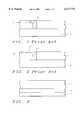
- FIGS. 1 and 2are schematic cross-sectional representations illustrating problems in the prior art.
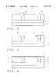
- FIGS. 3 through 10are schematic cross-sectional representations of a preferred embodiment of the present invention.
- the process of the present inventionintegrates formation of a MOM capacitor with a dual damascene process while avoiding the problem of dishing.
- the capacitor sizeis not limited by the metal line.
- FIGS. 1 and 2illustrate the problems involved in using a dual damascene method to form a MOM capacitor.
- a dual damascene openinghas been formed in a dielectric layer 17 on a semiconductor substrate 10.
- the openingis filled with copper 19.
- the horizontal portion 21will form the bottom capacitor plate.
- the width of the capacitor plate 21must be increased to increase capacitance. If the width of the upper portion of the dual damascene opening is increased, as shown in FIG. 2, dishing 23 will occur after polishing of the copper layer 21.
- the semiconductor substrate 10is preferably composed of silicon having a (100) crystallographic orientation.
- Semiconductor device structuresare formed in and on the semiconductor substrate. These may include gate electrodes and interconnection lines and associated source and drain regions and lower levels of metallization.
- the semiconductor device structures, not shown,may be formed in layer 14 and covered with an insulating layer.
- a dielectric layer 20is formed over the layer 14. This may be a multi-layer of alternating dielectric and etch stop layers, depending upon the particular method to be used to form the dual damascene opening. Typical dielectric materials include tetraethoxysilane (TEOS) oxide, fluorinated silicate glass (FSG), or other low dielectric constant materials.
- TEOStetraethoxysilane
- FSGfluorinated silicate glass
- the total thickness of the layer 20is between about 10,000 and 20,000 Angstroms.
- dual damascene openings 22are formed using one of the conventional dual damascene processes, such as trench first, via first, or trench through.
- the dual damascene openings 22have a conventional upper width A of between about 3000 and 10,000 Angstroms, as the width shown in FIG. 1 of the prior art. Because of this small width, dishing will not be a problem.
- the dual damascene openingsare filled with copper using, for example, a copper seed layer and electroless plating, electrochemical plating, or copper deposition, or the like. If necessary, excess copper is polished back, using, for example, chemical mechanical polishing. Because the width A is not too wide, dishing (as shown in FIG. 2) does not occur.
- the completed copper damascene regions 24/26are shown in FIG. 5. 24 is the via portion and 26 is the metal line portion of the copper regions.
- the metal line portion 26 of the copper damascene regionis not wide enough to form a high quality bottom capacitor plate. Therefore, an additional thin metal layer 30 is deposited over the metal lines 26 and the dielectric layer 20, as shown in FIG. 6.
- the metal layer 30may comprise tantalum nitride or titanium nitride or any other metal.
- the metal layer 30is deposited by physical vapor deposition or chemical vapor deposition to a thickness of between about 1000 and 3000 Angstroms.
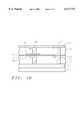
- the metal layer 30is patterned using conventional lithographic and etching techniques to form the bottom capacitor plate 32 contacting one of the copper lines 26, as shown in FIG. 7.
- the bottom plate 32can be formed in any size needed.
- the capacitor sizeis not limited by the size of the copper line bottom contact 26.
- a capacitor dielectric layer 34is deposited over the bottom capacitor plate 32.
- the capacitor dielectricmay comprises silicon nitride, silicon oxynitride, ONO (oxide/nitride/oxide), NO (nitride/oxide), or any other suitable dielectric.
- the thickness of the capacitor dielectric layer 34is typically between about 500 and 2000 Angstroms.
- a second metal layeris deposited over the capacitor dielectric layer and patterned to form the top capacitor plate 38.
- the second metal layermay comprise tantalum nitride or any other suitable metal and have a thickness of between about 1000 and 3000 Angstroms.
- a second dielectric layer 44is deposited over the capacitor 40 and capacitor dielectric 34. Again, this layer 44 may comprise multiple layers. Dual damascene openings may be formed in this dielectric layer and filled with copper 48, as shown. If this is the topmost metal layer, a passivation layer 50 completes the integrated circuit.
- the MOM capacitoris formed in the second to topmost layer in order to prevent capacitive loss to the substrate. It will be understood by those skilled in the art, however, that the MOM capacitor may be fabricated according to the process of the invention in any of the metal layers.
- the process of the inventionresults in the fabrication of a metal-oxide-metal capacitor using a dual damascene process. Dishing does not occur since the dual damascene opening is kept narrow enough.
- the additional thin metal layerprovides the increased width of the bottom capacitor plate required to increase capacitance without increasing the width of the dual damascene opening.
Landscapes
- Engineering & Computer Science (AREA)
- Physics & Mathematics (AREA)
- Condensed Matter Physics & Semiconductors (AREA)
- General Physics & Mathematics (AREA)
- Manufacturing & Machinery (AREA)
- Computer Hardware Design (AREA)
- Microelectronics & Electronic Packaging (AREA)
- Power Engineering (AREA)
- Internal Circuitry In Semiconductor Integrated Circuit Devices (AREA)
Abstract
Description
(1) Field of the Invention
The present invention relates to a method of fabricating a metal-oxide-metal capacitor, and more particularly, to a method of integrating the formation of a metal-oxide-metal capacitor into the dual damascene process in the fabrication of an integrated circuit device.
(2) Description of the Art
Capacitors are critical components in the integrated circuit devices of today. Both polysilicon and metal-oxide-metal capacitors have been used in the art. Metal-oxide-metal (MOM) capacitors have been increasing in popularity because their minimal capacitive loss to the substrate results in a high quality capacitor. It is desired to integrate the MOM capacitor with the dual copper damascene process, for example, in RF/Mixed signal applications where the capacitor is to be used as a decoupler or filter. The major concerns involved in integrating the MOM capacitor in the dual damascene process include: a) dishing effect if the metal width is too great and b) area capacitor size is limited by the metal line.
U.S. Pat. No. 5,813,664 to Pan teaches a process where the bottom capacitor plate and bond pads are formed at the same time. U.S. Pat. No. 5,736,448 to Saia et al show a MOM capacitor on an upper level. U.S. Pat. No. 5,479,316 to Smrtic et al, U.S. Pat. No. 5,812,364 to Oku et al, and U.S. Pat. No. 5,406,447 to Miyazaki all disclose various methods of forming metal-oxide-metal capacitors.
Accordingly, it is a primary object of the invention to provide an effective and very manufacturable process for fabricating a metal-oxide-metal capacitor using a dual damascene process.
Another object of the present invention is to provide a method for fabricating a metal-oxide-metal capacitor using a dual damascene process wherein an additional thin metal layer forms the bottom capacitor plate.
In accordance with the objects of this invention, a method for fabricating a metal-oxide-metal capacitor using a dual damascene process is achieved. A dielectric layer is provided overlying a semiconductor substrate. A dual damascene opening in the dielectric layer is filled with copper to form a copper via underlying a copper line. A first metal layer is deposited overlying the copper line and patterned to form a bottom capacitor plate contacting the copper line. A capacitor dielectric layer is deposited overlying the bottom capacitor plate. A second metal layer is deposited overlying the capacitor dielectric layer and patterned to form a top capacitor plate to complete fabrication of a metal-oxide-metal capacitor.
In the following drawings forming a material part of this description, there is shown:
FIGS. 1 and 2 are schematic cross-sectional representations illustrating problems in the prior art.
FIGS. 3 through 10 are schematic cross-sectional representations of a preferred embodiment of the present invention.
The process of the present invention integrates formation of a MOM capacitor with a dual damascene process while avoiding the problem of dishing. In this process, the capacitor size is not limited by the metal line.
FIGS. 1 and 2 illustrate the problems involved in using a dual damascene method to form a MOM capacitor. As shown in FIG. 1, a dual damascene opening has been formed in adielectric layer 17 on asemiconductor substrate 10. The opening is filled withcopper 19. Thehorizontal portion 21 will form the bottom capacitor plate. However, the width of thecapacitor plate 21 must be increased to increase capacitance. If the width of the upper portion of the dual damascene opening is increased, as shown in FIG. 2,dishing 23 will occur after polishing of thecopper layer 21.
The process of the present invention to avoid these problems will now be described with reference to FIGS. 3-10. Referring now more particularly to FIG. 3, there is shown a partially completed integrated circuit device. Thesemiconductor substrate 10 is preferably composed of silicon having a (100) crystallographic orientation. Semiconductor device structures are formed in and on the semiconductor substrate. These may include gate electrodes and interconnection lines and associated source and drain regions and lower levels of metallization. The semiconductor device structures, not shown, may be formed inlayer 14 and covered with an insulating layer.
Now, adielectric layer 20 is formed over thelayer 14. This may be a multi-layer of alternating dielectric and etch stop layers, depending upon the particular method to be used to form the dual damascene opening. Typical dielectric materials include tetraethoxysilane (TEOS) oxide, fluorinated silicate glass (FSG), or other low dielectric constant materials. The total thickness of thelayer 20 is between about 10,000 and 20,000 Angstroms.
As shown in FIG. 4, dualdamascene openings 22 are formed using one of the conventional dual damascene processes, such as trench first, via first, or trench through. Thedual damascene openings 22 have a conventional upper width A of between about 3000 and 10,000 Angstroms, as the width shown in FIG. 1 of the prior art. Because of this small width, dishing will not be a problem.
The dual damascene openings are filled with copper using, for example, a copper seed layer and electroless plating, electrochemical plating, or copper deposition, or the like. If necessary, excess copper is polished back, using, for example, chemical mechanical polishing. Because the width A is not too wide, dishing (as shown in FIG. 2) does not occur. The completed copperdamascene regions 24/26 are shown in FIG. 5. 24 is the via portion and 26 is the metal line portion of the copper regions.
Now, the key feature of the present invention will be described. Themetal line portion 26 of the copper damascene region is not wide enough to form a high quality bottom capacitor plate. Therefore, an additionalthin metal layer 30 is deposited over themetal lines 26 and thedielectric layer 20, as shown in FIG. 6. Themetal layer 30 may comprise tantalum nitride or titanium nitride or any other metal. Themetal layer 30 is deposited by physical vapor deposition or chemical vapor deposition to a thickness of between about 1000 and 3000 Angstroms.
Now, themetal layer 30 is patterned using conventional lithographic and etching techniques to form thebottom capacitor plate 32 contacting one of thecopper lines 26, as shown in FIG. 7. Thebottom plate 32 can be formed in any size needed. Thus, the capacitor size is not limited by the size of the copperline bottom contact 26.
Referring now to FIG. 8, acapacitor dielectric layer 34 is deposited over thebottom capacitor plate 32. The capacitor dielectric may comprises silicon nitride, silicon oxynitride, ONO (oxide/nitride/oxide), NO (nitride/oxide), or any other suitable dielectric. The thickness of thecapacitor dielectric layer 34 is typically between about 500 and 2000 Angstroms.
Next, as shown in FIG. 9, a second metal layer is deposited over the capacitor dielectric layer and patterned to form thetop capacitor plate 38. The second metal layer may comprise tantalum nitride or any other suitable metal and have a thickness of between about 1000 and 3000 Angstroms.
This completes theMOM capacitor 40, shown in FIG. 10. Now, asecond dielectric layer 44 is deposited over thecapacitor 40 andcapacitor dielectric 34. Again, thislayer 44 may comprise multiple layers. Dual damascene openings may be formed in this dielectric layer and filled withcopper 48, as shown. If this is the topmost metal layer, apassivation layer 50 completes the integrated circuit.
In the example illustrated, the MOM capacitor is formed in the second to topmost layer in order to prevent capacitive loss to the substrate. It will be understood by those skilled in the art, however, that the MOM capacitor may be fabricated according to the process of the invention in any of the metal layers.
The process of the invention results in the fabrication of a metal-oxide-metal capacitor using a dual damascene process. Dishing does not occur since the dual damascene opening is kept narrow enough. The additional thin metal layer provides the increased width of the bottom capacitor plate required to increase capacitance without increasing the width of the dual damascene opening.
While the invention has been particularly shown and described with reference to the preferred embodiments thereof, it will be understood by those skilled in the art that various changes in form and details may be made without departing from the spirit and scope of the invention.
Claims (20)
1. A method for fabricating a metal-oxide-metal capacitor comprising:
providing a dielectric layer overlying a semiconductor substrate;
filling a dual damascene opening within said dielectric layer with copper to form a copper via underlying a copper line;
depositing a first metal layer overlying said copper line;
patterning said first metal layer to form a bottom capacitor plate contacting said copper line;
depositing a capacitor dielectric layer overlying said bottom capacitor plate; and
depositing a second metal layer overlying said capacitor dielectric layer and patterning said second metal layer to form a top capacitor plate to complete said fabrication of said metal-oxide-metal capacitor.
2. The method according to claim 1 wherein said semiconductor substrate includes semiconductor device structures such as gate electrodes and source and drain regions.
3. The method according to claim 1 wherein said semiconductor substrate includes semiconductor device structures such as gate electrodes and source and drain regions and multiple levels of metal interconnections.
4. The method according to claim 1 wherein said first metal layer comprises tantalum nitride.
5. The method according to claim 1 wherein said first metal layer comprises titanium nitride.
6. The method according to claim 1 wherein said capacitor dielectric layer comprises silicon nitride having a thickness of between about 500 and 2000 Angstroms.
7. The method according to claim 1 wherein said capacitor dielectric layer comprises silicon oxynitride having a thickness of between about 500 and 2000 Angstroms.
8. The method according to claim 1 wherein said second metal layer comprises tantalum nitride.
9. A method for fabricating a metal-oxide-metal capacitor comprising:
providing a dielectric layer overlying a semiconductor substrate;
filling a dual damascene opening within said dielectric layer with copper to form a copper via underlying a copper line;
depositing a first tantalum nitride layer overlying said copper line;
patterning said first tantalum nitride layer to form a bottom capacitor plate contacting said copper line;
depositing a capacitor dielectric layer overlying said bottom capacitor plate; and
depositing a second tantalum nitride layer overlying said capacitor dielectric layer and patterning said second tantalum nitride layer to form a top capacitor plate to complete said fabrication of said metal-oxide-metal capacitor.
10. The method according to claim 9 wherein said semiconductor substrate includes semiconductor device structures such as gate electrodes and source and drain regions.
11. The method according to claim 9 wherein said semiconductor substrate includes semiconductor device structures such as gate electrodes and source and drain regions and multiple levels of metal interconnections.
12. The method according to claim 9 wherein said capacitor dielectric layer comprises silicon nitride having a thickness of between about 500 and 2000 Angstroms.
13. The method according to claim 9 wherein said capacitor dielectric layer comprises silicon oxynitride having a thickness of between about 500 and 2000 Angstroms.
14. A method for fabricating a metal-oxide-metal capacitor in the fabrication of an integrated circuit comprising:
providing a first dielectric layer overlying a semiconductor substrate;
filling a dual damascene opening within said first dielectric layer with copper to form a copper via underlying a copper line;
depositing a first metal layer overlying said copper line;
patterning said first metal layer to form a bottom capacitor plate contacting said copper line;
depositing a capacitor dielectric layer overlying said bottom capacitor plate;
depositing a second metal layer overlying said capacitor dielectric layer and patterning said second metal layer to form a top capacitor plate to complete said fabrication of said metal-oxide-metal capacitor;
depositing a second dielectric layer over said metal-oxide-metal capacitor;
forming a dual damascene opening in said second dielectric layer to contact said top capacitor plate and filling said dual damascene opening with copper; and
depositing a passivation layer over said second dielectric layer to complete fabrication of said integrated circuit.
15. The method according to claim 14 wherein said semiconductor substrate includes semiconductor device structures such as gate electrodes and source and drain regions.
16. The method according to claim 14 wherein said semiconductor substrate includes semiconductor device structures such as gate electrodes and source and drain regions and multiple levels of metal interconnections.
17. The method according to claim 14 wherein said first metal layer comprises one of the group containing tantalum nitride and titanium nitride.
18. The method according to claim 14 wherein said capacitor dielectric layer comprises silicon nitride having a thickness of between about 500 and 2000 Angstroms.
19. The method according to claim 14 wherein said capacitor dielectric layer comprises silicon oxynitride having a thickness of between about 500 and 2000 Angstroms.
20. The method according to claim 14 wherein said second metal layer comprises tantalum nitride.
Priority Applications (2)
| Application Number | Priority Date | Filing Date | Title |
|---|---|---|---|
| US09/435,436US6117747A (en) | 1999-11-22 | 1999-11-22 | Integration of MOM capacitor into dual damascene process |
| SG200002959ASG115338A1 (en) | 1999-11-22 | 2000-05-31 | Integration of mom capacitor into dual damascene process |
Applications Claiming Priority (1)
| Application Number | Priority Date | Filing Date | Title |
|---|---|---|---|
| US09/435,436US6117747A (en) | 1999-11-22 | 1999-11-22 | Integration of MOM capacitor into dual damascene process |
Publications (1)
| Publication Number | Publication Date |
|---|---|
| US6117747Atrue US6117747A (en) | 2000-09-12 |
Family
ID=23728386
Family Applications (1)
| Application Number | Title | Priority Date | Filing Date |
|---|---|---|---|
| US09/435,436Expired - LifetimeUS6117747A (en) | 1999-11-22 | 1999-11-22 | Integration of MOM capacitor into dual damascene process |
Country Status (2)
| Country | Link |
|---|---|
| US (1) | US6117747A (en) |
| SG (1) | SG115338A1 (en) |
Cited By (33)
| Publication number | Priority date | Publication date | Assignee | Title |
|---|---|---|---|---|
| US6436787B1 (en) | 2001-07-26 | 2002-08-20 | Taiwan Semiconductor Manufacturing Company | Method of forming crown-type MIM capacitor integrated with the CU damascene process |
| US6500724B1 (en) | 2000-08-21 | 2002-12-31 | Motorola, Inc. | Method of making semiconductor device having passive elements including forming capacitor electrode and resistor from same layer of material |
| US6534374B2 (en) | 2001-06-07 | 2003-03-18 | Institute Of Microelectronics | Single damascene method for RF IC passive component integration in copper interconnect process |
| US6579787B2 (en)* | 2000-08-09 | 2003-06-17 | Mitsubishi Denki Kabushiki Kaisha | Semiconductor device with a fluorinated silicate glass film as an interlayer metal dielectric film, and manufacturing method thereof |
| EP1328973A2 (en)* | 2000-10-03 | 2003-07-23 | Broadcom Corporation | High-density metal capacitor using dual-damascene copper interconnect |
| US6624040B1 (en) | 2002-09-20 | 2003-09-23 | Chartered Semiconductor Manufacturing Ltd. | Self-integrated vertical MIM capacitor in the dual damascene process |
| US20030203586A1 (en)* | 2001-01-17 | 2003-10-30 | Volant Richard P. | Production of metal insulator metal (MIM) structures using anodizing process |
| US20030211731A1 (en)* | 2002-05-07 | 2003-11-13 | Chartered Semiconductor Manufacturing Ltd. | Metal sandwich structure for MIM capacitor onto dual damascene |
| US6680542B1 (en)* | 2000-05-18 | 2004-01-20 | Agere Systems Inc. | Damascene structure having a metal-oxide-metal capacitor associated therewith |
| US6709918B1 (en)* | 2002-12-02 | 2004-03-23 | Chartered Semiconductor Manufacturing Ltd. | Method for making a metal-insulator-metal (MIM) capacitor and metal resistor for a copper back-end-of-line (BEOL) technology |
| US20040058547A1 (en)* | 2002-09-25 | 2004-03-25 | Xiaorong Morrow | Method and apparatus for forming metal-metal oxide etch stop/barrier for integrated circuit interconnects |
| US6723600B2 (en) | 2001-04-18 | 2004-04-20 | International Business Machines Corporation | Method for making a metal-insulator-metal capacitor using plate-through mask techniques |
| US20040137692A1 (en)* | 2002-12-24 | 2004-07-15 | Nam Sang Woo | Methods for forming capacitors and contact holes of semiconductor devices simultaneously |
| US6767788B2 (en) | 2001-06-12 | 2004-07-27 | Hynix Semiconductor Inc. | Semiconductor device having a metal insulator metal capacitor |
| US20040164339A1 (en)* | 2003-02-20 | 2004-08-26 | Infineon Technologies North America Corp. | Capacitor and method of manufacturing a capacitor |
| WO2004032236A3 (en)* | 2002-09-30 | 2004-10-28 | Intel Corp | Method and apparatus to fabricate an on-chip decoupling capacitor |
| US6830971B2 (en) | 2002-11-02 | 2004-12-14 | Chartered Semiconductor Manufacturing Ltd | High K artificial lattices for capacitor applications to use in CU or AL BEOL |
| US20050074149A1 (en)* | 2003-10-03 | 2005-04-07 | Confirma, Inc. | System and method for hierarchical analysis of contrast enhanced medical imaging information |
| US20050093093A1 (en)* | 2003-10-30 | 2005-05-05 | Edmund Burke | Capacitor integration at top-metal level with a protective cladding for copper surface protection |
| US6919244B1 (en) | 2004-03-10 | 2005-07-19 | Motorola, Inc. | Method of making a semiconductor device, and semiconductor device made thereby |
| US20060220104A1 (en)* | 2005-03-31 | 2006-10-05 | Sanyo Electric Co., Ltd. | Semiconductor device and method for manufacturing the same |
| US20070045774A1 (en)* | 2005-08-26 | 2007-03-01 | Texas Instruments Incorporated | TaN integrated circuit (IC) capacitor |
| US20070158783A1 (en)* | 2006-01-09 | 2007-07-12 | Yueh-You Chen | Interdigitated capacitive structure for an integrated circuit |
| US20070235838A1 (en)* | 2006-03-28 | 2007-10-11 | Taiwan Semiconductor Manufacturing Company, Ltd. | Flexible metal-oxide-metal capacitor design |
| US20080001300A1 (en)* | 2000-10-18 | 2008-01-03 | Megica Corporation | Post passivation interconnection schemes on top of IC chip |
| US20080001256A1 (en)* | 2005-06-09 | 2008-01-03 | Freescale Semiconductors, Inc. | Semiconductor device comprising passive components |
| US20080265369A1 (en)* | 2007-04-30 | 2008-10-30 | Taiwan Semiconductor Manufacturing Co., Ltd. | Semiconductor Capacitor Structure |
| US20090224359A1 (en)* | 2008-03-10 | 2009-09-10 | Chung-Long Chang | MOM Capacitors Integrated with Air-Gaps |
| US20100032803A1 (en)* | 2008-08-08 | 2010-02-11 | Texas Instruments Incorporated | Capacitor contact formed concurrently with bond pad metallization |
| US20110284990A1 (en)* | 2010-04-30 | 2011-11-24 | Silterra Malaysia Sdn Bhd | Process for making an alignment structure in the fabrication of a semiconductor device |
| US20150044848A1 (en)* | 2013-08-06 | 2015-02-12 | Texas Instruments Incorporated | High voltage hybrid polymeric-ceramic dielectric capacitor |
| US10734444B1 (en) | 2019-01-28 | 2020-08-04 | Globalfoundries Singapore Pte. Ltd. | Integrated circuits with integrated memory structures and capacitors and methods for fabricating the same |
| WO2021067188A1 (en) | 2019-09-30 | 2021-04-08 | Texas Instruments Incorporated | Integrated capacitor with extended head bump bond pillar |
Citations (6)
| Publication number | Priority date | Publication date | Assignee | Title |
|---|---|---|---|---|
| US5406447A (en)* | 1992-01-06 | 1995-04-11 | Nec Corporation | Capacitor used in an integrated circuit and comprising opposing electrodes having barrier metal films in contact with a dielectric film |
| US5479316A (en)* | 1993-08-24 | 1995-12-26 | Analog Devices, Inc. | Integrated circuit metal-oxide-metal capacitor and method of making same |
| US5736448A (en)* | 1995-12-04 | 1998-04-07 | General Electric Company | Fabrication method for thin film capacitors |
| US5812364A (en)* | 1996-07-03 | 1998-09-22 | Mitsubishi Denki Kabushiki Kaisha | Capacitor |
| US5813664A (en)* | 1995-10-19 | 1998-09-29 | Chartered Semiconductor Manufacturing Ltd. | Back-end capacitor with high unit capacitance |
| US5946567A (en)* | 1998-03-20 | 1999-08-31 | Taiwan Semiconductor Manufacturing Company, Ltd. | Method for making metal capacitors for deep submicrometer processes for semiconductor integrated circuits |
- 1999
- 1999-11-22USUS09/435,436patent/US6117747A/ennot_activeExpired - Lifetime
- 2000
- 2000-05-31SGSG200002959Apatent/SG115338A1/enunknown
Patent Citations (6)
| Publication number | Priority date | Publication date | Assignee | Title |
|---|---|---|---|---|
| US5406447A (en)* | 1992-01-06 | 1995-04-11 | Nec Corporation | Capacitor used in an integrated circuit and comprising opposing electrodes having barrier metal films in contact with a dielectric film |
| US5479316A (en)* | 1993-08-24 | 1995-12-26 | Analog Devices, Inc. | Integrated circuit metal-oxide-metal capacitor and method of making same |
| US5813664A (en)* | 1995-10-19 | 1998-09-29 | Chartered Semiconductor Manufacturing Ltd. | Back-end capacitor with high unit capacitance |
| US5736448A (en)* | 1995-12-04 | 1998-04-07 | General Electric Company | Fabrication method for thin film capacitors |
| US5812364A (en)* | 1996-07-03 | 1998-09-22 | Mitsubishi Denki Kabushiki Kaisha | Capacitor |
| US5946567A (en)* | 1998-03-20 | 1999-08-31 | Taiwan Semiconductor Manufacturing Company, Ltd. | Method for making metal capacitors for deep submicrometer processes for semiconductor integrated circuits |
Cited By (72)
| Publication number | Priority date | Publication date | Assignee | Title |
|---|---|---|---|---|
| US20060081992A1 (en)* | 2000-03-12 | 2006-04-20 | Renesas Technology Corp | Semiconductor device with a fluorinated silicate glass film as an interlayer metal dielectric film, and manufacturing method thereof |
| US6680542B1 (en)* | 2000-05-18 | 2004-01-20 | Agere Systems Inc. | Damascene structure having a metal-oxide-metal capacitor associated therewith |
| US7012336B2 (en) | 2000-08-09 | 2006-03-14 | Renesas Technology Corp. | Semiconductor device with a fluorinated silicate glass film as an interlayer metal dielectric film, and manufacturing method thereof |
| US6579787B2 (en)* | 2000-08-09 | 2003-06-17 | Mitsubishi Denki Kabushiki Kaisha | Semiconductor device with a fluorinated silicate glass film as an interlayer metal dielectric film, and manufacturing method thereof |
| US20030211721A1 (en)* | 2000-08-09 | 2003-11-13 | Mitsubishi Denki Kabushiki Kaisha | Semiconductor device with a fluorinated silicate glass film as an interlayer metal dielectric film, and manufacturing method thereof |
| US6500724B1 (en) | 2000-08-21 | 2002-12-31 | Motorola, Inc. | Method of making semiconductor device having passive elements including forming capacitor electrode and resistor from same layer of material |
| US6825092B2 (en) | 2000-08-21 | 2004-11-30 | Freescale Semiconductor, Inc. | Semiconductor device having passive elements and method of making same |
| EP1328973A2 (en)* | 2000-10-03 | 2003-07-23 | Broadcom Corporation | High-density metal capacitor using dual-damascene copper interconnect |
| US20080042293A1 (en)* | 2000-10-18 | 2008-02-21 | Megica Corporation | Post passivation interconnection schemes on top of IC chip |
| US20080045002A1 (en)* | 2000-10-18 | 2008-02-21 | Megica Corporation | Post passivation interconnection schemes on top of IC chip |
| US20080042294A1 (en)* | 2000-10-18 | 2008-02-21 | Megica Corporation | Post passivation interconnection schemes on top of IC chip |
| US20080042285A1 (en)* | 2000-10-18 | 2008-02-21 | Megica Corporation | Post passivation interconnection schemes on top of IC chip |
| US8461686B2 (en) | 2000-10-18 | 2013-06-11 | Megica Corporation | Post passivation interconnection schemes on top of IC chip |
| US8004088B2 (en) | 2000-10-18 | 2011-08-23 | Megica Corporation | Post passivation interconnection schemes on top of IC chip |
| US8435883B2 (en) | 2000-10-18 | 2013-05-07 | Megica Corporation | Post passivation interconnection schemes on top of IC chips |
| US20080001300A1 (en)* | 2000-10-18 | 2008-01-03 | Megica Corporation | Post passivation interconnection schemes on top of IC chip |
| US8492900B2 (en) | 2000-10-18 | 2013-07-23 | Megica Corporation | Post passivation interconnection schemes on top of IC chip |
| US8482127B2 (en) | 2000-10-18 | 2013-07-09 | Megica Corporation | Post passivation interconnection schemes on top of IC chip |
| US8188603B2 (en) | 2000-10-18 | 2012-05-29 | Megica Corporation | Post passivation interconnection schemes on top of IC chip |
| US20030203586A1 (en)* | 2001-01-17 | 2003-10-30 | Volant Richard P. | Production of metal insulator metal (MIM) structures using anodizing process |
| US6992368B2 (en)* | 2001-01-17 | 2006-01-31 | International Business Machines Corporation | Production of metal insulator metal (MIM) structures using anodizing process |
| US6723600B2 (en) | 2001-04-18 | 2004-04-20 | International Business Machines Corporation | Method for making a metal-insulator-metal capacitor using plate-through mask techniques |
| US6534374B2 (en) | 2001-06-07 | 2003-03-18 | Institute Of Microelectronics | Single damascene method for RF IC passive component integration in copper interconnect process |
| US20040232557A1 (en)* | 2001-06-12 | 2004-11-25 | Hynix Semiconductor Inc. | Semiconductor device having a metal insulator metal capacitor |
| US6767788B2 (en) | 2001-06-12 | 2004-07-27 | Hynix Semiconductor Inc. | Semiconductor device having a metal insulator metal capacitor |
| US6436787B1 (en) | 2001-07-26 | 2002-08-20 | Taiwan Semiconductor Manufacturing Company | Method of forming crown-type MIM capacitor integrated with the CU damascene process |
| US6746914B2 (en)* | 2002-05-07 | 2004-06-08 | Chartered Semiconductor Manufacturing Ltd. | Metal sandwich structure for MIM capacitor onto dual damascene |
| US20030211731A1 (en)* | 2002-05-07 | 2003-11-13 | Chartered Semiconductor Manufacturing Ltd. | Metal sandwich structure for MIM capacitor onto dual damascene |
| US6624040B1 (en) | 2002-09-20 | 2003-09-23 | Chartered Semiconductor Manufacturing Ltd. | Self-integrated vertical MIM capacitor in the dual damascene process |
| US20040058547A1 (en)* | 2002-09-25 | 2004-03-25 | Xiaorong Morrow | Method and apparatus for forming metal-metal oxide etch stop/barrier for integrated circuit interconnects |
| WO2004032236A3 (en)* | 2002-09-30 | 2004-10-28 | Intel Corp | Method and apparatus to fabricate an on-chip decoupling capacitor |
| US7095073B2 (en) | 2002-11-02 | 2006-08-22 | Chartered Semiconductor Manufacturing Ltd. | High K artificial lattices for capacitor applications to use in Cu or Al BEOL |
| US20050118780A1 (en)* | 2002-11-02 | 2005-06-02 | Chartered Semiconductor Manufacturing Ltd. | High K artificial lattices for capacitor applications to use in Cu or Al BEOL |
| US6830971B2 (en) | 2002-11-02 | 2004-12-14 | Chartered Semiconductor Manufacturing Ltd | High K artificial lattices for capacitor applications to use in CU or AL BEOL |
| US6709918B1 (en)* | 2002-12-02 | 2004-03-23 | Chartered Semiconductor Manufacturing Ltd. | Method for making a metal-insulator-metal (MIM) capacitor and metal resistor for a copper back-end-of-line (BEOL) technology |
| US20040137692A1 (en)* | 2002-12-24 | 2004-07-15 | Nam Sang Woo | Methods for forming capacitors and contact holes of semiconductor devices simultaneously |
| US7153752B2 (en)* | 2002-12-24 | 2006-12-26 | Dongbu Electronics, Co., Ltd. | Methods for forming capacitors and contact holes of semiconductor devices simultaneously |
| US20070294871A1 (en)* | 2003-02-20 | 2007-12-27 | Petra Felsner | Capacitor and Method of Manufacturing a Capacitor |
| CN1751367B (en)* | 2003-02-20 | 2010-06-16 | 因芬尼昂技术股份公司 | Capacitor and method of manufacturing capacitor |
| US7615440B2 (en) | 2003-02-20 | 2009-11-10 | Infineon Technologies Ag | Capacitor and method of manufacturing a capacitor |
| US7268383B2 (en) | 2003-02-20 | 2007-09-11 | Infineon Technologies Ag | Capacitor and method of manufacturing a capacitor |
| US20040164339A1 (en)* | 2003-02-20 | 2004-08-26 | Infineon Technologies North America Corp. | Capacitor and method of manufacturing a capacitor |
| WO2004075218A1 (en)* | 2003-02-20 | 2004-09-02 | Infineon Technologies Ag | Capacitor, semiconductor device with a capacitor and method of manufactuing thereof |
| US20050074149A1 (en)* | 2003-10-03 | 2005-04-07 | Confirma, Inc. | System and method for hierarchical analysis of contrast enhanced medical imaging information |
| US20050093093A1 (en)* | 2003-10-30 | 2005-05-05 | Edmund Burke | Capacitor integration at top-metal level with a protective cladding for copper surface protection |
| US8604587B2 (en) | 2003-10-30 | 2013-12-10 | Texas Instruments Incorporated | Capacitor integration at top-metal level with a protective cladding for copper surface protection |
| US7674682B2 (en)* | 2003-10-30 | 2010-03-09 | Texas Instruments Incorporated | Capacitor integration at top-metal level with a protective cladding for copper surface protection |
| US20100117195A1 (en)* | 2003-10-30 | 2010-05-13 | Texas Instruments Incorporated | Capacitor integration at top-metal level with a protective cladding for copper surface protection |
| US6919244B1 (en) | 2004-03-10 | 2005-07-19 | Motorola, Inc. | Method of making a semiconductor device, and semiconductor device made thereby |
| US20060220104A1 (en)* | 2005-03-31 | 2006-10-05 | Sanyo Electric Co., Ltd. | Semiconductor device and method for manufacturing the same |
| US7535079B2 (en) | 2005-06-09 | 2009-05-19 | Freescale Semiconductor, Inc. | Semiconductor device comprising passive components |
| US20080001256A1 (en)* | 2005-06-09 | 2008-01-03 | Freescale Semiconductors, Inc. | Semiconductor device comprising passive components |
| US7573086B2 (en)* | 2005-08-26 | 2009-08-11 | Texas Instruments Incorporated | TaN integrated circuit (IC) capacitor |
| US20070045774A1 (en)* | 2005-08-26 | 2007-03-01 | Texas Instruments Incorporated | TaN integrated circuit (IC) capacitor |
| US8169014B2 (en) | 2006-01-09 | 2012-05-01 | Taiwan Semiconductor Manufacturing Co., Ltd. | Interdigitated capacitive structure for an integrated circuit |
| US20070158783A1 (en)* | 2006-01-09 | 2007-07-12 | Yueh-You Chen | Interdigitated capacitive structure for an integrated circuit |
| US20070235838A1 (en)* | 2006-03-28 | 2007-10-11 | Taiwan Semiconductor Manufacturing Company, Ltd. | Flexible metal-oxide-metal capacitor design |
| US7485912B2 (en) | 2006-03-28 | 2009-02-03 | Taiwan Semiconductor Manufacturing Company, Ltd. | Flexible metal-oxide-metal capacitor design |
| US20080265369A1 (en)* | 2007-04-30 | 2008-10-30 | Taiwan Semiconductor Manufacturing Co., Ltd. | Semiconductor Capacitor Structure |
| US9177908B2 (en) | 2007-04-30 | 2015-11-03 | Taiwan Semiconductor Manufacturing Company, Limited | Stacked semiconductor capacitor structure |
| US20090224359A1 (en)* | 2008-03-10 | 2009-09-10 | Chung-Long Chang | MOM Capacitors Integrated with Air-Gaps |
| US8053865B2 (en) | 2008-03-10 | 2011-11-08 | Taiwan Semiconductor Manufacturing Company, Ltd. | MOM capacitors integrated with air-gaps |
| US8431463B2 (en)* | 2008-08-08 | 2013-04-30 | Texas Instruments Incorporated | Capacitor contact formed concurrently with bond pad metallization |
| US20100032803A1 (en)* | 2008-08-08 | 2010-02-11 | Texas Instruments Incorporated | Capacitor contact formed concurrently with bond pad metallization |
| US20110284990A1 (en)* | 2010-04-30 | 2011-11-24 | Silterra Malaysia Sdn Bhd | Process for making an alignment structure in the fabrication of a semiconductor device |
| US20150044848A1 (en)* | 2013-08-06 | 2015-02-12 | Texas Instruments Incorporated | High voltage hybrid polymeric-ceramic dielectric capacitor |
| US9006074B2 (en)* | 2013-08-06 | 2015-04-14 | Texas Instruments Incorporated | High voltage hybrid polymeric-ceramic dielectric capacitor |
| US10734444B1 (en) | 2019-01-28 | 2020-08-04 | Globalfoundries Singapore Pte. Ltd. | Integrated circuits with integrated memory structures and capacitors and methods for fabricating the same |
| WO2021067188A1 (en) | 2019-09-30 | 2021-04-08 | Texas Instruments Incorporated | Integrated capacitor with extended head bump bond pillar |
| US11094620B2 (en) | 2019-09-30 | 2021-08-17 | Texas Instruments Incorporated | Integrated capacitor with extended head bump bond pillar |
| EP4038658A4 (en)* | 2019-09-30 | 2023-04-12 | Texas Instruments Incorporated | INTEGRATED CAPACITOR WITH EXTENDED HEAD BUDGE TERMINAL |
| US11810843B2 (en) | 2019-09-30 | 2023-11-07 | Texas Instruments Incorporated | Integrated capacitor with extended head bump bond pillar |
Also Published As
| Publication number | Publication date |
|---|---|
| SG115338A1 (en) | 2005-10-28 |
Similar Documents
| Publication | Publication Date | Title |
|---|---|---|
| US6117747A (en) | Integration of MOM capacitor into dual damascene process | |
| US6300682B2 (en) | High performance MIM (MIP) IC capacitor process | |
| US7436016B2 (en) | MIM capacitor with a cap layer over the conductive plates | |
| US6593185B1 (en) | Method of forming embedded capacitor structure applied to logic integrated circuit | |
| US6436787B1 (en) | Method of forming crown-type MIM capacitor integrated with the CU damascene process | |
| US7462535B2 (en) | Semiconductor device with analog capacitor and method of fabricating the same | |
| US9269762B2 (en) | Metal-insulator-metal (MIM) capacitor within topmost thick inter-metal dielectric layers | |
| US6329234B1 (en) | Copper process compatible CMOS metal-insulator-metal capacitor structure and its process flow | |
| US6670237B1 (en) | Method for an advanced MIM capacitor | |
| CN100365765C (en) | Metal-insulator-metal capacitor structure and manufacturing method in dual damascene structure | |
| US6437365B1 (en) | Raised tungsten plug antifuse and fabrication processes | |
| US7517763B2 (en) | Semiconductor device having fuse and capacitor at the same level and method of fabricating the same | |
| KR100429726B1 (en) | A capacitor for integration with copper damascene processes and a method of manufacture therefore | |
| US20080232025A1 (en) | Mim capacitor and method of making same | |
| US20030040161A1 (en) | Method of producing an integrated component with a metal-insulator-metal capacitor | |
| US7294544B1 (en) | Method of making a metal-insulator-metal capacitor in the CMOS process | |
| US5985731A (en) | Method for forming a semiconductor device having a capacitor structure | |
| US20050221575A1 (en) | Novel method to fabricate high reliable metal capacitor within copper back-end process | |
| US6680542B1 (en) | Damascene structure having a metal-oxide-metal capacitor associated therewith | |
| JP2003282728A (en) | Semiconductor device and manufacturing method thereof | |
| JP2000164812A (en) | Semiconductor device and manufacturing method thereof | |
| US6677635B2 (en) | Stacked MIMCap between Cu dual damascene levels | |
| US7169665B2 (en) | Capacitance process by using passivation film scheme | |
| KR100865944B1 (en) | Method for manufacturing capacitor of MIM structure | |
| US20030006480A1 (en) | MIMCap with high dielectric constant insulator |
Legal Events
| Date | Code | Title | Description |
|---|---|---|---|
| AS | Assignment | Owner name:CHARTERED SEMICONDUCTOR MANUFACTURING LTD., SINGAP Free format text:ASSIGNMENT OF ASSIGNORS INTEREST;ASSIGNORS:SHAO, KAI;XU, YI;LEE, CERDIN;AND OTHERS;REEL/FRAME:010405/0454 Effective date:19991011 | |
| STCF | Information on status: patent grant | Free format text:PATENTED CASE | |
| FPAY | Fee payment | Year of fee payment:4 | |
| REMI | Maintenance fee reminder mailed | ||
| FPAY | Fee payment | Year of fee payment:8 | |
| SULP | Surcharge for late payment | Year of fee payment:7 | |
| FPAY | Fee payment | Year of fee payment:12 |