US6117720A - Method of making an integrated circuit electrode having a reduced contact area - Google Patents
Method of making an integrated circuit electrode having a reduced contact areaDownload PDFInfo
- Publication number
- US6117720A US6117720AUS08/847,824US84782497AUS6117720AUS 6117720 AUS6117720 AUS 6117720AUS 84782497 AUS84782497 AUS 84782497AUS 6117720 AUS6117720 AUS 6117720A
- Authority
- US
- United States
- Prior art keywords
- memory
- opening
- forming
- disposing
- plug
- Prior art date
- Legal status (The legal status is an assumption and is not a legal conclusion. Google has not performed a legal analysis and makes no representation as to the accuracy of the status listed.)
- Expired - Lifetime
Links
Images


Classifications
- H—ELECTRICITY
- H01—ELECTRIC ELEMENTS
- H01L—SEMICONDUCTOR DEVICES NOT COVERED BY CLASS H10
- H01L23/00—Details of semiconductor or other solid state devices
- H01L23/52—Arrangements for conducting electric current within the device in operation from one component to another, i.e. interconnections, e.g. wires, lead frames
- H01L23/522—Arrangements for conducting electric current within the device in operation from one component to another, i.e. interconnections, e.g. wires, lead frames including external interconnections consisting of a multilayer structure of conductive and insulating layers inseparably formed on the semiconductor body
- H01L23/5226—Via connections in a multilevel interconnection structure
- H—ELECTRICITY
- H01—ELECTRIC ELEMENTS
- H01L—SEMICONDUCTOR DEVICES NOT COVERED BY CLASS H10
- H01L21/00—Processes or apparatus adapted for the manufacture or treatment of semiconductor or solid state devices or of parts thereof
- H01L21/70—Manufacture or treatment of devices consisting of a plurality of solid state components formed in or on a common substrate or of parts thereof; Manufacture of integrated circuit devices or of parts thereof
- H01L21/71—Manufacture of specific parts of devices defined in group H01L21/70
- H01L21/768—Applying interconnections to be used for carrying current between separate components within a device comprising conductors and dielectrics
- H01L21/76838—Applying interconnections to be used for carrying current between separate components within a device comprising conductors and dielectrics characterised by the formation and the after-treatment of the conductors
- H01L21/76877—Filling of holes, grooves or trenches, e.g. vias, with conductive material
- H—ELECTRICITY
- H10—SEMICONDUCTOR DEVICES; ELECTRIC SOLID-STATE DEVICES NOT OTHERWISE PROVIDED FOR
- H10N—ELECTRIC SOLID-STATE DEVICES NOT OTHERWISE PROVIDED FOR
- H10N70/00—Solid-state devices having no potential barriers, and specially adapted for rectifying, amplifying, oscillating or switching
- H10N70/011—Manufacture or treatment of multistable switching devices
- H10N70/061—Shaping switching materials
- H10N70/066—Shaping switching materials by filling of openings, e.g. damascene method
- H—ELECTRICITY
- H10—SEMICONDUCTOR DEVICES; ELECTRIC SOLID-STATE DEVICES NOT OTHERWISE PROVIDED FOR
- H10N—ELECTRIC SOLID-STATE DEVICES NOT OTHERWISE PROVIDED FOR
- H10N70/00—Solid-state devices having no potential barriers, and specially adapted for rectifying, amplifying, oscillating or switching
- H10N70/011—Manufacture or treatment of multistable switching devices
- H10N70/061—Shaping switching materials
- H10N70/068—Shaping switching materials by processes specially adapted for achieving sub-lithographic dimensions, e.g. using spacers
- H—ELECTRICITY
- H10—SEMICONDUCTOR DEVICES; ELECTRIC SOLID-STATE DEVICES NOT OTHERWISE PROVIDED FOR
- H10N—ELECTRIC SOLID-STATE DEVICES NOT OTHERWISE PROVIDED FOR
- H10N70/00—Solid-state devices having no potential barriers, and specially adapted for rectifying, amplifying, oscillating or switching
- H10N70/20—Multistable switching devices, e.g. memristors
- H10N70/231—Multistable switching devices, e.g. memristors based on solid-state phase change, e.g. between amorphous and crystalline phases, Ovshinsky effect
- H—ELECTRICITY
- H10—SEMICONDUCTOR DEVICES; ELECTRIC SOLID-STATE DEVICES NOT OTHERWISE PROVIDED FOR
- H10N—ELECTRIC SOLID-STATE DEVICES NOT OTHERWISE PROVIDED FOR
- H10N70/00—Solid-state devices having no potential barriers, and specially adapted for rectifying, amplifying, oscillating or switching
- H10N70/801—Constructional details of multistable switching devices
- H10N70/821—Device geometry
- H10N70/826—Device geometry adapted for essentially vertical current flow, e.g. sandwich or pillar type devices
- H—ELECTRICITY
- H10—SEMICONDUCTOR DEVICES; ELECTRIC SOLID-STATE DEVICES NOT OTHERWISE PROVIDED FOR
- H10N—ELECTRIC SOLID-STATE DEVICES NOT OTHERWISE PROVIDED FOR
- H10N70/00—Solid-state devices having no potential barriers, and specially adapted for rectifying, amplifying, oscillating or switching
- H10N70/801—Constructional details of multistable switching devices
- H10N70/821—Device geometry
- H10N70/828—Current flow limiting means within the switching material region, e.g. constrictions
- H—ELECTRICITY
- H10—SEMICONDUCTOR DEVICES; ELECTRIC SOLID-STATE DEVICES NOT OTHERWISE PROVIDED FOR
- H10N—ELECTRIC SOLID-STATE DEVICES NOT OTHERWISE PROVIDED FOR
- H10N70/00—Solid-state devices having no potential barriers, and specially adapted for rectifying, amplifying, oscillating or switching
- H10N70/801—Constructional details of multistable switching devices
- H10N70/841—Electrodes
- H—ELECTRICITY
- H10—SEMICONDUCTOR DEVICES; ELECTRIC SOLID-STATE DEVICES NOT OTHERWISE PROVIDED FOR
- H10N—ELECTRIC SOLID-STATE DEVICES NOT OTHERWISE PROVIDED FOR
- H10N70/00—Solid-state devices having no potential barriers, and specially adapted for rectifying, amplifying, oscillating or switching
- H10N70/801—Constructional details of multistable switching devices
- H10N70/881—Switching materials
- H10N70/882—Compounds of sulfur, selenium or tellurium, e.g. chalcogenides
- H10N70/8828—Tellurides, e.g. GeSbTe
- H—ELECTRICITY
- H01—ELECTRIC ELEMENTS
- H01L—SEMICONDUCTOR DEVICES NOT COVERED BY CLASS H10
- H01L21/00—Processes or apparatus adapted for the manufacture or treatment of semiconductor or solid state devices or of parts thereof
- H01L21/02—Manufacture or treatment of semiconductor devices or of parts thereof
- H01L21/04—Manufacture or treatment of semiconductor devices or of parts thereof the devices having potential barriers, e.g. a PN junction, depletion layer or carrier concentration layer
- H01L21/18—Manufacture or treatment of semiconductor devices or of parts thereof the devices having potential barriers, e.g. a PN junction, depletion layer or carrier concentration layer the devices having semiconductor bodies comprising elements of Group IV of the Periodic Table or AIIIBV compounds with or without impurities, e.g. doping materials
- H01L21/30—Treatment of semiconductor bodies using processes or apparatus not provided for in groups H01L21/20 - H01L21/26
- H01L21/31—Treatment of semiconductor bodies using processes or apparatus not provided for in groups H01L21/20 - H01L21/26 to form insulating layers thereon, e.g. for masking or by using photolithographic techniques; After treatment of these layers; Selection of materials for these layers
- H01L21/3105—After-treatment
- H01L21/311—Etching the insulating layers by chemical or physical means
- H01L21/31144—Etching the insulating layers by chemical or physical means using masks
- H—ELECTRICITY
- H01—ELECTRIC ELEMENTS
- H01L—SEMICONDUCTOR DEVICES NOT COVERED BY CLASS H10
- H01L2924/00—Indexing scheme for arrangements or methods for connecting or disconnecting semiconductor or solid-state bodies as covered by H01L24/00
- H01L2924/0001—Technical content checked by a classifier
- H01L2924/0002—Not covered by any one of groups H01L24/00, H01L24/00 and H01L2224/00
- H—ELECTRICITY
- H10—SEMICONDUCTOR DEVICES; ELECTRIC SOLID-STATE DEVICES NOT OTHERWISE PROVIDED FOR
- H10B—ELECTRONIC MEMORY DEVICES
- H10B63/00—Resistance change memory devices, e.g. resistive RAM [ReRAM] devices
- H10B63/80—Arrangements comprising multiple bistable or multi-stable switching components of the same type on a plane parallel to the substrate, e.g. cross-point arrays
Definitions
- the present inventionrelates generally to the use of electrodes in semiconductor devices, and more particularly relates to the formation of small electrodes having reduced contact areas which may be utilized, for example, in semiconductor memory devices. More specifically, the present invention relates to the manufacture of a small-sized electrode such as is useful to control the size of the active area of a chalcogenide resistive element in a memory cell of a chalcogenide memory device.
- Electrodesare used in a variety of integrated circuit devices. In certain devices, such as memory devices, the ability to efficiently manufacture small electrodes is crucial in maximizing the performance and cost-efficiency of the device.
- a memory devicecan have a plurality of memory arrays, and each memory array can include hundreds of thousands of memory cells.
- Each memory cellgenerally includes a memory element and an access device (such as, for example, a diode) coupled to the memory element.
- Memory-storage materialsthat is, materials that can be made to store information, such as by storing a charge or by changing resistivity, are used to fabricate the memory elements.
- Electrodescouple each memory element to a corresponding access device. The electrodes can be part of the access device and can also define the memory element.
- the size of the electrodehas a direct relationship to the speed, power requirements, and capacity of the memory device.
- Chalcogenidesare materials which may be electrically stimulated to change states, from an amorphous state to a crystalline state, for example, or to exhibit different resistivities while in the crystalline state.
- chalcogenide memory elementscan be utilized in memory devices for the storage of binary data, or of data represented in higher-based systems.
- Such memory cellswill typically include a cell accessible, for example, by a potential applied to access lines, in a manner conventionally utilized in memory devices.
- the cellwill include the chalcogenide element as a resistive element, and will include an access or isolation device coupled to the chalcogenide element.
- the access devicemay be a diode.
- chalcogenide alloysmay be contemplated for use with the present invention.
- alloys of tellurium, antimony and germaniummay be particularly desirable, and alloys having from approximately to 55-85 percent tellurium and on the order of 15-25 percent germanium are contemplated for use in accordance with the present invention.
- the chalcogenide elementwill be generally homogeneous (although gradiented alloys may be utilized), and will be alloys formed from tellurium, selenium, germanium, antimony, bismuth, lead, strontium, arsenic, sulfur, silicon, phosphorus, oxygen and mixtures or alloys of such elements.
- the alloyswill be selected so as to establish a material capable of assuming multiple, generally stable, states in response to a stimulus.
- the stimuluswill represent an electrical signal, and that the multiple states will be states of differing electrical resistance.
- U.S. Pat. No. 5,335,219is believed to be generally illustrative of the existing state of the art relative to chalcogenide materials, and is believed to provide explanations regarding the current theory of function and operation of chalcogenide elements and their use in memory cells.
- the specification of U.S. Pat. No. 5,335,219 to Ovshinski et al., issued Aug. 2, 1994,is incorporated herein by reference, for all purposes.
- An exemplary specific chalcogenide alloy suitable for use in the present inventionis one consisting of Te 56 Ge 22 Sb 22 .
- chalcogenide elementwill have an "active area" which may be less than the area of the entire chalcogenide element.
- the size of this active areacan be controlled by controlling the size of the electrode contact with the chalcogenide element.
- a primary reason for limiting the active area of the chalcogenide elementis that the size of the active area is directly related to the programming current and/or time required to achieve the desired state change.
- Techniques for forming the electrode of a chalcogenide memory cellinclude forming a hole in a dielectric layer, and then depositing a conductive material in the hole.
- Conventional techniques of forming the hole in the insulative layerhave included the application of a high current pulse to open a hole having a diameter of on the order of 0.1-0.2 microns. Additional attempts have been made to rely upon photolithography or etching to establish an opening through the insulative layer. All of these methods suffer from technological constraints upon the hole size, and offer less than optimal repeatability.
- the present inventionprovides a new method and apparatus for creating small electrodes, so as, for example, to establish minimally-sized active areas in a chalcogenide layer disposed adjacent to such insulative layer.
- the active area of the chalcogenide elementcan be generally controlled through selection of the electrode size in the insulative layer.
- the present inventioncomprises an electrode suitable for use in a multi-state memory cell for use in a memory array of a memory device.
- the electrodeincludes a base portion and an upper portion.
- the base portionincludes a recessed plug of conductive material configured for electrically coupling to an access device or to an access line.
- the upper portionincludes a cylindrically shaped spacer of an insulative material, the spacer having a center hole, and a contact plug of conductive material, the contact plug placed inside the center hole.
- the contact plugelectrically couples to the base portion and is configured for coupling to a multi-state element.
- the electrodecan be manufactured by first providing a dielectric volume and then etching an opening within the dielectric volume.
- the recessed plug of conductive materialis then formed within a lower portion of the opening, preferably by chemical vapor deposition (CVD).
- the spaceris formed, generally by deposition and anisotropic etching, along the sidewalls of an upper portion of the opening.
- the contact plugis formed within the central hole, preferably by CVD.
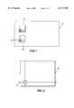
- FIG. 1is a top plan view of a memory device including a plurality of memory arrays.
- FIG. 2is a top plan view of a portion of one of the memory arrays of FIG. 1, including a memory cell manufactured in accordance with the present invention.
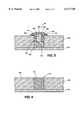
- FIG. 3is an elevation view of a cross-sectional cut along line 3--3 of the memory cell shown in FIG. 2, the memory cell having an electrode manufactured in accordance with the present invention
- FIG. 4is an elevation view of a cross-sectional cut of the electrode of FIG. 3 at an initial stage during the manufacturing process.
- FIG. 5is an elevation view of a cross-sectional cut of the electrode of FIG. 3 at an intermediate stage during the manufacturing process.
- FIG. 6is an elevation view of a cross-sectional cut of the electrode of FIG. 3 at a later intermediate stage during the manufacturing process.
- FIG. 7is an elevation view of a cross-sectional cut of the completed electrode of FIG. 3.
- FIG. 8is an elevation view of a cross-sectional cut of an alternative memory cell manufactured in accordance with the present invention.
- Memory devicesare integrated circuit (IC) devices that include built-in memory storage.
- a memory device 10 including a plurality of memory arrays 12is illustrated in FIG. 1.
- each memory array 12also called a memory core
- each memory array 12includes a plurality of memory cells 14 arranged to share connections in generally perpendicular rows (word lines) and columns (bit lines).
- Each memory cell 14can be accessed for reading or writing by a corresponding access or isolation device, generally placed within a base layer (not shown), by selecting the corresponding row and column coordinates.
- FIG. 3illustrates a memory cell 14 of the memory array 12 of the memory device 10.
- Memory cell 14includes a memory element 20, a conductive layer 30, and an electrode 40.
- the electrode 40is placed within a dielectric volume 50, which in turn is placed over a conductive plate 60.
- the conductive plate 60can be replaced by an active device, such as an access diode or a portion thereof.
- a layer 22 of a selected memory-storage materialis placed over the electrode 40.
- the area of the memory-storage material layer 22 proximally in contact with the electrode 40becomes an active area, the non-volatile resistive memory element 20.
- the conductive layer 30covers the memory-storage material layer 22.
- the memory-storage material layer 22 and the memory element 20include multi-state materials, such as chalcogenide.
- Suitable materials for the conductive layer 30include tungsten, titanium nitride, carbon, and molybdenum.
- the conductive layer 30can include a diffusion barrier and/or one or more conductive layers.
- the dielectric volume 50includes boron and phosphorus doped silicon dioxide glass (BPSG) or an inter-layer dielectric (ILD) such as plasma enhanced chemical vapor deposited silicon dioxide.
- the conductive plate 60can include, for example, polysilicon, single crystal silicon, and/or metal.
- the electrode 40rests within an opening 52 in the dielectric volume 50.
- the electrode 40includes a base portion 42, located at a lower cavity portion 53 of opening 52 and in direct contact with the conductive plate 60, a cylindrically shaped spacer 44, located along the sidewalls of an upper cavity portion 54 of opening 52, and a contact portion 46, placed inside of a central hole 55 in the spacer 44.
- the opening 52preferably has a depth-to-width ratio of at least 2:1.
- both the base portion 42 and the contact portion 46comprise tungsten or other materials that can be deposited using chemical vapor deposition (CVD).
- the spacer 44may be formed, for example, of silicon dioxide or silicon nitride.
- the depth-to-width ratio of both the opening 52 and the contact electrode 46is at least 2:1, and is preferably between 3:1 to 5:1.
- the lateral cross-sectional area of the contact portion 46is preferably less than 50% of the lateral cross-sectional area of the opening 52.
- the opening 52has a depth of 1.2 to 1.5 micrometers and a width/diameter of 0.4 to 0.5 micrometer.
- the contact portion 46has a depth of 0.3 micrometer and a width/diameter of 0.1 micrometers or less.
- the electrode 40 of FIG. 3is manufactured by a novel "plug-in-plug" process that allows the contact portion 46 of the electrode 40 to be much smaller than previous electrodes.
- a plug opening 52is first etched into the dielectric volume 50.
- the opening 52is then filled with a plug 61 of a chemical vapor deposited conductive material. Any excess material above a top surface 56 of dielectric volume 50 is removed by a dry chemical etch, a mechanical planarization, a chemical-mechanical planarization (CMP), or other comparable methods selected in reference to the particular materials utilized to form electrode 40.
- FIG. 4depicts the electrode 40 at the manufacturing stage after the plug 61 has been placed in opening 52 and planarized. The plug 61 is flush with top surface 56.
- the plug 61is recessed below the top surface 56 to form the base portion 42 and to leave free the upper cavity portion 54 of opening 52. This can be accomplished by over-etching during the excess-material removal dry chemical etch, or by another, subsequent etch process.
- the spacer 44can then be created by depositing and anisotropically etching an insulator/dielectric layer 43.
- This insulator/dielectric layercould be, for example, silicon oxide, silicon nitride or undoped silicon.
- FIG. 5illustrates the step of manufacture of the electrode 40 after the insulator layer 43 has been deposited, but before it has been etched.
- the spacer 44does not completely fill the upper cavity portion 54, leaving the central hole (or pore) 55 all the way down to the base portion 42.
- the spacer 44may have a flare 48 as a result of practical limitations upon by the deposition and etching process. As will be appreciated by those skilled in the art, the dimensions of spacer 44 will be determined substantially by the thickness of insulator/dielectric layer 43 deposition and by the degree of anisotropy achieved in the etch process.
- the contact electrode portion 46is created by depositing a layer 45 over the dielectric volume and filling the central hole 55.
- This layerwill typically be formed such as by using CVD or sputtering.
- layer 45will be a memory-storage material, such as a chalcogenide.
- the contact portion 46can act as the memory element without the need for an additional layer of memory-storage material.
- layer 45may simply be a conductive material, such as tungsten, carbon, etc., forming electrode 46.
- FIG. 7illustrates the finished electrode 40, the same as the one depicted in memory cell 14 of FIG. 3, after planarization.
- the contact portion 46is significantly reduced in size from that of the original plug 61 shown in FIG. 4.
- another layer 62may be formed above a plurality of electrodes 46.
- electrode 46is formed of a chalcogenide element
- layer 62may be an electrode assembly (which may include a diffusion barrier layer to protect the chalcogenide).
- layer 62may be a chalcogenide layer accessible by electrode 46.
- the planarizationcan be done to a point below top surface 56 (either by removing a top portion of fill material 45 or by removing both a top portion of fill material 45 and of the dielectric volume 50) so as to remove the flare 48 of spacer 44, so as to establish minimum hole/pore size.
- the contact portion 46is electrically coupled to the conductive plate 60 by the base portion 42.
Landscapes
- Engineering & Computer Science (AREA)
- Manufacturing & Machinery (AREA)
- Physics & Mathematics (AREA)
- Condensed Matter Physics & Semiconductors (AREA)
- General Physics & Mathematics (AREA)
- Computer Hardware Design (AREA)
- Microelectronics & Electronic Packaging (AREA)
- Power Engineering (AREA)
- Semiconductor Memories (AREA)
Abstract
Description
This application is a Divisional of application Ser. No. 08/486,635 filed Jun. 7, 1995.
The present invention relates generally to the use of electrodes in semiconductor devices, and more particularly relates to the formation of small electrodes having reduced contact areas which may be utilized, for example, in semiconductor memory devices. More specifically, the present invention relates to the manufacture of a small-sized electrode such as is useful to control the size of the active area of a chalcogenide resistive element in a memory cell of a chalcogenide memory device.
Electrodes are used in a variety of integrated circuit devices. In certain devices, such as memory devices, the ability to efficiently manufacture small electrodes is crucial in maximizing the performance and cost-efficiency of the device. A memory device can have a plurality of memory arrays, and each memory array can include hundreds of thousands of memory cells. Each memory cell generally includes a memory element and an access device (such as, for example, a diode) coupled to the memory element. Memory-storage materials, that is, materials that can be made to store information, such as by storing a charge or by changing resistivity, are used to fabricate the memory elements. Electrodes couple each memory element to a corresponding access device. The electrodes can be part of the access device and can also define the memory element.
In certain memory devices, such as memory devices having chalcogenide memory elements, the size of the electrode has a direct relationship to the speed, power requirements, and capacity of the memory device. Chalcogenides are materials which may be electrically stimulated to change states, from an amorphous state to a crystalline state, for example, or to exhibit different resistivities while in the crystalline state. Thus, chalcogenide memory elements can be utilized in memory devices for the storage of binary data, or of data represented in higher-based systems. Such memory cells will typically include a cell accessible, for example, by a potential applied to access lines, in a manner conventionally utilized in memory devices. Typically, the cell will include the chalcogenide element as a resistive element, and will include an access or isolation device coupled to the chalcogenide element. In one exemplary implementation suitable for use in a RAM, the access device may be a diode.
Many chalcogenide alloys may be contemplated for use with the present invention. For example, alloys of tellurium, antimony and germanium may be particularly desirable, and alloys having from approximately to 55-85 percent tellurium and on the order of 15-25 percent germanium are contemplated for use in accordance with the present invention. Preferably, the chalcogenide element will be generally homogeneous (although gradiented alloys may be utilized), and will be alloys formed from tellurium, selenium, germanium, antimony, bismuth, lead, strontium, arsenic, sulfur, silicon, phosphorus, oxygen and mixtures or alloys of such elements. The alloys will be selected so as to establish a material capable of assuming multiple, generally stable, states in response to a stimulus. It is contemplated that in most cases, the stimulus will represent an electrical signal, and that the multiple states will be states of differing electrical resistance. U.S. Pat. No. 5,335,219 is believed to be generally illustrative of the existing state of the art relative to chalcogenide materials, and is believed to provide explanations regarding the current theory of function and operation of chalcogenide elements and their use in memory cells. The specification of U.S. Pat. No. 5,335,219 to Ovshinski et al., issued Aug. 2, 1994, is incorporated herein by reference, for all purposes. An exemplary specific chalcogenide alloy suitable for use in the present invention is one consisting of Te56 Ge22 Sb22.
An observed property of a chalcogenide element in a memory cell is that the chalcogenide element will have an "active area" which may be less than the area of the entire chalcogenide element. The size of this active area can be controlled by controlling the size of the electrode contact with the chalcogenide element. A primary reason for limiting the active area of the chalcogenide element is that the size of the active area is directly related to the programming current and/or time required to achieve the desired state change. Thus, in the interest of optimally fast programming rates of a memory device, it is desirable to minimize the dimension of electrode contacting the chalcogenide element, to minimize the active area and to thereby facilitate optimally fast programming time and optimally low programming current.
Techniques for forming the electrode of a chalcogenide memory cell include forming a hole in a dielectric layer, and then depositing a conductive material in the hole. Conventional techniques of forming the hole in the insulative layer have included the application of a high current pulse to open a hole having a diameter of on the order of 0.1-0.2 microns. Additional attempts have been made to rely upon photolithography or etching to establish an opening through the insulative layer. All of these methods suffer from technological constraints upon the hole size, and offer less than optimal repeatability.
Accordingly, the present invention provides a new method and apparatus for creating small electrodes, so as, for example, to establish minimally-sized active areas in a chalcogenide layer disposed adjacent to such insulative layer. In a preferred implementation of the invention, the active area of the chalcogenide element can be generally controlled through selection of the electrode size in the insulative layer.
The present invention comprises an electrode suitable for use in a multi-state memory cell for use in a memory array of a memory device. The electrode includes a base portion and an upper portion. The base portion includes a recessed plug of conductive material configured for electrically coupling to an access device or to an access line. The upper portion includes a cylindrically shaped spacer of an insulative material, the spacer having a center hole, and a contact plug of conductive material, the contact plug placed inside the center hole. The contact plug electrically couples to the base portion and is configured for coupling to a multi-state element.
The electrode can be manufactured by first providing a dielectric volume and then etching an opening within the dielectric volume. The recessed plug of conductive material is then formed within a lower portion of the opening, preferably by chemical vapor deposition (CVD). The spacer is formed, generally by deposition and anisotropic etching, along the sidewalls of an upper portion of the opening. Finally the contact plug is formed within the central hole, preferably by CVD.
FIG. 1 is a top plan view of a memory device including a plurality of memory arrays.
FIG. 2 is a top plan view of a portion of one of the memory arrays of FIG. 1, including a memory cell manufactured in accordance with the present invention.
FIG. 3 is an elevation view of a cross-sectional cut alongline 3--3 of the memory cell shown in FIG. 2, the memory cell having an electrode manufactured in accordance with the present invention
FIG. 4 is an elevation view of a cross-sectional cut of the electrode of FIG. 3 at an initial stage during the manufacturing process.
FIG. 5 is an elevation view of a cross-sectional cut of the electrode of FIG. 3 at an intermediate stage during the manufacturing process.
FIG. 6 is an elevation view of a cross-sectional cut of the electrode of FIG. 3 at a later intermediate stage during the manufacturing process.
FIG. 7 is an elevation view of a cross-sectional cut of the completed electrode of FIG. 3.
FIG. 8 is an elevation view of a cross-sectional cut of an alternative memory cell manufactured in accordance with the present invention.
Memory devices are integrated circuit (IC) devices that include built-in memory storage. Amemory device 10 including a plurality ofmemory arrays 12 is illustrated in FIG. 1. As better seen in FIG. 2, each memory array 12 (also called a memory core) includes a plurality ofmemory cells 14 arranged to share connections in generally perpendicular rows (word lines) and columns (bit lines). Eachmemory cell 14 can be accessed for reading or writing by a corresponding access or isolation device, generally placed within a base layer (not shown), by selecting the corresponding row and column coordinates.
FIG. 3 illustrates amemory cell 14 of thememory array 12 of thememory device 10.Memory cell 14 includes amemory element 20, aconductive layer 30, and anelectrode 40. Theelectrode 40 is placed within adielectric volume 50, which in turn is placed over aconductive plate 60. In other embodiments, theconductive plate 60 can be replaced by an active device, such as an access diode or a portion thereof. Alayer 22 of a selected memory-storage material is placed over theelectrode 40. The area of the memory-storage material layer 22 proximally in contact with theelectrode 40 becomes an active area, the non-volatileresistive memory element 20. Theconductive layer 30 covers the memory-storage material layer 22.
In a preferred embodiment the memory-storage material layer 22 and thememory element 20 include multi-state materials, such as chalcogenide.
Suitable materials for theconductive layer 30 include tungsten, titanium nitride, carbon, and molybdenum. Theconductive layer 30 can include a diffusion barrier and/or one or more conductive layers. Thedielectric volume 50 includes boron and phosphorus doped silicon dioxide glass (BPSG) or an inter-layer dielectric (ILD) such as plasma enhanced chemical vapor deposited silicon dioxide. Theconductive plate 60 can include, for example, polysilicon, single crystal silicon, and/or metal.
Theelectrode 40 rests within anopening 52 in thedielectric volume 50. Theelectrode 40 includes abase portion 42, located at alower cavity portion 53 ofopening 52 and in direct contact with theconductive plate 60, a cylindrically shapedspacer 44, located along the sidewalls of anupper cavity portion 54 ofopening 52, and acontact portion 46, placed inside of acentral hole 55 in thespacer 44. Theopening 52 preferably has a depth-to-width ratio of at least 2:1.
In a preferred embodiment, both thebase portion 42 and thecontact portion 46 comprise tungsten or other materials that can be deposited using chemical vapor deposition (CVD). Thespacer 44 may be formed, for example, of silicon dioxide or silicon nitride. The depth-to-width ratio of both theopening 52 and thecontact electrode 46 is at least 2:1, and is preferably between 3:1 to 5:1. The lateral cross-sectional area of thecontact portion 46 is preferably less than 50% of the lateral cross-sectional area of theopening 52. In one exemplary embodiment, theopening 52 has a depth of 1.2 to 1.5 micrometers and a width/diameter of 0.4 to 0.5 micrometer. Thecontact portion 46 has a depth of 0.3 micrometer and a width/diameter of 0.1 micrometers or less.
Theelectrode 40 of FIG. 3 is manufactured by a novel "plug-in-plug" process that allows thecontact portion 46 of theelectrode 40 to be much smaller than previous electrodes. To manufactureelectrode 40, aplug opening 52 is first etched into thedielectric volume 50. Theopening 52 is then filled with aplug 61 of a chemical vapor deposited conductive material. Any excess material above atop surface 56 ofdielectric volume 50 is removed by a dry chemical etch, a mechanical planarization, a chemical-mechanical planarization (CMP), or other comparable methods selected in reference to the particular materials utilized to formelectrode 40. FIG. 4 depicts theelectrode 40 at the manufacturing stage after theplug 61 has been placed in opening 52 and planarized. Theplug 61 is flush withtop surface 56.
Next, theplug 61 is recessed below thetop surface 56 to form thebase portion 42 and to leave free theupper cavity portion 54 ofopening 52. This can be accomplished by over-etching during the excess-material removal dry chemical etch, or by another, subsequent etch process. Thespacer 44 can then be created by depositing and anisotropically etching an insulator/dielectric layer 43. This insulator/dielectric layer could be, for example, silicon oxide, silicon nitride or undoped silicon.
FIG. 5 illustrates the step of manufacture of theelectrode 40 after theinsulator layer 43 has been deposited, but before it has been etched. Thespacer 44 does not completely fill theupper cavity portion 54, leaving the central hole (or pore) 55 all the way down to thebase portion 42. Thespacer 44 may have aflare 48 as a result of practical limitations upon by the deposition and etching process. As will be appreciated by those skilled in the art, the dimensions ofspacer 44 will be determined substantially by the thickness of insulator/dielectric layer 43 deposition and by the degree of anisotropy achieved in the etch process.
Thecontact electrode portion 46 is created by depositing alayer 45 over the dielectric volume and filling thecentral hole 55. This layer will typically be formed such as by using CVD or sputtering. In a particularly preferred implementation,layer 45 will be a memory-storage material, such as a chalcogenide. In such an implementation, thecontact portion 46 can act as the memory element without the need for an additional layer of memory-storage material. Alternatively,layer 45 may simply be a conductive material, such as tungsten, carbon, etc., formingelectrode 46.
Excess material forming layer 45 (i.e., that material above the top surface 56) is removed using a dry chemical etch, a mechanical planarization, a chemical-mechanical planarization (CMP), or other methods that accomplish similar results. FIG. 7 illustrates thefinished electrode 40, the same as the one depicted inmemory cell 14 of FIG. 3, after planarization. Thecontact portion 46 is significantly reduced in size from that of theoriginal plug 61 shown in FIG. 4. As depicted in FIG. 8, anotherlayer 62 may be formed above a plurality ofelectrodes 46. Whereelectrode 46 is formed of a chalcogenide element,layer 62 may be an electrode assembly (which may include a diffusion barrier layer to protect the chalcogenide). Alternatively, whereelectrode 46 is merely a conductive plug,layer 62 may be a chalcogenide layer accessible byelectrode 46.
To further reduce the diameter of thecontact electrode 46, the planarization can be done to a point below top surface 56 (either by removing a top portion offill material 45 or by removing both a top portion offill material 45 and of the dielectric volume 50) so as to remove theflare 48 ofspacer 44, so as to establish minimum hole/pore size. Thecontact portion 46 is electrically coupled to theconductive plate 60 by thebase portion 42.
Accordingly, it should be readily understood that the embodiment described and illustrated herein are illustrative only, and are not be considered as limitations upon the scope of the present invention. Other variations and modifications may be made in accordance with the spirit and scope of the present invention.
Claims (18)
1. A method for manufacturing an electrode assembly, the method comprising the steps of:
forming a dielectric volume;
forming a plug opening within said dielectric volume;
forming a recessed plug of a conductive material within said plug opening;
forming a spacer within said plug opening to define a contact opening; and
forming a contact member of a memory material within said contact opening, said contact member electrically coupled to said recessed plug.
2. The method of claim 1, wherein said step of forming a plug opening within said dielectric volume includes etching an opening having a depth-to-width ratio of at least 2:1.
3. The method of claim 1, wherein said step of forming a spacer includes the steps of:
depositing a generally conformal insulative layer over said plug opening; and
anisotropically etching said insulative layer to form said spacer and said contact opening, said contact opening having a depth-to-width ratio of at least 2:1.
4. The method of claim 1, wherein said memory material comprises chalcogenide material.
5. A method for manufacturing a memory cell, the method comprising the steps of:
providing a dielectric volume;
forming a plug opening within said dielectric volume, said plug opening defined in part by sidewalls;
forming a recessed plug of a conductive material within a lower portion of said opening, the recessed plug configured for coupling to an access device;
forming a spacer along said sidewalls of said opening, said spacer defining an aperture;
forming a contact member within said aperture, said contact member electrically coupled to said recessed plug; and
disposing a memory-storage material over said contact member.
6. The method of claim 5, further comprising the step of disposing a conductive layer over said memory storage material.
7. The method of claim 5, wherein said step of disposing a memory-storage material comprises disposing a chalcogenide material.
8. The method of claim 1, wherein the memory material has a resistivity, the resistivity being variable in response to an electrical stimulus applied to the contact member.
9. The method of claim 1, wherein the memory material is changeable between a first physical state and a second physical state in response to an electrical stimulus applied to the contact member.
10. The method of claim 9, herein the first physical state comprises a generally amorphous state and the second physical state comprises a generally crystalline state.
11. The method of claim 5, wherein the memory-storage material has a resistivity, the resistivity being variable in response to an electrical stimulus applied to the memory-storage material.
12. The method of claim 5, wherein the memory material is changeable between a first physical state and a second physical state in response to an electrical stimulus applied to the memory-storage material.
13. The method of claim 12, wherein the first physical state comprises a generally amorphous state and the second physical state comprises a generally crystalline state.
14. A method for manufacturing a memory cell, the method comprising:
providing a dielectric member;
forming a first aperture in the dielectric member, said first aperture having a first portion and a second portion;
disposing a first conductive member within the first portion of the first aperture;
forming a dielectric spacer within the second portion of the first aperture to define a second aperture within the second portion of the first aperture; and
disposing a memory material within the second aperture, the memory material being electrically coupled to the first conductive member.
15. The method of claim 14, further comprising disposing a second conductive member on the memory material, the second conductive member being electrically coupled to the memory material.
16. The method of claim 14, wherein disposing the memory material comprises disposing a chalcogenide material within the second aperture.
17. The method of claim 14, wherein disposing the memory material comprises disposing a material having an electrically-sensitive resistivity within the second aperture.
18. The method of claim 14, wherein disposing the memory material comprises disposing a material changeable between a first physical state and a second physical state in response to an electrical stimulus.
Priority Applications (1)
| Application Number | Priority Date | Filing Date | Title |
|---|---|---|---|
| US08/847,824US6117720A (en) | 1995-06-07 | 1997-04-28 | Method of making an integrated circuit electrode having a reduced contact area |
Applications Claiming Priority (2)
| Application Number | Priority Date | Filing Date | Title |
|---|---|---|---|
| US08/486,635US6420725B1 (en) | 1995-06-07 | 1995-06-07 | Method and apparatus for forming an integrated circuit electrode having a reduced contact area |
| US08/847,824US6117720A (en) | 1995-06-07 | 1997-04-28 | Method of making an integrated circuit electrode having a reduced contact area |
Related Parent Applications (1)
| Application Number | Title | Priority Date | Filing Date |
|---|---|---|---|
| US08/486,635DivisionUS6420725B1 (en) | 1995-06-07 | 1995-06-07 | Method and apparatus for forming an integrated circuit electrode having a reduced contact area |
Publications (1)
| Publication Number | Publication Date |
|---|---|
| US6117720Atrue US6117720A (en) | 2000-09-12 |
Family
ID=23932658
Family Applications (6)
| Application Number | Title | Priority Date | Filing Date |
|---|---|---|---|
| US08/486,635Expired - LifetimeUS6420725B1 (en) | 1995-06-07 | 1995-06-07 | Method and apparatus for forming an integrated circuit electrode having a reduced contact area |
| US08/847,824Expired - LifetimeUS6117720A (en) | 1995-06-07 | 1997-04-28 | Method of making an integrated circuit electrode having a reduced contact area |
| US10/158,504Expired - Fee RelatedUS6831330B2 (en) | 1995-06-07 | 2002-05-30 | Method and apparatus for forming an integrated circuit electrode having a reduced contact area |
| US10/930,305Expired - Fee RelatedUS7271440B2 (en) | 1995-06-07 | 2004-08-31 | Method and apparatus for forming an integrated circuit electrode having a reduced contact area |
| US11/901,621Expired - Fee RelatedUS7687796B2 (en) | 1995-06-07 | 2007-09-18 | Method and apparatus for forming an integrated circuit electrode having a reduced contact area |
| US12/748,836Expired - Fee RelatedUS8017453B2 (en) | 1995-06-07 | 2010-03-29 | Method and apparatus for forming an integrated circuit electrode having a reduced contact area |
Family Applications Before (1)
| Application Number | Title | Priority Date | Filing Date |
|---|---|---|---|
| US08/486,635Expired - LifetimeUS6420725B1 (en) | 1995-06-07 | 1995-06-07 | Method and apparatus for forming an integrated circuit electrode having a reduced contact area |
Family Applications After (4)
| Application Number | Title | Priority Date | Filing Date |
|---|---|---|---|
| US10/158,504Expired - Fee RelatedUS6831330B2 (en) | 1995-06-07 | 2002-05-30 | Method and apparatus for forming an integrated circuit electrode having a reduced contact area |
| US10/930,305Expired - Fee RelatedUS7271440B2 (en) | 1995-06-07 | 2004-08-31 | Method and apparatus for forming an integrated circuit electrode having a reduced contact area |
| US11/901,621Expired - Fee RelatedUS7687796B2 (en) | 1995-06-07 | 2007-09-18 | Method and apparatus for forming an integrated circuit electrode having a reduced contact area |
| US12/748,836Expired - Fee RelatedUS8017453B2 (en) | 1995-06-07 | 2010-03-29 | Method and apparatus for forming an integrated circuit electrode having a reduced contact area |
Country Status (1)
| Country | Link |
|---|---|
| US (6) | US6420725B1 (en) |
Cited By (270)
| Publication number | Priority date | Publication date | Assignee | Title |
|---|---|---|---|---|
| WO2002027768A3 (en)* | 2000-09-27 | 2002-08-22 | Nuep2 Inc | Fabrication of semiconductor devices |
| US20020179896A1 (en)* | 1995-06-07 | 2002-12-05 | Harshfield Steven T. | Method and apparatus for forming an integrated circuit electrode having a reduced contact area |
| US20030045054A1 (en)* | 2001-08-29 | 2003-03-06 | Campbell Kristy A. | Method of forming non-volatile resistance variable devices, method of forming a programmable memory cell of memory circuitry, and a non-volatile resistance variable device |
| US6531391B2 (en) | 1996-07-22 | 2003-03-11 | Micron Technology, Inc. | Method of fabricating a conductive path in a semiconductor device |
| US6534368B2 (en) | 1997-01-28 | 2003-03-18 | Micron Technology, Inc. | Integrated circuit memory cell having a small active area and method of forming same |
| US20030068861A1 (en)* | 2001-08-30 | 2003-04-10 | Jiutao Li | Integrated circuit device and fabrication using metal-doped chalcogenide materials |
| US20030071289A1 (en)* | 2001-08-31 | 2003-04-17 | Hudgens Stephen J. | Multiple layer phase-change memory |
| US20030095426A1 (en)* | 2001-11-20 | 2003-05-22 | Glen Hush | Complementary bit PCRAM sense amplifier and method of operation |
| US6579760B1 (en) | 2002-03-28 | 2003-06-17 | Macronix International Co., Ltd. | Self-aligned, programmable phase change memory |
| US20030116794A1 (en)* | 2001-08-31 | 2003-06-26 | Lowrey Tyler A. | Elevated pore phase-change memory |
| US20030185036A1 (en)* | 2002-03-28 | 2003-10-02 | Micron Technology, Inc. | Method for programming a memory cell |
| US6638820B2 (en) | 2001-02-08 | 2003-10-28 | Micron Technology, Inc. | Method of forming chalcogenide comprising devices, method of precluding diffusion of a metal into adjacent chalcogenide material, and chalcogenide comprising devices |
| US20030206433A1 (en)* | 2002-05-03 | 2003-11-06 | Glen Hush | Dual write cycle programmable conductor memory system and method of operation |
| US6646902B2 (en) | 2001-08-30 | 2003-11-11 | Micron Technology, Inc. | Method of retaining memory state in a programmable conductor RAM |
| US6653193B2 (en) | 2000-12-08 | 2003-11-25 | Micron Technology, Inc. | Resistance variable device |
| WO2003065456A3 (en)* | 2002-01-31 | 2003-12-04 | Micron Technology Inc | Methods of forming non-volatile resistance variable devices and methods of forming silver selenide comprising structures |
| US20030228717A1 (en)* | 2002-06-06 | 2003-12-11 | Jiutao Li | Co-sputter deposition of metal-doped chalcogenides |
| US20040038432A1 (en)* | 2002-04-10 | 2004-02-26 | Micron Technology, Inc. | Programmable conductor memory cell structure and method therefor |
| US20040042259A1 (en)* | 2002-08-29 | 2004-03-04 | Campbell Kristy A. | Single polarity programming of a pcram structure |
| US20040043137A1 (en)* | 2002-08-09 | 2004-03-04 | Macronix International Co., Ltd. | Spacer chalcogenide memory method and device |
| WO2003023875A3 (en)* | 2001-09-07 | 2004-03-18 | Intel Corp | Phase change material memory device |
| US6710423B2 (en) | 2001-03-01 | 2004-03-23 | Micron Technology, Inc. | Chalcogenide comprising device |
| US20040085833A1 (en)* | 2002-11-01 | 2004-05-06 | Young-Nam Hwang | Phase changeable memory devices and methods of forming the same in which an upper electrode includes a tip that extends toward a lower electrode |
| US6734455B2 (en) | 2001-03-15 | 2004-05-11 | Micron Technology, Inc. | Agglomeration elimination for metal sputter deposition of chalcogenides |
| US6737312B2 (en) | 2001-08-27 | 2004-05-18 | Micron Technology, Inc. | Method of fabricating dual PCRAM cells sharing a common electrode |
| US20040124503A1 (en)* | 2000-07-14 | 2004-07-01 | Harshfield Steven T. | Memory elements and methods for making same |
| US6784018B2 (en) | 2001-08-29 | 2004-08-31 | Micron Technology, Inc. | Method of forming chalcogenide comprising devices and method of forming a programmable memory cell of memory circuitry |
| US6791885B2 (en) | 2002-02-19 | 2004-09-14 | Micron Technology, Inc. | Programmable conductor random access memory and method for sensing same |
| US20040179390A1 (en)* | 2003-03-12 | 2004-09-16 | Campbell Kristy A. | Chalcogenide glass constant current device, and its method of fabrication and operation |
| US6809362B2 (en) | 2002-02-20 | 2004-10-26 | Micron Technology, Inc. | Multiple data state memory cell |
| US6815818B2 (en) | 2001-11-19 | 2004-11-09 | Micron Technology, Inc. | Electrode structure for use in an integrated circuit |
| US6818481B2 (en) | 2001-03-07 | 2004-11-16 | Micron Technology, Inc. | Method to manufacture a buried electrode PCRAM cell |
| US6825135B2 (en) | 2002-06-06 | 2004-11-30 | Micron Technology, Inc. | Elimination of dendrite formation during metal/chalcogenide glass deposition |
| US6831019B1 (en) | 2002-08-29 | 2004-12-14 | Micron Technology, Inc. | Plasma etching methods and methods of forming memory devices comprising a chalcogenide comprising layer received operably proximate conductive electrodes |
| US6847535B2 (en) | 2002-02-20 | 2005-01-25 | Micron Technology, Inc. | Removable programmable conductor memory card and associated read/write device and method of operation |
| US6849868B2 (en) | 2002-03-14 | 2005-02-01 | Micron Technology, Inc. | Methods and apparatus for resistance variable material cells |
| US20050029504A1 (en)* | 2003-08-04 | 2005-02-10 | Karpov Ilya V. | Reducing parasitic conductive paths in phase change memories |
| US6855975B2 (en) | 2002-04-10 | 2005-02-15 | Micron Technology, Inc. | Thin film diode integrated with chalcogenide memory cell |
| US6858482B2 (en) | 2002-04-10 | 2005-02-22 | Micron Technology, Inc. | Method of manufacture of programmable switching circuits and memory cells employing a glass layer |
| US20050042799A1 (en)* | 2001-06-30 | 2005-02-24 | Lowrey Tyler A. | Pore structure for programmable device |
| US6867064B2 (en) | 2002-02-15 | 2005-03-15 | Micron Technology, Inc. | Method to alter chalcogenide glass for improved switching characteristics |
| US6867114B2 (en) | 2002-08-29 | 2005-03-15 | Micron Technology Inc. | Methods to form a memory cell with metal-rich metal chalcogenide |
| US6873538B2 (en) | 2001-12-20 | 2005-03-29 | Micron Technology, Inc. | Programmable conductor random access memory and a method for writing thereto |
| US6882578B2 (en) | 2002-01-04 | 2005-04-19 | Micron Technology, Inc. | PCRAM rewrite prevention |
| US6891749B2 (en) | 2002-02-20 | 2005-05-10 | Micron Technology, Inc. | Resistance variable ‘on ’ memory |
| US6903361B2 (en) | 2003-09-17 | 2005-06-07 | Micron Technology, Inc. | Non-volatile memory structure |
| US6930909B2 (en) | 2003-06-25 | 2005-08-16 | Micron Technology, Inc. | Memory device and methods of controlling resistance variation and resistance profile drift |
| US20050185444A1 (en)* | 2004-02-25 | 2005-08-25 | Soo-Guil Yang | Phase-changeable memory device and method of manufacturing the same |
| US6937528B2 (en) | 2002-03-05 | 2005-08-30 | Micron Technology, Inc. | Variable resistance memory and method for sensing same |
| US20050215009A1 (en)* | 2004-03-19 | 2005-09-29 | Sung-Lae Cho | Methods of forming phase-change memory devices |
| US6951805B2 (en) | 2001-08-01 | 2005-10-04 | Micron Technology, Inc. | Method of forming integrated circuitry, method of forming memory circuitry, and method of forming random access memory circuitry |
| US20050227496A1 (en)* | 2004-04-10 | 2005-10-13 | Joon-Sang Park | Phase change memory elements and methods of fabricating phase change memory elements having a confined portion of phase change material on a recessed contact |
| US6955940B2 (en) | 2001-08-29 | 2005-10-18 | Micron Technology, Inc. | Method of forming chalcogenide comprising devices |
| US20060001065A1 (en)* | 2004-07-01 | 2006-01-05 | Jang-Eun Heo | Alignment key structures in semiconductor devices including protected electrode structures and methods of fabricating the same |
| US20060019497A1 (en)* | 2004-07-22 | 2006-01-26 | Zhizhang Chen | Reduced feature-size memory devices and methods for fabricating the same |
| US20060040485A1 (en)* | 2004-08-20 | 2006-02-23 | Lee Jang-Eun | Method of forming via structures and method of fabricating phase change memory devices incorporating such via structures |
| US7010644B2 (en) | 2002-08-29 | 2006-03-07 | Micron Technology, Inc. | Software refreshed memory device and method |
| US7015494B2 (en) | 2002-07-10 | 2006-03-21 | Micron Technology, Inc. | Assemblies displaying differential negative resistance |
| US7018863B2 (en) | 2002-08-22 | 2006-03-28 | Micron Technology, Inc. | Method of manufacture of a resistance variable memory cell |
| US7022579B2 (en) | 2003-03-14 | 2006-04-04 | Micron Technology, Inc. | Method for filling via with metal |
| US20060094236A1 (en)* | 2004-11-03 | 2006-05-04 | Elkins Patricia C | Electroless plating of metal caps for chalcogenide-based memory devices |
| US20060091476A1 (en)* | 2004-10-29 | 2006-05-04 | Cay-Uwe Pinnow | Sub-lithographic structures, devices including such structures, and methods for producing the same |
| US7049009B2 (en) | 2002-08-29 | 2006-05-23 | Micron Technology, Inc. | Silver selenide film stoichiometry and morphology control in sputter deposition |
| US7050327B2 (en) | 2003-04-10 | 2006-05-23 | Micron Technology, Inc. | Differential negative resistance memory |
| US7061004B2 (en) | 2003-07-21 | 2006-06-13 | Micron Technology, Inc. | Resistance variable memory elements and methods of formation |
| US20060124916A1 (en)* | 2004-12-09 | 2006-06-15 | Macronix International Co., Ltd. | Self-aligned small contact phase-change memory method and device |
| US7071021B2 (en) | 2001-05-11 | 2006-07-04 | Micron Technology, Inc. | PCRAM memory cell and method of making same |
| DE102005001902A1 (en)* | 2005-01-14 | 2006-07-27 | Infineon Technologies Ag | Sub-lithographic contact structure manufacture, for semiconductor device, involves etching resistance changing material in through holes and separating layer from electrically conducting material to form contact electrode |
| US7087919B2 (en) | 2002-02-20 | 2006-08-08 | Micron Technology, Inc. | Layered resistance variable memory device and method of fabrication |
| US7098068B2 (en) | 2004-03-10 | 2006-08-29 | Micron Technology, Inc. | Method of forming a chalcogenide material containing device |
| US7151273B2 (en) | 2002-02-20 | 2006-12-19 | Micron Technology, Inc. | Silver-selenide/chalcogenide glass stack for resistance variable memory |
| US7151688B2 (en) | 2004-09-01 | 2006-12-19 | Micron Technology, Inc. | Sensing of resistance variable memory devices |
| US20060284158A1 (en)* | 2005-06-17 | 2006-12-21 | Macronix International Co., Ltd. | Self-aligned, embedded phase change ram and manufacturing method |
| US20060284157A1 (en)* | 2005-06-17 | 2006-12-21 | Macronix International Co., Ltd. | Thin film plate phase change RAM circuit and manufacturing method |
| US20060286709A1 (en)* | 2005-06-17 | 2006-12-21 | Macronix International Co., Ltd. | Manufacturing methods for thin film fuse phase change ram |
| US20060284279A1 (en)* | 2005-06-17 | 2006-12-21 | Macronix International Co., Ltd. | Thin film fuse phase change RAM and manufacturing method |
| US20060284214A1 (en)* | 2005-06-17 | 2006-12-21 | Macronix International Co., Ltd. | Thin film fuse phase change cell with thermal isolation layer and manufacturing method |
| US20060286743A1 (en)* | 2005-06-17 | 2006-12-21 | Macronix International Co., Ltd. | Method for Manufacturing a Narrow Structure on an Integrated Circuit |
| US7163837B2 (en) | 2002-08-29 | 2007-01-16 | Micron Technology, Inc. | Method of forming a resistance variable memory element |
| US7190048B2 (en) | 2004-07-19 | 2007-03-13 | Micron Technology, Inc. | Resistance variable memory device and method of fabrication |
| DE10214702B4 (en)* | 2001-07-25 | 2007-03-29 | Promos Technologies, Inc. | Method for producing electrodes on a semiconductor substrate |
| US7209378B2 (en) | 2002-08-08 | 2007-04-24 | Micron Technology, Inc. | Columnar 1T-N memory cell structure |
| US20070111429A1 (en)* | 2005-11-14 | 2007-05-17 | Macronix International Co., Ltd. | Method of manufacturing a pipe shaped phase change memory |
| US20070109836A1 (en)* | 2005-11-15 | 2007-05-17 | Macronix International Co., Ltd. | Thermally insulated phase change memory device and manufacturing method |
| US20070109843A1 (en)* | 2005-11-15 | 2007-05-17 | Macronix International Co., Ltd. | Phase Change Memory Device and Manufacturing Method |
| US20070121363A1 (en)* | 2005-11-28 | 2007-05-31 | Macronix International Co., Ltd. | Phase Change Memory Cell and Manufacturing Method |
| US20070126045A1 (en)* | 2005-12-05 | 2007-06-07 | Sung-Yool Choi | Memory devices including dielectric thin film and method of manufacturing the same |
| US20070131980A1 (en)* | 2005-11-21 | 2007-06-14 | Lung Hsiang L | Vacuum jacket for phase change memory element |
| US20070131922A1 (en)* | 2005-12-13 | 2007-06-14 | Macronix International Co., Ltd. | Thin Film Fuse Phase Change Cell with Thermal Isolation Pad and Manufacturing Method |
| US7233520B2 (en) | 2005-07-08 | 2007-06-19 | Micron Technology, Inc. | Process for erasing chalcogenide variable resistance memory bits |
| US20070154847A1 (en)* | 2005-12-30 | 2007-07-05 | Macronix International Co., Ltd. | Chalcogenide layer etching method |
| US20070155172A1 (en)* | 2005-12-05 | 2007-07-05 | Macronix International Co., Ltd. | Manufacturing Method for Phase Change RAM with Electrode Layer Process |
| US20070158645A1 (en)* | 2006-01-11 | 2007-07-12 | Macronix International Co., Ltd. | Self-align planerized bottom electrode phase change memory and manufacturing method |
| US20070158690A1 (en)* | 2006-01-09 | 2007-07-12 | Macronix International Co., Ltd. | Programmable Resistive RAM and Manufacturing Method |
| US20070161186A1 (en)* | 2006-01-09 | 2007-07-12 | Macronix International Co., Ltd. | Programmable Resistive RAM and Manufacturing Method |
| US7251154B2 (en) | 2005-08-15 | 2007-07-31 | Micron Technology, Inc. | Method and apparatus providing a cross-point memory array using a variable resistance memory cell and capacitance |
| US20070176261A1 (en)* | 2006-01-30 | 2007-08-02 | Macronix International Co., Ltd. | Vertical Side Wall Active Pin Structures in a Phase Change Memory and Manufacturing Methods |
| DE10351017B4 (en)* | 2002-11-01 | 2007-09-06 | Samsung Electronics Co., Ltd., Suwon | Phase change memory cells and methods of making the same |
| US7269079B2 (en) | 2005-05-16 | 2007-09-11 | Micron Technology, Inc. | Power circuits for reducing a number of power supply voltage taps required for sensing a resistive memory |
| US7269044B2 (en) | 2005-04-22 | 2007-09-11 | Micron Technology, Inc. | Method and apparatus for accessing a memory array |
| US7274034B2 (en) | 2005-08-01 | 2007-09-25 | Micron Technology, Inc. | Resistance variable memory device with sputtered metal-chalcogenide region and method of fabrication |
| US7277313B2 (en) | 2005-08-31 | 2007-10-02 | Micron Technology, Inc. | Resistance variable memory element with threshold device and method of forming the same |
| US20070241371A1 (en)* | 2006-04-17 | 2007-10-18 | Macronix International Co., Ltd. | Memory device and manufacturing method |
| US20070246782A1 (en)* | 2006-04-19 | 2007-10-25 | Philipp Jan B | Memory cell having sidewall spacer for improved homogeneity |
| US20070257300A1 (en)* | 2006-05-05 | 2007-11-08 | Macronix International Co., Ltd. | Structures and Methods of a Bistable Resistive Random Access Memory |
| US7294527B2 (en) | 2002-08-29 | 2007-11-13 | Micron Technology Inc. | Method of forming a memory cell |
| US20070262388A1 (en)* | 2006-05-09 | 2007-11-15 | Macronix International Co., Ltd. | Bridge Resistance Random Access Memory Device and Method With A Singular Contact Structure |
| US7304368B2 (en) | 2005-08-11 | 2007-12-04 | Micron Technology, Inc. | Chalcogenide-based electrokinetic memory element and method of forming the same |
| US20070281420A1 (en)* | 2006-05-30 | 2007-12-06 | Macronix International Co., Ltd. | Resistor random access memory cell with reduced active area and reduced contact areas |
| US20070278529A1 (en)* | 2006-05-30 | 2007-12-06 | Macronix International Co., Ltd. | Resistor random access memory cell with l-shaped electrode |
| US7317567B2 (en) | 2005-08-02 | 2008-01-08 | Micron Technology, Inc. | Method and apparatus for providing color changing thin film material |
| US7317200B2 (en) | 2005-02-23 | 2008-01-08 | Micron Technology, Inc. | SnSe-based limited reprogrammable cell |
| US20080016414A1 (en)* | 2000-06-22 | 2008-01-17 | Contour Semiconductor, Inc. | Low Cost High Density Rectifier Matrix Memory |
| US20080011999A1 (en)* | 2003-12-12 | 2008-01-17 | Samsung Electronics Co., Ltd. | Microelectronic Devices Using Sacrificial Layers and Structures Fabricated by Same |
| US7326950B2 (en) | 2004-07-19 | 2008-02-05 | Micron Technology, Inc. | Memory device with switching glass layer |
| US7332735B2 (en) | 2005-08-02 | 2008-02-19 | Micron Technology, Inc. | Phase change memory cell and method of formation |
| US20080043520A1 (en)* | 2006-02-07 | 2008-02-21 | Chen Shih H | I-shaped phase change memory cell with thermal isolation |
| US7354793B2 (en) | 2004-08-12 | 2008-04-08 | Micron Technology, Inc. | Method of forming a PCRAM device incorporating a resistance-variable chalocogenide element |
| US20080096341A1 (en)* | 2006-10-24 | 2008-04-24 | Macronix International Co., Ltd. | Method for Manufacturing a Resistor Random Access Memory with Reduced Active Area and Reduced Contact Areas |
| US20080096375A1 (en)* | 2006-10-18 | 2008-04-24 | Macronix International Co., Ltd. | Method for Making Memory Cell Device |
| US20080094885A1 (en)* | 2006-10-24 | 2008-04-24 | Macronix International Co., Ltd. | Bistable Resistance Random Access Memory Structures with Multiple Memory Layers and Multilevel Memory States |
| US7365411B2 (en) | 2004-08-12 | 2008-04-29 | Micron Technology, Inc. | Resistance variable memory with temperature tolerant materials |
| US20080099791A1 (en)* | 2006-10-04 | 2008-05-01 | Macronix International Co., Ltd. | Memory Cell Device with Circumferentially-Extending Memory Element |
| US20080108174A1 (en)* | 2006-11-07 | 2008-05-08 | Samsung Electronics Co., Ltd. | Metal precursors for low temperature deposition and methods of forming a metal thin layer and manufacturing a phase-change memory device using the metal precursors |
| US7374174B2 (en) | 2004-12-22 | 2008-05-20 | Micron Technology, Inc. | Small electrode for resistance variable devices |
| US20080116443A1 (en)* | 2006-11-16 | 2008-05-22 | Heon Yong Chang | Phase change memory device with hole for a lower electrode defined in a stable manner and method for manufacturing the same |
| US20080116440A1 (en)* | 2006-11-16 | 2008-05-22 | Macronix International Co., Ltd. | Resistance Random Access Memory Structure for Enhanced Retention |
| US20080121861A1 (en)* | 2006-08-16 | 2008-05-29 | Macronix International Co., Ltd. | Self-Aligned Structure and Method for Confining a Melting Point in a Resistor Random Access Memory |
| US7385868B2 (en) | 2003-07-08 | 2008-06-10 | Micron Technology, Inc. | Method of refreshing a PCRAM memory device |
| US20080138931A1 (en)* | 2006-12-06 | 2008-06-12 | Macronix International Co., Ltd. | Method for Making a Self-Converged Void and Bottom Electrode for Memoery Cell |
| US20080138929A1 (en)* | 2006-12-06 | 2008-06-12 | Macronix International Co., Ltd. | Method for Making a Self-Converged Memory Material Element for Memory Cell |
| US20080135824A1 (en)* | 2006-12-07 | 2008-06-12 | Macronix International Co., Ltd. | Method and Structure of a Multi-Level Cell Resistance Random Access Memory with Metal Oxides |
| US7388771B2 (en) | 2006-10-24 | 2008-06-17 | Macronix International Co., Ltd. | Methods of operating a bistable resistance random access memory with multiple memory layers and multilevel memory states |
| US20080157053A1 (en)* | 2006-12-28 | 2008-07-03 | Macronix International Co., Ltd. | Resistor Random Access Memory Cell Device |
| US7397060B2 (en) | 2005-11-14 | 2008-07-08 | Macronix International Co., Ltd. | Pipe shaped phase change memory |
| US20080165570A1 (en)* | 2007-01-05 | 2008-07-10 | Macronix International Co., Ltd. | Current Compliant Sensing Architecture for Multilevel Phase Change Memory |
| US20080186761A1 (en)* | 2007-02-07 | 2008-08-07 | Macronix International Co., Ltd. | Memory Cell with Separate Read and Program Paths |
| US7414258B2 (en) | 2005-11-16 | 2008-08-19 | Macronix International Co., Ltd. | Spacer electrode small pin phase change memory RAM and manufacturing method |
| US20080197334A1 (en)* | 2007-02-21 | 2008-08-21 | Macronix International Co., Ltd. | Phase Change Memory Cell with Heater and Method for Fabricating the Same |
| US20080197333A1 (en)* | 2007-02-21 | 2008-08-21 | Macronix International Co., Ltd. | Programmable Resistive Memory Cell with Self-Forming Gap |
| US20080203375A1 (en)* | 2007-02-27 | 2008-08-28 | Macronix International Co., Ltd. | Memory Cell with Memory Element Contacting Ring-Shaped Upper End of Bottom Electrode |
| US7423300B2 (en) | 2006-05-24 | 2008-09-09 | Macronix International Co., Ltd. | Single-mask phase change memory element |
| US7427770B2 (en) | 2005-04-22 | 2008-09-23 | Micron Technology, Inc. | Memory array for increased bit density |
| US7432206B2 (en) | 2006-01-24 | 2008-10-07 | Macronix International Co., Ltd. | Self-aligned manufacturing method, and manufacturing method for thin film fuse phase change ram |
| US7433226B2 (en) | 2007-01-09 | 2008-10-07 | Macronix International Co., Ltd. | Method, apparatus and computer program product for read before programming process on multiple programmable resistive memory cell |
| US7440315B2 (en) | 2007-01-09 | 2008-10-21 | Macronix International Co., Ltd. | Method, apparatus and computer program product for stepped reset programming process on programmable resistive memory cell |
| US20080258126A1 (en)* | 2007-04-17 | 2008-10-23 | Macronix International Co., Ltd. | Memory Cell Sidewall Contacting Side Electrode |
| US20080266933A1 (en)* | 2007-04-24 | 2008-10-30 | Macronix International Co., Ltd. | Method and Apparatus for Refreshing Programmable Resistive Memory |
| US20080268568A1 (en)* | 2007-04-24 | 2008-10-30 | Micron Technology, Inc. | Material sidewall deposition method |
| US20080268569A1 (en)* | 2004-06-30 | 2008-10-30 | Heon Yong Chang | Phase-change memory device and method of manufacturing the same |
| US20080272358A1 (en)* | 2007-05-02 | 2008-11-06 | Industrial Technology Research Institute | Phase change memory devices and methods for fabricating the same |
| US7450411B2 (en) | 2005-11-15 | 2008-11-11 | Macronix International Co., Ltd. | Phase change memory device and manufacturing method |
| US20080278989A1 (en)* | 2007-05-11 | 2008-11-13 | Samsung Electronics Co., Ltd. | Resistive memory device and method of manufacturing the same |
| US7463512B2 (en) | 2007-02-08 | 2008-12-09 | Macronix International Co., Ltd. | Memory element with reduced-current phase change element |
| US7479649B2 (en) | 2005-11-21 | 2009-01-20 | Macronix International Co., Ltd. | Vacuum jacketed electrode for phase change memory element |
| US7507986B2 (en) | 2005-11-21 | 2009-03-24 | Macronix International Co., Ltd. | Thermal isolation for an active-sidewall phase change memory cell |
| US7521364B2 (en) | 2005-12-02 | 2009-04-21 | Macronix Internation Co., Ltd. | Surface topology improvement method for plug surface areas |
| US20090109726A1 (en)* | 2007-10-29 | 2009-04-30 | Shepard Daniel R | Non-linear conductor memory |
| US7531825B2 (en) | 2005-12-27 | 2009-05-12 | Macronix International Co., Ltd. | Method for forming self-aligned thermal isolation cell for a variable resistance memory array |
| US7535756B2 (en) | 2007-01-31 | 2009-05-19 | Macronix International Co., Ltd. | Method to tighten set distribution for PCRAM |
| US7534647B2 (en) | 2005-06-17 | 2009-05-19 | Macronix International Co., Ltd. | Damascene phase change RAM and manufacturing method |
| US7551473B2 (en) | 2007-10-12 | 2009-06-23 | Macronix International Co., Ltd. | Programmable resistive memory with diode structure |
| US7560337B2 (en) | 2006-01-09 | 2009-07-14 | Macronix International Co., Ltd. | Programmable resistive RAM and manufacturing method |
| US7579615B2 (en) | 2005-08-09 | 2009-08-25 | Micron Technology, Inc. | Access transistor for memory device |
| US7583551B2 (en) | 2004-03-10 | 2009-09-01 | Micron Technology, Inc. | Power management control and controlling memory refresh operations |
| US20090225621A1 (en)* | 2008-03-05 | 2009-09-10 | Shepard Daniel R | Split decoder storage array and methods of forming the same |
| US7599217B2 (en) | 2005-11-22 | 2009-10-06 | Macronix International Co., Ltd. | Memory cell device and manufacturing method |
| US7608503B2 (en) | 2004-11-22 | 2009-10-27 | Macronix International Co., Ltd. | Side wall active pin memory and manufacturing method |
| US7619311B2 (en) | 2007-02-02 | 2009-11-17 | Macronix International Co., Ltd. | Memory cell device with coplanar electrode surface and method |
| US20090296445A1 (en)* | 2008-06-02 | 2009-12-03 | Shepard Daniel R | Diode decoder array with non-sequential layout and methods of forming the same |
| US7635855B2 (en) | 2005-11-15 | 2009-12-22 | Macronix International Co., Ltd. | I-shaped phase change memory cell |
| US7639527B2 (en) | 2008-01-07 | 2009-12-29 | Macronix International Co., Ltd. | Phase change memory dynamic resistance test and manufacturing methods |
| US7642125B2 (en) | 2007-09-14 | 2010-01-05 | Macronix International Co., Ltd. | Phase change memory cell in via array with self-aligned, self-converged bottom electrode and method for manufacturing |
| US7646631B2 (en) | 2007-12-07 | 2010-01-12 | Macronix International Co., Ltd. | Phase change memory cell having interface structures with essentially equal thermal impedances and manufacturing methods |
| US7663135B2 (en) | 2007-01-31 | 2010-02-16 | Macronix International Co., Ltd. | Memory cell having a side electrode contact |
| US7663133B2 (en) | 2005-04-22 | 2010-02-16 | Micron Technology, Inc. | Memory elements having patterned electrodes and method of forming the same |
| US20100065803A1 (en)* | 2006-12-04 | 2010-03-18 | Electronics And Telecommunications Research Institute | Memory device and manufacturing method thereof |
| US7682868B2 (en) | 2006-12-06 | 2010-03-23 | Macronix International Co., Ltd. | Method for making a keyhole opening during the manufacture of a memory cell |
| US7688619B2 (en) | 2005-11-28 | 2010-03-30 | Macronix International Co., Ltd. | Phase change memory cell and manufacturing method |
| US7692177B2 (en) | 2002-08-29 | 2010-04-06 | Micron Technology, Inc. | Resistance variable memory element and its method of formation |
| US20100085830A1 (en)* | 2008-10-07 | 2010-04-08 | Shepard Daniel R | Sequencing Decoder Circuit |
| US7696506B2 (en) | 2006-06-27 | 2010-04-13 | Macronix International Co., Ltd. | Memory cell with memory material insulation and manufacturing method |
| US7696503B2 (en) | 2005-06-17 | 2010-04-13 | Macronix International Co., Ltd. | Multi-level memory cell having phase change element and asymmetrical thermal boundary |
| US7701759B2 (en) | 2007-02-05 | 2010-04-20 | Macronix International Co., Ltd. | Memory cell device and programming methods |
| US7701750B2 (en) | 2008-05-08 | 2010-04-20 | Macronix International Co., Ltd. | Phase change device having two or more substantial amorphous regions in high resistance state |
| US7719913B2 (en) | 2008-09-12 | 2010-05-18 | Macronix International Co., Ltd. | Sensing circuit for PCRAM applications |
| US7729161B2 (en) | 2007-08-02 | 2010-06-01 | Macronix International Co., Ltd. | Phase change memory with dual word lines and source lines and method of operating same |
| US7755076B2 (en) | 2007-04-17 | 2010-07-13 | Macronix International Co., Ltd. | 4F2 self align side wall active phase change memory |
| US20100177553A1 (en)* | 2009-01-14 | 2010-07-15 | Macronix International Co., Ltd. | Rewritable memory device |
| US7772581B2 (en) | 2006-09-11 | 2010-08-10 | Macronix International Co., Ltd. | Memory device having wide area phase change element and small electrode contact area |
| US7777215B2 (en) | 2007-07-20 | 2010-08-17 | Macronix International Co., Ltd. | Resistive memory structure with buffer layer |
| US7786461B2 (en) | 2007-04-03 | 2010-08-31 | Macronix International Co., Ltd. | Memory structure with reduced-size memory element between memory material portions |
| US7785920B2 (en) | 2006-07-12 | 2010-08-31 | Macronix International Co., Ltd. | Method for making a pillar-type phase change memory element |
| US7791058B2 (en) | 2006-08-29 | 2010-09-07 | Micron Technology, Inc. | Enhanced memory density resistance variable memory cells, arrays, devices and systems including the same, and methods of fabrication |
| US7791057B2 (en) | 2008-04-22 | 2010-09-07 | Macronix International Co., Ltd. | Memory cell having a buried phase change region and method for fabricating the same |
| USRE41733E1 (en) | 1996-03-05 | 2010-09-21 | Contour Semiconductor, Inc. | Dual-addressed rectifier storage device |
| US7804083B2 (en) | 2007-11-14 | 2010-09-28 | Macronix International Co., Ltd. | Phase change memory cell including a thermal protect bottom electrode and manufacturing methods |
| US7816661B2 (en) | 2005-11-21 | 2010-10-19 | Macronix International Co., Ltd. | Air cell thermal isolation for a memory array formed of a programmable resistive material |
| US7825398B2 (en) | 2008-04-07 | 2010-11-02 | Macronix International Co., Ltd. | Memory cell having improved mechanical stability |
| US7829876B2 (en) | 2005-11-21 | 2010-11-09 | Macronix International Co., Ltd. | Vacuum cell thermal isolation for a phase change memory device |
| US20100321987A1 (en)* | 2009-06-22 | 2010-12-23 | Macronix International Co., Ltd. | Memory device and method for sensing and fixing margin cells |
| US20100328996A1 (en)* | 2009-06-25 | 2010-12-30 | Macronix International Co., Ltd. | Phase change memory having one or more non-constant doping profiles |
| US20100328995A1 (en)* | 2009-06-25 | 2010-12-30 | Macronix International Co., Ltd. | Methods and apparatus for reducing defect bits in phase change memory |
| US7863655B2 (en) | 2006-10-24 | 2011-01-04 | Macronix International Co., Ltd. | Phase change memory cells with dual access devices |
| US7869270B2 (en) | 2008-12-29 | 2011-01-11 | Macronix International Co., Ltd. | Set algorithm for phase change memory cell |
| US20110012079A1 (en)* | 2009-07-15 | 2011-01-20 | Macronix International Co., Ltd. | Thermal protect pcram structure and methods for making |
| US20110013446A1 (en)* | 2009-07-15 | 2011-01-20 | Macronix International Co., Ltd. | Refresh circuitry for phase change memory |
| US20110012083A1 (en)* | 2009-07-15 | 2011-01-20 | Macronix International Co., Ltd. | Phase change memory cell structure |
| US7879643B2 (en) | 2008-01-18 | 2011-02-01 | Macronix International Co., Ltd. | Memory cell with memory element contacting an inverted T-shaped bottom electrode |
| US7879645B2 (en) | 2008-01-28 | 2011-02-01 | Macronix International Co., Ltd. | Fill-in etching free pore device |
| US7884343B2 (en) | 2007-02-14 | 2011-02-08 | Macronix International Co., Ltd. | Phase change memory cell with filled sidewall memory element and method for fabricating the same |
| US7884342B2 (en) | 2007-07-31 | 2011-02-08 | Macronix International Co., Ltd. | Phase change memory bridge cell |
| US7897954B2 (en) | 2008-10-10 | 2011-03-01 | Macronix International Co., Ltd. | Dielectric-sandwiched pillar memory device |
| US20110049456A1 (en)* | 2009-09-03 | 2011-03-03 | Macronix International Co., Ltd. | Phase change structure with composite doping for phase change memory |
| US7903447B2 (en) | 2006-12-13 | 2011-03-08 | Macronix International Co., Ltd. | Method, apparatus and computer program product for read before programming process on programmable resistive memory cell |
| US7903457B2 (en) | 2008-08-19 | 2011-03-08 | Macronix International Co., Ltd. | Multiple phase change materials in an integrated circuit for system on a chip application |
| US20110063902A1 (en)* | 2009-09-17 | 2011-03-17 | Macronix International Co., Ltd. | 2t2r-1t1r mix mode phase change memory array |
| US7910907B2 (en) | 2006-03-15 | 2011-03-22 | Macronix International Co., Ltd. | Manufacturing method for pipe-shaped electrode phase change memory |
| US7919766B2 (en) | 2007-10-22 | 2011-04-05 | Macronix International Co., Ltd. | Method for making self aligning pillar memory cell device |
| US7928421B2 (en) | 2006-04-21 | 2011-04-19 | Macronix International Co., Ltd. | Phase change memory cell with vacuum spacer |
| US7933139B2 (en) | 2009-05-15 | 2011-04-26 | Macronix International Co., Ltd. | One-transistor, one-resistor, one-capacitor phase change memory |
| US7932506B2 (en) | 2008-07-22 | 2011-04-26 | Macronix International Co., Ltd. | Fully self-aligned pore-type memory cell having diode access device |
| US20110097825A1 (en)* | 2009-10-23 | 2011-04-28 | Macronix International Co., Ltd. | Methods For Reducing Recrystallization Time for a Phase Change Material |
| US7968876B2 (en) | 2009-05-22 | 2011-06-28 | Macronix International Co., Ltd. | Phase change memory cell having vertical channel access transistor |
| US8030634B2 (en) | 2008-03-31 | 2011-10-04 | Macronix International Co., Ltd. | Memory array with diode driver and method for fabricating the same |
| US8030635B2 (en) | 2009-01-13 | 2011-10-04 | Macronix International Co., Ltd. | Polysilicon plug bipolar transistor for phase change memory |
| US8036014B2 (en) | 2008-11-06 | 2011-10-11 | Macronix International Co., Ltd. | Phase change memory program method without over-reset |
| US8077505B2 (en) | 2008-05-07 | 2011-12-13 | Macronix International Co., Ltd. | Bipolar switching of phase change device |
| US8084760B2 (en) | 2009-04-20 | 2011-12-27 | Macronix International Co., Ltd. | Ring-shaped electrode and manufacturing method for same |
| US8084842B2 (en) | 2008-03-25 | 2011-12-27 | Macronix International Co., Ltd. | Thermally stabilized electrode structure |
| US8089137B2 (en) | 2009-01-07 | 2012-01-03 | Macronix International Co., Ltd. | Integrated circuit memory with single crystal silicon on silicide driver and manufacturing method |
| US8097871B2 (en) | 2009-04-30 | 2012-01-17 | Macronix International Co., Ltd. | Low operational current phase change memory structures |
| US8107283B2 (en) | 2009-01-12 | 2012-01-31 | Macronix International Co., Ltd. | Method for setting PCRAM devices |
| US8134857B2 (en) | 2008-06-27 | 2012-03-13 | Macronix International Co., Ltd. | Methods for high speed reading operation of phase change memory and device employing same |
| US8138028B2 (en) | 2007-02-12 | 2012-03-20 | Macronix International Co., Ltd | Method for manufacturing a phase change memory device with pillar bottom electrode |
| US8158965B2 (en) | 2008-02-05 | 2012-04-17 | Macronix International Co., Ltd. | Heating center PCRAM structure and methods for making |
| US8173987B2 (en) | 2009-04-27 | 2012-05-08 | Macronix International Co., Ltd. | Integrated circuit 3D phase change memory array and manufacturing method |
| US8178386B2 (en) | 2007-09-14 | 2012-05-15 | Macronix International Co., Ltd. | Phase change memory cell array with self-converged bottom electrode and method for manufacturing |
| US8310864B2 (en) | 2010-06-15 | 2012-11-13 | Macronix International Co., Ltd. | Self-aligned bit line under word line memory array |
| US8324605B2 (en) | 2008-10-02 | 2012-12-04 | Macronix International Co., Ltd. | Dielectric mesh isolated phase change structure for phase change memory |
| US8324681B2 (en) | 2005-12-09 | 2012-12-04 | Macronix International Co., Ltd. | Stacked non-volatile memory device and methods for fabricating the same |
| US8344347B2 (en) | 2006-12-15 | 2013-01-01 | Macronix International Co., Ltd. | Multi-layer electrode structure |
| US8350316B2 (en) | 2009-05-22 | 2013-01-08 | Macronix International Co., Ltd. | Phase change memory cells having vertical channel access transistor and memory plane |
| US8395935B2 (en) | 2010-10-06 | 2013-03-12 | Macronix International Co., Ltd. | Cross-point self-aligned reduced cell size phase change memory |
| US8415651B2 (en) | 2008-06-12 | 2013-04-09 | Macronix International Co., Ltd. | Phase change memory cell having top and bottom sidewall contacts |
| US8467236B2 (en) | 2008-08-01 | 2013-06-18 | Boise State University | Continuously variable resistor |
| US8467238B2 (en) | 2010-11-15 | 2013-06-18 | Macronix International Co., Ltd. | Dynamic pulse operation for phase change memory |
| US8497705B2 (en) | 2010-11-09 | 2013-07-30 | Macronix International Co., Ltd. | Phase change device for interconnection of programmable logic device |
| US8513637B2 (en) | 2007-07-13 | 2013-08-20 | Macronix International Co., Ltd. | 4F2 self align fin bottom electrodes FET drive phase change memory |
| US8610098B2 (en) | 2007-04-06 | 2013-12-17 | Macronix International Co., Ltd. | Phase change memory bridge cell with diode isolation device |
| US8664689B2 (en) | 2008-11-07 | 2014-03-04 | Macronix International Co., Ltd. | Memory cell access device having a pn-junction with polycrystalline plug and single-crystal semiconductor regions |
| US8729521B2 (en) | 2010-05-12 | 2014-05-20 | Macronix International Co., Ltd. | Self aligned fin-type programmable memory cell |
| US8809829B2 (en) | 2009-06-15 | 2014-08-19 | Macronix International Co., Ltd. | Phase change memory having stabilized microstructure and manufacturing method |
| US8907316B2 (en) | 2008-11-07 | 2014-12-09 | Macronix International Co., Ltd. | Memory cell access device having a pn-junction with polycrystalline and single crystal semiconductor regions |
| US8933536B2 (en) | 2009-01-22 | 2015-01-13 | Macronix International Co., Ltd. | Polysilicon pillar bipolar transistor with self-aligned memory element |
| US8987700B2 (en) | 2011-12-02 | 2015-03-24 | Macronix International Co., Ltd. | Thermally confined electrode for programmable resistance memory |
| US9018615B2 (en) | 2007-08-03 | 2015-04-28 | Macronix International Co., Ltd. | Resistor random access memory structure having a defined small area of electrical contact |
| US20150188050A1 (en)* | 2004-12-30 | 2015-07-02 | Micron Technology, Inc. | Dual resistance heater for phase change devices and manufacturing method thereof |
| US9159412B1 (en) | 2014-07-15 | 2015-10-13 | Macronix International Co., Ltd. | Staggered write and verify for phase change memory |
| US9245742B2 (en) | 2013-12-18 | 2016-01-26 | Asm Ip Holding B.V. | Sulfur-containing thin films |
| US9336879B2 (en) | 2014-01-24 | 2016-05-10 | Macronix International Co., Ltd. | Multiple phase change materials in an integrated circuit for system on a chip application |
| US9461134B1 (en) | 2015-05-20 | 2016-10-04 | Asm Ip Holding B.V. | Method for forming source/drain contact structure with chalcogen passivation |
| US9478419B2 (en) | 2013-12-18 | 2016-10-25 | Asm Ip Holding B.V. | Sulfur-containing thin films |
| US9559113B2 (en) | 2014-05-01 | 2017-01-31 | Macronix International Co., Ltd. | SSL/GSL gate oxide in 3D vertical channel NAND |
| US9672906B2 (en) | 2015-06-19 | 2017-06-06 | Macronix International Co., Ltd. | Phase change memory with inter-granular switching |
| US9711396B2 (en) | 2015-06-16 | 2017-07-18 | Asm Ip Holding B.V. | Method for forming metal chalcogenide thin films on a semiconductor device |
| US9711350B2 (en) | 2015-06-03 | 2017-07-18 | Asm Ip Holding B.V. | Methods for semiconductor passivation by nitridation |
| US9741815B2 (en) | 2015-06-16 | 2017-08-22 | Asm Ip Holding B.V. | Metal selenide and metal telluride thin films for semiconductor device applications |
| US10490475B2 (en) | 2015-06-03 | 2019-11-26 | Asm Ip Holding B.V. | Methods for semiconductor passivation by nitridation after oxide removal |
| US11031554B2 (en) | 2017-12-21 | 2021-06-08 | Commissariat A L'energie Atomique Et Aux Energies Alternatives | Method for manufacturing a pass-through device |
Families Citing this family (122)
| Publication number | Priority date | Publication date | Assignee | Title |
|---|---|---|---|---|
| US6750091B1 (en)* | 1996-03-01 | 2004-06-15 | Micron Technology | Diode formation method |
| US5952671A (en)* | 1997-05-09 | 1999-09-14 | Micron Technology, Inc. | Small electrode for a chalcogenide switching device and method for fabricating same |
| US20030075778A1 (en)* | 1997-10-01 | 2003-04-24 | Patrick Klersy | Programmable resistance memory element and method for making same |
| US7071557B2 (en)* | 1999-09-01 | 2006-07-04 | Micron Technology, Inc. | Metallization structures for semiconductor device interconnects, methods for making same, and semiconductor devices including same |
| US6744088B1 (en)* | 2002-12-13 | 2004-06-01 | Intel Corporation | Phase change memory device on a planar composite layer |
| US20040197947A1 (en)* | 2003-04-07 | 2004-10-07 | Fricke Peter J. | Memory-cell filament electrodes and methods |
| US20050018526A1 (en)* | 2003-07-21 | 2005-01-27 | Heon Lee | Phase-change memory device and manufacturing method thereof |
| US7943919B2 (en)* | 2003-12-10 | 2011-05-17 | International Business Machines Corporation | Integrated circuit with upstanding stylus |
| US7112836B2 (en)* | 2004-03-17 | 2006-09-26 | Macronix International Co., Ltd. | Method of forming a chalcogenide memory cell having a horizontal electrode and a memory cell produced by the method |
| KR100626381B1 (en)* | 2004-07-19 | 2006-09-20 | 삼성전자주식회사 | Phase change memory device and its formation method |
| KR100568543B1 (en)* | 2004-08-31 | 2006-04-07 | 삼성전자주식회사 | Manufacturing method of phase change memory device having small contact point |
| EP1677372B1 (en)* | 2004-12-30 | 2008-05-14 | STMicroelectronics S.r.l. | Phase change memory and manufacturing method thereof |
| DE102005001253A1 (en)* | 2005-01-11 | 2006-07-20 | Infineon Technologies Ag | Memory cell arrangement for solid electrolyte memory cells has lower electrode and upper electrode and activated solid electrolyte material area between them as memory material area and whole of material area is coherently designed |
| US7229883B2 (en)* | 2005-02-23 | 2007-06-12 | Taiwan Semiconductor Manufacturing Company, Ltd. | Phase change memory device and method of manufacture thereof |
| KR100697282B1 (en) | 2005-03-28 | 2007-03-20 | 삼성전자주식회사 | Resistive memory cell, formation method thereof and resistor memory array using same |
| US7651906B2 (en)* | 2005-06-20 | 2010-01-26 | Samsung Electronics Co., Ltd. | Integrated circuit devices having a stress buffer spacer and methods of fabricating the same |
| KR100689831B1 (en)* | 2005-06-20 | 2007-03-08 | 삼성전자주식회사 | Phase change memory cells having a cell diode and a lower electrode self-aligned with each other and methods of manufacturing the same |
| KR100642645B1 (en)* | 2005-07-01 | 2006-11-10 | 삼성전자주식회사 | Memory device having a highly integrated cell structure and manufacturing method thereof |
| US20070158632A1 (en)* | 2006-01-09 | 2007-07-12 | Macronix International Co., Ltd. | Method for Fabricating a Pillar-Shaped Phase Change Memory Element |
| KR100679270B1 (en)* | 2006-01-27 | 2007-02-06 | 삼성전자주식회사 | Phase change memory device and manufacturing method thereof |
| US20080090400A1 (en)* | 2006-10-17 | 2008-04-17 | Cheek Roger W | Self-aligned in-contact phase change memory device |
| US10134985B2 (en) | 2006-10-20 | 2018-11-20 | The Regents Of The University Of Michigan | Non-volatile solid state resistive switching devices |
| KR100881181B1 (en)* | 2006-11-13 | 2009-02-05 | 삼성전자주식회사 | Semiconductor memory device and manufacturing method thereof |
| US7728318B2 (en)* | 2006-11-16 | 2010-06-01 | Sandisk Corporation | Nonvolatile phase change memory cell having a reduced contact area |
| US8163593B2 (en)* | 2006-11-16 | 2012-04-24 | Sandisk Corporation | Method of making a nonvolatile phase change memory cell having a reduced contact area |
| US20080137400A1 (en)* | 2006-12-06 | 2008-06-12 | Macronix International Co., Ltd. | Phase Change Memory Cell with Thermal Barrier and Method for Fabricating the Same |
| KR100846506B1 (en)* | 2006-12-19 | 2008-07-17 | 삼성전자주식회사 | Phase change memory device including PUN diode, manufacturing and operation method thereof |
| US20080164453A1 (en)* | 2007-01-07 | 2008-07-10 | Breitwisch Matthew J | Uniform critical dimension size pore for pcram application |
| US7667220B2 (en)* | 2007-01-19 | 2010-02-23 | Macronix International Co., Ltd. | Multilevel-cell memory structures employing multi-memory with tungsten oxides and manufacturing method |
| FR2913806B1 (en)* | 2007-03-14 | 2009-05-29 | Univ Nantes Etablissement Publ | USE OF LACUNAR SPINELS WITH TETRAEDRIC CLUSTERS OF TRANSITION ELEMENT TYPE AM4X8 IN NON - VOLATILE MEMORY REINSCRIPTIBLE ELECTRONIC DATA, AND CORRESPONDING MATERIAL. |
| US7531378B2 (en)* | 2007-03-14 | 2009-05-12 | Ovonyx, Inc. | Forming an intermediate electrode between an ovonic threshold switch and a chalcogenide memory element |
| US7932167B2 (en)* | 2007-06-29 | 2011-04-26 | International Business Machines Corporation | Phase change memory cell with vertical transistor |
| US7977798B2 (en)* | 2007-07-26 | 2011-07-12 | Infineon Technologies Ag | Integrated circuit having a semiconductor substrate with a barrier layer |
| US8271173B2 (en)* | 2007-11-07 | 2012-09-18 | GM Global Technology Operations LLC | Method and apparatus for controlling a hybrid powertrain system |
| US8809695B2 (en)* | 2007-11-27 | 2014-08-19 | Nxp B.V. | Contact structure for an electronic circuit substrate and electronic circuit comprising said contact structure |
| US7956411B2 (en)* | 2008-01-15 | 2011-06-07 | Fairchild Semiconductor Corporation | High aspect ratio trench structures with void-free fill material |
| US8742387B2 (en)* | 2008-06-25 | 2014-06-03 | Qimonda Ag | Resistive memory devices with improved resistive changing elements |
| US20100019215A1 (en)* | 2008-07-22 | 2010-01-28 | Macronix International Co., Ltd. | Mushroom type memory cell having self-aligned bottom electrode and diode access device |
| KR100985184B1 (en)* | 2008-07-23 | 2010-10-05 | 삼성전자주식회사 | Electrical element and its formation method |
| IT1391864B1 (en)* | 2008-09-30 | 2012-01-27 | St Microelectronics Rousset | RESISTIVE MEMORY CELL AND METHOD FOR THE MANUFACTURE OF A RESISTIVE MEMORY CELL |
| KR20110080153A (en)* | 2008-10-08 | 2011-07-12 | 더 리젠츠 오브 더 유니버시티 오브 미시건 | Silicon-Based Nano-Scale Resistor Device with Adjustable Resistance |
| EP2351083B1 (en) | 2008-10-20 | 2016-09-28 | The Regents of the University of Michigan | A silicon based nanoscale crossbar memory |
| US8168538B2 (en)* | 2009-05-26 | 2012-05-01 | Macronix International Co., Ltd. | Buried silicide structure and method for making |
| US8481396B2 (en)* | 2009-10-23 | 2013-07-09 | Sandisk 3D Llc | Memory cell that includes a carbon-based reversible resistance switching element compatible with a steering element, and methods of forming the same |
| US8551855B2 (en)* | 2009-10-23 | 2013-10-08 | Sandisk 3D Llc | Memory cell that includes a carbon-based reversible resistance switching element compatible with a steering element, and methods of forming the same |
| CN102648522B (en)* | 2009-11-30 | 2014-10-22 | 松下电器产业株式会社 | Nonvolatile storage element, manufacturing method thereof, and nonvolatile storage device |
| US8551850B2 (en)* | 2009-12-07 | 2013-10-08 | Sandisk 3D Llc | Methods of forming a reversible resistance-switching metal-insulator-metal structure |
| US8048755B2 (en)* | 2010-02-08 | 2011-11-01 | Micron Technology, Inc. | Resistive memory and methods of processing resistive memory |
| US8389375B2 (en)* | 2010-02-11 | 2013-03-05 | Sandisk 3D Llc | Memory cell formed using a recess and methods for forming the same |
| US8237146B2 (en)* | 2010-02-24 | 2012-08-07 | Sandisk 3D Llc | Memory cell with silicon-containing carbon switching layer and methods for forming the same |
| US20110210306A1 (en)* | 2010-02-26 | 2011-09-01 | Yubao Li | Memory cell that includes a carbon-based memory element and methods of forming the same |
| US8471360B2 (en) | 2010-04-14 | 2013-06-25 | Sandisk 3D Llc | Memory cell with carbon switching material having a reduced cross-sectional area and methods for forming the same |
| US8946046B1 (en) | 2012-05-02 | 2015-02-03 | Crossbar, Inc. | Guided path for forming a conductive filament in RRAM |
| US9570678B1 (en) | 2010-06-08 | 2017-02-14 | Crossbar, Inc. | Resistive RAM with preferental filament formation region and methods |
| US9012307B2 (en) | 2010-07-13 | 2015-04-21 | Crossbar, Inc. | Two terminal resistive switching device structure and method of fabricating |
| US9601692B1 (en) | 2010-07-13 | 2017-03-21 | Crossbar, Inc. | Hetero-switching layer in a RRAM device and method |
| US8441835B2 (en) | 2010-06-11 | 2013-05-14 | Crossbar, Inc. | Interface control for improved switching in RRAM |
| CN103081093B (en) | 2010-06-11 | 2015-06-03 | 科洛斯巴股份有限公司 | Pillar structure and method of memory device |
| US8374018B2 (en) | 2010-07-09 | 2013-02-12 | Crossbar, Inc. | Resistive memory using SiGe material |
| US8947908B2 (en) | 2010-11-04 | 2015-02-03 | Crossbar, Inc. | Hetero-switching layer in a RRAM device and method |
| US8168506B2 (en) | 2010-07-13 | 2012-05-01 | Crossbar, Inc. | On/off ratio for non-volatile memory device and method |
| US8467227B1 (en) | 2010-11-04 | 2013-06-18 | Crossbar, Inc. | Hetero resistive switching material layer in RRAM device and method |
| US8569172B1 (en) | 2012-08-14 | 2013-10-29 | Crossbar, Inc. | Noble metal/non-noble metal electrode for RRAM applications |
| US8884261B2 (en) | 2010-08-23 | 2014-11-11 | Crossbar, Inc. | Device switching using layered device structure |
| US8597974B2 (en)* | 2010-07-26 | 2013-12-03 | Micron Technology, Inc. | Confined resistance variable memory cells and methods |
| US8492195B2 (en) | 2010-08-23 | 2013-07-23 | Crossbar, Inc. | Method for forming stackable non-volatile resistive switching memory devices |
| US8889521B1 (en) | 2012-09-14 | 2014-11-18 | Crossbar, Inc. | Method for silver deposition for a non-volatile memory device |
| US9401475B1 (en) | 2010-08-23 | 2016-07-26 | Crossbar, Inc. | Method for silver deposition for a non-volatile memory device |
| US8404553B2 (en) | 2010-08-23 | 2013-03-26 | Crossbar, Inc. | Disturb-resistant non-volatile memory device and method |
| US8558212B2 (en) | 2010-09-29 | 2013-10-15 | Crossbar, Inc. | Conductive path in switching material in a resistive random access memory device and control |
| US8391049B2 (en) | 2010-09-29 | 2013-03-05 | Crossbar, Inc. | Resistor structure for a non-volatile memory device and method |
| US8502185B2 (en) | 2011-05-31 | 2013-08-06 | Crossbar, Inc. | Switching device having a non-linear element |
| USRE46335E1 (en) | 2010-11-04 | 2017-03-07 | Crossbar, Inc. | Switching device having a non-linear element |
| US8088688B1 (en) | 2010-11-05 | 2012-01-03 | Crossbar, Inc. | p+ polysilicon material on aluminum for non-volatile memory device and method |
| US8930174B2 (en) | 2010-12-28 | 2015-01-06 | Crossbar, Inc. | Modeling technique for resistive random access memory (RRAM) cells |
| US8791010B1 (en) | 2010-12-31 | 2014-07-29 | Crossbar, Inc. | Silver interconnects for stacked non-volatile memory device and method |
| US9153623B1 (en) | 2010-12-31 | 2015-10-06 | Crossbar, Inc. | Thin film transistor steering element for a non-volatile memory device |
| US8815696B1 (en) | 2010-12-31 | 2014-08-26 | Crossbar, Inc. | Disturb-resistant non-volatile memory device using via-fill and etchback technique |
| US8605495B2 (en) | 2011-05-09 | 2013-12-10 | Macronix International Co., Ltd. | Isolation device free memory |
| US8450710B2 (en) | 2011-05-27 | 2013-05-28 | Crossbar, Inc. | Low temperature p+ silicon junction material for a non-volatile memory device |
| US9620206B2 (en) | 2011-05-31 | 2017-04-11 | Crossbar, Inc. | Memory array architecture with two-terminal memory cells |
| US8394670B2 (en) | 2011-05-31 | 2013-03-12 | Crossbar, Inc. | Vertical diodes for non-volatile memory device |
| US8619459B1 (en) | 2011-06-23 | 2013-12-31 | Crossbar, Inc. | High operating speed resistive random access memory |
| US8946669B1 (en) | 2012-04-05 | 2015-02-03 | Crossbar, Inc. | Resistive memory device and fabrication methods |
| US9627443B2 (en) | 2011-06-30 | 2017-04-18 | Crossbar, Inc. | Three-dimensional oblique two-terminal memory with enhanced electric field |
| US9564587B1 (en) | 2011-06-30 | 2017-02-07 | Crossbar, Inc. | Three-dimensional two-terminal memory with enhanced electric field and segmented interconnects |
| US8659929B2 (en) | 2011-06-30 | 2014-02-25 | Crossbar, Inc. | Amorphous silicon RRAM with non-linear device and operation |
| US9166163B2 (en) | 2011-06-30 | 2015-10-20 | Crossbar, Inc. | Sub-oxide interface layer for two-terminal memory |
| US9252191B2 (en) | 2011-07-22 | 2016-02-02 | Crossbar, Inc. | Seed layer for a p+ silicon germanium material for a non-volatile memory device and method |
| US8674724B2 (en) | 2011-07-29 | 2014-03-18 | Crossbar, Inc. | Field programmable gate array utilizing two-terminal non-volatile memory |
| US10056907B1 (en) | 2011-07-29 | 2018-08-21 | Crossbar, Inc. | Field programmable gate array utilizing two-terminal non-volatile memory |
| US9729155B2 (en) | 2011-07-29 | 2017-08-08 | Crossbar, Inc. | Field programmable gate array utilizing two-terminal non-volatile memory |
| US8716098B1 (en) | 2012-03-09 | 2014-05-06 | Crossbar, Inc. | Selective removal method and structure of silver in resistive switching device for a non-volatile memory device |
| US9087576B1 (en) | 2012-03-29 | 2015-07-21 | Crossbar, Inc. | Low temperature fabrication method for a three-dimensional memory device and structure |
| US9685608B2 (en) | 2012-04-13 | 2017-06-20 | Crossbar, Inc. | Reduced diffusion in metal electrode for two-terminal memory |
| US8658476B1 (en) | 2012-04-20 | 2014-02-25 | Crossbar, Inc. | Low temperature P+ polycrystalline silicon material for non-volatile memory device |
| US8796658B1 (en) | 2012-05-07 | 2014-08-05 | Crossbar, Inc. | Filamentary based non-volatile resistive memory device and method |
| US8765566B2 (en) | 2012-05-10 | 2014-07-01 | Crossbar, Inc. | Line and space architecture for a non-volatile memory device |
| US8691622B2 (en)* | 2012-05-25 | 2014-04-08 | Micron Technology, Inc. | Memory cells and methods of forming memory cells |
| US8853665B2 (en) | 2012-07-18 | 2014-10-07 | Micron Technology, Inc. | Semiconductor constructions, memory cells, memory arrays and methods of forming memory cells |
| US8927957B2 (en) | 2012-08-09 | 2015-01-06 | Macronix International Co., Ltd. | Sidewall diode driving device and memory using same |
| US9741765B1 (en) | 2012-08-14 | 2017-08-22 | Crossbar, Inc. | Monolithically integrated resistive memory using integrated-circuit foundry compatible processes |
| US9583701B1 (en) | 2012-08-14 | 2017-02-28 | Crossbar, Inc. | Methods for fabricating resistive memory device switching material using ion implantation |
| US8946673B1 (en) | 2012-08-24 | 2015-02-03 | Crossbar, Inc. | Resistive switching device structure with improved data retention for non-volatile memory device and method |
| US9312483B2 (en) | 2012-09-24 | 2016-04-12 | Crossbar, Inc. | Electrode structure for a non-volatile memory device and method |
| US9576616B2 (en) | 2012-10-10 | 2017-02-21 | Crossbar, Inc. | Non-volatile memory with overwrite capability and low write amplification |
| US11068620B2 (en) | 2012-11-09 | 2021-07-20 | Crossbar, Inc. | Secure circuit integrated with memory layer |
| US8982647B2 (en) | 2012-11-14 | 2015-03-17 | Crossbar, Inc. | Resistive random access memory equalization and sensing |
| US9412790B1 (en) | 2012-12-04 | 2016-08-09 | Crossbar, Inc. | Scalable RRAM device architecture for a non-volatile memory device and method |
| US9406379B2 (en) | 2013-01-03 | 2016-08-02 | Crossbar, Inc. | Resistive random access memory with non-linear current-voltage relationship |
| US9112145B1 (en) | 2013-01-31 | 2015-08-18 | Crossbar, Inc. | Rectified switching of two-terminal memory via real time filament formation |
| US9324942B1 (en) | 2013-01-31 | 2016-04-26 | Crossbar, Inc. | Resistive memory cell with solid state diode |
| US8934280B1 (en) | 2013-02-06 | 2015-01-13 | Crossbar, Inc. | Capacitive discharge programming for two-terminal memory cells |
| CN103151458B (en)* | 2013-03-22 | 2015-04-29 | 厦门博佳琴电子科技有限公司 | Embedded phase change memory array and manufacturing method |
| US9166159B2 (en) | 2013-05-23 | 2015-10-20 | Micron Technology, Inc. | Semiconductor constructions and methods of forming memory cells |
| EP3087616A4 (en) | 2013-12-23 | 2017-08-02 | Intel Corporation | Method of fabricating semiconductor structures on dissimilar substrates |
| US10204989B2 (en) | 2013-12-23 | 2019-02-12 | Intel Corporation | Method of fabricating semiconductor structures on dissimilar substrates |
| US10290801B2 (en) | 2014-02-07 | 2019-05-14 | Crossbar, Inc. | Scalable silicon based resistive memory device |
| TWI556245B (en)* | 2015-02-16 | 2016-11-01 | 國立中山大學 | Resistance random access memory |
| US10490742B2 (en)* | 2017-08-28 | 2019-11-26 | Taiwan Seminconductor Manufacturing Co., Ltd. | Method for forming a phase change memory (PCM) cell with a low deviation contact area between a heater and a phase change element |
| US12438084B2 (en)* | 2021-12-13 | 2025-10-07 | International Business Machines Corporation | Dual-metal ultra thick metal (UTM) structure |
| US20230343697A1 (en)* | 2022-04-20 | 2023-10-26 | Samsung Electronics Co., Ltd. | Semiconductor device including spacer via structure and method of manufacturing the same |
Citations (38)
| Publication number | Priority date | Publication date | Assignee | Title |
|---|---|---|---|---|
| US3423646A (en)* | 1965-02-01 | 1969-01-21 | Sperry Rand Corp | Computer logic device consisting of an array of tunneling diodes,isolators and short circuits |
| GB1319388A (en)* | 1970-10-09 | 1973-06-06 | Messerschmitt Boelkow Blohm | Electronic alement |
| US3796926A (en)* | 1971-03-29 | 1974-03-12 | Ibm | Bistable resistance device which does not require forming |
| US4099260A (en)* | 1976-09-20 | 1978-07-04 | Bell Telephone Laboratories, Incorporated | Bipolar read-only-memory unit having self-isolating bit-lines |
| US4115872A (en)* | 1977-05-31 | 1978-09-19 | Burroughs Corporation | Amorphous semiconductor memory device for employment in an electrically alterable read-only memory |
| US4174521A (en)* | 1978-04-06 | 1979-11-13 | Harris Corporation | PROM electrically written by solid phase epitaxy |
| US4194283A (en)* | 1977-08-17 | 1980-03-25 | Siemens Aktiengesellschaft | Process for the production of a single transistor memory cell |
| US4203123A (en)* | 1977-12-12 | 1980-05-13 | Burroughs Corporation | Thin film memory device employing amorphous semiconductor materials |
| US4227297A (en)* | 1977-08-23 | 1980-10-14 | Siemens Aktiengesellschaft | Method for producing a single transistor storage cell |
| US4272562A (en)* | 1979-06-19 | 1981-06-09 | Harris Corporation | Method of fabricating amorphous memory devices of reduced first fire threshold voltage |
| US4458260A (en)* | 1981-10-06 | 1984-07-03 | Rca Inc. | Avalanche photodiode array |
| EP0117045A2 (en)* | 1983-01-18 | 1984-08-29 | OIS Optical Imaging Systems, Inc. | Liquid crystal flat panel display |
| US4499557A (en)* | 1980-10-28 | 1985-02-12 | Energy Conversion Devices, Inc. | Programmable cell for use in programmable electronic arrays |
| US4502208A (en)* | 1979-01-02 | 1985-03-05 | Texas Instruments Incorporated | Method of making high density VMOS electrically-programmable ROM |
| JPS60109266A (en)* | 1983-11-18 | 1985-06-14 | Hitachi Ltd | Memory device |
| US4569698A (en)* | 1982-02-25 | 1986-02-11 | Raytheon Company | Method of forming isolated device regions by selective successive etching of composite masking layers and semiconductor material prior to ion implantation |
| US4666252A (en)* | 1984-06-29 | 1987-05-19 | Energy Conversion Devices, Inc. | High yield liquid crystal display and method of making same |
| US4677742A (en)* | 1983-01-18 | 1987-07-07 | Energy Conversion Devices, Inc. | Electronic matrix arrays and method for making the same |
| US4757359A (en)* | 1986-04-07 | 1988-07-12 | American Microsystems, Inc. | Thin oxide fuse |
| US4804490A (en)* | 1987-10-13 | 1989-02-14 | Energy Conversion Devices, Inc. | Method of fabricating stabilized threshold switching material |
| US4809044A (en)* | 1986-08-22 | 1989-02-28 | Energy Conversion Devices, Inc. | Thin film overvoltage protection devices |
| US4823181A (en)* | 1986-05-09 | 1989-04-18 | Actel Corporation | Programmable low impedance anti-fuse element |
| US4876220A (en)* | 1986-05-16 | 1989-10-24 | Actel Corporation | Method of making programmable low impedance interconnect diode element |
| US4876668A (en)* | 1985-07-31 | 1989-10-24 | California Institute Of Technology | Thin film memory matrix using amorphous and high resistive layers |
| US4881114A (en)* | 1986-05-16 | 1989-11-14 | Actel Corporation | Selectively formable vertical diode circuit element |
| US4892840A (en)* | 1986-03-27 | 1990-01-09 | Texas Instruments Incorporated | EPROM with increased floating gate/control gate coupling |
| US5144404A (en)* | 1990-08-22 | 1992-09-01 | National Semiconductor Corporation | Polysilicon Schottky clamped transistor and vertical fuse devices |
| US5166096A (en)* | 1991-10-29 | 1992-11-24 | International Business Machines Corporation | Process for fabricating self-aligned contact studs for semiconductor structures |
| US5166758A (en)* | 1991-01-18 | 1992-11-24 | Energy Conversion Devices, Inc. | Electrically erasable phase change memory |
| US5177567A (en)* | 1991-07-19 | 1993-01-05 | Energy Conversion Devices, Inc. | Thin-film structure for chalcogenide electrical switching devices and process therefor |
| US5296716A (en)* | 1991-01-18 | 1994-03-22 | Energy Conversion Devices, Inc. | Electrically erasable, directly overwritable, multibit single cell memory elements and arrays fabricated therefrom |
| US5335219A (en)* | 1991-01-18 | 1994-08-02 | Ovshinsky Stanford R | Homogeneous composition of microcrystalline semiconductor material, semiconductor devices and directly overwritable memory elements fabricated therefrom, and arrays fabricated from the memory elements |
| US5341328A (en)* | 1991-01-18 | 1994-08-23 | Energy Conversion Devices, Inc. | Electrically erasable memory elements having reduced switching current requirements and increased write/erase cycle life |
| US5359205A (en)* | 1991-11-07 | 1994-10-25 | Energy Conversion Devices, Inc. | Electrically erasable memory elements characterized by reduced current and improved thermal stability |
| US5363329A (en)* | 1993-11-10 | 1994-11-08 | Eugeniy Troyan | Semiconductor memory device for use in an electrically alterable read-only memory |
| US5510629A (en)* | 1994-05-27 | 1996-04-23 | Crosspoint Solutions, Inc. | Multilayer antifuse with intermediate spacer layer |
| US5534711A (en)* | 1991-01-18 | 1996-07-09 | Energy Conversion Devices, Inc. | Electrically erasable, directly overwritable, multibit single cell memory elements and arrays fabricated therefrom |
| US5534712A (en)* | 1991-01-18 | 1996-07-09 | Energy Conversion Devices, Inc. | Electrically erasable memory elements characterized by reduced current and improved thermal stability |
Family Cites Families (69)
| Publication number | Priority date | Publication date | Assignee | Title |
|---|---|---|---|---|
| JP3437863B2 (en)* | 1993-01-18 | 2003-08-18 | 株式会社半導体エネルギー研究所 | Method for manufacturing MIS type semiconductor device |
| DE1252819B (en) | 1961-11-06 | 1967-10-26 | Western Electric Company Incorporated, New York, N. Y. (V. St. A.) | Solid-state electronic component |
| US3699543A (en) | 1968-11-04 | 1972-10-17 | Energy Conversion Devices Inc | Combination film deposited switch unit and integrated circuits |
| US3602635A (en) | 1970-06-30 | 1971-08-31 | Ibm | Micro-circuit device |
| US3886577A (en) | 1973-09-12 | 1975-05-27 | Energy Conversion Devices Inc | Filament-type memory semiconductor device and method of making the same |
| US3877049A (en)* | 1973-11-28 | 1975-04-08 | William D Buckley | Electrodes for amorphous semiconductor switch devices and method of making the same |
| US4180866A (en) | 1977-08-01 | 1979-12-25 | Burroughs Corporation | Single transistor memory cell employing an amorphous semiconductor threshold device |
| US5091334A (en)* | 1980-03-03 | 1992-02-25 | Semiconductor Energy Laboratory Co., Ltd. | Semiconductor device |
| US4420766A (en) | 1981-02-09 | 1983-12-13 | Harris Corporation | Reversibly programmable polycrystalline silicon memory element |
| US4433342A (en) | 1981-04-06 | 1984-02-21 | Harris Corporation | Amorphous switching device with residual crystallization retardation |
| DE3146981A1 (en)* | 1981-11-26 | 1983-06-01 | Siemens AG, 1000 Berlin und 8000 München | PHOTOTRANSISTOR IN MOS THICK LAYER TECHNOLOGY, METHOD FOR PRODUCING IT AND METHOD FOR ITS OPERATION. |
| DE3242113A1 (en) | 1982-11-13 | 1984-05-24 | Ibm Deutschland Gmbh, 7000 Stuttgart | METHOD FOR PRODUCING A THIN DIELECTRIC INSULATION IN A SILICON SEMICONDUCTOR BODY |
| US4795657A (en) | 1984-04-13 | 1989-01-03 | Energy Conversion Devices, Inc. | Method of fabricating a programmable array |
| US4641420A (en)* | 1984-08-30 | 1987-02-10 | At&T Bell Laboratories | Metalization process for headless contact using deposited smoothing material |
| US4630355A (en) | 1985-03-08 | 1986-12-23 | Energy Conversion Devices, Inc. | Electric circuits having repairable circuit lines and method of making the same |
| US5135879A (en)* | 1985-03-26 | 1992-08-04 | Texas Instruments Incorporated | Method of fabricating a high density EPROM cell on a trench wall |
| US4642140A (en) | 1985-04-30 | 1987-02-10 | The United States Of America As Represented By The United States Department Of Energy | Process for producing chalcogenide semiconductors |
| US5278099A (en) | 1985-05-13 | 1994-01-11 | Kabushiki Kaisha Toshiba | Method for manufacturing a semiconductor device having wiring electrodes |
| US5324982A (en)* | 1985-09-25 | 1994-06-28 | Hitachi, Ltd. | Semiconductor memory device having bipolar transistor and structure to avoid soft error |
| US5166901A (en)* | 1986-05-14 | 1992-11-24 | Raytheon Company | Programmable memory cell structure including a refractory metal barrier layer |
| JPH04172986A (en)* | 1990-11-07 | 1992-06-19 | Secoh Giken Inc | High speed 3-phase dc motor |
| US5406509A (en)* | 1991-01-18 | 1995-04-11 | Energy Conversion Devices, Inc. | Electrically erasable, directly overwritable, multibit single cell memory elements and arrays fabricated therefrom |
| US5536947A (en)* | 1991-01-18 | 1996-07-16 | Energy Conversion Devices, Inc. | Electrically erasable, directly overwritable, multibit single cell memory element and arrays fabricated therefrom |
| US5414271A (en)* | 1991-01-18 | 1995-05-09 | Energy Conversion Devices, Inc. | Electrically erasable memory elements having improved set resistance stability |
| US5312684A (en) | 1991-05-02 | 1994-05-17 | Dow Corning Corporation | Threshold switching device |
| US5233217A (en) | 1991-05-03 | 1993-08-03 | Crosspoint Solutions | Plug contact with antifuse |
| US5223448A (en) | 1991-07-18 | 1993-06-29 | Industrial Technology Research Institute | Method for producing a layered capacitor structure for a dynamic random access memory device |
| JP3166221B2 (en) | 1991-07-23 | 2001-05-14 | 日本電気株式会社 | Semiconductor device and manufacturing method thereof |
| US5216282A (en) | 1991-10-29 | 1993-06-01 | International Business Machines Corporation | Self-aligned contact studs for semiconductor structures |
| US5236853A (en) | 1992-02-21 | 1993-08-17 | United Microelectronics Corporation | Self-aligned double density polysilicon lines for ROM and EPROM |
| US5252849A (en)* | 1992-03-02 | 1993-10-12 | Motorola, Inc. | Transistor useful for further vertical integration and method of formation |
| KR100260577B1 (en) | 1992-09-09 | 2000-08-01 | 김영환 | Method of making a self-aligned contact in semiconductor device |
| US5454915A (en) | 1992-10-06 | 1995-10-03 | Kulite Semiconductor Products, Inc. | Method of fabricating porous silicon carbide (SiC) |
| US5324673A (en)* | 1992-11-19 | 1994-06-28 | Motorola, Inc. | Method of formation of vertical transistor |
| US5406125A (en) | 1993-04-15 | 1995-04-11 | Martin Marietta Corp. | Semiconductor device having a metalized via hole |
| US5422294A (en)* | 1993-05-03 | 1995-06-06 | Noble, Jr.; Wendell P. | Method of making a trench capacitor field shield with sidewall contact |
| KR100256800B1 (en) | 1993-06-22 | 2000-05-15 | 김영환 | Method of forming contact hole |
| US5818749A (en)* | 1993-08-20 | 1998-10-06 | Micron Technology, Inc. | Integrated circuit memory device |
| US5379250A (en)* | 1993-08-20 | 1995-01-03 | Micron Semiconductor, Inc. | Zener programmable read only memory |
| US5564959A (en) | 1993-09-08 | 1996-10-15 | Silicon Video Corporation | Use of charged-particle tracks in fabricating gated electron-emitting devices |
| US6222212B1 (en)* | 1994-01-27 | 2001-04-24 | Integrated Device Technology, Inc. | Semiconductor device having programmable interconnect layers |
| US5756385A (en)* | 1994-03-30 | 1998-05-26 | Sandisk Corporation | Dense flash EEPROM cell array and peripheral supporting circuits formed in deposited field oxide with the use of spacers |
| US5661053A (en)* | 1994-05-25 | 1997-08-26 | Sandisk Corporation | Method of making dense flash EEPROM cell array and peripheral supporting circuits formed in deposited field oxide with the use of spacers |
| FR2718909B1 (en)* | 1994-04-18 | 1996-06-28 | Transpac | Connection matrix electrically configurable between lines of at least one input / output port for electrical signals. |
| US5429988A (en) | 1994-06-13 | 1995-07-04 | United Microelectronics Corporation | Process for producing high density conductive lines |
| US5625232A (en) | 1994-07-15 | 1997-04-29 | Texas Instruments Incorporated | Reliability of metal leads in high speed LSI semiconductors using dummy vias |
| US5605864A (en) | 1994-08-02 | 1997-02-25 | Micron Technology, Inc. | Method for forming a semiconductor buried contact with a removable spacer |
| US6159836A (en)* | 1994-09-16 | 2000-12-12 | Stmicroelectronics, Inc. | Method for forming programmable contact structure |
| JPH08139197A (en) | 1994-11-11 | 1996-05-31 | Tadahiro Omi | Semiconductor device utilizing silicide reaction |
| US5753947A (en)* | 1995-01-20 | 1998-05-19 | Micron Technology, Inc. | Very high-density DRAM cell structure and method for fabricating it |
| JP3623834B2 (en) | 1995-01-31 | 2005-02-23 | 富士通株式会社 | Semiconductor memory device and manufacturing method thereof |
| US5670803A (en)* | 1995-02-08 | 1997-09-23 | International Business Machines Corporation | Three-dimensional SRAM trench structure and fabrication method therefor |
| TW295716B (en) | 1995-03-04 | 1997-01-11 | Hyundai Electronics Ind | Methods for forming a contact in a semiconductor device |
| US6433382B1 (en)* | 1995-04-06 | 2002-08-13 | Motorola, Inc. | Split-gate vertically oriented EEPROM device and process |
| US5665625A (en) | 1995-05-19 | 1997-09-09 | Micron Technology, Inc. | Method of forming capacitors having an amorphous electrically conductive layer |
| US5751012A (en) | 1995-06-07 | 1998-05-12 | Micron Technology, Inc. | Polysilicon pillar diode for use in a non-volatile memory cell |
| US5705430A (en) | 1995-06-07 | 1998-01-06 | Advanced Micro Devices, Inc. | Dual damascene with a sacrificial via fill |
| US5789758A (en) | 1995-06-07 | 1998-08-04 | Micron Technology, Inc. | Chalcogenide memory cell with a plurality of chalcogenide electrodes |
| US5831276A (en) | 1995-06-07 | 1998-11-03 | Micron Technology, Inc. | Three-dimensional container diode for use with multi-state material in a non-volatile memory cell |
| US6420725B1 (en) | 1995-06-07 | 2002-07-16 | Micron Technology, Inc. | Method and apparatus for forming an integrated circuit electrode having a reduced contact area |
| AU6048896A (en) | 1995-06-07 | 1996-12-30 | Micron Technology, Inc. | A stack/trench diode for use with a multi-state material in a non-volatile memory cell |
| US5869843A (en) | 1995-06-07 | 1999-02-09 | Micron Technology, Inc. | Memory array having a multi-state element and method for forming such array or cells thereof |
| US5714768A (en) | 1995-10-24 | 1998-02-03 | Energy Conversion Devices, Inc. | Second-layer phase change memory array on top of a logic device |
| US5687112A (en) | 1996-04-19 | 1997-11-11 | Energy Conversion Devices, Inc. | Multibit single cell memory element having tapered contact |
| US5814527A (en) | 1996-07-22 | 1998-09-29 | Micron Technology, Inc. | Method of making small pores defined by a disposable internal spacer for use in chalcogenide memories |
| US5789277A (en) | 1996-07-22 | 1998-08-04 | Micron Technology, Inc. | Method of making chalogenide memory device |
| US5825076A (en) | 1996-07-25 | 1998-10-20 | Northrop Grumman Corporation | Integrated circuit non-etch technique for forming vias in a semiconductor wafer and a semiconductor wafer having vias formed therein using non-etch technique |
| US5998244A (en) | 1996-08-22 | 1999-12-07 | Micron Technology, Inc. | Memory cell incorporating a chalcogenide element and method of making same |
| US5812441A (en) | 1996-10-21 | 1998-09-22 | Micron Technology, Inc. | MOS diode for use in a non-volatile memory cell |
- 1995
- 1995-06-07USUS08/486,635patent/US6420725B1/ennot_activeExpired - Lifetime
- 1997
- 1997-04-28USUS08/847,824patent/US6117720A/ennot_activeExpired - Lifetime
- 2002
- 2002-05-30USUS10/158,504patent/US6831330B2/ennot_activeExpired - Fee Related
- 2004
- 2004-08-31USUS10/930,305patent/US7271440B2/ennot_activeExpired - Fee Related
- 2007
- 2007-09-18USUS11/901,621patent/US7687796B2/ennot_activeExpired - Fee Related
- 2010
- 2010-03-29USUS12/748,836patent/US8017453B2/ennot_activeExpired - Fee Related
Patent Citations (38)
| Publication number | Priority date | Publication date | Assignee | Title |
|---|---|---|---|---|
| US3423646A (en)* | 1965-02-01 | 1969-01-21 | Sperry Rand Corp | Computer logic device consisting of an array of tunneling diodes,isolators and short circuits |
| GB1319388A (en)* | 1970-10-09 | 1973-06-06 | Messerschmitt Boelkow Blohm | Electronic alement |
| US3796926A (en)* | 1971-03-29 | 1974-03-12 | Ibm | Bistable resistance device which does not require forming |
| US4099260A (en)* | 1976-09-20 | 1978-07-04 | Bell Telephone Laboratories, Incorporated | Bipolar read-only-memory unit having self-isolating bit-lines |
| US4115872A (en)* | 1977-05-31 | 1978-09-19 | Burroughs Corporation | Amorphous semiconductor memory device for employment in an electrically alterable read-only memory |
| US4194283A (en)* | 1977-08-17 | 1980-03-25 | Siemens Aktiengesellschaft | Process for the production of a single transistor memory cell |
| US4227297A (en)* | 1977-08-23 | 1980-10-14 | Siemens Aktiengesellschaft | Method for producing a single transistor storage cell |
| US4203123A (en)* | 1977-12-12 | 1980-05-13 | Burroughs Corporation | Thin film memory device employing amorphous semiconductor materials |
| US4174521A (en)* | 1978-04-06 | 1979-11-13 | Harris Corporation | PROM electrically written by solid phase epitaxy |
| US4502208A (en)* | 1979-01-02 | 1985-03-05 | Texas Instruments Incorporated | Method of making high density VMOS electrically-programmable ROM |
| US4272562A (en)* | 1979-06-19 | 1981-06-09 | Harris Corporation | Method of fabricating amorphous memory devices of reduced first fire threshold voltage |
| US4499557A (en)* | 1980-10-28 | 1985-02-12 | Energy Conversion Devices, Inc. | Programmable cell for use in programmable electronic arrays |
| US4458260A (en)* | 1981-10-06 | 1984-07-03 | Rca Inc. | Avalanche photodiode array |
| US4569698A (en)* | 1982-02-25 | 1986-02-11 | Raytheon Company | Method of forming isolated device regions by selective successive etching of composite masking layers and semiconductor material prior to ion implantation |
| EP0117045A2 (en)* | 1983-01-18 | 1984-08-29 | OIS Optical Imaging Systems, Inc. | Liquid crystal flat panel display |
| US4677742A (en)* | 1983-01-18 | 1987-07-07 | Energy Conversion Devices, Inc. | Electronic matrix arrays and method for making the same |
| JPS60109266A (en)* | 1983-11-18 | 1985-06-14 | Hitachi Ltd | Memory device |
| US4666252A (en)* | 1984-06-29 | 1987-05-19 | Energy Conversion Devices, Inc. | High yield liquid crystal display and method of making same |
| US4876668A (en)* | 1985-07-31 | 1989-10-24 | California Institute Of Technology | Thin film memory matrix using amorphous and high resistive layers |
| US4892840A (en)* | 1986-03-27 | 1990-01-09 | Texas Instruments Incorporated | EPROM with increased floating gate/control gate coupling |
| US4757359A (en)* | 1986-04-07 | 1988-07-12 | American Microsystems, Inc. | Thin oxide fuse |
| US4823181A (en)* | 1986-05-09 | 1989-04-18 | Actel Corporation | Programmable low impedance anti-fuse element |
| US4876220A (en)* | 1986-05-16 | 1989-10-24 | Actel Corporation | Method of making programmable low impedance interconnect diode element |
| US4881114A (en)* | 1986-05-16 | 1989-11-14 | Actel Corporation | Selectively formable vertical diode circuit element |
| US4809044A (en)* | 1986-08-22 | 1989-02-28 | Energy Conversion Devices, Inc. | Thin film overvoltage protection devices |
| US4804490A (en)* | 1987-10-13 | 1989-02-14 | Energy Conversion Devices, Inc. | Method of fabricating stabilized threshold switching material |
| US5144404A (en)* | 1990-08-22 | 1992-09-01 | National Semiconductor Corporation | Polysilicon Schottky clamped transistor and vertical fuse devices |
| US5534711A (en)* | 1991-01-18 | 1996-07-09 | Energy Conversion Devices, Inc. | Electrically erasable, directly overwritable, multibit single cell memory elements and arrays fabricated therefrom |
| US5534712A (en)* | 1991-01-18 | 1996-07-09 | Energy Conversion Devices, Inc. | Electrically erasable memory elements characterized by reduced current and improved thermal stability |
| US5166758A (en)* | 1991-01-18 | 1992-11-24 | Energy Conversion Devices, Inc. | Electrically erasable phase change memory |
| US5296716A (en)* | 1991-01-18 | 1994-03-22 | Energy Conversion Devices, Inc. | Electrically erasable, directly overwritable, multibit single cell memory elements and arrays fabricated therefrom |
| US5335219A (en)* | 1991-01-18 | 1994-08-02 | Ovshinsky Stanford R | Homogeneous composition of microcrystalline semiconductor material, semiconductor devices and directly overwritable memory elements fabricated therefrom, and arrays fabricated from the memory elements |
| US5341328A (en)* | 1991-01-18 | 1994-08-23 | Energy Conversion Devices, Inc. | Electrically erasable memory elements having reduced switching current requirements and increased write/erase cycle life |
| US5177567A (en)* | 1991-07-19 | 1993-01-05 | Energy Conversion Devices, Inc. | Thin-film structure for chalcogenide electrical switching devices and process therefor |
| US5166096A (en)* | 1991-10-29 | 1992-11-24 | International Business Machines Corporation | Process for fabricating self-aligned contact studs for semiconductor structures |
| US5359205A (en)* | 1991-11-07 | 1994-10-25 | Energy Conversion Devices, Inc. | Electrically erasable memory elements characterized by reduced current and improved thermal stability |
| US5363329A (en)* | 1993-11-10 | 1994-11-08 | Eugeniy Troyan | Semiconductor memory device for use in an electrically alterable read-only memory |
| US5510629A (en)* | 1994-05-27 | 1996-04-23 | Crosspoint Solutions, Inc. | Multilayer antifuse with intermediate spacer layer |
Non-Patent Citations (22)
| Title |
|---|
| Kim and Kim, "Effects of High-Current Pulses on Polycrystalline Silicon Diode with n-type Region Heavily Doped with Both Boron and Phosphorus," J. Appl. Phys., 53(7):5359-5360, 1982. |
| Kim and Kim, Effects of High Current Pulses on Polycrystalline Silicon Diode with n type Region Heavily Doped with Both Boron and Phosphorus, J. Appl. Phys. , 53(7):5359 5360, 1982.* |
| Neale and Aseltine, "The Application of Amorphous Materials to Computer Memories," IEEE, 20(2):195-205, 1973. |
| Neale and Aseltine, The Application of Amorphous Materials to Computer Memories, IEEE , 20(2):195 205, 1973.* |
| Oakley et al., "Pillars--The Way to Two Micron Pitch Multilevel Metallisation," IEEE, 23-29, 1984. |
| Oakley et al., Pillars The Way to Two Micron Pitch Multilevel Metallisation, IEEE , 23 29, 1984.* |
| Pein and Plummer, "Performance of the 3-D Sidewall Flash EPROM Cell," IEEE, 11-14, 1993. |
| Pein and Plummer, Performance of the 3 D Sidewall Flash EPROM Cell, IEEE , 11 14, 1993.* |
| Post and Ashburn, "Investigation of Boron Diffusion in Polysilicon and its Application to the Design of p-n-p Polysilicon Emitter Bipolar Transistors with Shallow Emitter Junctions," IEEE, 38(11):2442-2451, 1991. |
| Post and Ashburn, "The Use of an Interface Anneal to Control the Base Current and Emitter Resistance of p-n-p Polysilicon Emitter Bipolar Transistors," IEEE, 13(8):408-410, 1992. |
| Post and Ashburn, Investigation of Boron Diffusion in Polysilicon and its Application to the Design of p n p Polysilicon Emitter Bipolar Transistors with Shallow Emitter Junctions, IEEE , 38(11):2442 2451, 1991.* |
| Post and Ashburn, The Use of an Interface Anneal to Control the Base Current and Emitter Resistance of p n p Polysilicon Emitter Bipolar Transistors, IEEE , 13(8):408 410, 1992.* |
| Post et al., "Polysilicon Emitters for Bipolar Transistors: A Review and Re-Evaluation of Theory and Experiment," IEEE, 39(7):1717-1731, 1992. |
| Post et al., Polysilicon Emitters for Bipolar Transistors: A Review and Re Evaluation of Theory and Experiment, IEEE , 39(7):1717 1731, 1992.* |
| Rose et al., "Amorphous Silicon Analogue Memory Devices," J. Non-Crystalline Solids, 115:168-170, 1989. |
| Rose et al., Amorphous Silicon Analogue Memory Devices, J. Non Crystalline Solids , 115:168 170, 1989.* |
| Schaber et al., "Laser Annealing Study of the Grain Size Effect in Polycrystalline Silicon Schottky Diodes," J. Appl. Phys., 53(12):8827-8834, 1982. |
| Schaber et al., Laser Annealing Study of the Grain Size Effect in Polycrystalline Silicon Schottky Diodes, J. Appl. Phys. , 53(12):8827 8834, 1982.* |
| Yamamoto et al., "The I-V Characteristics of Polycrystalline Silicon Diodes and the Energy Distribution of Traps in Grain Boundaries," Electronics and Communications in Japan, Part 2, 75(7):51-58, 1992. |
| Yamamoto et al., The I V Characteristics of Polycrystalline Silicon Diodes and the Energy Distribution of Traps in Grain Boundaries, Electronics and Communications in Japan , Part 2, 75(7):51 58, 1992.* |
| Yeh et al., "Investigation of Thermal Coefficient for Polycrystalline Silicon Thermal Sensor Diode," Jpn. J. Appl. Phys., 31(Part 1, No. 2A):151-155, 1992. |
| Yeh et al., Investigation of Thermal Coefficient for Polycrystalline Silicon Thermal Sensor Diode, Jpn. J. Appl. Phys. , 31(Part 1, No. 2A):151 155, 1992.* |
Cited By (627)
| Publication number | Priority date | Publication date | Assignee | Title |
|---|---|---|---|---|
| US7271440B2 (en) | 1995-06-07 | 2007-09-18 | Micron Technology, Inc. | Method and apparatus for forming an integrated circuit electrode having a reduced contact area |
| US20020179896A1 (en)* | 1995-06-07 | 2002-12-05 | Harshfield Steven T. | Method and apparatus for forming an integrated circuit electrode having a reduced contact area |
| US6831330B2 (en) | 1995-06-07 | 2004-12-14 | Micron Technology, Inc. | Method and apparatus for forming an integrated circuit electrode having a reduced contact area |
| US7687796B2 (en) | 1995-06-07 | 2010-03-30 | Micron Technology, Inc. | Method and apparatus for forming an integrated circuit electrode having a reduced contact area |
| US8017453B2 (en) | 1995-06-07 | 2011-09-13 | Round Rock Research, Llc | Method and apparatus for forming an integrated circuit electrode having a reduced contact area |
| US20050029587A1 (en)* | 1995-06-07 | 2005-02-10 | Harshfield Steven T. | Method and apparatus for forming an integrated circuit electrode having a reduced contact area |
| USRE41733E1 (en) | 1996-03-05 | 2010-09-21 | Contour Semiconductor, Inc. | Dual-addressed rectifier storage device |
| USRE42310E1 (en) | 1996-03-05 | 2011-04-26 | Contour Semiconductor, Inc. | Dual-addressed rectifier storage device |
| US7494922B2 (en) | 1996-07-22 | 2009-02-24 | Micron Technology, Inc. | Small electrode for phase change memories |
| US20100151665A1 (en)* | 1996-07-22 | 2010-06-17 | Micron Technology, Inc | Small electrode for phase change memories |
| US7273809B2 (en) | 1996-07-22 | 2007-09-25 | Micron Technology, Inc. | Method of fabricating a conductive path in a semiconductor device |
| US7838416B2 (en) | 1996-07-22 | 2010-11-23 | Round Rock Research, Llc | Method of fabricating phase change memory cell |
| US6635951B1 (en) | 1996-07-22 | 2003-10-21 | Micron Technology, Inc. | Small electrode for chalcogenide memories |
| US6797612B2 (en) | 1996-07-22 | 2004-09-28 | Micron Technology, Inc. | Method of fabricating a small electrode for chalcogenide memory cells |
| US8264061B2 (en) | 1996-07-22 | 2012-09-11 | Round Rock Research, Llc | Phase change memory cell and devices containing same |
| US20110042640A1 (en)* | 1996-07-22 | 2011-02-24 | Round Rock Research, Llc | Method of fabricating phase change memory cell |
| US6531391B2 (en) | 1996-07-22 | 2003-03-11 | Micron Technology, Inc. | Method of fabricating a conductive path in a semiconductor device |
| US20050042862A1 (en)* | 1996-07-22 | 2005-02-24 | Zahorik Russell C. | Small electrode for chalcogenide memories |
| US7687881B2 (en) | 1996-07-22 | 2010-03-30 | Micron Technology, Inc. | Small electrode for phase change memories |
| US6534368B2 (en) | 1997-01-28 | 2003-03-18 | Micron Technology, Inc. | Integrated circuit memory cell having a small active area and method of forming same |
| US8358525B2 (en) | 2000-06-22 | 2013-01-22 | Contour Semiconductor, Inc. | Low cost high density rectifier matrix memory |
| US7593246B2 (en)* | 2000-06-22 | 2009-09-22 | Contour Semiconductor, Inc. | Low cost high density rectifier matrix memory |
| US20080013354A1 (en)* | 2000-06-22 | 2008-01-17 | Contour Semiconductor, Inc. | Low Cost High Density Rectifier Matrix Memory |
| US20080016414A1 (en)* | 2000-06-22 | 2008-01-17 | Contour Semiconductor, Inc. | Low Cost High Density Rectifier Matrix Memory |
| US7826244B2 (en) | 2000-06-22 | 2010-11-02 | Contour Semiconductor, Inc. | Low cost high density rectifier matrix memory |
| US20080017953A9 (en)* | 2000-07-14 | 2008-01-24 | Harshfield Steven T | Memory elements and methods for making same |
| US8362625B2 (en) | 2000-07-14 | 2013-01-29 | Round Rock Research, Llc | Contact structure in a memory device |
| US20090152737A1 (en)* | 2000-07-14 | 2009-06-18 | Micron Technology, Inc. | Memory devices having contact features |
| US20040124503A1 (en)* | 2000-07-14 | 2004-07-01 | Harshfield Steven T. | Memory elements and methods for making same |
| US8076783B2 (en) | 2000-07-14 | 2011-12-13 | Round Rock Research, Llc | Memory devices having contact features |
| US8786101B2 (en) | 2000-07-14 | 2014-07-22 | Round Rock Research, Llc | Contact structure in a memory device |
| US7504730B2 (en) | 2000-07-14 | 2009-03-17 | Micron Technology, Inc. | Memory elements |
| WO2002027768A3 (en)* | 2000-09-27 | 2002-08-22 | Nuep2 Inc | Fabrication of semiconductor devices |
| US7183206B2 (en) | 2000-09-27 | 2007-02-27 | Contour Semiconductor, Inc. | Fabrication of semiconductor devices |
| US7507663B2 (en) | 2000-09-27 | 2009-03-24 | Contour Semiconductor, Inc. | Fabrication of semiconductor devices |
| US20070117388A1 (en)* | 2000-09-27 | 2007-05-24 | Contour Semiconductor, Inc. | Fabrication of semiconductor devices |
| US20040132288A1 (en)* | 2000-09-27 | 2004-07-08 | Nup2 Incorporated | Fabrication of semiconductor devices |
| CN100435347C (en)* | 2000-09-27 | 2008-11-19 | Nup2公司 | Manufacturing of Semiconductor Devices |
| US6586327B2 (en) | 2000-09-27 | 2003-07-01 | Nup2 Incorporated | Fabrication of semiconductor devices |
| US7061071B2 (en) | 2000-12-08 | 2006-06-13 | Micron Technology, Inc. | Non-volatile resistance variable devices and method of forming same, analog memory devices and method of forming same, programmable memory cell and method of forming same, and method of structurally changing a non-volatile device |
| US6737726B2 (en) | 2000-12-08 | 2004-05-18 | Micron Technology, Inc. | Resistance variable device, analog memory device, and programmable memory cell |
| US6653193B2 (en) | 2000-12-08 | 2003-11-25 | Micron Technology, Inc. | Resistance variable device |
| US20040161894A1 (en)* | 2000-12-08 | 2004-08-19 | Gilton Terry L. | Non-volatile resistance variable devices and method of forming same, analog memory devices and method of forming same, programmable memory cell and method of forming same, and method of structurally changing a non-volatile device |
| US7030410B2 (en) | 2001-02-08 | 2006-04-18 | Micron Technology, Inc. | Resistance variable device |
| US6833559B2 (en) | 2001-02-08 | 2004-12-21 | Micron Technology, Inc. | Non-volatile resistance variable device |
| US6638820B2 (en) | 2001-02-08 | 2003-10-28 | Micron Technology, Inc. | Method of forming chalcogenide comprising devices, method of precluding diffusion of a metal into adjacent chalcogenide material, and chalcogenide comprising devices |
| US20040051157A1 (en)* | 2001-02-08 | 2004-03-18 | Moore John T. | Non-volatile resistance variable device |
| US6709887B2 (en)* | 2001-03-01 | 2004-03-23 | Micron Technology, Inc. | Method of forming a chalcogenide comprising device |
| US6949402B2 (en) | 2001-03-01 | 2005-09-27 | Micron Technology, Inc. | Method of forming a non-volatile resistance variable device |
| US6727192B2 (en) | 2001-03-01 | 2004-04-27 | Micron Technology, Inc. | Methods of metal doping a chalcogenide material |
| US7199444B2 (en) | 2001-03-01 | 2007-04-03 | Micron Technology, Inc. | Memory device, programmable resistance memory cell and memory array |
| US7022555B2 (en) | 2001-03-01 | 2006-04-04 | Micron Technology, Inc. | Methods of forming a semiconductor memory device |
| US6710423B2 (en) | 2001-03-01 | 2004-03-23 | Micron Technology, Inc. | Chalcogenide comprising device |
| US6818481B2 (en) | 2001-03-07 | 2004-11-16 | Micron Technology, Inc. | Method to manufacture a buried electrode PCRAM cell |
| US6949453B2 (en) | 2001-03-15 | 2005-09-27 | Micron Technology, Inc. | Agglomeration elimination for metal sputter deposition of chalcogenides |
| US6974965B2 (en) | 2001-03-15 | 2005-12-13 | Micron Technology, Inc. | Agglomeration elimination for metal sputter deposition of chalcogenides |
| US6878569B2 (en) | 2001-03-15 | 2005-04-12 | Micron Technology, Inc. | Agglomeration elimination for metal sputter deposition of chalcogenides |
| US7528401B2 (en) | 2001-03-15 | 2009-05-05 | Micron Technology, Inc. | Agglomeration elimination for metal sputter deposition of chalcogenides |
| US6734455B2 (en) | 2001-03-15 | 2004-05-11 | Micron Technology, Inc. | Agglomeration elimination for metal sputter deposition of chalcogenides |
| US7071021B2 (en) | 2001-05-11 | 2006-07-04 | Micron Technology, Inc. | PCRAM memory cell and method of making same |
| US7102150B2 (en) | 2001-05-11 | 2006-09-05 | Harshfield Steven T | PCRAM memory cell and method of making same |
| US7687793B2 (en) | 2001-05-11 | 2010-03-30 | Micron Technology, Inc. | Resistance variable memory cells |
| US7235419B2 (en) | 2001-05-11 | 2007-06-26 | Micron Technology, Inc. | Method of making a memory cell |
| US6961258B2 (en)* | 2001-06-30 | 2005-11-01 | Ovonyx, Inc. | Pore structure for programmable device |
| US20050042799A1 (en)* | 2001-06-30 | 2005-02-24 | Lowrey Tyler A. | Pore structure for programmable device |
| DE10214702B4 (en)* | 2001-07-25 | 2007-03-29 | Promos Technologies, Inc. | Method for producing electrodes on a semiconductor substrate |
| US6951805B2 (en) | 2001-08-01 | 2005-10-04 | Micron Technology, Inc. | Method of forming integrated circuitry, method of forming memory circuitry, and method of forming random access memory circuitry |
| US6737312B2 (en) | 2001-08-27 | 2004-05-18 | Micron Technology, Inc. | Method of fabricating dual PCRAM cells sharing a common electrode |
| US6894304B2 (en) | 2001-08-27 | 2005-05-17 | Micron Technology, Inc. | Apparatus and method for dual cell common electrode PCRAM memory device |
| US6955940B2 (en) | 2001-08-29 | 2005-10-18 | Micron Technology, Inc. | Method of forming chalcogenide comprising devices |
| US6784018B2 (en) | 2001-08-29 | 2004-08-31 | Micron Technology, Inc. | Method of forming chalcogenide comprising devices and method of forming a programmable memory cell of memory circuitry |
| US20030045054A1 (en)* | 2001-08-29 | 2003-03-06 | Campbell Kristy A. | Method of forming non-volatile resistance variable devices, method of forming a programmable memory cell of memory circuitry, and a non-volatile resistance variable device |
| US7396699B2 (en) | 2001-08-29 | 2008-07-08 | Micron Technology, Inc. | Method of forming non-volatile resistance variable devices and method of forming a programmable memory cell of memory circuitry |
| US20040191961A1 (en)* | 2001-08-29 | 2004-09-30 | Campbell Kristy A. | Method of forming non-volatile resistance variable devices and method of forming a programmable memory cell of memory circuitry |
| US6998697B2 (en) | 2001-08-29 | 2006-02-14 | Micron Technology, Inc. | Non-volatile resistance variable devices |
| US7067348B2 (en) | 2001-08-29 | 2006-06-27 | Micron Technology, Inc. | Method of forming a programmable memory cell and chalcogenide structure |
| US7863597B2 (en) | 2001-08-29 | 2011-01-04 | Micron Technology, Inc. | Resistance variable memory devices with passivating material |
| US6881623B2 (en) | 2001-08-29 | 2005-04-19 | Micron Technology, Inc. | Method of forming chalcogenide comprising devices, method of forming a programmable memory cell of memory circuitry, and a chalcogenide comprising device |
| US6813176B2 (en) | 2001-08-30 | 2004-11-02 | Micron Technology, Inc. | Method of retaining memory state in a programmable conductor RAM |
| US6730547B2 (en) | 2001-08-30 | 2004-05-04 | Micron Technology, Inc. | Integrated circuit device and fabrication using metal-doped chalcogenide materials |
| US6709958B2 (en) | 2001-08-30 | 2004-03-23 | Micron Technology, Inc. | Integrated circuit device and fabrication using metal-doped chalcogenide materials |
| US6646902B2 (en) | 2001-08-30 | 2003-11-11 | Micron Technology, Inc. | Method of retaining memory state in a programmable conductor RAM |
| US6800504B2 (en) | 2001-08-30 | 2004-10-05 | Micron Technology, Inc. | Integrated circuit device and fabrication using metal-doped chalcogenide materials |
| US20030068861A1 (en)* | 2001-08-30 | 2003-04-10 | Jiutao Li | Integrated circuit device and fabrication using metal-doped chalcogenide materials |
| US6764894B2 (en) | 2001-08-31 | 2004-07-20 | Ovonyx, Inc. | Elevated pore phase-change memory |
| DE10297115B4 (en)* | 2001-08-31 | 2009-04-09 | Intel Corporation, Santa Clara | Multi-layered phase change memory, in particular memory cell and method for the production |
| US20040202033A1 (en)* | 2001-08-31 | 2004-10-14 | Lowrey Tyler A. | Elevated pore phase-change memory |
| US20030071289A1 (en)* | 2001-08-31 | 2003-04-17 | Hudgens Stephen J. | Multiple layer phase-change memory |
| US20030116794A1 (en)* | 2001-08-31 | 2003-06-26 | Lowrey Tyler A. | Elevated pore phase-change memory |
| WO2003021693A3 (en)* | 2001-08-31 | 2003-11-13 | Ovonyx Inc | Elevated pore phase-change memory |
| US6998289B2 (en) | 2001-08-31 | 2006-02-14 | Intel Corporation | Multiple layer phase-change memory |
| US7326952B2 (en)* | 2001-08-31 | 2008-02-05 | Ovonyx, Inc. | Elevated pore phase-change memory |
| US6908812B2 (en) | 2001-09-07 | 2005-06-21 | Intel Corporation | Phase change material memory device |
| CN100379046C (en)* | 2001-09-07 | 2008-04-02 | 英特尔公司 | Phase change material memory device and method of forming |
| DE10297191B4 (en)* | 2001-09-07 | 2009-07-23 | Intel Corporation, Santa Clara | Phase change material storage component and method of manufacture |
| WO2003023875A3 (en)* | 2001-09-07 | 2004-03-18 | Intel Corp | Phase change material memory device |
| US7332401B2 (en) | 2001-11-19 | 2008-02-19 | Micron Technology, Ing. | Method of fabricating an electrode structure for use in an integrated circuit |
| US6815818B2 (en) | 2001-11-19 | 2004-11-09 | Micron Technology, Inc. | Electrode structure for use in an integrated circuit |
| US7115504B2 (en) | 2001-11-19 | 2006-10-03 | Micron Technology, Inc. | Method of forming electrode structure for use in an integrated circuit |
| US7115992B2 (en) | 2001-11-19 | 2006-10-03 | Micron Technology, Inc. | Electrode structure for use in an integrated circuit |
| US7002833B2 (en) | 2001-11-20 | 2006-02-21 | Micron Technology, Inc. | Complementary bit resistance memory sensor and method of operation |
| US7242603B2 (en) | 2001-11-20 | 2007-07-10 | Micron Technology, Inc. | Method of operating a complementary bit resistance memory sensor |
| US20030095426A1 (en)* | 2001-11-20 | 2003-05-22 | Glen Hush | Complementary bit PCRAM sense amplifier and method of operation |
| US6791859B2 (en) | 2001-11-20 | 2004-09-14 | Micron Technology, Inc. | Complementary bit PCRAM sense amplifier and method of operation |
| US7869249B2 (en) | 2001-11-20 | 2011-01-11 | Micron Technology, Inc. | Complementary bit PCRAM sense amplifier and method of operation |
| US7366003B2 (en) | 2001-11-20 | 2008-04-29 | Micron Technology, Inc. | Method of operating a complementary bit resistance memory sensor and method of operation |
| US6873538B2 (en) | 2001-12-20 | 2005-03-29 | Micron Technology, Inc. | Programmable conductor random access memory and a method for writing thereto |
| US6909656B2 (en) | 2002-01-04 | 2005-06-21 | Micron Technology, Inc. | PCRAM rewrite prevention |
| US7224632B2 (en) | 2002-01-04 | 2007-05-29 | Micron Technology, Inc. | Rewrite prevention in a variable resistance memory |
| US6882578B2 (en) | 2002-01-04 | 2005-04-19 | Micron Technology, Inc. | PCRAM rewrite prevention |
| CN100375284C (en)* | 2002-01-31 | 2008-03-12 | 微米技术有限公司 | Methods of forming nonvolatile variable resistance devices and methods of forming silver selenide comprising structures |
| US6812087B2 (en) | 2002-01-31 | 2004-11-02 | Micron Technology, Inc. | Methods of forming non-volatile resistance variable devices and methods of forming silver selenide comprising structures |
| WO2003065456A3 (en)* | 2002-01-31 | 2003-12-04 | Micron Technology Inc | Methods of forming non-volatile resistance variable devices and methods of forming silver selenide comprising structures |
| US6867064B2 (en) | 2002-02-15 | 2005-03-15 | Micron Technology, Inc. | Method to alter chalcogenide glass for improved switching characteristics |
| US6791885B2 (en) | 2002-02-19 | 2004-09-14 | Micron Technology, Inc. | Programmable conductor random access memory and method for sensing same |
| US6954385B2 (en) | 2002-02-19 | 2005-10-11 | Micron Technology, Inc. | Method and apparatus for sensing resistive memory state |
| US20100140579A1 (en)* | 2002-02-20 | 2010-06-10 | Campbell Kristy A | Silver-selenide/chalcogenide glass stack for resistance variable memory |
| US7723713B2 (en) | 2002-02-20 | 2010-05-25 | Micron Technology, Inc. | Layered resistance variable memory device and method of fabrication |
| US6809362B2 (en) | 2002-02-20 | 2004-10-26 | Micron Technology, Inc. | Multiple data state memory cell |
| US6847535B2 (en) | 2002-02-20 | 2005-01-25 | Micron Technology, Inc. | Removable programmable conductor memory card and associated read/write device and method of operation |
| US7498231B2 (en) | 2002-02-20 | 2009-03-03 | Micron Technology, Inc. | Multiple data state memory cell |
| US7202520B2 (en) | 2002-02-20 | 2007-04-10 | Micron Technology, Inc. | Multiple data state memory cell |
| US8080816B2 (en) | 2002-02-20 | 2011-12-20 | Micron Technology, Inc. | Silver-selenide/chalcogenide glass stack for resistance variable memory |
| US7646007B2 (en) | 2002-02-20 | 2010-01-12 | Micron Technology, Inc. | Silver-selenide/chalcogenide glass stack for resistance variable memory |
| US6891749B2 (en) | 2002-02-20 | 2005-05-10 | Micron Technology, Inc. | Resistance variable ‘on ’ memory |
| US8466445B2 (en) | 2002-02-20 | 2013-06-18 | Micron Technology, Inc. | Silver-selenide/chalcogenide glass stack for resistance variable memory and manufacturing method thereof |
| US6908808B2 (en) | 2002-02-20 | 2005-06-21 | Micron Technology, Inc. | Method of forming and storing data in a multiple state memory cell |
| US20070102691A1 (en)* | 2002-02-20 | 2007-05-10 | Campbell Kristy A | Silver-selenide/chalcogenide glass stack for resistance variable memory |
| US7151273B2 (en) | 2002-02-20 | 2006-12-19 | Micron Technology, Inc. | Silver-selenide/chalcogenide glass stack for resistance variable memory |
| US8263958B2 (en) | 2002-02-20 | 2012-09-11 | Micron Technology, Inc. | Layered resistance variable memory device and method of fabrication |
| US7087919B2 (en) | 2002-02-20 | 2006-08-08 | Micron Technology, Inc. | Layered resistance variable memory device and method of fabrication |
| US6937528B2 (en) | 2002-03-05 | 2005-08-30 | Micron Technology, Inc. | Variable resistance memory and method for sensing same |
| US6849868B2 (en) | 2002-03-14 | 2005-02-01 | Micron Technology, Inc. | Methods and apparatus for resistance variable material cells |
| US7030405B2 (en) | 2002-03-14 | 2006-04-18 | Micron Technology, Inc. | Method and apparatus for resistance variable material cells |
| US20030185036A1 (en)* | 2002-03-28 | 2003-10-02 | Micron Technology, Inc. | Method for programming a memory cell |
| US20030186481A1 (en)* | 2002-03-28 | 2003-10-02 | Macronix International Co., Ltd. | Self-aligned, programmable phase change memory |
| US6579760B1 (en) | 2002-03-28 | 2003-06-17 | Macronix International Co., Ltd. | Self-aligned, programmable phase change memory |
| US6750101B2 (en) | 2002-03-28 | 2004-06-15 | Macronix International Co., Ltd. | Method of manufacturing self-aligned, programmable phase change memory |
| US6751114B2 (en) | 2002-03-28 | 2004-06-15 | Micron Technology, Inc. | Method for programming a memory cell |
| US6838307B2 (en) | 2002-04-10 | 2005-01-04 | Micron Technology, Inc. | Programmable conductor memory cell structure and method therefor |
| US7132675B2 (en) | 2002-04-10 | 2006-11-07 | Micron Technology, Inc. | Programmable conductor memory cell structure and method therefor |
| US20040038432A1 (en)* | 2002-04-10 | 2004-02-26 | Micron Technology, Inc. | Programmable conductor memory cell structure and method therefor |
| US7112484B2 (en) | 2002-04-10 | 2006-09-26 | Micron Technology, Inc. | Thin film diode integrated with chalcogenide memory cell |
| US7547905B2 (en) | 2002-04-10 | 2009-06-16 | Micron Technology, Inc. | Programmable conductor memory cell structure and method therefor |
| US7479650B2 (en) | 2002-04-10 | 2009-01-20 | Micron Technology, Inc. | Method of manufacture of programmable conductor memory |
| US6855975B2 (en) | 2002-04-10 | 2005-02-15 | Micron Technology, Inc. | Thin film diode integrated with chalcogenide memory cell |
| US6858482B2 (en) | 2002-04-10 | 2005-02-22 | Micron Technology, Inc. | Method of manufacture of programmable switching circuits and memory cells employing a glass layer |
| US20030206433A1 (en)* | 2002-05-03 | 2003-11-06 | Glen Hush | Dual write cycle programmable conductor memory system and method of operation |
| US6731528B2 (en) | 2002-05-03 | 2004-05-04 | Micron Technology, Inc. | Dual write cycle programmable conductor memory system and method of operation |
| US20030228717A1 (en)* | 2002-06-06 | 2003-12-11 | Jiutao Li | Co-sputter deposition of metal-doped chalcogenides |
| US7446393B2 (en) | 2002-06-06 | 2008-11-04 | Micron Technology, Inc. | Co-sputter deposition of metal-doped chalcogenides |
| US7964436B2 (en) | 2002-06-06 | 2011-06-21 | Round Rock Research, Llc | Co-sputter deposition of metal-doped chalcogenides |
| US6825135B2 (en) | 2002-06-06 | 2004-11-30 | Micron Technology, Inc. | Elimination of dendrite formation during metal/chalcogenide glass deposition |
| US6858465B2 (en) | 2002-06-06 | 2005-02-22 | Micron Technology, Inc. | Elimination of dendrite formation during metal/chalcogenide glass deposition |
| US7202104B2 (en) | 2002-06-06 | 2007-04-10 | Micron Technology, Inc. | Co-sputter deposition of metal-doped chalcogenides |
| US6890790B2 (en) | 2002-06-06 | 2005-05-10 | Micron Technology, Inc. | Co-sputter deposition of metal-doped chalcogenides |
| US7879646B2 (en) | 2002-07-10 | 2011-02-01 | Micron Technology, Inc. | Assemblies displaying differential negative resistance, semiconductor constructions, and methods of forming assemblies displaying differential negative resistance |
| US7387909B2 (en) | 2002-07-10 | 2008-06-17 | Micron Technology, Inc. | Methods of forming assemblies displaying differential negative resistance |
| US7015494B2 (en) | 2002-07-10 | 2006-03-21 | Micron Technology, Inc. | Assemblies displaying differential negative resistance |
| US7209378B2 (en) | 2002-08-08 | 2007-04-24 | Micron Technology, Inc. | Columnar 1T-N memory cell structure |
| US6830952B2 (en) | 2002-08-09 | 2004-12-14 | Macronix International Co., Ltd. | Spacer chalcogenide memory method and device |
| US20050093022A1 (en)* | 2002-08-09 | 2005-05-05 | Macronix International Co., Ltd. | Spacer chalcogenide memory device |
| US20040043137A1 (en)* | 2002-08-09 | 2004-03-04 | Macronix International Co., Ltd. | Spacer chalcogenide memory method and device |
| US7385235B2 (en) | 2002-08-09 | 2008-06-10 | Macronix International Co., Ltd. | Spacer chalcogenide memory device |
| US7550818B2 (en) | 2002-08-22 | 2009-06-23 | Micron Technology, Inc. | Method of manufacture of a PCRAM memory cell |
| US7018863B2 (en) | 2002-08-22 | 2006-03-28 | Micron Technology, Inc. | Method of manufacture of a resistance variable memory cell |
| US7459764B2 (en) | 2002-08-22 | 2008-12-02 | Micron Technology, Inc. | Method of manufacture of a PCRAM memory cell |
| US6831019B1 (en) | 2002-08-29 | 2004-12-14 | Micron Technology, Inc. | Plasma etching methods and methods of forming memory devices comprising a chalcogenide comprising layer received operably proximate conductive electrodes |
| US7364644B2 (en) | 2002-08-29 | 2008-04-29 | Micron Technology, Inc. | Silver selenide film stoichiometry and morphology control in sputter deposition |
| US7163837B2 (en) | 2002-08-29 | 2007-01-16 | Micron Technology, Inc. | Method of forming a resistance variable memory element |
| US7094700B2 (en) | 2002-08-29 | 2006-08-22 | Micron Technology, Inc. | Plasma etching methods and methods of forming memory devices comprising a chalcogenide comprising layer received operably proximate conductive electrodes |
| US7010644B2 (en) | 2002-08-29 | 2006-03-07 | Micron Technology, Inc. | Software refreshed memory device and method |
| US7692177B2 (en) | 2002-08-29 | 2010-04-06 | Micron Technology, Inc. | Resistance variable memory element and its method of formation |
| US6867996B2 (en) | 2002-08-29 | 2005-03-15 | Micron Technology, Inc. | Single-polarity programmable resistance-variable memory element |
| US6867114B2 (en) | 2002-08-29 | 2005-03-15 | Micron Technology Inc. | Methods to form a memory cell with metal-rich metal chalcogenide |
| US7056762B2 (en) | 2002-08-29 | 2006-06-06 | Micron Technology, Inc. | Methods to form a memory cell with metal-rich metal chalcogenide |
| US7049009B2 (en) | 2002-08-29 | 2006-05-23 | Micron Technology, Inc. | Silver selenide film stoichiometry and morphology control in sputter deposition |
| US7087454B2 (en) | 2002-08-29 | 2006-08-08 | Micron Technology, Inc. | Fabrication of single polarity programmable resistance structure |
| US9552986B2 (en) | 2002-08-29 | 2017-01-24 | Micron Technology, Inc. | Forming a memory device using sputtering to deposit silver-selenide film |
| US20040042259A1 (en)* | 2002-08-29 | 2004-03-04 | Campbell Kristy A. | Single polarity programming of a pcram structure |
| US7294527B2 (en) | 2002-08-29 | 2007-11-13 | Micron Technology Inc. | Method of forming a memory cell |
| US6995388B2 (en) | 2002-11-01 | 2006-02-07 | Samsung Electronics Co., Ltd. | Phase changeable memory devices and methods of forming the same in which an upper electrode includes a tip that extends toward a lower electrode |
| US20040085833A1 (en)* | 2002-11-01 | 2004-05-06 | Young-Nam Hwang | Phase changeable memory devices and methods of forming the same in which an upper electrode includes a tip that extends toward a lower electrode |
| DE10351017B4 (en)* | 2002-11-01 | 2007-09-06 | Samsung Electronics Co., Ltd., Suwon | Phase change memory cells and methods of making the same |
| US6912147B2 (en) | 2003-03-12 | 2005-06-28 | Micron Technology, Inc. | Chalcogenide glass constant current device, and its method of fabrication and operation |
| US20070201255A1 (en)* | 2003-03-12 | 2007-08-30 | Micron Technology, Inc. | Chalcogenide glass constant current device, and its method of fabrication and operation |
| US6813178B2 (en) | 2003-03-12 | 2004-11-02 | Micron Technology, Inc. | Chalcogenide glass constant current device, and its method of fabrication and operation |
| US20050133778A1 (en)* | 2003-03-12 | 2005-06-23 | Campbell Kristy A. | Chalcogenide glass constant current device, and its method of fabrication and operation |
| US20040179390A1 (en)* | 2003-03-12 | 2004-09-16 | Campbell Kristy A. | Chalcogenide glass constant current device, and its method of fabrication and operation |
| US7542319B2 (en) | 2003-03-12 | 2009-06-02 | Micron Technology, Inc. | Chalcogenide glass constant current device, and its method of fabrication and operation |
| US20040233728A1 (en)* | 2003-03-12 | 2004-11-25 | Campbell Kristy A. | Chalcogenide glass constant current device, and its method of fabrication and operation |
| US7315465B2 (en) | 2003-03-12 | 2008-01-01 | Micro Technology, Inc. | Methods of operating and forming chalcogenide glass constant current devices |
| US7410863B2 (en) | 2003-03-14 | 2008-08-12 | Micron Technology, Inc. | Methods of forming and using memory cell structures |
| US7022579B2 (en) | 2003-03-14 | 2006-04-04 | Micron Technology, Inc. | Method for filling via with metal |
| US7126179B2 (en) | 2003-03-14 | 2006-10-24 | Micron Technology, Inc. | Memory cell intermediate structure |
| US20070035041A1 (en)* | 2003-03-14 | 2007-02-15 | Li Li | Methods of forming and using memory cell structures |
| US7329558B2 (en) | 2003-04-10 | 2008-02-12 | Micron Technology, Inc. | Differential negative resistance memory |
| US7050327B2 (en) | 2003-04-10 | 2006-05-23 | Micron Technology, Inc. | Differential negative resistance memory |
| US7745808B2 (en) | 2003-04-10 | 2010-06-29 | Micron Technology, Inc. | Differential negative resistance memory |
| US6930909B2 (en) | 2003-06-25 | 2005-08-16 | Micron Technology, Inc. | Memory device and methods of controlling resistance variation and resistance profile drift |
| US7385868B2 (en) | 2003-07-08 | 2008-06-10 | Micron Technology, Inc. | Method of refreshing a PCRAM memory device |
| US7061004B2 (en) | 2003-07-21 | 2006-06-13 | Micron Technology, Inc. | Resistance variable memory elements and methods of formation |
| US20050029504A1 (en)* | 2003-08-04 | 2005-02-10 | Karpov Ilya V. | Reducing parasitic conductive paths in phase change memories |
| US6946347B2 (en) | 2003-09-17 | 2005-09-20 | Micron Technology, Inc. | Non-volatile memory structure |
| US7276722B2 (en) | 2003-09-17 | 2007-10-02 | Micron Technology, Inc. | Non-volatile memory structure |
| US6903361B2 (en) | 2003-09-17 | 2005-06-07 | Micron Technology, Inc. | Non-volatile memory structure |
| US20050219901A1 (en)* | 2003-09-17 | 2005-10-06 | Gilton Terry L | Non-volatile memory structure |
| US7491963B2 (en) | 2003-09-17 | 2009-02-17 | Micron Technology, Inc. | Non-volatile memory structure |
| US7612359B2 (en) | 2003-12-12 | 2009-11-03 | Samsung Electronics Co., Ltd. | Microelectronic devices using sacrificial layers and structures fabricated by same |
| US20080011999A1 (en)* | 2003-12-12 | 2008-01-17 | Samsung Electronics Co., Ltd. | Microelectronic Devices Using Sacrificial Layers and Structures Fabricated by Same |
| US7295463B2 (en) | 2004-02-25 | 2007-11-13 | Samsung Electronics Co., Ltd. | Phase-changeable memory device and method of manufacturing the same |
| US7700430B2 (en) | 2004-02-25 | 2010-04-20 | Samsung Electronics Co., Ltd. | Phase-changeable memory device and method of manufacturing the same |
| US20080026535A1 (en)* | 2004-02-25 | 2008-01-31 | Soo-Guil Yang | Phase-changeable memory device and method of manufacturing the same |
| US20050185444A1 (en)* | 2004-02-25 | 2005-08-25 | Soo-Guil Yang | Phase-changeable memory device and method of manufacturing the same |
| US9142263B2 (en) | 2004-03-10 | 2015-09-22 | Round Rock Research, Llc | Power management control and controlling memory refresh operations |
| US7459336B2 (en) | 2004-03-10 | 2008-12-02 | Micron Technology, Inc. | Method of forming a chalcogenide material containing device |
| US8619485B2 (en) | 2004-03-10 | 2013-12-31 | Round Rock Research, Llc | Power management control and controlling memory refresh operations |
| US7583551B2 (en) | 2004-03-10 | 2009-09-01 | Micron Technology, Inc. | Power management control and controlling memory refresh operations |
| US7098068B2 (en) | 2004-03-10 | 2006-08-29 | Micron Technology, Inc. | Method of forming a chalcogenide material containing device |
| US20050215009A1 (en)* | 2004-03-19 | 2005-09-29 | Sung-Lae Cho | Methods of forming phase-change memory devices |
| US7384825B2 (en)* | 2004-04-10 | 2008-06-10 | Samsung Electronics Co., Ltd. | Methods of fabricating phase change memory elements having a confined portion of phase change material on a recessed contact |
| US20050227496A1 (en)* | 2004-04-10 | 2005-10-13 | Joon-Sang Park | Phase change memory elements and methods of fabricating phase change memory elements having a confined portion of phase change material on a recessed contact |
| US7804084B2 (en) | 2004-04-10 | 2010-09-28 | Samsung Electronics Co., Ltd. | Phase change memory elements having a confined portion of phase change material on a recessed contact |
| US20080230762A1 (en)* | 2004-04-10 | 2008-09-25 | Samsung Electronics Co., Ltd. | Phase change memory elements having a confined portion of phase change material on a recessed contact |
| US20080268569A1 (en)* | 2004-06-30 | 2008-10-30 | Heon Yong Chang | Phase-change memory device and method of manufacturing the same |
| US7553692B2 (en)* | 2004-06-30 | 2009-06-30 | Hynix Semiconductor Inc. | Phase-change memory device and method of manufacturing the same |
| US7465604B2 (en) | 2004-07-01 | 2008-12-16 | Samsung Electronics Co., Ltd. | Methods of fabricating alignment key structures in semiconductor devices including protected electrode structures |
| US20060001065A1 (en)* | 2004-07-01 | 2006-01-05 | Jang-Eun Heo | Alignment key structures in semiconductor devices including protected electrode structures and methods of fabricating the same |
| US7759665B2 (en) | 2004-07-19 | 2010-07-20 | Micron Technology, Inc. | PCRAM device with switching glass layer |
| US7326950B2 (en) | 2004-07-19 | 2008-02-05 | Micron Technology, Inc. | Memory device with switching glass layer |
| US7749853B2 (en) | 2004-07-19 | 2010-07-06 | Microntechnology, Inc. | Method of forming a variable resistance memory device comprising tin selenide |
| US7348209B2 (en) | 2004-07-19 | 2008-03-25 | Micron Technology, Inc. | Resistance variable memory device and method of fabrication |
| US7282783B2 (en) | 2004-07-19 | 2007-10-16 | Micron Technology, Inc. | Resistance variable memory device and method of fabrication |
| US7190048B2 (en) | 2004-07-19 | 2007-03-13 | Micron Technology, Inc. | Resistance variable memory device and method of fabrication |
| US20060019497A1 (en)* | 2004-07-22 | 2006-01-26 | Zhizhang Chen | Reduced feature-size memory devices and methods for fabricating the same |
| US7365411B2 (en) | 2004-08-12 | 2008-04-29 | Micron Technology, Inc. | Resistance variable memory with temperature tolerant materials |
| US7586777B2 (en) | 2004-08-12 | 2009-09-08 | Micron Technology, Inc. | Resistance variable memory with temperature tolerant materials |
| US8895401B2 (en) | 2004-08-12 | 2014-11-25 | Micron Technology, Inc. | Method of forming a memory device incorporating a resistance variable chalcogenide element |
| US7994491B2 (en) | 2004-08-12 | 2011-08-09 | Micron Technology, Inc. | PCRAM device with switching glass layer |
| US7682992B2 (en) | 2004-08-12 | 2010-03-23 | Micron Technology, Inc. | Resistance variable memory with temperature tolerant materials |
| US8334186B2 (en) | 2004-08-12 | 2012-12-18 | Micron Technology, Inc. | Method of forming a memory device incorporating a resistance variable chalcogenide element |
| US7354793B2 (en) | 2004-08-12 | 2008-04-08 | Micron Technology, Inc. | Method of forming a PCRAM device incorporating a resistance-variable chalocogenide element |
| US7785976B2 (en) | 2004-08-12 | 2010-08-31 | Micron Technology, Inc. | Method of forming a memory device incorporating a resistance-variable chalcogenide element |
| US7924603B2 (en) | 2004-08-12 | 2011-04-12 | Micron Technology, Inc. | Resistance variable memory with temperature tolerant materials |
| US8487288B2 (en) | 2004-08-12 | 2013-07-16 | Micron Technology, Inc. | Memory device incorporating a resistance variable chalcogenide element |
| US7393798B2 (en) | 2004-08-12 | 2008-07-01 | Micron Technology, Inc. | Resistance variable memory with temperature tolerant materials |
| US7473597B2 (en) | 2004-08-20 | 2009-01-06 | Samsung Electronics Co., Ltd | Method of forming via structures and method of fabricating phase change memory devices incorporating such via structures |
| US20060040485A1 (en)* | 2004-08-20 | 2006-02-23 | Lee Jang-Eun | Method of forming via structures and method of fabricating phase change memory devices incorporating such via structures |
| US7151688B2 (en) | 2004-09-01 | 2006-12-19 | Micron Technology, Inc. | Sensing of resistance variable memory devices |
| US7190608B2 (en) | 2004-09-01 | 2007-03-13 | Micron Technology, Inc. | Sensing of resistance variable memory devices |
| US7514362B2 (en) | 2004-10-29 | 2009-04-07 | Infineon Technologies Ag | Integrated circuit including sub-lithographic structures |
| US20060091476A1 (en)* | 2004-10-29 | 2006-05-04 | Cay-Uwe Pinnow | Sub-lithographic structures, devices including such structures, and methods for producing the same |
| US7189626B2 (en) | 2004-11-03 | 2007-03-13 | Micron Technology, Inc. | Electroless plating of metal caps for chalcogenide-based memory devices |
| US20070123039A1 (en)* | 2004-11-03 | 2007-05-31 | Elkins Patricia C | Electroless plating of metal caps for chalcogenide-based memory devices |
| US7550380B2 (en) | 2004-11-03 | 2009-06-23 | Micron Technology, Inc. | Electroless plating of metal caps for chalcogenide-based memory devices |
| US20060094236A1 (en)* | 2004-11-03 | 2006-05-04 | Elkins Patricia C | Electroless plating of metal caps for chalcogenide-based memory devices |
| CN101080825B (en)* | 2004-11-03 | 2010-11-24 | 微米技术公司 | Electroless plating of metal caps for chalcogenide-based memory devices |
| WO2006052394A1 (en)* | 2004-11-03 | 2006-05-18 | Micron Technology, Inc. | Electroless plating of metal caps for chalcogenide-based memory devices |
| US7608503B2 (en) | 2004-11-22 | 2009-10-27 | Macronix International Co., Ltd. | Side wall active pin memory and manufacturing method |
| US7220983B2 (en) | 2004-12-09 | 2007-05-22 | Macronix International Co., Ltd. | Self-aligned small contact phase-change memory method and device |
| US20060124916A1 (en)* | 2004-12-09 | 2006-06-15 | Macronix International Co., Ltd. | Self-aligned small contact phase-change memory method and device |
| US7910397B2 (en) | 2004-12-22 | 2011-03-22 | Micron Technology, Inc. | Small electrode for resistance variable devices |
| US7374174B2 (en) | 2004-12-22 | 2008-05-20 | Micron Technology, Inc. | Small electrode for resistance variable devices |
| US10522757B2 (en) | 2004-12-30 | 2019-12-31 | Micron Technology, Inc. | Dual resistive-material regions for phase change memory devices |
| US20150188050A1 (en)* | 2004-12-30 | 2015-07-02 | Micron Technology, Inc. | Dual resistance heater for phase change devices and manufacturing method thereof |
| US10522756B2 (en)* | 2004-12-30 | 2019-12-31 | Micron Technology, Inc. | Dual resistance heater for phase change memory devices |
| DE102005001902B4 (en)* | 2005-01-14 | 2009-07-02 | Qimonda Ag | Method for producing a sublithographic contact structure in a memory cell |
| DE102005001902A1 (en)* | 2005-01-14 | 2006-07-27 | Infineon Technologies Ag | Sub-lithographic contact structure manufacture, for semiconductor device, involves etching resistance changing material in through holes and separating layer from electrically conducting material to form contact electrode |
| US7317200B2 (en) | 2005-02-23 | 2008-01-08 | Micron Technology, Inc. | SnSe-based limited reprogrammable cell |
| US8101936B2 (en) | 2005-02-23 | 2012-01-24 | Micron Technology, Inc. | SnSe-based limited reprogrammable cell |
| US7427770B2 (en) | 2005-04-22 | 2008-09-23 | Micron Technology, Inc. | Memory array for increased bit density |
| US7663133B2 (en) | 2005-04-22 | 2010-02-16 | Micron Technology, Inc. | Memory elements having patterned electrodes and method of forming the same |
| US7700422B2 (en) | 2005-04-22 | 2010-04-20 | Micron Technology, Inc. | Methods of forming memory arrays for increased bit density |
| US7269044B2 (en) | 2005-04-22 | 2007-09-11 | Micron Technology, Inc. | Method and apparatus for accessing a memory array |
| US7709289B2 (en) | 2005-04-22 | 2010-05-04 | Micron Technology, Inc. | Memory elements having patterned electrodes and method of forming the same |
| US7968927B2 (en) | 2005-04-22 | 2011-06-28 | Micron Technology, Inc. | Memory array for increased bit density and method of forming the same |
| US7269079B2 (en) | 2005-05-16 | 2007-09-11 | Micron Technology, Inc. | Power circuits for reducing a number of power supply voltage taps required for sensing a resistive memory |
| US7366045B2 (en) | 2005-05-16 | 2008-04-29 | Micron Technology, Inc. | Power circuits for reducing a number of power supply voltage taps required for sensing a resistive memory |
| US7551509B2 (en) | 2005-05-16 | 2009-06-23 | Micron Technology, Inc. | Power circuits for reducing a number of power supply voltage taps required for sensing a resistive memory |
| US7964468B2 (en) | 2005-06-17 | 2011-06-21 | Macronix International Co., Ltd. | Multi-level memory cell having phase change element and asymmetrical thermal boundary |
| US7579613B2 (en) | 2005-06-17 | 2009-08-25 | Macronix International Co., Ltd. | Thin film fuse phase change RAM and manufacturing method |
| US7598512B2 (en) | 2005-06-17 | 2009-10-06 | Macronix International Co., Ltd. | Thin film fuse phase change cell with thermal isolation layer and manufacturing method |
| US7321130B2 (en) | 2005-06-17 | 2008-01-22 | Macronix International Co., Ltd. | Thin film fuse phase change RAM and manufacturing method |
| US20060284279A1 (en)* | 2005-06-17 | 2006-12-21 | Macronix International Co., Ltd. | Thin film fuse phase change RAM and manufacturing method |
| US7514367B2 (en) | 2005-06-17 | 2009-04-07 | Macronix International Co., Ltd. | Method for manufacturing a narrow structure on an integrated circuit |
| US7514334B2 (en) | 2005-06-17 | 2009-04-07 | Macronix International Co., Ltd. | Thin film plate phase change RAM circuit and manufacturing method |
| US20060284214A1 (en)* | 2005-06-17 | 2006-12-21 | Macronix International Co., Ltd. | Thin film fuse phase change cell with thermal isolation layer and manufacturing method |
| US7514288B2 (en) | 2005-06-17 | 2009-04-07 | Macronix International Co., Ltd. | Manufacturing methods for thin film fuse phase change ram |
| US20060286743A1 (en)* | 2005-06-17 | 2006-12-21 | Macronix International Co., Ltd. | Method for Manufacturing a Narrow Structure on an Integrated Circuit |
| US20100151652A1 (en)* | 2005-06-17 | 2010-06-17 | Macronix International Co., Ltd. | Multi-level memory cell having phase change element and asymmetrical thermal boundary |
| US7534647B2 (en) | 2005-06-17 | 2009-05-19 | Macronix International Co., Ltd. | Damascene phase change RAM and manufacturing method |
| US7696503B2 (en) | 2005-06-17 | 2010-04-13 | Macronix International Co., Ltd. | Multi-level memory cell having phase change element and asymmetrical thermal boundary |
| US8237140B2 (en) | 2005-06-17 | 2012-08-07 | Macronix International Co., Ltd. | Self-aligned, embedded phase change RAM |
| US7238994B2 (en) | 2005-06-17 | 2007-07-03 | Macronix International Co., Ltd. | Thin film plate phase change ram circuit and manufacturing method |
| US20060284158A1 (en)* | 2005-06-17 | 2006-12-21 | Macronix International Co., Ltd. | Self-aligned, embedded phase change ram and manufacturing method |
| US20060286709A1 (en)* | 2005-06-17 | 2006-12-21 | Macronix International Co., Ltd. | Manufacturing methods for thin film fuse phase change ram |
| US20060284157A1 (en)* | 2005-06-17 | 2006-12-21 | Macronix International Co., Ltd. | Thin film plate phase change RAM circuit and manufacturing method |
| US7233520B2 (en) | 2005-07-08 | 2007-06-19 | Micron Technology, Inc. | Process for erasing chalcogenide variable resistance memory bits |
| US7643333B2 (en) | 2005-07-08 | 2010-01-05 | Micron Technology, Inc. | Process for erasing chalcogenide variable resistance memory bits |
| US7274034B2 (en) | 2005-08-01 | 2007-09-25 | Micron Technology, Inc. | Resistance variable memory device with sputtered metal-chalcogenide region and method of fabrication |
| US7433227B2 (en) | 2005-08-01 | 2008-10-07 | Micron Technolohy, Inc. | Resistance variable memory device with sputtered metal-chalcogenide region and method of fabrication |
| US7940556B2 (en) | 2005-08-01 | 2011-05-10 | Micron Technology, Inc. | Resistance variable memory device with sputtered metal-chalcogenide region and method of fabrication |
| US7701760B2 (en) | 2005-08-01 | 2010-04-20 | Micron Technology, Inc. | Resistance variable memory device with sputtered metal-chalcogenide region and method of fabrication |
| US7663137B2 (en) | 2005-08-02 | 2010-02-16 | Micron Technology, Inc. | Phase change memory cell and method of formation |
| US7317567B2 (en) | 2005-08-02 | 2008-01-08 | Micron Technology, Inc. | Method and apparatus for providing color changing thin film material |
| US7332735B2 (en) | 2005-08-02 | 2008-02-19 | Micron Technology, Inc. | Phase change memory cell and method of formation |
| US7579615B2 (en) | 2005-08-09 | 2009-08-25 | Micron Technology, Inc. | Access transistor for memory device |
| US8652903B2 (en) | 2005-08-09 | 2014-02-18 | Micron Technology, Inc. | Access transistor for memory device |
| US7709885B2 (en) | 2005-08-09 | 2010-05-04 | Micron Technology, Inc. | Access transistor for memory device |
| US7304368B2 (en) | 2005-08-11 | 2007-12-04 | Micron Technology, Inc. | Chalcogenide-based electrokinetic memory element and method of forming the same |
| US8189366B2 (en) | 2005-08-15 | 2012-05-29 | Micron Technology, Inc. | Method and apparatus providing a cross-point memory array using a variable resistance memory cell and capacitance |
| US7251154B2 (en) | 2005-08-15 | 2007-07-31 | Micron Technology, Inc. | Method and apparatus providing a cross-point memory array using a variable resistance memory cell and capacitance |
| US7668000B2 (en) | 2005-08-15 | 2010-02-23 | Micron Technology, Inc. | Method and apparatus providing a cross-point memory array using a variable resistance memory cell and capacitance |
| US7978500B2 (en) | 2005-08-15 | 2011-07-12 | Micron Technology, Inc. | Method and apparatus providing a cross-point memory array using a variable resistance memory cell and capacitance |
| US8611136B2 (en) | 2005-08-15 | 2013-12-17 | Micron Technology, Inc. | Method and apparatus providing a cross-point memory array using a variable resistance memory cell and capacitance |
| US7277313B2 (en) | 2005-08-31 | 2007-10-02 | Micron Technology, Inc. | Resistance variable memory element with threshold device and method of forming the same |
| US7289349B2 (en) | 2005-08-31 | 2007-10-30 | Micron Technology, Inc. | Resistance variable memory element with threshold device and method of forming the same |
| US7397060B2 (en) | 2005-11-14 | 2008-07-08 | Macronix International Co., Ltd. | Pipe shaped phase change memory |
| US20070111429A1 (en)* | 2005-11-14 | 2007-05-17 | Macronix International Co., Ltd. | Method of manufacturing a pipe shaped phase change memory |
| US7394088B2 (en) | 2005-11-15 | 2008-07-01 | Macronix International Co., Ltd. | Thermally contained/insulated phase change memory device and method (combined) |
| US20070109836A1 (en)* | 2005-11-15 | 2007-05-17 | Macronix International Co., Ltd. | Thermally insulated phase change memory device and manufacturing method |
| US20080166875A1 (en)* | 2005-11-15 | 2008-07-10 | Macronix International Co., Ltd. | Thermally contained/insulated phase change memory device and method (combined) |
| US20100291747A1 (en)* | 2005-11-15 | 2010-11-18 | Macronix International Co., Ltd. | Phase Change Memory Device and Manufacturing Method |
| US7450411B2 (en) | 2005-11-15 | 2008-11-11 | Macronix International Co., Ltd. | Phase change memory device and manufacturing method |
| US8008114B2 (en) | 2005-11-15 | 2011-08-30 | Macronix International Co., Ltd. | Phase change memory device and manufacturing method |
| US7786460B2 (en) | 2005-11-15 | 2010-08-31 | Macronix International Co., Ltd. | Phase change memory device and manufacturing method |
| US7642123B2 (en) | 2005-11-15 | 2010-01-05 | Macronix International Co., Ltd. | Thermally insulated phase change memory manufacturing method |
| US7993962B2 (en) | 2005-11-15 | 2011-08-09 | Macronix International Co., Ltd. | I-shaped phase change memory cell |
| US20070108430A1 (en)* | 2005-11-15 | 2007-05-17 | Macronix International Co., Ltd. | Thermally contained/insulated phase change memory device and method (combined) |
| US7471555B2 (en) | 2005-11-15 | 2008-12-30 | Macronix International Co., Ltd. | Thermally insulated phase change memory device |
| US20070109843A1 (en)* | 2005-11-15 | 2007-05-17 | Macronix International Co., Ltd. | Phase Change Memory Device and Manufacturing Method |
| US7635855B2 (en) | 2005-11-15 | 2009-12-22 | Macronix International Co., Ltd. | I-shaped phase change memory cell |
| US7932101B2 (en) | 2005-11-15 | 2011-04-26 | Macronix International Co., Ltd. | Thermally contained/insulated phase change memory device and method |
| US7867815B2 (en) | 2005-11-16 | 2011-01-11 | Macronix International Co., Ltd. | Spacer electrode small pin phase change RAM and manufacturing method |
| US7414258B2 (en) | 2005-11-16 | 2008-08-19 | Macronix International Co., Ltd. | Spacer electrode small pin phase change memory RAM and manufacturing method |
| US20090023242A1 (en)* | 2005-11-21 | 2009-01-22 | Macronix International Co., Ltd. | Vacuum jacket for phase change memory element |
| US20070131980A1 (en)* | 2005-11-21 | 2007-06-14 | Lung Hsiang L | Vacuum jacket for phase change memory element |
| US8110430B2 (en) | 2005-11-21 | 2012-02-07 | Macronix International Co., Ltd. | Vacuum jacket for phase change memory element |
| US7687307B2 (en) | 2005-11-21 | 2010-03-30 | Macronix International Co., Ltd. | Vacuum jacketed electrode for phase change memory element |
| US8097487B2 (en) | 2005-11-21 | 2012-01-17 | Macronix International Co., Ltd. | Method for making a phase change memory device with vacuum cell thermal isolation |
| US7829876B2 (en) | 2005-11-21 | 2010-11-09 | Macronix International Co., Ltd. | Vacuum cell thermal isolation for a phase change memory device |
| US7449710B2 (en) | 2005-11-21 | 2008-11-11 | Macronix International Co., Ltd. | Vacuum jacket for phase change memory element |
| US20110034003A1 (en)* | 2005-11-21 | 2011-02-10 | Macronix International Co., Ltd. | Vacuum Cell Thermal Isolation for a Phase Change Memory Device |
| US7507986B2 (en) | 2005-11-21 | 2009-03-24 | Macronix International Co., Ltd. | Thermal isolation for an active-sidewall phase change memory cell |
| US7842536B2 (en) | 2005-11-21 | 2010-11-30 | Macronix International Co., Ltd. | Vacuum jacket for phase change memory element |
| US7479649B2 (en) | 2005-11-21 | 2009-01-20 | Macronix International Co., Ltd. | Vacuum jacketed electrode for phase change memory element |
| US7816661B2 (en) | 2005-11-21 | 2010-10-19 | Macronix International Co., Ltd. | Air cell thermal isolation for a memory array formed of a programmable resistive material |
| US7599217B2 (en) | 2005-11-22 | 2009-10-06 | Macronix International Co., Ltd. | Memory cell device and manufacturing method |
| US7688619B2 (en) | 2005-11-28 | 2010-03-30 | Macronix International Co., Ltd. | Phase change memory cell and manufacturing method |
| US20070121363A1 (en)* | 2005-11-28 | 2007-05-31 | Macronix International Co., Ltd. | Phase Change Memory Cell and Manufacturing Method |
| US7459717B2 (en) | 2005-11-28 | 2008-12-02 | Macronix International Co., Ltd. | Phase change memory cell and manufacturing method |
| US20090057641A1 (en)* | 2005-11-28 | 2009-03-05 | Macronix International Co., Ltd. | Phase Change Memory Cell With First and Second Transition Temperature Portions |
| US20100144128A1 (en)* | 2005-11-28 | 2010-06-10 | Macronix International Co., Ltd. | Phase Change Memory Cell and Manufacturing Method |
| US7902538B2 (en) | 2005-11-28 | 2011-03-08 | Macronix International Co., Ltd. | Phase change memory cell with first and second transition temperature portions |
| US7929340B2 (en) | 2005-11-28 | 2011-04-19 | Macronix International Co., Ltd. | Phase change memory cell and manufacturing method |
| US7521364B2 (en) | 2005-12-02 | 2009-04-21 | Macronix Internation Co., Ltd. | Surface topology improvement method for plug surface areas |
| US20110212612A1 (en)* | 2005-12-05 | 2011-09-01 | Electronics And Telecommunications Research Institute | Memory devices including dielectric thin film and method of manufacturing the same |
| US20070126045A1 (en)* | 2005-12-05 | 2007-06-07 | Sung-Yool Choi | Memory devices including dielectric thin film and method of manufacturing the same |
| US20070155172A1 (en)* | 2005-12-05 | 2007-07-05 | Macronix International Co., Ltd. | Manufacturing Method for Phase Change RAM with Electrode Layer Process |
| US7960774B2 (en) | 2005-12-05 | 2011-06-14 | Electronics And Telecommunications Research Institute | Memory devices including dielectric thin film and method of manufacturing the same |
| US7605079B2 (en) | 2005-12-05 | 2009-10-20 | Macronix International Co., Ltd. | Manufacturing method for phase change RAM with electrode layer process |
| US8324681B2 (en) | 2005-12-09 | 2012-12-04 | Macronix International Co., Ltd. | Stacked non-volatile memory device and methods for fabricating the same |
| US7642539B2 (en) | 2005-12-13 | 2010-01-05 | Macronix International Co., Ltd. | Thin film fuse phase change cell with thermal isolation pad and manufacturing method |
| US8062923B2 (en) | 2005-12-13 | 2011-11-22 | Macronix International Co. Ltd. | Thin film fuse phase change cell with thermal isolation pad and manufacturing method |
| US20100068878A1 (en)* | 2005-12-13 | 2010-03-18 | Macronix International Co., Ltd. | Thin film fuse phase change cell with thermal isolation pad and manufacturing method |
| US20070131922A1 (en)* | 2005-12-13 | 2007-06-14 | Macronix International Co., Ltd. | Thin Film Fuse Phase Change Cell with Thermal Isolation Pad and Manufacturing Method |
| US7531825B2 (en) | 2005-12-27 | 2009-05-12 | Macronix International Co., Ltd. | Method for forming self-aligned thermal isolation cell for a variable resistance memory array |
| US7923285B2 (en) | 2005-12-27 | 2011-04-12 | Macronix International, Co. Ltd. | Method for forming self-aligned thermal isolation cell for a variable resistance memory array |
| US20070154847A1 (en)* | 2005-12-30 | 2007-07-05 | Macronix International Co., Ltd. | Chalcogenide layer etching method |
| US8062833B2 (en) | 2005-12-30 | 2011-11-22 | Macronix International Co., Ltd. | Chalcogenide layer etching method |
| US20070161186A1 (en)* | 2006-01-09 | 2007-07-12 | Macronix International Co., Ltd. | Programmable Resistive RAM and Manufacturing Method |
| US8158963B2 (en) | 2006-01-09 | 2012-04-17 | Macronix International Co., Ltd. | Programmable resistive RAM and manufacturing method |
| US8178388B2 (en) | 2006-01-09 | 2012-05-15 | Macronix International Co., Ltd. | Programmable resistive RAM and manufacturing method |
| US20100221888A1 (en)* | 2006-01-09 | 2010-09-02 | Macronix International Co., Ltd. | Programmable Resistive RAM and Manufacturing Method |
| US7560337B2 (en) | 2006-01-09 | 2009-07-14 | Macronix International Co., Ltd. | Programmable resistive RAM and manufacturing method |
| US20070158690A1 (en)* | 2006-01-09 | 2007-07-12 | Macronix International Co., Ltd. | Programmable Resistive RAM and Manufacturing Method |
| US7595218B2 (en) | 2006-01-09 | 2009-09-29 | Macronix International Co., Ltd. | Programmable resistive RAM and manufacturing method |
| US7741636B2 (en) | 2006-01-09 | 2010-06-22 | Macronix International Co., Ltd. | Programmable resistive RAM and manufacturing method |
| US8143089B2 (en) | 2006-01-11 | 2012-03-27 | Macronix International Co., Ltd. | Self-align planerized bottom electrode phase change memory and manufacturing method |
| US20070158645A1 (en)* | 2006-01-11 | 2007-07-12 | Macronix International Co., Ltd. | Self-align planerized bottom electrode phase change memory and manufacturing method |
| US7825396B2 (en) | 2006-01-11 | 2010-11-02 | Macronix International Co., Ltd. | Self-align planerized bottom electrode phase change memory and manufacturing method |
| US20110017970A1 (en)* | 2006-01-11 | 2011-01-27 | Macronix International Co., Ltd. | Self-align planerized bottom electrode phase change memory and manufacturing method |
| US7432206B2 (en) | 2006-01-24 | 2008-10-07 | Macronix International Co., Ltd. | Self-aligned manufacturing method, and manufacturing method for thin film fuse phase change ram |
| US20070176261A1 (en)* | 2006-01-30 | 2007-08-02 | Macronix International Co., Ltd. | Vertical Side Wall Active Pin Structures in a Phase Change Memory and Manufacturing Methods |
| US7932129B2 (en) | 2006-01-30 | 2011-04-26 | Macronix International Co., Ltd. | Vertical side wall active pin structures in a phase change memory and manufacturing methods |
| US20090042335A1 (en)* | 2006-01-30 | 2009-02-12 | Macronix International Co., Ltd. | Vertical side wall active pin structures in a phase change memory and manufacturing methods |
| US7456421B2 (en) | 2006-01-30 | 2008-11-25 | Macronix International Co., Ltd. | Vertical side wall active pin structures in a phase change memory and manufacturing methods |
| US7956358B2 (en) | 2006-02-07 | 2011-06-07 | Macronix International Co., Ltd. | I-shaped phase change memory cell with thermal isolation |
| US20080043520A1 (en)* | 2006-02-07 | 2008-02-21 | Chen Shih H | I-shaped phase change memory cell with thermal isolation |
| US20110163288A1 (en)* | 2006-03-15 | 2011-07-07 | Macronix International Co., Ltd. | Manufacturing Method for Pipe-Shaped Electrode Phase Change Memory |
| US7910907B2 (en) | 2006-03-15 | 2011-03-22 | Macronix International Co., Ltd. | Manufacturing method for pipe-shaped electrode phase change memory |
| US8912515B2 (en) | 2006-03-15 | 2014-12-16 | Macronix International Co., Ltd. | Manufacturing method for pipe-shaped electrode phase change memory |
| US20070241371A1 (en)* | 2006-04-17 | 2007-10-18 | Macronix International Co., Ltd. | Memory device and manufacturing method |
| US7554144B2 (en) | 2006-04-17 | 2009-06-30 | Macronix International Co., Ltd. | Memory device and manufacturing method |
| US20090239358A1 (en)* | 2006-04-17 | 2009-09-24 | Macronix International Co., Ltd. | Memory Device Manufacturing Method |
| US7972893B2 (en) | 2006-04-17 | 2011-07-05 | Macronix International Co., Ltd. | Memory device manufacturing method |
| US8896045B2 (en) | 2006-04-19 | 2014-11-25 | Infineon Technologies Ag | Integrated circuit including sidewall spacer |
| US20070246782A1 (en)* | 2006-04-19 | 2007-10-25 | Philipp Jan B | Memory cell having sidewall spacer for improved homogeneity |
| EP1848048A3 (en)* | 2006-04-19 | 2008-01-02 | Qimonda AG | Memory cell having sidewall spacer for improved homogeneity |
| US7928421B2 (en) | 2006-04-21 | 2011-04-19 | Macronix International Co., Ltd. | Phase change memory cell with vacuum spacer |
| US20070257300A1 (en)* | 2006-05-05 | 2007-11-08 | Macronix International Co., Ltd. | Structures and Methods of a Bistable Resistive Random Access Memory |
| US8129706B2 (en) | 2006-05-05 | 2012-03-06 | Macronix International Co., Ltd. | Structures and methods of a bistable resistive random access memory |
| US8110429B2 (en) | 2006-05-09 | 2012-02-07 | Macronix International Co., Ltd. | Bridge resistance random access memory device and method with a singular contact structure |
| US20100015757A1 (en)* | 2006-05-09 | 2010-01-21 | Macronix International Co., Ltd. | Bridge resistance random access memory device and method with a singular contact structure |
| US20070262388A1 (en)* | 2006-05-09 | 2007-11-15 | Macronix International Co., Ltd. | Bridge Resistance Random Access Memory Device and Method With A Singular Contact Structure |
| US7608848B2 (en) | 2006-05-09 | 2009-10-27 | Macronix International Co., Ltd. | Bridge resistance random access memory device with a singular contact structure |
| US7423300B2 (en) | 2006-05-24 | 2008-09-09 | Macronix International Co., Ltd. | Single-mask phase change memory element |
| US20070278529A1 (en)* | 2006-05-30 | 2007-12-06 | Macronix International Co., Ltd. | Resistor random access memory cell with l-shaped electrode |
| US8080440B2 (en) | 2006-05-30 | 2011-12-20 | Macronix International Co., Ltd. | Resistor random access memory cell with L-shaped electrode |
| US20100207095A1 (en)* | 2006-05-30 | 2010-08-19 | Macronix International Co., Ltd. | Resistor random access memory cell with l-shaped electrode |
| US7732800B2 (en) | 2006-05-30 | 2010-06-08 | Macronix International Co., Ltd. | Resistor random access memory cell with L-shaped electrode |
| US20070281420A1 (en)* | 2006-05-30 | 2007-12-06 | Macronix International Co., Ltd. | Resistor random access memory cell with reduced active area and reduced contact areas |
| US7820997B2 (en) | 2006-05-30 | 2010-10-26 | Macronix International Co., Ltd. | Resistor random access memory cell with reduced active area and reduced contact areas |
| US8039392B2 (en) | 2006-05-30 | 2011-10-18 | Macronix International Co., Ltd. | Resistor random access memory cell with reduced active area and reduced contact areas |
| US20110012084A1 (en)* | 2006-05-30 | 2011-01-20 | Macronix International Co., Ltd. | Resistor random access memory cell with reduced active area and reduced contact areas |
| US7696506B2 (en) | 2006-06-27 | 2010-04-13 | Macronix International Co., Ltd. | Memory cell with memory material insulation and manufacturing method |
| US7785920B2 (en) | 2006-07-12 | 2010-08-31 | Macronix International Co., Ltd. | Method for making a pillar-type phase change memory element |
| US8243494B2 (en) | 2006-08-16 | 2012-08-14 | Macronix International Co., Ltd. | Self-aligned structure and method for confining a melting point in a resistor random access memory |
| US7442603B2 (en) | 2006-08-16 | 2008-10-28 | Macronix International Co., Ltd. | Self-aligned structure and method for confining a melting point in a resistor random access memory |
| US20080121861A1 (en)* | 2006-08-16 | 2008-05-29 | Macronix International Co., Ltd. | Self-Aligned Structure and Method for Confining a Melting Point in a Resistor Random Access Memory |
| US20090020746A1 (en)* | 2006-08-16 | 2009-01-22 | Macronix International Co., Ltd. | Self-aligned structure and method for confining a melting point in a resistor random access memory |
| US8030636B2 (en) | 2006-08-29 | 2011-10-04 | Micron Technology, Inc. | Enhanced memory density resistance variable memory cells, arrays, devices and systems including the same, and methods of fabrication |
| US7791058B2 (en) | 2006-08-29 | 2010-09-07 | Micron Technology, Inc. | Enhanced memory density resistance variable memory cells, arrays, devices and systems including the same, and methods of fabrication |
| US7964437B2 (en) | 2006-09-11 | 2011-06-21 | Macronix International Co., Ltd. | Memory device having wide area phase change element and small electrode contact area |
| US7772581B2 (en) | 2006-09-11 | 2010-08-10 | Macronix International Co., Ltd. | Memory device having wide area phase change element and small electrode contact area |
| US7504653B2 (en) | 2006-10-04 | 2009-03-17 | Macronix International Co., Ltd. | Memory cell device with circumferentially-extending memory element |
| US20090140230A1 (en)* | 2006-10-04 | 2009-06-04 | Macronix International Co., Ltd. | Memory Cell Device With Circumferentially-Extending Memory Element |
| US7910906B2 (en) | 2006-10-04 | 2011-03-22 | Macronix International Co., Ltd. | Memory cell device with circumferentially-extending memory element |
| US20080099791A1 (en)* | 2006-10-04 | 2008-05-01 | Macronix International Co., Ltd. | Memory Cell Device with Circumferentially-Extending Memory Element |
| US7510929B2 (en) | 2006-10-18 | 2009-03-31 | Macronix International Co., Ltd. | Method for making memory cell device |
| US20080096375A1 (en)* | 2006-10-18 | 2008-04-24 | Macronix International Co., Ltd. | Method for Making Memory Cell Device |
| US8110456B2 (en) | 2006-10-24 | 2012-02-07 | Macronix International Co., Ltd. | Method for making a self aligning memory device |
| US7924600B2 (en) | 2006-10-24 | 2011-04-12 | Macronix International Co., Ltd. | Methods of operating a bistable resistance random access memory with multiple memory layers and multilevel memory states |
| US20080094885A1 (en)* | 2006-10-24 | 2008-04-24 | Macronix International Co., Ltd. | Bistable Resistance Random Access Memory Structures with Multiple Memory Layers and Multilevel Memory States |
| US7586778B2 (en) | 2006-10-24 | 2009-09-08 | Macronix International Co., Ltd. | Methods of operating a bistable resistance random access memory with multiple memory layers and multilevel memory states |
| US7863655B2 (en) | 2006-10-24 | 2011-01-04 | Macronix International Co., Ltd. | Phase change memory cells with dual access devices |
| US7388771B2 (en) | 2006-10-24 | 2008-06-17 | Macronix International Co., Ltd. | Methods of operating a bistable resistance random access memory with multiple memory layers and multilevel memory states |
| US20090303774A1 (en)* | 2006-10-24 | 2009-12-10 | Macronix International Co., Ltd. | Methods of operating a bistable resistance random access memory with multiple memory layers and multilevel memory states |
| US7527985B2 (en) | 2006-10-24 | 2009-05-05 | Macronix International Co., Ltd. | Method for manufacturing a resistor random access memory with reduced active area and reduced contact areas |
| US20080096341A1 (en)* | 2006-10-24 | 2008-04-24 | Macronix International Co., Ltd. | Method for Manufacturing a Resistor Random Access Memory with Reduced Active Area and Reduced Contact Areas |
| US20080108174A1 (en)* | 2006-11-07 | 2008-05-08 | Samsung Electronics Co., Ltd. | Metal precursors for low temperature deposition and methods of forming a metal thin layer and manufacturing a phase-change memory device using the metal precursors |
| US7867880B2 (en)* | 2006-11-07 | 2011-01-11 | Samsung Electronics Co., Ltd. | Metal precursors for low temperature deposition and methods of forming a metal thin layer and manufacturing a phase-change memory device using the metal precursors |
| US8067762B2 (en) | 2006-11-16 | 2011-11-29 | Macronix International Co., Ltd. | Resistance random access memory structure for enhanced retention |
| US20080116440A1 (en)* | 2006-11-16 | 2008-05-22 | Macronix International Co., Ltd. | Resistance Random Access Memory Structure for Enhanced Retention |
| US20080116443A1 (en)* | 2006-11-16 | 2008-05-22 | Heon Yong Chang | Phase change memory device with hole for a lower electrode defined in a stable manner and method for manufacturing the same |
| US8587983B2 (en) | 2006-11-16 | 2013-11-19 | Macronix International Co., Ltd. | Resistance random access memory structure for enhanced retention |
| US9076964B2 (en) | 2006-11-16 | 2015-07-07 | Macronix International Co., Ltd. | Methods for forming resistance random access memory structure |
| US20100065803A1 (en)* | 2006-12-04 | 2010-03-18 | Electronics And Telecommunications Research Institute | Memory device and manufacturing method thereof |
| US7749854B2 (en) | 2006-12-06 | 2010-07-06 | Macronix International Co., Ltd. | Method for making a self-converged memory material element for memory cell |
| CN101197422B (en)* | 2006-12-06 | 2010-06-02 | 旺宏电子股份有限公司 | Method for producing a pore opening during the production of a memory cell |
| US7682868B2 (en) | 2006-12-06 | 2010-03-23 | Macronix International Co., Ltd. | Method for making a keyhole opening during the manufacture of a memory cell |
| US20090104771A1 (en)* | 2006-12-06 | 2009-04-23 | Macronix International Co., Ltd. | Method for making a self-converged void and bottom electrode for memory cell |
| US20080138929A1 (en)* | 2006-12-06 | 2008-06-12 | Macronix International Co., Ltd. | Method for Making a Self-Converged Memory Material Element for Memory Cell |
| US7473576B2 (en) | 2006-12-06 | 2009-01-06 | Macronix International Co., Ltd. | Method for making a self-converged void and bottom electrode for memory cell |
| US7476587B2 (en) | 2006-12-06 | 2009-01-13 | Macronix International Co., Ltd. | Method for making a self-converged memory material element for memory cell |
| US7638359B2 (en) | 2006-12-06 | 2009-12-29 | Macronix International Co., Ltd. | Method for making a self-converged void and bottom electrode for memory cell |
| US20080138931A1 (en)* | 2006-12-06 | 2008-06-12 | Macronix International Co., Ltd. | Method for Making a Self-Converged Void and Bottom Electrode for Memoery Cell |
| US8111541B2 (en) | 2006-12-07 | 2012-02-07 | Macronix International Co., Ltd. | Method of a multi-level cell resistance random access memory with metal oxides |
| US7697316B2 (en) | 2006-12-07 | 2010-04-13 | Macronix International Co., Ltd. | Multi-level cell resistance random access memory with metal oxides |
| US20080135824A1 (en)* | 2006-12-07 | 2008-06-12 | Macronix International Co., Ltd. | Method and Structure of a Multi-Level Cell Resistance Random Access Memory with Metal Oxides |
| US20100216279A1 (en)* | 2006-12-07 | 2010-08-26 | Macronix International Co., Ltd. | Method of a multi-level cell resistance random access memory with metal oxides |
| US7903447B2 (en) | 2006-12-13 | 2011-03-08 | Macronix International Co., Ltd. | Method, apparatus and computer program product for read before programming process on programmable resistive memory cell |
| US8344347B2 (en) | 2006-12-15 | 2013-01-01 | Macronix International Co., Ltd. | Multi-layer electrode structure |
| US8178405B2 (en) | 2006-12-28 | 2012-05-15 | Macronix International Co., Ltd. | Resistor random access memory cell device |
| US7718989B2 (en) | 2006-12-28 | 2010-05-18 | Macronix International Co., Ltd. | Resistor random access memory cell device |
| US20080157053A1 (en)* | 2006-12-28 | 2008-07-03 | Macronix International Co., Ltd. | Resistor Random Access Memory Cell Device |
| US20080165570A1 (en)* | 2007-01-05 | 2008-07-10 | Macronix International Co., Ltd. | Current Compliant Sensing Architecture for Multilevel Phase Change Memory |
| US7515461B2 (en) | 2007-01-05 | 2009-04-07 | Macronix International Co., Ltd. | Current compliant sensing architecture for multilevel phase change memory |
| US7440315B2 (en) | 2007-01-09 | 2008-10-21 | Macronix International Co., Ltd. | Method, apparatus and computer program product for stepped reset programming process on programmable resistive memory cell |
| US7433226B2 (en) | 2007-01-09 | 2008-10-07 | Macronix International Co., Ltd. | Method, apparatus and computer program product for read before programming process on multiple programmable resistive memory cell |
| US7535756B2 (en) | 2007-01-31 | 2009-05-19 | Macronix International Co., Ltd. | Method to tighten set distribution for PCRAM |
| US7964863B2 (en) | 2007-01-31 | 2011-06-21 | Macronix International Co., Ltd. | Memory cell having a side electrode contact |
| US7663135B2 (en) | 2007-01-31 | 2010-02-16 | Macronix International Co., Ltd. | Memory cell having a side electrode contact |
| US7972895B2 (en) | 2007-02-02 | 2011-07-05 | Macronix International Co., Ltd. | Memory cell device with coplanar electrode surface and method |
| US7619311B2 (en) | 2007-02-02 | 2009-11-17 | Macronix International Co., Ltd. | Memory cell device with coplanar electrode surface and method |
| US7920415B2 (en) | 2007-02-05 | 2011-04-05 | Macronix International Co., Ltd. | Memory cell device and programming methods |
| US20100157665A1 (en)* | 2007-02-05 | 2010-06-24 | Macronix International Co., Ltd. | Memory cell device and programming methods |
| US7701759B2 (en) | 2007-02-05 | 2010-04-20 | Macronix International Co., Ltd. | Memory cell device and programming methods |
| US7483292B2 (en) | 2007-02-07 | 2009-01-27 | Macronix International Co., Ltd. | Memory cell with separate read and program paths |
| US20080186761A1 (en)* | 2007-02-07 | 2008-08-07 | Macronix International Co., Ltd. | Memory Cell with Separate Read and Program Paths |
| US7463512B2 (en) | 2007-02-08 | 2008-12-09 | Macronix International Co., Ltd. | Memory element with reduced-current phase change element |
| US8138028B2 (en) | 2007-02-12 | 2012-03-20 | Macronix International Co., Ltd | Method for manufacturing a phase change memory device with pillar bottom electrode |
| US8263960B2 (en) | 2007-02-14 | 2012-09-11 | Macronix International Co., Ltd. | Phase change memory cell with filled sidewall memory element and method for fabricating the same |
| US20110133150A1 (en)* | 2007-02-14 | 2011-06-09 | Macronix International Co., Ltd. | Phase Change Memory Cell with Filled Sidewall Memory Element and Method for Fabricating the Same |
| US7884343B2 (en) | 2007-02-14 | 2011-02-08 | Macronix International Co., Ltd. | Phase change memory cell with filled sidewall memory element and method for fabricating the same |
| US20080197333A1 (en)* | 2007-02-21 | 2008-08-21 | Macronix International Co., Ltd. | Programmable Resistive Memory Cell with Self-Forming Gap |
| US8008643B2 (en) | 2007-02-21 | 2011-08-30 | Macronix International Co., Ltd. | Phase change memory cell with heater and method for fabricating the same |
| US7619237B2 (en) | 2007-02-21 | 2009-11-17 | Macronix International Co., Ltd. | Programmable resistive memory cell with self-forming gap |
| US20100029062A1 (en)* | 2007-02-21 | 2010-02-04 | Macronix International Co., Ltd. | Programmable resistive memory cell with self-forming gap |
| US20080197334A1 (en)* | 2007-02-21 | 2008-08-21 | Macronix International Co., Ltd. | Phase Change Memory Cell with Heater and Method for Fabricating the Same |
| US7879692B2 (en) | 2007-02-21 | 2011-02-01 | Macronix International Co., Ltd. | Programmable resistive memory cell with self-forming gap |
| US20080203375A1 (en)* | 2007-02-27 | 2008-08-28 | Macronix International Co., Ltd. | Memory Cell with Memory Element Contacting Ring-Shaped Upper End of Bottom Electrode |
| US7956344B2 (en) | 2007-02-27 | 2011-06-07 | Macronix International Co., Ltd. | Memory cell with memory element contacting ring-shaped upper end of bottom electrode |
| US7786461B2 (en) | 2007-04-03 | 2010-08-31 | Macronix International Co., Ltd. | Memory structure with reduced-size memory element between memory material portions |
| US7875493B2 (en) | 2007-04-03 | 2011-01-25 | Macronix International Co., Ltd. | Memory structure with reduced-size memory element between memory material portions |
| US20100297824A1 (en)* | 2007-04-03 | 2010-11-25 | Macronix International Co., Ltd. | Memory structure with reduced-size memory element between memory material portions |
| US8610098B2 (en) | 2007-04-06 | 2013-12-17 | Macronix International Co., Ltd. | Phase change memory bridge cell with diode isolation device |
| US8237148B2 (en) | 2007-04-17 | 2012-08-07 | Macronix International Co., Ltd. | 4F2 self align side wall active phase change memory |
| US20100237316A1 (en)* | 2007-04-17 | 2010-09-23 | Macronix International Co., Ltd. | 4f2 self align side wall active phase change memory |
| US20080258126A1 (en)* | 2007-04-17 | 2008-10-23 | Macronix International Co., Ltd. | Memory Cell Sidewall Contacting Side Electrode |
| US7569844B2 (en) | 2007-04-17 | 2009-08-04 | Macronix International Co., Ltd. | Memory cell sidewall contacting side electrode |
| US7755076B2 (en) | 2007-04-17 | 2010-07-13 | Macronix International Co., Ltd. | 4F2 self align side wall active phase change memory |
| US7695994B2 (en)* | 2007-04-24 | 2010-04-13 | Micron Technology, Inc. | Material sidewall deposition method |
| US7483316B2 (en) | 2007-04-24 | 2009-01-27 | Macronix International Co., Ltd. | Method and apparatus for refreshing programmable resistive memory |
| US20080268568A1 (en)* | 2007-04-24 | 2008-10-30 | Micron Technology, Inc. | Material sidewall deposition method |
| US20080266933A1 (en)* | 2007-04-24 | 2008-10-30 | Macronix International Co., Ltd. | Method and Apparatus for Refreshing Programmable Resistive Memory |
| US7855378B2 (en)* | 2007-05-02 | 2010-12-21 | Powerchip Semiconductor Crop. | Phase change memory devices and methods for fabricating the same |
| US20080272358A1 (en)* | 2007-05-02 | 2008-11-06 | Industrial Technology Research Institute | Phase change memory devices and methods for fabricating the same |
| US8426837B2 (en) | 2007-05-11 | 2013-04-23 | Samsung Electronics Co., Ltd. | Resistive memory device and method of manufacturing the same |
| US20080278989A1 (en)* | 2007-05-11 | 2008-11-13 | Samsung Electronics Co., Ltd. | Resistive memory device and method of manufacturing the same |
| US8513637B2 (en) | 2007-07-13 | 2013-08-20 | Macronix International Co., Ltd. | 4F2 self align fin bottom electrodes FET drive phase change memory |
| US20110189819A1 (en)* | 2007-07-20 | 2011-08-04 | Macronix International Co., Ltd. | Resistive Memory Structure with Buffer Layer |
| US20100276658A1 (en)* | 2007-07-20 | 2010-11-04 | Macronix International Co., Ltd. | Resistive Memory Structure with Buffer Layer |
| US7777215B2 (en) | 2007-07-20 | 2010-08-17 | Macronix International Co., Ltd. | Resistive memory structure with buffer layer |
| US7943920B2 (en) | 2007-07-20 | 2011-05-17 | Macronix International Co., Ltd. | Resistive memory structure with buffer layer |
| US7884342B2 (en) | 2007-07-31 | 2011-02-08 | Macronix International Co., Ltd. | Phase change memory bridge cell |
| US7729161B2 (en) | 2007-08-02 | 2010-06-01 | Macronix International Co., Ltd. | Phase change memory with dual word lines and source lines and method of operating same |
| US20100195378A1 (en)* | 2007-08-02 | 2010-08-05 | Macronix International Co., Ltd. | Phase Change Memory With Dual Word Lines and Source Lines and Method of Operating Same |
| US7978509B2 (en) | 2007-08-02 | 2011-07-12 | Macronix International Co., Ltd. | Phase change memory with dual word lines and source lines and method of operating same |
| US9018615B2 (en) | 2007-08-03 | 2015-04-28 | Macronix International Co., Ltd. | Resistor random access memory structure having a defined small area of electrical contact |
| US8178386B2 (en) | 2007-09-14 | 2012-05-15 | Macronix International Co., Ltd. | Phase change memory cell array with self-converged bottom electrode and method for manufacturing |
| US8143612B2 (en) | 2007-09-14 | 2012-03-27 | Marconix International Co., Ltd. | Phase change memory cell in via array with self-aligned, self-converged bottom electrode and method for manufacturing |
| US8860111B2 (en) | 2007-09-14 | 2014-10-14 | Macronix International Co., Ltd. | Phase change memory cell array with self-converged bottom electrode and method for manufacturing |
| US7642125B2 (en) | 2007-09-14 | 2010-01-05 | Macronix International Co., Ltd. | Phase change memory cell in via array with self-aligned, self-converged bottom electrode and method for manufacturing |
| US7551473B2 (en) | 2007-10-12 | 2009-06-23 | Macronix International Co., Ltd. | Programmable resistive memory with diode structure |
| US20110165753A1 (en)* | 2007-10-22 | 2011-07-07 | Macronix International Co., Ltd. | Method for Making Self Aligning Pillar Memory Cell Device |
| US7919766B2 (en) | 2007-10-22 | 2011-04-05 | Macronix International Co., Ltd. | Method for making self aligning pillar memory cell device |
| US8222071B2 (en) | 2007-10-22 | 2012-07-17 | Macronix International Co., Ltd. | Method for making self aligning pillar memory cell device |
| US20090109726A1 (en)* | 2007-10-29 | 2009-04-30 | Shepard Daniel R | Non-linear conductor memory |
| US7813157B2 (en) | 2007-10-29 | 2010-10-12 | Contour Semiconductor, Inc. | Non-linear conductor memory |
| US7804083B2 (en) | 2007-11-14 | 2010-09-28 | Macronix International Co., Ltd. | Phase change memory cell including a thermal protect bottom electrode and manufacturing methods |
| US7893418B2 (en) | 2007-12-07 | 2011-02-22 | Macronix International Co., Ltd. | Phase change memory cell having interface structures with essentially equal thermal impedances and manufacturing methods |
| US7646631B2 (en) | 2007-12-07 | 2010-01-12 | Macronix International Co., Ltd. | Phase change memory cell having interface structures with essentially equal thermal impedances and manufacturing methods |
| US7639527B2 (en) | 2008-01-07 | 2009-12-29 | Macronix International Co., Ltd. | Phase change memory dynamic resistance test and manufacturing methods |
| US7879643B2 (en) | 2008-01-18 | 2011-02-01 | Macronix International Co., Ltd. | Memory cell with memory element contacting an inverted T-shaped bottom electrode |
| US7879645B2 (en) | 2008-01-28 | 2011-02-01 | Macronix International Co., Ltd. | Fill-in etching free pore device |
| US8158965B2 (en) | 2008-02-05 | 2012-04-17 | Macronix International Co., Ltd. | Heating center PCRAM structure and methods for making |
| US20090225621A1 (en)* | 2008-03-05 | 2009-09-10 | Shepard Daniel R | Split decoder storage array and methods of forming the same |
| US8084842B2 (en) | 2008-03-25 | 2011-12-27 | Macronix International Co., Ltd. | Thermally stabilized electrode structure |
| US8030634B2 (en) | 2008-03-31 | 2011-10-04 | Macronix International Co., Ltd. | Memory array with diode driver and method for fabricating the same |
| US7825398B2 (en) | 2008-04-07 | 2010-11-02 | Macronix International Co., Ltd. | Memory cell having improved mechanical stability |
| US7791057B2 (en) | 2008-04-22 | 2010-09-07 | Macronix International Co., Ltd. | Memory cell having a buried phase change region and method for fabricating the same |
| US8077505B2 (en) | 2008-05-07 | 2011-12-13 | Macronix International Co., Ltd. | Bipolar switching of phase change device |
| US20100165728A1 (en)* | 2008-05-08 | 2010-07-01 | Macronix International Co., Ltd. | Phase change device having two or more substantial amorphous regions in high resistance state |
| US7701750B2 (en) | 2008-05-08 | 2010-04-20 | Macronix International Co., Ltd. | Phase change device having two or more substantial amorphous regions in high resistance state |
| US8059449B2 (en) | 2008-05-08 | 2011-11-15 | Macronix International Co., Ltd. | Phase change device having two or more substantial amorphous regions in high resistance state |
| US20090296445A1 (en)* | 2008-06-02 | 2009-12-03 | Shepard Daniel R | Diode decoder array with non-sequential layout and methods of forming the same |
| US8415651B2 (en) | 2008-06-12 | 2013-04-09 | Macronix International Co., Ltd. | Phase change memory cell having top and bottom sidewall contacts |
| US8134857B2 (en) | 2008-06-27 | 2012-03-13 | Macronix International Co., Ltd. | Methods for high speed reading operation of phase change memory and device employing same |
| US7932506B2 (en) | 2008-07-22 | 2011-04-26 | Macronix International Co., Ltd. | Fully self-aligned pore-type memory cell having diode access device |
| US8467236B2 (en) | 2008-08-01 | 2013-06-18 | Boise State University | Continuously variable resistor |
| US7903457B2 (en) | 2008-08-19 | 2011-03-08 | Macronix International Co., Ltd. | Multiple phase change materials in an integrated circuit for system on a chip application |
| US20110116308A1 (en)* | 2008-08-19 | 2011-05-19 | Macronix International Co., Ltd. | Multiple phase change materials in an integrated circuit for system on a chip application |
| US8315088B2 (en) | 2008-08-19 | 2012-11-20 | Macronix International Co., Ltd. | Multiple phase change materials in an integrated circuit for system on a chip application |
| US7719913B2 (en) | 2008-09-12 | 2010-05-18 | Macronix International Co., Ltd. | Sensing circuit for PCRAM applications |
| US8324605B2 (en) | 2008-10-02 | 2012-12-04 | Macronix International Co., Ltd. | Dielectric mesh isolated phase change structure for phase change memory |
| US20100085830A1 (en)* | 2008-10-07 | 2010-04-08 | Shepard Daniel R | Sequencing Decoder Circuit |
| US8325556B2 (en) | 2008-10-07 | 2012-12-04 | Contour Semiconductor, Inc. | Sequencing decoder circuit |
| US7897954B2 (en) | 2008-10-10 | 2011-03-01 | Macronix International Co., Ltd. | Dielectric-sandwiched pillar memory device |
| US8036014B2 (en) | 2008-11-06 | 2011-10-11 | Macronix International Co., Ltd. | Phase change memory program method without over-reset |
| US8907316B2 (en) | 2008-11-07 | 2014-12-09 | Macronix International Co., Ltd. | Memory cell access device having a pn-junction with polycrystalline and single crystal semiconductor regions |
| US8664689B2 (en) | 2008-11-07 | 2014-03-04 | Macronix International Co., Ltd. | Memory cell access device having a pn-junction with polycrystalline plug and single-crystal semiconductor regions |
| US7869270B2 (en) | 2008-12-29 | 2011-01-11 | Macronix International Co., Ltd. | Set algorithm for phase change memory cell |
| US20110075475A1 (en)* | 2008-12-29 | 2011-03-31 | Macronix International Co., Ltd. | Set algorithm for phase change memory cell |
| US8094488B2 (en) | 2008-12-29 | 2012-01-10 | Macronix International Co., Ltd. | Set algorithm for phase change memory cell |
| US8089137B2 (en) | 2009-01-07 | 2012-01-03 | Macronix International Co., Ltd. | Integrated circuit memory with single crystal silicon on silicide driver and manufacturing method |
| US8107283B2 (en) | 2009-01-12 | 2012-01-31 | Macronix International Co., Ltd. | Method for setting PCRAM devices |
| US8030635B2 (en) | 2009-01-13 | 2011-10-04 | Macronix International Co., Ltd. | Polysilicon plug bipolar transistor for phase change memory |
| US8237144B2 (en) | 2009-01-13 | 2012-08-07 | Macronix International Co., Ltd. | Polysilicon plug bipolar transistor for phase change memory |
| US8064247B2 (en) | 2009-01-14 | 2011-11-22 | Macronix International Co., Ltd. | Rewritable memory device based on segregation/re-absorption |
| US20100177553A1 (en)* | 2009-01-14 | 2010-07-15 | Macronix International Co., Ltd. | Rewritable memory device |
| US8933536B2 (en) | 2009-01-22 | 2015-01-13 | Macronix International Co., Ltd. | Polysilicon pillar bipolar transistor with self-aligned memory element |
| US8084760B2 (en) | 2009-04-20 | 2011-12-27 | Macronix International Co., Ltd. | Ring-shaped electrode and manufacturing method for same |
| US8173987B2 (en) | 2009-04-27 | 2012-05-08 | Macronix International Co., Ltd. | Integrated circuit 3D phase change memory array and manufacturing method |
| US8097871B2 (en) | 2009-04-30 | 2012-01-17 | Macronix International Co., Ltd. | Low operational current phase change memory structures |
| US8916845B2 (en) | 2009-04-30 | 2014-12-23 | Macronix International Co., Ltd. | Low operational current phase change memory structures |
| US7933139B2 (en) | 2009-05-15 | 2011-04-26 | Macronix International Co., Ltd. | One-transistor, one-resistor, one-capacitor phase change memory |
| US8350316B2 (en) | 2009-05-22 | 2013-01-08 | Macronix International Co., Ltd. | Phase change memory cells having vertical channel access transistor and memory plane |
| US20110217818A1 (en)* | 2009-05-22 | 2011-09-08 | Macronix International Co., Ltd. | Phase change memory cell having vertical channel access transistor |
| US8313979B2 (en) | 2009-05-22 | 2012-11-20 | Macronix International Co., Ltd. | Phase change memory cell having vertical channel access transistor |
| US7968876B2 (en) | 2009-05-22 | 2011-06-28 | Macronix International Co., Ltd. | Phase change memory cell having vertical channel access transistor |
| US8624236B2 (en) | 2009-05-22 | 2014-01-07 | Macronix International Co., Ltd. | Phase change memory cell having vertical channel access transistor |
| US8809829B2 (en) | 2009-06-15 | 2014-08-19 | Macronix International Co., Ltd. | Phase change memory having stabilized microstructure and manufacturing method |
| US8406033B2 (en) | 2009-06-22 | 2013-03-26 | Macronix International Co., Ltd. | Memory device and method for sensing and fixing margin cells |
| US20100321987A1 (en)* | 2009-06-22 | 2010-12-23 | Macronix International Co., Ltd. | Memory device and method for sensing and fixing margin cells |
| US20100328995A1 (en)* | 2009-06-25 | 2010-12-30 | Macronix International Co., Ltd. | Methods and apparatus for reducing defect bits in phase change memory |
| US8238149B2 (en) | 2009-06-25 | 2012-08-07 | Macronix International Co., Ltd. | Methods and apparatus for reducing defect bits in phase change memory |
| US20100328996A1 (en)* | 2009-06-25 | 2010-12-30 | Macronix International Co., Ltd. | Phase change memory having one or more non-constant doping profiles |
| US8363463B2 (en) | 2009-06-25 | 2013-01-29 | Macronix International Co., Ltd. | Phase change memory having one or more non-constant doping profiles |
| US7894254B2 (en) | 2009-07-15 | 2011-02-22 | Macronix International Co., Ltd. | Refresh circuitry for phase change memory |
| US20110116309A1 (en)* | 2009-07-15 | 2011-05-19 | Macronix International Co., Ltd. | Refresh Circuitry for Phase Change Memory |
| US8779408B2 (en) | 2009-07-15 | 2014-07-15 | Macronix International Co., Ltd. | Phase change memory cell structure |
| US20110013446A1 (en)* | 2009-07-15 | 2011-01-20 | Macronix International Co., Ltd. | Refresh circuitry for phase change memory |
| US8228721B2 (en) | 2009-07-15 | 2012-07-24 | Macronix International Co., Ltd. | Refresh circuitry for phase change memory |
| US20110012079A1 (en)* | 2009-07-15 | 2011-01-20 | Macronix International Co., Ltd. | Thermal protect pcram structure and methods for making |
| US8198619B2 (en) | 2009-07-15 | 2012-06-12 | Macronix International Co., Ltd. | Phase change memory cell structure |
| US8110822B2 (en) | 2009-07-15 | 2012-02-07 | Macronix International Co., Ltd. | Thermal protect PCRAM structure and methods for making |
| US20110012083A1 (en)* | 2009-07-15 | 2011-01-20 | Macronix International Co., Ltd. | Phase change memory cell structure |
| US20110049456A1 (en)* | 2009-09-03 | 2011-03-03 | Macronix International Co., Ltd. | Phase change structure with composite doping for phase change memory |
| US8064248B2 (en) | 2009-09-17 | 2011-11-22 | Macronix International Co., Ltd. | 2T2R-1T1R mix mode phase change memory array |
| US20110063902A1 (en)* | 2009-09-17 | 2011-03-17 | Macronix International Co., Ltd. | 2t2r-1t1r mix mode phase change memory array |
| US20110097825A1 (en)* | 2009-10-23 | 2011-04-28 | Macronix International Co., Ltd. | Methods For Reducing Recrystallization Time for a Phase Change Material |
| US8178387B2 (en) | 2009-10-23 | 2012-05-15 | Macronix International Co., Ltd. | Methods for reducing recrystallization time for a phase change material |
| US8853047B2 (en) | 2010-05-12 | 2014-10-07 | Macronix International Co., Ltd. | Self aligned fin-type programmable memory cell |
| US8729521B2 (en) | 2010-05-12 | 2014-05-20 | Macronix International Co., Ltd. | Self aligned fin-type programmable memory cell |
| US8310864B2 (en) | 2010-06-15 | 2012-11-13 | Macronix International Co., Ltd. | Self-aligned bit line under word line memory array |
| US8395935B2 (en) | 2010-10-06 | 2013-03-12 | Macronix International Co., Ltd. | Cross-point self-aligned reduced cell size phase change memory |
| US8497705B2 (en) | 2010-11-09 | 2013-07-30 | Macronix International Co., Ltd. | Phase change device for interconnection of programmable logic device |
| US8467238B2 (en) | 2010-11-15 | 2013-06-18 | Macronix International Co., Ltd. | Dynamic pulse operation for phase change memory |
| US8987700B2 (en) | 2011-12-02 | 2015-03-24 | Macronix International Co., Ltd. | Thermally confined electrode for programmable resistance memory |
| US9478419B2 (en) | 2013-12-18 | 2016-10-25 | Asm Ip Holding B.V. | Sulfur-containing thin films |
| US10854444B2 (en) | 2013-12-18 | 2020-12-01 | Asm Ip Holding B.V. | Sulfur-containing thin films |
| US10553424B2 (en) | 2013-12-18 | 2020-02-04 | Asm Ip Holding B.V. | Sulfur-containing thin films |
| US9721786B2 (en) | 2013-12-18 | 2017-08-01 | Asm Ip Holding B.V. | Sulfur-containing thin films |
| US10199213B2 (en) | 2013-12-18 | 2019-02-05 | Asm Ip Holding B.V. | Sulfur-containing thin films |
| US9245742B2 (en) | 2013-12-18 | 2016-01-26 | Asm Ip Holding B.V. | Sulfur-containing thin films |
| US9336879B2 (en) | 2014-01-24 | 2016-05-10 | Macronix International Co., Ltd. | Multiple phase change materials in an integrated circuit for system on a chip application |
| US9559113B2 (en) | 2014-05-01 | 2017-01-31 | Macronix International Co., Ltd. | SSL/GSL gate oxide in 3D vertical channel NAND |
| US9159412B1 (en) | 2014-07-15 | 2015-10-13 | Macronix International Co., Ltd. | Staggered write and verify for phase change memory |
| US9461134B1 (en) | 2015-05-20 | 2016-10-04 | Asm Ip Holding B.V. | Method for forming source/drain contact structure with chalcogen passivation |
| US9711350B2 (en) | 2015-06-03 | 2017-07-18 | Asm Ip Holding B.V. | Methods for semiconductor passivation by nitridation |
| US10490475B2 (en) | 2015-06-03 | 2019-11-26 | Asm Ip Holding B.V. | Methods for semiconductor passivation by nitridation after oxide removal |
| US9741815B2 (en) | 2015-06-16 | 2017-08-22 | Asm Ip Holding B.V. | Metal selenide and metal telluride thin films for semiconductor device applications |
| US9711396B2 (en) | 2015-06-16 | 2017-07-18 | Asm Ip Holding B.V. | Method for forming metal chalcogenide thin films on a semiconductor device |
| US9672906B2 (en) | 2015-06-19 | 2017-06-06 | Macronix International Co., Ltd. | Phase change memory with inter-granular switching |
| US11031554B2 (en) | 2017-12-21 | 2021-06-08 | Commissariat A L'energie Atomique Et Aux Energies Alternatives | Method for manufacturing a pass-through device |
| EP3537489B1 (en)* | 2017-12-21 | 2022-06-01 | Commissariat à l'Energie Atomique et aux Energies Alternatives | Method for manufacturing a penetrating device |
Also Published As
| Publication number | Publication date |
|---|---|
| US7271440B2 (en) | 2007-09-18 |
| US20050029587A1 (en) | 2005-02-10 |
| US6420725B1 (en) | 2002-07-16 |
| US7687796B2 (en) | 2010-03-30 |
| US20100184258A1 (en) | 2010-07-22 |
| US8017453B2 (en) | 2011-09-13 |
| US6831330B2 (en) | 2004-12-14 |
| US20080012000A1 (en) | 2008-01-17 |
| US20020179896A1 (en) | 2002-12-05 |
Similar Documents
| Publication | Publication Date | Title |
|---|---|---|
| US6117720A (en) | Method of making an integrated circuit electrode having a reduced contact area | |
| US6025220A (en) | Method of forming a polysilicon diode and devices incorporating such diode | |
| US6933516B2 (en) | Forming tapered lower electrode phase-change memories | |
| US6287919B1 (en) | Integrated circuit memory cell having a small active area and method of forming same | |
| CN101685826B (en) | A memory array with diode driver and its manufacturing method | |
| US6589714B2 (en) | Method for making programmable resistance memory element using silylated photoresist | |
| US7092286B2 (en) | Electrically programmable memory element with reduced area of contact | |
| KR100293866B1 (en) | Memory array having a multi-state element and method for forming such array or cells thereof | |
| US6750079B2 (en) | Method for making programmable resistance memory element | |
| US7253429B2 (en) | Electrically programmable memory element | |
| US6613604B2 (en) | Method for making small pore for use in programmable resistance memory element | |
| US7407829B2 (en) | Electrically programmable memory element with improved contacts | |
| US6225142B1 (en) | Memory cell having a reduced active area and a memory array incorporating the same | |
| US7579210B1 (en) | Planar segmented contact |
Legal Events
| Date | Code | Title | Description |
|---|---|---|---|
| AS | Assignment | Owner name:MICRON TECHNOLOGY, INC., IDAHO Free format text:ASSIGNMENT OF ASSIGNORS INTEREST;ASSIGNOR:HARSHFIELD, STEVE T.;REEL/FRAME:008560/0722 Effective date:19950918 | |
| STCF | Information on status: patent grant | Free format text:PATENTED CASE | |
| FEPP | Fee payment procedure | Free format text:PAYOR NUMBER ASSIGNED (ORIGINAL EVENT CODE: ASPN); ENTITY STATUS OF PATENT OWNER: LARGE ENTITY | |
| FPAY | Fee payment | Year of fee payment:4 | |
| FPAY | Fee payment | Year of fee payment:8 | |
| AS | Assignment | Owner name:ROUND ROCK RESEARCH, LLC,NEW YORK Free format text:ASSIGNMENT OF ASSIGNORS INTEREST;ASSIGNOR:MICRON TECHNOLOGY, INC.;REEL/FRAME:023786/0416 Effective date:20091223 Owner name:ROUND ROCK RESEARCH, LLC, NEW YORK Free format text:ASSIGNMENT OF ASSIGNORS INTEREST;ASSIGNOR:MICRON TECHNOLOGY, INC.;REEL/FRAME:023786/0416 Effective date:20091223 | |
| FPAY | Fee payment | Year of fee payment:12 |