US6117707A - Methods of producing integrated circuit devices - Google Patents
Methods of producing integrated circuit devicesDownload PDFInfo
- Publication number
- US6117707A US6117707AUS08/681,598US68159896AUS6117707AUS 6117707 AUS6117707 AUS 6117707AUS 68159896 AUS68159896 AUS 68159896AUS 6117707 AUS6117707 AUS 6117707A
- Authority
- US
- United States
- Prior art keywords
- integrated circuit
- wafer
- pads
- edges
- dies
- Prior art date
- Legal status (The legal status is an assumption and is not a legal conclusion. Google has not performed a legal analysis and makes no representation as to the accuracy of the status listed.)
- Expired - Lifetime
Links
Images


Classifications
- H—ELECTRICITY
- H01—ELECTRIC ELEMENTS
- H01L—SEMICONDUCTOR DEVICES NOT COVERED BY CLASS H10
- H01L21/00—Processes or apparatus adapted for the manufacture or treatment of semiconductor or solid state devices or of parts thereof
- H01L21/70—Manufacture or treatment of devices consisting of a plurality of solid state components formed in or on a common substrate or of parts thereof; Manufacture of integrated circuit devices or of parts thereof
- H01L21/77—Manufacture or treatment of devices consisting of a plurality of solid state components or integrated circuits formed in, or on, a common substrate
- H01L21/78—Manufacture or treatment of devices consisting of a plurality of solid state components or integrated circuits formed in, or on, a common substrate with subsequent division of the substrate into plural individual devices
- H—ELECTRICITY
- H01—ELECTRIC ELEMENTS
- H01L—SEMICONDUCTOR DEVICES NOT COVERED BY CLASS H10
- H01L21/00—Processes or apparatus adapted for the manufacture or treatment of semiconductor or solid state devices or of parts thereof
- H01L21/02—Manufacture or treatment of semiconductor devices or of parts thereof
- H01L21/04—Manufacture or treatment of semiconductor devices or of parts thereof the devices having potential barriers, e.g. a PN junction, depletion layer or carrier concentration layer
- H01L21/50—Assembly of semiconductor devices using processes or apparatus not provided for in a single one of the groups H01L21/18 - H01L21/326 or H10D48/04 - H10D48/07 e.g. sealing of a cap to a base of a container
- H01L21/56—Encapsulations, e.g. encapsulation layers, coatings
- H01L21/568—Temporary substrate used as encapsulation process aid
- H—ELECTRICITY
- H01—ELECTRIC ELEMENTS
- H01L—SEMICONDUCTOR DEVICES NOT COVERED BY CLASS H10
- H01L23/00—Details of semiconductor or other solid state devices
- H01L23/28—Encapsulations, e.g. encapsulating layers, coatings, e.g. for protection
- H01L23/31—Encapsulations, e.g. encapsulating layers, coatings, e.g. for protection characterised by the arrangement or shape
- H01L23/3107—Encapsulations, e.g. encapsulating layers, coatings, e.g. for protection characterised by the arrangement or shape the device being completely enclosed
- H01L23/3114—Encapsulations, e.g. encapsulating layers, coatings, e.g. for protection characterised by the arrangement or shape the device being completely enclosed the device being a chip scale package, e.g. CSP
- H—ELECTRICITY
- H01—ELECTRIC ELEMENTS
- H01L—SEMICONDUCTOR DEVICES NOT COVERED BY CLASS H10
- H01L24/00—Arrangements for connecting or disconnecting semiconductor or solid-state bodies; Methods or apparatus related thereto
- H01L24/80—Methods for connecting semiconductor or other solid state bodies using means for bonding being attached to, or being formed on, the surface to be connected
- H01L24/82—Methods for connecting semiconductor or other solid state bodies using means for bonding being attached to, or being formed on, the surface to be connected by forming build-up interconnects at chip-level, e.g. for high density interconnects [HDI]
- H—ELECTRICITY
- H01—ELECTRIC ELEMENTS
- H01L—SEMICONDUCTOR DEVICES NOT COVERED BY CLASS H10
- H01L24/00—Arrangements for connecting or disconnecting semiconductor or solid-state bodies; Methods or apparatus related thereto
- H01L24/91—Methods for connecting semiconductor or solid state bodies including different methods provided for in two or more of groups H01L24/80 - H01L24/90
- H01L24/92—Specific sequence of method steps
- H—ELECTRICITY
- H01—ELECTRIC ELEMENTS
- H01L—SEMICONDUCTOR DEVICES NOT COVERED BY CLASS H10
- H01L25/00—Assemblies consisting of a plurality of semiconductor or other solid state devices
- H01L25/03—Assemblies consisting of a plurality of semiconductor or other solid state devices all the devices being of a type provided for in a single subclass of subclasses H10B, H10D, H10F, H10H, H10K or H10N, e.g. assemblies of rectifier diodes
- H01L25/10—Assemblies consisting of a plurality of semiconductor or other solid state devices all the devices being of a type provided for in a single subclass of subclasses H10B, H10D, H10F, H10H, H10K or H10N, e.g. assemblies of rectifier diodes the devices having separate containers
- H01L25/105—Assemblies consisting of a plurality of semiconductor or other solid state devices all the devices being of a type provided for in a single subclass of subclasses H10B, H10D, H10F, H10H, H10K or H10N, e.g. assemblies of rectifier diodes the devices having separate containers the devices being integrated devices of class H10
- H—ELECTRICITY
- H01—ELECTRIC ELEMENTS
- H01L—SEMICONDUCTOR DEVICES NOT COVERED BY CLASS H10
- H01L25/00—Assemblies consisting of a plurality of semiconductor or other solid state devices
- H01L25/50—Multistep manufacturing processes of assemblies consisting of devices, the devices being individual devices of subclass H10D or integrated devices of class H10
- H—ELECTRICITY
- H01—ELECTRIC ELEMENTS
- H01L—SEMICONDUCTOR DEVICES NOT COVERED BY CLASS H10
- H01L21/00—Processes or apparatus adapted for the manufacture or treatment of semiconductor or solid state devices or of parts thereof
- H01L21/02—Manufacture or treatment of semiconductor devices or of parts thereof
- H01L21/04—Manufacture or treatment of semiconductor devices or of parts thereof the devices having potential barriers, e.g. a PN junction, depletion layer or carrier concentration layer
- H01L21/50—Assembly of semiconductor devices using processes or apparatus not provided for in a single one of the groups H01L21/18 - H01L21/326 or H10D48/04 - H10D48/07 e.g. sealing of a cap to a base of a container
- H01L21/56—Encapsulations, e.g. encapsulation layers, coatings
- H01L21/561—Batch processing
- H—ELECTRICITY
- H01—ELECTRIC ELEMENTS
- H01L—SEMICONDUCTOR DEVICES NOT COVERED BY CLASS H10
- H01L2224/00—Indexing scheme for arrangements for connecting or disconnecting semiconductor or solid-state bodies and methods related thereto as covered by H01L24/00
- H01L2224/01—Means for bonding being attached to, or being formed on, the surface to be connected, e.g. chip-to-package, die-attach, "first-level" interconnects; Manufacturing methods related thereto
- H01L2224/02—Bonding areas; Manufacturing methods related thereto
- H01L2224/04—Structure, shape, material or disposition of the bonding areas prior to the connecting process
- H01L2224/05—Structure, shape, material or disposition of the bonding areas prior to the connecting process of an individual bonding area
- H01L2224/0554—External layer
- H01L2224/0556—Disposition
- H—ELECTRICITY
- H01—ELECTRIC ELEMENTS
- H01L—SEMICONDUCTOR DEVICES NOT COVERED BY CLASS H10
- H01L2224/00—Indexing scheme for arrangements for connecting or disconnecting semiconductor or solid-state bodies and methods related thereto as covered by H01L24/00
- H01L2224/01—Means for bonding being attached to, or being formed on, the surface to be connected, e.g. chip-to-package, die-attach, "first-level" interconnects; Manufacturing methods related thereto
- H01L2224/26—Layer connectors, e.g. plate connectors, solder or adhesive layers; Manufacturing methods related thereto
- H01L2224/28—Structure, shape, material or disposition of the layer connectors prior to the connecting process
- H01L2224/29—Structure, shape, material or disposition of the layer connectors prior to the connecting process of an individual layer connector
- H01L2224/29001—Core members of the layer connector
- H01L2224/29099—Material
- H01L2224/2919—Material with a principal constituent of the material being a polymer, e.g. polyester, phenolic based polymer, epoxy
- H—ELECTRICITY
- H01—ELECTRIC ELEMENTS
- H01L—SEMICONDUCTOR DEVICES NOT COVERED BY CLASS H10
- H01L2224/00—Indexing scheme for arrangements for connecting or disconnecting semiconductor or solid-state bodies and methods related thereto as covered by H01L24/00
- H01L2224/80—Methods for connecting semiconductor or other solid state bodies using means for bonding being attached to, or being formed on, the surface to be connected
- H01L2224/82—Methods for connecting semiconductor or other solid state bodies using means for bonding being attached to, or being formed on, the surface to be connected by forming build-up interconnects at chip-level, e.g. for high density interconnects [HDI]
- H01L2224/821—Forming a build-up interconnect
- H01L2224/82106—Forming a build-up interconnect by subtractive methods
- H—ELECTRICITY
- H01—ELECTRIC ELEMENTS
- H01L—SEMICONDUCTOR DEVICES NOT COVERED BY CLASS H10
- H01L2224/00—Indexing scheme for arrangements for connecting or disconnecting semiconductor or solid-state bodies and methods related thereto as covered by H01L24/00
- H01L2224/80—Methods for connecting semiconductor or other solid state bodies using means for bonding being attached to, or being formed on, the surface to be connected
- H01L2224/83—Methods for connecting semiconductor or other solid state bodies using means for bonding being attached to, or being formed on, the surface to be connected using a layer connector
- H01L2224/838—Bonding techniques
- H01L2224/8385—Bonding techniques using a polymer adhesive, e.g. an adhesive based on silicone, epoxy, polyimide, polyester
- H—ELECTRICITY
- H01—ELECTRIC ELEMENTS
- H01L—SEMICONDUCTOR DEVICES NOT COVERED BY CLASS H10
- H01L2224/00—Indexing scheme for arrangements for connecting or disconnecting semiconductor or solid-state bodies and methods related thereto as covered by H01L24/00
- H01L2224/91—Methods for connecting semiconductor or solid state bodies including different methods provided for in two or more of groups H01L2224/80 - H01L2224/90
- H01L2224/92—Specific sequence of method steps
- H01L2224/9202—Forming additional connectors after the connecting process
- H—ELECTRICITY
- H01—ELECTRIC ELEMENTS
- H01L—SEMICONDUCTOR DEVICES NOT COVERED BY CLASS H10
- H01L2224/00—Indexing scheme for arrangements for connecting or disconnecting semiconductor or solid-state bodies and methods related thereto as covered by H01L24/00
- H01L2224/91—Methods for connecting semiconductor or solid state bodies including different methods provided for in two or more of groups H01L2224/80 - H01L2224/90
- H01L2224/92—Specific sequence of method steps
- H01L2224/922—Connecting different surfaces of the semiconductor or solid-state body with connectors of different types
- H01L2224/9222—Sequential connecting processes
- H01L2224/92242—Sequential connecting processes the first connecting process involving a layer connector
- H01L2224/92244—Sequential connecting processes the first connecting process involving a layer connector the second connecting process involving a build-up interconnect
- H—ELECTRICITY
- H01—ELECTRIC ELEMENTS
- H01L—SEMICONDUCTOR DEVICES NOT COVERED BY CLASS H10
- H01L2224/00—Indexing scheme for arrangements for connecting or disconnecting semiconductor or solid-state bodies and methods related thereto as covered by H01L24/00
- H01L2224/93—Batch processes
- H01L2224/94—Batch processes at wafer-level, i.e. with connecting carried out on a wafer comprising a plurality of undiced individual devices
- H—ELECTRICITY
- H01—ELECTRIC ELEMENTS
- H01L—SEMICONDUCTOR DEVICES NOT COVERED BY CLASS H10
- H01L2224/00—Indexing scheme for arrangements for connecting or disconnecting semiconductor or solid-state bodies and methods related thereto as covered by H01L24/00
- H01L2224/93—Batch processes
- H01L2224/95—Batch processes at chip-level, i.e. with connecting carried out on a plurality of singulated devices, i.e. on diced chips
- H01L2224/97—Batch processes at chip-level, i.e. with connecting carried out on a plurality of singulated devices, i.e. on diced chips the devices being connected to a common substrate, e.g. interposer, said common substrate being separable into individual assemblies after connecting
- H—ELECTRICITY
- H01—ELECTRIC ELEMENTS
- H01L—SEMICONDUCTOR DEVICES NOT COVERED BY CLASS H10
- H01L2225/00—Details relating to assemblies covered by the group H01L25/00 but not provided for in its subgroups
- H01L2225/03—All the devices being of a type provided for in the same main group of the same subclass of class H10, e.g. assemblies of rectifier diodes
- H01L2225/10—All the devices being of a type provided for in the same main group of the same subclass of class H10, e.g. assemblies of rectifier diodes the devices having separate containers
- H01L2225/1005—All the devices being of a type provided for in the same main group of the same subclass of class H10, e.g. assemblies of rectifier diodes the devices having separate containers the devices being integrated devices of class H10
- H01L2225/1011—All the devices being of a type provided for in the same main group of the same subclass of class H10, e.g. assemblies of rectifier diodes the devices having separate containers the devices being integrated devices of class H10 the containers being in a stacked arrangement
- H01L2225/1017—All the devices being of a type provided for in the same main group of the same subclass of class H10, e.g. assemblies of rectifier diodes the devices having separate containers the devices being integrated devices of class H10 the containers being in a stacked arrangement the lowermost container comprising a device support
- H01L2225/1035—All the devices being of a type provided for in the same main group of the same subclass of class H10, e.g. assemblies of rectifier diodes the devices having separate containers the devices being integrated devices of class H10 the containers being in a stacked arrangement the lowermost container comprising a device support the device being entirely enclosed by the support, e.g. high-density interconnect [HDI]
- H—ELECTRICITY
- H01—ELECTRIC ELEMENTS
- H01L—SEMICONDUCTOR DEVICES NOT COVERED BY CLASS H10
- H01L2225/00—Details relating to assemblies covered by the group H01L25/00 but not provided for in its subgroups
- H01L2225/03—All the devices being of a type provided for in the same main group of the same subclass of class H10, e.g. assemblies of rectifier diodes
- H01L2225/10—All the devices being of a type provided for in the same main group of the same subclass of class H10, e.g. assemblies of rectifier diodes the devices having separate containers
- H01L2225/1005—All the devices being of a type provided for in the same main group of the same subclass of class H10, e.g. assemblies of rectifier diodes the devices having separate containers the devices being integrated devices of class H10
- H01L2225/1011—All the devices being of a type provided for in the same main group of the same subclass of class H10, e.g. assemblies of rectifier diodes the devices having separate containers the devices being integrated devices of class H10 the containers being in a stacked arrangement
- H01L2225/1047—Details of electrical connections between containers
- H01L2225/1064—Electrical connections provided on a side surface of one or more of the containers
- H—ELECTRICITY
- H01—ELECTRIC ELEMENTS
- H01L—SEMICONDUCTOR DEVICES NOT COVERED BY CLASS H10
- H01L24/00—Arrangements for connecting or disconnecting semiconductor or solid-state bodies; Methods or apparatus related thereto
- H01L24/80—Methods for connecting semiconductor or other solid state bodies using means for bonding being attached to, or being formed on, the surface to be connected
- H01L24/83—Methods for connecting semiconductor or other solid state bodies using means for bonding being attached to, or being formed on, the surface to be connected using a layer connector
- H—ELECTRICITY
- H01—ELECTRIC ELEMENTS
- H01L—SEMICONDUCTOR DEVICES NOT COVERED BY CLASS H10
- H01L2924/00—Indexing scheme for arrangements or methods for connecting or disconnecting semiconductor or solid-state bodies as covered by H01L24/00
- H01L2924/10—Details of semiconductor or other solid state devices to be connected
- H01L2924/102—Material of the semiconductor or solid state bodies
- H01L2924/1025—Semiconducting materials
- H01L2924/10251—Elemental semiconductors, i.e. Group IV
- H01L2924/10253—Silicon [Si]
- H—ELECTRICITY
- H01—ELECTRIC ELEMENTS
- H01L—SEMICONDUCTOR DEVICES NOT COVERED BY CLASS H10
- H01L2924/00—Indexing scheme for arrangements or methods for connecting or disconnecting semiconductor or solid-state bodies as covered by H01L24/00
- H01L2924/10—Details of semiconductor or other solid state devices to be connected
- H01L2924/11—Device type
- H01L2924/12—Passive devices, e.g. 2 terminal devices
- H01L2924/1204—Optical Diode
- H01L2924/12042—LASER
- H—ELECTRICITY
- H01—ELECTRIC ELEMENTS
- H01L—SEMICONDUCTOR DEVICES NOT COVERED BY CLASS H10
- H01L2924/00—Indexing scheme for arrangements or methods for connecting or disconnecting semiconductor or solid-state bodies as covered by H01L24/00
- H01L2924/10—Details of semiconductor or other solid state devices to be connected
- H01L2924/11—Device type
- H01L2924/14—Integrated circuits
Definitions
- the present inventionrelates to methods and apparatus for producing integrated circuit devices and to integrated circuit devices produced thereby.
- PackagingAn essential step in the manufacture of all integrated circuit devices is known as "packaging" and involves mechanical and environmental protection of a silicon chip which is at the heart of the integrated circuit as well as electrical interconnection between predetermined locations on the silicon chip and external electrical terminals.
- Wire bondingemploys heat and ultrasonic energy to weld gold bonding wires between bond pads on the chip and contacts on the package.
- Tape automatic bondingemploys a copper foil tape instead of bonding wire.
- the copper foil tapeis configured for each specific die and package combination and includes a pattern of copper traces suited thereto.
- the individual leadsmay be connected individually or as a group to the various bond pads on the chip.
- Flip chipsare integrated circuit dies which have solder bumps formed on top of the bonding pads, thus allowing the die to be "flipped" circuit side down and directly soldered to a substrate. Wire bonds are not required and considerable savings in package spacing may be realized.
- Both wire bonding and TAB bondingare prone to bad bond formation and subject the die to relatively high temperatures and mechanical pressures.
- Both wire bond and TAB technologiesare problematic from a package size viewpoint, producing integrated circuit devices having a die-to-package area ratio ranging from about 10% to 60%.
- the flip-chipdoes not provide packaging but rather only interconnection.
- the interconnectionencounters problems of uniformity in the solder bumps as well as in thermal expansion mismatching, which limits the use of available substrates to silicon or materials which have thermal expansion characteristics similar to those of silicon.
- the present inventionseeks to provide apparatus and techniques for production of integrated circuit devices which overcome many of the above limitations and provide integrated circuits of relatively smaller size and weight and enhanced electrical performance.
- each of the integrated circuitsincluding a multiplicity of pads
- waferwisedoes not require that a whole wafer be so processed at a given time. “Waferwise” applies equally to steps applied to multiple dies prior to dicing thereof.
- the step of slicingexposes sectional surfaces of the multiplicity of pads.
- the step of slicingcuts pads so as to simultaneously define electrical contact regions for both of a pair of adjacent integrated circuits.
- each of the integrated circuitsincluding a multiplicity of pads
- the step of slicingcuts a plurality of pads including some which communicate with a one of a pair of adjacent integrated circuits and others with communication with another of the pair of adjacent integrated circuits, thereby to define electrical contact regions for both of said pair of adjacent integrated circuits.
- a step of providing an electrical insulative layer along the sliced edges of the integrated circuit before the step of providing a conductive layeris also provided.
- the step of providing a conductive layercomprises forming a conductive coating also over non-edge portions of the integrated circuit.
- the slicing stepincludes the steps of scribing and subsequent etching of the wafer.
- the slicing stepis carried out at locations whereby the silicon substrate is not exposed at the sliced edges of the resulting integrated circuits.
- substrates of materials other than siliconsuch as gallium arsenide and germanium may alternatively be used for certain applications.
- siliconis used throughout the specification and claims in an unusually broad sense to include also materials other than silicon which may be employed as integrated circuit substrates, notwithstanding that certain of the techniques and processes described herein in specific embodiments are suitable particularly for silicon.
- the integrated circuitsprior to the slicing step, are surrounded on their planar surfaces by protective insulation layers and on their edges by epoxy.
- thermal bonding padis formed on at least one outer planar surface of said integrated circuit devices.
- a plurality of wafers bearing integrated circuitsare joined together in a stacked arrangement to provide multi-layer integrated circuit devices.
- the step of mounting the integrated circuit devices along their edges onto a mounting elementIn accordance with a preferred embodiment of the present invention, the step of mounting the integrated circuit devices along their edges onto a mounting element.
- the protective layeris transparent to radiation which is used for erasing EPROM devices.
- anti-corrosion treatment of electrical contacts of said integrated circuit devicesis carried out.
- the edges of exposed padsare preferably subject to anti-corrosion treatment.
- the step of forming a semiconductor elementcomprises waferwise attachment of protective layers onto a wafer and subsequent dicing of the wafer into individual dies. It is noted that the term “waferwise” does not require that a whole wafer be so processed at a given time. “Waferwise” applies equally to steps applied to multiple dies prior to dicing thereof.
- each of the integrated circuitsincluding a multiplicity of pads
- slicing apparatusthereafter slicing the wafer and the protective material attached thereto, thereby to define a plurality of prepackaged integrated circuit devices.
- the slicing apparatusexposes sectional surfaces of the multiplicity of pads and the apparatus for slicing cuts pads which communicate with adjacent integrated circuits, thereby to simultaneously define electrical contact regions for the adjacent integrated circuits.
- each of the integrated circuitsincluding a multiplicity of pads
- slicing apparatusfor thereafter slicing the wafer, thereby to define a plurality of integrated circuit elements, and wherein slicing apparatus is operative to expose sectional surfaces of the multiplicity of pads.
- the slicing apparatuscuts a plurality of pads including some which communicate with a one of a pair of adjacent integrated circuits and others with communication with another of the pair of adjacent integrated circuits, thereby to define electrical contact regions for both of said pair of adjacent integrated circuits.
- apparatusfor providing a conductive layer over sliced edges of the integrated circuit in electrical communication with the edges of the pads and electrically separating portions of the conductive layer communicating with separate ones of the multiplicity of pads.
- apparatusfor providing an electrical insulative layer along the sliced edges of the cut integrated circuit before provision of a conductive layer thereon.
- the conductive layercomprises a conductive coating over more than the edge of the integrated circuit.
- the slicing apparatusincludes apparatus for scribing and subsequent etching of the wafer.
- the slicing apparatusis operative at locations whereby the silicon substrate is not exposed at the sliced edges of the resulting integrated circuits.
- the apparatus of the present inventionis operative to carry out any and all of the above-mentioned method steps.
- an integrated circuit deviceconstructed according to a method or using apparatus having any of the foregoing features.
- an integrated circuit diehaving top and bottom surfaces formed of electrically insulative and mechanically protective material and electrically insulative edge surfaces having exposed sections of conductive pads.
- the integrated circuit diecomprises a plurality of silicon chips bonded together in stacked arrangement.
- the plurality of silicon chipsare mutually insulated from each other within the integrated circuit die.
- the integrated circuit deviceincludes conductive strips formed on the outer surface of the integrated circuit device and in electrical communication with the exposed sections of conductive pads.
- the conductive stripsextend along the edges of the integrated circuit device and also to planar surfaces of the integrated circuit device.
- the conductive stripsare formed on the outside surface of the integrated circuit device for interconnecting the exposed sections of conductive pads of a plurality of dies, thereby providing electrical interconnection therebetween.
- the integrated circuit deviceincludes a plurality of silicon portions which are mutually isolated from each other.
- the integrated circuit deviceincludes at least one silicon element which is mechanically and electrically isolated from the exterior surface of the device.
- the integrated circuit deviceincludes an integrally formed thermal contact to a heat sink on an outer planar surface of the device and an integrally formed ground plane.
- conductive stripsare formed on the outside surface of the integrated circuit device for interconnecting the exposed sections of conductive pads at a plurality of edges.
- FIG. 1is a simplified pictorial illustration of an integrated circuit device constructed and operative in accordance with a preferred embodiment of the present invention
- FIG. 2is a simplified pictorial illustration of the attachment of a protective packaging layer to a wafer containing a plurality of integrated circuit dies;
- FIG. 3is a simplified pictorial illustration of scribing of the wafer to define individual dies, following the attachment of a protective packaging layer to the wafer;
- FIGS. 4A, 4B, 4C, 4D and 4Eare sectional illustrations of various stages in the manufacture of integrated circuit devices in accordance with a preferred embodiment of the present invention.
- FIG. 5is a partially cut away detailed pictorial illustration of an integrated circuit device produced by dicing the wafer of FIG. 4E;
- FIG. 6is a pictorial illustration of an individual pre-packaged die following dicing
- FIG. 7is a pictorial illustration of the die of FIG. 6 following conductive coating deposition and during photoresist lithography;
- FIG. 8is an illustration of an alternative configuration of integrated circuit package particularly suitable for vertical mounting
- FIG. 9is an illustration of a integrated circuit die having substrate isolation in accordance with a preferred embodiment of the present invention.
- FIG. 10is an illustration of a multi-die integrated circuit package constructed and operative in accordance with a preferred embodiment of the invention.
- FIGS. 11A, 11B, 11C,11D, 11E, 11F, 11G, 11H, 11I, 11J, 11K, 11L and 11Mare sectional illustrations of various stages in the manufacture of integrated circuit devices in accordance with a preferred embodiment of the present invention.
- FIGS. 12A and 12B togetherprovide a simplified block diagram illustration of apparatus for carrying out the method of the present invention.
- FIGS. 1-12Billustrate the production of integrated circuit devices in accordance with a preferred embodiment of the present invention.
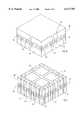
- FIG. 1illustrates a preferred embodiment of integrated circuit device constructed and operative in accordance with a preferred embodiment of the present invention and includes a relatively thin and compact, environmentally protected and mechanically strengthened integrated circuit package 10 having a multiplicity of electrical contacts 12 plated along the edge surfaces 14 thereof.
- contacts 12extend over edge surfaces onto the planar surfaces 16 of the package. This contact arrangement permits both flat surface mounting and edge mounting of package 10 onto a circuit board.
- the integrated circuit package 10may include an integrally formed ground plane (not shown) as well as ground plane contacts 18.
- the integrated circuit package 10may also include one or more thermal bonding pads 19 formed on one or both of the planar surfaces 16 thereof.
- the provision of such thermal bonding pads 19is optional.
- a complete silicon wafer 20 having a plurality of finished dies 22 formed thereon by conventional techniquesis bonded at its active surface 24 to an insulating cover plate 26 via a layer 28 of epoxy.
- the insulating cover plate 26typically comprises glass, alumina, beryllia, sapphire or any other suitable insulative substrate.
- Cover plate 26may be transparent to radiation in a spectral region useful for optical or infrared alignment.
- the complete silicon wafer 20may be formed with an integral ground plane by conventional lithography techniques at any suitable location therein.
- a ground planemay be deposited and configured by conventional techniques over the active surface 24, such that the ground plane lies between active surface 24 and the epoxy layer 28.
- the silicon waferis preferably ground down to a decreased thickness, typically 200 microns, as shown in FIG. 4B. This reduction in wafer thickness is enabled by the additional mechanical strength provided by the bonding thereof of the insulating cover plate 26.
- the waferis scribed along its back surface along predetermined dice lines which separate the individual dies.
- the scribed channels 30are of sufficient depth to reduce the wafer thickness thereunder to typically 100 microns.
- the scribed waferis shown in FIG. 3 and in FIG. 4C.
- the scribed waferis then etched in a conventional silicon etching solution, such as a combination of 24% potassium hydroxide (KOH), 63% water and 13% Isopropanol, so as to etch the silicon down to the field oxide layer, as shown in FIG. 4D and more particularly in FIG. 5.
- a conventional silicon etching solutionsuch as a combination of 24% potassium hydroxide (KOH), 63% water and 13% Isopropanol
- At least one insulating layer, including the field oxide layer,is shown at reference numeral 32 and metal pads are shown at reference numeral 34.
- An over-metal insulating layeris shown at reference numeral 36.
- the ground planeis shown at reference numeral 38.
- the result of the silicon etchingis a plurality of separated dies 40, each of which includes silicon 39 of thickness about 100 microns.
- a second insulating packaging layer 42is bonded over the dies 40 on the side thereof opposite to insulating packaging layer 26.
- a layer 44 of epoxylies between the dies 40 and the layer 42 and epoxy also fills the interstices between dies 40.
- the sandwich of the dies 40, and the first and second insulating packaging layers 26 and 42is then diced along lines 50, lying along the interstices between adjacent dies 40 to define a plurality of pre-packaged integrated circuits. It is a particular feature of the invention that lines 50 are selected such that the edges of the diced chips are distanced from the outer extent of the silicon 39 by at least a distance d, as shown in FIGS. 4E and 5.
- dicing of the sandwich of FIG. 4E along lines 50exposes edges of a multiplicity of pads 34 on the wafer 20, which pad edges, when so exposed, define contact surfaces 51 of dies 40. Dicing of the sandwich of FIG. 4E also exposes edge portions of the ground plane 38 which define ground plane contact surfaces 52.
- FIG. 6illustrates an individual pre-packaged die following dicing.
- the entire integrated circuit deviceis peripherally sealed by epoxy 53 between insulating packaging layers 26 and 42 which define the integrated circuit package.
- all or part of the die or at least the edges thereofis coated with a conductive coating, such as aluminum, as by vacuum deposition.
- a conductive coatingsuch as aluminum, as by vacuum deposition.
- this conductive coatingis selectively etched, as indicated in FIG. 7 to define mutually electrically insulated conductive strips 62, each of which electrically communicates with a different contact surface 51 or 52.
- the thermal bonding pads 19may also be defined at this stage.
- FIG. 8illustrates an alternative embodiment of the present invention wherein all of the contact strips appear on at least one edge 70 thereof, which edge may then be surface mounted onto a printed circuit board, for providing vertical mounting of the integrated circuit device.
- the illustrated embodimentprovides conductive pathways 72 communicating between individual contact surfaces 51 on various edges of the device and contact strips 74 on edge 70. Such pathways may be formed on one or both of the planar surfaces of the integrated circuit package.
- FIG. 9illustrates another optional feature of the present invention.
- substrate isolation of part of an integrated circuit diemay be readily provided by adding extra scribe lines and etching therealong as illustrated in FIGS. 4C and 4D, but within a given die boundary, rather than along die boundaries. Following such scribing and etching the separation between adjacent portions 76 of the silicon substrate is filled with epoxy 78.
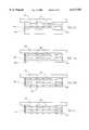
- FIG. 10is an illustration of a multi-die integrated circuit package 100 constructed and operative in accordance with a preferred embodiment of the invention.
- the embodiment of FIG. 10includes a plurality of dies 102, preferably arranged in a stacked arrangement.
- Each die 102may have an identical or different circuit thereon.
- the diesmay be stacked one upon an other in electrically insulative relationship, with or without the interposition of additional insulative layers therebetween.
- the multi-die integrated circuit package 100is relatively thin and compact, environmentally protected and mechanically strengthened and has a multiplicity of electrical contacts 112 plated along the edge surfaces 114 thereof.
- contacts 112extend over edge surfaces onto the planar surfaces 116 of the package. This contact arrangement permits both flat surface mounting and edge mounting of package 100 onto a circuit board.
- the integrated circuit package 100may include one or more integrally formed ground planes (not shown) as well as ground plane contacts 118. Additionally, one or more specific dies, such as an ASIC, for providing complex interconnect functions may be interposed among the stacked integrated circuits.
- the integrated circuit package 100may also include one or more thermal bonding pads 119 formed on one or both of the planar surfaces 116 thereof.
- the provision of such thermal bonding pads 119is optional.
- FIGS. 11A, 11B, 11C,11D, 11E, 11F, 11G, 11H, 11I, 11J, 11K, 11L and 11Mare sectional illustrations of various stages in the manufacture of multi-die integrated circuit devices in accordance with a preferred embodiment of the present invention.
- a complete silicon wafer 120 having a plurality of dies 122 formed thereon by conventional techniquesis bonded at its active surface 124 to an insulating cover plate 126 via a layer 128 of epoxy.
- the insulating cover plate 126typically comprises glass, alumina, beryllia, sapphire or any other suitable insulative substrate.
- the complete silicon wafer 120may be formed with an integral ground plane by conventional techniques at any suitable location therein.
- a ground planemay be deposited and configured by conventional techniques over the active surface 124, such that the ground plane lies between active surface 124 and the epoxy layer 128.
- the silicon waferis preferably ground down to a decreased thickness, typically 200 microns, as shown in FIG. 11B.
- the waferis scribed along its back surface along predetermined dice lines which separate the individual dies.
- the scribed channels 130are of sufficient depth to reduce the wafer thickness thereunder to typically 100 microns.
- the scribed waferis shown in FIG. 11C.
- the scribed waferis then etched in a conventional silicon etching solution, such as that described hereinabove, so as to etch the silicon down to the field oxide layer, as shown in FIG. 11D.
- each dieis configured generally as shown in FIG. 5, described above.
- an additional wafer 150is bonded over scribed and etched dies 122, as illustrated in FIG. 11E, the epoxy 152 which is used for the bonding, filling in the interstices between silicon substrates of adjacent dies 122 and thus providing isolation thereof in addition to that provided by the oxide passivation layer on each die.
- wafer 150is reduced, as shown in FIG. 11F and wafer 150 is scribed and then etched, as shown in FIGS. 11G and 11H respectively and as described hereinabove in connection with FIGS. 4B-4D.
- an additional wafer 160is bonded over scribed and etched wafer 150, as illustrated in FIG. 11I, the epoxy 162 which is used for the bonding, filling in the interstices between silicon substrates of adjacent dies 163 on wafer 150 and thus providing isolation thereof.
- wafer 160is reduced, as shown in FIG. 11J and wafer 160 is scribed and then etched, as shown in FIGS. 11K and 11L respectively and as described hereinabove in connection with FIGS. 4B-4D.
- a second insulating packaging layer 170is bonded thereto, as shown in FIG. 11M.
- a layer 172 of epoxylies between the dies 174 on the last wafer and the layer 170 and the epoxy also fills the interstices between dies 174.
- the sandwich of the plurality of wafers and the first and second insulating packaging layers 126 and 170is then diced along lines lying along the interstices between the adjacent dies on each wafer to define a plurality of pre-packaged integrated circuits.
- dicing of the sandwich of FIGS. 4E and 11Mexposes edges of a multiplicity of pads on the wafers, which pad edges, when so exposed, define contact surfaces. These contact surfaces are preferably subjected to an anti-corrosion treatment. Dicing of the sandwich of FIG. 11M also exposes edge portions of the ground plane which define ground plane contact surfaces, which are also preferably subject to anti-corrosion treatment. Other than the exposed contact surfaces, the entire integrated circuit device is peripherally sealed by epoxy between insulating packaging layers 126 and 170 which define the integrated circuit package.
- a conductive coatingsuch as aluminum, as by vacuum deposition.
- this conductive coatingis selectively etched, as indicated in FIG. 10 to define mutually electrically insulated conductive strips 112, each of which electrically communicates with a different contact surface.
- Conductive strips 112may provide interconnection between the various dies as well as interconnection with external circuits.
- Ground plane contacts 118 and thermal bonding pads 119may also be defined at this stage.
- the conductive layersare preferably nickel coated and may also be gold plated and/or solder coated by conventional techniques. Suitable anti-corrosion treatments may also be provided. It is noted that the stacked integrated circuit package described hereinabove need not necessarily be formed of integrated circuit dies from a single whole wafer or even from the same wafer. The integrated circuit dies which are combined in the stack may be formed individually or in groups by any suitable technique. The integrated circuit dies preferably pass a sorting stage prior to being incorporated in a stack, in order to increase stack yield.
- Improved heat dissipation in the stackmay be achieved by incorporating insulative high thermal conductivity substrates in the die stack.
- FIGS. 12A and 12Billustrate apparatus for producing integrated circuit devices in accordance with a preferred embodiment of the present invention.
- a conventional wafer fabrication facility 180provides complete wafers 20. Individual wafers 20 are bonded on their active surfaces by bonding apparatus 182, preferably having facilities for rotation of the wafer 20, the layer 26 and the epoxy 28 so as to obtain even distribution of the epoxy.
- the bonded wafer(FIG. 3) is thinned at its non-active surface as by grinding apparatus 184, such as Model 32BTGW using 12.5A abrasive, which is commercially available from Speedfam Machines Co. Ltd. of England.
- the waferis then scribed at its non-active surface by scribing apparatus 186 such as a Kulicke & Soffa 775 dicing saw employing an Ni plated diamond loaded blade, producing a result which is shown in FIG. 4C.
- scribing apparatus 186such as a Kulicke & Soffa 775 dicing saw employing an Ni plated diamond loaded blade, producing a result which is shown in FIG. 4C.
- the scribed wafer of FIG. 4Cis then etched in a temperature controlled bath 188 containing a silicon etch solution 190.
- a silicon etch solution 190Commercially available equipment for this purpose include a Chemkleen bath and an WHRV circulator both of which are manufactured by Wafab Inc. of the U.S.A.
- a suitable conventional silicon etching solutionis Isoform Silicon etch, which is commercially available from Micro-Image Technology Ltd. of England.
- the waferis conventionally rinsed after etching.
- the resulting etched waferis shown in FIG. 4D.
- the etched waferis bonded on the non-active side to another protective layer 42 by bonding apparatus 192, which may be essentially the same as apparatus 182, to produce a doubly bonded wafer sandwich as shown in FIG. 4E.
- Dicing apparatus 194which may be identical to apparatus 186, dices the bonded wafer sandwich of FIG. 4E into individual dies.
- the dicing bladeshould be a diamond resinoid blade of thickness 4-12 mils. The resulting dies appear as illustrated generally in FIG. 6.
- the diced diesare then subjected to anti-corrosion treatment in a bath 196, containing a chromating solution 198, such as described in any of the following U.S. Pat. Nos. 2,507,956; 2,851,385 and 2,796,370, the disclosure of which is hereby incorporated by reference.
- Conductive layer deposition apparatus 200which operates by vacuum deposition techniques, such as a Model 903M sputtering machine manufactured by Material Research Corporation of the U.S.A., is employed to produce a conductive layer on one or more surfaces of the die of FIG. 6.
- Configuration of contact stripsis carried out preferably by using conventional electro-deposited photoresist, which is commercially available from DuPont under the brand name Primecoat or from Shipley, under the brand name Eagle.
- the photoresistis applied to the dies in a photoresist bath assembly 202 which is commercially available from DuPont or Shipley.
- the photoresistis preferably laser configured by a suitable laser scanner 204 to define suitable etching patterns.
- the photoresistis then developed in a development bath 206, and then etched in a metal etch solution 208 located in an etching bath 210, thus providing a conductor configuration such as that shown in FIG. 7.
- the exposed conductive strips shown in FIG. 7are then plated, preferably by electroless plating apparatus 212, which is commercially available from Okuno of Japan.
- conductive stripsmay be achieved by techniques other than photolithography. Any suitable technique, such as direct writing, may alternatively be employed.
Landscapes
- Engineering & Computer Science (AREA)
- Microelectronics & Electronic Packaging (AREA)
- Power Engineering (AREA)
- Computer Hardware Design (AREA)
- Physics & Mathematics (AREA)
- Condensed Matter Physics & Semiconductors (AREA)
- General Physics & Mathematics (AREA)
- Manufacturing & Machinery (AREA)
- Dicing (AREA)
Abstract
Description
Claims (17)
Priority Applications (1)
| Application Number | Priority Date | Filing Date | Title |
|---|---|---|---|
| US08/681,598US6117707A (en) | 1994-07-13 | 1996-07-29 | Methods of producing integrated circuit devices |
Applications Claiming Priority (2)
| Application Number | Priority Date | Filing Date | Title |
|---|---|---|---|
| US08/274,251US5547906A (en) | 1992-09-14 | 1994-07-13 | Methods for producing integrated circuit devices |
| US08/681,598US6117707A (en) | 1994-07-13 | 1996-07-29 | Methods of producing integrated circuit devices |
Related Parent Applications (1)
| Application Number | Title | Priority Date | Filing Date |
|---|---|---|---|
| US08/274,251ContinuationUS5547906A (en) | 1992-09-14 | 1994-07-13 | Methods for producing integrated circuit devices |
Publications (1)
| Publication Number | Publication Date |
|---|---|
| US6117707Atrue US6117707A (en) | 2000-09-12 |
Family
ID=23047442
Family Applications (1)
| Application Number | Title | Priority Date | Filing Date |
|---|---|---|---|
| US08/681,598Expired - LifetimeUS6117707A (en) | 1994-07-13 | 1996-07-29 | Methods of producing integrated circuit devices |
Country Status (1)
| Country | Link |
|---|---|
| US (1) | US6117707A (en) |
Cited By (48)
| Publication number | Priority date | Publication date | Assignee | Title |
|---|---|---|---|---|
| US6196096B1 (en) | 1996-11-12 | 2001-03-06 | Micron Technology, Inc. | Method for sawing wafers employing multiple indexing techniques for multiple die dimensions |
| US6341070B1 (en)* | 1998-07-28 | 2002-01-22 | Ho-Yuan Yu | Wafer-scale packing processes for manufacturing integrated circuit (IC) packages |
| US20020117753A1 (en)* | 2001-02-23 | 2002-08-29 | Lee Michael G. | Three dimensional packaging |
| US20020184756A1 (en)* | 2001-05-31 | 2002-12-12 | Infineon Technologies Ag | Wiring process |
| US6493934B2 (en) | 1996-11-12 | 2002-12-17 | Salman Akram | Method for sawing wafers employing multiple indexing techniques for multiple die dimensions |
| US20030127654A1 (en)* | 2000-02-15 | 2003-07-10 | Dominik Eisert | Semiconductor component which emits radiation, and method for producing the same |
| US20030164502A1 (en)* | 2000-05-23 | 2003-09-04 | Johannes Baur | Optoelectronic component and a method for producing the same |
| US20030216010A1 (en)* | 2002-05-20 | 2003-11-20 | Eugene Atlas | Forming a multi segment integrated circuit with isolated substrates |
| US20040021214A1 (en)* | 2002-04-16 | 2004-02-05 | Avner Badehi | Electro-optic integrated circuits with connectors and methods for the production thereof |
| US20040031476A1 (en)* | 2001-06-06 | 2004-02-19 | Farnworth Warren M. | Group encapsulated dicing chuck |
| US20040251545A1 (en)* | 2003-06-10 | 2004-12-16 | Su Tao | Semiconductor chip with bumps and method for manufacturing the same |
| US20050003565A1 (en)* | 2000-02-15 | 2005-01-06 | Osram Opto Semiconductors Gmbh, A Germany Corporat | Radiation emitting semiconductor device |
| US6864116B1 (en) | 2003-10-01 | 2005-03-08 | Optopac, Inc. | Electronic package of photo-sensing semiconductor devices, and the fabrication and assembly thereof |
| US20050073017A1 (en)* | 2003-10-01 | 2005-04-07 | Deok-Hoon Kim | Electronic package of photo-image sensors in cellular phone camera modules, and the fabrication and assembly thereof |
| US20050158899A1 (en)* | 2002-03-18 | 2005-07-21 | Sarcos Investments Lc | Miniaturized imaging device with integrated circuit connector system |
| US6943424B1 (en) | 2004-05-06 | 2005-09-13 | Optopac, Inc. | Electronic package having a patterned layer on backside of its substrate, and the fabrication thereof |
| US20050224938A1 (en)* | 2004-04-12 | 2005-10-13 | Deok-Hoon Kim | Electronic package having a sealing structure on predetermined area, and the method thereof |
| US20050233498A1 (en)* | 2002-04-29 | 2005-10-20 | Texas Instruments Inc. | MEMS device wafer-level package |
| US20060022289A1 (en)* | 2002-04-16 | 2006-02-02 | Xloom Photonics, Ltd. | Electro-optical circuitry having integrated connector and methods for the production thereof |
| US20060043513A1 (en)* | 2004-09-02 | 2006-03-02 | Deok-Hoon Kim | Method of making camera module in wafer level |
| US20060097335A1 (en)* | 2004-11-08 | 2006-05-11 | Deok-Hoon Kim | Electronic package for image sensor, and the packaging method thereof |
| US20060138626A1 (en)* | 2004-12-29 | 2006-06-29 | Tessera, Inc. | Microelectronic packages using a ceramic substrate having a window and a conductive surface region |
| US20060202314A1 (en)* | 2005-03-09 | 2006-09-14 | Advanced Semiconductor Engineering, Inc. | Semiconductor package and method for manufacturing the same |
| US20070042562A1 (en)* | 1998-02-06 | 2007-02-22 | Tessera Technologies Hungary Kft. | Integrated circuit device |
| US20070047377A1 (en)* | 2005-08-12 | 2007-03-01 | Samsung Electronics Co., Ltd. | Printed circuit board for memory module, method of manufacturing the same and memory module/socket assembly |
| US20080106288A1 (en)* | 2006-11-07 | 2008-05-08 | Apple Inc. | Circuit boards including removable test point portions and configurable testing platforms |
| US20080213977A1 (en)* | 2007-03-01 | 2008-09-04 | Wyant M Todd | Vacuum expansion of integrated circuits at sort |
| US20080315424A1 (en)* | 2001-03-30 | 2008-12-25 | Megica Corporation | Structure and manufactruing method of chip scale package |
| US20090034085A1 (en)* | 2003-10-15 | 2009-02-05 | Xloom Communications, Ltd. | Electro-optical circuitry having integrated connector and methods for the production thereof |
| US20090093137A1 (en)* | 2007-10-08 | 2009-04-09 | Xloom Communications, (Israel) Ltd. | Optical communications module |
| US20090149002A1 (en)* | 2007-12-06 | 2009-06-11 | Disco Corporation | Method of forming a modified layer in a substrate |
| US20090213542A1 (en)* | 2008-02-22 | 2009-08-27 | Seagate Technology Llc | Flex circuit assembly with thermal energy dissipation |
| US20090251873A1 (en)* | 2008-04-02 | 2009-10-08 | Sun-Wen Cyrus Cheng | Surface Mount Power Module Dual Footprint |
| US7787939B2 (en) | 2002-03-18 | 2010-08-31 | Sterling Lc | Miniaturized imaging device including utility aperture and SSID |
| US7835074B2 (en) | 2007-06-05 | 2010-11-16 | Sterling Lc | Mini-scope for multi-directional imaging |
| US7960272B2 (en) | 2002-10-24 | 2011-06-14 | Megica Corporation | Method for fabricating thermal compliant semiconductor chip wiring structure for chip scale packaging |
| US7969659B2 (en) | 2008-01-11 | 2011-06-28 | Sterling Lc | Grin lens microscope system |
| US8436636B2 (en) | 2006-10-10 | 2013-05-07 | Apple Inc. | Methods and apparatuses for testing circuit boards |
| US8486735B2 (en) | 2008-07-30 | 2013-07-16 | Raytheon Company | Method and device for incremental wavelength variation to analyze tissue |
| US8614768B2 (en) | 2002-03-18 | 2013-12-24 | Raytheon Company | Miniaturized imaging device including GRIN lens optically coupled to SSID |
| US8649183B2 (en) | 2011-02-10 | 2014-02-11 | Mulpin Research Laboratories, Ltd. | Electronic assembly |
| US8669777B2 (en) | 2010-10-27 | 2014-03-11 | Seagate Technology Llc | Assessing connection joint coverage between a device and a printed circuit board |
| US8690762B2 (en) | 2008-06-18 | 2014-04-08 | Raytheon Company | Transparent endoscope head defining a focal length |
| US8717428B2 (en) | 2009-10-01 | 2014-05-06 | Raytheon Company | Light diffusion apparatus |
| US8828028B2 (en) | 2009-11-03 | 2014-09-09 | Raytheon Company | Suture device and method for closing a planar opening |
| US9060704B2 (en) | 2008-11-04 | 2015-06-23 | Sarcos Lc | Method and device for wavelength shifted imaging |
| US9144664B2 (en) | 2009-10-01 | 2015-09-29 | Sarcos Lc | Method and apparatus for manipulating movement of a micro-catheter |
| US9661996B2 (en) | 2009-10-01 | 2017-05-30 | Sarcos Lc | Needle delivered imaging device |
Citations (25)
| Publication number | Priority date | Publication date | Assignee | Title |
|---|---|---|---|---|
| US2507956A (en)* | 1947-11-01 | 1950-05-16 | Lithographic Technical Foundat | Process of coating aluminum |
| US2796370A (en)* | 1955-03-04 | 1957-06-18 | Charles W Ostrander | Composition and method for producing corrosion resistant protective coating on aluminum and aluminum alloys |
| US2851385A (en)* | 1952-04-03 | 1958-09-09 | Amchem Prod | Process and composition for coating aluminum surfaces |
| DE1591105A1 (en)* | 1967-12-06 | 1970-09-24 | Itt Ind Gmbh Deutsche | Method for manufacturing solid state circuits |
| US3644801A (en)* | 1971-01-21 | 1972-02-22 | Gary S Sheldon | Semiconductor passivating process and product |
| US4383886A (en)* | 1980-11-14 | 1983-05-17 | Tokyo Shibaura Denki Kabushiki Kaisha | Method of manufacturing a semiconductor element |
| WO1985002283A1 (en)* | 1983-11-07 | 1985-05-23 | Irvine Sensors Corporation | Detector array module-structure and fabrication |
| EP0211609A2 (en)* | 1985-08-01 | 1987-02-25 | Unilever Plc | Chemically sensitive semiconductor devices and their production |
| US4794092A (en)* | 1987-11-18 | 1988-12-27 | Grumman Aerospace Corporation | Single wafer moated process |
| US4862249A (en)* | 1987-04-17 | 1989-08-29 | Xoc Devices, Inc. | Packaging system for stacking integrated circuits |
| JPH0217644A (en)* | 1988-07-06 | 1990-01-22 | Hitachi Ltd | Integrated circuit |
| US4900695A (en)* | 1986-12-17 | 1990-02-13 | Hitachi, Ltd. | Semiconductor integrated circuit device and process for producing the same |
| US4933898A (en)* | 1989-01-12 | 1990-06-12 | General Instrument Corporation | Secure integrated circuit chip with conductive shield |
| JPH02191358A (en)* | 1989-01-19 | 1990-07-27 | Toshiba Corp | Processing method of semiconductor elements |
| US4971930A (en)* | 1985-12-20 | 1990-11-20 | Sgs Microelectronics S.P.A. | EPROM semiconductor device erasable with ultraviolet rays and manufacturing process thereof |
| US4984358A (en)* | 1989-03-10 | 1991-01-15 | Microelectronics And Computer Technology Corporation | Method of assembling stacks of integrated circuit dies |
| US5104820A (en)* | 1989-07-07 | 1992-04-14 | Irvine Sensors Corporation | Method of fabricating electronic circuitry unit containing stacked IC layers having lead rerouting |
| EP0490739A1 (en)* | 1990-12-11 | 1992-06-17 | Thomson-Csf | Interconnection method and device for three-dimensional integrated circuits |
| US5126286A (en)* | 1990-10-05 | 1992-06-30 | Micron Technology, Inc. | Method of manufacturing edge connected semiconductor die |
| US5147815A (en)* | 1990-05-14 | 1992-09-15 | Motorola, Inc. | Method for fabricating a multichip semiconductor device having two interdigitated leadframes |
| US5185295A (en)* | 1990-05-16 | 1993-02-09 | Kabushiki Kaisha Toshiba | Method for dicing semiconductor substrates using a laser scribing and dual etch process |
| US5266833A (en)* | 1992-03-30 | 1993-11-30 | Capps David F | Integrated circuit bus structure |
| US5292686A (en)* | 1991-08-21 | 1994-03-08 | Triquint Semiconductor, Inc. | Method of forming substrate vias in a GaAs wafer |
| US5376235A (en)* | 1993-07-15 | 1994-12-27 | Micron Semiconductor, Inc. | Method to eliminate corrosion in conductive elements |
| US5455455A (en)* | 1992-09-14 | 1995-10-03 | Badehi; Peirre | Methods for producing packaged integrated circuit devices and packaged integrated circuit devices produced thereby |
- 1996
- 1996-07-29USUS08/681,598patent/US6117707A/ennot_activeExpired - Lifetime
Patent Citations (25)
| Publication number | Priority date | Publication date | Assignee | Title |
|---|---|---|---|---|
| US2507956A (en)* | 1947-11-01 | 1950-05-16 | Lithographic Technical Foundat | Process of coating aluminum |
| US2851385A (en)* | 1952-04-03 | 1958-09-09 | Amchem Prod | Process and composition for coating aluminum surfaces |
| US2796370A (en)* | 1955-03-04 | 1957-06-18 | Charles W Ostrander | Composition and method for producing corrosion resistant protective coating on aluminum and aluminum alloys |
| DE1591105A1 (en)* | 1967-12-06 | 1970-09-24 | Itt Ind Gmbh Deutsche | Method for manufacturing solid state circuits |
| US3644801A (en)* | 1971-01-21 | 1972-02-22 | Gary S Sheldon | Semiconductor passivating process and product |
| US4383886A (en)* | 1980-11-14 | 1983-05-17 | Tokyo Shibaura Denki Kabushiki Kaisha | Method of manufacturing a semiconductor element |
| WO1985002283A1 (en)* | 1983-11-07 | 1985-05-23 | Irvine Sensors Corporation | Detector array module-structure and fabrication |
| EP0211609A2 (en)* | 1985-08-01 | 1987-02-25 | Unilever Plc | Chemically sensitive semiconductor devices and their production |
| US4971930A (en)* | 1985-12-20 | 1990-11-20 | Sgs Microelectronics S.P.A. | EPROM semiconductor device erasable with ultraviolet rays and manufacturing process thereof |
| US4900695A (en)* | 1986-12-17 | 1990-02-13 | Hitachi, Ltd. | Semiconductor integrated circuit device and process for producing the same |
| US4862249A (en)* | 1987-04-17 | 1989-08-29 | Xoc Devices, Inc. | Packaging system for stacking integrated circuits |
| US4794092A (en)* | 1987-11-18 | 1988-12-27 | Grumman Aerospace Corporation | Single wafer moated process |
| JPH0217644A (en)* | 1988-07-06 | 1990-01-22 | Hitachi Ltd | Integrated circuit |
| US4933898A (en)* | 1989-01-12 | 1990-06-12 | General Instrument Corporation | Secure integrated circuit chip with conductive shield |
| JPH02191358A (en)* | 1989-01-19 | 1990-07-27 | Toshiba Corp | Processing method of semiconductor elements |
| US4984358A (en)* | 1989-03-10 | 1991-01-15 | Microelectronics And Computer Technology Corporation | Method of assembling stacks of integrated circuit dies |
| US5104820A (en)* | 1989-07-07 | 1992-04-14 | Irvine Sensors Corporation | Method of fabricating electronic circuitry unit containing stacked IC layers having lead rerouting |
| US5147815A (en)* | 1990-05-14 | 1992-09-15 | Motorola, Inc. | Method for fabricating a multichip semiconductor device having two interdigitated leadframes |
| US5185295A (en)* | 1990-05-16 | 1993-02-09 | Kabushiki Kaisha Toshiba | Method for dicing semiconductor substrates using a laser scribing and dual etch process |
| US5126286A (en)* | 1990-10-05 | 1992-06-30 | Micron Technology, Inc. | Method of manufacturing edge connected semiconductor die |
| EP0490739A1 (en)* | 1990-12-11 | 1992-06-17 | Thomson-Csf | Interconnection method and device for three-dimensional integrated circuits |
| US5292686A (en)* | 1991-08-21 | 1994-03-08 | Triquint Semiconductor, Inc. | Method of forming substrate vias in a GaAs wafer |
| US5266833A (en)* | 1992-03-30 | 1993-11-30 | Capps David F | Integrated circuit bus structure |
| US5455455A (en)* | 1992-09-14 | 1995-10-03 | Badehi; Peirre | Methods for producing packaged integrated circuit devices and packaged integrated circuit devices produced thereby |
| US5376235A (en)* | 1993-07-15 | 1994-12-27 | Micron Semiconductor, Inc. | Method to eliminate corrosion in conductive elements |
Non-Patent Citations (5)
| Title |
|---|
| Background Information R&D 100 Technology s Brightest Stars, Tessera System Building Blocks, San Jose, CA. 1993.* |
| Background Information--R&D 100 Technology's Brightest Stars, Tessera System Building Blocks, San Jose, CA. 1993. |
| D. Richmould, Micro SMT Integrated Circuit Technical White Paper, Micro SMT Inc. Jan. 25, 1993, pp. 1 15.* |
| D. Richmould, Micro SMT Integrated Circuit Technical White Paper, Micro SMT Inc. Jan. 25, 1993, pp. 1-15. |
| Tessera Compliant Chip, Technology Overview, Tessera System Building Blocks, San Jose, Ca. 1993.* |
Cited By (111)
| Publication number | Priority date | Publication date | Assignee | Title |
|---|---|---|---|---|
| US6687990B2 (en) | 1996-11-12 | 2004-02-10 | Micron Technology, Inc. | Sawing method employing multiple indexing techniques and semiconductor device structures fabricated thereby |
| US6255196B1 (en)* | 1996-11-12 | 2001-07-03 | Micron Technology, Inc. | Method for sawing wafers employing multiple indexing techniques for multiple die dimensions |
| US6279563B1 (en) | 1996-11-12 | 2001-08-28 | Micron Technology, Inc. | Method for sawing wafers employing multiple indexing techniques for multiple die dimensions |
| US7387119B2 (en) | 1996-11-12 | 2008-06-17 | Micron Technology, Inc. | Dicing saw with variable indexing capability |
| US6401580B1 (en) | 1996-11-12 | 2002-06-11 | Micron Technology, Inc. | Method for sawing wafers employing multiple indexing techniques for multiple die dimensions |
| US6423616B2 (en) | 1996-11-12 | 2002-07-23 | Micron Technology, Inc. | Method for sawing wafers employing multiple indexing techniques for multiple die dimensions |
| US6427676B2 (en) | 1996-11-12 | 2002-08-06 | Micron Technology, Inc. | Method for sawing wafers employing multiple indexing techniques for multiple die dimensions |
| US6196096B1 (en) | 1996-11-12 | 2001-03-06 | Micron Technology, Inc. | Method for sawing wafers employing multiple indexing techniques for multiple die dimensions |
| US6459105B2 (en) | 1996-11-12 | 2002-10-01 | Micron Technology, Inc. | Apparatus for sawing wafers employing multiple indexing techniques for multiple die dimensions |
| US6932077B2 (en) | 1996-11-12 | 2005-08-23 | Micron Technology, Inc. | Method for sawing wafers employing multiple indexing techniques for multiple die dimensions and dicing apparatus |
| US6493934B2 (en) | 1996-11-12 | 2002-12-17 | Salman Akram | Method for sawing wafers employing multiple indexing techniques for multiple die dimensions |
| US6578458B1 (en) | 1996-11-12 | 2003-06-17 | Micron Technology, Inc. | Method for sawing wafers employing multiple indexing techniques for multiple die dimensions |
| US6897571B2 (en) | 1996-11-12 | 2005-05-24 | Micron Technology, Inc. | Method for sawing wafers employing multiple indexing techniques for multiple die dimensions |
| US6691696B2 (en) | 1996-11-12 | 2004-02-17 | Micron Technology, Inc. | Method for sawing wafers employing multiple indexing techniques for multiple die dimensions |
| US6631662B2 (en) | 1996-11-12 | 2003-10-14 | Micron Technology, Inc. | Apparatus for sawing wafers employing multiple indexing techniques for multiple die dimensions |
| US7781240B2 (en)* | 1998-02-06 | 2010-08-24 | Tessera Technologies Hungary Kft. | Integrated circuit device |
| US9530945B2 (en) | 1998-02-06 | 2016-12-27 | Invensas Corporation | Integrated circuit device |
| US20070042562A1 (en)* | 1998-02-06 | 2007-02-22 | Tessera Technologies Hungary Kft. | Integrated circuit device |
| US8592831B2 (en) | 1998-02-06 | 2013-11-26 | Invensas Corp. | Integrated circuit device |
| US6341070B1 (en)* | 1998-07-28 | 2002-01-22 | Ho-Yuan Yu | Wafer-scale packing processes for manufacturing integrated circuit (IC) packages |
| US7195942B2 (en)* | 2000-02-15 | 2007-03-27 | Osram Gmbh | Radiation emitting semiconductor device |
| US20050003565A1 (en)* | 2000-02-15 | 2005-01-06 | Osram Opto Semiconductors Gmbh, A Germany Corporat | Radiation emitting semiconductor device |
| US7205578B2 (en) | 2000-02-15 | 2007-04-17 | Osram Gmbh | Semiconductor component which emits radiation, and method for producing the same |
| US20070145402A1 (en)* | 2000-02-15 | 2007-06-28 | Dominik Eisert | Semiconductor component which emits radiation, and method for producing the same |
| US20030127654A1 (en)* | 2000-02-15 | 2003-07-10 | Dominik Eisert | Semiconductor component which emits radiation, and method for producing the same |
| US20030164502A1 (en)* | 2000-05-23 | 2003-09-04 | Johannes Baur | Optoelectronic component and a method for producing the same |
| US20020117753A1 (en)* | 2001-02-23 | 2002-08-29 | Lee Michael G. | Three dimensional packaging |
| US8748227B2 (en) | 2001-03-30 | 2014-06-10 | Megit Acquisition Corp. | Method of fabricating chip package |
| US20080315424A1 (en)* | 2001-03-30 | 2008-12-25 | Megica Corporation | Structure and manufactruing method of chip scale package |
| US8426982B2 (en) | 2001-03-30 | 2013-04-23 | Megica Corporation | Structure and manufacturing method of chip scale package |
| US9018774B2 (en) | 2001-03-30 | 2015-04-28 | Qualcomm Incorporated | Chip package |
| US8912666B2 (en) | 2001-03-30 | 2014-12-16 | Qualcomm Incorporated | Structure and manufacturing method of chip scale package |
| US20020184756A1 (en)* | 2001-05-31 | 2002-12-12 | Infineon Technologies Ag | Wiring process |
| US7028399B2 (en)* | 2001-05-31 | 2006-04-18 | Infineon Technologies Ag | Wiring process |
| US20050186761A1 (en)* | 2001-06-06 | 2005-08-25 | Farnworth Warren M. | Group encapsulated dicing chuck |
| US20040031476A1 (en)* | 2001-06-06 | 2004-02-19 | Farnworth Warren M. | Group encapsulated dicing chuck |
| US20060065262A1 (en)* | 2001-06-06 | 2006-03-30 | Farnworth Warren M | Group encapsulated dicing chuck |
| US20070068504A1 (en)* | 2001-06-06 | 2007-03-29 | Farnworth Warren M | Group encapsulated dicing chuck |
| US20070062511A1 (en)* | 2001-06-06 | 2007-03-22 | Farnworth Warren M | Group encapsulated dicing chuck |
| US7166537B2 (en) | 2002-03-18 | 2007-01-23 | Sarcos Investments Lc | Miniaturized imaging device with integrated circuit connector system |
| US7629659B2 (en) | 2002-03-18 | 2009-12-08 | Sterling Lc | Miniaturized imaging device with integrated circuit connector system |
| US20050158899A1 (en)* | 2002-03-18 | 2005-07-21 | Sarcos Investments Lc | Miniaturized imaging device with integrated circuit connector system |
| US7591780B2 (en) | 2002-03-18 | 2009-09-22 | Sterling Lc | Miniaturized imaging device with integrated circuit connector system |
| US7787939B2 (en) | 2002-03-18 | 2010-08-31 | Sterling Lc | Miniaturized imaging device including utility aperture and SSID |
| US8614768B2 (en) | 2002-03-18 | 2013-12-24 | Raytheon Company | Miniaturized imaging device including GRIN lens optically coupled to SSID |
| US20090246905A1 (en)* | 2002-04-16 | 2009-10-01 | Xloom Communications, Inc. | Electro-optic integrated circuits and methods for the production thereof |
| US20060022289A1 (en)* | 2002-04-16 | 2006-02-02 | Xloom Photonics, Ltd. | Electro-optical circuitry having integrated connector and methods for the production thereof |
| US20090154873A1 (en)* | 2002-04-16 | 2009-06-18 | Xloom Communications, (Israel) Ltd. | Electro-optic integrated circuits with connectors and methods for the production thereof |
| US20060145279A1 (en)* | 2002-04-16 | 2006-07-06 | Xloom Photonics, Ltd. | Electro-optic integrated circuits with connectors and methods for the production thereof |
| US8043877B2 (en) | 2002-04-16 | 2011-10-25 | Xloom Communications, Ltd. | Electro-optic integrated circuits and methods for the production thereof |
| US20040021214A1 (en)* | 2002-04-16 | 2004-02-05 | Avner Badehi | Electro-optic integrated circuits with connectors and methods for the production thereof |
| US7226810B2 (en) | 2002-04-29 | 2007-06-05 | Texas Instruments Incorporated | MEMS device wafer-level package |
| US20070228540A1 (en)* | 2002-04-29 | 2007-10-04 | Texas Instruments Incorporated | MEMS Device Wafer-Level Package |
| US20050233498A1 (en)* | 2002-04-29 | 2005-10-20 | Texas Instruments Inc. | MEMS device wafer-level package |
| US7466018B2 (en) | 2002-04-29 | 2008-12-16 | Texas Instruments Incorporated | MEMS device wafer-level package |
| US20030216010A1 (en)* | 2002-05-20 | 2003-11-20 | Eugene Atlas | Forming a multi segment integrated circuit with isolated substrates |
| US7960272B2 (en) | 2002-10-24 | 2011-06-14 | Megica Corporation | Method for fabricating thermal compliant semiconductor chip wiring structure for chip scale packaging |
| US8334588B2 (en) | 2002-10-24 | 2012-12-18 | Megica Corporation | Circuit component with conductive layer structure |
| US7037759B2 (en) | 2003-06-10 | 2006-05-02 | Advanced Semiconductor Engineering, Inc. | Semiconductor package and method for manufacturing the same |
| US20060183313A1 (en)* | 2003-06-10 | 2006-08-17 | Su Tao | Semiconductor package and method for manufacturing the same |
| US20040251545A1 (en)* | 2003-06-10 | 2004-12-16 | Su Tao | Semiconductor chip with bumps and method for manufacturing the same |
| US7321168B2 (en) | 2003-06-10 | 2008-01-22 | Advanced Semiconductor Engineering, Inc. | Semiconductor package and method for manufacturing the same |
| US20050208702A1 (en)* | 2003-10-01 | 2005-09-22 | Deok-Hoon Kim | Electronic package of photo-image sensors in cellular phone camera modules, and the fabrication and assembly thereof |
| US6943423B2 (en) | 2003-10-01 | 2005-09-13 | Optopac, Inc. | Electronic package of photo-image sensors in cellular phone camera modules, and the fabrication and assembly thereof |
| US7038287B2 (en) | 2003-10-01 | 2006-05-02 | Optopac, Inc. | Electronic package of photo-sensing semiconductor devices, and the fabrication and assembly thereof |
| US6864116B1 (en) | 2003-10-01 | 2005-03-08 | Optopac, Inc. | Electronic package of photo-sensing semiconductor devices, and the fabrication and assembly thereof |
| US20050073017A1 (en)* | 2003-10-01 | 2005-04-07 | Deok-Hoon Kim | Electronic package of photo-image sensors in cellular phone camera modules, and the fabrication and assembly thereof |
| US7291518B2 (en) | 2003-10-01 | 2007-11-06 | Optopac, Inc. | Electronic package of photo-image sensors in cellular phone camera modules, and the fabrication and assembly thereof |
| US20050098802A1 (en)* | 2003-10-01 | 2005-05-12 | Kim Deok H. | Electronic package of photo-sensing semiconductor devices, and the fabrication and assembly thereof |
| US20090034085A1 (en)* | 2003-10-15 | 2009-02-05 | Xloom Communications, Ltd. | Electro-optical circuitry having integrated connector and methods for the production thereof |
| US7538358B2 (en) | 2003-10-15 | 2009-05-26 | Xloom Communications, Ltd. | Electro-optical circuitry having integrated connector and methods for the production thereof |
| US7122874B2 (en) | 2004-04-12 | 2006-10-17 | Optopac, Inc. | Electronic package having a sealing structure on predetermined area, and the method thereof |
| US20050224938A1 (en)* | 2004-04-12 | 2005-10-13 | Deok-Hoon Kim | Electronic package having a sealing structure on predetermined area, and the method thereof |
| US6943424B1 (en) | 2004-05-06 | 2005-09-13 | Optopac, Inc. | Electronic package having a patterned layer on backside of its substrate, and the fabrication thereof |
| US20060043513A1 (en)* | 2004-09-02 | 2006-03-02 | Deok-Hoon Kim | Method of making camera module in wafer level |
| US7141869B2 (en) | 2004-11-08 | 2006-11-28 | Optopac, Inc. | Electronic package for image sensor, and the packaging method thereof |
| US20060097335A1 (en)* | 2004-11-08 | 2006-05-11 | Deok-Hoon Kim | Electronic package for image sensor, and the packaging method thereof |
| US20060138626A1 (en)* | 2004-12-29 | 2006-06-29 | Tessera, Inc. | Microelectronic packages using a ceramic substrate having a window and a conductive surface region |
| US7285434B2 (en) | 2005-03-09 | 2007-10-23 | Advanced Semiconductor Engineering, Inc. | Semiconductor package and method for manufacturing the same |
| US20080048312A1 (en)* | 2005-03-09 | 2008-02-28 | Advanced Semiconductor Engineering, Inc. | Semiconductor package and method for manufacturing the same |
| US20060202314A1 (en)* | 2005-03-09 | 2006-09-14 | Advanced Semiconductor Engineering, Inc. | Semiconductor package and method for manufacturing the same |
| US20070047377A1 (en)* | 2005-08-12 | 2007-03-01 | Samsung Electronics Co., Ltd. | Printed circuit board for memory module, method of manufacturing the same and memory module/socket assembly |
| US8189342B2 (en)* | 2005-08-12 | 2012-05-29 | Samsung Electronics Co., Ltd. | Printed circuit board for memory module, method of manufacturing the same and memory module/socket assembly |
| US8436636B2 (en) | 2006-10-10 | 2013-05-07 | Apple Inc. | Methods and apparatuses for testing circuit boards |
| US20080106288A1 (en)* | 2006-11-07 | 2008-05-08 | Apple Inc. | Circuit boards including removable test point portions and configurable testing platforms |
| US9513314B2 (en) | 2006-11-07 | 2016-12-06 | Apple Inc. | Configurable testing platforms for circuit boards with removable test point portions |
| US8362793B2 (en)* | 2006-11-07 | 2013-01-29 | Apple Inc. | Circuit boards including removable test point portions and configurable testing platforms |
| US7651925B2 (en) | 2007-03-01 | 2010-01-26 | Delphi Technologies, Inc. | Vacuum expansion of integrated circuits at sort |
| US20080213977A1 (en)* | 2007-03-01 | 2008-09-04 | Wyant M Todd | Vacuum expansion of integrated circuits at sort |
| US8358462B2 (en) | 2007-06-05 | 2013-01-22 | Jacobsen Stephen C | Mini-scope for multi-directional imaging |
| US7835074B2 (en) | 2007-06-05 | 2010-11-16 | Sterling Lc | Mini-scope for multi-directional imaging |
| US20090093137A1 (en)* | 2007-10-08 | 2009-04-09 | Xloom Communications, (Israel) Ltd. | Optical communications module |
| US20090149002A1 (en)* | 2007-12-06 | 2009-06-11 | Disco Corporation | Method of forming a modified layer in a substrate |
| US7927974B2 (en)* | 2007-12-06 | 2011-04-19 | Disco Corporation | Method of forming a modified layer in a substrate |
| US7969659B2 (en) | 2008-01-11 | 2011-06-28 | Sterling Lc | Grin lens microscope system |
| US20090213542A1 (en)* | 2008-02-22 | 2009-08-27 | Seagate Technology Llc | Flex circuit assembly with thermal energy dissipation |
| US7952834B2 (en) | 2008-02-22 | 2011-05-31 | Seagate Technology Llc | Flex circuit assembly with thermal energy dissipation |
| US8319114B2 (en)* | 2008-04-02 | 2012-11-27 | Densel Lambda K.K. | Surface mount power module dual footprint |
| US20090251873A1 (en)* | 2008-04-02 | 2009-10-08 | Sun-Wen Cyrus Cheng | Surface Mount Power Module Dual Footprint |
| US9521946B2 (en) | 2008-06-18 | 2016-12-20 | Sarcos Lc | Transparent endoscope head defining a focal length |
| US8690762B2 (en) | 2008-06-18 | 2014-04-08 | Raytheon Company | Transparent endoscope head defining a focal length |
| US8486735B2 (en) | 2008-07-30 | 2013-07-16 | Raytheon Company | Method and device for incremental wavelength variation to analyze tissue |
| US9259142B2 (en) | 2008-07-30 | 2016-02-16 | Sarcos Lc | Method and device for incremental wavelength variation to analyze tissue |
| US9060704B2 (en) | 2008-11-04 | 2015-06-23 | Sarcos Lc | Method and device for wavelength shifted imaging |
| US9717418B2 (en) | 2008-11-04 | 2017-08-01 | Sarcos Lc | Method and device for wavelength shifted imaging |
| US9144664B2 (en) | 2009-10-01 | 2015-09-29 | Sarcos Lc | Method and apparatus for manipulating movement of a micro-catheter |
| US8717428B2 (en) | 2009-10-01 | 2014-05-06 | Raytheon Company | Light diffusion apparatus |
| US9661996B2 (en) | 2009-10-01 | 2017-05-30 | Sarcos Lc | Needle delivered imaging device |
| US8828028B2 (en) | 2009-11-03 | 2014-09-09 | Raytheon Company | Suture device and method for closing a planar opening |
| US8669777B2 (en) | 2010-10-27 | 2014-03-11 | Seagate Technology Llc | Assessing connection joint coverage between a device and a printed circuit board |
| US8649183B2 (en) | 2011-02-10 | 2014-02-11 | Mulpin Research Laboratories, Ltd. | Electronic assembly |
Similar Documents
| Publication | Publication Date | Title |
|---|---|---|
| US6117707A (en) | Methods of producing integrated circuit devices | |
| US5547906A (en) | Methods for producing integrated circuit devices | |
| US6040235A (en) | Methods and apparatus for producing integrated circuit devices | |
| US6746898B2 (en) | Integrated chip package structure using silicon substrate and method of manufacturing the same | |
| US8119446B2 (en) | Integrated chip package structure using metal substrate and method of manufacturing the same | |
| US5481133A (en) | Three-dimensional multichip package | |
| US6972480B2 (en) | Methods and apparatus for packaging integrated circuit devices | |
| KR100419352B1 (en) | Chip scale surface mount package for semiconductor device and process of fabricating the same | |
| US8835221B2 (en) | Integrated chip package structure using ceramic substrate and method of manufacturing the same | |
| US20030080398A1 (en) | Packaged integrated circuits and methods of producing thereof | |
| US20030006493A1 (en) | Semiconductor device and manufacturing method thereof | |
| KR20030045696A (en) | Semiconductor device, multichip module and method for manufacturing multichip module | |
| JP2003086762A (en) | Semiconductor device and manufacturing method thereof | |
| US20020192875A1 (en) | Method for fabricating a circuit device | |
| EP4160663A1 (en) | A type of bumpless and wireless semiconductor device | |
| TW202531398A (en) | Ultra-thin packaging component and manufacturing method | |
| KR20210152772A (en) | Semiconductor package | |
| TW200423364A (en) | Semiconductor package and manufacturing method thereof |
Legal Events
| Date | Code | Title | Description |
|---|---|---|---|
| STCF | Information on status: patent grant | Free format text:PATENTED CASE | |
| FPAY | Fee payment | Year of fee payment:4 | |
| AS | Assignment | Owner name:SHELLCASE LTD., ISRAEL Free format text:ASSIGNMENT OF ASSIGNORS INTEREST;ASSIGNOR:BADEHI, PIERRE;REEL/FRAME:017262/0757 Effective date:19980331 | |
| AS | Assignment | Owner name:TESSERA TECHNOLOGIES HUNGARY KFT., HUNGARY Free format text:ASSIGNMENT OF ASSIGNORS INTEREST;ASSIGNOR:SHELLCASE LTD., ALSO SOMETIMES KNOWN AS SHELLCASE, LTD.;REEL/FRAME:017507/0691 Effective date:20060330 | |
| AS | Assignment | Owner name:TESSERA TECHNOLOGIES HUNGARY KFT., HUNGARY Free format text:RE-RECORD ASSIGNMENT TO CORRECT STREET ADDRESS OF RECEIVING PARTY PREVIOUSLY RECORDED AT REEL/FRAME 017507/0691;ASSIGNOR:SHELLCASE LTD., ALSO SOMETIMES KNOWN AS SHELLCASE, LTD.;REEL/FRAME:017586/0949 Effective date:20060330 | |
| FPAY | Fee payment | Year of fee payment:8 | |
| AS | Assignment | Owner name:TESSERA TECHNOLOGIES IRELAND LIMITED, IRELAND Free format text:ASSIGNMENT OF ASSIGNORS INTEREST;ASSIGNOR:TESSERA TECHNOLOGIES HUNGARY HOLDING LIMITED LIABILITY COMPANY;REEL/FRAME:025592/0734 Effective date:20101119 | |
| AS | Assignment | Owner name:DIGITALOPTICS CORPORATION EUROPE LIMITED, CALIFOR Free format text:CHANGE OF NAME;ASSIGNOR:TESSERA TECHNOLOGIES IRELAND LIMITED;REEL/FRAME:026739/0875 Effective date:20110713 | |
| AS | Assignment | Owner name:DIGITALOPTICS CORPORATION EUROPE LIMITED, IRELAND Free format text:CORRECTION TO REEL 026739 FRAME 0875 TO CORRECTION THE ADDRESS OF RECEIVING PARTY;ASSIGNOR:TESSERA TECHNOLOGIES IRELAND LIMITED;REEL/FRAME:027137/0397 Effective date:20110713 | |
| FPAY | Fee payment | Year of fee payment:12 |