US6117193A - Optical sensor array mounting and alignment - Google Patents
Optical sensor array mounting and alignmentDownload PDFInfo
- Publication number
- US6117193A US6117193AUS09/422,008US42200899AUS6117193AUS 6117193 AUS6117193 AUS 6117193AUS 42200899 AUS42200899 AUS 42200899AUS 6117193 AUS6117193 AUS 6117193A
- Authority
- US
- United States
- Prior art keywords
- sensor array
- lens
- horizontal
- vertical axes
- recesses
- Prior art date
- Legal status (The legal status is an assumption and is not a legal conclusion. Google has not performed a legal analysis and makes no representation as to the accuracy of the status listed.)
- Expired - Lifetime
Links
- 230000003287optical effectEffects0.000titleclaimsabstractdescription104
- 238000000034methodMethods0.000claimsabstractdescription60
- 230000000295complement effectEffects0.000claimsabstractdescription37
- 238000003909pattern recognitionMethods0.000claimsabstractdescription17
- 239000000758substrateSubstances0.000claimsdescription30
- 238000003801millingMethods0.000claimsdescription19
- 239000004065semiconductorSubstances0.000claimsdescription9
- 238000004519manufacturing processMethods0.000claimsdescription6
- SXHLTVKPNQVZGL-UHFFFAOYSA-N1,2-dichloro-3-(3-chlorophenyl)benzeneChemical compoundClC1=CC=CC(C=2C(=C(Cl)C=CC=2)Cl)=C1SXHLTVKPNQVZGL-UHFFFAOYSA-N0.000description6
- 238000003384imaging methodMethods0.000description6
- 239000007787solidSubstances0.000description6
- VYPSYNLAJGMNEJ-UHFFFAOYSA-NSilicium dioxideChemical compoundO=[Si]=OVYPSYNLAJGMNEJ-UHFFFAOYSA-N0.000description3
- 239000000853adhesiveSubstances0.000description3
- 230000001070adhesive effectEffects0.000description3
- 239000011324beadSubstances0.000description3
- -1e.g.Inorganic materials0.000description3
- XKRFYHLGVUSROY-UHFFFAOYSA-NArgonChemical compound[Ar]XKRFYHLGVUSROY-UHFFFAOYSA-N0.000description2
- IJGRMHOSHXDMSA-UHFFFAOYSA-NAtomic nitrogenChemical compoundN#NIJGRMHOSHXDMSA-UHFFFAOYSA-N0.000description2
- 238000003491arrayMethods0.000description2
- 230000015572biosynthetic processEffects0.000description2
- 238000001444catalytic combustion detectionMethods0.000description2
- 239000003822epoxy resinSubstances0.000description2
- 239000011521glassSubstances0.000description2
- 238000000206photolithographyMethods0.000description2
- 239000004033plasticSubstances0.000description2
- 229920000647polyepoxidePolymers0.000description2
- 235000012239silicon dioxideNutrition0.000description2
- 229910000679solderInorganic materials0.000description2
- 229920001651CyanoacrylatePolymers0.000description1
- 239000004593EpoxySubstances0.000description1
- MWCLLHOVUTZFKS-UHFFFAOYSA-NMethyl cyanoacrylateChemical compoundCOC(=O)C(=C)C#NMWCLLHOVUTZFKS-UHFFFAOYSA-N0.000description1
- NIXOWILDQLNWCW-UHFFFAOYSA-Nacrylic acid groupChemical groupC(C=C)(=O)ONIXOWILDQLNWCW-UHFFFAOYSA-N0.000description1
- 229910052786argonInorganic materials0.000description1
- 229910010293ceramic materialInorganic materials0.000description1
- 239000002131composite materialSubstances0.000description1
- 239000010432diamondSubstances0.000description1
- 229910003460diamondInorganic materials0.000description1
- 238000009826distributionMethods0.000description1
- 230000000694effectsEffects0.000description1
- 230000007613environmental effectEffects0.000description1
- 229920006332epoxy adhesivePolymers0.000description1
- 239000011152fibreglassSubstances0.000description1
- 239000007789gasSubstances0.000description1
- 230000010354integrationEffects0.000description1
- 229910000833kovarInorganic materials0.000description1
- 238000005259measurementMethods0.000description1
- 239000002184metalSubstances0.000description1
- 229910052751metalInorganic materials0.000description1
- 229910044991metal oxideInorganic materials0.000description1
- 150000004706metal oxidesChemical class0.000description1
- 229910052757nitrogenInorganic materials0.000description1
- 238000004806packaging method and processMethods0.000description1
- 238000012567pattern recognition methodMethods0.000description1
- 108091008695photoreceptorsProteins0.000description1
- 238000003825pressingMethods0.000description1
- 230000035755proliferationEffects0.000description1
- 239000010453quartzSubstances0.000description1
- 229920005989resinPolymers0.000description1
- 239000011347resinSubstances0.000description1
- 238000005070samplingMethods0.000description1
- 229910052594sapphireInorganic materials0.000description1
- 239000010980sapphireSubstances0.000description1
- 229910052710siliconInorganic materials0.000description1
- 239000010703siliconSubstances0.000description1
- 239000000377silicon dioxideSubstances0.000description1
- 238000003860storageMethods0.000description1
Images


Classifications
- H—ELECTRICITY
- H10—SEMICONDUCTOR DEVICES; ELECTRIC SOLID-STATE DEVICES NOT OTHERWISE PROVIDED FOR
- H10F—INORGANIC SEMICONDUCTOR DEVICES SENSITIVE TO INFRARED RADIATION, LIGHT, ELECTROMAGNETIC RADIATION OF SHORTER WAVELENGTH OR CORPUSCULAR RADIATION
- H10F39/00—Integrated devices, or assemblies of multiple devices, comprising at least one element covered by group H10F30/00, e.g. radiation detectors comprising photodiode arrays
- H10F39/80—Constructional details of image sensors
- H10F39/804—Containers or encapsulations
- H—ELECTRICITY
- H10—SEMICONDUCTOR DEVICES; ELECTRIC SOLID-STATE DEVICES NOT OTHERWISE PROVIDED FOR
- H10F—INORGANIC SEMICONDUCTOR DEVICES SENSITIVE TO INFRARED RADIATION, LIGHT, ELECTROMAGNETIC RADIATION OF SHORTER WAVELENGTH OR CORPUSCULAR RADIATION
- H10F39/00—Integrated devices, or assemblies of multiple devices, comprising at least one element covered by group H10F30/00, e.g. radiation detectors comprising photodiode arrays
- H10F39/80—Constructional details of image sensors
- H10F39/806—Optical elements or arrangements associated with the image sensors
- H—ELECTRICITY
- H01—ELECTRIC ELEMENTS
- H01L—SEMICONDUCTOR DEVICES NOT COVERED BY CLASS H10
- H01L2224/00—Indexing scheme for arrangements for connecting or disconnecting semiconductor or solid-state bodies and methods related thereto as covered by H01L24/00
- H01L2224/01—Means for bonding being attached to, or being formed on, the surface to be connected, e.g. chip-to-package, die-attach, "first-level" interconnects; Manufacturing methods related thereto
- H01L2224/26—Layer connectors, e.g. plate connectors, solder or adhesive layers; Manufacturing methods related thereto
- H01L2224/31—Structure, shape, material or disposition of the layer connectors after the connecting process
- H01L2224/32—Structure, shape, material or disposition of the layer connectors after the connecting process of an individual layer connector
- H01L2224/321—Disposition
- H01L2224/32151—Disposition the layer connector connecting between a semiconductor or solid-state body and an item not being a semiconductor or solid-state body, e.g. chip-to-substrate, chip-to-passive
- H01L2224/32221—Disposition the layer connector connecting between a semiconductor or solid-state body and an item not being a semiconductor or solid-state body, e.g. chip-to-substrate, chip-to-passive the body and the item being stacked
- H01L2224/32225—Disposition the layer connector connecting between a semiconductor or solid-state body and an item not being a semiconductor or solid-state body, e.g. chip-to-substrate, chip-to-passive the body and the item being stacked the item being non-metallic, e.g. insulating substrate with or without metallisation
- H—ELECTRICITY
- H01—ELECTRIC ELEMENTS
- H01L—SEMICONDUCTOR DEVICES NOT COVERED BY CLASS H10
- H01L2224/00—Indexing scheme for arrangements for connecting or disconnecting semiconductor or solid-state bodies and methods related thereto as covered by H01L24/00
- H01L2224/01—Means for bonding being attached to, or being formed on, the surface to be connected, e.g. chip-to-package, die-attach, "first-level" interconnects; Manufacturing methods related thereto
- H01L2224/42—Wire connectors; Manufacturing methods related thereto
- H01L2224/47—Structure, shape, material or disposition of the wire connectors after the connecting process
- H01L2224/48—Structure, shape, material or disposition of the wire connectors after the connecting process of an individual wire connector
- H01L2224/4805—Shape
- H01L2224/4809—Loop shape
- H01L2224/48091—Arched
- H—ELECTRICITY
- H01—ELECTRIC ELEMENTS
- H01L—SEMICONDUCTOR DEVICES NOT COVERED BY CLASS H10
- H01L2224/00—Indexing scheme for arrangements for connecting or disconnecting semiconductor or solid-state bodies and methods related thereto as covered by H01L24/00
- H01L2224/01—Means for bonding being attached to, or being formed on, the surface to be connected, e.g. chip-to-package, die-attach, "first-level" interconnects; Manufacturing methods related thereto
- H01L2224/42—Wire connectors; Manufacturing methods related thereto
- H01L2224/47—Structure, shape, material or disposition of the wire connectors after the connecting process
- H01L2224/48—Structure, shape, material or disposition of the wire connectors after the connecting process of an individual wire connector
- H01L2224/481—Disposition
- H01L2224/48151—Connecting between a semiconductor or solid-state body and an item not being a semiconductor or solid-state body, e.g. chip-to-substrate, chip-to-passive
- H01L2224/48221—Connecting between a semiconductor or solid-state body and an item not being a semiconductor or solid-state body, e.g. chip-to-substrate, chip-to-passive the body and the item being stacked
- H01L2224/48225—Connecting between a semiconductor or solid-state body and an item not being a semiconductor or solid-state body, e.g. chip-to-substrate, chip-to-passive the body and the item being stacked the item being non-metallic, e.g. insulating substrate with or without metallisation
- H01L2224/48227—Connecting between a semiconductor or solid-state body and an item not being a semiconductor or solid-state body, e.g. chip-to-substrate, chip-to-passive the body and the item being stacked the item being non-metallic, e.g. insulating substrate with or without metallisation connecting the wire to a bond pad of the item
- H—ELECTRICITY
- H01—ELECTRIC ELEMENTS
- H01L—SEMICONDUCTOR DEVICES NOT COVERED BY CLASS H10
- H01L2224/00—Indexing scheme for arrangements for connecting or disconnecting semiconductor or solid-state bodies and methods related thereto as covered by H01L24/00
- H01L2224/73—Means for bonding being of different types provided for in two or more of groups H01L2224/10, H01L2224/18, H01L2224/26, H01L2224/34, H01L2224/42, H01L2224/50, H01L2224/63, H01L2224/71
- H01L2224/732—Location after the connecting process
- H01L2224/73251—Location after the connecting process on different surfaces
- H01L2224/73265—Layer and wire connectors
- H—ELECTRICITY
- H01—ELECTRIC ELEMENTS
- H01L—SEMICONDUCTOR DEVICES NOT COVERED BY CLASS H10
- H01L2924/00—Indexing scheme for arrangements or methods for connecting or disconnecting semiconductor or solid-state bodies as covered by H01L24/00
- H01L2924/15—Details of package parts other than the semiconductor or other solid state devices to be connected
- H01L2924/151—Die mounting substrate
- H01L2924/153—Connection portion
- H01L2924/1531—Connection portion the connection portion being formed only on the surface of the substrate opposite to the die mounting surface
- H01L2924/15311—Connection portion the connection portion being formed only on the surface of the substrate opposite to the die mounting surface being a ball array, e.g. BGA
Definitions
- This inventionpertains to imaging systems in general, and in particular, to a method and apparatus for mounting a solid-state optical sensor array to, and in optical alignment with, a lens or other image-forming element of an optical device.
- Such devicesordinarily comprise a lens or other image-forming element capable of capturing the light from a scene or subject and focusing or projecting that light onto a surface that is capable of sensing the light.
- This surfacetypically comprises an array of tiny photosensor elements, such as charge-coupled-devices ("CCDs") or complementary metal oxide semiconductor (“CMOS”) photoreceptors.
- CCDscharge-coupled-devices
- CMOScomplementary metal oxide semiconductor
- the photosensitive surfacemight comprise a light-reflecting surface, such as the electrostatic "micro-mirror light valve” described in U.S. Pat. No. 5,768,009 to M. J. Little.
- These sensorstypically comprise planar, rectangular matrices, or arrays, of photoelectric transducer elements fabricated on the surface of semiconductor substrates, typically silicon, by known photolithographic techniques, that are capable of converting the light energy incident upon them into electrical signals on an element-by-element, or "pixel"-by-”pixel,” basis.
- These signalsusually digital in nature, include information pertaining to, e.g., the intensity, color, hue, saturation, and other attributes of the incident light.
- Examples of such semiconductor photosensor arrayscan be found in the "CMOS active pixel image sensor array” described by B. D. Ackland et al. in U.S. Pat. No. 5,835,141, the "staring array detectors ( ⁇ SADs ⁇ )" described by R. S. Holcomb in U.S. Pat. No. 5,864,132, and the "single chip color MOS image sensor” described by D. Chen et al. in U.S. Pat. No. 5,901,257.
- the sensor array substratesare typically individually packaged in a hermetically sealed package having signal input/output terminals and a clear glass or plastic lid, or window, that exposes the light-sensitive elements of the sensor below it to the incident light.
- a hermetically sealed packagehaving signal input/output terminals and a clear glass or plastic lid, or window, that exposes the light-sensitive elements of the sensor below it to the incident light.
- One such sensor packageknown commercially as the Visionpak,TM is described in detail in co-pending U.S. application Ser. No. 08/844,536, filed Apr. 18, 1997, and owned by the same proprietor as this invention.
- the sensor arraybe in accurate optical alignment with the lens or other image-forming element of the device in six degrees of measurement, so that the image signal produced by the sensor accurately represents the light information present in the scene imaged by the lens.
- the plane of the sensor arraymust be coplanar with the focal plane of the lens, or the image will be out of focus
- the center of the sensor arraymust be centered on the optical axis of the lens, or the image will be off center or only partially sensed
- the horizontal and vertical axes of the rectangular arraymust be aligned with the horizontal and vertical axes of the imaged scene, or the image will be canted relative to the actual scene. While some misalignment between the lens and the sensor can be tolerated and/or compensated for electronically by signal processing techniques, it is usually both necessary and preferable to align the sensor optically with the lens during their assembly with as much precision as is cost-justified.
- a "custom” or “closed-loop” methodthe sensor is temporarily positioned loosely in about the desired position of alignment with the lens, and the sensor is temporarily connected to a display, e.g., a cathode ray tube ("CRT").
- CRTcathode ray tube
- the lensthen images a test scene or pattern, and the position of the sensor is manually adjusted relative to the lens by a human operator until the image of the test pattern produced on the display subjectively matches the test pattern, whereupon the position of the sensor relative to the lens is then fixed permanently in place, e.g., by screws or an adhesive.
- the "blind,” or “open-loop,” methodinvolves forming or mounting a first fixture on the lens in precise alignment relative to certain optical features of the lens, e.g., its optical axis and its focal plane.
- the sensoris mounted on a second fixture such that the optical features of the sensor array, e.g., its optical center, are in precise alignment relative to the second fixture.
- the two respective fixtureshave corresponding, complementary mounting features adapted to engage each other such that, when engaged, the optical features of the sensor are aligned with the optical features of the lens.
- the first fixturecomprises projections or orthogonal ledges arranged around the optical axis of the lens
- the second fixturecomprises corresponding apertures in the package of the sensor, or more typically, in a printed circuit board ("PCB") to which the sensor package is mounted.
- PCBprinted circuit board
- the blind methodavoids the labor-intensive, trial-and-error techniques of the "custom" method described above, it is typically less expensive to implement on a volume basis than the latter method, and thus makes low-to-medium-cost devices more practicable, e.g., low-end scanners, and still or video cameras.
- the custom methodbecause of the potential for tolerance buildup in the fabrication and assembly of the various components of the devices prior to their complete integration, particularly in those present in the solid state sensor itself, it is also typically less accurate than the custom method, unless extremely tight dimensional tolerances are specified and maintained during the fabrication and assembly of all of the components in the "chain" between the sensor and the lens.
- the sources of this tolerance build-upcan be broken down into two groups: Those "direct” tolerances associated with the fabrication of the individual components, and those "relative” tolerances associated with the assembly of the components to each other.
- the first groupincludes the tolerances associated with the sensor array itself, the sensor chip, the chip package, the PCB to which the package is mounted, the sensor-engaging fixture on the lens, and the lens itself.
- the second groupincludes the relative tolerances between the sensor array and the chip, the chip and the chip package, the chip package and the PCB, the PCB and the sensor-engaging fixture, and sensor-engaging fixture and the lens.
- This inventionprovides a method and apparatus for blind mounting a packaged optical sensor array to, and in precise optical alignment with, a lens or other image-forming element of an optical device that eliminates a substantial portion of the tolerance buildup associated with the methods and apparatus of the prior art, and hence, permits the manufacture of relatively low cost, but precisely aligned, solid state imaging devices.
- the methodcomprises attaching a fixture to the lens for mounting the package of the sensor array to the lens.
- the fixturehas mounting features located at predetermined positions measured relative to the focal plane of the lens, the optical axis of the lens, and the horizontal and vertical axes of a scene imaged by the lens.
- this fixturecomprises a plurality of projections located outboard of the lens, the projections having distal ends that extend toward the focal plane of the lens and parallel to its optical axis.
- the methodalso comprises finding the absolute locations of the plane, the center, and the horizontal and vertical axes of the sensor array within, and independently of any mechanical features of, the sensor package, using automated optical pattern recognition methods and apparatus.
- complementary mounting featuresare formed into the package of the sensor array at positions measured relative to the absolute locations found of the plane, the center, and the horizontal and vertical axes of the sensor array, which positions are made to correspond to the predetermined positions of the mounting features on the lens measured relative to the focal plane of the lens, the optical axis of the lens, and the horizontal and vertical axes of a scene imaged by the lens, respectively.
- the complementary mounting features on the sensor packagecomprise recesses milled into the package of the sensor array at the desired positions using computer-controlled milling apparatus that is positioned in accordance with the absolute sensor array optical feature location data determined and supplied to the milling apparatus by the automated optical pattern recognition equipment.
- the recesseswhich may comprise bores or slots formed into the clear window, or lid, of the sensor package, are adapted to receive the corresponding projections of the fixture on the lens in complementary engagement such that, when the projections on the lens are fully engaged with the complementary recesses in the sensor array package, the sensor array is held mounted to the lens, with the plane of the sensor array coplanar with the focal plane of the lens, the center of the sensor array coincident with the optical axis of the lens, and the horizontal and vertical axes of the sensor array aligned with the respective horizontal and vertical axes of a scene imaged by the lens.
- the sensor array packagecan be mounted to the lens in one, and only one, correct orientation. This can be achieved by locating the respective complementary mounting features on the lens and the sensor package at radially asymmetrical positions relative to the optical axis of the lens and the center of the sensor array, respectively, or alternatively, if they are located radially symmetrically, by keying at least one pair of the projections and recesses so that they can engage only with each other.
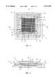
- FIG. 1is perspective view of a figure in a scene being focused by a lens onto the sensor array of a solid state sensor array package that is mounted to and in optical alignment with the lens in accordance with the method and apparatus of the present invention
- FIG. 2is a top plan view of an optical sensor array package of one type that is contemplated by the present invention
- FIG. 3is a cross-sectional elevation view of the sensor package shown in FIG. 2, as revealed by the section taken along the line III--III therein;
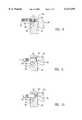
- FIG. 4is a side elevation view of an optical pattern recognition apparatus scanning an optical sensor package to locate the absolute positions of its plane, center, and horizontal and vertical axes in accordance with the present invention
- FIG. 5is a side elevation view of mounting recesses being milled into the window of the sensor package of FIG. 4 using computer-controlled milling apparatus;
- FIG. 6is side elevation view of an optical sensor package mounted to and in optical alignment with a lens in accordance with one embodiment of the present invention
- FIG. 7is a side elevation view of an optical sensor package mounted to and in optical alignment with a lens in accordance with another embodiment of the present invention.
- FIGS. 8-10are enlarged, side elevation views of various embodiments of the complementary mounting projections and recesses of the present invention.
- FIG. 1is a perspective view of a two-dimensional scene 1 containing an element 2 being focused by a lens 3 of a camera 4 onto the sensor array 10 of an optical sensor package 5, wherein the sensor package 5 is mounted to and in optical alignment with the lens 3 in accordance with the method and apparatus of the present invention.
- the image-forming element 3is shown schematically as a simple, refracting lens 3.
- the image-forming devicemight comprise a "pin-hole” lens, or an elongated slit of the type found in the gate of some film or bar-code scanners. Accordingly, although a simple, single-element lens 3 is shown and described throughout the description herein, it should be understood this invention is not limited to this particular type of image-forming element.
- the particular sensor package 5 shown in FIG. 1is a ball grid array (“BGA”) type of optical sensor package sold commercially under the name, Visionpak,TM but it should also be understood that the present invention is not limited to this particular type of package, but has application to other types of sensor packages as well, such as through-pin grid array (“PGA”) packages, or conventional quad-flat (“QFP”) packages, and other types that are known in the art.
- BGAball grid array
- PGAthrough-pin grid array
- QFPquad-flat
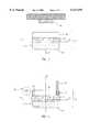
- the sensor package 5is shown in a top plan view in FIG. 2 and in cross-section in FIG. 3, as revealed by the section taken along the lines III--III in FIG. 2.
- the package 5comprises an insulative substrate 6 having a semiconductor chip 8 attached to its upper surface, typically by an epoxy adhesive.
- the substrate 6may be made of a ceramic material, e.g., silicon dioxide, a metal, e.g., Kovar, or a composite, e.g., resin and fiberglass.
- the semiconductor chip 8has a two-dimensional, rectangular sensor array 10 comprising a large number of photo sensors formed in it that are each capable of converting the light incident upon it into an electrical signal that is proportional to the intensity, and in the case of a color camera or the like, the color and hue of the incident light.
- the individual photo sensorsmay be, among others, CCDs or CMOS devices that are formed by photolithography techniques that are known in the art.
- Signal processing circuitry(not illustrated) is typically provided external to the sensor for converting the signals generated by the photo sensors into, typically, a digital signal capable of being stored, processed, or distributed as a "pixel,” or small, rectangular element, of the imaged scene 1.
- the sensor array 10lies in a plane 12 corresponding to the top surface of the chip 8 (see FIG. 3) and has an optical center 14 located at the geometric center of the array. It should be noted that, while the center 14 of the sensor array 10 is shown coincident with the centers of both the underlying chip 8 and the substrate 6, it may be that, in some cases, the center 14 of the array will be offset from the centers of the chip 8 and/or the substrate 6. This is because it may be desirable in some applications to include additional, space-occupying circuitry on the chip 8 itself, and/or an additional chip on the substrate 6 that is dedicated to, e.g., signal processing, sampling, or rastering functions, and the like.
- the sensor array 10may further be thought to have associated with it a set of three orthogonal axes that intersect at the center 14 of the array: a horizontal axis H, a vertical axis V, both of which lie in the plane 12 of the array, and a Z axis that is orthogonal to that plane.
- the upper surface of the substrate 6 of the sensor package 5typically includes a plurality of conductive traces (not illustrated) to which the circuitry of the array 10 is electrically connected by a plurality of fine conductive wires 16 that are bonded at opposite ends to pads on the upper surface of the chip 8 and to pads on the upper surface of the substrate 6, respectively.
- the wires 16carry electrical power and signals between the sensor array 10 and the ambient circuitry (not illustrated), and to this effect, the substrate 6 of the package typically includes a plurality of conductive, plated-through "via" holes (not illustrated) to convey the power and signals to the bottom surface of the substrate 6, where, in a BGA package, they in turn connect to a plurality of solder balls 18 formed on the bottom surface of the substrate 6.
- the solder balls 18function as electrical input/output terminals of the sensor package 5, and also, to mount and connect the sensor package 5 to, e.g., an associated power and control PCB 20, such as shown in FIGS. 3, 6 and 7.
- the chip 8After the chip 8 has been mounted and electrically connected to the substrate 6, it is desirable to protect the delicate circuitry of the sensor array 10 and the bonded wires 16 from harmful environmental elements, such as moisture, yet permit image light incident on the package to reach the underlying sensor array 10 unchanged in its optical properties.
- Thisis achieved in the exemplary optical BGA package illustrated by enclosing the chip 8 and the bonded wires 16 within a sealed chamber 22 defined by side walls 24, comprising a strong epoxy resin, and a transparent lid, or window 26, mounted on the top surface of the side walls 24.
- the chamber 22is created by running a continuous bead 24 of a fairly viscous epoxy resin around the margin of the upper surface of the substrate 6 outside of the chip 8 and the connection wires 16, and then placing the transparent window 26 in contact with the top surface of the bead and maintaining it there while the epoxy bead is cured, thereby attaching the window 26 permanently to the substrate above the chip 8.
- the window 26may be made of glass, quartz, diamond, sapphire, or a clear, hard plastic, such as an acrylic. In some applications, it may be desirable to evacuate the chamber 22, whereas, in others, it may be desirable to fill the chamber 22 with a special-purpose gas, such as dry Nitrogen, Argon or the like, depending on the particular application.
- a conventional refractive lens 3 of a camera 4will focus light reflected or emitted by an element 2 of a two-dimensional scene 1 onto a focal plane (not illustrated) that is orthogonal to the optical axis Z of the lens 3 and located a specific distance (viz., the "focal length" of the lens) behind the lens.
- the element 2 in the scene 1may be thought to lie in a plane that is defined by two orthogonal axes, a horizontal axes H and a vertical axis V that intersect at the center of the scene, and to be orthogonal to a third, intersecting axis Z perpendicular to the H and V axes.
- the sensor array 10For the sensor array 10 to accurately sense the image of the element 2 in the scene 1 imaged by the lens 3, the sensor array must be aligned with the lens such that the plane 12 of the sensor array (see FIGS. 3-7) is coplanar with the focal plane of the lens, or the image will be out of focus. Further, the center 14 of the sensor array 10 must be centered on, or coincident with, the optical axis Z of the lens, or the image will be off center or only partially sensed. And finally, the horizontal and vertical axes H and V of the rectangular array 10 must be aligned with the horizontal and vertical axes H and V of the scene imaged by the lens 3, or the image sensed will be canted relative to the original scene.
- the task of optically aligning the sensor array 10 with the lens 3involves controlling the position of the array relative to the lens in six directions of movement, three linear, viz., along the X, Y, and Z axes of the array, and three angular, or rotational, viz., ⁇ X , ⁇ Y , and ⁇ Z , about those three respective axes.
- the two methods employed by the prior art to deal with this alignment taskare described in detail above, namely the "custom" alignment method, and the "blind” alignment method.
- the blind methodincurs a substantial buildup of tolerances between the sensor array 10 and the lens 3 to which it is aligned, and typically necessitates holding relatively small, or precise, relative tolerances in the mounting of the chip 8 to the substrate 6, the mounting of the sensor package 5 to the underlying sensor electronics PCB 20, and the mounting of the PCB 20 to the lens 3.
- the followingis a description of how the present invention eliminates, or "bypasses,” much of this tolerance buildup.
- a fixture for mounting the package 5 of the sensor array 20 on the lens 3is formed on, or attached to, the lens.
- the fixturecomprises a plurality of mounting features 30 for engaging the package of the sensor array at predetermined positions measured relative to the focal plane of the lens, the optical axis Z of the lens, and the horizontal and vertical axes H and V of the scene 1 imaged by the lens.
- the mounting fixturecomprises a plurality of standoffs, or projections 30, preferably at least three in number, that are arrayed around the optical axis Z of the lens 3 at distinct, predetermined polar coordinates measured relative to that axis and the horizontal and vertical axes of the scene 1 imaged by the lens 3.
- the projections 30have distal ends 32 that extend toward the focal plane of the lens in a direction parallel to its optical axis Z, and include two mechanical features, which are described below, that are used to optically align the sensor array 10 with the lens 3.
- the first of these features 34is either a planar element 34 located at the very distal end 32 of each projections 30, or the frustrum 34 of a cone.
- the first feature 34consists of a small, planar, circular or polygonal element, depending on the cross-sectional shape of the projection, as illustrated in FIGS. 8 and 9.
- the first alignment feature 34is the frustum of a cone.
- first alignment features 34will define a plane that is parallel to the focal plane of the lens 3. Further, if these first features 34 are engaged with corresponding, complementary alignment features in the sensor package 5 that are appropriately located relative to the plane 12 of the sensor array 10, then the plane 12 of the sensor array 10 will be positioned such that it is coplanar with the focal plane of the lens 3.
- the second feature 36 of the distal ends 32 of the projections 30 used in the present invention to optically align the sensor array 10 with the lens 3comprises the outer surfaces of the distal ends 32 of the projections 30 that contact the sensor package 5 (See FIGS. 8-10).
- these second alignment features 36are each located at a predetermined radial distance from the optical axis Z of the lens 3.
- these second features 36are engaged with corresponding, complementary features in the sensor package 5 that are located at identical radial distances relative to the center 14 of the sensor array 10, then the center 14 of the sensor array 10 will be positioned such that it is coincident with the optical axis Z of the lens 3.
- these second alignment features 36 of the distal ends 32 of the projections 30it will be seen that they are each oriented at a predetermined angular orientation relative to the horizontal and vertical axes H and V of a scene 1 imaged by the lens 3. Therefore, if these second features 36 are engaged with corresponding, complementary features in the sensor package 5 that are located at identical, corresponding angular orientations relative to the horizontal and vertical axes H and V of the sensor array 10, then the horizontal and vertical axes H and V of the sensor array 10 will be positioned such that they are aligned with the horizontal and vertical axes H and V, respectively, of a scene 1 imaged by the lens 3.
- the projections 30may be formed as an integral fixture that mounts to the lens 3, e.g., a bezel or other support for the lens, such as the configuration illustrated in FIG. 1.
- the projections 30may be individually constructed and attached to the lens 3, one at a time.
- the projectionscan be integrally and simultaneously formed on a body supporting the lens 3, such as a cast or molded camera or scanner body.
- the prior artrelies on a "dead-reckoning" method, in which the sensor array 10 is located relative to two orthogonal edges of the chip 8, which in turn, is typically positioned relative to the substrate 6 by bringing those two orthogonal edges of the chip into contact with mechanical features, such as ledges or pins, located on the substrate.
- mechanical featuressuch as ledges or pins, located on the substrate.
- the method of the present inventionbypasses the above "relative position" tolerance buildup by first packaging the chip 8 in the sensor package 5, then locating the absolute positions of the essential sensor array optical features independent of any mechanical features on the package, the substrate 6, or the sensor-mounting PCB 20 using automated pattern recognition equipment, and then forming the corresponding, complementary mounting features in the sensor package 5 relative to those absolute locations.
- Thisis illustrated schematically in FIG. 4, where an optical pattern recognition camera 40 is shown scanning the top surface of the sensor chip 8 through the clear window 26 of the fully assembled sensor package 5 to find the absolute locations of the plane 12, the center 14, and the horizontal and vertical axes H and V of the sensor array 10 inside of the package.
- automated pattern recognition equipmentis already in fairly wide use throughout the semiconductor manufacturing industry for such purposes as, for example, wafer sawing, "pick-and-place" attachment of dies and other component, wire bonding, and the like.
- the pattern recognition apparatuslocates the optical features of the sensor array 10 by focusing directly on the features of the array itself, which is visible through the transparent window 26.
- These locating targets 41can be formed with great precision relative to the sensor array 10 concurrently with its formation using, e.g., the same photolithography techniques used to form the array itself.
- the pattern recognition apparatus 40is then ready to scan the next package 5, while the previously-scanned package moves on to a milling station for formation of the corresponding, complementary mounting features in the package.
- the pattern recognition scanning apparatus 40can be mounted on a head that is moved away from the scanned package to permit a movable milling head to move into position above the package to form the complementary mounting features, all or any part of which processes can be automatically controlled by a computer.
- the next stageinvolves forming the corresponding, complementary mounting features 42 in the package 5 of the sensor array 10 at positions measured relative to the absolute locations of the sensor array 10 features found by the pattern recognition equipment 40 above.
- these featurescomprise recesses 42 formed at positions corresponding to the predetermined positions of the projections 30 on the lens 3 described above, as measured relative to the focal plane and the optical axis Z of the lens 3, and the horizontal and vertical axes H and V of a scene 1 imaged by the lens 3, respectively.
- the recesses 42are preferably milled into the package 5 of the sensor array 10 at their respective polar coordinate positions and to their respective depths using computer-controlled milling apparatus 44, 46 that is positioned in accordance with the absolute sensor array feature location data determined and supplied to the milling apparatus by the automated optical pattern recognition apparatus 40 described above, combined with the pre-programmed, predetermined positional information relating to the projections 30.
- the recesses 42may comprise either a cylindrical bore 42', milled by a cylindrical boring tool 44, or an open-sided slot 42", milled by a wheel cutter 46, either of which is located at a margin of the clear window 26 of the sensor package 5 (see FIGS. 5 and 8-10).
- the recesses 42regardless of their type, include first and second mechanical alignment features 34' and 36' that complement respective ones of the first and second mechanical alignment feature 34 and 36 on the distal ends 32 of the projections 30 described above.
- each of the recesses 32comprises a flat "floor" 34, in the case of either a cylindrical bore 42', or a semicircular, rectangular, or V-shaped slot 42", as illustrated in FIGS. 8 and 9, or the frustum 34' of a cone, in the case of a conical bore, as illustrated in FIG. 10, that complements the first distal end feature 34 on the distal ends 32 of the projections 30.
- these first recess featurescan be made to lie in a plane that is parallel to the plane of the sensor array and spaced slightly above it, such that, when these first recess alignment features 34' are abutted against their corresponding first distal end alignment features 34 on the projections 30, the plane 12 of the sensor array 10 will be positioned coplanar with the focal plane of the lens 3.
- the recesses 42contain second mechanical alignment features 36' complementary to the second mechanical alignment features 36 located on the distal ends 32 of the projections 30, namely, the inner wall surfaces of the recesses 42.
- the second recess features 36'are milled at the appropriate radial distances relative to the absolute location of the center 14 of the sensor array 10, and at appropriate angular positions relative to the absolute angular locations of the horizontal and vertical axes H and Z of the array 10, respectively, then when corresponding pairs of the second distal end alignment features 36 and the second recess alignment features 36' are engaged with each other, the center 14 of the sensor array 10 will be positioned coincidentally with the optical axis Z of the lens 3, and the horizontal and vertical axes H and V of the sensor array 10 will be aligned with the horizontal and vertical axes H and V of a scene 1 imaged by the lens 3, respectively.
- the method and apparatus of the present inventionmake it possible to fabricate cameras 4 (or other imaging devices), and sensor array packages 5 on separate lines and to assemble them interchangeably with each other, in precise optical alignment, in a simple, low-cost, high-volume operation. That operation is illustrated schematically in FIG. 6, in which the recesses comprise cylindrical bores 42', and in FIG. 7, in which the recesses comprise slots 42", both types milled into the margins of the transparent window 26.
- Permanent mounting of the sensor package 5 to and in optical alignment with the lens 3can be achieved, for example, by simply applying a small amount of a suitable adhesive, e.g., cyanoacrylate, onto the distal ends 32 of the projections 30, then pressing the package 5 onto the projections 30 such that the distal ends 32 of the projections 30 engage and bottom out in the corresponding recesses 32, and holding the package 5 in that position until the adhesive cures.
- a suitable adhesivee.g., cyanoacrylate
- One way to achieve thisis to color-code at least one of the distal ends 32 of the projections 30 and its corresponding recess 42 such that their specific correspondence is visually apparent.
- a methodis not fail-safe.
- Another, fail-safe way to prevent the problemis to position corresponding pairs of projections 30 and recesses 42 in a pattern that is radially asymmetrical, or at best, only bilaterally symmetrical, about the Z axis of the lens 3, such that the sensor package 5 can be assembled to the lens 3 in only one relative orientation.
- a third, fail-safe methodis to "key" one pair of corresponding distal ends 32 and recesses 42 to each other, such as by providing them with a different cross-sectional shape than the other pairs, so that they can engage only with each other and with none of the other mounting features.
- annular sleevemounted coaxially on the lens 3 for the plurality of projections 30 thereon, and to mill an annular shoulder, or rabbet, into the face of the round window around its periphery, in place of the plurality of recesses milled into the margins of the rectangular window.
- the plane of the sensorwill be coplanar with the focal plane of the lens, and the sensor array will be centered on its optical axis.
- the recesses 42are milled into the window 26 of the sensor package 5.
- the substratecan then be deemed an integral part of the sensor array "package," and in such an embodiment, the substrate 20 can be provided with an appropriate number of oversized standoffs located outboard of the sensor package 5 into which the recesses 42 are milled.
Landscapes
- Transforming Light Signals Into Electric Signals (AREA)
- Solid State Image Pick-Up Elements (AREA)
Abstract
Description
Claims (34)
Priority Applications (1)
| Application Number | Priority Date | Filing Date | Title |
|---|---|---|---|
| US09/422,008US6117193A (en) | 1999-10-20 | 1999-10-20 | Optical sensor array mounting and alignment |
Applications Claiming Priority (1)
| Application Number | Priority Date | Filing Date | Title |
|---|---|---|---|
| US09/422,008US6117193A (en) | 1999-10-20 | 1999-10-20 | Optical sensor array mounting and alignment |
Publications (1)
| Publication Number | Publication Date |
|---|---|
| US6117193Atrue US6117193A (en) | 2000-09-12 |
Family
ID=23673007
Family Applications (1)
| Application Number | Title | Priority Date | Filing Date |
|---|---|---|---|
| US09/422,008Expired - LifetimeUS6117193A (en) | 1999-10-20 | 1999-10-20 | Optical sensor array mounting and alignment |
Country Status (1)
| Country | Link |
|---|---|
| US (1) | US6117193A (en) |
Cited By (52)
| Publication number | Priority date | Publication date | Assignee | Title |
|---|---|---|---|---|
| US6359652B1 (en)* | 1997-02-20 | 2002-03-19 | Matsushita Electric Industrial Co., Ltd. | Mounting structure for the photographic element of a camera |
| FR2822326A1 (en)* | 2001-03-16 | 2002-09-20 | Atmel Grenoble Sa | LOW COST ELECTRONIC CAMERA IN INTEGRATED CIRCUIT TECHNOLOGY |
| US6480682B1 (en)* | 1999-09-03 | 2002-11-12 | Fuji Photo Film Co., Ltd. | Photometric device comprising a photo sensor mounted on a circuit board |
| US20030143781A1 (en)* | 2002-01-31 | 2003-07-31 | Mclellan Neil Robert | Encapsulated integrated circuit package and method of manufacturing an integrated circuit package |
| FR2835654A1 (en)* | 2002-02-06 | 2003-08-08 | St Microelectronics Sa | OPTICAL SEMICONDUCTOR PACKAGE WITH COUPLED LENS HOLDER |
| FR2835653A1 (en)* | 2002-02-06 | 2003-08-08 | St Microelectronics Sa | Optical semiconductor device, has IC chip casing enclosing optical sensors |
| EP1357606A1 (en)* | 2002-04-22 | 2003-10-29 | Scientek Corporation | Image sensor semiconductor package |
| EP1357605A1 (en)* | 2002-04-22 | 2003-10-29 | Scientek Corporation | Image sensor semiconductor package with castellation |
| US6661084B1 (en)* | 2000-05-16 | 2003-12-09 | Sandia Corporation | Single level microelectronic device package with an integral window |
| US20030232461A1 (en)* | 2002-06-04 | 2003-12-18 | Bolken Todd O. | Methods for packaging image sensitive electronic devices |
| US20030234454A1 (en)* | 2002-06-24 | 2003-12-25 | Serafin Pedron | Integrated circuit package and method of manufacturing the integrated circuit package |
| US6674159B1 (en)* | 2000-05-16 | 2004-01-06 | Sandia National Laboratories | Bi-level microelectronic device package with an integral window |
| US6695493B2 (en) | 2000-10-06 | 2004-02-24 | Bae Systems Information And Electronic Systems Integration Inc | Optical fiber utilization for VCSEL driven communications |
| US6710945B1 (en) | 2002-06-03 | 2004-03-23 | Amkor Technology, Inc. | Injection molded lens-barrel assembly and method for fabricating lens-barrel and mount assemblies |
| US6734552B2 (en) | 2001-07-11 | 2004-05-11 | Asat Limited | Enhanced thermal dissipation integrated circuit package |
| US20040125701A1 (en)* | 2001-03-30 | 2004-07-01 | Louis Raillon | Towed low-frequency underwater detection system |
| US20040207926A1 (en)* | 2002-02-22 | 2004-10-21 | Buckman Lisa A. | Structure and apparatus for a very short haul, free space, and fiber optic interconnect and data link |
| US20040252195A1 (en)* | 2003-06-13 | 2004-12-16 | Jih-Yung Lu | Method of aligning lens and sensor of camera |
| US6861720B1 (en) | 2001-08-29 | 2005-03-01 | Amkor Technology, Inc. | Placement template and method for placing optical dies |
| US6873024B1 (en) | 2002-05-15 | 2005-03-29 | Eastman Kodak Company | Apparatus and method for wafer level packaging of optical imaging semiconductor devices |
| FR2860644A1 (en)* | 2003-10-06 | 2005-04-08 | St Microelectronics Sa | COMPONENT, PLATE AND SEMICONDUCTOR HOUSING WITH OPTICAL SENSOR |
| US20050248680A1 (en)* | 2004-05-04 | 2005-11-10 | Tessera, Inc. | Compact lens turret assembly |
| EP1619726A1 (en)* | 2004-07-22 | 2006-01-25 | St Microelectronics S.A. | Package for optical semiconductor detector |
| US20060043461A1 (en)* | 2002-11-20 | 2006-03-02 | Stmicroelectronics S.R.L. | Process for manufacturing a byte selection transistor for a matrix of non volatile memory cells and corresponding structure |
| US7015072B2 (en) | 2001-07-11 | 2006-03-21 | Asat Limited | Method of manufacturing an enhanced thermal dissipation integrated circuit package |
| US20060109366A1 (en)* | 2004-05-04 | 2006-05-25 | Tessera, Inc. | Compact lens turret assembly |
| US20060108518A1 (en)* | 2004-11-15 | 2006-05-25 | Nsmc Holdings International Corp. Ltd. | Structure for calibrating packaging of electric micro-optic modules |
| US20070058159A1 (en)* | 2003-11-14 | 2007-03-15 | Koninklijke Philips Electronics N.V. | Method of and apparatus for determining focus of an imaging system |
| US7205095B1 (en) | 2003-09-17 | 2007-04-17 | National Semiconductor Corporation | Apparatus and method for packaging image sensing semiconductor chips |
| EP1796168A2 (en) | 2005-12-12 | 2007-06-13 | Robert Bosch Gmbh | Optical module and mounting method thereof |
| US20070255522A1 (en)* | 2004-10-29 | 2007-11-01 | Honeywell International, Inc. | Method for verifying sensors installation and determining the location of the sensors after installation in a structural health management system |
| US20100164081A1 (en)* | 2008-12-29 | 2010-07-01 | Texas Instruments Incorporated | Micro-Optical Device Packaging System |
| US20100236063A1 (en)* | 2008-02-13 | 2010-09-23 | Panasonic Corporation | Imaging device, and method for manufacturing the same |
| WO2013053908A1 (en)* | 2011-10-14 | 2013-04-18 | Häcker Automation GmbH | Production device and method for manufacturing microelectronic products |
| CN103297799A (en)* | 2012-02-23 | 2013-09-11 | 苹果公司 | Testing an optical characteristic of a camera component |
| US8542451B2 (en) | 2009-03-25 | 2013-09-24 | Magna Electronics Inc. | Vehicular camera and lens assembly |
| US8553131B2 (en) | 2010-06-03 | 2013-10-08 | Bendix Commercial Vehicle Systems Llc | Six-axis mount |
| US8786713B1 (en)* | 2013-03-14 | 2014-07-22 | Automation Engineering, Inc. | Fixture for aligning auto-focus lens assembly to camera sensor |
| US9451138B2 (en) | 2013-11-07 | 2016-09-20 | Magna Electronics Inc. | Camera for vehicle vision system |
| US9749509B2 (en) | 2014-03-13 | 2017-08-29 | Magna Electronics Inc. | Camera with lens for vehicle vision system |
| EP1787337B1 (en)* | 2004-08-23 | 2018-03-14 | OSRAM Opto Semiconductors GmbH | Module with an optoelectronic component and a device |
| US10142532B2 (en) | 2016-04-08 | 2018-11-27 | Magna Electronics Inc. | Camera for vehicle vision system |
| US10230875B2 (en) | 2016-04-14 | 2019-03-12 | Magna Electronics Inc. | Camera for vehicle vision system |
| US10237456B2 (en) | 2016-08-22 | 2019-03-19 | Magna Electronics Inc. | Vehicle camera assembly process |
| US10250004B2 (en) | 2015-11-05 | 2019-04-02 | Magna Electronics Inc. | Method of forming a connector for an electrical cable for electrically connecting to a camera of a vehicle |
| US10351072B2 (en) | 2015-11-05 | 2019-07-16 | Magna Electronics Inc. | Vehicle camera with modular construction |
| US10462375B2 (en) | 2011-08-02 | 2019-10-29 | Magna Electronics Inc. | Exterior viewing camera module for vehicle vision system |
| US10523853B2 (en) | 2008-10-16 | 2019-12-31 | Magna Electronics Inc. | Method of assembling camera for vehicular applications |
| US10560613B2 (en) | 2015-11-05 | 2020-02-11 | Magna Electronics Inc. | Vehicle camera with modular construction |
| US10576909B2 (en) | 2011-04-20 | 2020-03-03 | Magna Electronics Inc. | Vehicular vision system with windshield mounted camera |
| US10787125B2 (en) | 2011-08-02 | 2020-09-29 | Magna Electronics Inc. | Vehicular camera system |
| US12328491B1 (en) | 2009-03-25 | 2025-06-10 | Magna Electronics Inc. | Vehicular camera and lens assembly |
Citations (8)
| Publication number | Priority date | Publication date | Assignee | Title |
|---|---|---|---|---|
| US4318135A (en)* | 1979-10-12 | 1982-03-02 | Xerox Corporation | Alignment system for scanning arrays |
| US4457017A (en)* | 1980-06-11 | 1984-06-26 | Hitachi, Ltd. | Method of adjusting position of solid-state scanning element and mounting same |
| US4591901A (en)* | 1984-03-30 | 1986-05-27 | Rca Corporation | Television camera with solid-state imagers mounted to a prism |
| US4594613A (en)* | 1982-02-16 | 1986-06-10 | Canon Kabushiki Kaisha | Solid-state imaging device assembly |
| US4803557A (en)* | 1988-01-11 | 1989-02-07 | Eastman Kodak Company | Adjustable mount for image sensor |
| US5267043A (en)* | 1991-08-26 | 1993-11-30 | Eastman Kodak Company | Film gate apparatus for a virtual contact color film scanner |
| US5559556A (en)* | 1992-06-30 | 1996-09-24 | Icl Systems Ab | Apparatus for connecting an image sensor and an optical unit to a circuit board so that they are properly aligned |
| US5828409A (en)* | 1995-06-30 | 1998-10-27 | Eastman Kodak Company | Film scanner mount assembly for a solid state sensor |
- 1999
- 1999-10-20USUS09/422,008patent/US6117193A/ennot_activeExpired - Lifetime
Patent Citations (8)
| Publication number | Priority date | Publication date | Assignee | Title |
|---|---|---|---|---|
| US4318135A (en)* | 1979-10-12 | 1982-03-02 | Xerox Corporation | Alignment system for scanning arrays |
| US4457017A (en)* | 1980-06-11 | 1984-06-26 | Hitachi, Ltd. | Method of adjusting position of solid-state scanning element and mounting same |
| US4594613A (en)* | 1982-02-16 | 1986-06-10 | Canon Kabushiki Kaisha | Solid-state imaging device assembly |
| US4591901A (en)* | 1984-03-30 | 1986-05-27 | Rca Corporation | Television camera with solid-state imagers mounted to a prism |
| US4803557A (en)* | 1988-01-11 | 1989-02-07 | Eastman Kodak Company | Adjustable mount for image sensor |
| US5267043A (en)* | 1991-08-26 | 1993-11-30 | Eastman Kodak Company | Film gate apparatus for a virtual contact color film scanner |
| US5559556A (en)* | 1992-06-30 | 1996-09-24 | Icl Systems Ab | Apparatus for connecting an image sensor and an optical unit to a circuit board so that they are properly aligned |
| US5828409A (en)* | 1995-06-30 | 1998-10-27 | Eastman Kodak Company | Film scanner mount assembly for a solid state sensor |
Cited By (130)
| Publication number | Priority date | Publication date | Assignee | Title |
|---|---|---|---|---|
| US6359652B1 (en)* | 1997-02-20 | 2002-03-19 | Matsushita Electric Industrial Co., Ltd. | Mounting structure for the photographic element of a camera |
| US6480682B1 (en)* | 1999-09-03 | 2002-11-12 | Fuji Photo Film Co., Ltd. | Photometric device comprising a photo sensor mounted on a circuit board |
| US6661084B1 (en)* | 2000-05-16 | 2003-12-09 | Sandia Corporation | Single level microelectronic device package with an integral window |
| US6674159B1 (en)* | 2000-05-16 | 2004-01-06 | Sandia National Laboratories | Bi-level microelectronic device package with an integral window |
| US6695493B2 (en) | 2000-10-06 | 2004-02-24 | Bae Systems Information And Electronic Systems Integration Inc | Optical fiber utilization for VCSEL driven communications |
| FR2822326A1 (en)* | 2001-03-16 | 2002-09-20 | Atmel Grenoble Sa | LOW COST ELECTRONIC CAMERA IN INTEGRATED CIRCUIT TECHNOLOGY |
| WO2002075815A1 (en)* | 2001-03-16 | 2002-09-26 | Atmel Grenoble S.A. | Low cost electronic camera made with integrated circuit technology |
| US20040080658A1 (en)* | 2001-03-16 | 2004-04-29 | Pierre Cambou | Low cost electronic camera made using integrated circuit technology |
| US20040125701A1 (en)* | 2001-03-30 | 2004-07-01 | Louis Raillon | Towed low-frequency underwater detection system |
| US6901029B2 (en) | 2001-03-30 | 2005-05-31 | Thales | Towed low-frequency underwater detection system |
| US6734552B2 (en) | 2001-07-11 | 2004-05-11 | Asat Limited | Enhanced thermal dissipation integrated circuit package |
| US7015072B2 (en) | 2001-07-11 | 2006-03-21 | Asat Limited | Method of manufacturing an enhanced thermal dissipation integrated circuit package |
| US6861720B1 (en) | 2001-08-29 | 2005-03-01 | Amkor Technology, Inc. | Placement template and method for placing optical dies |
| US20050077613A1 (en)* | 2002-01-31 | 2005-04-14 | Mclellan Neil Robert | Integrated circuit package |
| US20030143781A1 (en)* | 2002-01-31 | 2003-07-31 | Mclellan Neil Robert | Encapsulated integrated circuit package and method of manufacturing an integrated circuit package |
| US6790710B2 (en) | 2002-01-31 | 2004-09-14 | Asat Limited | Method of manufacturing an integrated circuit package |
| FR2835654A1 (en)* | 2002-02-06 | 2003-08-08 | St Microelectronics Sa | OPTICAL SEMICONDUCTOR PACKAGE WITH COUPLED LENS HOLDER |
| FR2835653A1 (en)* | 2002-02-06 | 2003-08-08 | St Microelectronics Sa | Optical semiconductor device, has IC chip casing enclosing optical sensors |
| US20040065952A1 (en)* | 2002-02-06 | 2004-04-08 | Christophe Prior | Optical semiconductor device and method of manufacture |
| US6972497B2 (en) | 2002-02-06 | 2005-12-06 | Stmicroelectronics S.A. | Optical semiconductor device and method of manufacture |
| US20040207926A1 (en)* | 2002-02-22 | 2004-10-21 | Buckman Lisa A. | Structure and apparatus for a very short haul, free space, and fiber optic interconnect and data link |
| US7978981B2 (en)* | 2002-02-22 | 2011-07-12 | Avago Technologies Fiber Ip (Singapore) Pte. Ltd. | Structure and apparatus for a very short haul, free space, and fiber optic interconnect and data link |
| EP1357605A1 (en)* | 2002-04-22 | 2003-10-29 | Scientek Corporation | Image sensor semiconductor package with castellation |
| EP1357606A1 (en)* | 2002-04-22 | 2003-10-29 | Scientek Corporation | Image sensor semiconductor package |
| US6873024B1 (en) | 2002-05-15 | 2005-03-29 | Eastman Kodak Company | Apparatus and method for wafer level packaging of optical imaging semiconductor devices |
| US6710945B1 (en) | 2002-06-03 | 2004-03-23 | Amkor Technology, Inc. | Injection molded lens-barrel assembly and method for fabricating lens-barrel and mount assemblies |
| US20030232461A1 (en)* | 2002-06-04 | 2003-12-18 | Bolken Todd O. | Methods for packaging image sensitive electronic devices |
| US20060267169A1 (en)* | 2002-06-04 | 2006-11-30 | Bolken Todd O | Image sensitive electronic device packages |
| US20050116355A1 (en)* | 2002-06-04 | 2005-06-02 | Bolken Todd O. | Packages for image sensitive electronic devices |
| US6906403B2 (en) | 2002-06-04 | 2005-06-14 | Micron Technology, Inc. | Sealed electronic device packages with transparent coverings |
| US7195940B2 (en) | 2002-06-04 | 2007-03-27 | Micron Technology, Inc. | Methods for packaging image sensitive electronic devices |
| US7553688B2 (en) | 2002-06-04 | 2009-06-30 | Micron Technology, Inc. | Methods for packaging image sensitive electronic devices |
| US20060051892A1 (en)* | 2002-06-04 | 2006-03-09 | Bolken Todd O | Methods for packaging image sensitive electronic devices |
| US7419854B2 (en) | 2002-06-04 | 2008-09-02 | Micron Technology, Inc. | Methods for packaging image sensitive electronic devices |
| US7387902B2 (en) | 2002-06-04 | 2008-06-17 | Micron Technology, Inc. | Methods for packaging image sensitive electronic devices |
| US20060051891A1 (en)* | 2002-06-04 | 2006-03-09 | Bolken Todd O | Methods for packaging image sensitive electronic devices |
| US20060046351A1 (en)* | 2002-06-04 | 2006-03-02 | Bolken Todd O | Methods for packaging image sensitive electronic devices |
| US20030234454A1 (en)* | 2002-06-24 | 2003-12-25 | Serafin Pedron | Integrated circuit package and method of manufacturing the integrated circuit package |
| US6940154B2 (en) | 2002-06-24 | 2005-09-06 | Asat Limited | Integrated circuit package and method of manufacturing the integrated circuit package |
| US20060043461A1 (en)* | 2002-11-20 | 2006-03-02 | Stmicroelectronics S.R.L. | Process for manufacturing a byte selection transistor for a matrix of non volatile memory cells and corresponding structure |
| US20040252195A1 (en)* | 2003-06-13 | 2004-12-16 | Jih-Yung Lu | Method of aligning lens and sensor of camera |
| US7071966B2 (en)* | 2003-06-13 | 2006-07-04 | Benq Corporation | Method of aligning lens and sensor of camera |
| US7205095B1 (en) | 2003-09-17 | 2007-04-17 | National Semiconductor Corporation | Apparatus and method for packaging image sensing semiconductor chips |
| FR2860644A1 (en)* | 2003-10-06 | 2005-04-08 | St Microelectronics Sa | COMPONENT, PLATE AND SEMICONDUCTOR HOUSING WITH OPTICAL SENSOR |
| US20050103987A1 (en)* | 2003-10-06 | 2005-05-19 | Stmicroelectronics S.A. | Semiconductor component, wafer and package having an optical sensor |
| US20070058159A1 (en)* | 2003-11-14 | 2007-03-15 | Koninklijke Philips Electronics N.V. | Method of and apparatus for determining focus of an imaging system |
| US7453581B2 (en)* | 2003-11-14 | 2008-11-18 | Koninklijke Philips Electronics N.V. | Method of and apparatus for determining focus of an imaging system |
| US20100242269A1 (en)* | 2004-05-04 | 2010-09-30 | Tessera, Inc. | Compact lens turret assembly |
| US20060109366A1 (en)* | 2004-05-04 | 2006-05-25 | Tessera, Inc. | Compact lens turret assembly |
| US7768574B2 (en)* | 2004-05-04 | 2010-08-03 | Tessera, Inc. | Compact lens turret assembly |
| US20050248680A1 (en)* | 2004-05-04 | 2005-11-10 | Tessera, Inc. | Compact lens turret assembly |
| US20060017127A1 (en)* | 2004-07-22 | 2006-01-26 | Stmicroelectronics, S.A. | Optical package for a semiconductor sensor |
| EP1619726A1 (en)* | 2004-07-22 | 2006-01-25 | St Microelectronics S.A. | Package for optical semiconductor detector |
| EP1787337B1 (en)* | 2004-08-23 | 2018-03-14 | OSRAM Opto Semiconductors GmbH | Module with an optoelectronic component and a device |
| US7660690B2 (en)* | 2004-10-29 | 2010-02-09 | Honeywell International Inc. | Method for verifying sensors installation and determining the location of the sensors after installation in a structural health management system |
| US20070255522A1 (en)* | 2004-10-29 | 2007-11-01 | Honeywell International, Inc. | Method for verifying sensors installation and determining the location of the sensors after installation in a structural health management system |
| US20060108518A1 (en)* | 2004-11-15 | 2006-05-25 | Nsmc Holdings International Corp. Ltd. | Structure for calibrating packaging of electric micro-optic modules |
| EP1796168A2 (en) | 2005-12-12 | 2007-06-13 | Robert Bosch Gmbh | Optical module and mounting method thereof |
| EP1796168A3 (en)* | 2005-12-12 | 2011-01-05 | Robert Bosch Gmbh | Optical module and mounting method thereof |
| US20100236063A1 (en)* | 2008-02-13 | 2010-09-23 | Panasonic Corporation | Imaging device, and method for manufacturing the same |
| US7979982B2 (en)* | 2008-02-13 | 2011-07-19 | Panasonic Corporation | Imaging device, and method for manufacturing the same |
| US10979611B2 (en) | 2008-10-16 | 2021-04-13 | Magna Electronics Inc. | Method of assembling camera for vehicular applications |
| US10523853B2 (en) | 2008-10-16 | 2019-12-31 | Magna Electronics Inc. | Method of assembling camera for vehicular applications |
| US11240415B2 (en) | 2008-10-16 | 2022-02-01 | Magna Electronics Inc. | Vehicular camera with metallic housing |
| US11617021B2 (en) | 2008-10-16 | 2023-03-28 | Magna Electronics Inc. | Vehicular camera module |
| US11785327B2 (en) | 2008-10-16 | 2023-10-10 | Magna Electronics Inc. | Vehicular camera module |
| US12206976B2 (en) | 2008-10-16 | 2025-01-21 | Magna Electronics | Vehicular camera module |
| US7936033B2 (en) | 2008-12-29 | 2011-05-03 | Texas Instruments Incorporated | Micro-optical device packaging system |
| US20110204464A1 (en)* | 2008-12-29 | 2011-08-25 | Texas Instruments Incorporated | Micro-Optical Device Packaging System |
| US8445984B2 (en) | 2008-12-29 | 2013-05-21 | Texas Instruments Incorporated | Micro-optical device packaging system |
| US20100164081A1 (en)* | 2008-12-29 | 2010-07-01 | Texas Instruments Incorporated | Micro-Optical Device Packaging System |
| US9338334B2 (en) | 2009-03-25 | 2016-05-10 | Magna Electronics Inc. | Vehicular camera and lens assembly |
| US11146713B2 (en) | 2009-03-25 | 2021-10-12 | Magna Electronics Inc. | Vehicular camera and lens assembly |
| US10917548B2 (en) | 2009-03-25 | 2021-02-09 | Magna Electronics Inc. | Vehicular camera and lens assembly and method of manufacturing same |
| US10708476B2 (en) | 2009-03-25 | 2020-07-07 | Magna Electronics Inc. | Vehicular camera and lens assembly and method of manufacturing same |
| US12035027B2 (en) | 2009-03-25 | 2024-07-09 | Magna Electronics Inc. | Vehicular camera and lens assembly |
| US9277104B2 (en) | 2009-03-25 | 2016-03-01 | Magna Electronics Inc. | Vehicular camera and lens assembly and method of manufacturing same |
| US12328491B1 (en) | 2009-03-25 | 2025-06-10 | Magna Electronics Inc. | Vehicular camera and lens assembly |
| US10015377B2 (en) | 2009-03-25 | 2018-07-03 | Magna Electronics Inc. | Vehicular camera and lens assembly and method of manufacturing same |
| US8542451B2 (en) | 2009-03-25 | 2013-09-24 | Magna Electronics Inc. | Vehicular camera and lens assembly |
| US11457134B2 (en) | 2009-03-25 | 2022-09-27 | Magna Electronics Inc. | Vehicular camera and lens assembly |
| US10270949B2 (en) | 2009-03-25 | 2019-04-23 | Magna Electronics Inc. | Vehicular camera and lens assembly |
| US8553131B2 (en) | 2010-06-03 | 2013-10-08 | Bendix Commercial Vehicle Systems Llc | Six-axis mount |
| US11052834B2 (en) | 2011-04-20 | 2021-07-06 | Magna Electronics Inc. | Vehicular vision system with windshield mounted camera |
| US10576909B2 (en) | 2011-04-20 | 2020-03-03 | Magna Electronics Inc. | Vehicular vision system with windshield mounted camera |
| US11667252B2 (en) | 2011-04-20 | 2023-06-06 | Magna Electronics Inc. | Vehicular vision system with windshield mounted camera |
| US10793086B2 (en) | 2011-04-20 | 2020-10-06 | Magna Electronics Inc. | Vehicular vision system with windshield mounted camera |
| US11427136B2 (en) | 2011-04-20 | 2022-08-30 | Magna Electronics Inc. | Vehicular vision system with windshield mounted camera |
| US10857953B1 (en) | 2011-04-20 | 2020-12-08 | Magna Electronics Inc. | Vehicular vision system with windshield mounted camera |
| US11975660B2 (en) | 2011-04-20 | 2024-05-07 | Magna Electronics Inc. | Vehicular vision system with windshield mounted camera |
| US12246657B2 (en) | 2011-04-20 | 2025-03-11 | Magna Electronics Inc. | Vehicular vision system with windshield mounted camera |
| US11997392B2 (en) | 2011-08-02 | 2024-05-28 | Magna Electronics Inc. | Vehicular camera module |
| US11212453B2 (en) | 2011-08-02 | 2021-12-28 | Magna Electroncs Inc. | Camera module for vehicular driving assist system |
| US11758274B2 (en) | 2011-08-02 | 2023-09-12 | Magna Electronics Inc. | Vehicular camera module |
| US11718228B2 (en) | 2011-08-02 | 2023-08-08 | Magna Electronics Inc. | Vehicular camera system |
| US10462375B2 (en) | 2011-08-02 | 2019-10-29 | Magna Electronics Inc. | Exterior viewing camera module for vehicle vision system |
| US12109951B2 (en) | 2011-08-02 | 2024-10-08 | Magna Electronics Inc. | Vehicular camera system |
| US12162412B2 (en) | 2011-08-02 | 2024-12-10 | Magna Electronics Inc. | Vehicular camera system |
| US10771708B2 (en) | 2011-08-02 | 2020-09-08 | Magna Electronics Inc. | Exterior viewing camera module for vehicle vision system |
| US10787125B2 (en) | 2011-08-02 | 2020-09-29 | Magna Electronics Inc. | Vehicular camera system |
| US12279045B2 (en) | 2011-08-02 | 2025-04-15 | Magna Electronics Inc. | Vehicular camera module |
| WO2013053908A1 (en)* | 2011-10-14 | 2013-04-18 | Häcker Automation GmbH | Production device and method for manufacturing microelectronic products |
| CN103297799B (en)* | 2012-02-23 | 2015-04-08 | 苹果公司 | Testing an optical characteristic of a camera component |
| CN103297799A (en)* | 2012-02-23 | 2013-09-11 | 苹果公司 | Testing an optical characteristic of a camera component |
| US8786713B1 (en)* | 2013-03-14 | 2014-07-22 | Automation Engineering, Inc. | Fixture for aligning auto-focus lens assembly to camera sensor |
| US9635230B2 (en) | 2013-11-07 | 2017-04-25 | Magna Electronics Inc. | Method of assembling camera for vehicle vision system |
| US12273611B2 (en) | 2013-11-07 | 2025-04-08 | Magna Electronics Inc. | Vehicular camera with adhesively bonded construction |
| US9497368B1 (en) | 2013-11-07 | 2016-11-15 | Magna Electronics Inc. | Method of assembling camera for vehicle vision system |
| US10757305B1 (en) | 2013-11-07 | 2020-08-25 | Magna Electronics Inc. | Vehicular camera with adhesively bonded construction |
| US9883088B2 (en) | 2013-11-07 | 2018-01-30 | Magna Electronics Inc. | Method of assembling camera for vehicle vision system |
| US10419652B2 (en) | 2013-11-07 | 2019-09-17 | Magna Electronics Inc. | Vehicular camera with adhesively bonded construction |
| US11108939B2 (en) | 2013-11-07 | 2021-08-31 | Magna Electronics Inc. | Vehicular camera with adhesively bonded construction |
| US10674053B2 (en) | 2013-11-07 | 2020-06-02 | Magna Electronics Inc. | Vehicular camera with adhesively bonded construction |
| US9451138B2 (en) | 2013-11-07 | 2016-09-20 | Magna Electronics Inc. | Camera for vehicle vision system |
| US11622168B2 (en) | 2013-11-07 | 2023-04-04 | Magna Electronics Inc. | Vehicular camera with adhesively bonded construction |
| US10264168B2 (en) | 2013-11-07 | 2019-04-16 | Magna Electronics Inc. | Method of assembling camera for vehicle vision system |
| US9749509B2 (en) | 2014-03-13 | 2017-08-29 | Magna Electronics Inc. | Camera with lens for vehicle vision system |
| US10351072B2 (en) | 2015-11-05 | 2019-07-16 | Magna Electronics Inc. | Vehicle camera with modular construction |
| US10965846B2 (en) | 2015-11-05 | 2021-03-30 | Magna Electronics Inc. | Method of assembling a camera for vehicular vision system |
| US10250004B2 (en) | 2015-11-05 | 2019-04-02 | Magna Electronics Inc. | Method of forming a connector for an electrical cable for electrically connecting to a camera of a vehicle |
| US11528391B2 (en) | 2015-11-05 | 2022-12-13 | Magna Electronics Inc. | Vehicular camera module |
| US11245819B2 (en) | 2015-11-05 | 2022-02-08 | Magna Electronics Inc. | Vehicular camera module |
| US10477083B2 (en) | 2015-11-05 | 2019-11-12 | Magna Electronics Inc. | Camera for vehicular vision system |
| US10560613B2 (en) | 2015-11-05 | 2020-02-11 | Magna Electronics Inc. | Vehicle camera with modular construction |
| US10604084B2 (en) | 2015-11-05 | 2020-03-31 | Magna Electronics Inc. | Vehicle camera with modular construction |
| US10367984B2 (en) | 2016-04-08 | 2019-07-30 | Magna Electronics Inc. | Method of forming camera module for vehicular vision system |
| US10142532B2 (en) | 2016-04-08 | 2018-11-27 | Magna Electronics Inc. | Camera for vehicle vision system |
| US10694090B2 (en) | 2016-04-08 | 2020-06-23 | Magna Electronics Inc. | Method of forming camera module for vehicular vision system |
| US10230875B2 (en) | 2016-04-14 | 2019-03-12 | Magna Electronics Inc. | Camera for vehicle vision system |
| US10237456B2 (en) | 2016-08-22 | 2019-03-19 | Magna Electronics Inc. | Vehicle camera assembly process |
Similar Documents
| Publication | Publication Date | Title |
|---|---|---|
| US6117193A (en) | Optical sensor array mounting and alignment | |
| CA2801349C (en) | Six-axis mount | |
| US5861654A (en) | Image sensor assembly | |
| US5998878A (en) | Image sensor assembly and packaging method | |
| US20040080658A1 (en) | Low cost electronic camera made using integrated circuit technology | |
| KR100556198B1 (en) | Solid state imaging device, method for producing the same, solid state imaging unit and method for producing the same, and imaging apparatus | |
| US7088397B1 (en) | Image sensor packaging with imaging optics | |
| US6762796B1 (en) | Image pickup module having integrated lens and semiconductor chip | |
| EP3108505B1 (en) | Optical modules including customizable spacers for focal length adjustment and/or reduction of tilt, and fabrication of the optical modules | |
| US7329861B2 (en) | Integrally packaged imaging module | |
| US4591901A (en) | Television camera with solid-state imagers mounted to a prism | |
| JP2007510291A (en) | Camera module and method of manufacturing such a camera module | |
| CN108464000A (en) | Three-dimensional imaging sensor device and method for manufacturing the imaging sensor pair used in three-dimensional imaging | |
| US9111827B2 (en) | Manufacturing method of solid-state imaging apparatus, solid-state imaging apparatus, and electronic imaging apparatus | |
| US4956546A (en) | Method and apparatus for aligning image sensors with an optical system in an optical apparatus | |
| US5801374A (en) | Precision optical sensor packaging | |
| JPH0574270B2 (en) | ||
| US5828409A (en) | Film scanner mount assembly for a solid state sensor | |
| WO2021111716A1 (en) | Imaging device and manufacturing method for imaging device | |
| US20040121503A1 (en) | Image sensor positioning system and method | |
| JP4017908B2 (en) | camera | |
| US20050237419A1 (en) | Camera module, holder for use in a camera module, camera system and method of manufacturing a camera module | |
| JPS6193782A (en) | Solid state imager chip and method for manufacturing a solid state imager using the same | |
| JPH0824353B2 (en) | Positioning method for solid-state imaging device | |
| JPH0574269B2 (en) |
Legal Events
| Date | Code | Title | Description |
|---|---|---|---|
| AS | Assignment | Owner name:AMKOR TECHNOLOGY, INC., ARIZONA Free format text:ASSIGNMENT OF ASSIGNORS INTEREST;ASSIGNOR:GLENN, THOMAS P.;REEL/FRAME:010334/0503 Effective date:19991018 | |
| STCF | Information on status: patent grant | Free format text:PATENTED CASE | |
| AS | Assignment | Owner name:CITICORP USA, INC., NEW YORK Free format text:SECURITY INTEREST;ASSIGNOR:AMKOR TECHNOLOGY, INC.;REEL/FRAME:011712/0623 Effective date:20010330 | |
| FEPP | Fee payment procedure | Free format text:PAYOR NUMBER ASSIGNED (ORIGINAL EVENT CODE: ASPN); ENTITY STATUS OF PATENT OWNER: LARGE ENTITY | |
| FPAY | Fee payment | Year of fee payment:4 | |
| AS | Assignment | Owner name:CITICORP NORTH AMERICA, INC. AS ADMINISTRATIVE AGE Free format text:SECURITY AGREEMENT;ASSIGNORS:AMKOR TECHNOLOGY, INC.;GUARDIAN ASSETS, INC.;REEL/FRAME:014885/0691 Effective date:20040629 | |
| AS | Assignment | Owner name:AMKOR TECHNOLOGY, INC., PENNSYLVANIA Free format text:RELEASE OF LIEN ON PATENTS;ASSIGNOR:CITICORP USA, INC. AS COLLATERAL AGENT;REEL/FRAME:015603/0572 Effective date:20040629 | |
| AS | Assignment | Owner name:CITICORP NORTH AMERICA, INC. AS "AGENT", NEW YORK Free format text:SECURITY AGREEMENT;ASSIGNORS:AMKOR TECHNOLOGY, INC.;GUARDIAN ASSETS, INC.;REEL/FRAME:015942/0521 Effective date:20041027 | |
| AS | Assignment | Owner name:AMKOR TECHNOLOGY, INC., ARIZONA Free format text:TERMINATION & RELEASE OF PATENT SECURITY AGREEMENT;ASSIGNOR:CITICORP NORTH AMERICA, INC.;REEL/FRAME:017388/0868 Effective date:20051128 Owner name:BANK OF AMERICA, N.A., TEXAS Free format text:SECURITY AGREEMENT;ASSIGNOR:AMKOR TECHNOLOGY, INC.;REEL/FRAME:017379/0630 Effective date:20051123 | |
| FPAY | Fee payment | Year of fee payment:8 | |
| REMI | Maintenance fee reminder mailed | ||
| FPAY | Fee payment | Year of fee payment:12 | |
| AS | Assignment | Owner name:BANK OF AMERICA, N.A., AS AGENT, CALIFORNIA Free format text:SECURITY INTEREST;ASSIGNOR:AMKOR TECHNOLOGY, INC.;REEL/FRAME:046683/0139 Effective date:20180713 | |
| AS | Assignment | Owner name:AMKOR TECHNOLOGY SINGAPORE HOLDING PTE.LTD., SINGAPORE Free format text:ASSIGNMENT OF ASSIGNORS INTEREST;ASSIGNOR:AMKOR TECHNOLOGY, INC.;REEL/FRAME:054036/0599 Effective date:20191119 |