US6116961A - Jack assembly - Google Patents
Jack assemblyDownload PDFInfo
- Publication number
- US6116961A US6116961AUS09/191,213US19121398AUS6116961AUS 6116961 AUS6116961 AUS 6116961AUS 19121398 AUS19121398 AUS 19121398AUS 6116961 AUS6116961 AUS 6116961A
- Authority
- US
- United States
- Prior art keywords
- jack
- assembly
- mount
- tip
- contacts
- Prior art date
- Legal status (The legal status is an assumption and is not a legal conclusion. Google has not performed a legal analysis and makes no representation as to the accuracy of the status listed.)
- Expired - Lifetime
Links
Images


Classifications
- H—ELECTRICITY
- H01—ELECTRIC ELEMENTS
- H01R—ELECTRICALLY-CONDUCTIVE CONNECTIONS; STRUCTURAL ASSOCIATIONS OF A PLURALITY OF MUTUALLY-INSULATED ELECTRICAL CONNECTING ELEMENTS; COUPLING DEVICES; CURRENT COLLECTORS
- H01R9/00—Structural associations of a plurality of mutually-insulated electrical connecting elements, e.g. terminal strips or terminal blocks; Terminals or binding posts mounted upon a base or in a case; Bases therefor
- H01R9/22—Bases, e.g. strip, block, panel
- H01R9/24—Terminal blocks
- H01R9/2491—Terminal blocks structurally associated with plugs or sockets
- H—ELECTRICITY
- H01—ELECTRIC ELEMENTS
- H01R—ELECTRICALLY-CONDUCTIVE CONNECTIONS; STRUCTURAL ASSOCIATIONS OF A PLURALITY OF MUTUALLY-INSULATED ELECTRICAL CONNECTING ELEMENTS; COUPLING DEVICES; CURRENT COLLECTORS
- H01R13/00—Details of coupling devices of the kinds covered by groups H01R12/70 or H01R24/00 - H01R33/00
- H01R13/46—Bases; Cases
- H01R13/514—Bases; Cases composed as a modular blocks or assembly, i.e. composed of co-operating parts provided with contact members or holding contact members between them
- H—ELECTRICITY
- H01—ELECTRIC ELEMENTS
- H01R—ELECTRICALLY-CONDUCTIVE CONNECTIONS; STRUCTURAL ASSOCIATIONS OF A PLURALITY OF MUTUALLY-INSULATED ELECTRICAL CONNECTING ELEMENTS; COUPLING DEVICES; CURRENT COLLECTORS
- H01R13/00—Details of coupling devices of the kinds covered by groups H01R12/70 or H01R24/00 - H01R33/00
- H01R13/46—Bases; Cases
- H01R13/516—Means for holding or embracing insulating body, e.g. casing, hoods
- H01R13/518—Means for holding or embracing insulating body, e.g. casing, hoods for holding or embracing several coupling parts, e.g. frames
- H—ELECTRICITY
- H01—ELECTRIC ELEMENTS
- H01R—ELECTRICALLY-CONDUCTIVE CONNECTIONS; STRUCTURAL ASSOCIATIONS OF A PLURALITY OF MUTUALLY-INSULATED ELECTRICAL CONNECTING ELEMENTS; COUPLING DEVICES; CURRENT COLLECTORS
- H01R24/00—Two-part coupling devices, or either of their cooperating parts, characterised by their overall structure
- H01R24/38—Two-part coupling devices, or either of their cooperating parts, characterised by their overall structure having concentrically or coaxially arranged contacts
- H01R24/40—Two-part coupling devices, or either of their cooperating parts, characterised by their overall structure having concentrically or coaxially arranged contacts specially adapted for high frequency
- H01R24/52—Two-part coupling devices, or either of their cooperating parts, characterised by their overall structure having concentrically or coaxially arranged contacts specially adapted for high frequency mounted in or to a panel or structure
- H—ELECTRICITY
- H01—ELECTRIC ELEMENTS
- H01R—ELECTRICALLY-CONDUCTIVE CONNECTIONS; STRUCTURAL ASSOCIATIONS OF A PLURALITY OF MUTUALLY-INSULATED ELECTRICAL CONNECTING ELEMENTS; COUPLING DEVICES; CURRENT COLLECTORS
- H01R24/00—Two-part coupling devices, or either of their cooperating parts, characterised by their overall structure
- H01R24/58—Contacts spaced along longitudinal axis of engagement
- H—ELECTRICITY
- H04—ELECTRIC COMMUNICATION TECHNIQUE
- H04Q—SELECTING
- H04Q1/00—Details of selecting apparatus or arrangements
- H04Q1/02—Constructional details
- H04Q1/023—Constructional details using sliding mechanisms for accessing the interior of the apparatus
- H—ELECTRICITY
- H04—ELECTRIC COMMUNICATION TECHNIQUE
- H04Q—SELECTING
- H04Q1/00—Details of selecting apparatus or arrangements
- H04Q1/02—Constructional details
- H04Q1/14—Distribution frames
- H04Q1/142—Terminal blocks for distribution frames
- H—ELECTRICITY
- H01—ELECTRIC ELEMENTS
- H01R—ELECTRICALLY-CONDUCTIVE CONNECTIONS; STRUCTURAL ASSOCIATIONS OF A PLURALITY OF MUTUALLY-INSULATED ELECTRICAL CONNECTING ELEMENTS; COUPLING DEVICES; CURRENT COLLECTORS
- H01R2103/00—Two poles
- H—ELECTRICITY
- H04—ELECTRIC COMMUNICATION TECHNIQUE
- H04M—TELEPHONIC COMMUNICATION
- H04M19/00—Current supply arrangements for telephone systems
- H—ELECTRICITY
- H04—ELECTRIC COMMUNICATION TECHNIQUE
- H04Q—SELECTING
- H04Q1/00—Details of selecting apparatus or arrangements
- H04Q1/02—Constructional details
- H04Q1/06—Cable ducts or mountings specially adapted for exchange installations
- H—ELECTRICITY
- H04—ELECTRIC COMMUNICATION TECHNIQUE
- H04Q—SELECTING
- H04Q2201/00—Constructional details of selecting arrangements
- H04Q2201/10—Housing details
- H—ELECTRICITY
- H04—ELECTRIC COMMUNICATION TECHNIQUE
- H04Q—SELECTING
- H04Q2201/00—Constructional details of selecting arrangements
- H04Q2201/12—Printed circuits
- H—ELECTRICITY
- H04—ELECTRIC COMMUNICATION TECHNIQUE
- H04Q—SELECTING
- H04Q2201/00—Constructional details of selecting arrangements
- H04Q2201/16—Coaxial cable connectors
- Y—GENERAL TAGGING OF NEW TECHNOLOGICAL DEVELOPMENTS; GENERAL TAGGING OF CROSS-SECTIONAL TECHNOLOGIES SPANNING OVER SEVERAL SECTIONS OF THE IPC; TECHNICAL SUBJECTS COVERED BY FORMER USPC CROSS-REFERENCE ART COLLECTIONS [XRACs] AND DIGESTS
- Y10—TECHNICAL SUBJECTS COVERED BY FORMER USPC
- Y10T—TECHNICAL SUBJECTS COVERED BY FORMER US CLASSIFICATION
- Y10T29/00—Metal working
- Y10T29/49—Method of mechanical manufacture
- Y10T29/49002—Electrical device making
- Y10T29/49117—Conductor or circuit manufacturing
- Y10T29/49204—Contact or terminal manufacturing
- Y10T29/49208—Contact or terminal manufacturing by assembling plural parts
- Y10T29/49222—Contact or terminal manufacturing by assembling plural parts forming array of contacts or terminals
Definitions
- the present inventionrelates generally to cross-connect assemblies and, in particular, to jack assemblies for digital cross-connect systems.
- a digital cross-connect systemprovides a location for interconnecting two digital transmission paths.
- the apparatus for a DSXis located in one or more frames, or bays, usually in a telephone central office.
- the DSX apparatusalso provides jack access to the transmission paths.
- DSX jacksare well known and typically include a plurality of bores sized for receiving tip-and-ring plugs. A plurality of spring contacts are provided within the bores for contacting the tip-and-ring plugs.
- the jacksare typically electrically connected to digital transmission lines, and are also electrically connected to a plurality of wire termination members used to cross-connect the jacks. By inserting plugs within the bores of the jacks, signals transmitted through the jacks can be interrupted or monitored.
- a jack assemblyincluding a jack mount having a front side and a rear side.
- the jack mounthas top and bottom supports defining a jack receiving region that opens outward toward the front side of the jack mount.
- a jack of the assemblyis adapted to be slidably mounted in the jack receiving region defined between the top and bottom supports of the jack mount.
- the jackincludes a jack body formed of a dielectric material, and a plurality of electrically conductive tip and ring springs.
- the jack bodydefines a plurality of bores sized to receive plugs having tip and ring contacts.
- the tip springsare adapted to make electrical contact with the tip contacts of the plugs when the plugs are inserted within the bores
- the ring springsare adapted to make electrical contact with the ring contacts of the plugs when the plugs are inserted within the bores.
- the tip and ring springsmake electrical contact with normal contacts mounted within the jack.
- the jack assemblyalso includes a plurality of cross-connect contacts, and a rear interface assembly.
- the rear interface assemblyincludes a dielectric support having a first side that faces the jack mount and a second side that faces away from the jack mount. A plurality of rear connectors project outward from the second side of the dielectric support, and a circuit board is positioned between the jack mount and the dielectric support.
- the circuit boardis configured to provide electrical connections between the rear connectors and the tip and ring springs.
- the circuit boardalso is configured to provide electrical connections between the cross-connect contacts and the normal contacts.
- the jack assemblyfurther includes a resilient retaining member connected to one of the jack and the jack mount for securing the jack within the jack mount.
- the resilient retaining memberis moveable between a first position in which the retaining member is adapted to retain the jack within the jack mount, and a second position in which the jack can be inserted into or removed from the jack mount.
- An electrical interface between the jack and the circuit boardis configured such that when the jack is removed from the jack mount, the jack is electrically disconnected from the circuit board.
- a jack assemblyincluding a jack mount having a front side and a rear side.
- a jackis positioned at the front side of the jack mount.
- the jackincludes a jack body formed from a dielectric material.
- the jack bodydefines a plurality of bores each sized to receive a plug having a tip contact and a ring contact.
- the jackalso includes a plurality of electrically conductive tip-and-ring springs.
- the tip springsare adapted to make electrical contact with the tip contacts of the plugs when the plugs are inserted within the bores
- the ring springsare adapted to make electrical contact with the ring contacts of the plugs when the plugs are inserted within the bores.
- the jackfurther includes a plurality of normal contacts adapted to normally make electrical contact with the tip-and-ring springs. A plurality of cross-connect contacts are electrically connected to the normal contacts of the jack.
- the jack assemblyalso includes first and second rear interface assemblies that can selectively be secured adjacent to the rear side of the jack mount.
- the first rear interface assemblyincludes a plurality of wire termination members that are electrically connected to the tip-and-ring springs when the first rear interface assembly is secured to the jack mount.
- the second rear interface assemblyincludes a plurality of coaxial connectors.
- the coaxial connectorsare electrically connected to baluns that are electrically connected to the tip-and-ring springs when the second rear interface assembly is secured to the jack mount.
- the first and second rear interface assembliesallow a single common universal jack mount to interface either with standard twisted pair signal lines, or coaxial signal lines.
- a further aspect of the present inventionrelates to a jack assembly including a jack mount having a front side and a rear side, and a jack positioned at the front side of the jack mount.
- the jackincludes a jack body formed of a dielectric material.
- the jack bodydefines a plurality of bores each sized to receive a plug having a tip contact and a ring contact.
- the jackalso includes a plurality of electrically conductive tip and ring springs.
- the tip springsare adapted to make electrical contact with the tip contacts of the plugs when the plugs are inserted within the bores
- the ring springsare adapted to make electrical contact with the ring contacts of the plugs when the plugs are inserted within the bores.
- the jacksfurther include a plurality of normal contacts adapted to normally make electrical contact with the tip-and-ring springs.
- a plurality of cross-connect contactsare electrically connected to the normal contacts of the jack.
- a rear interface assemblyis positioned at the rear side of the jack mount.
- the rear interface assemblyincludes a dielectric support having a first side that faces the jack mount and a second side that faces away from the jack mount.
- the rear interface assemblyfurther includes a plurality of baluns supported by the dielectric support, and a plurality of coaxial connectors that project outward from the second side of the support and are electrically connected to the baluns.
- Contact membersthat are electrically connected to the baluns, project outward from the first side of the support.
- the contact membersprovide an electrical connection between the baluns and a circuit board.
- the circuit boardprovides electrical connections between the contact members and the tip and ring springs of the jack, and also provides electrical connections between the cross-connect contacts and the normal contacts of the jack
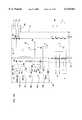
- FIG. 1is an exploded view of a chassis constructed in accordance with the principles of the present invention
- FIG. 2is a front perspective view of a jack in accordance with the principles of the present invention.
- FIG. 3is a rear perspective view of the jack of FIG. 2;
- FIG. 4is a side view of the jack of FIG. 2;
- FIG. 5is a front perspective view of an another jack in accordance with the principles of the present invention.
- FIG. 6is a rear perspective view of the jack of FIG. 5;
- FIG. 7is a side view of the jack of FIG. 5;
- FIG. 8is a front perspective view of jack mount in accordance with the principles of the present invention.
- FIG. 9is a front view of a portion of the jack mount of FIG. 8;
- FIG. 10is a cross-sectional view taken along section line 10--10 of FIG. 9;
- FIG. 11is a cross-sectional view taken along section line 11--11 of FIG. 9;
- FIG. 12is a rear perspective view of the jack mount of FIG. 8;
- FIG. 13is a rear view of the jack mount of FIG. 8;
- FIG. 14is an assembly view of the jack mount of FIG. 8;
- FIG. 15is a front exploded view of a jack mount and twisted pair rear interface assembly in accordance with the principles of the present invention.
- FIG. 16is a rear exploded view of the jack mount and twisted pair rear interface assembly of FIG. 15;
- FIG. 17is a side assembled view of the jack mount and twisted pair rear interface assembly of FIG. 15;
- FIG. 18is a schematic circuit diagram corresponding to the jack mount and twisted pair rear interface assembly of FIG. 15;
- FIG. 19is a front exploded view of a jack mount and coaxial rear interface assembly in accordance with the principles of the present invention.
- FIG. 20is a rear perspective view of the coaxial rear interface assembly of FIG. 19;
- FIG. 21is an exploded view of a connector constructed in accordance with the principles of the present invention.
- FIG. 22is an assembled side view of the connector of FIG. 21;
- FIG. 23is a cross-sectional view taken along section line 23--23 of FIG. 22;
- FIG. 24is an exploded view of another connector constructed in accordance with the principles of the present invention.
- FIG. 25is an assembled side view of the connector of FIG. 24;
- FIG. 26is a cross-sectional view taken along section line 26--26 of FIG. 25;
- FIG. 27is an exploded view of the coaxial rear interface assembly of FIG. 20;
- FIG. 28is a rear view of the coaxial rear interface assembly of FIG. 20;
- FIG. 29is an enlarged view of a portion of FIG. 28.
- FIG. 30is an enlarged view of another portion of FIG. 28.
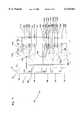
- FIG. 1is an exploded view of an embodiment of a chassis 20 for housing a plurality of jack mounts 22. For clarity, only two jack mounts 22 are shown in FIG. 1. However, it will be appreciated that the chassis 20 is adapted for housing a plurality of jack mounts 22. To conform with conventional international standards, the chassis 20 can house 16 jack mounts 22 and have a length of about 19 inches. Alternatively, in accordance with standard United States specifications, the chassis could be configured to house 21 jacks and have a length of about 23 inches. Of course, other sizes and numbers of jack mounts could also be used.
- the chassis 20includes a top piece 24 positioned opposite from a bottom piece 26.
- the top and bottom pieces 24 and 26are interconnected by left and right side walls 28 and 30.
- the chassis 20also includes a front side 32 positioned opposite from a back side 34.
- the top piece 24includes separate front and back components 23 and 25.
- the front component 23is connected to the chassis 20 by fasteners (e.g., screws) that extend through a front lip 27 of the front component 23 and engage front tabs 29 provided on the side walls 28 and 30.
- the rear component 25is connected to the chassis 20 by fasteners (e.g., screws) that extend downward through top tabs 31 provided on the side walls 28 and 30.
- the rear component 25defines a recessed lip 35 for receiving a rear portion of the front component 23 to form a joint thereinbetween.
- the removable front component 23assists in inserting or removing the jack mounts 22 into or from the chassis 20.
- a wire tray door 36is connected to the bottom piece 26 adjacent the front side 32 of the housing 20.
- a hinge 37allows the door 36 to pivot between horizontal and vertical orientations. Latches 39 hold the door 36 in the vertical orientation.
- a rear flange 38projects upward from the bottom piece 26 adjacent the back side 34 of the chassis 20.
- the rear flange 38defines a plurality of notches or cutaway portions 40.
- a plurality of mounting flanges 42project upward from the bottom piece 26 between the front and back sides 32 and 34 of the chassis 20.
- the mounting flanges 42are adapted for connecting the jack mounts 22 to the chassis 20.
- the mounting flanges 42are shown including holes for allowing the jack mounts 22 to be screwed or bolted to the mounting flanges 42.
- the mounting flanges 42define cutaway portions 44 that correspond to alternating ones of the cutaway portions 40 defined by the rear flange 38.
- Cover members 46are positioned between the mounting flanges 42 and the rear flange 38.
- the cover members 46define recesses 48 that align with the cutaway portions 40 and 44 respectively defined by the rear flange 38 and the mounting flanges 42.
- the cover members 46function to conceal screws or other types of connecting members used to connect the jack mounts 22 to the mounting flanges 42.
- coaxial rear interfacesdescribed later in the specification
- the cutaway portions 40 and 44 and the recesses 48provide clearance for allowing the coaxial connectors to be accessed. In this manner, the height of the chassis 20 can be minimized while still providing access to the lowermost coaxial connectors.
- the chassis 20also includes a cover plate 50 connected below the top piece 24 of the chassis 20.
- a power strip 52is connected to the front cover plate 50.
- the power strip 52includes a plurality of electrical receptacles 54 electrically connected to a main power connector 56.
- the receptacles 54align with and are set behind alignment openings 58 defined by the cover plate 50.
- the jack mount 22is part of a jack assembly including odd jacks 62a, even jacks 62b, and a rear interface assembly 64.
- the rear interface assembly 64includes a dielectric support 66, and a circuit board 68 positioned between the dielectric support 66 and the jack mount 22.
- the odd and even jacks 62a and 62bpreferably have different configurations such that when the jacks 62a and 62b are mounted within the jack mount 22, plug bores defined by the jacks 62a and 62b are vertically staggered relative to one another.
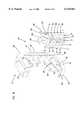
- FIGS. 2-4illustrate one of the odd jacks 62a in isolation from the jack mount 22.
- the jack 62aincludes a dielectric jack body 70a.
- the dielectric jack body 70aincludes a top side 72a and a bottom side 74a arranged and configured to slidingly interface with the jack mount 22.
- the jack body 70aalso includes a front side 76a positioned opposite from a back side 78a.
- the top side 72a of the jack body 70aincludes an elongated guide member 80a that extends between the front and back sides 76a and 78a of the jack body 70a. As best shown in FIG.
- the guide member 80atapers laterally outward as it extends from the back side 78a toward the front side 76a
- Guide surfaces 82aare positioned on opposite sides of the guide member 80a
- the guide surfaces 82ainclude substantially parallel front and rear portions 84a and 86a
- the front and rear portions 84a and 86aare interconnected by ramped portions 88a such that the front portions 84a are elevated relative to the rear portions 86a.
- the bottom side 74a of the jack body 70aincludes a guide member 90a that extends between the back side 78a of the jack body 70a and a transverse wall 92a
- the guide member 90atapers laterally outward as it extends from the back side 78a toward the transverse wall 92a.
- the transverse wall 92aforms a base end of a cantilevered locking member 94a that extends from the transverse wall 92a toward the front side 76a of the jack body 70a.
- a locking tab 96aprojects downward from the locking member 94a.
- a gripping member 98aprojects downward from a free end of the locking member 94a.
- the locking member 94apreferably has a resilient or elastic structure such that the locking member 94a can be flexed upward by pressing upward on the gripping member 98a. By flexing the locking member 94a, the locking member 94a can be moved between a retaining position P a1 (shown in FIG. 4) and a non-retaining position P a2 .
- the bottom side 74aadditionally includes alignment members 100a that project laterally outward from opposite sides of the guide member 90a.
- the alignment members 100aare also connected to the transverse wall 92a and at least partially define alignment notches 102a positioned above the alignment members 100a.
- Guide surfaces 89aare positioned above notches 102a and include front and rear portions 91a and 93a interconnected by a ramped portion 95a.
- the rear portions 93aare elevated relative to the front portions 91a.
- the front side 76a of the jack body 70ais generally planar and defines a light emitting diode (LED) port 104a, a monitor out port 106a, an out port 108a, an in port 110a, and a monitor in port 112a.
- the LED port 104ais sized for receiving an LED 114a.
- Each of the other bores 106a, 108a, 110a and 112ais sized to receive a standard tip-and-ring plug 116a of known dimensions.
- the plug 116aincludes a tip contact 118a, a ring contact 120a and a cylindrical sleeve 122a.
- the back side 78a of the jack body 70ais formed by a generally planar surface 124a that is generally parallel with respect to the front side 76a.
- the planar back surface 124adefines a plurality of back slots 126a each having a generally rectangular shape.
- the jack body 70aalso defines a monitor out chamber 128a, an out chamber 130a positioned below the monitor out chamber 128a, an in chamber 132a positioned below the out chamber 130a, and a monitor in chamber 134a positioned below the in chamber 132a.
- the monitor out chamber 128ais in communication with both the LED port 104a and the monitor out port 106a.
- the LED 114ais mounted within the LED port 104a and includes first and second leads 136a and 138a that project into the monitor out chamber 128a.
- the first lead 136ais contacted by an electrically conductive voltage spring 141a, and the second lead 138a contacts an electrically conductive tracer lamp spring 142a.
- Electrically conductive tip-and-ring springs 145a and 144aare positioned within the monitor out chamber 128a in general alignment with the monitor out port 106a.
- the ring spring 144a and the tip spring 145aare separated by a dielectric spacer 182a that is integrally formed with the jack body 70a.
- a LED return spring 143ais positioned between the ring spring 144a and the tracer lamp spring 142a.
- the ring spring 144aWhen the tip-and-ring plug 116 is inserted within the monitor out port 106a, the ring spring 144a is flexed upwardly while the tip spring 145a is flexed downwardly.
- the ring spring 144acontacts the ring contact 120a, and the tip spring 145a contacts the tip contact 118a of the plug 116a.
- the ring spring 144ais flexed upward, it causes the LED return spring 143a to contact the second lead 138a of the LED 114a thereby illuminating the LED 114a.
- a dielectric pad 184a attached to the ring spring 144aprevents the ring spring 144a from electrically contacting the LED return spring 143a.
- the out chamber 130ais in communication with the out port 108a Electrically conductive tip-and-ring springs 149a and 146a are positioned within the out chamber 130a in general alignment with the out port 108a.
- the tip-and-ring springs 149a and 146aare normally in electrical contact with the respective electrically conductive normal springs 148a and 147a.
- the normal springs 147a and 148aare separated by a dielectric spacer 184a that is integrally formed with the jack body 70a.
- the in chamber 132ais in communication with the in port 110a.
- Electrically conductive tip-and-ring springs 150a and 153aare positioned within the in chamber 132a in general alignment with the in port 110a.
- the tip-and-ring springs 150a and 153aare normally in electrical contact with respective electrically conductive normal springs 151a and 152a.
- Normal springs 151a and 152aare separated by a dielectric spacer 186a that is integrally formed with the jack body 70a.
- the tip-and-ring springs 150a and 153aare respectively disengaged from the normal springs 151a and 152a, and respectively make electrical contact with the tip-and-ring contacts 118a and 120a of the plug 116a.
- An electrically conductive sleeve ground spring 154ais positioned between the in chamber 132a and the monitor in chamber 134a.
- the ground spring 154ais electrically connected to a grounding strip 188a that has electrical contacts corresponding to each of the ports 106a, 108a, 110a and 112a.
- the contactsare configured to engage the sleeve 122a of the plug 116a when the plug is inserted within the ports 106a, 108a, 110a and 112a.
- the monitor in chamber 134a of the jack body 70ais in communication with the monitor in port 112a.
- Electrically conductive tip-and-ring springs 155a and 156aare positioned within the monitor in chamber 134a in general alignment with the monitor in port 112a.
- a dielectric spacer 190ais positioned between the tip-and-ring springs 155a and 156a.
- the springs 141a-156aare preferably held within the jack body 70a by a dielectric strip 191a.
- the dielectric strip 191ais preferably press-fit or snapped within a corresponding slot defined by the jack body 70a.
- electrically conductive springs 141a-156aeach include portions 141a'-156a' that extend through the slots 126a defined by the back side 78a of the jack body 70a.
- the portions 141a'-156a'project outward from the back side 78a and form generally flat contact members adapted for electrically connecting the springs 141a-156a to a desired structure.
- the portions 141a'-156a'have projection lengths that vary such that the tips of the portions 141a'-156a' are staggered. The staggered tips reduce the insertion force required to connect the jack 62a to a desired structure because all of the tips do not engage the desired structure simultaneously upon insertion.
- FIGS. 5-7illustrate one of the even jacks 62b in isolation from the jack mount 22.
- the jack 62bincludes a dielectric jack body 70b having a top side 72b positioned opposite from a bottom side 74b, and a front side 76b positioned opposite from a back side 78b.
- the top side 72bincludes a laterally tapered guide member 90b, and a resilient locking member 94b having an upwardly projecting locking tab 96b.
- the locking member 94bcan be flexed between a retaining position P b1 and a non-retaining position P b2 .
- a transverse wall 92bis positioned generally between the locking member 94b and the guide member 90b.
- Alignment notches 102bare formed generally below the transverse wall 92b on opposite sides of the guide member 90b.
- Guide surfaces 89bare positioned below the notches 102b on opposite sides of the guide member 90b.
- the guide surfaces 89binclude front portions 91b elevated relative to rear portions 93b, and ramped portions 95b positioned between the front and rear portions 91b and 93b.
- the bottom side 74b of the jack body 70bincludes an elongated guide member 80b extending between the front and back sides 76b and 78b.
- the guide member 80btapers laterally outward as it extends from the back side 78b toward the front side 76b.
- the bottom side 74balso includes guide surfaces 82b positioned on opposite sides of the guide member 80b.
- the guide surfaces 82binclude substantially parallel front and back portions 84b and 86b.
- a ramped portion 88binterconnects the front and back portions 84b and 86b such that the back portions 86b are elevated relative to the front portions 84b.
- the top and bottom sides 72b and 74b of the jack body 70bhave different configurations than the top and bottom sides 72a and 74a of the jack body 70a.
- the top and bottom sides of the jack bodies 70a and 70bhave varying configurations in order to provide a keying function. For example, by varying the configurations of the top and bottom sides of the jack bodies 70a and 70b, a user is prevented from placing the jacks 62a and 62b in the wrong positions on the jack mount 22. The user is also inhibited from inserting the jacks 62a and 62b upside-down into the jack mount 22.
- the front side 76b of the jack body 70bdefines an LED port 104b, a monitor out port 106b, an out port 108b, an in port 110b, and a monitor in port 112b.
- the ports 104b, 106b, 108b, 110b and 112bare arranged in a different pattern than the ports 104a, 106a, 108a, 110a and 112a.
- a larger spacingexists between the monitor out port 106b and the out port 108b as compared to the monitor out port 106a and the out port 108a.
- a reduced spacingexists between the in port 110b and the monitor in port 112b as compared to the in port 110a and the monitor in port 112a.
- the terms "port” and "bore"are intended to be used interchangeably.
- the jack 62bhas similar internal components to those previously described with respect to the jack 62a.
- the jack 62bincludes an LED 114b electrically connected to a voltage spring 141b and a tracer lamp spring 142b by leads 136b and 138b.
- An LED ground spring 143bis used to complete the circuit and light the LED 114b.
- the jack 62balso includes tip-and-ring springs 145b and 144b corresponding to the monitor out port 106b, tip-and-ring springs 149b and 146b corresponding to the out port 108b, tip and ring springs 150b and 153b corresponding to the in port 110b and tip-and-ring springs 155b and 156b corresponding to the monitor in port 112b.
- the ring-and-tip springs 146b and 149bnormally contact respective normal springs 147b and 148b
- tip-and-ring springs 150b and 153bnormally contact respective normal springs 151b and 152b.
- the jack 62balso includes a sleeve ground spring 154b interconnected to a grounding strip 188b having sleeve contacts corresponding to each of the ports 106b, 108b, 110b and 112b.
- the conductive springs 141b-156beach include end portions 141b'-156b' (best shown in FIG. 6) that project outward from the back side 78b of the jack body 70b so as to form electrical contact members. As shown in FIG. 7, the tips of the end portions 141a'-156a' are staggered.
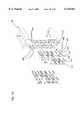
- the jack mount 22is shown in isolation from the chassis 20 with the jacks 62a and 62b removed.
- the jack mount 22includes a mounting body 200 made of a dielectric material.
- the mounting body 200includes a jack receiving piece 202 that can be detachably connected to a cross-connect piece 204.
- the jack receiving piece 202is adapted for housing or holding the jacks 62a and 62b, while the cross-connect piece 204 is adapted for providing cross-connects between jacks.
- the jack receiving piece 202 of the mounting body 200includes a front side 206 positioned opposite from a back side 208.
- the piece 202also includes spaced-apart and substantially parallel top and bottom supports 210 and 212 that extend generally between the front and back sides 206 and 208.
- the top and bottom supports 210 and 212are interconnected by a back wall 214 of the jack receiving piece 202.
- the top support 210, the bottom support 212 and the back wall 214cooperate to define a jack mounting region or recess that opens outward toward the front side 206 of the upper piece 202.
- the jack receiving piece 202 of the mounting body 200defines four separate jack mounting locations ML 1 , ML 2 , ML 3 and ML 4 .
- Jack mounting locations ML 1 and ML 3are adapted to receive the odd jacks 62a, while mounting locations ML 2 and ML 4 are adapted for receiving the even jacks 62b.
- Mounting locations ML 1 and ML 3each include top and bottom channels 224 and 226 respectively formed on the top support 210 and the bottom support 212.
- the top and bottom channels 224 and 226are configured to respectively complement the top and bottom sides 72a and 74a of the jacks 62a.
- the top channels 224are tapered so as to compliment or match the taper of the guide members 80a formed on the top sides 72a of the jack bodies 70a.
- the walls forming the top channels 224have downwardly facing guide surfaces 228 including front portions 230, rear portions 232 and ramped portions 234 that respectively correspond to and complement the front portions 84a, rear portions 86a and ramped portions 88a of the guide surfaces 82a positioned along the top side 72a of the jack body 70a.
- the bottom channels 226are tapered so as to complement or correspond to the taper of the guide member 90a positioned at the bottom side 74a of the jack body 70a.
- the bottom channels 226also include end projections 236 adapted to mate with or fit within the alignment notches 102a formed adjacent the bottom side 74a of the jack body 70a.
- the walls forming the channels 226have upwardly facing guide surfaces 223 including front, rear and ramped portions 225, 227 and 229 that respectively complement the front, rear, and ramped portions 91a, 93a and 95a of the guide surfaces 89a formed on the bottom side of each jack 62a.
- the jack 62ais mounted within one of the mounting locations ML 1 and ML 3 by inserting the rear ends of the guide members 80a and 90a respectively within the top and bottom channels 224 and 226. The jack 62a is then pushed inward toward the back wall 214 of the jack receiving piece 202 causing the guide members 80a and 90a to respectively slide along the top and bottom channels 224 and 226. When the jack 62a has been fully inserted into the jack receiving piece 202, the locking tab 96a of the resilient locking member 94a snaps within a hole 238 (shown in FIG. 11) defined by the bottom support 212.
- the resilient locking member 94ais flexed from the retaining position P a1 to the non-retaining position P a2 such that the locking tab 96a is displaced from the hole 238.
- the jack 62acan then be manually pulled out from the jack receiving piece 202.
- Jack mounting locations ML 2 and ML 4each define top and bottom channels 240 and 242 respectively formed on the top support 210 and the bottom support 212.
- the top channels 240are configured to complement the shape of the top side 72b of the jack 62b.
- the top channels 240are tapered so as to complement the taper of the guide member 90b formed on the top side 72b of the jack 62b.
- the top channels 240also include projections 244 adapted to fit within the alignment notches 102b formed on the jack body 70b adjacent the top side 72b.
- the walls defining the top channel 240include downwardly facing guide surfaces 246 including front portions 248, rear portions 250 and ramped portions 252 that respectively complement the front, rear and ramped portions 91b, 93b and 95b of the guide surfaces 89b formed on the top side 72b of the jack body 70b.
- the top support 210defines openings 254 arranged and configured to receive the locking tab 96b of the jack body 70b when the jack 62b is mounted within the jack mount 22.
- the bottom channels 242are each configured to compliment the bottom side 74b of the jack body 70b.
- the bottom channels 242are tapered to correspond with the taper of the guide member 80b formed on the bottom side 74b of the jack body 70b.
- the walls defining the bottom channels 242include guide surfaces 256 having front, rear and ramped portions 258, 260 and 262 arranged and configured to respectively complement the front, rear and ramped portions 84b, 86b and 88b of the guide surfaces 82b formed on the bottom side 74b of the jack body 70b.
- the top and bottom channels 224, 226 of mounting locations ML 1 and ML 3 , and the top and bottom channels 240, 242 of mounting locations ML 2 and ML 4have been designed in coordination with the top and bottom sides of the jacks 62a and 62b in order to provide a keying function.
- the jack 62acan only be mounted in the jack mount 22 if it is oriented in an upright position and is inserted into either one of the jack mounting locations ML 1 and ML 3 .
- Interference between the top and bottom sides of the jack 62a and the top and bottom channels 240 and 242prevents the jack 62a from being inserted into either one of mounting locations ML 2 and ML 4 .
- the even jack 62bcan only be mounted at mounting locations ML 2 and ML 4 . If the user attempts to insert the jack 62b into either of the jack mounting locations ML 1 and ML 3 , the jack 62b will bind with the top and bottom channels 224 and 226 thereby preventing the jack 62b from being fully inserted into the jack mount 22.
- mounting locations ML 1 and ML 3each include a corresponding pattern or array of openings 264 defined through the back wall 214 of the jack receiving piece 202 of the mounting body 200.
- the openings 264are configured to receive the spring ends 141a'-156a' that project outward from the back side 78a of each jack 62a.
- each of mounting locations ML 2 and ML 4includes a corresponding pattern or array of openings 266 formed through the back wall 214 of the jack receiving piece 202 of the mounting body 200.
- the openings 266are configured to receive the spring ends 141b'-156b' that project outward from the back side 78b of each jack 62b.
- connection pins 268are mounted within each of the openings 264 and 266.
- each of the connection pins 268includes a pin portion 270 that projects outward from the back side 208 of the jack receiving piece 202, and two opposing, cantilevered contact members 272 that are press fit within the openings 264 and 266.
- the connection pins 268are shown connected to elongated installation tools 274 (e.g., the connection pins 268 and the installation tools 274 have been stamped from a common strip of conductive material).
- the installation tools 274maintain a vertical spacing between the connection pins 268 that corresponds to the vertical spacing of the openings 264 and 266.
- the installation tools 274 labeled A and Balign the connection pins 268 in a pattern that corresponds to the pattern defined by the openings 264.
- the installation tools 274 labeled C and Dalign the connection pins 268 in a pattern that corresponds to the pattern defined by the openings 266.
- the installation tools 274are used to press multiple pins 268 in the openings 264 and 266 at once. After the pins have been pressed within the openings 264 and 266, the tools 274 are laterally twisted causing the pins to break-off within the openings 264 and 266.
- the spring extensions 141a'-156a'fit within the openings 264 and are compressed between the opposing contact members 272 of the connection pins 268 such that the spring contacts 141a-156a are electrically connected to the pins 268.
- the spring extensions 141b'-156b'fit within the openings 266 and are compressed between the opposing contact members 272 of the connection pins 268 to provide an electrical interface between the jack springs 141b-156b and the connection pins 268.
- the variable lengths of the spring extensions 141a'-156a' and 141b'-156b'assist in reducing the insertion force required to press the spring extensions between the contact members 272.
- the cross-connect piece 204 of the mounting body 200is adapted for providing cross-connections between jacks.
- wire termination members 276e.g., wire wrap members or posts
- IDCinsulation displacement connectors
- cross-connect pieces 204that are separate from the jack mounting portion 202
- cross-connect pieces having different types of connectorscan be used with the common base to enhance manufacturing efficiency. While wire wrap members and insulation displacement connectors have been specifically described, it will be appreciated that other types of connectors could also be used.
- the cross-connect piece 204includes two spaced-apart tongues 280 (shown in FIG. 8) that are slidingly received within corresponding spaced-apart grooves 282 (shown in FIG. 13) defined by the jack receiving piece 202.
- the tongues 280are aligned with the grooves 282 and the cross-connect piece 204 is slid from the back side 208 of the jack receiving piece 202 toward the front side 206.
- the tongues 280are slid along the grooves 282 until the front face 278 of the cross-connect piece 204 engages a shoulder 284 defined by the piece 202.
- an upwardly projecting tab 286(shown in FIG. 8) formed on the cross-connect piece 204 snaps within a locking opening 288 (shown in FIG. 14) defined by a resilient clip 290 formed at the bottom of the jack receiving piece 202.
- the clip 290is flexed upwardly such that the tab 286 disengages from the opening 288, and the lower piece 204 is pulled in a rearward direction from the upper body 202.
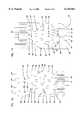
- FIG. 15illustrates the dielectric support 66 of the rear interface assembly 64 removed from the circuit board 68.
- the dielectric support 66includes a front side 300 adapted to face the circuit board 68, and a back side 302 adapted to face away from the circuit board 68.
- the rear interface assembly 64also includes four columns (C a -C d ) and four rows (R a -R d ) of wire termination members 304 press fit within holes defined by the dielectric support 66.
- the wire termination members 304are shown as wire wrap members. However, it will be appreciated that other types of wire termination members such as insulation displacement connectors could also be used.
- the wire termination members 304are adapted to contact plated through-holes 306 in the circuit board 68.
- the wire termination members 276 of the jack mount 22connect with plated through-holes 308 in the circuit board 68.
- the plated through-holes 306are oriented in rows that are positioned between rows R 1 -R 5 .
- the circuit board 68also includes a plurality of additional plated through-holes 310 positioned to make electrical contacts with the connector pins 268 that project outward from the back wall 214 of the jack mount upper piece 202 (shown in FIG. 12).
- the dielectric support 66 of the rear interface assembly 64defines a protective receptacle 318 in which a voltage lead 312, a return lead 314 and a sleeve ground lead 316 are mounted.
- the receptacle 318is adapted to interconnect with the receptacles 54 formed on the power strip 52 of the chassis 20.
- the voltage springs 141a, 141b of the jacksare placed in electrical connection with the voltage leads 312
- the return spring 143a, 143b of the jacks 62a, 62bare placed in electrical connection with the return leads 314
- the ground springs 154a, 154b of the jacks 62a, 62bare placed in electrical connection with the shield ground leads 316.
- the circuit board 68includes a plurality of circuit paths for electrically connecting selected ones of the connection pins 268 to the receptacle leads 312, 314 and 316, to the wire termination members 304 of the rear interface assembly 64, and to the cross-connect wire termination members 276.
- the single circuit board 68is adapted for connecting all four jacks 62a and 62b (shown in FIG. 1) to the leads 312, 314 and 316, and to the their corresponding columns of rear interface wire termination members 304 and cross-connect wire termination members 276.
- the circuit board 68, the jack mount 22 and the dielectric support 66define coaxially aligned openings sized to receive fasteners 69 (e.g., bolts or screws) for connecting the pieces together.
- the fasteners 69extend through captivation washers 71 that are press-fit over the fasteners 69.
- the captivation washers 71 and the fasteners 69hold the jack mount 22, the circuit board 68 and the dielectric support 66 together after assembly and inhibit the pieces from being unintentionally pulled apart prior to connection to the chassis 20.
- the assembly 60is connected to the chassis 20 by threading the fasteners within holes defined by the chassis 20 (e.g., holes defined by the flanges 42 and the coverplate 50 of the chassis 20).
- columns C 1 -C 4 of cross-connect wire termination member 276are respectively connected to jacks positioned in mounting locations ML 1 -ML 4 .
- the wire termination members 276 of row R 1are tracer lamp contacts (TL)
- the wire termination members 276 of row R 2are cross-connect tip-out contacts (XTO)
- the wire termination members 276 of row R 3are cross-connect ring-out contacts (XRO)
- the wire termination members 276 of row R 4are cross-connect tip-in contacts (XTI)
- the wire termination members 276 of row R 5are cross-connect ring-in contacts (XRI).
- Columns C a -C d of the IN/OUT termination members 304are respectively in electrical contact with jacks inserted within jack mounting locations ML 1 -ML 4 .
- the wire termination members 304 of row R aare tip-out contacts (TO)
- the wire termination members 304 forming row R bare ring-out contacts (RO)
- the wire termination members 304 forming row R care tip-in contacts (TI)
- the wire termination members 304 forming row R dare ring-in contacts (RI).
- FIG. 18is a circuit diagram illustrating the electrical connections made when one of the jacks 62b is inserted within jack mounting location ML 4 . It will be appreciated that similar electrical configurations are used to interconnect jacks placed in mounting locations ML 1 -ML 3 with the corresponding columns of contacts C 1 -C 3 and C a -C c .
- the voltage spring 141bis electrically connected to an energized contact point (e.g., the voltage lead 312) for illuminating the LED.
- the tracer lamp spring 142bis connected to the tracer lamp contact TL of column C 4 .
- the return spring 143bis connected to the return lead 314.
- the shield ground spring 154bis connected to the shield ground lead 316.
- the out ring spring 146bis connected to the ring-out contact RO by circuit path 404.
- the ring normal spring 147bis connected to the cross-connect ring-out contact XRO of column C 4 .
- the tip normal spring 148bis connected to the cross-connect tip-out contact XTO of column C 4 .
- Tip spring 149bis connected to the tip-out contact TO of column C d by circuit path 406.
- the monitor out ring spring 144bis connected to circuit path 404
- the monitor out tip spring 145bis connected to circuit path 406.
- Tip spring 150bis connected to the tip-in contact TI of column C d by circuit path 408.
- Tip normal spring 151bis connected to the cross-connect tip-in contact XTI of column C 4
- ring normal spring 152bis electrically connected to the cross-connect ring-in contact XRI of column C 4 .
- Ring spring 153bis connected to the ring-in RI contact of column C d by circuit path 410.
- Tip spring 155bis connected to circuit path 408, while ring spring 156b is connected to circuit path 410.
- Cross-connection of a signal from another jackarrives as an IN signal from cross-connect tip-in and ring-in contacts XTI and XRI of column C 4 .
- the IN signalis output at the tip-in and ring-in contacts TI and RI of column C d .
- the IN signal from a cross-connected jackcan be interrupted and a signal from the inserted plug can be outputted at points TI and RI.
- the OUT signal from contact points TO and ROis interrupted and may be outputted to the tip-and-ring contacts of the plug inserted within the out port 108b.
- a plugis inserted into the monitor port 106b.
- the plugis able to tap into the OUT signals being transmitted through circuit paths 404 and 406.
- the return spring 143bis biased upward into contact with the second lead 138b of the tracer lamp 114b.
- the electrical connection between the second lead 138b and the return spring 143bconnects the LED circuit to the return line 314 thereby illuminating the LED.
- Integrated circuit chip 184bcontrols flashing of the LED 114b as is conventionally known in the art.
- insertion of a plug into the monitor port 106balso grounds the tracer lamp line TL causing illumination of a LED on a jack to which the present jack is cross-connected.
- a plugis inserted into the monitor in port 112b.
- the plugtaps into the in signal being transmitted through circuit path 408 between contacts XTI and TI, and circuit path 410 between contacts XRI and RI.
- FIG. 19illustrates a rear interface assembly 500 adapted to be secured to the jack mount 22.
- the rear interface assembly 500includes eight coaxial connectors 502. Four of the connectors 502 are IN connectors and four are OUT connectors. It will be appreciated that the rear interface assembly 500 and the rear interface assembly 64 are both compatible with or mountable on a common jack. Hence, the same jack can be used to manufacture jack assemblies suited for either twisted pair or coaxial type signals. By using common parts, manufacturing efficiency is enhanced.
- FIGS. 21-23illustrate one of the connectors 502.
- the connector 502is a type 1.6/5.6 connector and includes a grounded main body 512, a center conductor 514, and an insulator 517 mounted between the center conductor 514 and the main body 512.
- the main bodyincludes a nut portion 516 having a generally hexagonal configuration.
- First and second threaded portions 518 and 520are positioned on opposite sides of the nut portion 516.
- the main bodyalso includes a pair of spaced-apart axial projections 522 that project axially from the main body 512.
- the first threaded portion 518is positioned between the projections 522 and the nut portion 516, and the second threaded portion is adapted for connection to a coaxial connector.
- the axial projections 522include notches 524 for facilitating terminating wires.
- the central conductoralso projects outward the main body 512 at a location between the axial projections 522.
- FIGS. 24-26show a BNC style connector 502' suitable for use with the rear interface assembly.
- the connector 502'includes a grounded main body 512', a center conductor 514', and a three-legged insulator 517' mounted between the center conductor 514' and the main body 512'.
- the main bodyincludes a nut portion 516' having a generally hexagonal configuration, and a pair of spaced-apart axial projections 522' that project axially from the main body 512'.
- a threaded portion 518'is positioned axially between the nut portion 516' and the projections 522'.
- the axial projectionsinclude notches 524' for facilitating terminating wires.
- the central conductor 514'projects outward from the main body 512' at a location between the axial projections 522'.
- the rear interface assembly 500includes a dielectric support 506 having a front side 508 that faces the jack mount 22 and a back side 510 that faces away from the jack mount 22.
- a circuit board 507is positioned between the support 506 and the jack mount 22.
- the coaxial connectors 502project outward from the back side 510 to provide access for connections.
- the nut portions 516 of the connectors 502are mounted within hexagon-shaped recesses 509 defined by the support 506. The nut portions 516 seat upon shoulders (not shown) within the recesses 509.
- the circuit board 507, the jack mount 22 and the dielectric support 506define coaxially aligned openings sized to receive fasteners 569 (e.g., bolts or screws) for connecting the pieces together.
- the fasteners 569are preferably press fit through captivation washers (not shown) that hold the pieces 22, 507 and 506 together after assembly.
- the fasteners 569are also used to connect the pieces 22, 507 and 506 to the chassis 20 (shown in FIG. 1).
- a receptacle 513 for connection to one of the receptacles 54 of the power strip 52also projects outward from the back side 510.
- the receptacle 513is arranged to house a voltage lead 562, a return lead 561 and a sleeve ground lead 560.
- the leads 560-562are electrically connected to the circuit board 507.
- the axial projections 522 and center conductors 514extend through the dielectric support 506 and into chambers 546 formed in the front side 508 of the support 506.
- the front side 508 of the support 506also defines a plurality of pockets 525 in which baluns 526 are retained or housed.
- One balun 526corresponds to each connector 502.
- the front side 508further includes a plurality of mounting bosses or pedestals 528 in which a plurality connection pins 530 are press fit or staked.
- the pins 530project outward from the front side 508 and are arranged in a predetermined array that corresponds to an array of contacts (e.g., plated through-holes) of the circuit board 507.
- the circuit board 507typically has a different contact and circuit pathway configuration than the circuit board 68 of the twisted pair rear interface assembly 64.
- the dielectric support 506includes a connector support piece 532 that is detachably connected to a balun housing piece 534.
- the balun housing piece 534includes the generally rectangular pockets 525 for retaining the baluns 526, and the pedestals 528 for mounting the pins 530.
- the connectors 502are secured to the connector support piece 532 by internally threaded lock rings 536 that are threaded on the first threaded portions 518 of the connectors 502.
- the support piece 532includes integrally formed cylindrical sleeves 538 defining through-holes 540 for receiving the connectors 502.
- the cylindrical sleeves 538also include rear seating surfaces 542 against which the lock rings 536 are tightened when the lock rings 536 are threaded on the first threaded portions 518 of the connectors. Interference between the lock rings 536 and the rear seating surfaces 542 prevent the connectors 502 from being pulled from the connector support piece 532. When the pieces 532 and 534 are connected, the rings 536 are concealed or housed within a chamber formed between the pieces 532 and 534.
- the balun housing piece 534defines the chambers 546 into which the extensions 522 and the central conductors 514 of the plugs 502 project when the assembly 500 is assembled.
- the balun housing piece 534defines two curved openings 550 (shown in FIGS. 28-30) for receiving the extensions 522 of the connectors 502, and a circular opening 552 between the curved openings 550 for receiving the central conductors 514 of the plugs 502.
- the housing piece 534also defines a plurality of covers 554 for covering one of each pair of extension members 522.
- the conductive pins 530are divided into eight pairs of tip and ring contacts with each pair of tip and ring contacts corresponding to one of the connectors 502.
- the pairs of pins 530 corresponding to the OUT connectors 502have been labeled TO (tip out) and RO (ring out), while the pairs of pins 530 corresponding to the IN connectors 502 have been labeled TI (tip in) and RI (ring in).
- the balun 526 corresponding to the connectorconverts the unbalanced coaxial signals to balanced twisted pair signals (i.e., tip and ring signals).
- the tip signalis forwarded from the balun 526 to its corresponding TO pin and the ring signal is forwarded to its corresponding RO pin. From the RO and TO pins, the signals are directed to a corresponding jack mounted within the jack mount 22 via circuit pathways on the circuit board 507.
- the baluns 526 corresponding to the IN connectors 502are adapted to convert balanced twisted pair signals into unbalanced coaxial signals. For example, when tip and ring signals from a cross-connected jack arrive at one of the baluns 526, the balun converts the tip and ring signals into a coaxial signal that is outputted through the balun's corresponding IN connector.
- the electrical pathways that connect the TO, RO, TI and RI pins to corresponding jacks mounted within the jack mount 22can be schematically depicted in that same manner as the TO, RO, TI and RI contacts of FIG. 18. It will also be appreciated that the baluns 526 function to match the impedance between the unbalanced coaxial signals and the balanced twisted pair signals.
- the baluns 526preferably comprise torroid magnets each having two wound wires 570 and 572.
- the wires 570, 572respectively terminate at ends 570a, 570b and 572a, 572b.
- the ends 570a, 570bare respectively terminated at the central conductor 514 and one of the extensions 522 of the balun's corresponding connector 502, and the ends 572a, 572b are respectively terminated at the tip pin and the ring pin corresponding to the balun.
Landscapes
- Engineering & Computer Science (AREA)
- Computer Networks & Wireless Communication (AREA)
- Coupling Device And Connection With Printed Circuit (AREA)
- Details Of Connecting Devices For Male And Female Coupling (AREA)
Abstract
Description
Claims (38)
Priority Applications (29)
| Application Number | Priority Date | Filing Date | Title |
|---|---|---|---|
| US09/191,213US6116961A (en) | 1998-11-12 | 1998-11-12 | Jack assembly |
| CA002351228ACA2351228C (en) | 1998-11-12 | 1999-11-05 | Jack assembly |
| MXPA01004740AMXPA01004740A (en) | 1998-11-12 | 1999-11-05 | Jack assembly. |
| HK02102563.1AHK1041370B (en) | 1998-11-12 | 1999-11-05 | Jack assembly |
| AU17145/00AAU765854B2 (en) | 1998-11-12 | 1999-11-05 | Jack assembly |
| AT99960228TATE320091T1 (en) | 1998-11-12 | 1999-11-05 | JACK PLUG DEVICE |
| CNB998155470ACN1292601C (en) | 1998-11-12 | 1999-11-05 | Jack assembly |
| EP07012753AEP1838111A3 (en) | 1998-11-12 | 1999-11-05 | Jack assembly |
| EP05016170.2AEP1608185B1 (en) | 1998-11-12 | 1999-11-05 | Jack assembly |
| DE69930295TDE69930295T2 (en) | 1998-11-12 | 1999-11-05 | JACK PLUG DEVICE |
| BR9915283-5ABR9915283A (en) | 1998-11-12 | 1999-11-05 | Socket assembly |
| PCT/US1999/026271WO2000030219A2 (en) | 1998-11-12 | 1999-11-05 | Jack assembly |
| EP99960228AEP1145385B1 (en) | 1998-11-12 | 1999-11-05 | Jack assembly |
| EP07012754AEP1841241A3 (en) | 1998-11-12 | 1999-11-05 | Jack assembly |
| ARP990105764AAR021257A1 (en) | 1998-11-12 | 1999-11-12 | A FEMALE CONNECTOR PROVISION. |
| US09/470,508US6352451B1 (en) | 1998-11-12 | 1999-12-22 | Jack assembly |
| TW088119759ATW429647B (en) | 1998-11-12 | 2000-01-03 | Jack assembly |
| US10/036,641US6575792B2 (en) | 1998-11-12 | 2001-12-31 | Jack assembly |
| US10/429,179US6799998B2 (en) | 1998-11-12 | 2003-05-02 | Jack assembly |
| AU2003266790AAU2003266790B2 (en) | 1998-11-12 | 2003-12-09 | Jack assembly |
| US10/925,686US6881099B2 (en) | 1998-11-12 | 2004-08-24 | Jack assembly |
| US11/100,263US7083475B2 (en) | 1998-11-12 | 2005-04-05 | Jack insert assembly with cross-connect contacts |
| US11/474,731US7234974B2 (en) | 1998-11-12 | 2006-06-26 | Jack assembly |
| ARP060105808AAR058759A2 (en) | 1998-11-12 | 2006-12-27 | A CROSSED DI GITAL CONNECTION DEVICE (DSX), A TELECOMMUNICATION PROVISION, A FEMALE CONNECTOR STRUCTURE UNDER THIS SUCH TELECOMMUNICATION PROVISION AND A TELECOMMUNICATIONS COMPONENT |
| US11/803,938US7462075B2 (en) | 1998-11-12 | 2007-05-16 | Jack assembly |
| US12/290,910US7658650B2 (en) | 1998-11-12 | 2008-11-05 | Jack assembly arrangement with staggered jack bores |
| US12/655,470US7815472B2 (en) | 1998-11-12 | 2009-12-29 | Jack mount with jacks with normal contacts and vertically staggered jack bores |
| US12/924,901US7901252B2 (en) | 1998-11-12 | 2010-10-06 | Horizontally aligned jack mounts with vertically staggered jack bores |
| US12/931,207US8382528B2 (en) | 1998-11-12 | 2011-01-26 | Jack assembly with vertically staggered jack bores |
Applications Claiming Priority (1)
| Application Number | Priority Date | Filing Date | Title |
|---|---|---|---|
| US09/191,213US6116961A (en) | 1998-11-12 | 1998-11-12 | Jack assembly |
Related Child Applications (1)
| Application Number | Title | Priority Date | Filing Date |
|---|---|---|---|
| US09/470,508ContinuationUS6352451B1 (en) | 1998-11-12 | 1999-12-22 | Jack assembly |
Publications (1)
| Publication Number | Publication Date |
|---|---|
| US6116961Atrue US6116961A (en) | 2000-09-12 |
Family
ID=22704572
Family Applications (12)
| Application Number | Title | Priority Date | Filing Date |
|---|---|---|---|
| US09/191,213Expired - LifetimeUS6116961A (en) | 1998-11-12 | 1998-11-12 | Jack assembly |
| US09/470,508Expired - LifetimeUS6352451B1 (en) | 1998-11-12 | 1999-12-22 | Jack assembly |
| US10/036,641Expired - LifetimeUS6575792B2 (en) | 1998-11-12 | 2001-12-31 | Jack assembly |
| US10/429,179Expired - LifetimeUS6799998B2 (en) | 1998-11-12 | 2003-05-02 | Jack assembly |
| US10/925,686Expired - LifetimeUS6881099B2 (en) | 1998-11-12 | 2004-08-24 | Jack assembly |
| US11/100,263Expired - Fee RelatedUS7083475B2 (en) | 1998-11-12 | 2005-04-05 | Jack insert assembly with cross-connect contacts |
| US11/474,731Expired - Fee RelatedUS7234974B2 (en) | 1998-11-12 | 2006-06-26 | Jack assembly |
| US11/803,938Expired - Fee RelatedUS7462075B2 (en) | 1998-11-12 | 2007-05-16 | Jack assembly |
| US12/290,910Expired - Fee RelatedUS7658650B2 (en) | 1998-11-12 | 2008-11-05 | Jack assembly arrangement with staggered jack bores |
| US12/655,470Expired - Fee RelatedUS7815472B2 (en) | 1998-11-12 | 2009-12-29 | Jack mount with jacks with normal contacts and vertically staggered jack bores |
| US12/924,901Expired - Fee RelatedUS7901252B2 (en) | 1998-11-12 | 2010-10-06 | Horizontally aligned jack mounts with vertically staggered jack bores |
| US12/931,207Expired - Fee RelatedUS8382528B2 (en) | 1998-11-12 | 2011-01-26 | Jack assembly with vertically staggered jack bores |
Family Applications After (11)
| Application Number | Title | Priority Date | Filing Date |
|---|---|---|---|
| US09/470,508Expired - LifetimeUS6352451B1 (en) | 1998-11-12 | 1999-12-22 | Jack assembly |
| US10/036,641Expired - LifetimeUS6575792B2 (en) | 1998-11-12 | 2001-12-31 | Jack assembly |
| US10/429,179Expired - LifetimeUS6799998B2 (en) | 1998-11-12 | 2003-05-02 | Jack assembly |
| US10/925,686Expired - LifetimeUS6881099B2 (en) | 1998-11-12 | 2004-08-24 | Jack assembly |
| US11/100,263Expired - Fee RelatedUS7083475B2 (en) | 1998-11-12 | 2005-04-05 | Jack insert assembly with cross-connect contacts |
| US11/474,731Expired - Fee RelatedUS7234974B2 (en) | 1998-11-12 | 2006-06-26 | Jack assembly |
| US11/803,938Expired - Fee RelatedUS7462075B2 (en) | 1998-11-12 | 2007-05-16 | Jack assembly |
| US12/290,910Expired - Fee RelatedUS7658650B2 (en) | 1998-11-12 | 2008-11-05 | Jack assembly arrangement with staggered jack bores |
| US12/655,470Expired - Fee RelatedUS7815472B2 (en) | 1998-11-12 | 2009-12-29 | Jack mount with jacks with normal contacts and vertically staggered jack bores |
| US12/924,901Expired - Fee RelatedUS7901252B2 (en) | 1998-11-12 | 2010-10-06 | Horizontally aligned jack mounts with vertically staggered jack bores |
| US12/931,207Expired - Fee RelatedUS8382528B2 (en) | 1998-11-12 | 2011-01-26 | Jack assembly with vertically staggered jack bores |
Country Status (13)
| Country | Link |
|---|---|
| US (12) | US6116961A (en) |
| EP (4) | EP1608185B1 (en) |
| CN (1) | CN1292601C (en) |
| AR (2) | AR021257A1 (en) |
| AT (1) | ATE320091T1 (en) |
| AU (1) | AU765854B2 (en) |
| BR (1) | BR9915283A (en) |
| CA (1) | CA2351228C (en) |
| DE (1) | DE69930295T2 (en) |
| HK (1) | HK1041370B (en) |
| MX (1) | MXPA01004740A (en) |
| TW (1) | TW429647B (en) |
| WO (1) | WO2000030219A2 (en) |
Cited By (88)
| Publication number | Priority date | Publication date | Assignee | Title |
|---|---|---|---|---|
| US6238249B1 (en)* | 1999-03-30 | 2001-05-29 | Sharp Kabushiki Kaisha | Opto-electric common jack type connector |
| US6352451B1 (en) | 1998-11-12 | 2002-03-05 | Adc Telecommunications, Inc. | Jack assembly |
| US6422902B1 (en) | 2000-11-10 | 2002-07-23 | Adc Telecommunications, Inc. | Low profile telecommunications jack with lamp switch |
| US6457999B1 (en)* | 2001-04-13 | 2002-10-01 | Adc Telecommunications, Inc. | DSX jack including sliding rear connector |
| US6503105B1 (en) | 2000-11-10 | 2003-01-07 | Adc Telecommunications, Inc. | Telecommunications jack subassembly |
| WO2003030563A2 (en) | 2001-09-28 | 2003-04-10 | Adc Telecommunications, Inc. | Front access dsx assembly |
| US6554652B1 (en)* | 2002-02-15 | 2003-04-29 | Adc Telecommunications, Inc. | Jack assembly including baluns interface; and methods |
| WO2003007624A3 (en)* | 2001-07-13 | 2003-07-17 | Adc Telecommunications Inc | Jack module |
| US6597256B2 (en) | 2001-01-23 | 2003-07-22 | Adc Telecommunications, Inc. | Multi-circuit signal transformer |
| US6619993B2 (en) | 2001-06-01 | 2003-09-16 | Robert Jayne | DSX jack connection system |
| US6632106B2 (en) | 2001-07-24 | 2003-10-14 | Adc Telecommunications, Inc. | Jack; jack assembly; and methods |
| US20030231744A1 (en)* | 2002-06-17 | 2003-12-18 | Hans-Georg Grosse-Boes | Device for providing dual monitoring of digital equipment |
| US20040033716A1 (en)* | 2002-08-14 | 2004-02-19 | Bruce Musolf | Cross-connect jumper assembly having tracer lamp |
| US20040076284A1 (en)* | 2002-10-18 | 2004-04-22 | Baker Scott K. | High density DSX system |
| US20040077318A1 (en)* | 2002-10-18 | 2004-04-22 | Baker Scott K. | Rear access DSX system |
| US6729910B2 (en) | 2001-06-01 | 2004-05-04 | Telect, Inc. | DSX jack LED activation and grounding system |
| US20040097138A1 (en)* | 2002-11-18 | 2004-05-20 | Kha Thong Binh | Modular cross-connect with removable switch assembly |
| US20040110397A1 (en)* | 2002-12-10 | 2004-06-10 | Delta Electronics, Inc. | Assembly structure of adapter |
| WO2004039093A3 (en)* | 2002-10-18 | 2004-08-12 | Adc Telecommunications Inc | Termination panel with fanning strips |
| US20040171286A1 (en)* | 2003-02-28 | 2004-09-02 | Baker Scott K. | Coaxial module with surge protector |
| US20040185710A1 (en)* | 2003-03-19 | 2004-09-23 | Thomas Gregory D | Multi-stack desktop computer/set-top box audio connector |
| US20040194991A1 (en)* | 2003-04-04 | 2004-10-07 | Stockdale Communications, Incorporated | Flush-to-grade vault with wall-mounted cross-connect panels |
| US20040224547A1 (en)* | 2002-10-04 | 2004-11-11 | Eckhart Andrew Karl | Audio jack for patchbays |
| US6830465B2 (en)* | 2001-08-24 | 2004-12-14 | Adc Telecommunications, Inc. | Interconnect chassis and module |
| US20050026506A1 (en)* | 2002-11-18 | 2005-02-03 | Trompeter Electronics, Inc. | Modular cross-connect with hot-swappable modules |
| US6875060B2 (en) | 2002-10-21 | 2005-04-05 | Adc Telecommunications, Inc. | High density patching system |
| US20050122701A1 (en)* | 2003-11-13 | 2005-06-09 | Coffey Joseph C. | Multi-interface patch panel system |
| US20050122676A1 (en)* | 2003-11-13 | 2005-06-09 | Gordon Clark | Patch panel chassis |
| US20050122677A1 (en)* | 2003-11-13 | 2005-06-09 | Gordon Clark | Module with interchangeable card |
| US20050219830A1 (en)* | 2004-03-31 | 2005-10-06 | Coffey Joseph C | Patch panel with modules |
| US20050221660A1 (en)* | 2004-03-31 | 2005-10-06 | Coffey Joseph C | Patch panel with modules |
| US20050281032A1 (en)* | 2004-06-21 | 2005-12-22 | Petersen Cyle D | Press-in place LED for a digital switching cross-connect module |
| US20060012968A1 (en)* | 2004-07-19 | 2006-01-19 | Gonzalez Blazquez Jose L | DSX module with performance monitoring |
| US20060019548A1 (en)* | 2004-07-20 | 2006-01-26 | Baker Scott K | High density patching system with longframe jacks |
| US6992257B2 (en)* | 2001-04-06 | 2006-01-31 | Adc Telecommunications, Inc. | Electronic signal transmission and switching jack |
| US20060067068A1 (en)* | 2004-09-27 | 2006-03-30 | Petersen Cyle D | Digital cross-connect system and rack arrangement |
| DE102005033998A1 (en)* | 2005-07-21 | 2007-02-01 | Adc Gmbh | Insulation displacement connector and device for telecommunications and data technology |
| US20080106881A1 (en)* | 2006-09-01 | 2008-05-08 | Adc Telecommunications, Inc. | Active signal cross-connect system |
| US7393249B2 (en) | 2006-04-21 | 2008-07-01 | Trompeter Electronics, Inc. | Interconnection and monitoring module |
| US20080254647A1 (en)* | 2007-04-12 | 2008-10-16 | Chouanard Harvey J | Flex-x module with board mounted baluns |
| US20100135631A1 (en)* | 2004-11-03 | 2010-06-03 | Adc Telecommunications, Inc. | Fiber optic module and system including rear connectors |
| US20110116748A1 (en)* | 2009-10-16 | 2011-05-19 | Adc Telecommunications, Inc. | Managed connectivity in fiber optic systems and methods thereof |
| US20110228473A1 (en)* | 2010-02-12 | 2011-09-22 | Chad Anderson | Communications bladed panel systems |
| US8346045B2 (en) | 2006-02-13 | 2013-01-01 | Adc Telecommunications, Inc. | Fiber optic splitter module |
| US8565572B2 (en) | 2010-06-23 | 2013-10-22 | Adc Telecommunications, Inc. | Telecommunications assembly |
| US8690593B2 (en) | 2010-02-12 | 2014-04-08 | Adc Telecommunications, Inc. | Managed fiber connectivity systems |
| US8696369B2 (en) | 2010-09-09 | 2014-04-15 | Adc Telecommunications, Inc. | Electrical plug with main contacts and retractable secondary contacts |
| US8715012B2 (en) | 2011-04-15 | 2014-05-06 | Adc Telecommunications, Inc. | Managed electrical connectivity systems |
| US8757895B2 (en) | 2011-04-15 | 2014-06-24 | Adc Telecommunications, Inc. | Managed fiber connectivity systems |
| US8897637B2 (en) | 2009-04-22 | 2014-11-25 | Adc Gmbh | Method and arrangement for identifying at least one object |
| US8992261B2 (en) | 2010-10-22 | 2015-03-31 | Adc Telecommunications, Inc. | Single-piece plug nose with multiple contact sets |
| US8992260B2 (en) | 2009-10-16 | 2015-03-31 | Adc Telecommunications, Inc. | Managed connectivity in electrical systems and methods thereof |
| US9054440B2 (en) | 2009-10-19 | 2015-06-09 | Adc Telecommunications, Inc. | Managed electrical connectivity systems |
| US9064022B2 (en) | 2011-05-17 | 2015-06-23 | Adc Telecommunications, Inc. | Component identification and tracking system for telecommunication networks |
| US9093796B2 (en) | 2012-07-06 | 2015-07-28 | Adc Telecommunications, Inc. | Managed electrical connectivity systems |
| US9182563B2 (en) | 2011-03-31 | 2015-11-10 | Adc Telecommunications, Inc. | Adapter plate for fiber optic module |
| US9203198B2 (en) | 2012-09-28 | 2015-12-01 | Commscope Technologies Llc | Low profile faceplate having managed connectivity |
| US9219543B2 (en) | 2012-07-11 | 2015-12-22 | Commscope Technologies Llc | Monitoring optical decay in fiber connectivity systems |
| US9239442B2 (en) | 2010-04-27 | 2016-01-19 | Adc Communications (Shanghai) Co., Ltd. | Fiber optic module and chassis |
| US9285557B2 (en) | 2012-06-27 | 2016-03-15 | Tyco Electronics Raychem Bvba | High density telecommunications chassis with cable management |
| US9285552B2 (en) | 2013-02-05 | 2016-03-15 | Commscope Technologies Llc | Optical assemblies with managed connectivity |
| US9301030B2 (en) | 2013-11-11 | 2016-03-29 | Commscope Technologies Llc | Telecommunications module |
| US9379501B2 (en) | 2013-02-05 | 2016-06-28 | Commscope Technologies Llc | Optical assemblies with managed connectivity |
| US9395509B2 (en) | 2014-06-23 | 2016-07-19 | Commscope Technologies Llc | Fiber cable fan-out assembly and method |
| US9417401B2 (en) | 2011-09-06 | 2016-08-16 | Commscope Technologies Llc | Adapter for fiber optic module |
| US9423570B2 (en) | 2013-02-05 | 2016-08-23 | Commscope Technologies Llc | Optical assemblies with managed connectivity |
| US9453971B2 (en) | 2012-07-11 | 2016-09-27 | Commscope Technologies Llc | Managed fiber connectivity systems |
| US9470742B2 (en) | 2012-08-03 | 2016-10-18 | Commscope Technologies Llc | Managed fiber connectivity systems |
| US9500814B2 (en) | 2014-03-26 | 2016-11-22 | Commscope Technologies Llc | Optical adapter module with managed connectivity |
| US9521766B2 (en) | 2012-06-27 | 2016-12-13 | CommScope Connectivity Belgium BVBA | High density telecommunications systems with cable management and heat dissipation features |
| US9798096B2 (en) | 2014-02-07 | 2017-10-24 | Commscope Technologies Llc | Managed fiber connectivity systems |
| US10031305B2 (en) | 2012-12-19 | 2018-07-24 | CommScope Connectivity Belgium BVBA | Distribution device with incrementally added splitters |
| US10162131B2 (en) | 2015-08-21 | 2018-12-25 | Commscope Technologies Llc | Telecommunications module |
| US10222571B2 (en) | 2016-04-07 | 2019-03-05 | Commscope Technologies Llc | Telecommunications module and frame |
| US10234648B2 (en) | 2007-08-06 | 2019-03-19 | Commscope Technologies Llc | Fiber optic enclosure with internal cable spool |
| US10371914B2 (en) | 2011-06-24 | 2019-08-06 | Commscope Technologies Llc | Fiber termination enclosure with modular plate assemblies |
| US10514520B2 (en) | 2014-10-27 | 2019-12-24 | Commscope Technologies Llc | Fiber optic cable with flexible conduit |
| US10606009B2 (en) | 2015-12-01 | 2020-03-31 | CommScope Connectivity Belgium BVBA | Cable distribution system with fan out devices |
| US10606019B2 (en) | 2015-07-31 | 2020-03-31 | Commscope Technologies Australia Pty Ltd | Cable breakout assembly |
| US10627592B2 (en) | 2007-05-07 | 2020-04-21 | Commscope Technologies Llc | Fiber optic assembly with cable spool |
| US10637220B2 (en) | 2016-01-28 | 2020-04-28 | CommScope Connectivity Belgium BVBA | Modular hybrid closure |
| US10732370B2 (en) | 2014-06-17 | 2020-08-04 | CommScope Connectivity Belgium BVBA | Cable distribution system |
| US10890730B2 (en) | 2016-08-31 | 2021-01-12 | Commscope Technologies Llc | Fiber optic cable clamp and clamp assembly |
| US10914909B2 (en) | 2016-10-13 | 2021-02-09 | Commscope Technologies Llc | Fiber optic breakout transition assembly incorporating epoxy plug and cable strain relief |
| US11131821B2 (en) | 2016-03-18 | 2021-09-28 | Commscope Technologies Llc | Optic fiber cable fanout conduit arrangements; components, and methods |
| US11131822B2 (en) | 2017-05-08 | 2021-09-28 | Commscope Technologies Llc | Fiber-optic breakout transition assembly |
| US20220416453A1 (en)* | 2021-06-29 | 2022-12-29 | Ford Global Technologies, Llc | Header connector pin arrangement |
| USRE49374E1 (en) | 2003-09-08 | 2023-01-17 | Commscope Technologies Llc | Fiber optic cable and furcation module |
Families Citing this family (29)
| Publication number | Priority date | Publication date | Assignee | Title |
|---|---|---|---|---|
| IT1318039B1 (en)* | 2000-06-21 | 2003-07-21 | Cpe Italia S P A | MODULAR AND EXPANDABLE PANEL OF BIDIRECTIONAL CONNECTION, EQUIPPED WITH A MULTIPLICITY OF DOORS, EACH AVERAGE CONVERTER, ABLE |
| US7070457B2 (en) | 2002-07-19 | 2006-07-04 | Adc Telecommunications, Inc. | Telecommunications connector |
| US6830486B2 (en) | 2002-07-19 | 2004-12-14 | Adc Telecommunications, Inc. | Digital switching cross-connect module |
| US7239699B2 (en) | 2002-07-19 | 2007-07-03 | Adc Telecommunications, Inc. | Monitor network for a digital switching cross-connect module |
| JP4232150B2 (en)* | 2003-06-27 | 2009-03-04 | 三菱電機株式会社 | Terminal box |
| US6848948B1 (en)* | 2003-11-03 | 2005-02-01 | Adc Telecommunications, Inc. | Jack with modular mounting sleeve |
| CA2558996A1 (en)* | 2004-03-08 | 2005-09-22 | Adc Telecommunications, Inc. | Fiber access terminal |
| US6994561B2 (en)* | 2004-05-13 | 2006-02-07 | Tyco Electronics Corporation | Cross connect interface module |
| US7175455B2 (en)* | 2005-04-15 | 2007-02-13 | Adc Telecommunications, Inc. | High density coaxial switching jack |
| US7244131B1 (en) | 2006-04-21 | 2007-07-17 | Adc Telecommunications, Inc. | High density coaxial jack |
| US7591677B2 (en) | 2006-04-21 | 2009-09-22 | Adc Telecommunications, Inc. | High density coaxial jack and panel |
| JP4665933B2 (en)* | 2006-07-04 | 2011-04-06 | セイコーエプソン株式会社 | Document editing support apparatus, program, and storage medium |
| US7912501B2 (en) | 2007-01-05 | 2011-03-22 | Apple Inc. | Audio I/O headset plug and plug detection circuitry |
| CN101689738B (en)* | 2007-05-23 | 2013-02-27 | Fci公司 | Electrical connector with staggered single-ended contacts |
| US7789697B2 (en)* | 2007-06-11 | 2010-09-07 | Apple Inc. | Plug detection mechanisms |
| US7488209B2 (en)* | 2007-06-18 | 2009-02-10 | Commscope Inc. Of North Carolina | Coaxial connector with insulator member including elongate hollow cavities and associated methods |
| EP2198328B1 (en) | 2007-10-09 | 2018-09-26 | ADC Telecommunications, INC. | Mini drop terminal |
| US7903923B2 (en)* | 2007-10-09 | 2011-03-08 | Adc Telecommunications, Inc. | Drop terminal releasable engagement mechanism |
| US20090113648A1 (en)* | 2007-11-07 | 2009-05-07 | Vaynberg Victoria | Brush with an internal compartment |
| AU2008229732B2 (en)* | 2008-04-10 | 2014-08-28 | Tyco Electronics Services Gmbh | Electrical connector |
| KR100963424B1 (en)* | 2008-07-23 | 2010-06-15 | 한국전자통신연구원 | Scalable video decoder and control method thereof |
| JP2011077022A (en)* | 2009-09-03 | 2011-04-14 | Sumitomo Wiring Syst Ltd | Board terminal |
| TWM396512U (en)* | 2010-07-30 | 2011-01-11 | Tyco Electronics Holdings Bermuda No 7 Ltd | Card-edge connector |
| US8535065B2 (en)* | 2012-01-09 | 2013-09-17 | Tyco Electronics Corporation | Connector assembly for interconnecting electrical connectors having different orientations |
| US8771018B2 (en)* | 2012-05-24 | 2014-07-08 | Tyco Electronics Corporation | Card edge connector |
| US10205291B2 (en)* | 2015-02-06 | 2019-02-12 | Masimo Corporation | Pogo pin connector |
| BR112017016302B1 (en) | 2015-02-06 | 2022-12-06 | Masimo Corporation | PHYSIOLOGICAL SENSOR MANUFACTURING METHOD WITH EFFICIENT FLEXIBLE CIRCUIT |
| CN107221820B (en)* | 2017-06-29 | 2024-02-27 | 深圳市深台帏翔电子有限公司 | Terminal equipment and integrated connector thereof |
| CN113571932A (en)* | 2021-07-21 | 2021-10-29 | 中航光电科技股份有限公司 | High-speed connector transmission module and high-speed connector thereof |
Citations (20)
| Publication number | Priority date | Publication date | Assignee | Title |
|---|---|---|---|---|
| US3852703A (en)* | 1973-01-05 | 1974-12-03 | Porta Syst | Modular jack strip assembly |
| US4548453A (en)* | 1983-03-11 | 1985-10-22 | Amp Incorporated | Right angle coaxial plug connector |
| US4749968A (en)* | 1985-12-13 | 1988-06-07 | Adc Telecommunications, Inc. | Jack device |
| US4770639A (en)* | 1987-03-02 | 1988-09-13 | Switchcraft, Inc. | Channelized jackfield |
| US4820200A (en)* | 1987-02-13 | 1989-04-11 | Switchcraft, Inc. | Slab-like jack module |
| US4840568A (en)* | 1987-03-31 | 1989-06-20 | Adc Telecommunications, Inc. | Jack assembly |
| US4861281A (en)* | 1988-09-01 | 1989-08-29 | Telect, Inc. | Electrical jack unit |
| US4975087A (en)* | 1989-12-18 | 1990-12-04 | Telect, Inc. | Telecommunication bantam jack module |
| US5145416A (en)* | 1989-12-19 | 1992-09-08 | Adc Telecommunications, Inc. | Jack assembly |
| US5170327A (en)* | 1990-11-05 | 1992-12-08 | Adc Telecommunications, Inc. | Distal distribution frame module |
| US5199878A (en)* | 1990-11-15 | 1993-04-06 | Adc Telecommunications, Inc. | Plug-in jack card for normally closed contacts |
| US5393249A (en)* | 1993-06-30 | 1995-02-28 | Adc Telecommunications, Inc. | Rear cross connect DSX system |
| US5413494A (en)* | 1992-10-05 | 1995-05-09 | Adc Telecommunications, Inc. | Jack module assembly |
| US5417588A (en)* | 1993-11-15 | 1995-05-23 | Adc Telecommunications, Inc. | Coax connector with center pin locking |
| US5467062A (en)* | 1992-04-02 | 1995-11-14 | Adc Telecommunications, Inc. | Miniature coax jack module |
| WO1996038884A1 (en)* | 1995-05-31 | 1996-12-05 | Telect, Inc. | Telecommunication jack module with interchangeable back plane |
| US5634822A (en)* | 1994-11-14 | 1997-06-03 | Augat Inc. | Miniature telephone jack and rack system |
| US5685741A (en)* | 1996-06-27 | 1997-11-11 | Adc Telecommunications, Inc. | On demand plug-in jack card and monitor frame |
| US5738546A (en)* | 1994-12-01 | 1998-04-14 | Adc Telecommunications, Inc. | Printed circuit board mounted jack |
| US5938478A (en)* | 1998-02-05 | 1999-08-17 | Telect, Inc. | Jack assembly & panel system |
Family Cites Families (30)
| Publication number | Priority date | Publication date | Assignee | Title |
|---|---|---|---|---|
| US13346A (en) | 1855-07-31 | Fan-blower | ||
| US64611A (en) | 1867-05-07 | Improved medical compound | ||
| US22559A (en) | 1859-01-11 | Satjsage-sttjteeb | ||
| DE3200420C2 (en) | 1982-01-09 | 1984-09-06 | Phönix Elektrizitätsgesellschaft H. Knümann GmbH & Co KG, 4933 Blomberg | Terminal block |
| EP0190635B1 (en) | 1985-01-30 | 1989-04-05 | Siemens Aktiengesellschaft | Gas laser with a frequency-selection dielectric layer system |
| US4753609A (en) | 1985-08-12 | 1988-06-28 | Adc Telecommunications, Inc. | Lamp receiving apparatus |
| US4870753A (en) | 1985-08-12 | 1989-10-03 | Adc Telecommunications, Inc | Method of manufacturing a light socket |
| US4826439A (en)* | 1987-03-02 | 1989-05-02 | Switchcraft, Inc. | Self-latching lamp jack |
| US4797114A (en)* | 1987-03-02 | 1989-01-10 | Switchcraft, Inc. | Jack circuit board assembly |
| US4768961A (en) | 1987-10-09 | 1988-09-06 | Switchcraft, Inc. | Jackfield with front removable jack modules having lamp assemblies |
| US4784609A (en) | 1987-10-09 | 1988-11-15 | Switchcraft, Inc. | Jack module with lamp assembly |
| CA1323978C (en)* | 1989-06-28 | 1993-11-09 | James Fisher | Inserting pins into printed circuit boards |
| US4976634A (en)* | 1989-08-31 | 1990-12-11 | Amp Incorporated | Means and method of securing an insert in a shell |
| US5092029A (en)* | 1990-04-27 | 1992-03-03 | Northern Telecom Limited | Apparatus for loading pins for circuit boards |
| US5439395A (en)* | 1993-08-30 | 1995-08-08 | At&T Corp. | DSX jack |
| US5546282A (en)* | 1995-05-02 | 1996-08-13 | Telect, Inc. | Telecommunication network digital cross-connect panels having insertable modules with printed circuit board mounted coaxial jack switches |
| US5658170A (en)* | 1995-09-26 | 1997-08-19 | Hon Hai Precision Ind. Co., Ltd. | Cable connector assembly |
| US5885096A (en) | 1997-04-04 | 1999-03-23 | Adc Telecommunications, Inc. | Switching coaxial jack |
| US5879197A (en) | 1997-11-17 | 1999-03-09 | Adc Telecommunications, Inc. | Jack module |
| US6116961A (en) | 1998-11-12 | 2000-09-12 | Adc Telecommunications, Inc. | Jack assembly |
| US6358093B1 (en)* | 2001-02-07 | 2002-03-19 | Adc Telecommunications, Inc. | Normal through jack and method |
| US6619993B2 (en)* | 2001-06-01 | 2003-09-16 | Robert Jayne | DSX jack connection system |
| US6626705B2 (en)* | 2001-07-13 | 2003-09-30 | Adc Telecommunications, Inc. | Jack module |
| US6632106B2 (en)* | 2001-07-24 | 2003-10-14 | Adc Telecommunications, Inc. | Jack; jack assembly; and methods |
| US6840815B2 (en)* | 2001-09-28 | 2005-01-11 | Adc Telecommunications, Inc. | Front access DSX assembly |
| US6554652B1 (en)* | 2002-02-15 | 2003-04-29 | Adc Telecommunications, Inc. | Jack assembly including baluns interface; and methods |
| US6918793B2 (en)* | 2002-10-18 | 2005-07-19 | Adc Telecommunications, Inc. | Rear access DSX system |
| US6875060B2 (en)* | 2002-10-21 | 2005-04-05 | Adc Telecommunications, Inc. | High density patching system |
| US7044803B2 (en)* | 2004-07-20 | 2006-05-16 | Adc Telecommunications, Inc. | High density patching system with longframe jacks |
| US7540787B2 (en)* | 2007-04-12 | 2009-06-02 | Adc Telecommunications, Inc. | Flex-X module with board mounted baluns |
- 1998
- 1998-11-12USUS09/191,213patent/US6116961A/ennot_activeExpired - Lifetime
- 1999
- 1999-11-05MXMXPA01004740Apatent/MXPA01004740A/enactiveIP Right Grant
- 1999-11-05ATAT99960228Tpatent/ATE320091T1/ennot_activeIP Right Cessation
- 1999-11-05HKHK02102563.1Apatent/HK1041370B/ennot_activeIP Right Cessation
- 1999-11-05AUAU17145/00Apatent/AU765854B2/ennot_activeCeased
- 1999-11-05EPEP05016170.2Apatent/EP1608185B1/ennot_activeExpired - Lifetime
- 1999-11-05CNCNB998155470Apatent/CN1292601C/ennot_activeExpired - Fee Related
- 1999-11-05EPEP99960228Apatent/EP1145385B1/ennot_activeExpired - Lifetime
- 1999-11-05EPEP07012753Apatent/EP1838111A3/ennot_activeWithdrawn
- 1999-11-05EPEP07012754Apatent/EP1841241A3/ennot_activeWithdrawn
- 1999-11-05DEDE69930295Tpatent/DE69930295T2/ennot_activeExpired - Lifetime
- 1999-11-05CACA002351228Apatent/CA2351228C/ennot_activeExpired - Fee Related
- 1999-11-05WOPCT/US1999/026271patent/WO2000030219A2/enactiveIP Right Grant
- 1999-11-05BRBR9915283-5Apatent/BR9915283A/ennot_activeApplication Discontinuation
- 1999-11-12ARARP990105764Apatent/AR021257A1/ennot_activeApplication Discontinuation
- 1999-12-22USUS09/470,508patent/US6352451B1/ennot_activeExpired - Lifetime
- 2000
- 2000-01-03TWTW088119759Apatent/TW429647B/ennot_activeIP Right Cessation
- 2001
- 2001-12-31USUS10/036,641patent/US6575792B2/ennot_activeExpired - Lifetime
- 2003
- 2003-05-02USUS10/429,179patent/US6799998B2/ennot_activeExpired - Lifetime
- 2004
- 2004-08-24USUS10/925,686patent/US6881099B2/ennot_activeExpired - Lifetime
- 2005
- 2005-04-05USUS11/100,263patent/US7083475B2/ennot_activeExpired - Fee Related
- 2006
- 2006-06-26USUS11/474,731patent/US7234974B2/ennot_activeExpired - Fee Related
- 2006-12-27ARARP060105808Apatent/AR058759A2/ennot_activeApplication Discontinuation
- 2007
- 2007-05-16USUS11/803,938patent/US7462075B2/ennot_activeExpired - Fee Related
- 2008
- 2008-11-05USUS12/290,910patent/US7658650B2/ennot_activeExpired - Fee Related
- 2009
- 2009-12-29USUS12/655,470patent/US7815472B2/ennot_activeExpired - Fee Related
- 2010
- 2010-10-06USUS12/924,901patent/US7901252B2/ennot_activeExpired - Fee Related
- 2011
- 2011-01-26USUS12/931,207patent/US8382528B2/ennot_activeExpired - Fee Related
Patent Citations (20)
| Publication number | Priority date | Publication date | Assignee | Title |
|---|---|---|---|---|
| US3852703A (en)* | 1973-01-05 | 1974-12-03 | Porta Syst | Modular jack strip assembly |
| US4548453A (en)* | 1983-03-11 | 1985-10-22 | Amp Incorporated | Right angle coaxial plug connector |
| US4749968A (en)* | 1985-12-13 | 1988-06-07 | Adc Telecommunications, Inc. | Jack device |
| US4820200A (en)* | 1987-02-13 | 1989-04-11 | Switchcraft, Inc. | Slab-like jack module |
| US4770639A (en)* | 1987-03-02 | 1988-09-13 | Switchcraft, Inc. | Channelized jackfield |
| US4840568A (en)* | 1987-03-31 | 1989-06-20 | Adc Telecommunications, Inc. | Jack assembly |
| US4861281A (en)* | 1988-09-01 | 1989-08-29 | Telect, Inc. | Electrical jack unit |
| US4975087A (en)* | 1989-12-18 | 1990-12-04 | Telect, Inc. | Telecommunication bantam jack module |
| US5145416A (en)* | 1989-12-19 | 1992-09-08 | Adc Telecommunications, Inc. | Jack assembly |
| US5170327A (en)* | 1990-11-05 | 1992-12-08 | Adc Telecommunications, Inc. | Distal distribution frame module |
| US5199878A (en)* | 1990-11-15 | 1993-04-06 | Adc Telecommunications, Inc. | Plug-in jack card for normally closed contacts |
| US5467062A (en)* | 1992-04-02 | 1995-11-14 | Adc Telecommunications, Inc. | Miniature coax jack module |
| US5413494A (en)* | 1992-10-05 | 1995-05-09 | Adc Telecommunications, Inc. | Jack module assembly |
| US5393249A (en)* | 1993-06-30 | 1995-02-28 | Adc Telecommunications, Inc. | Rear cross connect DSX system |
| US5417588A (en)* | 1993-11-15 | 1995-05-23 | Adc Telecommunications, Inc. | Coax connector with center pin locking |
| US5634822A (en)* | 1994-11-14 | 1997-06-03 | Augat Inc. | Miniature telephone jack and rack system |
| US5738546A (en)* | 1994-12-01 | 1998-04-14 | Adc Telecommunications, Inc. | Printed circuit board mounted jack |
| WO1996038884A1 (en)* | 1995-05-31 | 1996-12-05 | Telect, Inc. | Telecommunication jack module with interchangeable back plane |
| US5685741A (en)* | 1996-06-27 | 1997-11-11 | Adc Telecommunications, Inc. | On demand plug-in jack card and monitor frame |
| US5938478A (en)* | 1998-02-05 | 1999-08-17 | Telect, Inc. | Jack assembly & panel system |
Non-Patent Citations (2)
| Title |
|---|
| Eighteen color photos of Telect, Inc. co axial and twisted pair jack assemblies. No date.* |
| Eighteen color photos of Telect, Inc. co-axial and twisted pair jack assemblies. No date. |
Cited By (303)
| Publication number | Priority date | Publication date | Assignee | Title |
|---|---|---|---|---|
| US7815472B2 (en) | 1998-11-12 | 2010-10-19 | Adc Telecommunications, Inc. | Jack mount with jacks with normal contacts and vertically staggered jack bores |
| US20050186851A1 (en)* | 1998-11-12 | 2005-08-25 | Henneberger Roy L. | Jack assembly |
| US20040106328A1 (en)* | 1998-11-12 | 2004-06-03 | Adc Telecommunications, Inc. | Jack assembly |
| US7901252B2 (en) | 1998-11-12 | 2011-03-08 | Adc Telecommunications, Inc. | Horizontally aligned jack mounts with vertically staggered jack bores |
| US7234974B2 (en) | 1998-11-12 | 2007-06-26 | Adc Telecommunications, Inc. | Jack assembly |
| US20110034087A1 (en)* | 1998-11-12 | 2011-02-10 | Adc Telecommunications, Inc. | Horizontally aligned jack mounts with vertically staggered jack bores |
| US20070087634A1 (en)* | 1998-11-12 | 2007-04-19 | Adc Telecommunications, Inc. | Jack assembly |
| US20050026508A1 (en)* | 1998-11-12 | 2005-02-03 | Adc Telecommunications, Inc. | Jack assembly |
| US6575792B2 (en) | 1998-11-12 | 2003-06-10 | Adc Telecommunications, Inc. | Jack assembly |
| US6881099B2 (en) | 1998-11-12 | 2005-04-19 | Adc Telecommunications, Inc. | Jack assembly |
| US6352451B1 (en) | 1998-11-12 | 2002-03-05 | Adc Telecommunications, Inc. | Jack assembly |
| US7658650B2 (en) | 1998-11-12 | 2010-02-09 | Adc Telecommunications, Inc. | Jack assembly arrangement with staggered jack bores |
| US20080032563A1 (en)* | 1998-11-12 | 2008-02-07 | Adc Telecommunications, Inc. | Jack assembly |
| US6799998B2 (en) | 1998-11-12 | 2004-10-05 | Adc Telecommunications, Inc. | Jack assembly |
| US8382528B2 (en) | 1998-11-12 | 2013-02-26 | Adc Telecommunications, Inc. | Jack assembly with vertically staggered jack bores |
| US7083475B2 (en) | 1998-11-12 | 2006-08-01 | Adc Telecommunications, Inc. | Jack insert assembly with cross-connect contacts |
| US20090075522A1 (en)* | 1998-11-12 | 2009-03-19 | Adc Telecommunications, Inc. | Jack assembly |
| US7462075B2 (en) | 1998-11-12 | 2008-12-09 | Adc Telecommunications, Inc. | Jack assembly |
| US6238249B1 (en)* | 1999-03-30 | 2001-05-29 | Sharp Kabushiki Kaisha | Opto-electric common jack type connector |
| US6503105B1 (en) | 2000-11-10 | 2003-01-07 | Adc Telecommunications, Inc. | Telecommunications jack subassembly |
| US6422902B1 (en) | 2000-11-10 | 2002-07-23 | Adc Telecommunications, Inc. | Low profile telecommunications jack with lamp switch |
| US6597256B2 (en) | 2001-01-23 | 2003-07-22 | Adc Telecommunications, Inc. | Multi-circuit signal transformer |
| US6717486B2 (en) | 2001-01-23 | 2004-04-06 | Adc Telecommunications, Inc. | Multi-circuit signal transformer |
| US20090223799A1 (en)* | 2001-04-06 | 2009-09-10 | Adc Telecommunications, Inc. | Electronic signal transmission and switching jack |
| US6992257B2 (en)* | 2001-04-06 | 2006-01-31 | Adc Telecommunications, Inc. | Electronic signal transmission and switching jack |
| US20070199809A1 (en)* | 2001-04-06 | 2007-08-30 | Adc Telecommunications, Inc. | Electronic signal transmission and switching jack |
| US7495188B2 (en) | 2001-04-06 | 2009-02-24 | Adc Telecommunications, Inc. | Electronic signal transmission and switching jack |
| US7968810B2 (en) | 2001-04-06 | 2011-06-28 | Adc Telecommunications, Inc. | Electronic signal transmission and switching jack |
| US7092176B2 (en) | 2001-04-06 | 2006-08-15 | Adc Telecommunications, Inc. | Electronic signal transmission and switching jack |
| US20040259425A1 (en)* | 2001-04-13 | 2004-12-23 | Adc Telecommunications, Inc. | Dsx jack including sliding rear connector |
| EP1793454A3 (en)* | 2001-04-13 | 2007-06-13 | ADC Telecommunications, Inc. | Dsx jack including sliding rear connector |
| WO2002084802A3 (en)* | 2001-04-13 | 2003-12-04 | Adc Telecommunications Inc | Dsx jack indluding sliding rear connector |
| US6457999B1 (en)* | 2001-04-13 | 2002-10-01 | Adc Telecommunications, Inc. | DSX jack including sliding rear connector |
| US6761594B2 (en) | 2001-04-13 | 2004-07-13 | Adc Telecommunications, Inc. | DSX jack including sliding rear connector |
| US6533616B2 (en)* | 2001-04-13 | 2003-03-18 | Adc Telecommunications, Inc. | DSX jack including sliding rear connector |
| EP1793454A2 (en) | 2001-04-13 | 2007-06-06 | ADC Telecommunications, Inc. | Dsx jack including sliding rear connector |
| US6872097B2 (en) | 2001-04-13 | 2005-03-29 | Adc Telecommunications, Inc. | Dsx jack including sliding rear connector |
| US6619993B2 (en) | 2001-06-01 | 2003-09-16 | Robert Jayne | DSX jack connection system |
| US6729910B2 (en) | 2001-06-01 | 2004-05-04 | Telect, Inc. | DSX jack LED activation and grounding system |
| WO2003007624A3 (en)* | 2001-07-13 | 2003-07-17 | Adc Telecommunications Inc | Jack module |
| US6626705B2 (en) | 2001-07-13 | 2003-09-30 | Adc Telecommunications, Inc. | Jack module |
| US6632106B2 (en) | 2001-07-24 | 2003-10-14 | Adc Telecommunications, Inc. | Jack; jack assembly; and methods |
| US6830465B2 (en)* | 2001-08-24 | 2004-12-14 | Adc Telecommunications, Inc. | Interconnect chassis and module |
| CN100588272C (en)* | 2001-09-28 | 2010-02-03 | Adc电信股份公司 | Front Access DSX Components |
| WO2003030563A3 (en)* | 2001-09-28 | 2004-04-29 | Adc Telecommunications Inc | Front access dsx assembly |
| US7195521B2 (en) | 2001-09-28 | 2007-03-27 | Adc Telecommunications, Inc. | Front access DSX assembly |
| WO2003030563A2 (en) | 2001-09-28 | 2003-04-10 | Adc Telecommunications, Inc. | Front access dsx assembly |
| US20050227544A1 (en)* | 2001-09-28 | 2005-10-13 | Adc Telecommunications, Inc. | Front access DSX assembly |
| KR100946825B1 (en)* | 2001-09-28 | 2010-03-09 | 에이디씨 텔레커뮤니케이션스 인코포레이티드 | Front Access DSB Assembly |
| US6840815B2 (en) | 2001-09-28 | 2005-01-11 | Adc Telecommunications, Inc. | Front access DSX assembly |
| US6554652B1 (en)* | 2002-02-15 | 2003-04-29 | Adc Telecommunications, Inc. | Jack assembly including baluns interface; and methods |
| US20030231744A1 (en)* | 2002-06-17 | 2003-12-18 | Hans-Georg Grosse-Boes | Device for providing dual monitoring of digital equipment |
| US7127042B2 (en) | 2002-06-17 | 2006-10-24 | Adc Telecommunications, Inc. | Device for providing dual monitoring of digital equipment |
| US6743044B2 (en) | 2002-08-14 | 2004-06-01 | Adc Telecommunications, Inc. | Cross-connect jumper assembly having tracer lamp |
| US20040033716A1 (en)* | 2002-08-14 | 2004-02-19 | Bruce Musolf | Cross-connect jumper assembly having tracer lamp |
| US6905363B2 (en) | 2002-08-14 | 2005-06-14 | Adc Telecommunications, Inc. | Cross-connect jumper assembly having tracer lamp |
| US20040219825A1 (en)* | 2002-08-14 | 2004-11-04 | Adc Telecommunications, Inc. | Cross-connect jumper assembly having tracer lamp |
| US20040224547A1 (en)* | 2002-10-04 | 2004-11-11 | Eckhart Andrew Karl | Audio jack for patchbays |
| US7824201B2 (en) | 2002-10-04 | 2010-11-02 | Switchcraft, Inc. | Switch actuated normalling jack for patchbays |
| US7018245B2 (en) | 2002-10-18 | 2006-03-28 | Adc Telecommunications, Inc. | Termination panel with fanning strips and pivotal cover |
| US6918793B2 (en)* | 2002-10-18 | 2005-07-19 | Adc Telecommunications, Inc. | Rear access DSX system |
| WO2004039095A3 (en)* | 2002-10-18 | 2004-08-12 | Adc Telecommunications Inc | Rear access dsx system |
| US20050202728A1 (en)* | 2002-10-18 | 2005-09-15 | Adc Telecommunications, Inc. | Rear access DSX system |
| US20070081659A1 (en)* | 2002-10-18 | 2007-04-12 | Adc Telecommunications, Inc. | High density DSX system |
| CN1706203B (en)* | 2002-10-18 | 2010-08-25 | Adc电信股份有限公司 | Rear access DSX system |
| US6994593B2 (en) | 2002-10-18 | 2006-02-07 | Adc Telecommunications, Inc. | Rear access DSX system |
| US20050186858A1 (en)* | 2002-10-18 | 2005-08-25 | Adc Telecommunications, Inc. | Termination panel with fanning strips |
| US7095844B2 (en) | 2002-10-18 | 2006-08-22 | Adc Telecommunications, Inc. | High density DSX system |
| WO2004039093A3 (en)* | 2002-10-18 | 2004-08-12 | Adc Telecommunications Inc | Termination panel with fanning strips |
| US20040077318A1 (en)* | 2002-10-18 | 2004-04-22 | Baker Scott K. | Rear access DSX system |
| US20040076284A1 (en)* | 2002-10-18 | 2004-04-22 | Baker Scott K. | High density DSX system |
| US6893299B2 (en) | 2002-10-18 | 2005-05-17 | Adc Telecommunications, Inc. | Termination panel with fanning strips |
| US6875060B2 (en) | 2002-10-21 | 2005-04-05 | Adc Telecommunications, Inc. | High density patching system |
| US20040097138A1 (en)* | 2002-11-18 | 2004-05-20 | Kha Thong Binh | Modular cross-connect with removable switch assembly |
| US6752665B2 (en) | 2002-11-18 | 2004-06-22 | Trompeter Electronics, Inc. | Modular cross-connect with removable switch assembly |
| US20050026506A1 (en)* | 2002-11-18 | 2005-02-03 | Trompeter Electronics, Inc. | Modular cross-connect with hot-swappable modules |
| US20040110397A1 (en)* | 2002-12-10 | 2004-06-10 | Delta Electronics, Inc. | Assembly structure of adapter |
| US6851955B2 (en)* | 2002-12-10 | 2005-02-08 | Delta Electronics, Inc. | Assembly structure of adapter having conductive terminal with metal extending portion for conducting with PCB |
| US7306468B2 (en) | 2003-02-28 | 2007-12-11 | Adc Telecommunications, Inc. | Coaxial module with surge protector |
| US20050146828A1 (en)* | 2003-02-28 | 2005-07-07 | Adc Telecommunications, Inc. | Coaxial module with surge protector |
| US20040171286A1 (en)* | 2003-02-28 | 2004-09-02 | Baker Scott K. | Coaxial module with surge protector |
| US6881076B2 (en)* | 2003-02-28 | 2005-04-19 | Adc Telecommunications, Inc. | Coaxial module with surge protector |
| US20040185710A1 (en)* | 2003-03-19 | 2004-09-23 | Thomas Gregory D | Multi-stack desktop computer/set-top box audio connector |
| US20040194991A1 (en)* | 2003-04-04 | 2004-10-07 | Stockdale Communications, Incorporated | Flush-to-grade vault with wall-mounted cross-connect panels |
| US6861584B2 (en) | 2003-04-04 | 2005-03-01 | Stockdale Communications Incorporated | Flush-to-grade vault with wall-mounted cross-connect panels |
| USRE49374E1 (en) | 2003-09-08 | 2023-01-17 | Commscope Technologies Llc | Fiber optic cable and furcation module |
| US7715210B2 (en) | 2003-11-13 | 2010-05-11 | Adc Telecommunications, Inc. | Patch panel chassis |
| US20050122701A1 (en)* | 2003-11-13 | 2005-06-09 | Coffey Joseph C. | Multi-interface patch panel system |
| US20090154129A1 (en)* | 2003-11-13 | 2009-06-18 | Gordon Clark | Patch panel chassis |
| US7453706B2 (en) | 2003-11-13 | 2008-11-18 | Adc Telecommunications, Inc. | Module with interchangeable card |
| US7054163B2 (en) | 2003-11-13 | 2006-05-30 | Adc Telecommunications, Inc. | Multi-interface patch panel system |
| US20050122677A1 (en)* | 2003-11-13 | 2005-06-09 | Gordon Clark | Module with interchangeable card |
| US7495931B2 (en) | 2003-11-13 | 2009-02-24 | Adc Telecommunications, Inc. | Patch panel chassis |
| US20050122676A1 (en)* | 2003-11-13 | 2005-06-09 | Gordon Clark | Patch panel chassis |
| US20050221660A1 (en)* | 2004-03-31 | 2005-10-06 | Coffey Joseph C | Patch panel with modules |
| US7200929B2 (en) | 2004-03-31 | 2007-04-10 | Adc Telecommunications, Inc. | Patch panel with modules |
| US20070163801A1 (en)* | 2004-03-31 | 2007-07-19 | Adc Telecommunications, Inc. | Patch panel with modules |
| US7978480B2 (en) | 2004-03-31 | 2011-07-12 | Adc Telecommunications, Inc. | Patch panel with modules |
| US20050219830A1 (en)* | 2004-03-31 | 2005-10-06 | Coffey Joseph C | Patch panel with modules |
| US7362590B2 (en) | 2004-03-31 | 2008-04-22 | Adc Telecommunications, Inc. | Patch panel with modules |
| US7553063B2 (en) | 2004-06-21 | 2009-06-30 | Adc Telecommunications, Inc. | Press-in place LED for a digital switching cross-connect module |
| US20050281032A1 (en)* | 2004-06-21 | 2005-12-22 | Petersen Cyle D | Press-in place LED for a digital switching cross-connect module |
| WO2006002110A1 (en)* | 2004-06-21 | 2006-01-05 | Adc Telecommunications, Inc. | Press-in placed led for a digital switching cross-connect module |
| US20070223254A1 (en)* | 2004-06-21 | 2007-09-27 | Adc Telecommunications, Inc. | Press-in place LED for a digital switching cross-connect module |
| US7182502B2 (en) | 2004-06-21 | 2007-02-27 | Adc Telecommunications, Inc. | Press-in place LED for a digital switching cross-connect module |
| CN100591146C (en)* | 2004-07-19 | 2010-02-17 | Adc电信公司 | DSX Module with Performance Monitoring |
| US20060012968A1 (en)* | 2004-07-19 | 2006-01-19 | Gonzalez Blazquez Jose L | DSX module with performance monitoring |
| US7764781B2 (en)* | 2004-07-19 | 2010-07-27 | Adc Telecommunications, Inc. | DSX module with performance monitoring |
| US20060019548A1 (en)* | 2004-07-20 | 2006-01-26 | Baker Scott K | High density patching system with longframe jacks |
| US7044803B2 (en) | 2004-07-20 | 2006-05-16 | Adc Telecommunications, Inc. | High density patching system with longframe jacks |
| WO2006083321A1 (en)* | 2004-07-20 | 2006-08-10 | Adc Telecommunications, Inc. | Long frame high density patching system |
| US20060067068A1 (en)* | 2004-09-27 | 2006-03-30 | Petersen Cyle D | Digital cross-connect system and rack arrangement |
| US8331753B2 (en) | 2004-11-03 | 2012-12-11 | Adc Telecommunications, Inc. | Fiber optic module and system including rear connectors |
| US20100135631A1 (en)* | 2004-11-03 | 2010-06-03 | Adc Telecommunications, Inc. | Fiber optic module and system including rear connectors |
| US9964726B2 (en) | 2004-11-03 | 2018-05-08 | Commscope Technologies Llc | Fiber optic module and system including rear connectors |
| US9213159B2 (en) | 2004-11-03 | 2015-12-15 | Commscope Technologies Llc | Fiber optic module and system including rear connectors |
| US8023791B2 (en) | 2004-11-03 | 2011-09-20 | Adc Telecommunications, Inc. | Fiber optic module and system including rear connectors |
| US10359591B2 (en) | 2004-11-03 | 2019-07-23 | Commscope Technologies Llc | Fiber optic module and system including rear connectors |
| US11280974B2 (en) | 2004-11-03 | 2022-03-22 | Comm Scope Technologies LLC | Fiber optic module and system including rear connectors |
| US8705928B2 (en) | 2004-11-03 | 2014-04-22 | Adc Telecommunications, Inc. | Fiber optic module and system including rear connectors |
| US7815439B2 (en) | 2005-07-21 | 2010-10-19 | Adc Gmbh | Insulation displacement plug-in connector and device for telecommunications and data technology |
| DE102005033998A1 (en)* | 2005-07-21 | 2007-02-01 | Adc Gmbh | Insulation displacement connector and device for telecommunications and data technology |
| US20080227329A1 (en)* | 2005-07-21 | 2008-09-18 | Adc Gmbh | Insulation Displacement Plug-In Connector And Device For Telecommunications And Data Technology |
| US10473876B2 (en) | 2006-02-13 | 2019-11-12 | Commscope Technologies Llc | Fiber optic splitter module |
| US9563017B2 (en) | 2006-02-13 | 2017-02-07 | Commscope Technologies Llc | Fiber optic splitter module |
| US11105994B2 (en) | 2006-02-13 | 2021-08-31 | Commscope Technologies Llc | Fiber optic splitter module |
| US11579391B2 (en) | 2006-02-13 | 2023-02-14 | Commscope Technologies Llc | Fiber optic splitter module |
| US12222572B2 (en) | 2006-02-13 | 2025-02-11 | Commscope Technologies Llc | Fiber optic splitter module |
| US8346045B2 (en) | 2006-02-13 | 2013-01-01 | Adc Telecommunications, Inc. | Fiber optic splitter module |
| US8798428B2 (en) | 2006-02-13 | 2014-08-05 | Adc Telecommunications, Inc. | Fiber optic splitter module |
| US7393249B2 (en) | 2006-04-21 | 2008-07-01 | Trompeter Electronics, Inc. | Interconnection and monitoring module |
| US20080106881A1 (en)* | 2006-09-01 | 2008-05-08 | Adc Telecommunications, Inc. | Active signal cross-connect system |
| US20080254647A1 (en)* | 2007-04-12 | 2008-10-16 | Chouanard Harvey J | Flex-x module with board mounted baluns |
| US7540787B2 (en)* | 2007-04-12 | 2009-06-02 | Adc Telecommunications, Inc. | Flex-X module with board mounted baluns |
| US10788642B2 (en) | 2007-05-07 | 2020-09-29 | Commscope Technologies Llc | Fiber optic assembly with cable storage arrangement |
| US12235506B2 (en) | 2007-05-07 | 2025-02-25 | Commscope Technologies Llc | Fiber optic enclosure with external cable spool |
| US10627592B2 (en) | 2007-05-07 | 2020-04-21 | Commscope Technologies Llc | Fiber optic assembly with cable spool |
| US11009671B2 (en) | 2007-05-07 | 2021-05-18 | Commscope Technologies Llc | Fiber optic assembly with cable storage arrangement |
| US10895705B2 (en) | 2007-08-06 | 2021-01-19 | Commscope Technologies Llc | Fiber optic enclosure with internal cable spool |
| US12019301B2 (en) | 2007-08-06 | 2024-06-25 | Commscope Technologies Llc | Fiber optic enclosure with internal cable spool |
| US10234648B2 (en) | 2007-08-06 | 2019-03-19 | Commscope Technologies Llc | Fiber optic enclosure with internal cable spool |
| US10247897B2 (en) | 2007-08-06 | 2019-04-02 | Commscope Technologies Llc | Fiber optic enclosure with internal cable spool |
| US12253734B2 (en) | 2007-08-06 | 2025-03-18 | Commscope Technologies Llc | Fiber optic enclosure with internal cable spool |
| US10495836B2 (en) | 2007-08-06 | 2019-12-03 | Commscope Technologies Llc | Fiber optic payout assembly including cable spool |
| US11573390B2 (en) | 2007-08-06 | 2023-02-07 | Commscope Technologies Llc | Fiber optic enclosure with internal cable spool |
| US10996417B2 (en) | 2007-08-06 | 2021-05-04 | Commscope Technologies Llc | Fiber optic enclosure with internal cable spool and movable cover |
| US10606017B2 (en) | 2007-08-06 | 2020-03-31 | Commscope Technologies Llc | Fiber optic payout assembly including cable spool |
| US10996418B2 (en) | 2007-08-06 | 2021-05-04 | Commscope Technologies Llc | Connecting subscribers to a fiber optic network using a cable spool |
| US10606015B2 (en) | 2007-08-06 | 2020-03-31 | Commscope Technologies Llc | Fiber optic payout assembly including cable spool |
| US10712518B2 (en) | 2007-08-06 | 2020-07-14 | Commscope Technologies Llc | Fiber optic enclosure with lockable internal cable spool |
| US8897637B2 (en) | 2009-04-22 | 2014-11-25 | Adc Gmbh | Method and arrangement for identifying at least one object |
| US12235494B2 (en) | 2009-10-16 | 2025-02-25 | Commscope Technologies Llc | Managed connectivity in fiber optic systems and methods thereof |
| US11191173B2 (en) | 2009-10-16 | 2021-11-30 | Commscope Technologies Llc | Managed connectivity in electrical systems and methods thereof |
| US11630269B2 (en) | 2009-10-16 | 2023-04-18 | Commscope Technologies Llc | Managed connectivity in fiber optic systems and methods thereof |
| US10678001B2 (en) | 2009-10-16 | 2020-06-09 | Commscope Technologies Llc | Managed connectivity in fiber optic systems and methods thereof |
| US8992260B2 (en) | 2009-10-16 | 2015-03-31 | Adc Telecommunications, Inc. | Managed connectivity in electrical systems and methods thereof |
| US9769939B2 (en) | 2009-10-16 | 2017-09-19 | Commscope Technologies Llc | Managed connectivity in electrical systems and methods thereof |
| US9176294B2 (en) | 2009-10-16 | 2015-11-03 | Tyco Electronics Services Gmbh | Managed connectivity in fiber optic systems and methods thereof |
| US9810860B2 (en) | 2009-10-16 | 2017-11-07 | Commscope Technologies Llc | Managed connectivity in fiber optic systems and methods thereof |
| US20110116748A1 (en)* | 2009-10-16 | 2011-05-19 | Adc Telecommunications, Inc. | Managed connectivity in fiber optic systems and methods thereof |
| US8596882B2 (en) | 2009-10-16 | 2013-12-03 | Adc Telecommunications, Inc. | Managed connectivity in fiber optic systems and methods thereof |
| US10470320B2 (en) | 2009-10-16 | 2019-11-05 | Commscope Technologies Llc | Managed connectivity in electrical systems and methods thereof |
| US9967983B2 (en) | 2009-10-16 | 2018-05-08 | Commscope Technologies Llc | Managed connectivity in electrical systems and methods thereof |
| US9401552B2 (en) | 2009-10-16 | 2016-07-26 | Commscope Technologies Llc | Managed connectivity in electrical systems and methods thereof |
| US11231555B2 (en) | 2009-10-16 | 2022-01-25 | Commscope Technologies Llc | Managed connectivity in fiber optic systems and methods thereof |
| US9054440B2 (en) | 2009-10-19 | 2015-06-09 | Adc Telecommunications, Inc. | Managed electrical connectivity systems |
| US10177514B2 (en) | 2009-10-19 | 2019-01-08 | Commscope Technologies Llc | Managed electrical connectivity systems |
| US11862912B2 (en) | 2009-10-19 | 2024-01-02 | Commscope Technologies Llc | Managed electrical connectivity systems |
| US11469560B2 (en) | 2009-10-19 | 2022-10-11 | Commscope Technologies Llc | Managed electrical connectivity systems |
| US10574008B2 (en) | 2009-10-19 | 2020-02-25 | Commscope Technologies Llc | Managed electrical connectivity systems |
| US10958024B2 (en) | 2009-10-19 | 2021-03-23 | Commscope Technologies Llc | Managed electrical connectivity systems |
| US9595797B2 (en) | 2009-10-19 | 2017-03-14 | Commscope Technologies Llc | Managed electrical connectivity systems |
| US9213363B2 (en) | 2010-02-12 | 2015-12-15 | Tyco Electronics Services Gmbh | Communications bladed panel systems |
| US8923013B2 (en) | 2010-02-12 | 2014-12-30 | Adc Telecommunications, Inc. | Communications bladed panel systems |
| US9532481B2 (en) | 2010-02-12 | 2016-12-27 | Commscope Technologies Llc | Communications bladed panel systems |
| US9532482B2 (en) | 2010-02-12 | 2016-12-27 | Commscope Technologies Llc | Communications bladed panel systems |
| US9549484B2 (en) | 2010-02-12 | 2017-01-17 | Commscope Technologies Llc | Communications bladed panel systems |
| US12306444B2 (en) | 2010-02-12 | 2025-05-20 | Commscope Technologies Llc | Managed fiber connectivity systems |
| US20110228473A1 (en)* | 2010-02-12 | 2011-09-22 | Chad Anderson | Communications bladed panel systems |
| US8690593B2 (en) | 2010-02-12 | 2014-04-08 | Adc Telecommunications, Inc. | Managed fiber connectivity systems |
| US10123444B2 (en) | 2010-02-12 | 2018-11-06 | Commscope Technologies Llc | Communications bladed panel systems |
| US10088636B2 (en) | 2010-02-12 | 2018-10-02 | Commscope Technologies Llc | Managed fiber connectivity systems |
| US9632255B2 (en) | 2010-02-12 | 2017-04-25 | Commscope Technologies Llc | Managed fiber connectivity systems |
| US11899246B2 (en) | 2010-02-12 | 2024-02-13 | Commscope Technologies Llc | Managed fiber connectivity systems |
| US9684134B2 (en) | 2010-02-12 | 2017-06-20 | Commscope Technologies Llc | Managed fiber connectivity systems |
| US9265172B2 (en) | 2010-02-12 | 2016-02-16 | Commscope Technologies Llc | Communications bladed panel systems |
| US9417399B2 (en) | 2010-02-12 | 2016-08-16 | Commscope Technologies Llc | Managed fiber connectivity systems |
| US8934253B2 (en) | 2010-02-12 | 2015-01-13 | Adc Telecommunications, Inc. | Communications bladed panel systems |
| US8934252B2 (en) | 2010-02-12 | 2015-01-13 | Adc Telecommunications, Inc. | Communications bladed panel systems |
| US11378755B2 (en) | 2010-02-12 | 2022-07-05 | Commscope Technologies Llc | Managed fiber connectivity systems |
| US9020319B2 (en) | 2010-02-12 | 2015-04-28 | Adc Telecommunications, Inc. | Communications bladed panel systems |
| US9804337B2 (en) | 2010-02-12 | 2017-10-31 | Commscope Technologies Llc | Managed fiber connectivity systems |
| US9140859B2 (en) | 2010-02-12 | 2015-09-22 | Tyco Electronics Services Gmbh | Managed fiber connectivity systems |
| US10983285B2 (en) | 2010-02-12 | 2021-04-20 | Commscope Technologies Llc | Managed fiber connectivity systems |
| US10473864B2 (en) | 2010-02-12 | 2019-11-12 | Commscope Technologies Llc | Managed fiber connectivity systems |
| US9198320B2 (en) | 2010-02-12 | 2015-11-24 | Tyco Electronics Services Gmbh | Communications bladed panel systems |
| US9223105B2 (en) | 2010-02-12 | 2015-12-29 | Commscope Technologies Llc | Communications bladed panel systems |
| US9618719B2 (en) | 2010-04-27 | 2017-04-11 | Adc Telecommunications (Shanghai) Distribution Co., Ltd. | Fiber optic module and chassis |
| US9239442B2 (en) | 2010-04-27 | 2016-01-19 | Adc Communications (Shanghai) Co., Ltd. | Fiber optic module and chassis |
| US10969555B2 (en) | 2010-04-27 | 2021-04-06 | Commscope Telecommunications (Shanghai) Co. Ltd. | Fiber optic module and chassis |
| US10473877B2 (en) | 2010-04-27 | 2019-11-12 | Commscope Telecommunications (Shanghai) Co., Ltd. | Fiber optic module and chassis |
| US11619792B2 (en) | 2010-04-27 | 2023-04-04 | Commscope Telecommunications (Shanghai) Co. Ltd. | Fiber optic module and chassis |
| US10073233B2 (en) | 2010-04-27 | 2018-09-11 | ADC Telecommunications (Shanghai) Distribution Co. Ltd. | Fiber optic module and chassis |
| US12099247B2 (en) | 2010-04-27 | 2024-09-24 | Commscope Telecommunications (Shanghai) Co. Ltd. | Fiber optic module and chassis |
| US10126516B1 (en) | 2010-06-23 | 2018-11-13 | Commscope Technologies Llc | Telecommunications assembly |
| US10884211B2 (en) | 2010-06-23 | 2021-01-05 | Commscope Technologies Llc | Telecommunications assembly |
| US12235504B2 (en) | 2010-06-23 | 2025-02-25 | Commscope Technologies Llc | Telecommunications assembly |
| US8565572B2 (en) | 2010-06-23 | 2013-10-22 | Adc Telecommunications, Inc. | Telecommunications assembly |
| US9995898B2 (en) | 2010-06-23 | 2018-06-12 | Commscope Technologies Llc | Telecommunications assembly |
| US9678296B2 (en) | 2010-06-23 | 2017-06-13 | Commscope Technologies Llc | Telecommunications assembly |
| US11789226B2 (en) | 2010-06-23 | 2023-10-17 | Commscope Technologies Llc | Telecommunications assembly |
| US9341802B2 (en) | 2010-06-23 | 2016-05-17 | Commscope Technologies Llc | Telecommunications assembly |
| US10627593B2 (en) | 2010-06-23 | 2020-04-21 | Commscope Technologies Llc | Telecommunications assembly |
| US10268014B2 (en) | 2010-06-23 | 2019-04-23 | Commscope Technologies Llc | Telecommunications assembly |
| US11402595B2 (en) | 2010-06-23 | 2022-08-02 | Commscope Technologies Llc | Telecommunications assembly |
| US9170392B2 (en) | 2010-06-23 | 2015-10-27 | Tyco Electronics Services Gmbh | Telecommunications assembly |
| US8696369B2 (en) | 2010-09-09 | 2014-04-15 | Adc Telecommunications, Inc. | Electrical plug with main contacts and retractable secondary contacts |
| US8992261B2 (en) | 2010-10-22 | 2015-03-31 | Adc Telecommunications, Inc. | Single-piece plug nose with multiple contact sets |
| US9182563B2 (en) | 2011-03-31 | 2015-11-10 | Adc Telecommunications, Inc. | Adapter plate for fiber optic module |
| US9753238B2 (en) | 2011-03-31 | 2017-09-05 | Commscope Technologies Llc | Adapter plate for fiber optic module |
| US10175442B2 (en) | 2011-03-31 | 2019-01-08 | Commscope Technologies Llc | Adapter plate for fiber optic module |
| US9759874B2 (en) | 2011-04-15 | 2017-09-12 | CommScope Technologies, LLC | Managed fiber connectivity systems |
| US8757895B2 (en) | 2011-04-15 | 2014-06-24 | Adc Telecommunications, Inc. | Managed fiber connectivity systems |
| US9502843B2 (en) | 2011-04-15 | 2016-11-22 | Commscope Technologies Llc | Managed electrical connectivity systems |
| US9147983B2 (en) | 2011-04-15 | 2015-09-29 | Adc Telecommunications, Inc. | Managed electrical connectivity systems |
| US9244229B2 (en) | 2011-04-15 | 2016-01-26 | Commscope Technologies Llc | Managed fiber connectivity systems |
| US8715012B2 (en) | 2011-04-15 | 2014-05-06 | Adc Telecommunications, Inc. | Managed electrical connectivity systems |
| US8944856B2 (en) | 2011-04-15 | 2015-02-03 | Adc Telecommunications, Inc. | Managed electrical connectivity systems |
| US9064022B2 (en) | 2011-05-17 | 2015-06-23 | Adc Telecommunications, Inc. | Component identification and tracking system for telecommunication networks |
| US11988883B2 (en) | 2011-06-24 | 2024-05-21 | Commscope Technologies Llc | Fiber termination enclosure with modular plate assemblies |
| US10371914B2 (en) | 2011-06-24 | 2019-08-06 | Commscope Technologies Llc | Fiber termination enclosure with modular plate assemblies |
| US11327262B2 (en) | 2011-06-24 | 2022-05-10 | Commscope Technologies Llc | Fiber termination enclosure with modular plate assemblies |
| US11624884B2 (en) | 2011-06-24 | 2023-04-11 | Commscope Technologies Llc | Fiber termination enclosure with modular plate assemblies |
| US10935744B2 (en) | 2011-06-24 | 2021-03-02 | Commscope Technologies Llc | Fiber termination enclosure with modular plate assemblies |
| US10502916B2 (en) | 2011-06-24 | 2019-12-10 | Commscope Technologies Llc | Fiber termination enclosure with modular plate assemblies |
| US10139570B2 (en) | 2011-09-06 | 2018-11-27 | Commscope Technologies Llc | Adapter for fiber optic module |
| US10649151B2 (en) | 2011-09-06 | 2020-05-12 | Commscope Technologies Llc | Adapter for fiber optic module |
| US9417401B2 (en) | 2011-09-06 | 2016-08-16 | Commscope Technologies Llc | Adapter for fiber optic module |
| US10182512B2 (en) | 2012-06-27 | 2019-01-15 | CommScope Connectivity Belgium BVBA | High density telecommunications system with cable management and heat dissipation features |
| US9285557B2 (en) | 2012-06-27 | 2016-03-15 | Tyco Electronics Raychem Bvba | High density telecommunications chassis with cable management |
| US9986654B2 (en) | 2012-06-27 | 2018-05-29 | CommScope Connectivity Belgium BVBA | High density telecommunications chassis with cable management |
| US9521766B2 (en) | 2012-06-27 | 2016-12-13 | CommScope Connectivity Belgium BVBA | High density telecommunications systems with cable management and heat dissipation features |
| US9093796B2 (en) | 2012-07-06 | 2015-07-28 | Adc Telecommunications, Inc. | Managed electrical connectivity systems |
| US9437990B2 (en) | 2012-07-06 | 2016-09-06 | Commscope Technologies Llc | Managed electrical connectivity systems |
| US9453971B2 (en) | 2012-07-11 | 2016-09-27 | Commscope Technologies Llc | Managed fiber connectivity systems |
| US20170108653A1 (en)* | 2012-07-11 | 2017-04-20 | Commscope Technologies Llc | Managed fiber connectivity systems |
| US9219543B2 (en) | 2012-07-11 | 2015-12-22 | Commscope Technologies Llc | Monitoring optical decay in fiber connectivity systems |
| US10050703B2 (en) | 2012-07-11 | 2018-08-14 | Commscope Technologies Llc | Monitoring optical decay in fiber connectivity systems |
| US9470742B2 (en) | 2012-08-03 | 2016-10-18 | Commscope Technologies Llc | Managed fiber connectivity systems |
| US9525255B2 (en) | 2012-09-28 | 2016-12-20 | Commscope Technologies Llc | Low profile faceplate having managed connectivity |
| US9203198B2 (en) | 2012-09-28 | 2015-12-01 | Commscope Technologies Llc | Low profile faceplate having managed connectivity |
| US10031305B2 (en) | 2012-12-19 | 2018-07-24 | CommScope Connectivity Belgium BVBA | Distribution device with incrementally added splitters |
| US10545305B2 (en) | 2012-12-19 | 2020-01-28 | CommScope Connectivity Belgium BVBA | Distribution device with incrementally added splitters |
| US9735523B2 (en) | 2013-02-05 | 2017-08-15 | Commscope Connectivity Uk Limited | Optical assemblies with managed connectivity |
| US9285552B2 (en) | 2013-02-05 | 2016-03-15 | Commscope Technologies Llc | Optical assemblies with managed connectivity |
| US10746943B2 (en) | 2013-02-05 | 2020-08-18 | Commscope Technologies Llc | Optical assemblies with managed connectivity |
| US11867952B2 (en) | 2013-02-05 | 2024-01-09 | Commscope Technologies Llc | Optical assemblies with managed connectivity |
| US9423570B2 (en) | 2013-02-05 | 2016-08-23 | Commscope Technologies Llc | Optical assemblies with managed connectivity |
| US11143833B2 (en) | 2013-02-05 | 2021-10-12 | Commscope Technologies Llc | Optical assemblies with managed connectivity |
| US9379501B2 (en) | 2013-02-05 | 2016-06-28 | Commscope Technologies Llc | Optical assemblies with managed connectivity |
| US12235505B2 (en) | 2013-02-05 | 2025-02-25 | Commscope Technologies Llc | Fiber optic cassette arrangement |
| US10012813B2 (en) | 2013-02-05 | 2018-07-03 | Commscope Technologies Llc | Optical assemblies with managed connectivity |
| US11714246B2 (en) | 2013-02-05 | 2023-08-01 | Commscope Technologies Llc | Optical assemblies with contoured base |
| US10268000B2 (en) | 2013-02-05 | 2019-04-23 | Commscope Technologies Llc | Optical assemblies with managed connectivity |
| US11327248B2 (en) | 2013-02-05 | 2022-05-10 | Commscope Technologies Llc | Optical assemblies with managed connectivity |
| US10571641B2 (en) | 2013-02-05 | 2020-02-25 | Commscope Technologies Llc | Optical assemblies with managed connectivity |
| US9778424B2 (en) | 2013-02-05 | 2017-10-03 | Commscope Technologies Llc | Optical assemblies with managed connectivity |
| US9609404B2 (en) | 2013-11-11 | 2017-03-28 | Commscope Technologies Llc | Telecommunications module |
| US10063947B2 (en) | 2013-11-11 | 2018-08-28 | Commscope Technologies Llc | Telecommunications module |
| US9301030B2 (en) | 2013-11-11 | 2016-03-29 | Commscope Technologies Llc | Telecommunications module |
| US9798096B2 (en) | 2014-02-07 | 2017-10-24 | Commscope Technologies Llc | Managed fiber connectivity systems |
| US9995883B2 (en) | 2014-03-26 | 2018-06-12 | Commscope Technologies Llc | Optical adapter module with managed connectivity |
| US9500814B2 (en) | 2014-03-26 | 2016-11-22 | Commscope Technologies Llc | Optical adapter module with managed connectivity |
| US10509177B2 (en) | 2014-03-26 | 2019-12-17 | Commscope Technologies Llc | Optical adapter module with managed connectivity |
| US11726285B2 (en) | 2014-06-17 | 2023-08-15 | CommScope Connectivity Belgium BVBA | Cable distribution system |
| US10732370B2 (en) | 2014-06-17 | 2020-08-04 | CommScope Connectivity Belgium BVBA | Cable distribution system |
| US9395509B2 (en) | 2014-06-23 | 2016-07-19 | Commscope Technologies Llc | Fiber cable fan-out assembly and method |
| US11543613B2 (en) | 2014-10-27 | 2023-01-03 | Commscope Technologies Llc | Fiber optic cable with flexible conduit |
| US10514520B2 (en) | 2014-10-27 | 2019-12-24 | Commscope Technologies Llc | Fiber optic cable with flexible conduit |
| US12066676B2 (en) | 2014-10-27 | 2024-08-20 | Commscope Technologies Llc | Fiber optic cable with flexible conduit |
| US10606019B2 (en) | 2015-07-31 | 2020-03-31 | Commscope Technologies Australia Pty Ltd | Cable breakout assembly |
| US11150420B2 (en) | 2015-08-21 | 2021-10-19 | Commscope Technologies Llc | Telecommunications module |
| US12055782B2 (en) | 2015-08-21 | 2024-08-06 | Commscope Technologies Llc | Telecommunications module |
| US10162131B2 (en) | 2015-08-21 | 2018-12-25 | Commscope Technologies Llc | Telecommunications module |
| US11513297B2 (en) | 2015-08-21 | 2022-11-29 | Commscope Technologies Llc | Telecommunications module |
| US10809465B2 (en) | 2015-08-21 | 2020-10-20 | Commscope Technologies Llc | Telecommunications module |
| US10606009B2 (en) | 2015-12-01 | 2020-03-31 | CommScope Connectivity Belgium BVBA | Cable distribution system with fan out devices |
| US10637220B2 (en) | 2016-01-28 | 2020-04-28 | CommScope Connectivity Belgium BVBA | Modular hybrid closure |
| US12057689B2 (en) | 2016-01-28 | 2024-08-06 | CommScope Connectivity Belgium BVBA | Modular hybrid closure |
| US11387637B2 (en) | 2016-01-28 | 2022-07-12 | CommScope Connectivity Belgium BVBA | Modular hybrid closure |
| US11131821B2 (en) | 2016-03-18 | 2021-09-28 | Commscope Technologies Llc | Optic fiber cable fanout conduit arrangements; components, and methods |
| US11934024B2 (en) | 2016-04-07 | 2024-03-19 | Commscope Technologies Llc | Telecommunications module and frame |
| US11467362B2 (en) | 2016-04-07 | 2022-10-11 | Commscope Technologies Llc | Telecommunications module and frame |
| US10802238B2 (en) | 2016-04-07 | 2020-10-13 | Commscope Technologies Llc | Telecommunications module and frame |
| US10222571B2 (en) | 2016-04-07 | 2019-03-05 | Commscope Technologies Llc | Telecommunications module and frame |
| US12271047B2 (en) | 2016-04-07 | 2025-04-08 | Commscope Technologies Llc | Telecommunications module and frame |
| US10890730B2 (en) | 2016-08-31 | 2021-01-12 | Commscope Technologies Llc | Fiber optic cable clamp and clamp assembly |
| US11372188B2 (en) | 2016-08-31 | 2022-06-28 | Commscope Technologies Llc | Fiber optic cable clamp and clamp assembly |
| US10914909B2 (en) | 2016-10-13 | 2021-02-09 | Commscope Technologies Llc | Fiber optic breakout transition assembly incorporating epoxy plug and cable strain relief |
| US11994733B2 (en) | 2016-10-13 | 2024-05-28 | Commscope Technologies Llc | Fiber optic breakout transition assembly incorporating epoxy plug and cable strain relief |
| US11579394B2 (en) | 2016-10-13 | 2023-02-14 | Commscope Technologies Llc | Fiber optic breakout transition assembly incorporating epoxy plug and cable strain relief |
| US11131822B2 (en) | 2017-05-08 | 2021-09-28 | Commscope Technologies Llc | Fiber-optic breakout transition assembly |
| US20220416453A1 (en)* | 2021-06-29 | 2022-12-29 | Ford Global Technologies, Llc | Header connector pin arrangement |
Also Published As
Similar Documents
| Publication | Publication Date | Title |
|---|---|---|
| US6116961A (en) | Jack assembly | |
| US20030013346A1 (en) | Jack module | |
| US7540787B2 (en) | Flex-X module with board mounted baluns | |
| AU2003266790B2 (en) | Jack assembly | |
| HK1080667A (en) | Jack assembly | |
| HK1107628A (en) | Jack assembly | |
| HK1107629A (en) | Jack assembly |
Legal Events
| Date | Code | Title | Description |
|---|---|---|---|
| AS | Assignment | Owner name:ADC TELECOMMUNICATIONS, INC., MINNESOTA Free format text:ASSIGNMENT OF ASSIGNORS INTEREST;ASSIGNORS:HENNEBERGER, ROY LEE;DEWEY, JAMES D.;SAJADI, AHMAD R.;REEL/FRAME:009665/0258 Effective date:19981201 | |
| STCF | Information on status: patent grant | Free format text:PATENTED CASE | |
| FPAY | Fee payment | Year of fee payment:4 | |
| FPAY | Fee payment | Year of fee payment:8 | |
| REMI | Maintenance fee reminder mailed | ||
| AS | Assignment | Owner name:JPMORGAN CHASE BANK, N.A., AS ADMINISTRATIVE AGENT Free format text:SECURITY AGREEMENT;ASSIGNOR:ADC TELECOMMUNICATIONS, INC.;REEL/FRAME:020753/0037 Effective date:20080403 | |
| AS | Assignment | Owner name:ADC TELECOMMUNICATIONS, INC., MINNESOTA Free format text:RELEASE BY SECURED PARTY;ASSIGNOR:JPMORGAN CHASE BANK, N.A.;REEL/FRAME:023758/0177 Effective date:20091124 | |
| FPAY | Fee payment | Year of fee payment:12 | |
| AS | Assignment | Owner name:TYCO ELECTRONICS SERVICES GMBH, SWITZERLAND Free format text:ASSIGNMENT OF ASSIGNORS INTEREST;ASSIGNOR:ADC TELECOMMUNICATIONS, INC.;REEL/FRAME:036060/0174 Effective date:20110930 | |
| AS | Assignment | Owner name:COMMSCOPE EMEA LIMITED, IRELAND Free format text:ASSIGNMENT OF ASSIGNORS INTEREST;ASSIGNOR:TYCO ELECTRONICS SERVICES GMBH;REEL/FRAME:036956/0001 Effective date:20150828 | |
| AS | Assignment | Owner name:COMMSCOPE TECHNOLOGIES LLC, NORTH CAROLINA Free format text:ASSIGNMENT OF ASSIGNORS INTEREST;ASSIGNOR:COMMSCOPE EMEA LIMITED;REEL/FRAME:037012/0001 Effective date:20150828 | |
| AS | Assignment | Owner name:JPMORGAN CHASE BANK, N.A., AS COLLATERAL AGENT, ILLINOIS Free format text:PATENT SECURITY AGREEMENT (TERM);ASSIGNOR:COMMSCOPE TECHNOLOGIES LLC;REEL/FRAME:037513/0709 Effective date:20151220 Owner name:JPMORGAN CHASE BANK, N.A., AS COLLATERAL AGENT, ILLINOIS Free format text:PATENT SECURITY AGREEMENT (ABL);ASSIGNOR:COMMSCOPE TECHNOLOGIES LLC;REEL/FRAME:037514/0196 Effective date:20151220 Owner name:JPMORGAN CHASE BANK, N.A., AS COLLATERAL AGENT, IL Free format text:PATENT SECURITY AGREEMENT (ABL);ASSIGNOR:COMMSCOPE TECHNOLOGIES LLC;REEL/FRAME:037514/0196 Effective date:20151220 Owner name:JPMORGAN CHASE BANK, N.A., AS COLLATERAL AGENT, IL Free format text:PATENT SECURITY AGREEMENT (TERM);ASSIGNOR:COMMSCOPE TECHNOLOGIES LLC;REEL/FRAME:037513/0709 Effective date:20151220 | |
| AS | Assignment | Owner name:COMMSCOPE, INC. OF NORTH CAROLINA, NORTH CAROLINA Free format text:RELEASE BY SECURED PARTY;ASSIGNOR:JPMORGAN CHASE BANK, N.A.;REEL/FRAME:048840/0001 Effective date:20190404 Owner name:REDWOOD SYSTEMS, INC., NORTH CAROLINA Free format text:RELEASE BY SECURED PARTY;ASSIGNOR:JPMORGAN CHASE BANK, N.A.;REEL/FRAME:048840/0001 Effective date:20190404 Owner name:ANDREW LLC, NORTH CAROLINA Free format text:RELEASE BY SECURED PARTY;ASSIGNOR:JPMORGAN CHASE BANK, N.A.;REEL/FRAME:048840/0001 Effective date:20190404 Owner name:ALLEN TELECOM LLC, ILLINOIS Free format text:RELEASE BY SECURED PARTY;ASSIGNOR:JPMORGAN CHASE BANK, N.A.;REEL/FRAME:048840/0001 Effective date:20190404 Owner name:COMMSCOPE TECHNOLOGIES LLC, NORTH CAROLINA Free format text:RELEASE BY SECURED PARTY;ASSIGNOR:JPMORGAN CHASE BANK, N.A.;REEL/FRAME:048840/0001 Effective date:20190404 Owner name:COMMSCOPE, INC. OF NORTH CAROLINA, NORTH CAROLINA Free format text:RELEASE BY SECURED PARTY;ASSIGNOR:JPMORGAN CHASE BANK, N.A.;REEL/FRAME:049260/0001 Effective date:20190404 Owner name:COMMSCOPE TECHNOLOGIES LLC, NORTH CAROLINA Free format text:RELEASE BY SECURED PARTY;ASSIGNOR:JPMORGAN CHASE BANK, N.A.;REEL/FRAME:049260/0001 Effective date:20190404 Owner name:REDWOOD SYSTEMS, INC., NORTH CAROLINA Free format text:RELEASE BY SECURED PARTY;ASSIGNOR:JPMORGAN CHASE BANK, N.A.;REEL/FRAME:049260/0001 Effective date:20190404 Owner name:ANDREW LLC, NORTH CAROLINA Free format text:RELEASE BY SECURED PARTY;ASSIGNOR:JPMORGAN CHASE BANK, N.A.;REEL/FRAME:049260/0001 Effective date:20190404 Owner name:ALLEN TELECOM LLC, ILLINOIS Free format text:RELEASE BY SECURED PARTY;ASSIGNOR:JPMORGAN CHASE BANK, N.A.;REEL/FRAME:049260/0001 Effective date:20190404 |