US6115521A - Fiber/waveguide-mirror-lens alignment device - Google Patents
Fiber/waveguide-mirror-lens alignment deviceDownload PDFInfo
- Publication number
- US6115521A US6115521AUS09/074,187US7418798AUS6115521AUS 6115521 AUS6115521 AUS 6115521AUS 7418798 AUS7418798 AUS 7418798AUS 6115521 AUS6115521 AUS 6115521A
- Authority
- US
- United States
- Prior art keywords
- substrate wafer
- optical
- alignment device
- crystal plane
- recited
- Prior art date
- Legal status (The legal status is an assumption and is not a legal conclusion. Google has not performed a legal analysis and makes no representation as to the accuracy of the status listed.)
- Expired - Lifetime
Links
- 239000000835fiberSubstances0.000titledescription28
- 230000003287optical effectEffects0.000claimsabstractdescription77
- 239000000463materialSubstances0.000claimsabstractdescription48
- 239000004065semiconductorSubstances0.000claimsabstractdescription18
- 239000013307optical fiberSubstances0.000claimsabstractdescription17
- 239000000758substrateSubstances0.000claimsdescription132
- 238000010168coupling processMethods0.000claimsdescription34
- 239000013078crystalSubstances0.000claimsdescription34
- 230000008878couplingEffects0.000claimsdescription33
- 238000005859coupling reactionMethods0.000claimsdescription33
- GPXJNWSHGFTCBW-UHFFFAOYSA-NIndium phosphideChemical compound[In]#PGPXJNWSHGFTCBW-UHFFFAOYSA-N0.000claimsdescription7
- JBRZTFJDHDCESZ-UHFFFAOYSA-NAsGaChemical compound[As]#[Ga]JBRZTFJDHDCESZ-UHFFFAOYSA-N0.000claimsdescription3
- HZXMRANICFIONG-UHFFFAOYSA-Ngallium phosphideChemical compound[Ga]#PHZXMRANICFIONG-UHFFFAOYSA-N0.000claimsdescription3
- RPQDHPTXJYYUPQ-UHFFFAOYSA-Nindium arsenideChemical compound[In]#[As]RPQDHPTXJYYUPQ-UHFFFAOYSA-N0.000claimsdescription3
- 235000012431wafersNutrition0.000description108
- 229920002120photoresistant polymerPolymers0.000description69
- VEXZGXHMUGYJMC-UHFFFAOYSA-NHydrochloric acidChemical compoundClVEXZGXHMUGYJMC-UHFFFAOYSA-N0.000description48
- QTBSBXVTEAMEQO-UHFFFAOYSA-NAcetic acidChemical compoundCC(O)=OQTBSBXVTEAMEQO-UHFFFAOYSA-N0.000description24
- MHAJPDPJQMAIIY-UHFFFAOYSA-NHydrogen peroxideChemical compoundOOMHAJPDPJQMAIIY-UHFFFAOYSA-N0.000description24
- 239000008367deionised waterSubstances0.000description23
- 229910021641deionized waterInorganic materials0.000description23
- XLYOFNOQVPJJNP-UHFFFAOYSA-NwaterChemical compoundOXLYOFNOQVPJJNP-UHFFFAOYSA-N0.000description23
- 238000000034methodMethods0.000description21
- VYPSYNLAJGMNEJ-UHFFFAOYSA-NSilicium dioxideChemical compoundO=[Si]=OVYPSYNLAJGMNEJ-UHFFFAOYSA-N0.000description20
- 238000005530etchingMethods0.000description19
- DKPFZGUDAPQIHT-UHFFFAOYSA-Nbutyl acetateChemical compoundCCCCOC(C)=ODKPFZGUDAPQIHT-UHFFFAOYSA-N0.000description18
- 238000004519manufacturing processMethods0.000description17
- 230000008569processEffects0.000description16
- 239000011248coating agentSubstances0.000description15
- 238000000576coating methodMethods0.000description15
- 238000000206photolithographyMethods0.000description14
- KFZMGEQAYNKOFK-UHFFFAOYSA-NIsopropanolChemical compoundCC(C)OKFZMGEQAYNKOFK-UHFFFAOYSA-N0.000description12
- OKKJLVBELUTLKV-UHFFFAOYSA-NMethanolChemical compoundOCOKKJLVBELUTLKV-UHFFFAOYSA-N0.000description12
- NBIIXXVUZAFLBC-UHFFFAOYSA-NPhosphoric acidChemical compoundOP(O)(O)=ONBIIXXVUZAFLBC-UHFFFAOYSA-N0.000description12
- QAOWNCQODCNURD-UHFFFAOYSA-NSulfuric acidChemical compoundOS(O)(=O)=OQAOWNCQODCNURD-UHFFFAOYSA-N0.000description12
- GDTBXPJZTBHREO-UHFFFAOYSA-NbromineSubstancesBrBrGDTBXPJZTBHREO-UHFFFAOYSA-N0.000description12
- KRKNYBCHXYNGOX-UHFFFAOYSA-Ncitric acidChemical compoundOC(=O)CC(O)(C(O)=O)CC(O)=OKRKNYBCHXYNGOX-UHFFFAOYSA-N0.000description12
- 239000000377silicon dioxideSubstances0.000description10
- CTQNGGLPUBDAKN-UHFFFAOYSA-NO-XyleneChemical compoundCC1=CC=CC=C1CCTQNGGLPUBDAKN-UHFFFAOYSA-N0.000description9
- 239000008096xyleneSubstances0.000description9
- CSCPPACGZOOCGX-UHFFFAOYSA-NAcetoneChemical compoundCC(C)=OCSCPPACGZOOCGX-UHFFFAOYSA-N0.000description8
- 230000015572biosynthetic processEffects0.000description8
- KMUONIBRACKNSN-UHFFFAOYSA-Npotassium dichromateChemical compound[K+].[K+].[O-][Cr](=O)(=O)O[Cr]([O-])(=O)=OKMUONIBRACKNSN-UHFFFAOYSA-N0.000description8
- SVONRAPFKPVNKG-UHFFFAOYSA-N2-ethoxyethyl acetateChemical compoundCCOCCOC(C)=OSVONRAPFKPVNKG-UHFFFAOYSA-N0.000description7
- 238000012546transferMethods0.000description7
- WKBOTKDWSSQWDR-UHFFFAOYSA-NBromine atomChemical compound[Br]WKBOTKDWSSQWDR-UHFFFAOYSA-N0.000description6
- 229910003556H2 SO4Inorganic materials0.000description6
- 229910003944H3 PO4Inorganic materials0.000description6
- 229910000147aluminium phosphateInorganic materials0.000description6
- 229910052794bromiumInorganic materials0.000description6
- 238000005498polishingMethods0.000description6
- KWYUFKZDYYNOTN-UHFFFAOYSA-MPotassium hydroxideChemical compound[OH-].[K+]KWYUFKZDYYNOTN-UHFFFAOYSA-M0.000description5
- 229910052581Si3N4Inorganic materials0.000description5
- 238000001704evaporationMethods0.000description5
- 230000010354integrationEffects0.000description5
- BASFCYQUMIYNBI-UHFFFAOYSA-NplatinumChemical compound[Pt]BASFCYQUMIYNBI-UHFFFAOYSA-N0.000description5
- 235000012239silicon dioxideNutrition0.000description5
- HQVNEWCFYHHQES-UHFFFAOYSA-Nsilicon nitrideChemical compoundN12[Si]34N5[Si]62N3[Si]51N64HQVNEWCFYHHQES-UHFFFAOYSA-N0.000description5
- 239000002904solventSubstances0.000description5
- 239000000126substanceSubstances0.000description5
- BMYNFMYTOJXKLE-UHFFFAOYSA-N3-azaniumyl-2-hydroxypropanoateChemical compoundNCC(O)C(O)=OBMYNFMYTOJXKLE-UHFFFAOYSA-N0.000description4
- GRYLNZFGIOXLOG-UHFFFAOYSA-NNitric acidChemical compoundO[N+]([O-])=OGRYLNZFGIOXLOG-UHFFFAOYSA-N0.000description4
- 238000010276constructionMethods0.000description4
- 229910017604nitric acidInorganic materials0.000description4
- 229910018404Al2 O3Inorganic materials0.000description3
- 229910007277Si3 N4Inorganic materials0.000description3
- 230000004075alterationEffects0.000description3
- 238000004140cleaningMethods0.000description3
- 238000011161developmentMethods0.000description3
- TWNQGVIAIRXVLR-UHFFFAOYSA-Noxo(oxoalumanyloxy)alumaneChemical compoundO=[Al]O[Al]=OTWNQGVIAIRXVLR-UHFFFAOYSA-N0.000description3
- 239000010936titaniumSubstances0.000description3
- VHUUQVKOLVNVRT-UHFFFAOYSA-NAmmonium hydroxideChemical compound[NH4+].[OH-]VHUUQVKOLVNVRT-UHFFFAOYSA-N0.000description2
- UFHFLCQGNIYNRP-UHFFFAOYSA-NHydrogenChemical compound[H][H]UFHFLCQGNIYNRP-UHFFFAOYSA-N0.000description2
- 229910021578Iron(III) chlorideInorganic materials0.000description2
- ZLMJMSJWJFRBEC-UHFFFAOYSA-NPotassiumChemical compound[K]ZLMJMSJWJFRBEC-UHFFFAOYSA-N0.000description2
- RTAQQCXQSZGOHL-UHFFFAOYSA-NTitaniumChemical compound[Ti]RTAQQCXQSZGOHL-UHFFFAOYSA-N0.000description2
- 239000002253acidSubstances0.000description2
- 238000005229chemical vapour depositionMethods0.000description2
- 238000004891communicationMethods0.000description2
- 238000006073displacement reactionMethods0.000description2
- 230000008020evaporationEffects0.000description2
- 239000010931goldSubstances0.000description2
- 229910052739hydrogenInorganic materials0.000description2
- 239000001257hydrogenSubstances0.000description2
- 238000005286illuminationMethods0.000description2
- 230000006872improvementEffects0.000description2
- FBAFATDZDUQKNH-UHFFFAOYSA-Miron chlorideChemical compound[Cl-].[Fe]FBAFATDZDUQKNH-UHFFFAOYSA-M0.000description2
- RBTARNINKXHZNM-UHFFFAOYSA-Kiron trichlorideChemical compoundCl[Fe](Cl)ClRBTARNINKXHZNM-UHFFFAOYSA-K0.000description2
- 150000004767nitridesChemical class0.000description2
- 238000004806packaging method and processMethods0.000description2
- 229910052697platinumInorganic materials0.000description2
- 229910052700potassiumInorganic materials0.000description2
- 239000011591potassiumSubstances0.000description2
- 238000012545processingMethods0.000description2
- 229910052719titaniumInorganic materials0.000description2
- WRTMQOHKMFDUKX-UHFFFAOYSA-NtriiodideChemical compoundI[I-]IWRTMQOHKMFDUKX-UHFFFAOYSA-N0.000description2
- FYYHWMGAXLPEAU-UHFFFAOYSA-NMagnesiumChemical compound[Mg]FYYHWMGAXLPEAU-UHFFFAOYSA-N0.000description1
- 229910045601alloyInorganic materials0.000description1
- 239000000956alloySubstances0.000description1
- 230000003247decreasing effectEffects0.000description1
- 230000000694effectsEffects0.000description1
- 238000010894electron beam technologyMethods0.000description1
- 238000005516engineering processMethods0.000description1
- 230000005496eutecticsEffects0.000description1
- PCHJSUWPFVWCPO-UHFFFAOYSA-NgoldChemical compound[Au]PCHJSUWPFVWCPO-UHFFFAOYSA-N0.000description1
- 229910052737goldInorganic materials0.000description1
- 238000009499grossingMethods0.000description1
- 229910052735hafniumInorganic materials0.000description1
- VBJZVLUMGGDVMO-UHFFFAOYSA-Nhafnium atomChemical compound[Hf]VBJZVLUMGGDVMO-UHFFFAOYSA-N0.000description1
- 230000007774longtermEffects0.000description1
- 229910052749magnesiumInorganic materials0.000description1
- 239000011777magnesiumSubstances0.000description1
- 229910052751metalInorganic materials0.000description1
- 239000002184metalSubstances0.000description1
- 238000001465metallisationMethods0.000description1
- 239000000203mixtureSubstances0.000description1
- 238000012986modificationMethods0.000description1
- 230000004048modificationEffects0.000description1
- 230000005693optoelectronicsEffects0.000description1
- 238000012536packaging technologyMethods0.000description1
- 238000004544sputter depositionMethods0.000description1
- 238000003631wet chemical etchingMethods0.000description1
Images


Classifications
- G—PHYSICS
- G02—OPTICS
- G02B—OPTICAL ELEMENTS, SYSTEMS OR APPARATUS
- G02B6/00—Light guides; Structural details of arrangements comprising light guides and other optical elements, e.g. couplings
- G02B6/24—Coupling light guides
- G02B6/42—Coupling light guides with opto-electronic elements
- G02B6/4201—Packages, e.g. shape, construction, internal or external details
- G02B6/4204—Packages, e.g. shape, construction, internal or external details the coupling comprising intermediate optical elements, e.g. lenses, holograms
- G02B6/4214—Packages, e.g. shape, construction, internal or external details the coupling comprising intermediate optical elements, e.g. lenses, holograms the intermediate optical element having redirecting reflective means, e.g. mirrors, prisms for deflecting the radiation from horizontal to down- or upward direction toward a device
- G—PHYSICS
- G02—OPTICS
- G02B—OPTICAL ELEMENTS, SYSTEMS OR APPARATUS
- G02B6/00—Light guides; Structural details of arrangements comprising light guides and other optical elements, e.g. couplings
- G02B6/10—Light guides; Structural details of arrangements comprising light guides and other optical elements, e.g. couplings of the optical waveguide type
- G02B6/12—Light guides; Structural details of arrangements comprising light guides and other optical elements, e.g. couplings of the optical waveguide type of the integrated circuit kind
- G02B2006/12083—Constructional arrangements
- G02B2006/12102—Lens
- G—PHYSICS
- G02—OPTICS
- G02B—OPTICAL ELEMENTS, SYSTEMS OR APPARATUS
- G02B6/00—Light guides; Structural details of arrangements comprising light guides and other optical elements, e.g. couplings
- G02B6/10—Light guides; Structural details of arrangements comprising light guides and other optical elements, e.g. couplings of the optical waveguide type
- G02B6/12—Light guides; Structural details of arrangements comprising light guides and other optical elements, e.g. couplings of the optical waveguide type of the integrated circuit kind
- G02B2006/12083—Constructional arrangements
- G02B2006/12104—Mirror; Reflectors or the like
- G—PHYSICS
- G02—OPTICS
- G02B—OPTICAL ELEMENTS, SYSTEMS OR APPARATUS
- G02B6/00—Light guides; Structural details of arrangements comprising light guides and other optical elements, e.g. couplings
- G02B6/24—Coupling light guides
- G02B6/42—Coupling light guides with opto-electronic elements
- G02B6/4201—Packages, e.g. shape, construction, internal or external details
- G02B6/4204—Packages, e.g. shape, construction, internal or external details the coupling comprising intermediate optical elements, e.g. lenses, holograms
- G02B6/4206—Optical features
- G—PHYSICS
- G02—OPTICS
- G02B—OPTICAL ELEMENTS, SYSTEMS OR APPARATUS
- G02B6/00—Light guides; Structural details of arrangements comprising light guides and other optical elements, e.g. couplings
- G02B6/24—Coupling light guides
- G02B6/42—Coupling light guides with opto-electronic elements
- G02B6/4201—Packages, e.g. shape, construction, internal or external details
- G02B6/4219—Mechanical fixtures for holding or positioning the elements relative to each other in the couplings; Alignment methods for the elements, e.g. measuring or observing methods especially used therefor
- G02B6/4228—Passive alignment, i.e. without a detection of the degree of coupling or the position of the elements
- G02B6/423—Passive alignment, i.e. without a detection of the degree of coupling or the position of the elements using guiding surfaces for the alignment
- G—PHYSICS
- G02—OPTICS
- G02B—OPTICAL ELEMENTS, SYSTEMS OR APPARATUS
- G02B6/00—Light guides; Structural details of arrangements comprising light guides and other optical elements, e.g. couplings
- G02B6/24—Coupling light guides
- G02B6/42—Coupling light guides with opto-electronic elements
- G02B6/4201—Packages, e.g. shape, construction, internal or external details
- G02B6/4219—Mechanical fixtures for holding or positioning the elements relative to each other in the couplings; Alignment methods for the elements, e.g. measuring or observing methods especially used therefor
- G02B6/4236—Fixing or mounting methods of the aligned elements
Definitions
- the present inventionrelates to a monolithically integrated alignment device for coupling optical energy between optical devices and a method for producing the same by using the anisotropic etch characteristics of III-V semiconductors where one orthogonal etch direction provides a natural channel for fiber positioning, the other orthogonal etch direction provides a reflecting surface for the redirection of optical energy between a fiber or waveguide and optical devices, and a non-selective etch provides a lens to focus optical energy on an optical device.
- Compact and simple optical coupling systems for micro-optical devicesare essential in optical communication systems.
- simplified assembly processes in packaging micro-optical coupling systemsare very important in manufacturing low cost and reliable systems.
- An increasingly popular method for the coupling of optical energy between optical devices and systemsis through the use of fiber and micro-optical lenses.
- Fiberprovides an efficient transfer medium between optical devices by providing improvements in coupling efficiency and communication lag.
- Micro-optical lensesprovide additional coupling efficiency by focusing divergent optical energy output from an optical fiber end.
- Present optical coupling systemsuse a variety of coupling schemes to obtain efficient coupling between micro-optical devices.
- U.S. Pat. No. 5,346,583Disclosed in U.S. Pat. No. 5,346,583 is a monolithic coupling system for optical energy transfer between a microlens and a fiber, as illustrated in FIG. 2.
- the configuration disclosed in patent '583contains at least one preshaped photoresist (PR) microlens 24 formed on a surface 33 of a substrate 34 by standard photolithography steps and on an opposing surface 31 of the substrate 34 an optical fiber guide 26 is formed through standard photolithography steps.
- the fiber guide 26is used to mount an optical fiber 28 such that the central axis 30 of the optical fiber 28 is substantially coincident with the central axis 32 of the PR microlens 24.
- the proximity of the fiber 28 to the microlens 24allows for efficient coupling of optical energy between the fiber 28 and an optical device, there are some significant disadvantages.
- the systemis not very compact because of the orientation of the fiber 28 to the surface 31 of the substrate 34. More importantly, the PR microlens 24 cannot withstand variable temperature cycles and long-term reliability of the system would be an issue.
- present optical coupling systemsuse a variety of coupling schemes to obtain efficient coupling between micro-optical devices.
- these schemesuse many components, require a complicated assembly process, and are not compact.
- these componentsare typically made of different materials and have different thermal expansion coefficients. These differences can cause optical misalignment during temperature changes, which are common in military and space applications.
- the complexity of the assembly processis increased because there are more individual components to align. The greater the complexity the more assembly costs are increased and reliability decreased.
- a monolithic alignment device for coupling optical energy between a fiber or a waveguide and an optical deviceis highly desirable.
- It is an aspect of the present invention to provide an alignment device for the coupling of light between optical deviceswhich includes a substrate wafer having a first crystal plane, a second crystal plane, a third crystal plane and a groove etched along the third crystal plane on a side of the substrate wafer intersecting the first crystal plane; a mirror etched on the first crystal plane of the substrate wafer; and a lens etched on the second crystal plane of the substrate wafer.
- the methodcomprises the steps of providing a substrate wafer having a first surface, a second surface opposite the first surface, a first crystal plane, a second crystal plane, and a third crystal plane; lapping the entire first surface of the substrate wafer and polishing the entire first surface of the substrate wafer; coating a first layer of photoresist material over the entire first surface of the substrate wafer, coating a second layer of photoresist material over the entire first surface of the substrate wafer, and coating a third layer of photoresist material over the entire second surface of the substrate wafer; baking the first surface and the second surface of the substrate wafer; providing a first mask for the first surface of the substrate wafer, providing a second mask for the first surface of the substrate wafer, and a third mask for the second surface of the substrate wafer; selectively aligning the first mask to the first surface of the substrate wafer, selectively aligning the second mask to the first surface
- FIG. 1is an illustration of a prior art optical coupling system which includes a mounted fiber assembly and a microlens monolithically integrated into a photodiode;
- FIG. 2is an illustration of another prior art optical coupling system which includes plurality of microlenses formed on a surface of a substrate and corresponding optical fiber guides formed on an opposing surface of the substrate;
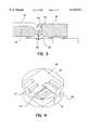
- FIG. 3is a side view illustration of the alignment device in accordance with the present invention.
- FIG. 4is an illustration of the natural crystal planes of III-V semiconductor substrates
- FIG. 5ais a side view illustration of the lapping and polishing of the substrate in accordance with the present invention.
- FIG. 5bis a side view illustration of the substrate of FIG. 5a following the lapping and polishing steps;
- FIG. 5cis a side view illustration of the substrate coated with a layer of photoresist material to begin the formation of a reflective surface through photolithography steps in accordance with the present invention
- FIG. 5dis a side view illustration of the substrate wafer which includes a layer of photoresist material on a surface of the substrate wafer and the layer of photoresist material is exposed by an ultra-violet light source through a mask to later form a reflective mirror in accordance with the present invention
- FIG. 5eis a side view illustration of the substrate wafer and a photoresist mask formed on the surface of the substrate following the exposure of the substrate wafer to the ultra-violet light source in accordance with the present invention
- FIG. 5fis a cross-sectional side view illustration of the preferentially etched surface of the substrate wafer where a flat reflective mirror is formed in accordance with the present invention
- FIG. 5gis a top view of the preferentially etched surface of the substrate wafer where a flat reflective mirror is formed in accordance with the present invention.
- FIG. 5his a cross-sectional side view illustration of the substrate of FIG. 5f where the photoresist has been removed from the surface of the substrate.
- FIG. 5iis a cross-sectional side view illustration of the substrate wafer coated with a layer of photoresist material to begin the formation of a groove through photolithography steps on the surface opposite where the flat reflective mirror is formed in accordance with the present invention
- FIG. 5jis a side view illustration of the substrate wafer which includes a layer of photoresist material on a surface of the substrate wafer and the layer of photoresist material is exposed by an ultra-violet light source through a mask to later form a groove in accordance with the present invention
- FIG. 5kis a top view illustration of the substrate wafer and a photoresist mask formed on the surface of the substrate following the exposure of the substrate wafer to the ultra-violet light source in accordance with the present invention
- FIG. 5lis a top view illustration of the substrate wafer with an etched groove intersecting the plane of the etched flat reflective mirror in accordance with the present invention
- FIG. 5mis a side view illustration of the substrate wafer with an etched groove intersecting the plane of the etched flat reflective mirror in accordance with the present invention
- FIG. 5nis an illustration of the substrate wafer metallization process in accordance with the present invention.
- FIG. 6ais a side view illustration of the substrate coated with a layer of photoresist material to begin the formation of a lens through photolithography steps in accordance with the present invention
- FIG. 6bis a side view illustration of the substrate wafer which includes a layer of photoresist material on a surface of the substrate wafer and the layer of photoresist material is exposed by an ultra-violet light source through a mask to later form a lens in accordance with the present invention
- FIG. 6cis a side view illustration of the substrate wafer and a photoresist mask formed on the surface of the substrate wafer after the exposure of the substrate wafer to the ultra-violet light source and photolithographic development in accordance with the present invention
- FIG. 6dis a cross-sectional side view illustration of the preferentially etched surface of the substrate wafer where a lens is formed in accordance with the present invention
- FIG. 6eis a cross-sectional side view illustration of the substrate wafer of FIG. 6d where the photoresist has been removed from the surface of the substrate.
- FIG. 6fis a side view illustration of the substrate wafer where the lens has been polished and coated with antireflectivity coating in accordance with the present invention.
- FIG. 7is an illustration of the alignment device in accordance with the present invention.
- the present inventionrelates to a III-V semiconductor monolithic optical alignment device and a method for producing the same for coupling optical energy between optical devices.
- the alignment devicewhich is a monolithic assembly, can accurately align optical fibers, waveguides or modulators, redirect and focus optical energy to and from optical devices using a reflective surface and a micro-optical lens.
- the construction of the alignment deviceis accomplished by exploiting the anisotropic etch characteristics of III-V semiconductors. Etching in one direction creates a natural channel for precise fiber positioning; etching in another direction, which is orthogonal, creates a reflective surface at one end of the fiber channel for redirecting optical energy, and finally a micro-optical lens is non-selectively etched for focusing optical energy.
- the ability to form a monolithic compact and simple optical coupling system for micro-optical deviceshas several advantages.
- the alignment devicecan be made of the same semiconductor material as the device, there is better thermal expansion match between the microbench and the micro-optical device. Having the best thermal expansion match is important for stability where differences in thermal expansion coefficients can cause optical misalignments during temperature changes.
- efficient couplingcan be accomplished between a fiber, reflective surface, lens, and a device without the use of complex coupling and alignment schemes which require many components and complicated assembly processes.
- the present inventionrelates to an improvement in the coupling of optical energy between optical devices.
- Present optical systemsuse a variety of coupling schemes which can be very complex and unreliable.
- a reflective mirror, micro-optical lens, and fiber groovecan be formed monolithically from the same semiconductor material to form an optical alignment device.
- III-V semiconductorssuch as indium phosphide (InP), gallium arsenide (GaAs), indium arsenide (InAs), and gallium phosphide (GaP).
- InPindium phosphide
- GaAsgallium arsenide
- InAsindium arsenide
- GaPgallium phosphide
- the present inventionrelates to an optical alignment device and, more particularly, to an optical alignment device which includes a III-V semiconductor substrate 36, such as indium phosphide (InP), a fiber groove 38, a lens 39, and a reflective mirror 40, as illustrated in FIG. 3.
- a III-V semiconductor substrate 36such as indium phosphide (InP)
- the fiber groove 38provides a natural channel for precise optical fiber positioning where optical energy 42 is emitted from an optical fiber 44 and redirected at the reflective mirror 40 and focused at the lens 39 for collection at an optical detector device 46.
- the principles of the present inventionare also applicable for coupling optical energy from a waveguide to an optical device.
- the reflective mirrorcan be used for redirecting and focusing the diverging output of optical energy from an emitter or waveguide, or it can be used for collecting the optical energy coming to the input of a waveguide or detector.
- FIG. 4For illustration, a method for producing the monolithic optical alignment device is described and illustrated further in FIG. 4, FIGS. 5a through 5n, and FIGS. 6a through 6f with a substrate wafer 48, a groove 82, a lens 116, and a reflective mirror 66.
- the first steps of the alignment device fabricationrelate to the formation of a groove and a reflective mirror from semiconductor material by standard photolithography processes.
- the construction of the alignment deviceis accomplished by exploiting the anisotropic etch characteristics of III-V semiconductors.
- the unique crystal plane properties, as illustrated in FIG. 4, of III-V semiconductor materialallow for the preferential etching of reflective surfaces in one (111) crystal plane 47 of a substrate, etching a lens on a (001) crystal plane 34 of the substrate wafer, and etching an intersecting groove on an (100) crystal plane 35 of the substrate wafer.
- the first step of the alignment device fabrication processinvolves lapping the entire first surface 54 of an indium phosphide (InP) substrate wafer 48 and polishing the entire first surface 54 to a thickness of from approximately 135 to 175 microns, as illustrated in FIGS. 5a and 5b.
- the lapping and polishing stepsare performed to provide the substrate wafer 48 with a desired thickness and are performed while the substrate wafer 48 is secured using wax 52 on a carrier S0.
- the first step of the reflective mirror fabrication processis coating a layer of photoresist material 56 over the entire first surface 54 of the indium phosphide (InP) substrate wafer 48.
- the preferred photoresist material 56is 2-ethoxpyethylacetate (60%) and n-butyl acetate (5%) in xylene and hexamethyldisilozane (HDMS), and is preferred for its suitability for use with a variety of etching techniques.
- the indium phosphide substrate wafer 48is chosen for its etching characteristics and its ability to form a high refractive lens index with few aberrations.
- the substrate wafer 48may be any III-V semiconductor material and may include gallium arsenide (GaAs), indium arsenide (InAs), and gallium phosphide (GaP).
- GaAsgallium arsenide
- InAsindium arsenide
- GaPgallium phosphide
- the photoresist coating material 56may include 2-ethoxyethylacetate+n-butyl acetate in xylene solvent, 2-ethoxyethylacetate+n-butyl acetate in xylene and silicon dioxide (SiO 2 ), 2-ethoxyethylacetate+n-butyl acetate in xylene and silicon nitride (Si 3 N 4 ), silicon dioxide (SiO 2 ) and complex silicon nitride (Si x N y ), or aluminum oxide (Al 2 O 3 ).
- the substrate wafer 48is soft baked at a temperature of from approximately 100° C. to 150° C. and for a period of approximately 45 minutes to remove any solvent from the photoresist material 56.
- a mask 58is used to transfer a reflective mirror pattern 60 from the mask 58 to the substrate wafer 48.
- the mask 58is aligned to the substrate wafer 48 along the (111) crystal plane and the layer of photoresist material 56 is exposed to an ultra violet UV light source 62 through the mask 58 to transfer the reflective mirror pattern 60 to the substrate wafer 48.
- the layer of photoresist material 56 of FIG. 5dis developed to form a photoresist mask 64 on the first surface 54 of the substrate wafer 48 and the photoresist mask 64 is rebaked at approximately 150° C. for approximately one hour.
- the development of photoresist materialis a standard step in photolithography processing.
- the substrate wafer 48is preferentially etched in the areas not protected by the photoresist mask 64, as illustrated in FIGS. 5f and 5g, to form a flat reflective mirror 66.
- This preferential etching stepis done by a wet-chemical etch process where the substrate 48 is etched in an orthogonal direction on the (111) crystal plane 47 illustrated in FIG. 4.
- the unique crystal plane properties of III-V semiconductor materialallows for the preferential etching of flat angled reflective surfaces of between 36 and 53 degrees, as illustrated in the preferred embodiment.
- 5fis wet-chemically etched in a deionized water:potassium dichromate:acetic acid:hydrobromic acid (H 2 O:K 2 Cr 2 O 7 :H 3 CCOOH:HBr), 450 ml:66 g: 100 ml:300 ml solution at a temperature below zero degree C.
- Alternative wet-chemical etch solutionsmay include bromine:methanol (Br 2 :H 3 COH), bromine:isopropanol (Br 2 :H 5 C 2 OH), deionized water:hydrobromic acid:acetic acid (H 2 O:HBr:H 3 CCOOH), deionized water:potassium dichromate:sulfuric acid:hydrochloric acid (H 2 O:K 2 Cr 2 O 7 :H 2 SO 4 :HCl), phosphoric acid:hydrochloric acid (H 3 PO 4 :HCl), phosphoric acid:hydrochloric acid:deionized water (H 3 PO 4 :HCl:H 2 O), phosphoric acid:hydrochloric acid:hydrogen peroxide (H 3 PO 4 :HCl:H 2 O 2 ), iron chloride:hydrochloric acid (FeCl 3 :HCl) under illumination, potassium periodide:hydrochloric acid (KIO 3 :HCl), hydrochloric acid:acetic
- the photoresist mask 64is removed from the surface 54 of the substrate wafer 48, as illustrated in FIG. 5h.
- the surface 54is cleaned using acetone.
- the acetoneis removed from the surface 54 of the substrate wafer 48 with isopropanol and the isopropanol is removed using deionized water.
- oxidesare removed from the surface 54 using potassium hydroxide (KOH) and etch residue is removed from the surface 54 using a solution of sulfuric acid:hydrogen perodixe:deionized water (H 2 SO 4 :H 2 O 2 :H 2 O).
- the monolithic integration of a reflective surface and a grooveis significant.
- Monolithic integrationallows for more reliable and less complex optical alignment between optical devices.
- a grooveis formed on the surface of the substrate wafer where the reflective mirror has been formed.
- the first steps in the fabrication of the grooveare photolithography steps, as shown in FIG. 5i.
- the first stepincludes coating a layer of photoresist material 72 on the surface 54 of the substrate wafer 48 where the flat reflective mirror 66 has previously been formed.
- the preferred photoresist material 72is 2-ethoxyethylacetate+n-butyl acetate in xylene.
- the substrate wafer 48is soft baked at a temperature of from approximately 100° C. to 150° C. for a period of approximately 45 minutes to remove solvents from the photoresist material 72.
- a mask 74is used to transfer a groove pattern 76 to the substrate wafer 48.
- the mask 74is selectively aligned to the substrate wafer 48 along the (100) crystal plane.
- the layer of photoresist material 72is exposed with an ultra-violet light source 78 through the mask 74.
- the layer of photoresist material 72is developed creating a photoresist mask 80 on the surface 54 of the substrate wafer 48 and the photoresist mask 80 is rebaked at approximately 150° C. for approximately one hour, as shown in FIG. 5k.
- the surface 54 of the substrate wafer 48 containing the photoresist mask 80is wet-chemically etched in the areas not protected by the photoresist mask 80 to form the groove 82, as shown in FIGS. 5l and 5m.
- the groove 82is etched on the (100) crystal plane 35, shown in FIG. 4, of the substrate wafer 48 in an orthogonal direction such that the end 84 of the groove 82 intersects the plane of the flat reflective mirror 66.
- the groove 82is formed in a semi-circular shape, as shown in FIG. 5l.
- the semi-circular shape of the groove 82allows for increased stability during thermal expansion of the microbench system because the semi-circular groove 82 allows more surface area contact with round optical fibers than equivalent v-groove structures.
- the photoresist mask 80is removed from the surface 54 of the substrate wafer 48 and the surface 54 of the substrate wafer 48 is cleaned, using the same steps described in the formation of the flat reflective mirror.
- a micro-optical lensis formed on the substrate wafer 48 opposite the surface 54 where the groove 82 and flat reflective mirror 66 have been formed. More specifically and with reference to the drawings, the first steps of the micro-optical lens fabrication, as illustrated in FIGS. 6a through 6f, relate to the formation of a micro-optical lens by photolithography processes.
- the first step of the lens fabrication process, as illustrated in FIG. 6a,is coating a layer of photoresist material 102 over an entire surface 70 of the substrate wafer 48.
- the preferred photoresist material 102is 2-ethoxpyethylacetate (60%) and n-butyl acetate (5%) in xylene and hexamethyldisilozane (HDMS).
- the indium phosphide substrate wafer 48is chosen for its etching characteristics and its ability to form a high refractive index lens with low aberrations.
- the photoresist coating material 102may include 2-ethoxyethylacetate+n-butyl acetate in xylene solvent, 2-ethoxyethylacetate+n-butyl acetate in xylene and silicon dioxide (SiO 2 ) precoated, 2-ethoxyethylacetate+n-butyl acetate in xylene and silicon nitride (Si 3 N 4 ) precoated, silicon dioxide (SiO 2 ) and complex silicon nitride (Si x N y ), or aluminum oxide (Al 2 O 3 ) precoated.
- the substrate wafer 48After coating the layer of photoresist material 102 over the surface 70 of the substrate wafer 48, the substrate wafer 48 is soft baked at a temperature of from approximately 100° C. to 150° C. and for a period of approximately 45 minutes to remove any solvent from the photoresist material 102.
- a mask 106is used to transfer a lens pattern 104 from the mask 106 to the substrate wafer 48.
- Lens patternsare chosen based on the type of lens required for a particular optical application. For the purposes of the preferred embodiment a semi-spherical lens is chosen.
- the type of lens formed on a semiconductor substrate wafercan be aspherical, semi-cylindrical, gausian-cylindrical, binary, Fresnell, refractive, or diffractive as dictated by the mask pattern.
- the mask 106is aligned to the substrate wafer 48 so that the lens formed by subsequent etching steps and the reflective mirror 66 are optically aligned.
- the mask 106is aligned along a (110) crystal plane 33 (see FIG. 4) of the substrate wafer 48 using an infra-red camera.
- the layer of photoresist material 102is then exposed to an ultra violet UV light source 108 through the mask 106 to transfer the lens pattern 104 to the substrate wafer 48.
- the layer of photoresist material 102 of FIG. 6ais developed to form a photoresist mask 110 on the surface 70 of the substrate wafer 48 and the photoresist mask 110 is rebaked at approximately 150° C. for approximately one hour.
- the development of photoresist materialis a standard step in photolithography processing.
- the substrate wafer 48is non-selectively etched in the areas surrounding the photoresist mask 110, as illustrated in FIG. 6d.
- the oxide or nitridemust be removed before the non-selective etching is performed.
- the non-selective etching stepis done to begin the formation of a lens and can be accomplished by a wet-chemical etch process on the (001) crystal plane 34 (see FIG. 4) of the substrate wafer 48.
- 6dis wet-chemically etched in a deionized water:potassium dichromate:acetic acid:hydrobromic acid (H 2 O:K 2 Cr 2 O 7 :H 3 CCOOH:HBr), 450 ml:66 g: 100 ml:300 ml solution at a temperature of from 40° C. to 60° C.
- alternative wet-chemical etch solutionscan include bromine:methanol (Br 2 :H 3 COH), bromine:isopropanol (Br 2 :H 5 C 2 OH), deionized water:hydrobromic acid:acetic acid (H 2 O:HBr:H 3 CCOOH), deionized water:potassium dichromate:sulfuric acid:hydrochloric acid (H 2 O:K 2 Cr 2 O 7 :H 2 SO 4 :HCl), phosphoric acid:hydrochloric acid (H 3 PO 4 :HCl), phosphoric acid:hydrochloric acid:deionized water (H 3 PO 4 :HCl:H 2 O), phosphoric acid:hydrochloric acid:hydrogen peroxide (H 3 PO 4 :HCl:H 2 O 2 ), iron chloride:hydrochloric acid (FeCl 3 :HCl) under illumination, potassium periodide:hydrochloric acid (KIO 3 :HCl), hydro
- the photoresist mask 110is removed from the surface 70 of the substrate wafer 48, as illustrated in FIG. 6e.
- the surface 70 of the substrate wafer 48is cleaned using acetone.
- the acetoneis removed from the surface 70 of the substrate wafer 48 with isopropanol and the isopropanol is removed using deionized water.
- the photoresistcan also be removed using photoresist stripper, potassium hydroxide, or other equivalent alkaline chemicals followed by a deionized water rinse.
- oxidesare removed from the surface 70 using potassium hydroxide (KOH) and etch residue is removed from the surface 70 using a solution of sulfuric acid:hydrogen perodixe:deionized water (H 2 SO 4 :H 2 O 2 :H 2 O).
- KOHpotassium hydroxide
- the lensis polished by etching the entire surface 70 of the substrate wafer 48, where an etched peak 112 on the surface 70 of the substrate wafer 48 has been formed.
- the same wet-chemical etching solution described in FIG. 6dis used here to polish the lens by smoothing the surface of the etched peak 112.
- Etching the entire surface 70 of the substrate wafer 48 to polish the lensrequires that the etching be done at a lower temperature, preferably 30° C. to 40° C.
- the result of this low temperature etchis a lens 114 formed on the surface 70 of the substrate wafer 48.
- the lens 114is coated with antireflectivity coating 116 using an electron beam (e-beam) evaporation process.
- e-beamelectron beam
- e-beam evaporation processuses an e-beam evaporation process to apply the antireflectivity coating
- alternative processeslike sputtering or chemical vapor deposition (CVD) can also be used.
- a crystal mixture of antireflectivity (AR) coatingwhich contains magnesium flouride (MgF), aluminum oxide (Al 2 O 3 ), hafnium flouride (HfF), silicon dioxide (SiO 2 ), and silicon nitride (Si 3 N 4 ) is deposited over the entire surface 70 of the substrate wafer 48 containing the lens 114.
- the entire substrate 48is metallized, except in the area of the lens 66, by first evaporating 92 a layer 86 of titanium (Ti) over the substrate wafer 48, evaporating 92 a layer of platinum (Pt) 88 over the layer 86 of titanium, evaporating 92 a layer 90 of gold (Au) over the layer 88 of platinum, and applying a standard alloy treatment to the metal layers to bond the layers for better adhesion, as illustrated in FIG. 5n.
- Tititanium
- Ptplatinum
- Augold
- an optical fiber 92 and the substrate wafer 48are secured using eutectic bonds 100.
- the optical fiber 92is secured in the groove 82 and the substrate wafer 48 is mounted to optical devices 94.
- An optical signal 96is emitted from the optical fiber 92 and is reflected at the flat reflective mirror 66 and focused through the lens 116 to a target area 98.
Landscapes
- Physics & Mathematics (AREA)
- General Physics & Mathematics (AREA)
- Optics & Photonics (AREA)
- Optical Couplings Of Light Guides (AREA)
- Light Receiving Elements (AREA)
- Semiconductor Lasers (AREA)
- Led Devices (AREA)
Abstract
Description
Claims (13)
Priority Applications (2)
| Application Number | Priority Date | Filing Date | Title |
|---|---|---|---|
| US09/074,187US6115521A (en) | 1998-05-07 | 1998-05-07 | Fiber/waveguide-mirror-lens alignment device |
| JP12770399AJP3137958B2 (en) | 1998-05-07 | 1999-05-07 | Fiber / waveguide-mirror-lens alignment device |
Applications Claiming Priority (1)
| Application Number | Priority Date | Filing Date | Title |
|---|---|---|---|
| US09/074,187US6115521A (en) | 1998-05-07 | 1998-05-07 | Fiber/waveguide-mirror-lens alignment device |
Publications (1)
| Publication Number | Publication Date |
|---|---|
| US6115521Atrue US6115521A (en) | 2000-09-05 |
Family
ID=22118199
Family Applications (1)
| Application Number | Title | Priority Date | Filing Date |
|---|---|---|---|
| US09/074,187Expired - LifetimeUS6115521A (en) | 1998-05-07 | 1998-05-07 | Fiber/waveguide-mirror-lens alignment device |
Country Status (2)
| Country | Link |
|---|---|
| US (1) | US6115521A (en) |
| JP (1) | JP3137958B2 (en) |
Cited By (55)
| Publication number | Priority date | Publication date | Assignee | Title |
|---|---|---|---|---|
| US6215925B1 (en)* | 1996-05-31 | 2001-04-10 | Nec Corporation | Optical combination of photoreceptor and optical fiber |
| US6236788B1 (en)* | 1998-10-01 | 2001-05-22 | Daimlerchrysler Ag | Arrangement for aligning optical components |
| DE10065197A1 (en)* | 2000-12-20 | 2002-07-11 | Euromicron Werkzeuge Gmbh | imaging optics |
| US20020154866A1 (en)* | 2001-04-02 | 2002-10-24 | Craig Tombling | Alignment of optical fibres with an optical device |
| US6477302B2 (en)* | 2000-01-12 | 2002-11-05 | Sumitomo Electric Industries, Ltd. | Microbench and producing method therefor, and optical semiconductor module using same |
| WO2003005090A1 (en)* | 2001-06-30 | 2003-01-16 | Mergeoptics Gmbh | Device for positioning an optical fibre |
| US6580858B2 (en)* | 2001-04-30 | 2003-06-17 | Xerox Corporation | Micro-opto-electro-mechanical system (MOEMS) |
| GB2385197A (en)* | 2002-02-07 | 2003-08-13 | Denselight Semiconductors Pte | Semiconductor laser with monitor photodetector arrangement |
| US20030231828A1 (en)* | 2002-06-13 | 2003-12-18 | Brock John C. | Integrated aspheric optical coupler for RF planarized automatic photonics packaging |
| US6704070B2 (en)* | 2000-06-29 | 2004-03-09 | Hitachi, Ltd. | Method for manufacturing a light guide plate |
| US20040114881A1 (en)* | 2002-12-12 | 2004-06-17 | Wilson Robert Edward | Optical apparatus and method for coupling output light from a light source to an optical waveguide |
| EP1447696A1 (en)* | 2003-02-04 | 2004-08-18 | Infineon Technologies AG | Modular system of optoelectronic components and optoelectronic components to be used in the system |
| KR100478796B1 (en)* | 2001-12-04 | 2005-03-25 | 마쯔시다덴기산교 가부시키가이샤 | Optical package substrate and optical device |
| US20050190682A1 (en)* | 2004-02-26 | 2005-09-01 | Seagate Technology Llc | Head with optical bench for use in data storage devices |
| EP1480063A3 (en)* | 2003-05-19 | 2005-09-07 | Infineon Technologies AG | Opto-electronic modules for transmission and/or reception |
| US20060005460A1 (en)* | 2004-06-28 | 2006-01-12 | Bittrick Mark E | Fish dimension recording towel |
| US20060022289A1 (en)* | 2002-04-16 | 2006-02-02 | Xloom Photonics, Ltd. | Electro-optical circuitry having integrated connector and methods for the production thereof |
| US20060067607A1 (en)* | 2004-09-30 | 2006-03-30 | Stmicroelectronics, Inc. | Method and system for vertical optical coupling on semiconductor substrate |
| US20060141806A1 (en)* | 2004-06-18 | 2006-06-29 | Carlo Waldfried | Apparatus and process for treating dielectric materials |
| US20060145279A1 (en)* | 2002-04-16 | 2006-07-06 | Xloom Photonics, Ltd. | Electro-optic integrated circuits with connectors and methods for the production thereof |
| DE102005008885A1 (en)* | 2005-02-26 | 2006-09-07 | Sick Ag | Optical interconnection unit for light curtain or light barrier, has printed circuit board comprising conducting paths, and optical lens integrated in board, where board is rigid and lens is attached to receiving and/or transmitting unit |
| US20060274323A1 (en)* | 2005-03-16 | 2006-12-07 | Gibler William N | High intensity fabry-perot sensor |
| US20070077008A1 (en)* | 2005-09-30 | 2007-04-05 | Doosan Corporation | Optical interconnection module and method of manufacturing the same |
| EP1561139A4 (en)* | 2002-11-12 | 2007-12-12 | Xponent Photonics Inc | Optical component for free-space optical propagation between waveguides |
| US20080174781A1 (en)* | 2006-04-18 | 2008-07-24 | Berthold John W | Fiber optic seismic sensor based on MEMS cantilever |
| US20080206919A1 (en)* | 2004-09-30 | 2008-08-28 | Stmicroelectronics, Inc. | Method of manufacture of a microlens structure for opto-electric semiconductor device |
| US20080226221A1 (en)* | 2007-03-13 | 2008-09-18 | Serge Bidnyk | Integrated reflector for planar lightwave circuits |
| US20080226443A1 (en)* | 2007-03-08 | 2008-09-18 | Davidson Instruments, Inc. | Apparatus and methods for monitoring combustion dynamics in a gas turbine engine |
| US20090034085A1 (en)* | 2003-10-15 | 2009-02-05 | Xloom Communications, Ltd. | Electro-optical circuitry having integrated connector and methods for the production thereof |
| US20090093137A1 (en)* | 2007-10-08 | 2009-04-09 | Xloom Communications, (Israel) Ltd. | Optical communications module |
| US20090277228A1 (en)* | 2002-02-28 | 2009-11-12 | Matsushita Electric Industrial Co., Ltd. | Three-dimensional optical waveguide, method of manufacturing same, optical module, and optical transmission system |
| US7639368B2 (en) | 2005-09-13 | 2009-12-29 | Halliburton Energy Services, Inc. | Tracking algorithm for linear array signal processor for Fabry-Perot cross-correlation pattern and method of using same |
| US7743661B2 (en) | 2006-04-26 | 2010-06-29 | Halliburton Energy Services, Inc. | Fiber optic MEMS seismic sensor with mass supported by hinged beams |
| US7787128B2 (en) | 2007-01-24 | 2010-08-31 | Halliburton Energy Services, Inc. | Transducer for measuring environmental parameters |
| US7835598B2 (en) | 2004-12-21 | 2010-11-16 | Halliburton Energy Services, Inc. | Multi-channel array processor |
| US7864329B2 (en) | 2004-12-21 | 2011-01-04 | Halliburton Energy Services, Inc. | Fiber optic sensor system having circulators, Bragg gratings and couplers |
| US7940400B2 (en) | 2004-04-15 | 2011-05-10 | Halliburton Energy Services Inc. | Method and apparatus for continuous readout of fabry-perot fiber optic sensor |
| US20110262081A1 (en)* | 2010-04-23 | 2011-10-27 | Ruprecht-Karls-Universitat Heidelberg | Optical connectors and a method of production thereof |
| US8115937B2 (en) | 2006-08-16 | 2012-02-14 | Davidson Instruments | Methods and apparatus for measuring multiple Fabry-Perot gaps |
| WO2012166286A1 (en)* | 2011-05-27 | 2012-12-06 | Google Inc. | Image relay waveguide and method of producing same |
| US20130177274A1 (en)* | 2012-01-10 | 2013-07-11 | Invensas Corporation | Structures formed using monocrystalline silicon and/or other materials for optical and other applications |
| US20130177281A1 (en)* | 2012-01-10 | 2013-07-11 | Invensas Corporation | Optical interposer |
| WO2014018043A1 (en)* | 2012-07-26 | 2014-01-30 | Hewlett-Packard Development Company, L.P. | Optical engine |
| US9052464B1 (en)* | 2013-01-18 | 2015-06-09 | Kotura, Inc. | Transfer of light signals between optical devices |
| US9122027B2 (en) | 2012-09-28 | 2015-09-01 | International Business Machines Corporation | High-precision passive alignment of optical components with optical waveguides using a common adapter |
| CN105242360A (en)* | 2006-12-22 | 2016-01-13 | 思科技术公司 | Dual-lensed unitary optical receiver assembly |
| US9274293B2 (en) | 2012-09-28 | 2016-03-01 | International Business Machines Corporation | Arrangement of photonic chip and optical adaptor for coupling optical signals |
| WO2016199985A1 (en)* | 2015-06-11 | 2016-12-15 | 주식회사 지피 | Multichannel optical receiver module and optical alignment method of multichannel optical receiver module |
| US20170068057A1 (en)* | 2015-09-04 | 2017-03-09 | Ccs Technology, Inc. | Fiber coupling device for coupling of at least one optical fiber |
| US10175432B2 (en)* | 2014-11-18 | 2019-01-08 | Konica Minolta, Inc. | Optical path change element and optical coupling device |
| CN110208908A (en)* | 2019-05-24 | 2019-09-06 | 宁波东立创芯光电科技有限公司 | A kind of two-dimension focusing deviation mirror on optical waveguide loop |
| US10488595B2 (en) | 2016-08-12 | 2019-11-26 | Sicoya Gmbh | Photonic component and method for producing same |
| US11075500B2 (en)* | 2012-11-30 | 2021-07-27 | Lumentum Japan, Inc. | Optical device having a substrate and a laser unit that emits light into the substrate |
| US11163122B2 (en)* | 2018-06-29 | 2021-11-02 | 3M Innovative Properties Company | Optical ferrule |
| US11693193B2 (en) | 2018-06-29 | 2023-07-04 | 3M Innovative Properties Company | Optical ferrule having compound stops |
Families Citing this family (22)
| Publication number | Priority date | Publication date | Assignee | Title |
|---|---|---|---|---|
| JP2001174264A (en)* | 1999-12-21 | 2001-06-29 | Murata Mfg Co Ltd | Resonant element and vibration adjustment method thereof |
| JP2001189468A (en)* | 2000-01-05 | 2001-07-10 | Sumitomo Electric Ind Ltd | Optical module |
| JP4360651B2 (en)* | 2006-08-14 | 2009-11-11 | 古河電気工業株式会社 | Optical module and manufacturing method thereof |
| CA2700108C (en) | 2007-09-19 | 2015-10-13 | Mitsubishi Cable Industries, Ltd. | Optical fiber structure, system for fabricating the same, and block-like chip for use therein |
| JP2009198908A (en)* | 2008-02-22 | 2009-09-03 | Nippon Electric Glass Co Ltd | Lens component for optical communication |
| US8818145B2 (en)* | 2011-08-03 | 2014-08-26 | Tyco Electronics Corporation | Optical interposer with transparent substrate |
| EP3140838B1 (en) | 2014-05-05 | 2021-08-25 | 3D Glass Solutions, Inc. | Inductive device in a photo-definable glass structure |
| KR20180134868A (en) | 2016-02-25 | 2018-12-19 | 3디 글래스 솔루션즈 인코포레이티드 | A photoactive substrate for fabricating 3D capacitors and capacitor arrays |
| US12165809B2 (en) | 2016-02-25 | 2024-12-10 | 3D Glass Solutions, Inc. | 3D capacitor and capacitor array fabricating photoactive substrates |
| US11161773B2 (en)* | 2016-04-08 | 2021-11-02 | 3D Glass Solutions, Inc. | Methods of fabricating photosensitive substrates suitable for optical coupler |
| KR102273624B1 (en) | 2017-04-28 | 2021-07-07 | 3디 글래스 솔루션즈 인코포레이티드 | Rf Circulator |
| KR102418671B1 (en) | 2017-07-07 | 2022-07-12 | 3디 글래스 솔루션즈 인코포레이티드 | 2d and 3d rf lumped element devices for rf system in a package photoactive glass substrates |
| JP7008824B2 (en) | 2017-12-15 | 2022-01-25 | スリーディー グラス ソリューションズ,インク | Connection transmission line resonant RF filter |
| EP3735743A4 (en) | 2018-01-04 | 2021-03-03 | 3D Glass Solutions, Inc. | Impedance matching conductive structure for high efficiency rf circuits |
| EP3643148A4 (en) | 2018-04-10 | 2021-03-31 | 3D Glass Solutions, Inc. | INTEGRATED RF POWER CONDITIONING CAPACITOR |
| US10903545B2 (en) | 2018-05-29 | 2021-01-26 | 3D Glass Solutions, Inc. | Method of making a mechanically stabilized radio frequency transmission line device |
| US11139582B2 (en) | 2018-09-17 | 2021-10-05 | 3D Glass Solutions, Inc. | High efficiency compact slotted antenna with a ground plane |
| AU2019416327B2 (en) | 2018-12-28 | 2021-12-09 | 3D Glass Solutions, Inc. | Annular capacitor RF, microwave and MM wave systems |
| AU2019416325A1 (en) | 2018-12-28 | 2021-02-04 | 3D Glass Solutions, Inc. | Heterogenous integration for RF, microwave and mm wave systems in photoactive glass substrates |
| JP7140435B2 (en) | 2019-04-05 | 2022-09-21 | スリーディー グラス ソリューションズ,インク | Glass-based empty substrate integrated waveguide device |
| KR102601781B1 (en) | 2019-04-18 | 2023-11-14 | 3디 글래스 솔루션즈 인코포레이티드 | High efficiency die dicing and release |
| KR20220164800A (en) | 2020-04-17 | 2022-12-13 | 3디 글래스 솔루션즈 인코포레이티드 | broadband inductor |
Citations (13)
| Publication number | Priority date | Publication date | Assignee | Title |
|---|---|---|---|---|
| US4433898A (en)* | 1980-12-22 | 1984-02-28 | National Semiconductor Corporation | Fiber optic assembly for coupling an optical fiber and a light source |
| US4653847A (en)* | 1981-02-23 | 1987-03-31 | Motorola, Inc. | Fiber optics semiconductor package |
| US4875750A (en)* | 1987-02-25 | 1989-10-24 | Siemens Aktiengesellschaft | Optoelectronic coupling element and method for its manufacture |
| US5071213A (en)* | 1990-10-31 | 1991-12-10 | The Boeing Company | Optical coupler and method of making optical coupler |
| US5073003A (en)* | 1988-12-23 | 1991-12-17 | At&T Bell Laboratories | Optoelectronic device package method and apparatus |
| US5247597A (en)* | 1992-03-25 | 1993-09-21 | International Business Machines Corporation | Optical fiber alignment |
| US5343546A (en)* | 1993-03-26 | 1994-08-30 | Polaroid Corporation | Microbench |
| US5346583A (en)* | 1993-09-02 | 1994-09-13 | At&T Bell Laboratories | Optical fiber alignment techniques |
| US5600741A (en)* | 1994-05-11 | 1997-02-04 | Ant Nachrichtentechnik Gmbh | Arrangement for coupling optoelectronic components and optical waveguides to one another |
| US5627931A (en)* | 1996-05-28 | 1997-05-06 | Motorola | Optoelectronic transducer |
| US5774609A (en)* | 1996-01-26 | 1998-06-30 | Telefonaktiebolaget Lm Ericsson | Method and arrangement for coupling a wave guide to a component |
| US5898803A (en)* | 1996-04-27 | 1999-04-27 | Robert Bosch Gmbh | Optical, beam-splitting component and a method for producing a prism carrier plate for such a component |
| US5987202A (en)* | 1995-01-18 | 1999-11-16 | Robert Bosch Gmbh | Arrangement for converting optical signals into electrical signals and method of producing the arrangement |
- 1998
- 1998-05-07USUS09/074,187patent/US6115521A/ennot_activeExpired - Lifetime
- 1999
- 1999-05-07JPJP12770399Apatent/JP3137958B2/ennot_activeExpired - Fee Related
Patent Citations (13)
| Publication number | Priority date | Publication date | Assignee | Title |
|---|---|---|---|---|
| US4433898A (en)* | 1980-12-22 | 1984-02-28 | National Semiconductor Corporation | Fiber optic assembly for coupling an optical fiber and a light source |
| US4653847A (en)* | 1981-02-23 | 1987-03-31 | Motorola, Inc. | Fiber optics semiconductor package |
| US4875750A (en)* | 1987-02-25 | 1989-10-24 | Siemens Aktiengesellschaft | Optoelectronic coupling element and method for its manufacture |
| US5073003A (en)* | 1988-12-23 | 1991-12-17 | At&T Bell Laboratories | Optoelectronic device package method and apparatus |
| US5071213A (en)* | 1990-10-31 | 1991-12-10 | The Boeing Company | Optical coupler and method of making optical coupler |
| US5247597A (en)* | 1992-03-25 | 1993-09-21 | International Business Machines Corporation | Optical fiber alignment |
| US5343546A (en)* | 1993-03-26 | 1994-08-30 | Polaroid Corporation | Microbench |
| US5346583A (en)* | 1993-09-02 | 1994-09-13 | At&T Bell Laboratories | Optical fiber alignment techniques |
| US5600741A (en)* | 1994-05-11 | 1997-02-04 | Ant Nachrichtentechnik Gmbh | Arrangement for coupling optoelectronic components and optical waveguides to one another |
| US5987202A (en)* | 1995-01-18 | 1999-11-16 | Robert Bosch Gmbh | Arrangement for converting optical signals into electrical signals and method of producing the arrangement |
| US5774609A (en)* | 1996-01-26 | 1998-06-30 | Telefonaktiebolaget Lm Ericsson | Method and arrangement for coupling a wave guide to a component |
| US5898803A (en)* | 1996-04-27 | 1999-04-27 | Robert Bosch Gmbh | Optical, beam-splitting component and a method for producing a prism carrier plate for such a component |
| US5627931A (en)* | 1996-05-28 | 1997-05-06 | Motorola | Optoelectronic transducer |
Non-Patent Citations (2)
| Title |
|---|
| Y. Oikawa, H. Kuwatsuka, T. Tamamoto, T. Ihara, H. Hamano, and T. Minami "Packaging Technology for a 10-Gb/s Photoreceiver Module", Journal of Lightwave Technology, vol. 12, No. 2, Feb. 1992, pp. 343-352. |
| Y. Oikawa, H. Kuwatsuka, T. Tamamoto, T. Ihara, H. Hamano, and T. Minami Packaging Technology for a 10 Gb/s Photoreceiver Module , Journal of Lightwave Technology, vol. 12, No. 2, Feb. 1992, pp. 343 352.* |
Cited By (91)
| Publication number | Priority date | Publication date | Assignee | Title |
|---|---|---|---|---|
| US6215925B1 (en)* | 1996-05-31 | 2001-04-10 | Nec Corporation | Optical combination of photoreceptor and optical fiber |
| US6236788B1 (en)* | 1998-10-01 | 2001-05-22 | Daimlerchrysler Ag | Arrangement for aligning optical components |
| US6477302B2 (en)* | 2000-01-12 | 2002-11-05 | Sumitomo Electric Industries, Ltd. | Microbench and producing method therefor, and optical semiconductor module using same |
| US6704070B2 (en)* | 2000-06-29 | 2004-03-09 | Hitachi, Ltd. | Method for manufacturing a light guide plate |
| DE10065197A1 (en)* | 2000-12-20 | 2002-07-11 | Euromicron Werkzeuge Gmbh | imaging optics |
| US20040057028A1 (en)* | 2000-12-20 | 2004-03-25 | Euromicron Werkzeuge Gmbh | Projector lens |
| US6980364B2 (en) | 2000-12-20 | 2005-12-27 | Euromicron Werkzeuge Gmbh | Projector lens |
| US20020154866A1 (en)* | 2001-04-02 | 2002-10-24 | Craig Tombling | Alignment of optical fibres with an optical device |
| US6728450B2 (en)* | 2001-04-02 | 2004-04-27 | Kamelian Limited, A Body Corporate | Alignment of optical fibers with an optical device |
| US6580858B2 (en)* | 2001-04-30 | 2003-06-17 | Xerox Corporation | Micro-opto-electro-mechanical system (MOEMS) |
| WO2003005090A1 (en)* | 2001-06-30 | 2003-01-16 | Mergeoptics Gmbh | Device for positioning an optical fibre |
| KR100478796B1 (en)* | 2001-12-04 | 2005-03-25 | 마쯔시다덴기산교 가부시키가이샤 | Optical package substrate and optical device |
| US6947645B2 (en) | 2001-12-04 | 2005-09-20 | Matsushita Electric Industrial Co., Ltd. | Optical package substrate and optical device |
| GB2385197A (en)* | 2002-02-07 | 2003-08-13 | Denselight Semiconductors Pte | Semiconductor laser with monitor photodetector arrangement |
| US7869671B2 (en)* | 2002-02-28 | 2011-01-11 | Pansonic Corporation | Three-dimensional optical waveguide, method of manufacturing same, optical module, and optical transmission system |
| US20090277228A1 (en)* | 2002-02-28 | 2009-11-12 | Matsushita Electric Industrial Co., Ltd. | Three-dimensional optical waveguide, method of manufacturing same, optical module, and optical transmission system |
| US20060145279A1 (en)* | 2002-04-16 | 2006-07-06 | Xloom Photonics, Ltd. | Electro-optic integrated circuits with connectors and methods for the production thereof |
| US20060022289A1 (en)* | 2002-04-16 | 2006-02-02 | Xloom Photonics, Ltd. | Electro-optical circuitry having integrated connector and methods for the production thereof |
| US20090154873A1 (en)* | 2002-04-16 | 2009-06-18 | Xloom Communications, (Israel) Ltd. | Electro-optic integrated circuits with connectors and methods for the production thereof |
| US20090246905A1 (en)* | 2002-04-16 | 2009-10-01 | Xloom Communications, Inc. | Electro-optic integrated circuits and methods for the production thereof |
| US8043877B2 (en)* | 2002-04-16 | 2011-10-25 | Xloom Communications, Ltd. | Electro-optic integrated circuits and methods for the production thereof |
| US6965714B2 (en) | 2002-06-13 | 2005-11-15 | Northrop Grumman Corporation | Integrated aspheric optical coupler for RF planarized automatic photonics packaging |
| US20030231828A1 (en)* | 2002-06-13 | 2003-12-18 | Brock John C. | Integrated aspheric optical coupler for RF planarized automatic photonics packaging |
| EP1376178A3 (en)* | 2002-06-13 | 2004-08-25 | Northrop Grumman Corporation | Integrated aspheric optical coupler for automatic photonics packaging |
| EP1561139A4 (en)* | 2002-11-12 | 2007-12-12 | Xponent Photonics Inc | Optical component for free-space optical propagation between waveguides |
| US6921214B2 (en)* | 2002-12-12 | 2005-07-26 | Agilent Technologies, Inc. | Optical apparatus and method for coupling output light from a light source to an optical waveguide |
| US20040114881A1 (en)* | 2002-12-12 | 2004-06-17 | Wilson Robert Edward | Optical apparatus and method for coupling output light from a light source to an optical waveguide |
| EP1447696A1 (en)* | 2003-02-04 | 2004-08-18 | Infineon Technologies AG | Modular system of optoelectronic components and optoelectronic components to be used in the system |
| US7182526B1 (en) | 2003-02-04 | 2007-02-27 | Infineon Technologies Ag | Modular system of optoelectronic components, and optoelectronic component for use in such a system |
| EP1480063A3 (en)* | 2003-05-19 | 2005-09-07 | Infineon Technologies AG | Opto-electronic modules for transmission and/or reception |
| US7223023B2 (en) | 2003-05-19 | 2007-05-29 | Infineon Technologies Ag | Optoelectronic transmission and/or reception arrangements |
| US7538358B2 (en) | 2003-10-15 | 2009-05-26 | Xloom Communications, Ltd. | Electro-optical circuitry having integrated connector and methods for the production thereof |
| US20090034085A1 (en)* | 2003-10-15 | 2009-02-05 | Xloom Communications, Ltd. | Electro-optical circuitry having integrated connector and methods for the production thereof |
| US7688689B2 (en) | 2004-02-26 | 2010-03-30 | Seagate Technology Llc | Head with optical bench for use in data storage devices |
| US20050190682A1 (en)* | 2004-02-26 | 2005-09-01 | Seagate Technology Llc | Head with optical bench for use in data storage devices |
| US7940400B2 (en) | 2004-04-15 | 2011-05-10 | Halliburton Energy Services Inc. | Method and apparatus for continuous readout of fabry-perot fiber optic sensor |
| US7709814B2 (en)* | 2004-06-18 | 2010-05-04 | Axcelis Technologies, Inc. | Apparatus and process for treating dielectric materials |
| US20060141806A1 (en)* | 2004-06-18 | 2006-06-29 | Carlo Waldfried | Apparatus and process for treating dielectric materials |
| US20060005460A1 (en)* | 2004-06-28 | 2006-01-12 | Bittrick Mark E | Fish dimension recording towel |
| US20060067607A1 (en)* | 2004-09-30 | 2006-03-30 | Stmicroelectronics, Inc. | Method and system for vertical optical coupling on semiconductor substrate |
| US20080206919A1 (en)* | 2004-09-30 | 2008-08-28 | Stmicroelectronics, Inc. | Method of manufacture of a microlens structure for opto-electric semiconductor device |
| US7389013B2 (en)* | 2004-09-30 | 2008-06-17 | Stmicroelectronics, Inc. | Method and system for vertical optical coupling on semiconductor substrate |
| US7864329B2 (en) | 2004-12-21 | 2011-01-04 | Halliburton Energy Services, Inc. | Fiber optic sensor system having circulators, Bragg gratings and couplers |
| US7835598B2 (en) | 2004-12-21 | 2010-11-16 | Halliburton Energy Services, Inc. | Multi-channel array processor |
| DE102005008885A1 (en)* | 2005-02-26 | 2006-09-07 | Sick Ag | Optical interconnection unit for light curtain or light barrier, has printed circuit board comprising conducting paths, and optical lens integrated in board, where board is rigid and lens is attached to receiving and/or transmitting unit |
| DE102005008885B4 (en)* | 2005-02-26 | 2008-11-27 | Sick Ag | light Curtain |
| US20060274323A1 (en)* | 2005-03-16 | 2006-12-07 | Gibler William N | High intensity fabry-perot sensor |
| US7782465B2 (en) | 2005-03-16 | 2010-08-24 | Halliburton Energy Services, Inc. | High intensity fabry-perot sensor |
| US7639368B2 (en) | 2005-09-13 | 2009-12-29 | Halliburton Energy Services, Inc. | Tracking algorithm for linear array signal processor for Fabry-Perot cross-correlation pattern and method of using same |
| US20070077008A1 (en)* | 2005-09-30 | 2007-04-05 | Doosan Corporation | Optical interconnection module and method of manufacturing the same |
| US7248768B2 (en)* | 2005-09-30 | 2007-07-24 | Doosan Corporation | Optical interconnection module and method of manufacturing the same |
| US20080174781A1 (en)* | 2006-04-18 | 2008-07-24 | Berthold John W | Fiber optic seismic sensor based on MEMS cantilever |
| US7684051B2 (en) | 2006-04-18 | 2010-03-23 | Halliburton Energy Services, Inc. | Fiber optic seismic sensor based on MEMS cantilever |
| US7743661B2 (en) | 2006-04-26 | 2010-06-29 | Halliburton Energy Services, Inc. | Fiber optic MEMS seismic sensor with mass supported by hinged beams |
| US8115937B2 (en) | 2006-08-16 | 2012-02-14 | Davidson Instruments | Methods and apparatus for measuring multiple Fabry-Perot gaps |
| CN105242360A (en)* | 2006-12-22 | 2016-01-13 | 思科技术公司 | Dual-lensed unitary optical receiver assembly |
| US7787128B2 (en) | 2007-01-24 | 2010-08-31 | Halliburton Energy Services, Inc. | Transducer for measuring environmental parameters |
| US20080226443A1 (en)* | 2007-03-08 | 2008-09-18 | Davidson Instruments, Inc. | Apparatus and methods for monitoring combustion dynamics in a gas turbine engine |
| US8125646B2 (en) | 2007-03-08 | 2012-02-28 | Davidson Instruments Inc. | Apparatus and methods for monitoring combustion dynamics in a gas turbine engine |
| US7561764B2 (en) | 2007-03-13 | 2009-07-14 | Enablence Inc. | Integrated reflector for planar lightwave circuits |
| WO2008109982A1 (en)* | 2007-03-13 | 2008-09-18 | Enablence Inc. | Integrated reflector for planar lightwave circuits |
| US20080226221A1 (en)* | 2007-03-13 | 2008-09-18 | Serge Bidnyk | Integrated reflector for planar lightwave circuits |
| US20090093137A1 (en)* | 2007-10-08 | 2009-04-09 | Xloom Communications, (Israel) Ltd. | Optical communications module |
| US8876408B2 (en)* | 2010-04-23 | 2014-11-04 | Ruprecht-Karls-Universität Heidelberg | Optical connectors and a method of production thereof |
| US20110262081A1 (en)* | 2010-04-23 | 2011-10-27 | Ruprecht-Karls-Universitat Heidelberg | Optical connectors and a method of production thereof |
| WO2012166286A1 (en)* | 2011-05-27 | 2012-12-06 | Google Inc. | Image relay waveguide and method of producing same |
| CN103649823A (en)* | 2011-05-27 | 2014-03-19 | 谷歌公司 | Image relay waveguide and method of producing same |
| US8699842B2 (en) | 2011-05-27 | 2014-04-15 | Google Inc. | Image relay waveguide and method of producing same |
| US8757897B2 (en)* | 2012-01-10 | 2014-06-24 | Invensas Corporation | Optical interposer |
| US20130177281A1 (en)* | 2012-01-10 | 2013-07-11 | Invensas Corporation | Optical interposer |
| US9323010B2 (en)* | 2012-01-10 | 2016-04-26 | Invensas Corporation | Structures formed using monocrystalline silicon and/or other materials for optical and other applications |
| US20130177274A1 (en)* | 2012-01-10 | 2013-07-11 | Invensas Corporation | Structures formed using monocrystalline silicon and/or other materials for optical and other applications |
| WO2014018043A1 (en)* | 2012-07-26 | 2014-01-30 | Hewlett-Packard Development Company, L.P. | Optical engine |
| US9520946B2 (en) | 2012-07-26 | 2016-12-13 | Hewlett Packard Enterprise Development Lp | Optical engine |
| US9122028B2 (en) | 2012-09-28 | 2015-09-01 | International Business Machines Corporation | High-precision passive alignment of optical components with optical waveguides using a common adapter |
| US9122027B2 (en) | 2012-09-28 | 2015-09-01 | International Business Machines Corporation | High-precision passive alignment of optical components with optical waveguides using a common adapter |
| US9329348B2 (en) | 2012-09-28 | 2016-05-03 | International Business Machines Corporation | Arrangement of photonic chip and optical adaptor for coupling optical signals |
| US9274293B2 (en) | 2012-09-28 | 2016-03-01 | International Business Machines Corporation | Arrangement of photonic chip and optical adaptor for coupling optical signals |
| US9658414B2 (en) | 2012-09-28 | 2017-05-23 | International Business Machines Corporation | Arrangement of photonic chip and optical adaptor for coupling optical signals |
| US11075500B2 (en)* | 2012-11-30 | 2021-07-27 | Lumentum Japan, Inc. | Optical device having a substrate and a laser unit that emits light into the substrate |
| US9052464B1 (en)* | 2013-01-18 | 2015-06-09 | Kotura, Inc. | Transfer of light signals between optical devices |
| US10175432B2 (en)* | 2014-11-18 | 2019-01-08 | Konica Minolta, Inc. | Optical path change element and optical coupling device |
| WO2016199985A1 (en)* | 2015-06-11 | 2016-12-15 | 주식회사 지피 | Multichannel optical receiver module and optical alignment method of multichannel optical receiver module |
| US10048454B2 (en)* | 2015-09-04 | 2018-08-14 | Corning Optical Communications LLC | Fiber coupling device for coupling of at least one optical fiber |
| US20170068057A1 (en)* | 2015-09-04 | 2017-03-09 | Ccs Technology, Inc. | Fiber coupling device for coupling of at least one optical fiber |
| US10488595B2 (en) | 2016-08-12 | 2019-11-26 | Sicoya Gmbh | Photonic component and method for producing same |
| US11163122B2 (en)* | 2018-06-29 | 2021-11-02 | 3M Innovative Properties Company | Optical ferrule |
| US11520110B2 (en) | 2018-06-29 | 2022-12-06 | 3M Innovative Properties Company | Optical device |
| US11693193B2 (en) | 2018-06-29 | 2023-07-04 | 3M Innovative Properties Company | Optical ferrule having compound stops |
| US12050349B2 (en) | 2018-06-29 | 2024-07-30 | 3M Innovative Properties Company | Optical ferrule having compound stops |
| CN110208908A (en)* | 2019-05-24 | 2019-09-06 | 宁波东立创芯光电科技有限公司 | A kind of two-dimension focusing deviation mirror on optical waveguide loop |
Also Published As
| Publication number | Publication date |
|---|---|
| JP3137958B2 (en) | 2001-02-26 |
| JPH11344648A (en) | 1999-12-14 |
Similar Documents
| Publication | Publication Date | Title |
|---|---|---|
| US6115521A (en) | Fiber/waveguide-mirror-lens alignment device | |
| US6187515B1 (en) | Optical integrated circuit microbench system | |
| JP3062884B2 (en) | Method of manufacturing substrate for hybrid optical integrated circuit using SOI optical waveguide | |
| US6993225B2 (en) | Tapered structure for providing coupling between external optical device and planar optical waveguide and method of forming the same | |
| CN100391066C (en) | Integrated optoelectronic devices | |
| US6580858B2 (en) | Micro-opto-electro-mechanical system (MOEMS) | |
| JP5208351B2 (en) | Optical device | |
| JP2644303B2 (en) | Fiber optic coupling assembly | |
| US5854867A (en) | Optical module having lenses aligned on lens-positioning V-groove and fabrication method thereof | |
| US6722792B2 (en) | Optical interconnect with integral reflective surface and lens, system including the interconnect and method of forming the same | |
| US20060239612A1 (en) | Flip-chip devices formed on photonic integrated circuit chips | |
| US5771322A (en) | Light-receiving structure for wave-guide type optical devices | |
| CN110637246A (en) | Photonic chip with integrated collimation structure | |
| US20040114869A1 (en) | Mode converter including tapered waveguide for optically coupling photonic devices | |
| US20090162013A1 (en) | Coupling between free space and optical waveguide using etched coupling surfaces | |
| EP1376178A2 (en) | Integrated aspheric optical coupler for automatic photonics packaging | |
| US20180335575A1 (en) | Microfabricated fiber optic platform | |
| US6798953B1 (en) | Guides lithographically fabricated on semiconductor devices | |
| EP0846966A2 (en) | Optical waveguide | |
| JPH11344649A (en) | Lens fiber coupler assembly and method for producing the assembly | |
| US11237328B1 (en) | Optical mode converter and method for manufacturing the same | |
| WO2004088715A2 (en) | Tapered structure for providing coupling between external optical device and planar optical waveguide and method of forming the same | |
| JP3090335B2 (en) | Optical semiconductor module | |
| JPH07191236A (en) | Optical circuit and its production | |
| JP2005092210A (en) | Optical assembly |
Legal Events
| Date | Code | Title | Description |
|---|---|---|---|
| AS | Assignment | Owner name:TRW INC., CALIFORNIA Free format text:ASSIGNMENT OF ASSIGNORS INTEREST;ASSIGNORS:TRAN, DEAN;ANDERSON, ERIC R.;STRIJEK, RONALD L.;AND OTHERS;REEL/FRAME:009180/0442 Effective date:19980506 | |
| STCF | Information on status: patent grant | Free format text:PATENTED CASE | |
| AS | Assignment | Owner name:NORTHROP GRUMMAN CORPORATION, CALIFORNIA Free format text:ASSIGNMENT OF ASSIGNORS INTEREST;ASSIGNOR:TRW, INC. N/K/A NORTHROP GRUMMAN SPACE AND MISSION SYSTEMS CORPORATION, AN OHIO CORPORATION;REEL/FRAME:013751/0849 Effective date:20030122 Owner name:NORTHROP GRUMMAN CORPORATION,CALIFORNIA Free format text:ASSIGNMENT OF ASSIGNORS INTEREST;ASSIGNOR:TRW, INC. N/K/A NORTHROP GRUMMAN SPACE AND MISSION SYSTEMS CORPORATION, AN OHIO CORPORATION;REEL/FRAME:013751/0849 Effective date:20030122 | |
| FEPP | Fee payment procedure | Free format text:PAYOR NUMBER ASSIGNED (ORIGINAL EVENT CODE: ASPN); ENTITY STATUS OF PATENT OWNER: LARGE ENTITY | |
| FPAY | Fee payment | Year of fee payment:4 | |
| FEPP | Fee payment procedure | Free format text:PAYER NUMBER DE-ASSIGNED (ORIGINAL EVENT CODE: RMPN); ENTITY STATUS OF PATENT OWNER: LARGE ENTITY Free format text:PAYOR NUMBER ASSIGNED (ORIGINAL EVENT CODE: ASPN); ENTITY STATUS OF PATENT OWNER: LARGE ENTITY | |
| FPAY | Fee payment | Year of fee payment:8 | |
| AS | Assignment | Owner name:NORTHROP GRUMMAN SPACE & MISSION SYSTEMS CORP.,CAL Free format text:ASSIGNMENT OF ASSIGNORS INTEREST;ASSIGNOR:NORTHROP GRUMMAN CORPORTION;REEL/FRAME:023699/0551 Effective date:20091125 Owner name:NORTHROP GRUMMAN SPACE & MISSION SYSTEMS CORP., CA Free format text:ASSIGNMENT OF ASSIGNORS INTEREST;ASSIGNOR:NORTHROP GRUMMAN CORPORTION;REEL/FRAME:023699/0551 Effective date:20091125 | |
| AS | Assignment | Owner name:NORTHROP GRUMMAN SYSTEMS CORPORATION,CALIFORNIA Free format text:ASSIGNMENT OF ASSIGNORS INTEREST;ASSIGNOR:NORTHROP GRUMMAN SPACE & MISSION SYSTEMS CORP.;REEL/FRAME:023915/0446 Effective date:20091210 Owner name:NORTHROP GRUMMAN SYSTEMS CORPORATION, CALIFORNIA Free format text:ASSIGNMENT OF ASSIGNORS INTEREST;ASSIGNOR:NORTHROP GRUMMAN SPACE & MISSION SYSTEMS CORP.;REEL/FRAME:023915/0446 Effective date:20091210 | |
| FPAY | Fee payment | Year of fee payment:12 |