US6115233A - Integrated circuit device having a capacitor with the dielectric peripheral region being greater than the dielectric central region - Google Patents
Integrated circuit device having a capacitor with the dielectric peripheral region being greater than the dielectric central regionDownload PDFInfo
- Publication number
- US6115233A US6115233AUS08/673,655US67365596AUS6115233AUS 6115233 AUS6115233 AUS 6115233AUS 67365596 AUS67365596 AUS 67365596AUS 6115233 AUS6115233 AUS 6115233A
- Authority
- US
- United States
- Prior art keywords
- integrated circuit
- bottom electrode
- dielectric layer
- capacitor
- electrode
- Prior art date
- Legal status (The legal status is an assumption and is not a legal conclusion. Google has not performed a legal analysis and makes no representation as to the accuracy of the status listed.)
- Expired - Lifetime
Links
- 239000003990capacitorSubstances0.000titleclaimsabstractdescription97
- 230000002093peripheral effectEffects0.000titleclaimsabstractdescription13
- 239000012212insulatorSubstances0.000claimsdescription17
- 229910052751metalInorganic materials0.000claimsdescription12
- 239000002184metalSubstances0.000claimsdescription12
- 229910021420polycrystalline siliconInorganic materials0.000claimsdescription10
- 229920005591polysiliconPolymers0.000claimsdescription10
- 239000000758substrateSubstances0.000claimsdescription3
- 238000000034methodMethods0.000abstractdescription24
- 238000005498polishingMethods0.000abstractdescription12
- 238000004519manufacturing processMethods0.000abstractdescription11
- 238000009413insulationMethods0.000abstractdescription9
- 239000004065semiconductorSubstances0.000abstractdescription9
- 230000008569processEffects0.000abstractdescription8
- 230000000873masking effectEffects0.000abstractdescription3
- 230000015572biosynthetic processEffects0.000description19
- 239000000463materialSubstances0.000description19
- 239000000126substanceSubstances0.000description8
- 239000004020conductorSubstances0.000description6
- 239000003989dielectric materialSubstances0.000description5
- WFKWXMTUELFFGS-UHFFFAOYSA-NtungstenChemical compound[W]WFKWXMTUELFFGS-UHFFFAOYSA-N0.000description5
- 229910052721tungstenInorganic materials0.000description5
- 239000010937tungstenSubstances0.000description5
- 230000004048modificationEffects0.000description4
- 238000012986modificationMethods0.000description4
- 229910052581Si3N4Inorganic materials0.000description2
- 230000001419dependent effectEffects0.000description2
- 150000002500ionsChemical class0.000description2
- BPUBBGLMJRNUCC-UHFFFAOYSA-Noxygen(2-);tantalum(5+)Chemical compound[O-2].[O-2].[O-2].[O-2].[O-2].[Ta+5].[Ta+5]BPUBBGLMJRNUCC-UHFFFAOYSA-N0.000description2
- 238000000059patterningMethods0.000description2
- HQVNEWCFYHHQES-UHFFFAOYSA-Nsilicon nitrideChemical compoundN12[Si]34N5[Si]62N3[Si]51N64HQVNEWCFYHHQES-UHFFFAOYSA-N0.000description2
- PBCFLUZVCVVTBY-UHFFFAOYSA-Ntantalum pentoxideInorganic materialsO=[Ta](=O)O[Ta](=O)=OPBCFLUZVCVVTBY-UHFFFAOYSA-N0.000description2
- 230000005641tunnelingEffects0.000description2
- BOTDANWDWHJENH-UHFFFAOYSA-NTetraethyl orthosilicateChemical compoundCCO[Si](OCC)(OCC)OCCBOTDANWDWHJENH-UHFFFAOYSA-N0.000description1
- ATJFFYVFTNAWJD-UHFFFAOYSA-NTinChemical compound[Sn]ATJFFYVFTNAWJD-UHFFFAOYSA-N0.000description1
- 230000002411adverseEffects0.000description1
- 229910052782aluminiumInorganic materials0.000description1
- XAGFODPZIPBFFR-UHFFFAOYSA-NaluminiumChemical compound[Al]XAGFODPZIPBFFR-UHFFFAOYSA-N0.000description1
- 239000005380borophosphosilicate glassSubstances0.000description1
- 230000008859changeEffects0.000description1
- 239000002131composite materialSubstances0.000description1
- 238000007796conventional methodMethods0.000description1
- 230000008878couplingEffects0.000description1
- 238000010168coupling processMethods0.000description1
- 238000005859coupling reactionMethods0.000description1
- 230000008021depositionEffects0.000description1
- 238000009826distributionMethods0.000description1
- 239000007772electrode materialSubstances0.000description1
- 238000005530etchingMethods0.000description1
- 239000011521glassSubstances0.000description1
- 239000003292glueSubstances0.000description1
- 238000010884ion-beam techniqueMethods0.000description1
- 239000007769metal materialSubstances0.000description1
Images


Classifications
- H—ELECTRICITY
- H10—SEMICONDUCTOR DEVICES; ELECTRIC SOLID-STATE DEVICES NOT OTHERWISE PROVIDED FOR
- H10D—INORGANIC ELECTRIC SEMICONDUCTOR DEVICES
- H10D1/00—Resistors, capacitors or inductors
- H10D1/60—Capacitors
- H10D1/68—Capacitors having no potential barriers
- H—ELECTRICITY
- H10—SEMICONDUCTOR DEVICES; ELECTRIC SOLID-STATE DEVICES NOT OTHERWISE PROVIDED FOR
- H10D—INORGANIC ELECTRIC SEMICONDUCTOR DEVICES
- H10D30/00—Field-effect transistors [FET]
- H10D30/60—Insulated-gate field-effect transistors [IGFET]
- H10D30/68—Floating-gate IGFETs
- H10D30/6891—Floating-gate IGFETs characterised by the shapes, relative sizes or dispositions of the floating gate electrode
- H—ELECTRICITY
- H10—SEMICONDUCTOR DEVICES; ELECTRIC SOLID-STATE DEVICES NOT OTHERWISE PROVIDED FOR
- H10D—INORGANIC ELECTRIC SEMICONDUCTOR DEVICES
- H10D88/00—Three-dimensional [3D] integrated devices
Definitions
- the present inventionrelates to an integrated circuit device, preferably a capacitor, and a method of making the same, and, more particularly, an integrated circuit capacitor for mixed signal applications that is made using chemical mechanical polishing.
- Capacitorsare necessary for many analog and digital integrated circuit applications. Further, certain applications require series parallel combinations of integrated circuit capacitors.
- One such applicationis mixed signal applications, in which switched and capacitor filter, analog-to-digital or digital-to-analog converters, charge distribution networks or analog or sampled data functions are performed on an integrated circuit chip.
- One object of the present inventionis to provide a simple method of forming an integrated circuit device, preferably a capacitor.
- Another object of the present inventionis to provide a method of forming an integrated circuit device that adds only a single additional masking step to the fabrication process and reduces problems relating to alignment of various layers.
- the method of forming an integrated circuit capacitor according to the present inventionforms a relatively thick insulation layer over a bottom electrode.
- a dielectric layer and conductive layerare then sequentially deposited over the entire structure, including sidewalls.
- chemical-mechanical polishingis used to remove portions of the conductive layer and the dielectric layer so that the conductive layer and dielectric layer which remains forms the top electrode and dielectric layer of the integrated circuit capacitor.
- the top electrodeis thus disposed above a central region of the dielectric layer and between a peripheral region which remains of the dielectric layer.
- an integrated circuit capacitor or other integrated circuit devicecan be embedded at different desired locations in the integrated semiconductor chip, as well as be stacked on top of each other, by simply repeating the fabrication method at a different layer.
- the capacitorcan be connected to various types of integrated circuit devices, for example resistors, diodes, and transistors, such as MOS or TFT types.
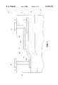
- FIG. 1illustrates a cross sectional view of one embodiment of the integrated circuit capacitor according to the present invention
- FIG. 2illustrates a top view of different masks used to produce the integrated circuit capacitor according to the present invention illustrated in FIG. 1;
- FIGS. 3A-3Fillustrates various steps in the process of forming the integrated circuit capacitor according to the present invention illustrated in FIG. 1;
- FIG. 4illustrates a cross sectional view of another embodiment of the integrated circuit capacitor according to the present invention.
- FIG. 5illustrates a cross sectional view of the integrated circuit capacitor according to the present invention connected to another circuit device disposed within the integrated circuit chip;
- FIG. 6illustrates a cross sectional view of another embodiment of the integrated circuit capacitor according to the present invention.
- FIGS. 7A and 7Billustrate cross sectional views of different embodiments of a floating gate circuit device according to the present invention
- FIG. 8illustrates a cross sectional view of an abrupt junction polysilicon diode integrated circuit device according to the present invention
- FIG. 9illustrates a cross sectional view of integrated circuit capacitors according to the present invention formed on different levels and connected to other circuit devices that form part of the integrated circuit chip;
- FIGS. 10A and 10Billustrate a cross sectional view and schematic, respectively, of integrated circuit capacitors according to the present invention formed on different levels and connected in series;
- FIGS. 11A and 11Billustrate a cross sectional view and schematic, respectively, of integrated circuit capacitors according to the present invention formed on different levels and connected in parallel.
- FIG. 1illustrates a cross sectional view of one embodiment of the integrated circuit capacitor according to the present invention.
- the portion of integrated circuit 10 that is illustratedshows the integrated circuit capacitor 12 according to the present invention being embedded on a dielectric 14 that is deposited over a substrate or underlying film 16.
- a dielectric 14that is deposited over a substrate or underlying film 16.
- a bottom electrode 18 made from an appropriate conductor such as polysilicon, metal or superconductive materialis disposed over a portion of the dielectric 14.
- bottom electrode 18will typically be about 4 ⁇ m ⁇ 1 ⁇ m to 1,000 ⁇ m ⁇ 1,000 ⁇ m and have a thickness of about 2,000 to 7,000 Angstroms.
- a capacitor dielectric 20is positioned over a portion of the bottom electrode 18.
- Capacitor dielectric 20is preferably a high dielectric constant insulator such as tantalum pentoxide (TaO 5 ), however silicon nitride, plasma oxides and other insulators, including composite dielectric, dielectrics with a graded dielectric constant, or ferroelectric dielectric materials could be used as well.
- a portion 18A of the bottom electrode 18is not covered by the capacitor dielectric 20 so that electrical contact with contact vias can be established, as will be discussed hereafter.
- the capacitor dielectric 20contains a central region 20A that is substantially planar and will typically be 4 ⁇ m ⁇ 1 ⁇ m to 1,000 ⁇ m ⁇ 1,000 ⁇ m and about 300 to 1,000 Angstroms thick, although the thickness will vary according to the desired capacitive characteristics of the capacitor 12. Also included is a peripheral portion 20B that has a predetermined height above the central region 20A. This height is typically about 2,000 to 7,000 Angstroms and its width is dependent on the thickness of central region 20A. Disposed above the central region 20A and within said peripheral region 20B is a top electrode 24 made from an appropriate conductor such as polysilicon, metal or superconductive material and which will typically have a thickness of about 2,000 to 7,000 Angstroms.
- an insulator 26Disposed on the sides and on top of the capacitor 12 is an insulator 26, which is preferably a material having a low dielectric constant, such as LTOPSG, BPSG, TEOS, or a spin on glass (SOG) material.
- Contact vias 28 and 30electrically connect the bottom electrode 18 and top electrode 24, respectively, to a patterned wiring layer 32, preferably a metal such as aluminum or tungsten, disposed above the capacitor 12.
- FIG. 2illustrates the mask levels used to produce the capacitor 12 illustrated in FIG. 1.
- Four different masks 50, 52, 54 and 56are required to make this structure, assuming that the levels below the bottom electrode 18 of FIG. 1 have already been made. It should be noted that only one mask in addition to those typically used for structures that do not include capacitors is required.
- Mask 50 illustrated in FIG. 2is used to obtain the bottom electrode 18 as shown in FIG. 3A, bottom electrode 18 is formed on insulator 14.
- Mask 50will not typically be an additional mask, since such a mask is typically used to obtain other lower level conductors.
- bottom electrodecan also be formed to provide for the formation of electrode 18 and other similar electrodes if desired.
- FIG. 3Billustrates the formation of insulation layer 70, which will become a portion of insulator 26 illustrated in FIG. 1. This layer is deposited over the whole surface and no masking is required.
- FIG. 3Cillustrates the formation of an opening 72 that is made in the insulation layer 70 such that a portion of the top surface of bottom electrode 18 is exposed. Opening 72 is made using an ion beam etch, an isotropic (wet) chemical or an anisotropic plasma reactive ion etch, depending on step coverage constraints and other design variables, and requires the use of mask 52 illustrated in FIG. 2 to define the dimensions of opening 72.
- ion beam etchan isotropic (wet) chemical or an anisotropic plasma reactive ion etch
- FIG. 3Dillustrates formation of intermediate film 74 (which will subsequently be etched to form the capacitor dielectric 20 illustrated in FIG. 1) and a conductive layer 76 (which will subsequently be polished to form the top electrode 24 illustrated in FIG. 1) over the exposed surfaces, including sidewall 72A of opening 72, illustrated in FIG. 3C, These materials are deposited after the mask 52 is removed and no additional mask is required for this deposition.
- FIG. 3Eillustrates the use of chemical mechanical polishing to polish the structure obtained in FIG. 3D until the entire surface is planar and coincides with the top planar surface 24A of the top electrode 24 that results from the etching of conductive layer 76.
- One of two or more CMP passescan be made to obtain desired polishing of the dielectric and electrode materials.
- the use of chemical mechanical polishingreduces exposure of the capacitor dielectric 20 to moisture, which allows ferroelectric dielectric materials to be used, as previously noted.
- other etch-back processescan be used, although a chemical mechanical polishing is presently preferred.
- FIG. 3Fillustrates the formation of an insulation layer 78, which forms another portion of insulator 26 illustrated in FIG. 1, Insulation layer 78 will typically be the same material as insulation layer 70 illustrated in FIG. 3B and be a relatively thick dielectric. Thereafter, mask 54 illustrated in FIG. 2 is applied and a chemical or reactive ion etch is used depending on the material to establish passages 80 and 82 illustrated in FIG. 3F that will eventually be filled with a conductive material to establish contact vias 28 and 30 illustrated in FIG. 1.
- the conductive material used to establish contact vias 28 and 30can be the same as the metal layer used to establish patterned wiring layer 32 illustrated in FIG. 1. Alternatively, chemical-mechanical polishing using tungsten plugs can be used to establish passages 80 and 82, as illustrated in FIG.
- passages 80 and 82are filled with a tungsten and a glue layer of Ti, TiN or both and, subsequently, chemical mechanical polishing is used to establish a planar surface containing tungsten plug contact vias, over which a metal patterned wiring layer can then be formed, as described hereinafter.
- a metal layer(not shown) is subsequently applied over the entire surface, and mask 56 illustrated in FIG. 2 is applied over this metal layer.
- the metal layeris then etched so that patterned wiring layer 32 illustrated in FIG. 1 results, which patterned wiring includes contact terminals connected to the bottom electrode 18 by the contact via 28 and the top electrode 24 by the contact via 30.
- FIG. 4illustrates a modification of the embodiment illustrated in FIG. 1 in which the insulator layer 78 illustrated in FIG. 3F is not applied. As a result, only a single contact via 28 is required.
- FIGS. 5illustrates the integrated circuit capacitor according to the present invention connected to another circuit device disposed within the semiconductor chip.
- FIG. 5illustrates capacitor 90 connected to a MOS transistor 92.
- Capacitor 90contains a bottom electrode 92 made of polysilicon, which is made at the same time and using the same mask as is used to make the polysilicon gate electrode 98 of MOS transistor 92.
- Top electrode 94is also made of a polysilicon or metal material and fabricated as described previously. As illustrated, top electrode 94 connects to the source/drain of transistor 96 by the electrical path that includes contact via 100, patterned wiring 102 and contact via 104, each of which are preferably made according to the process described previously. A contact via to layer 92 has not been illustrated.
- FIG. 6illustrates a further modification of the integrated circuit capacitor previously described with reference to FIG. 1.
- capacitor 110includes a bottom electrode 18 that contains a sidewall portion 18B that is disposed along the outer periphery of the dielectric 20.
- the same materialis preferably used to make the whole bottom electrode 18, although an additional process step, not needed to manufacture the capacitor illustrated in FIG. 1, is required.
- the first material depositedwill be a conductive layer made of the same material as the previously deposited material used to make the lower portion of bottom electrode 18. Thereafter, the remaining process steps are the same.
- This modificationresults in the structure illustrated in FIG. 6, which has an increased effective capacitor area due to the presence of sidewall 18B of the bottom electrode 18.
- FIG. 7Aillustrates another semiconductor device that can be fabricated according to the present invention.
- the floating gate device 120contains a bottom electrode 122, a tunnelling oxide 124, a floating electrode 126, another tunnelling oxide 128 and a top electrode 130. Additional and different process steps than those described with reference to the capacitor 12 of FIG. 1 previously described include the use of a tunnelling oxide, preferably an oxide, SiN 4 , or an oxide sandwich, rather than the dielectric material used as the dielectric 20 of the capacitor 12 of FIG. 1. Further, after formation of opening 72 as previously described with reference to FIG.
- layers which will correspond to each of tunnelling oxide 124, floating electrode 126, tunnelling oxide 128 and top electrode 130are sequentially deposited prior to the use of an etch that is preferably the chemical-mechanical polishing described previously with reference to FIG. 3E.
- the thickness of each of the above described layerswill vary according to the described electrical characteristics, but are typically about 80 Angstroms for the tunneling oxides and 2,000 to 7,000 Angstroms for the electrodes.
- a silicon nitride layercan be used as the floating electrode 126. With the process modified as indicated above, the floating gate device 120 of FIG. 7 will result.
- FIG. 7Billustrates another embodiment of another floating gate device 120A that is similar to that of floating gate device 120 illustrated in FIG. 7A, but differently contains a top electrode 130A that has a reduced size as compared to top electrode 130 in the FIG. 7A embodiment.
- fabrication of top electrode 130Arequires the use of an additional mask, it allows for further control of the tunneling characteristics due the change in the area ratios of between the capacitor formed with dielectric layer 128 and the capacitor formed with dielectric layer 124, since, if the thickness of dielectric layers 124 and 128 are equal, the highest field will appear on the smallest area of the tunnel capacitor.
- FIG. 8illustrates another semiconductor device that can be fabricated according to the present invention.
- the polysilicon diode device 140contains a bottom electrode 142, a dielectric layer 144 and a diode 146 formed from a n+ material region 148 and a p+ material region 150.
- Manufacture of this deviceis essentially the same as that described with reference to the capacitor 12 of FIG. 1, except for an additional step(s) of doping portions of what is designated the top electrode 24 illustrated in FIG. 1 to obtain the diode 146.
- Doping of n+ material region 148 and p+ material region 150will require at one additional mask step with a mask that covers one of n+ material region 148 and p+ material region 150 so that the other region can be formed.
- contact vias 152 and 154, each connected with one of n+ material region 148 and a p+ material region 150are required, rather than the single contact via 30 that is used with the capacitor 12 illustrated in FIG. 1.
- FIG. 9illustrates integrated circuit capacitors according to the present invention formed on different levels and connected to other circuit devices that form part of the integrated circuit chip.
- a CMOS inverter 160 containing an NMOS transistor 162 and a PMOS transistor 164is connected to multi-level integrated circuit capacitors of the present invention.
- Contact vias 166, 168, 170 and 172are formed in insulator 163 prior to the formation of a patterned wiring layer 174 that will include the bottom electrode 174A of a capacitor 176 formed according to the present invention as previously described so that a dielectric 178 and a top electrode 180 are also obtained.
- another capacitor 182is formed having a bottom electrode 184A which is part of a patterned wiring layer 184, a dielectric 186 and a top electrode 188.
- a passage for formation of contact via 189is established prior to formation of patterned wiring layer 180 so that top electrode 180 of capacitor 176 connects to the bottom electrode 184A of capacitor 182.
- contact viassuch as contact via 190 and wiring paths such as conductive paths 174B and 184B are also formed so that desired connections of different devices can be obtained. Steps subsequent to the formation of the multi-level capacitors use the same process steps previously described and such will not be repeated.
- FIG. 9also illustrates that the bottom electrode 174A and conductive path 174B are formed after global planarization of the insulator 163. This produces a flat bottom surface on which many bottom electrodes can be formed, if desired. Thus, the area of the bottom electrodes can be well controlled and not dependent on the underlying topology. This allows for accurate matching of capacitors.
- FIGS. 10A and 10B, and FIGS. 11A and 11Brespectively illustrate series and parallel connections of capacitors that are formed according to the present invention.
- FIGS. 10A and 10Billustrate capacitors 200, 202 and 204, which are connected in series using contact vias 206 and 208, with terminals 210 and 212, each having an associated contact via 210A and 212A, being formed so that a voltage divider is obtained.
- each of the capacitors 200, 202 and 204are formed on a different level of the semiconductor chip. It should be noted that each of these capacitors are offset from the capacitor below so that appropriate connections using contact vias and patterned wiring can be established, although this specific offset scheme is not required if one considers wiring that is orthogonal to the plane of the paper of the drawing figures.
- FIGS. 11A and 11Billustrate capacitors 220, 222 and 224, which are connected in parallel using contact vias 226 and 228, with terminal 230, formed from contact vias 230 A-E and patterned wiring conductors 230 F-H. It is again noted that each of these capacitors are offset from the capacitor below so that appropriate connections using contact vias and patterned wiring can be established, although this specific offset scheme is not required if one considers wiring that is orthogonal to the plane of the paper of the drawing figures. Further, while the electrical connection between different levels can use a single single contact via 210A, as illustrated in FIG. 10A, stacked vias, as illustrated by vias 230A, 230B and 230D in FIG. 11A can also be used.
Landscapes
- Semiconductor Integrated Circuits (AREA)
- Metal-Oxide And Bipolar Metal-Oxide Semiconductor Integrated Circuits (AREA)
- Semiconductor Memories (AREA)
- Internal Circuitry In Semiconductor Integrated Circuit Devices (AREA)
Abstract
Description
Claims (25)
Priority Applications (6)
| Application Number | Priority Date | Filing Date | Title |
|---|---|---|---|
| US08/673,655US6115233A (en) | 1996-06-28 | 1996-06-28 | Integrated circuit device having a capacitor with the dielectric peripheral region being greater than the dielectric central region |
| EP97928352AEP0907968A1 (en) | 1996-06-28 | 1997-06-25 | Integrated circuit device and method of making the same |
| AU32677/97AAU3267797A (en) | 1996-06-28 | 1997-06-25 | Integrated circuit device and method of making the same |
| JP50390698AJP2002508113A (en) | 1996-06-28 | 1997-06-25 | Integrated circuit device and manufacturing method thereof |
| PCT/GB1997/001699WO1998000872A1 (en) | 1996-06-28 | 1997-06-25 | Integrated circuit device and method of making the same |
| US09/431,439US6284586B1 (en) | 1996-06-28 | 1999-11-01 | Integrated circuit device and method of making the same using chemical mechanical polishing to remove material in two layers following masking |
Applications Claiming Priority (1)
| Application Number | Priority Date | Filing Date | Title |
|---|---|---|---|
| US08/673,655US6115233A (en) | 1996-06-28 | 1996-06-28 | Integrated circuit device having a capacitor with the dielectric peripheral region being greater than the dielectric central region |
Related Child Applications (1)
| Application Number | Title | Priority Date | Filing Date |
|---|---|---|---|
| US09/431,439DivisionUS6284586B1 (en) | 1996-06-28 | 1999-11-01 | Integrated circuit device and method of making the same using chemical mechanical polishing to remove material in two layers following masking |
Publications (1)
| Publication Number | Publication Date |
|---|---|
| US6115233Atrue US6115233A (en) | 2000-09-05 |
Family
ID=24703561
Family Applications (2)
| Application Number | Title | Priority Date | Filing Date |
|---|---|---|---|
| US08/673,655Expired - LifetimeUS6115233A (en) | 1996-06-28 | 1996-06-28 | Integrated circuit device having a capacitor with the dielectric peripheral region being greater than the dielectric central region |
| US09/431,439Expired - LifetimeUS6284586B1 (en) | 1996-06-28 | 1999-11-01 | Integrated circuit device and method of making the same using chemical mechanical polishing to remove material in two layers following masking |
Family Applications After (1)
| Application Number | Title | Priority Date | Filing Date |
|---|---|---|---|
| US09/431,439Expired - LifetimeUS6284586B1 (en) | 1996-06-28 | 1999-11-01 | Integrated circuit device and method of making the same using chemical mechanical polishing to remove material in two layers following masking |
Country Status (5)
| Country | Link |
|---|---|
| US (2) | US6115233A (en) |
| EP (1) | EP0907968A1 (en) |
| JP (1) | JP2002508113A (en) |
| AU (1) | AU3267797A (en) |
| WO (1) | WO1998000872A1 (en) |
Cited By (39)
| Publication number | Priority date | Publication date | Assignee | Title |
|---|---|---|---|---|
| US20020025759A1 (en)* | 2000-08-30 | 2002-02-28 | Whonchee Lee | Microelectronic substrate having conductive material with blunt cornered apertures, and associated methods for removing conductive material |
| US6372524B1 (en) | 2001-03-06 | 2002-04-16 | Lsi Logic Corporation | Method for CMP endpoint detection |
| US6503828B1 (en) | 2001-06-14 | 2003-01-07 | Lsi Logic Corporation | Process for selective polishing of metal-filled trenches of integrated circuit structures |
| EP1283545A2 (en) | 2001-08-10 | 2003-02-12 | Rohm Co., Ltd. | Semiconductor device having ferroelectric substance capacitor |
| US20030054729A1 (en)* | 2000-08-30 | 2003-03-20 | Whonchee Lee | Methods and apparatus for electromechanically and/or electrochemically-mechanically removing conductive material from a microelectronic substrate |
| US6541383B1 (en) | 2000-06-29 | 2003-04-01 | Lsi Logic Corporation | Apparatus and method for planarizing the surface of a semiconductor wafer |
| US20030129927A1 (en)* | 2000-08-30 | 2003-07-10 | Whonchee Lee | Methods and apparatus for selectively removing conductive material from a microelectronic substrate |
| US6606793B1 (en)* | 2000-07-31 | 2003-08-19 | Motorola, Inc. | Printed circuit board comprising embedded capacitor and method of same |
| US20030178696A1 (en)* | 2002-03-25 | 2003-09-25 | Eric Adler | One-mask metal-insulator-metal capacitor and method for forming same |
| US20030226764A1 (en)* | 2000-08-30 | 2003-12-11 | Moore Scott E. | Methods and apparatus for electrochemical-mechanical processing of microelectronic workpieces |
| US20040043629A1 (en)* | 2002-08-29 | 2004-03-04 | Whonchee Lee | Method and apparatus for removing adjacent conductive and nonconductive materials of a microelectronic substrate |
| US20040043582A1 (en)* | 2002-08-29 | 2004-03-04 | Dinesh Chopra | Method and apparatus for simultaneously removing multiple conductive materials from microelectronic substrates |
| US6787911B1 (en)* | 1998-09-22 | 2004-09-07 | Newport Fab, Llc | Interconnect with low dielectric constant insulators for semiconductor integrated circuit manufacturing |
| US20050035000A1 (en)* | 2000-08-30 | 2005-02-17 | Whonchee Lee | Methods and apparatus for electrically and/or chemically-mechanically removing conductive material from a microelectronic substrate |
| US6867448B1 (en)* | 2000-08-31 | 2005-03-15 | Micron Technology, Inc. | Electro-mechanically polished structure |
| US20050059324A1 (en)* | 2003-09-17 | 2005-03-17 | Whonchee Lee | Methods and apparatus for removing conductive material from a microelectronic substrate |
| US20050196963A1 (en)* | 2004-02-20 | 2005-09-08 | Whonchee Lee | Methods and apparatuses for electrochemical-mechanical polishing |
| US6964924B1 (en) | 2001-09-11 | 2005-11-15 | Lsi Logic Corporation | Integrated circuit process monitoring and metrology system |
| US20060081960A1 (en)* | 2004-10-20 | 2006-04-20 | Advanced Semiconductor Engineering Inc. | Integrated capacitor on packaging substrate |
| US20060148108A1 (en)* | 2005-01-06 | 2006-07-06 | Fujitsu Limited | Method for fabricating semiconductor device |
| US7074113B1 (en) | 2000-08-30 | 2006-07-11 | Micron Technology, Inc. | Methods and apparatus for removing conductive material from a microelectronic substrate |
| US7112121B2 (en) | 2000-08-30 | 2006-09-26 | Micron Technology, Inc. | Methods and apparatus for electrical, mechanical and/or chemical removal of conductive material from a microelectronic substrate |
| US7134934B2 (en) | 2000-08-30 | 2006-11-14 | Micron Technology, Inc. | Methods and apparatus for electrically detecting characteristics of a microelectronic substrate and/or polishing medium |
| US7192335B2 (en) | 2002-08-29 | 2007-03-20 | Micron Technology, Inc. | Method and apparatus for chemically, mechanically, and/or electrolytically removing material from microelectronic substrates |
| US20070209201A1 (en)* | 2003-11-28 | 2007-09-13 | Koutsaroff Ivoyl P | Multi-level thin film capacitor on a ceramic substrate and method of manufacturing the same |
| US20080116505A1 (en)* | 2006-11-20 | 2008-05-22 | Shih Wei Wang | Non-volatile memory cells formed in back-end-of line processes |
| US7566391B2 (en) | 2004-09-01 | 2009-07-28 | Micron Technology, Inc. | Methods and systems for removing materials from microfeature workpieces with organic and/or non-aqueous electrolytic media |
| US20110070718A1 (en)* | 2006-06-08 | 2011-03-24 | Kim Yoon-Hae | Semiconductor device and method of fabricating the same |
| US20110210806A1 (en)* | 2007-07-16 | 2011-09-01 | Us Government As Represented By The Secretary Of The Army | Thin film compositionally stratified multi-layer heterostructure for temperature insensitive low dielectric loss and enhanced tunablity otm communications devices and methods for fabrication thereof |
| US9219110B2 (en) | 2014-04-10 | 2015-12-22 | Taiwan Semiconductor Manufacturing Co., Ltd. | MIM capacitor structure |
| US9368392B2 (en) | 2014-04-10 | 2016-06-14 | Taiwan Semiconductor Manufacturing Co., Ltd. | MIM capacitor structure |
| US9391016B2 (en)* | 2014-04-10 | 2016-07-12 | Taiwan Semiconductor Manufacturing Co., Ltd. | MIM capacitor structure |
| US9425061B2 (en) | 2014-05-29 | 2016-08-23 | Taiwan Semiconductor Manufacturing Co., Ltd. | Buffer cap layer to improve MIM structure performance |
| US9506153B2 (en) | 2014-09-17 | 2016-11-29 | The United States Of America As Represented By The Secretary Of The Army | Integrated composite perovskite oxide heterostructure |
| US9681509B2 (en)* | 2015-03-06 | 2017-06-13 | Samsung Electronics Co., Ltd. | Light-emitting device package and electronic device including light-emitting device |
| US9831171B2 (en)* | 2014-11-12 | 2017-11-28 | Infineon Technologies Ag | Capacitors with barrier dielectric layers, and methods of formation thereof |
| US10032853B2 (en) | 2014-09-17 | 2018-07-24 | The United States Of America As Represented By The Secretary Of The Army | Microstructural architecture to enable strain relieved non-linear complex oxide thin films |
| CN111295766A (en)* | 2017-12-29 | 2020-06-16 | 德州仪器公司 | High voltage isolation structure and method |
| CN115360018A (en)* | 2022-07-25 | 2022-11-18 | 中国科学院物理研究所 | Ferroelectric capacitor and method for manufacturing the same |
Families Citing this family (18)
| Publication number | Priority date | Publication date | Assignee | Title |
|---|---|---|---|---|
| US6511877B2 (en) | 1997-07-17 | 2003-01-28 | Kabushiki Kaisha Toshiba | Semiconductor integrated circuit and method for manufacturing the same |
| FR2781603B1 (en)* | 1998-07-21 | 2000-10-06 | St Microelectronics Sa | METHOD FOR FORMING CAPACITY ON AN INTEGRATED CIRCUIT |
| US6432791B1 (en)* | 1999-04-14 | 2002-08-13 | Texas Instruments Incorporated | Integrated circuit capacitor and method |
| WO2001018830A1 (en)* | 1999-09-06 | 2001-03-15 | Forschungszentrum Jülich GmbH | Thin-film capacitor |
| US6603161B2 (en)* | 2000-03-10 | 2003-08-05 | Kabushiki Kaisha Toshiba | Semiconductor device having ferroelectric capacitor and method for manufacturing the same |
| US6426249B1 (en)* | 2000-03-16 | 2002-07-30 | International Business Machines Corporation | Buried metal dual damascene plate capacitor |
| DE10022655C2 (en)* | 2000-04-28 | 2002-03-07 | Infineon Technologies Ag | Process for the production of capacitor structures |
| US6440845B1 (en)* | 2000-10-05 | 2002-08-27 | United Microelectronics Corp. | Method of fabricating interconnect of capacitor |
| JP2004523924A (en)* | 2001-03-21 | 2004-08-05 | コーニンクレッカ フィリップス エレクトロニクス エヌ ヴィ | Electronic device |
| US6677635B2 (en)* | 2001-06-01 | 2004-01-13 | Infineon Technologies Ag | Stacked MIMCap between Cu dual damascene levels |
| US20030082671A1 (en) | 2001-07-24 | 2003-05-01 | Thomas Hoeg-Jensen | Method for making acylated polypeptides |
| ITRM20010517A1 (en)* | 2001-08-29 | 2003-02-28 | Micron Technology Inc | STRUCTURE OF INTEGRATED POLYSILIC CAPACITOR. |
| JP2004015059A (en)* | 2002-06-05 | 2004-01-15 | Texas Instruments Inc | Precision analog capacitor with low voltage coefficient and hysteresis and innovative method of construction |
| KR101198346B1 (en) | 2003-04-08 | 2012-11-06 | 노보 노르디스크 에이/에스 | Regeneration of chromatographic stationary phases |
| FR2886050A1 (en)* | 2005-05-18 | 2006-11-24 | St Microelectronics Crolles 2 | INTEGRATED CAPACITOR WITH HIGH CLAMP VOLTAGE |
| US7915129B2 (en)* | 2009-04-22 | 2011-03-29 | Polar Semiconductor, Inc. | Method of fabricating high-voltage metal oxide semiconductor transistor devices |
| KR101596460B1 (en)* | 2011-10-01 | 2016-02-26 | 인텔 코포레이션 | On-chip capacitors and methods of assembling same |
| DE112022001264T5 (en)* | 2021-03-29 | 2023-12-14 | Rohm Co., Ltd. | ISOLATOR, ISOLATOR MODULE AND GATE DRIVER |
Citations (78)
| Publication number | Priority date | Publication date | Assignee | Title |
|---|---|---|---|---|
| US4793895A (en)* | 1988-01-25 | 1988-12-27 | Ibm Corporation | In situ conductivity monitoring technique for chemical/mechanical planarization endpoint detection |
| US4849854A (en)* | 1986-11-12 | 1989-07-18 | Mitsubihsi Denki Kabushiki Kaisha | Semiconductor device and method of manufacturing the same |
| EP0374971A2 (en)* | 1988-12-23 | 1990-06-27 | Matsushita Electric Industrial Co., Ltd. | Three-dimensionally stacked LSI |
| US5036015A (en)* | 1990-09-24 | 1991-07-30 | Micron Technology, Inc. | Method of endpoint detection during chemical/mechanical planarization of semiconductor wafers |
| US5057447A (en)* | 1990-07-09 | 1991-10-15 | Texas Instruments Incorporated | Silicide/metal floating gate process |
| US5081421A (en)* | 1990-05-01 | 1992-01-14 | At&T Bell Laboratories | In situ monitoring technique and apparatus for chemical/mechanical planarization endpoint detection |
| US5151584A (en)* | 1988-07-20 | 1992-09-29 | Applied Materials, Inc. | Method and apparatus for endpoint detection in a semiconductor wafer etching system |
| US5160987A (en)* | 1989-10-26 | 1992-11-03 | International Business Machines Corporation | Three-dimensional semiconductor structures formed from planar layers |
| US5169491A (en)* | 1991-07-29 | 1992-12-08 | Micron Technology, Inc. | Method of etching SiO2 dielectric layers using chemical mechanical polishing techniques |
| US5196353A (en)* | 1992-01-03 | 1993-03-23 | Micron Technology, Inc. | Method for controlling a semiconductor (CMP) process by measuring a surface temperature and developing a thermal image of the wafer |
| US5222329A (en)* | 1992-03-26 | 1993-06-29 | Micron Technology, Inc. | Acoustical method and system for detecting and controlling chemical-mechanical polishing (CMP) depths into layers of conductors, semiconductors, and dielectric materials |
| US5240552A (en)* | 1991-12-11 | 1993-08-31 | Micron Technology, Inc. | Chemical mechanical planarization (CMP) of a semiconductor wafer using acoustical waves for in-situ end point detection |
| EP0557937A1 (en)* | 1992-02-25 | 1993-09-01 | Ramtron International Corporation | Ozone gas processing for ferroelectric memory circuits |
| US5245794A (en)* | 1992-04-09 | 1993-09-21 | Advanced Micro Devices, Inc. | Audio end point detector for chemical-mechanical polishing and method therefor |
| US5245790A (en)* | 1992-02-14 | 1993-09-21 | Lsi Logic Corporation | Ultrasonic energy enhanced chemi-mechanical polishing of silicon wafers |
| US5246884A (en)* | 1991-10-30 | 1993-09-21 | International Business Machines Corporation | Cvd diamond or diamond-like carbon for chemical-mechanical polish etch stop |
| US5265378A (en)* | 1992-07-10 | 1993-11-30 | Lsi Logic Corporation | Detecting the endpoint of chem-mech polishing and resulting semiconductor device |
| US5272115A (en)* | 1991-01-09 | 1993-12-21 | Nec Corporation | Method of leveling the laminated surface of a semiconductor substrate |
| US5302233A (en)* | 1993-03-19 | 1994-04-12 | Micron Semiconductor, Inc. | Method for shaping features of a semiconductor structure using chemical mechanical planarization (CMP) |
| US5306935A (en)* | 1988-12-21 | 1994-04-26 | Texas Instruments Incorporated | Method of forming a nonvolatile stacked memory |
| US5308438A (en)* | 1992-01-30 | 1994-05-03 | International Business Machines Corporation | Endpoint detection apparatus and method for chemical/mechanical polishing |
| US5310455A (en)* | 1992-07-10 | 1994-05-10 | Lsi Logic Corporation | Techniques for assembling polishing pads for chemi-mechanical polishing of silicon wafers |
| US5330931A (en)* | 1993-09-22 | 1994-07-19 | Northern Telecom Limited | Method of making a capacitor for an integrated circuit |
| US5337015A (en)* | 1993-06-14 | 1994-08-09 | International Business Machines Corporation | In-situ endpoint detection method and apparatus for chemical-mechanical polishing using low amplitude input voltage |
| US5354712A (en)* | 1992-11-12 | 1994-10-11 | Northern Telecom Limited | Method for forming interconnect structures for integrated circuits |
| US5356826A (en)* | 1992-08-07 | 1994-10-18 | Yamaha Corporation | Method of manufacturing semiconductor device provided with capacitor and resistor |
| US5362669A (en)* | 1993-06-24 | 1994-11-08 | Northern Telecom Limited | Method of making integrated circuits |
| US5389194A (en)* | 1993-02-05 | 1995-02-14 | Lsi Logic Corporation | Methods of cleaning semiconductor substrates after polishing |
| US5395801A (en)* | 1993-09-29 | 1995-03-07 | Micron Semiconductor, Inc. | Chemical-mechanical polishing processes of planarizing insulating layers |
| US5399234A (en)* | 1993-09-29 | 1995-03-21 | Motorola Inc. | Acoustically regulated polishing process |
| US5403228A (en)* | 1992-07-10 | 1995-04-04 | Lsi Logic Corporation | Techniques for assembling polishing pads for silicon wafer polishing |
| US5405806A (en)* | 1994-03-29 | 1995-04-11 | Motorola Inc. | Method for forming a metal silicide interconnect in an integrated circuit |
| US5422289A (en)* | 1992-04-27 | 1995-06-06 | National Semiconductor Corporation | Method of manufacturing a fully planarized MOSFET and resulting structure |
| US5439551A (en)* | 1994-03-02 | 1995-08-08 | Micron Technology, Inc. | Chemical-mechanical polishing techniques and methods of end point detection in chemical-mechanical polishing processes |
| US5479316A (en)* | 1993-08-24 | 1995-12-26 | Analog Devices, Inc. | Integrated circuit metal-oxide-metal capacitor and method of making same |
| US5483568A (en)* | 1994-11-03 | 1996-01-09 | Kabushiki Kaisha Toshiba | Pad condition and polishing rate monitor using fluorescence |
| US5492594A (en)* | 1994-09-26 | 1996-02-20 | International Business Machines Corp. | Chemical-mechanical polishing tool with end point measurement station |
| US5531861A (en)* | 1993-09-29 | 1996-07-02 | Motorola, Inc. | Chemical-mechanical-polishing pad cleaning process for use during the fabrication of semiconductor devices |
| US5559428A (en)* | 1995-04-10 | 1996-09-24 | International Business Machines Corporation | In-situ monitoring of the change in thickness of films |
| US5561541A (en)* | 1984-09-05 | 1996-10-01 | The United States Of America As Represented By The Secretary Of The Army | Frustrated total internal reflection optical power limiter |
| US5595526A (en)* | 1994-11-30 | 1997-01-21 | Intel Corporation | Method and apparatus for endpoint detection in a chemical/mechanical process for polishing a substrate |
| US5597442A (en)* | 1995-10-16 | 1997-01-28 | Taiwan Semiconductor Manufacturing Company Ltd. | Chemical/mechanical planarization (CMP) endpoint method using measurement of polishing pad temperature |
| US5626715A (en)* | 1993-02-05 | 1997-05-06 | Lsi Logic Corporation | Methods of polishing semiconductor substrates |
| US5637185A (en)* | 1995-03-30 | 1997-06-10 | Rensselaer Polytechnic Institute | Systems for performing chemical mechanical planarization and process for conducting same |
| US5639388A (en)* | 1995-01-19 | 1997-06-17 | Ebara Corporation | Polishing endpoint detection method |
| US5644221A (en)* | 1996-03-19 | 1997-07-01 | International Business Machines Corporation | Endpoint detection for chemical mechanical polishing using frequency or amplitude mode |
| US5643046A (en)* | 1994-02-21 | 1997-07-01 | Kabushiki Kaisha Toshiba | Polishing method and apparatus for detecting a polishing end point of a semiconductor wafer |
| US5643050A (en)* | 1996-05-23 | 1997-07-01 | Industrial Technology Research Institute | Chemical/mechanical polish (CMP) thickness monitor |
| US5647952A (en)* | 1996-04-01 | 1997-07-15 | Industrial Technology Research Institute | Chemical/mechanical polish (CMP) endpoint method |
| US5658183A (en)* | 1993-08-25 | 1997-08-19 | Micron Technology, Inc. | System for real-time control of semiconductor wafer polishing including optical monitoring |
| US5660672A (en)* | 1995-04-10 | 1997-08-26 | International Business Machines Corporation | In-situ monitoring of conductive films on semiconductor wafers |
| US5663797A (en)* | 1996-05-16 | 1997-09-02 | Micron Technology, Inc. | Method and apparatus for detecting the endpoint in chemical-mechanical polishing of semiconductor wafers |
| US5664987A (en)* | 1994-01-31 | 1997-09-09 | National Semiconductor Corporation | Methods and apparatus for control of polishing pad conditioning for wafer planarization |
| US5667629A (en)* | 1996-06-21 | 1997-09-16 | Chartered Semiconductor Manufactuing Pte, Ltd. | Method and apparatus for determination of the end point in chemical mechanical polishing |
| US5667433A (en)* | 1995-06-07 | 1997-09-16 | Lsi Logic Corporation | Keyed end effector for CMP pad conditioner |
| US5667424A (en)* | 1996-09-25 | 1997-09-16 | Chartered Semiconductor Manufacturing Pte Ltd. | New chemical mechanical planarization (CMP) end point detection apparatus |
| US5668063A (en)* | 1995-05-23 | 1997-09-16 | Watkins Johnson Company | Method of planarizing a layer of material |
| US5670410A (en)* | 1996-09-25 | 1997-09-23 | Chartered Semiconductor Manufacturing Pte Ltd. | Method of forming integrated CMP stopper and analog capacitor |
| US5672091A (en)* | 1994-12-22 | 1997-09-30 | Ebara Corporation | Polishing apparatus having endpoint detection device |
| US5674784A (en)* | 1996-10-02 | 1997-10-07 | Taiwan Semiconductor Manufacturing Company, Ltd. | Method for forming polish stop layer for CMP process |
| US5695660A (en)* | 1992-09-17 | 1997-12-09 | Luxtron Corporation | Optical techniques of measuring endpoint during the processing of material layers in an optically hostile environment |
| US5700180A (en)* | 1993-08-25 | 1997-12-23 | Micron Technology, Inc. | System for real-time control of semiconductor wafer polishing |
| US5705435A (en)* | 1996-08-09 | 1998-01-06 | Industrial Technology Research Institute | Chemical-mechanical polishing (CMP) apparatus |
| US5708559A (en)* | 1995-10-27 | 1998-01-13 | International Business Machines Corporation | Precision analog metal-metal capacitor |
| US5710076A (en)* | 1996-09-03 | 1998-01-20 | Industrial Technology Research Institute | Method for fabricating a sub-half micron MOSFET device with global planarization of insulator filled shallow trenches, via the use of a bottom anti-reflective coating |
| US5712185A (en)* | 1996-04-23 | 1998-01-27 | United Microelectronics | Method for forming shallow trench isolation |
| US5722875A (en)* | 1995-05-30 | 1998-03-03 | Tokyo Electron Limited | Method and apparatus for polishing |
| US5741171A (en)* | 1996-08-19 | 1998-04-21 | Sagitta Engineering Solutions, Ltd. | Precision polishing system |
| US5777739A (en)* | 1996-02-16 | 1998-07-07 | Micron Technology, Inc. | Endpoint detector and method for measuring a change in wafer thickness in chemical-mechanical polishing of semiconductor wafers |
| US5861055A (en)* | 1995-12-29 | 1999-01-19 | Lsi Logic Corporation | Polishing composition for CMP operations |
| US5865666A (en)* | 1997-08-20 | 1999-02-02 | Lsi Logic Corporation | Apparatus and method for polish removing a precise amount of material from a wafer |
| US5868608A (en)* | 1996-08-13 | 1999-02-09 | Lsi Logic Corporation | Subsonic to supersonic and ultrasonic conditioning of a polishing pad in a chemical mechanical polishing apparatus |
| US5882251A (en)* | 1997-08-19 | 1999-03-16 | Lsi Logic Corporation | Chemical mechanical polishing pad slurry distribution grooves |
| US5888120A (en)* | 1997-09-29 | 1999-03-30 | Lsi Logic Corporation | Method and apparatus for chemical mechanical polishing |
| US5893756A (en)* | 1997-08-26 | 1999-04-13 | Lsi Logic Corporation | Use of ethylene glycol as a corrosion inhibitor during cleaning after metal chemical mechanical polishing |
| US5931719A (en)* | 1997-08-25 | 1999-08-03 | Lsi Logic Corporation | Method and apparatus for using pressure differentials through a polishing pad to improve performance in chemical mechanical polishing |
| US5948697A (en)* | 1996-05-23 | 1999-09-07 | Lsi Logic Corporation | Catalytic acceleration and electrical bias control of CMP processing |
| US5957757A (en)* | 1997-10-30 | 1999-09-28 | Lsi Logic Corporation | Conditioning CMP polishing pad using a high pressure fluid |
Family Cites Families (5)
| Publication number | Priority date | Publication date | Assignee | Title |
|---|---|---|---|---|
| KR100236531B1 (en)* | 1996-11-06 | 2000-01-15 | 윤종용 | Thin Film Capacitor Manufacturing Method |
| US6075266A (en)* | 1997-01-09 | 2000-06-13 | Kabushiki Kaisha Toshiba | Semiconductor device having MIS transistors and capacitor |
| CN1112731C (en)* | 1997-04-30 | 2003-06-25 | 三星电子株式会社 | Method for making capacitor used for analog function |
| JP3201468B2 (en)* | 1997-05-26 | 2001-08-20 | 日本電気株式会社 | Capacitive element and method of manufacturing the same |
| GB2337633B (en)* | 1998-05-20 | 2003-04-02 | Mitel Corp | Method of forming capacitors in a semiconductor device |
- 1996
- 1996-06-28USUS08/673,655patent/US6115233A/ennot_activeExpired - Lifetime
- 1997
- 1997-06-25JPJP50390698Apatent/JP2002508113A/enactivePending
- 1997-06-25WOPCT/GB1997/001699patent/WO1998000872A1/ennot_activeApplication Discontinuation
- 1997-06-25EPEP97928352Apatent/EP0907968A1/ennot_activeWithdrawn
- 1997-06-25AUAU32677/97Apatent/AU3267797A/ennot_activeAbandoned
- 1999
- 1999-11-01USUS09/431,439patent/US6284586B1/ennot_activeExpired - Lifetime
Patent Citations (82)
| Publication number | Priority date | Publication date | Assignee | Title |
|---|---|---|---|---|
| US5561541A (en)* | 1984-09-05 | 1996-10-01 | The United States Of America As Represented By The Secretary Of The Army | Frustrated total internal reflection optical power limiter |
| US4849854A (en)* | 1986-11-12 | 1989-07-18 | Mitsubihsi Denki Kabushiki Kaisha | Semiconductor device and method of manufacturing the same |
| US4793895A (en)* | 1988-01-25 | 1988-12-27 | Ibm Corporation | In situ conductivity monitoring technique for chemical/mechanical planarization endpoint detection |
| US5151584A (en)* | 1988-07-20 | 1992-09-29 | Applied Materials, Inc. | Method and apparatus for endpoint detection in a semiconductor wafer etching system |
| US5306935A (en)* | 1988-12-21 | 1994-04-26 | Texas Instruments Incorporated | Method of forming a nonvolatile stacked memory |
| EP0374971A2 (en)* | 1988-12-23 | 1990-06-27 | Matsushita Electric Industrial Co., Ltd. | Three-dimensionally stacked LSI |
| US5160987A (en)* | 1989-10-26 | 1992-11-03 | International Business Machines Corporation | Three-dimensional semiconductor structures formed from planar layers |
| US5081421A (en)* | 1990-05-01 | 1992-01-14 | At&T Bell Laboratories | In situ monitoring technique and apparatus for chemical/mechanical planarization endpoint detection |
| US5057447A (en)* | 1990-07-09 | 1991-10-15 | Texas Instruments Incorporated | Silicide/metal floating gate process |
| US5036015A (en)* | 1990-09-24 | 1991-07-30 | Micron Technology, Inc. | Method of endpoint detection during chemical/mechanical planarization of semiconductor wafers |
| US5272115A (en)* | 1991-01-09 | 1993-12-21 | Nec Corporation | Method of leveling the laminated surface of a semiconductor substrate |
| US5169491A (en)* | 1991-07-29 | 1992-12-08 | Micron Technology, Inc. | Method of etching SiO2 dielectric layers using chemical mechanical polishing techniques |
| US5246884A (en)* | 1991-10-30 | 1993-09-21 | International Business Machines Corporation | Cvd diamond or diamond-like carbon for chemical-mechanical polish etch stop |
| US5240552A (en)* | 1991-12-11 | 1993-08-31 | Micron Technology, Inc. | Chemical mechanical planarization (CMP) of a semiconductor wafer using acoustical waves for in-situ end point detection |
| US5196353A (en)* | 1992-01-03 | 1993-03-23 | Micron Technology, Inc. | Method for controlling a semiconductor (CMP) process by measuring a surface temperature and developing a thermal image of the wafer |
| US5308438A (en)* | 1992-01-30 | 1994-05-03 | International Business Machines Corporation | Endpoint detection apparatus and method for chemical/mechanical polishing |
| US5245790A (en)* | 1992-02-14 | 1993-09-21 | Lsi Logic Corporation | Ultrasonic energy enhanced chemi-mechanical polishing of silicon wafers |
| EP0557937A1 (en)* | 1992-02-25 | 1993-09-01 | Ramtron International Corporation | Ozone gas processing for ferroelectric memory circuits |
| US5222329A (en)* | 1992-03-26 | 1993-06-29 | Micron Technology, Inc. | Acoustical method and system for detecting and controlling chemical-mechanical polishing (CMP) depths into layers of conductors, semiconductors, and dielectric materials |
| US5245794A (en)* | 1992-04-09 | 1993-09-21 | Advanced Micro Devices, Inc. | Audio end point detector for chemical-mechanical polishing and method therefor |
| US5422289A (en)* | 1992-04-27 | 1995-06-06 | National Semiconductor Corporation | Method of manufacturing a fully planarized MOSFET and resulting structure |
| US5624304A (en)* | 1992-07-10 | 1997-04-29 | Lsi Logic, Inc. | Techniques for assembling polishing pads for chemi-mechanical polishing of silicon wafers |
| US5265378A (en)* | 1992-07-10 | 1993-11-30 | Lsi Logic Corporation | Detecting the endpoint of chem-mech polishing and resulting semiconductor device |
| US5310455A (en)* | 1992-07-10 | 1994-05-10 | Lsi Logic Corporation | Techniques for assembling polishing pads for chemi-mechanical polishing of silicon wafers |
| US5321304A (en)* | 1992-07-10 | 1994-06-14 | Lsi Logic Corporation | Detecting the endpoint of chem-mech polishing, and resulting semiconductor device |
| US5516400A (en)* | 1992-07-10 | 1996-05-14 | Lsi Logic Corporation | Techniques for assembling polishing pads for chemical-mechanical polishing of silicon wafers |
| US5403228A (en)* | 1992-07-10 | 1995-04-04 | Lsi Logic Corporation | Techniques for assembling polishing pads for silicon wafer polishing |
| US5356826A (en)* | 1992-08-07 | 1994-10-18 | Yamaha Corporation | Method of manufacturing semiconductor device provided with capacitor and resistor |
| US5695660A (en)* | 1992-09-17 | 1997-12-09 | Luxtron Corporation | Optical techniques of measuring endpoint during the processing of material layers in an optically hostile environment |
| US5354712A (en)* | 1992-11-12 | 1994-10-11 | Northern Telecom Limited | Method for forming interconnect structures for integrated circuits |
| US5389194A (en)* | 1993-02-05 | 1995-02-14 | Lsi Logic Corporation | Methods of cleaning semiconductor substrates after polishing |
| US5626715A (en)* | 1993-02-05 | 1997-05-06 | Lsi Logic Corporation | Methods of polishing semiconductor substrates |
| US5302233A (en)* | 1993-03-19 | 1994-04-12 | Micron Semiconductor, Inc. | Method for shaping features of a semiconductor structure using chemical mechanical planarization (CMP) |
| US5337015A (en)* | 1993-06-14 | 1994-08-09 | International Business Machines Corporation | In-situ endpoint detection method and apparatus for chemical-mechanical polishing using low amplitude input voltage |
| US5362669A (en)* | 1993-06-24 | 1994-11-08 | Northern Telecom Limited | Method of making integrated circuits |
| US5479316A (en)* | 1993-08-24 | 1995-12-26 | Analog Devices, Inc. | Integrated circuit metal-oxide-metal capacitor and method of making same |
| US5658183A (en)* | 1993-08-25 | 1997-08-19 | Micron Technology, Inc. | System for real-time control of semiconductor wafer polishing including optical monitoring |
| US5700180A (en)* | 1993-08-25 | 1997-12-23 | Micron Technology, Inc. | System for real-time control of semiconductor wafer polishing |
| US5452178A (en)* | 1993-09-22 | 1995-09-19 | Northern Telecom Limited | Structure and method of making a capacitor for an intergrated circuit |
| US5330931A (en)* | 1993-09-22 | 1994-07-19 | Northern Telecom Limited | Method of making a capacitor for an integrated circuit |
| US5531861A (en)* | 1993-09-29 | 1996-07-02 | Motorola, Inc. | Chemical-mechanical-polishing pad cleaning process for use during the fabrication of semiconductor devices |
| US5395801A (en)* | 1993-09-29 | 1995-03-07 | Micron Semiconductor, Inc. | Chemical-mechanical polishing processes of planarizing insulating layers |
| US5399234A (en)* | 1993-09-29 | 1995-03-21 | Motorola Inc. | Acoustically regulated polishing process |
| US5664987A (en)* | 1994-01-31 | 1997-09-09 | National Semiconductor Corporation | Methods and apparatus for control of polishing pad conditioning for wafer planarization |
| US5643046A (en)* | 1994-02-21 | 1997-07-01 | Kabushiki Kaisha Toshiba | Polishing method and apparatus for detecting a polishing end point of a semiconductor wafer |
| US5439551A (en)* | 1994-03-02 | 1995-08-08 | Micron Technology, Inc. | Chemical-mechanical polishing techniques and methods of end point detection in chemical-mechanical polishing processes |
| US5405806A (en)* | 1994-03-29 | 1995-04-11 | Motorola Inc. | Method for forming a metal silicide interconnect in an integrated circuit |
| US5492594A (en)* | 1994-09-26 | 1996-02-20 | International Business Machines Corp. | Chemical-mechanical polishing tool with end point measurement station |
| US5483568A (en)* | 1994-11-03 | 1996-01-09 | Kabushiki Kaisha Toshiba | Pad condition and polishing rate monitor using fluorescence |
| US5595526A (en)* | 1994-11-30 | 1997-01-21 | Intel Corporation | Method and apparatus for endpoint detection in a chemical/mechanical process for polishing a substrate |
| US5672091A (en)* | 1994-12-22 | 1997-09-30 | Ebara Corporation | Polishing apparatus having endpoint detection device |
| US5639388A (en)* | 1995-01-19 | 1997-06-17 | Ebara Corporation | Polishing endpoint detection method |
| US5637185A (en)* | 1995-03-30 | 1997-06-10 | Rensselaer Polytechnic Institute | Systems for performing chemical mechanical planarization and process for conducting same |
| US5559428A (en)* | 1995-04-10 | 1996-09-24 | International Business Machines Corporation | In-situ monitoring of the change in thickness of films |
| US5660672A (en)* | 1995-04-10 | 1997-08-26 | International Business Machines Corporation | In-situ monitoring of conductive films on semiconductor wafers |
| US5668063A (en)* | 1995-05-23 | 1997-09-16 | Watkins Johnson Company | Method of planarizing a layer of material |
| US5722875A (en)* | 1995-05-30 | 1998-03-03 | Tokyo Electron Limited | Method and apparatus for polishing |
| US5667433A (en)* | 1995-06-07 | 1997-09-16 | Lsi Logic Corporation | Keyed end effector for CMP pad conditioner |
| US5597442A (en)* | 1995-10-16 | 1997-01-28 | Taiwan Semiconductor Manufacturing Company Ltd. | Chemical/mechanical planarization (CMP) endpoint method using measurement of polishing pad temperature |
| US5708559A (en)* | 1995-10-27 | 1998-01-13 | International Business Machines Corporation | Precision analog metal-metal capacitor |
| US5861055A (en)* | 1995-12-29 | 1999-01-19 | Lsi Logic Corporation | Polishing composition for CMP operations |
| US5777739A (en)* | 1996-02-16 | 1998-07-07 | Micron Technology, Inc. | Endpoint detector and method for measuring a change in wafer thickness in chemical-mechanical polishing of semiconductor wafers |
| US5644221A (en)* | 1996-03-19 | 1997-07-01 | International Business Machines Corporation | Endpoint detection for chemical mechanical polishing using frequency or amplitude mode |
| US5647952A (en)* | 1996-04-01 | 1997-07-15 | Industrial Technology Research Institute | Chemical/mechanical polish (CMP) endpoint method |
| US5712185A (en)* | 1996-04-23 | 1998-01-27 | United Microelectronics | Method for forming shallow trench isolation |
| US5663797A (en)* | 1996-05-16 | 1997-09-02 | Micron Technology, Inc. | Method and apparatus for detecting the endpoint in chemical-mechanical polishing of semiconductor wafers |
| US5643050A (en)* | 1996-05-23 | 1997-07-01 | Industrial Technology Research Institute | Chemical/mechanical polish (CMP) thickness monitor |
| US5948697A (en)* | 1996-05-23 | 1999-09-07 | Lsi Logic Corporation | Catalytic acceleration and electrical bias control of CMP processing |
| US5667629A (en)* | 1996-06-21 | 1997-09-16 | Chartered Semiconductor Manufactuing Pte, Ltd. | Method and apparatus for determination of the end point in chemical mechanical polishing |
| US5705435A (en)* | 1996-08-09 | 1998-01-06 | Industrial Technology Research Institute | Chemical-mechanical polishing (CMP) apparatus |
| US5868608A (en)* | 1996-08-13 | 1999-02-09 | Lsi Logic Corporation | Subsonic to supersonic and ultrasonic conditioning of a polishing pad in a chemical mechanical polishing apparatus |
| US5741171A (en)* | 1996-08-19 | 1998-04-21 | Sagitta Engineering Solutions, Ltd. | Precision polishing system |
| US5710076A (en)* | 1996-09-03 | 1998-01-20 | Industrial Technology Research Institute | Method for fabricating a sub-half micron MOSFET device with global planarization of insulator filled shallow trenches, via the use of a bottom anti-reflective coating |
| US5670410A (en)* | 1996-09-25 | 1997-09-23 | Chartered Semiconductor Manufacturing Pte Ltd. | Method of forming integrated CMP stopper and analog capacitor |
| US5667424A (en)* | 1996-09-25 | 1997-09-16 | Chartered Semiconductor Manufacturing Pte Ltd. | New chemical mechanical planarization (CMP) end point detection apparatus |
| US5674784A (en)* | 1996-10-02 | 1997-10-07 | Taiwan Semiconductor Manufacturing Company, Ltd. | Method for forming polish stop layer for CMP process |
| US5882251A (en)* | 1997-08-19 | 1999-03-16 | Lsi Logic Corporation | Chemical mechanical polishing pad slurry distribution grooves |
| US5865666A (en)* | 1997-08-20 | 1999-02-02 | Lsi Logic Corporation | Apparatus and method for polish removing a precise amount of material from a wafer |
| US5931719A (en)* | 1997-08-25 | 1999-08-03 | Lsi Logic Corporation | Method and apparatus for using pressure differentials through a polishing pad to improve performance in chemical mechanical polishing |
| US5893756A (en)* | 1997-08-26 | 1999-04-13 | Lsi Logic Corporation | Use of ethylene glycol as a corrosion inhibitor during cleaning after metal chemical mechanical polishing |
| US5888120A (en)* | 1997-09-29 | 1999-03-30 | Lsi Logic Corporation | Method and apparatus for chemical mechanical polishing |
| US5957757A (en)* | 1997-10-30 | 1999-09-28 | Lsi Logic Corporation | Conditioning CMP polishing pad using a high pressure fluid |
Cited By (78)
| Publication number | Priority date | Publication date | Assignee | Title |
|---|---|---|---|---|
| US6787911B1 (en)* | 1998-09-22 | 2004-09-07 | Newport Fab, Llc | Interconnect with low dielectric constant insulators for semiconductor integrated circuit manufacturing |
| US6541383B1 (en) | 2000-06-29 | 2003-04-01 | Lsi Logic Corporation | Apparatus and method for planarizing the surface of a semiconductor wafer |
| US6606793B1 (en)* | 2000-07-31 | 2003-08-19 | Motorola, Inc. | Printed circuit board comprising embedded capacitor and method of same |
| US7112121B2 (en) | 2000-08-30 | 2006-09-26 | Micron Technology, Inc. | Methods and apparatus for electrical, mechanical and/or chemical removal of conductive material from a microelectronic substrate |
| US20020025759A1 (en)* | 2000-08-30 | 2002-02-28 | Whonchee Lee | Microelectronic substrate having conductive material with blunt cornered apertures, and associated methods for removing conductive material |
| US7134934B2 (en) | 2000-08-30 | 2006-11-14 | Micron Technology, Inc. | Methods and apparatus for electrically detecting characteristics of a microelectronic substrate and/or polishing medium |
| US20030129927A1 (en)* | 2000-08-30 | 2003-07-10 | Whonchee Lee | Methods and apparatus for selectively removing conductive material from a microelectronic substrate |
| US7153195B2 (en) | 2000-08-30 | 2006-12-26 | Micron Technology, Inc. | Methods and apparatus for selectively removing conductive material from a microelectronic substrate |
| US7220166B2 (en) | 2000-08-30 | 2007-05-22 | Micron Technology, Inc. | Methods and apparatus for electromechanically and/or electrochemically-mechanically removing conductive material from a microelectronic substrate |
| US20030226764A1 (en)* | 2000-08-30 | 2003-12-11 | Moore Scott E. | Methods and apparatus for electrochemical-mechanical processing of microelectronic workpieces |
| US9214359B2 (en) | 2000-08-30 | 2015-12-15 | Micron Technology, Inc. | Method and apparatus for simultaneously removing multiple conductive materials from microelectronic substrates |
| US8048287B2 (en) | 2000-08-30 | 2011-11-01 | Round Rock Research, Llc | Method for selectively removing conductive material from a microelectronic substrate |
| US7094131B2 (en) | 2000-08-30 | 2006-08-22 | Micron Technology, Inc. | Microelectronic substrate having conductive material with blunt cornered apertures, and associated methods for removing conductive material |
| US7160176B2 (en) | 2000-08-30 | 2007-01-09 | Micron Technology, Inc. | Methods and apparatus for electrically and/or chemically-mechanically removing conductive material from a microelectronic substrate |
| US20030054729A1 (en)* | 2000-08-30 | 2003-03-20 | Whonchee Lee | Methods and apparatus for electromechanically and/or electrochemically-mechanically removing conductive material from a microelectronic substrate |
| US20050035000A1 (en)* | 2000-08-30 | 2005-02-17 | Whonchee Lee | Methods and apparatus for electrically and/or chemically-mechanically removing conductive material from a microelectronic substrate |
| US7153410B2 (en) | 2000-08-30 | 2006-12-26 | Micron Technology, Inc. | Methods and apparatus for electrochemical-mechanical processing of microelectronic workpieces |
| US7972485B2 (en) | 2000-08-30 | 2011-07-05 | Round Rock Research, Llc | Methods and apparatus for electromechanically and/or electrochemically-mechanically removing conductive material from a microelectronic substrate |
| US7560017B2 (en) | 2000-08-30 | 2009-07-14 | Micron Technology, Inc. | Methods and apparatus for electrically detecting characteristics of a microelectronic substrate and/or polishing medium |
| US20100006428A1 (en)* | 2000-08-30 | 2010-01-14 | Micron Technology, Inc. | Methods and apparatus for electromechanically and/or electrochemically-mechanically removing conductive material from a microelectronic substrate |
| US20060191800A1 (en)* | 2000-08-30 | 2006-08-31 | Micron Technology, Inc. | Methods and apparatus for removing conductive material from a microelectronic substrate |
| US7618528B2 (en) | 2000-08-30 | 2009-11-17 | Micron Technology, Inc. | Methods and apparatus for electromechanically and/or electrochemically-mechanically removing conductive material from a microelectronic substrate |
| US7604729B2 (en) | 2000-08-30 | 2009-10-20 | Micron Technology, Inc. | Methods and apparatus for selectively removing conductive material from a microelectronic substrate |
| US7074113B1 (en) | 2000-08-30 | 2006-07-11 | Micron Technology, Inc. | Methods and apparatus for removing conductive material from a microelectronic substrate |
| US7588677B2 (en) | 2000-08-30 | 2009-09-15 | Micron Technology, Inc. | Methods and apparatus for electrical, mechanical and/or chemical removal of conductive material from a microelectronic substrate |
| US6867448B1 (en)* | 2000-08-31 | 2005-03-15 | Micron Technology, Inc. | Electro-mechanically polished structure |
| US6372524B1 (en) | 2001-03-06 | 2002-04-16 | Lsi Logic Corporation | Method for CMP endpoint detection |
| US6503828B1 (en) | 2001-06-14 | 2003-01-07 | Lsi Logic Corporation | Process for selective polishing of metal-filled trenches of integrated circuit structures |
| EP1283545A3 (en)* | 2001-08-10 | 2005-06-22 | Rohm Co., Ltd. | Semiconductor device having ferroelectric substance capacitor |
| EP1283545A2 (en) | 2001-08-10 | 2003-02-12 | Rohm Co., Ltd. | Semiconductor device having ferroelectric substance capacitor |
| US6964924B1 (en) | 2001-09-11 | 2005-11-15 | Lsi Logic Corporation | Integrated circuit process monitoring and metrology system |
| US6750114B2 (en) | 2002-03-25 | 2004-06-15 | International Business Machines Corporation | One-mask metal-insulator-metal capacitor and method for forming same |
| US20030178696A1 (en)* | 2002-03-25 | 2003-09-25 | Eric Adler | One-mask metal-insulator-metal capacitor and method for forming same |
| US8048756B2 (en) | 2002-08-29 | 2011-11-01 | Micron Technology, Inc. | Method for removing metal layers formed outside an aperture of a BPSG layer utilizing multiple etching processes including electrochemical-mechanical polishing |
| US7700436B2 (en) | 2002-08-29 | 2010-04-20 | Micron Technology, Inc. | Method for forming a microelectronic structure having a conductive material and a fill material with a hardness of 0.04 GPA or higher within an aperture |
| US7192335B2 (en) | 2002-08-29 | 2007-03-20 | Micron Technology, Inc. | Method and apparatus for chemically, mechanically, and/or electrolytically removing material from microelectronic substrates |
| US20040043629A1 (en)* | 2002-08-29 | 2004-03-04 | Whonchee Lee | Method and apparatus for removing adjacent conductive and nonconductive materials of a microelectronic substrate |
| US7129160B2 (en) | 2002-08-29 | 2006-10-31 | Micron Technology, Inc. | Method for simultaneously removing multiple conductive materials from microelectronic substrates |
| US20040043582A1 (en)* | 2002-08-29 | 2004-03-04 | Dinesh Chopra | Method and apparatus for simultaneously removing multiple conductive materials from microelectronic substrates |
| US20050020004A1 (en)* | 2002-08-29 | 2005-01-27 | Dinesh Chopra | Method and apparatus for simultaneously removing multiple conductive materials from microelectronic substrates |
| US20100176083A1 (en)* | 2002-08-29 | 2010-07-15 | Micron Technology, Inc. | Method and apparatus for removing adjacent conductive and non-conductive materials of a microelectronic substrate |
| US7078308B2 (en) | 2002-08-29 | 2006-07-18 | Micron Technology, Inc. | Method and apparatus for removing adjacent conductive and nonconductive materials of a microelectronic substrate |
| US20050059324A1 (en)* | 2003-09-17 | 2005-03-17 | Whonchee Lee | Methods and apparatus for removing conductive material from a microelectronic substrate |
| US7524410B2 (en) | 2003-09-17 | 2009-04-28 | Micron Technology, Inc. | Methods and apparatus for removing conductive material from a microelectronic substrate |
| US7112122B2 (en) | 2003-09-17 | 2006-09-26 | Micron Technology, Inc. | Methods and apparatus for removing conductive material from a microelectronic substrate |
| US9305709B2 (en)* | 2003-11-28 | 2016-04-05 | Blackberry Limited | Method of forming a multi-level thin film capacitor |
| US20070209201A1 (en)* | 2003-11-28 | 2007-09-13 | Koutsaroff Ivoyl P | Multi-level thin film capacitor on a ceramic substrate and method of manufacturing the same |
| US8569142B2 (en)* | 2003-11-28 | 2013-10-29 | Blackberry Limited | Multi-level thin film capacitor on a ceramic substrate and method of manufacturing the same |
| US8883606B2 (en) | 2003-11-28 | 2014-11-11 | Blackberry Limited | Multi-level thin film capacitor on a ceramic substrate and method of manufacturing the same |
| US20150093497A1 (en)* | 2003-11-28 | 2015-04-02 | Blackberry Limited | Multi-level thin film capacitor on a ceramic substrate and method of manufacturing the same |
| US20050196963A1 (en)* | 2004-02-20 | 2005-09-08 | Whonchee Lee | Methods and apparatuses for electrochemical-mechanical polishing |
| US7670466B2 (en) | 2004-02-20 | 2010-03-02 | Micron Technology, Inc. | Methods and apparatuses for electrochemical-mechanical polishing |
| US8101060B2 (en) | 2004-02-20 | 2012-01-24 | Round Rock Research, Llc | Methods and apparatuses for electrochemical-mechanical polishing |
| US7153777B2 (en) | 2004-02-20 | 2006-12-26 | Micron Technology, Inc. | Methods and apparatuses for electrochemical-mechanical polishing |
| US20090255806A1 (en)* | 2004-09-01 | 2009-10-15 | Micron Technology, Inc. | Methods and systems for removing materials from microfeature workpieces with organic and/or non-aqueous electrolytic media |
| US7566391B2 (en) | 2004-09-01 | 2009-07-28 | Micron Technology, Inc. | Methods and systems for removing materials from microfeature workpieces with organic and/or non-aqueous electrolytic media |
| US8603319B2 (en) | 2004-09-01 | 2013-12-10 | Micron Technology, Inc. | Methods and systems for removing materials from microfeature workpieces with organic and/or non-aqueous electrolytic media |
| US7199445B2 (en)* | 2004-10-20 | 2007-04-03 | Advanced Semiconductor Engineering Inc. | Integrated capacitor on packaging substrate |
| US20060081960A1 (en)* | 2004-10-20 | 2006-04-20 | Advanced Semiconductor Engineering Inc. | Integrated capacitor on packaging substrate |
| US7332357B2 (en)* | 2005-01-06 | 2008-02-19 | Fujitsu Limited | Method for fabricating semiconductor device |
| US20060148108A1 (en)* | 2005-01-06 | 2006-07-06 | Fujitsu Limited | Method for fabricating semiconductor device |
| US20110070718A1 (en)* | 2006-06-08 | 2011-03-24 | Kim Yoon-Hae | Semiconductor device and method of fabricating the same |
| US7994564B2 (en)* | 2006-11-20 | 2011-08-09 | Taiwan Semiconductor Manufacturing Company, Ltd. | Non-volatile memory cells formed in back-end-of line processes |
| US20080116505A1 (en)* | 2006-11-20 | 2008-05-22 | Shih Wei Wang | Non-volatile memory cells formed in back-end-of line processes |
| US8247293B2 (en) | 2006-11-20 | 2012-08-21 | Taiwan Semiconductor Manufacturing Company, Ltd. | Non-volatile memory cells formed in back-end-of-line processes |
| US8216701B2 (en)* | 2007-07-16 | 2012-07-10 | The United States Of America As Represented By The Secretary Of The Army | Thin film compositionally stratified multi-layer heterostructure for temperature insensitive low dielectric loss and enhanced tunability OTM communications devices and methods for fabrication thereof |
| US20110210806A1 (en)* | 2007-07-16 | 2011-09-01 | Us Government As Represented By The Secretary Of The Army | Thin film compositionally stratified multi-layer heterostructure for temperature insensitive low dielectric loss and enhanced tunablity otm communications devices and methods for fabrication thereof |
| US9391016B2 (en)* | 2014-04-10 | 2016-07-12 | Taiwan Semiconductor Manufacturing Co., Ltd. | MIM capacitor structure |
| US9368392B2 (en) | 2014-04-10 | 2016-06-14 | Taiwan Semiconductor Manufacturing Co., Ltd. | MIM capacitor structure |
| US9219110B2 (en) | 2014-04-10 | 2015-12-22 | Taiwan Semiconductor Manufacturing Co., Ltd. | MIM capacitor structure |
| US9425061B2 (en) | 2014-05-29 | 2016-08-23 | Taiwan Semiconductor Manufacturing Co., Ltd. | Buffer cap layer to improve MIM structure performance |
| US9506153B2 (en) | 2014-09-17 | 2016-11-29 | The United States Of America As Represented By The Secretary Of The Army | Integrated composite perovskite oxide heterostructure |
| US10032853B2 (en) | 2014-09-17 | 2018-07-24 | The United States Of America As Represented By The Secretary Of The Army | Microstructural architecture to enable strain relieved non-linear complex oxide thin films |
| US9831171B2 (en)* | 2014-11-12 | 2017-11-28 | Infineon Technologies Ag | Capacitors with barrier dielectric layers, and methods of formation thereof |
| US9681509B2 (en)* | 2015-03-06 | 2017-06-13 | Samsung Electronics Co., Ltd. | Light-emitting device package and electronic device including light-emitting device |
| CN111295766A (en)* | 2017-12-29 | 2020-06-16 | 德州仪器公司 | High voltage isolation structure and method |
| CN115360018A (en)* | 2022-07-25 | 2022-11-18 | 中国科学院物理研究所 | Ferroelectric capacitor and method for manufacturing the same |
| CN115360018B (en)* | 2022-07-25 | 2023-10-13 | 中国科学院物理研究所 | Ferroelectric capacitor and method of manufacturing same |
Also Published As
| Publication number | Publication date |
|---|---|
| WO1998000872A1 (en) | 1998-01-08 |
| US6284586B1 (en) | 2001-09-04 |
| EP0907968A1 (en) | 1999-04-14 |
| JP2002508113A (en) | 2002-03-12 |
| AU3267797A (en) | 1998-01-21 |
Similar Documents
| Publication | Publication Date | Title |
|---|---|---|
| US6115233A (en) | Integrated circuit device having a capacitor with the dielectric peripheral region being greater than the dielectric central region | |
| US5804500A (en) | Fabrication process for raised tungsten plug antifuse | |
| US6646323B2 (en) | Zero mask high density metal/insulator/metal capacitor | |
| US7153727B2 (en) | Semiconductor device and method of manufacturing the same | |
| US7615440B2 (en) | Capacitor and method of manufacturing a capacitor | |
| US6998663B2 (en) | Semiconductor device having capacitor and method of manufacturing the same | |
| US7807569B2 (en) | Method of manufacturing a contact structure for a semiconductor device | |
| US6391707B1 (en) | Method of manufacturing a zero mask high density metal/insulator/metal capacitor | |
| US6261895B1 (en) | Polysilicon capacitor having large capacitance and low resistance and process for forming the capacitor | |
| US6080620A (en) | Method for fabricating interconnection and capacitors of a DRAM using a simple geometry active area, self-aligned etching, and polysilicon plugs | |
| KR100582038B1 (en) | Semiconductor device and a fabrication process thereof, semiconductor integrated circuit and a fabrication process thereof | |
| US6033981A (en) | Keyhole-free process for high aspect ratio gap filing | |
| KR100572829B1 (en) | Method for manufacturing a semiconductor device having an M capacitor | |
| US6228707B1 (en) | Semiconductor arrangement having capacitive structure and manufacture thereof | |
| US6953744B2 (en) | Methods of fabricating integrated circuit devices providing improved short prevention | |
| KR100273987B1 (en) | DRAM device and manufacturing method | |
| US6632715B2 (en) | Semiconductor device having nonvolatile memory cell and field effect transistor | |
| KR100563789B1 (en) | Integrated circuit manufacturing method | |
| KR19980040650A (en) | Capacitor Manufacturing Method of Semiconductor Memory Device | |
| KR100499395B1 (en) | Structure of capacitor in semiconductor device and fabricating method thereof | |
| KR100308369B1 (en) | Capacitor Structure for Integrated Circuit and Manufacturing Method Thereof | |
| KR20020085578A (en) | Method for forming a metal insulator metal type capacitor | |
| KR20050034316A (en) | Method of manufactoring capacitor of semiconductor device | |
| KR20000046947A (en) | Fabrication method of analog semiconductor device |
Legal Events
| Date | Code | Title | Description |
|---|---|---|---|
| AS | Assignment | Owner name:CONTEX, INC., CALIFORNIA Free format text:ASSIGNMENT OF ASSIGNORS INTEREST;ASSIGNOR:STOYAN, NICK;REEL/FRAME:008080/0327 Effective date:19960627 | |
| AS | Assignment | Owner name:SYMBIOS LOGIC INC., COLORADO Free format text:ASSIGNMENT OF ASSIGNORS INTEREST;ASSIGNORS:SELISKAR, JOHN J.;ALLMAN, DERRYL D.J.;GREGORY, JOHN W.;AND OTHERS;REEL/FRAME:008100/0606;SIGNING DATES FROM 19960626 TO 19960813 | |
| AS | Assignment | Owner name:SYMBIOS, INC ., COLORADO Free format text:CHANGE OF NAME;ASSIGNOR:SYMBIOS LOGIC INC.;REEL/FRAME:009089/0936 Effective date:19971210 | |
| AS | Assignment | Owner name:LSI LOGIC CORPORATION, CALIFORNIA Free format text:ASSIGNMENT OF ASSIGNORS INTEREST;ASSIGNOR:SYMBIOS, INC.;REEL/FRAME:009500/0554 Effective date:19980922 | |
| STCF | Information on status: patent grant | Free format text:PATENTED CASE | |
| FPAY | Fee payment | Year of fee payment:4 | |
| FEPP | Fee payment procedure | Free format text:PAYOR NUMBER ASSIGNED (ORIGINAL EVENT CODE: ASPN); ENTITY STATUS OF PATENT OWNER: LARGE ENTITY Free format text:PAYER NUMBER DE-ASSIGNED (ORIGINAL EVENT CODE: RMPN); ENTITY STATUS OF PATENT OWNER: LARGE ENTITY | |
| FPAY | Fee payment | Year of fee payment:8 | |
| FPAY | Fee payment | Year of fee payment:12 | |
| AS | Assignment | Owner name:DEUTSCHE BANK AG NEW YORK BRANCH, AS COLLATERAL AG Free format text:PATENT SECURITY AGREEMENT;ASSIGNORS:LSI CORPORATION;AGERE SYSTEMS LLC;REEL/FRAME:032856/0031 Effective date:20140506 | |
| AS | Assignment | Owner name:LSI CORPORATION, CALIFORNIA Free format text:CHANGE OF NAME;ASSIGNOR:LSI LOGIC CORPORATION;REEL/FRAME:033102/0270 Effective date:20070406 | |
| AS | Assignment | Owner name:AVAGO TECHNOLOGIES GENERAL IP (SINGAPORE) PTE. LTD Free format text:ASSIGNMENT OF ASSIGNORS INTEREST;ASSIGNOR:LSI CORPORATION;REEL/FRAME:035390/0388 Effective date:20140814 | |
| AS | Assignment | Owner name:LSI CORPORATION, CALIFORNIA Free format text:TERMINATION AND RELEASE OF SECURITY INTEREST IN PATENT RIGHTS (RELEASES RF 032856-0031);ASSIGNOR:DEUTSCHE BANK AG NEW YORK BRANCH, AS COLLATERAL AGENT;REEL/FRAME:037684/0039 Effective date:20160201 Owner name:AGERE SYSTEMS LLC, PENNSYLVANIA Free format text:TERMINATION AND RELEASE OF SECURITY INTEREST IN PATENT RIGHTS (RELEASES RF 032856-0031);ASSIGNOR:DEUTSCHE BANK AG NEW YORK BRANCH, AS COLLATERAL AGENT;REEL/FRAME:037684/0039 Effective date:20160201 | |
| AS | Assignment | Owner name:BANK OF AMERICA, N.A., AS COLLATERAL AGENT, NORTH CAROLINA Free format text:PATENT SECURITY AGREEMENT;ASSIGNOR:AVAGO TECHNOLOGIES GENERAL IP (SINGAPORE) PTE. LTD.;REEL/FRAME:037808/0001 Effective date:20160201 Owner name:BANK OF AMERICA, N.A., AS COLLATERAL AGENT, NORTH Free format text:PATENT SECURITY AGREEMENT;ASSIGNOR:AVAGO TECHNOLOGIES GENERAL IP (SINGAPORE) PTE. LTD.;REEL/FRAME:037808/0001 Effective date:20160201 | |
| AS | Assignment | Owner name:AVAGO TECHNOLOGIES GENERAL IP (SINGAPORE) PTE. LTD., SINGAPORE Free format text:TERMINATION AND RELEASE OF SECURITY INTEREST IN PATENTS;ASSIGNOR:BANK OF AMERICA, N.A., AS COLLATERAL AGENT;REEL/FRAME:041710/0001 Effective date:20170119 Owner name:AVAGO TECHNOLOGIES GENERAL IP (SINGAPORE) PTE. LTD Free format text:TERMINATION AND RELEASE OF SECURITY INTEREST IN PATENTS;ASSIGNOR:BANK OF AMERICA, N.A., AS COLLATERAL AGENT;REEL/FRAME:041710/0001 Effective date:20170119 | |
| AS | Assignment | Owner name:BELL SEMICONDUCTOR, LLC, ILLINOIS Free format text:ASSIGNMENT OF ASSIGNORS INTEREST;ASSIGNORS:AVAGO TECHNOLOGIES GENERAL IP (SINGAPORE) PTE. LTD.;BROADCOM CORPORATION;REEL/FRAME:044886/0608 Effective date:20171208 | |
| AS | Assignment | Owner name:CORTLAND CAPITAL MARKET SERVICES LLC, AS COLLATERA Free format text:SECURITY INTEREST;ASSIGNORS:HILCO PATENT ACQUISITION 56, LLC;BELL SEMICONDUCTOR, LLC;BELL NORTHERN RESEARCH, LLC;REEL/FRAME:045216/0020 Effective date:20180124 | |
| AS | Assignment | Owner name:BELL NORTHERN RESEARCH, LLC, ILLINOIS Free format text:RELEASE BY SECURED PARTY;ASSIGNOR:CORTLAND CAPITAL MARKET SERVICES LLC;REEL/FRAME:059720/0719 Effective date:20220401 Owner name:BELL SEMICONDUCTOR, LLC, ILLINOIS Free format text:RELEASE BY SECURED PARTY;ASSIGNOR:CORTLAND CAPITAL MARKET SERVICES LLC;REEL/FRAME:059720/0719 Effective date:20220401 Owner name:HILCO PATENT ACQUISITION 56, LLC, ILLINOIS Free format text:RELEASE BY SECURED PARTY;ASSIGNOR:CORTLAND CAPITAL MARKET SERVICES LLC;REEL/FRAME:059720/0719 Effective date:20220401 |