US6115151A - Method for producing a multi-layer holographic device - Google Patents
Method for producing a multi-layer holographic deviceDownload PDFInfo
- Publication number
- US6115151A US6115151AUS09/469,712US46971299AUS6115151AUS 6115151 AUS6115151 AUS 6115151AUS 46971299 AUS46971299 AUS 46971299AUS 6115151 AUS6115151 AUS 6115151A
- Authority
- US
- United States
- Prior art keywords
- laser beams
- layers
- directing
- sensitized
- layer
- Prior art date
- Legal status (The legal status is an assumption and is not a legal conclusion. Google has not performed a legal analysis and makes no representation as to the accuracy of the status listed.)
- Expired - Fee Related
Links
- 238000004519manufacturing processMethods0.000titleclaimsabstractdescription5
- 238000000034methodMethods0.000claimsabstractdescription44
- 239000002131composite materialSubstances0.000claimsabstractdescription34
- 230000001235sensitizing effectEffects0.000claimsabstractdescription7
- 239000000758substrateSubstances0.000claimsdescription22
- 239000000463materialSubstances0.000claimsdescription17
- 239000011521glassSubstances0.000claimsdescription5
- 238000000576coating methodMethods0.000claimsdescription4
- 239000011248coating agentSubstances0.000claimsdescription3
- 230000003287optical effectEffects0.000description27
- 239000004973liquid crystal related substanceSubstances0.000description6
- 230000008569processEffects0.000description6
- 239000003086colorantSubstances0.000description5
- 230000005684electric fieldEffects0.000description5
- 230000008901benefitEffects0.000description4
- 239000000975dyeSubstances0.000description4
- 238000006116polymerization reactionMethods0.000description4
- 238000007493shaping processMethods0.000description4
- 239000004033plasticSubstances0.000description3
- 230000008859changeEffects0.000description2
- 239000004020conductorSubstances0.000description2
- 238000005516engineering processMethods0.000description2
- 238000003384imaging methodMethods0.000description2
- 230000002452interceptive effectEffects0.000description2
- 230000010287polarizationEffects0.000description2
- 230000001902propagating effectEffects0.000description2
- 230000004044responseEffects0.000description2
- XUIMIQQOPSSXEZ-UHFFFAOYSA-NSiliconChemical compound[Si]XUIMIQQOPSSXEZ-UHFFFAOYSA-N0.000description1
- 239000000654additiveSubstances0.000description1
- 230000000996additive effectEffects0.000description1
- 239000000853adhesiveSubstances0.000description1
- 230000001070adhesive effectEffects0.000description1
- 230000005540biological transmissionEffects0.000description1
- 239000002322conducting polymerSubstances0.000description1
- 229920001940conductive polymerPolymers0.000description1
- 230000007812deficiencyEffects0.000description1
- 230000001419dependent effectEffects0.000description1
- 238000001914filtrationMethods0.000description1
- AMGQUBHHOARCQH-UHFFFAOYSA-Nindium;oxotinChemical group[In].[Sn]=OAMGQUBHHOARCQH-UHFFFAOYSA-N0.000description1
- 230000010354integrationEffects0.000description1
- 239000000203mixtureSubstances0.000description1
- 230000004048modificationEffects0.000description1
- 238000012986modificationMethods0.000description1
- 230000035945sensitivityEffects0.000description1
- 229910052710siliconInorganic materials0.000description1
- 239000010703siliconSubstances0.000description1
- 238000001228spectrumMethods0.000description1
- 230000001360synchronised effectEffects0.000description1
- 239000006188syrupSubstances0.000description1
- 235000020357syrupNutrition0.000description1
- 239000004557technical materialSubstances0.000description1
- 230000002123temporal effectEffects0.000description1
- 238000007740vapor depositionMethods0.000description1
Images


Classifications
- G—PHYSICS
- G03—PHOTOGRAPHY; CINEMATOGRAPHY; ANALOGOUS TECHNIQUES USING WAVES OTHER THAN OPTICAL WAVES; ELECTROGRAPHY; HOLOGRAPHY
- G03H—HOLOGRAPHIC PROCESSES OR APPARATUS
- G03H1/00—Holographic processes or apparatus using light, infrared or ultraviolet waves for obtaining holograms or for obtaining an image from them; Details peculiar thereto
- G03H1/02—Details of features involved during the holographic process; Replication of holograms without interference recording
- G03H1/0252—Laminate comprising a hologram layer
- G03H1/0256—Laminate comprising a hologram layer having specific functional layer
- G—PHYSICS
- G03—PHOTOGRAPHY; CINEMATOGRAPHY; ANALOGOUS TECHNIQUES USING WAVES OTHER THAN OPTICAL WAVES; ELECTROGRAPHY; HOLOGRAPHY
- G03H—HOLOGRAPHIC PROCESSES OR APPARATUS
- G03H1/00—Holographic processes or apparatus using light, infrared or ultraviolet waves for obtaining holograms or for obtaining an image from them; Details peculiar thereto
- G03H1/04—Processes or apparatus for producing holograms
- G03H1/0402—Recording geometries or arrangements
- G—PHYSICS
- G03—PHOTOGRAPHY; CINEMATOGRAPHY; ANALOGOUS TECHNIQUES USING WAVES OTHER THAN OPTICAL WAVES; ELECTROGRAPHY; HOLOGRAPHY
- G03H—HOLOGRAPHIC PROCESSES OR APPARATUS
- G03H1/00—Holographic processes or apparatus using light, infrared or ultraviolet waves for obtaining holograms or for obtaining an image from them; Details peculiar thereto
- G03H1/26—Processes or apparatus specially adapted to produce multiple sub- holograms or to obtain images from them, e.g. multicolour technique
- G03H1/30—Processes or apparatus specially adapted to produce multiple sub- holograms or to obtain images from them, e.g. multicolour technique discrete holograms only
- G—PHYSICS
- G02—OPTICS
- G02B—OPTICAL ELEMENTS, SYSTEMS OR APPARATUS
- G02B5/00—Optical elements other than lenses
- G02B5/32—Holograms used as optical elements
- G—PHYSICS
- G03—PHOTOGRAPHY; CINEMATOGRAPHY; ANALOGOUS TECHNIQUES USING WAVES OTHER THAN OPTICAL WAVES; ELECTROGRAPHY; HOLOGRAPHY
- G03H—HOLOGRAPHIC PROCESSES OR APPARATUS
- G03H2225/00—Active addressable light modulator
- G03H2225/20—Nature, e.g. e-beam addressed
- G03H2225/23—Grating based SLM
- G—PHYSICS
- G03—PHOTOGRAPHY; CINEMATOGRAPHY; ANALOGOUS TECHNIQUES USING WAVES OTHER THAN OPTICAL WAVES; ELECTROGRAPHY; HOLOGRAPHY
- G03H—HOLOGRAPHIC PROCESSES OR APPARATUS
- G03H2250/00—Laminate comprising a hologram layer
- G03H2250/32—Antireflective layer
Definitions
- the present inventionrelates generally to holographic devices, and more particularly to a method for making multi-layer holograms.
- Color graphic displaysare typically based on miniature liquid crystal displays on silicon substrates.
- the displaysare typically monochromatic.
- Color imageryis generally provided by multiplexing of the additive primary colors red, green, and blue. In temporal multiplexing colors are sequentially switched between the three primary colors and if the switching rate is fast enough, the eye temporarily integrates the three images to form a single full color image.
- a color filteris typically combined in series with a display capable of generating a gray scale which is synchronized with the color filter.
- new technologyprovides smaller display panels, there is a problem of magnifying the tiny images displayed on the display chips to give practical fields of view.
- Holographic optical elementswhich are intrinsically thin and light weight, offer a solution for many applications such as wearable displays. Since holographic optical elements are intrinsically narrow band devices, color imaging applications require the use of separate red, green, and blue holographic optical elements stacked together. The stacking of holographic optical elements, however, presents a major optical alignment problem.
- a color displaymay also be formed with a microdisplay and a holographic optical element comprising three separate holographic layers, each layer sensitized to one of the primary colors.
- Each layeris typically produced individually and the layers are stacked together to form the holographic optical element. Since the holograms are formed separately in each layer, the layers must be properly aligned when the layers are stacked together to form the holographic optical element. Improper alignment of the layers may result in poor image display.
- a method of producing multi-layer holographic devicesincludes sensitizing a plurality of layers, each layer being sensitized to at least one color wavelength, and stacking the layers to form a composite structure.
- the methodfurther includes directing at least two laser beams at the composite structure.
- the laser beamsare oriented at an angle with respect to an incident surface of the composite structure such that the laser beams intersect one another within one of the sensitized layers of the composite structure.
- the laser beamsare moved over the sensitized layer to create interference patterns in the sensitized layer.
- a non-sensitized substratemay be positioned between adjacent layers to space the layers from one another.
- the laser beamsmay contain a single wavelength corresponding to a sensitized color of one of the layers to produce interference fringes in only one layer at a time.
- lasersmay emit red, green, and blue light at one time to form interference fringes simultaneously in each layer.
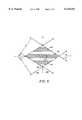
- FIG. 1is a partial front view of one embodiment of a multi-layer holographic device of the present invention.
- FIG. 2is a schematic illustrating a method of producing the multi-layer holographic device of FIG. 1.
- FIG. 3is a schematic illustrating dimensions used to calculate the number of interference fringes produced by laser beams and the spacing between the fringes.
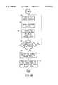
- FIG. 4Ais a flowchart illustrating a process for making the multi-layer holographic device of FIG. 1.
- FIG. 4Bis a flowchart illustrating an alternate process for making multi-layer holographic device of FIG. 1.
- FIG. 5is a schematic illustrating a switchable multi-layer holographic device.
- FIG. 6is a perspective view of a holographic optical element of the switchable multi-layer holographic device of FIG. 5 and a light source.
- FIG. 7is a partial front view of the holographic optical element of FIG. 6.
- Each layer of the holographic device 20includes a hologram which is used to control transmitted light beams based on the principles of diffraction.
- the light that passes through the hologramis diffracted by interference fringes recorded in the hologram to form an image.
- the hologramis able to perform various optical functions such as color filtering.
- the multi-layer holographic devicemay be used as a color sequential magnifier and filter which is positioned between a microdisplay and a light source to display color images.
- the holographic device 20may be used in various types of display systems including head mounted display systems, for example.
- the multi-layer holographic device 20comprises three layers of holographic material 22, 24, 26, each layer having a hologram formed therein.
- the hologramsmay be either transmissive or reflective.
- Each layer of holographic material 22, 24, 26is sensitized to red, green, or blue light.
- the layers 22, 24, 26each include a high concentration of particular dyes to ensure that each layer is sensitive to only one of the red, green, and blue colors.
- the first layer 22includes a dye which causes the layer to be sensitized to red light
- the second layer 24includes a dye that causes the layer to be sensitized to green light
- the third 26 layerincludes a dye that causes the layer to be sensitized to blue light.
- the three layers 22, 24, 26are spaced from one another with a substrate 28 interposed therebetween.
- the substrateis preferably a non-sensitized substrate such as glass, or any other suitable non-sensitized material.
- Transparent electrodesmay be deposited on opposing surfaces of the substrate which are used to encapsulate the holographic optical elements.
- the substratesmay be composed of rigid flat or curved glass, plastic or composite materials, or flexible glass, plastic, or composite materials.
- the electrodesmay be composed of transparent conducting material such as ITO or conducting polymers, for example.
- the layers 22, 24, 26are preferably between 5 and 12 microns thick and the non-sensitized substrates 28 are preferably between 0.4 and 0.8 mm thick.
- the multi-layer holographic devicemay be different than shown and described herein.
- the three holographic layersmay be positioned in a different order than shown, the multi-layer device may comprise a different number of layers, and the layers and substrates used to space the layers may have different sizes.
- the diffractive properties of the hologramdepend primarily on recorded holographic interference fringes in the holographic material of the layers 22, 24, 26.
- the holographic fringesmay be created by applying beams of light to the holographic material. As described below, the fringes may be created in the layers either sequentially using red, green, and blue laser beams in turn, or simultaneously using red, green, and blue laser beams together.
- FIG. 1illustrates the forming of a holographic interference fringe in the green-sensitized layer 24.
- Laser beams 30, 32are directed at opposite sides of the holographic device 20 and positioned to intersect at an intersection region 34.
- the laser beams 30, 32emit light consisting essentially of green wavelength bands.
- the laser beams 30, 32are oriented at an angle with respect to an incident surface of the composite structure such that the laser beams intersect one another within layer 24.
- the intensities of the laser beams 30, 32are preferably controlled such that their combined energies are slightly greater then the threshold needed to cause polymerization of the material in layer 24, while their individual energies are just below this threshold.
- the layer exposure durationmay also be used to control polymerization of the material.
- the interfering wavefronts of beams 30, 32create holographic interference fringes 36 in the layer 24 by polymerization of the green sensitized material.
- the fringesare controlled to produce the hologram by moving the laser beams 30, 32 and their intersection region 34.
- layer 24is sensitized to a green wavelength bandwidth, there may be some sensitivity of the layer to red and blue.
- the laser beams 30, 32are arranged to intersect at a volume which, although extending into the adjacent substrate 28, does not extend into the adjacent red and blue sensitized layers 22, 26.
- Red and blue laser beamsare similarly used to produce interference fringes in the layers 22, 26, respectively.
- the forming of the fringes in the layers 22, 24, 26can be done either in turn by sequentially subjecting the respective layers to red, green, and blue laser light, or simultaneously by subjecting the respective layers to red, green, and blue laser light at one time.
- FIG. 2shows one arrangement for producing the multi-layer holographic device 20 shown in FIG. 1.
- the layers 22, 24, 26, 28are stacked together to form the composite structure, it is positioned between beam shaping optics 40, 42 which are used to control profiles of the interfering wavefronts of laser beams 50, 52 at an intersection region (e.g., region 34 of FIG. 1) to create fringes with the appropriate geometry.
- the shaping optics 40, 42may include conventional optical elements such as refractive or reflective optical elements, diffraction elements, holographic elements, switchable holographic optical elements, or any combination of these elements, as is well known by those skilled in the art.
- Lasers 46, 48are positioned on opposite sides of the composite structure adjacent to the shaping optics 40, 42, respectively.
- the lasers 46, 48are positioned so that reference laser beams 50, 52 intersect at intersection region 34 (FIGS. 1 and 2).
- the lasers 46, 48are each controlled by a scanning device 60 which is operable to move the laser beams 50, 52 so that the intersection region 34 is scanned or stepped across the layer 22, 24, 26.
- the scanning devices 60are preferably controlled by a common controller 62 so that the laser beams 50, 52 are moved simultaneously and over the same distance relative to the composite structure.
- the scanning device 60may be a laser writing device used to create gratings for holographic devices, as are well known by those skilled in the art.
- the reference beams 50, 52may also be formed from a single laser beam which is split into two beams by a beam splitter (not shown) and directed to opposite sides of the intersection region 34 with a system of movable mirrors.
- FIG. 3illustrates dimensions used to calculate the number of interference fringes created within an intersection volume by a pair of laser beams and the spacing between the fringes.
- Fringes 64are shown within intersection region 65 located between laser beams 66, 68.
- the laser beams 66, 68each have a cross section dimension d and intersect at an angle 2 ⁇ (see FIG. 3).
- the spacing between fringes 5may be calculated as:
- the width D of the intersection regionis calculated as:
- the number of fringes N within intersection region 65may then be calculated as:
- FIG. 4Ais a flowchart illustrating a process for making the multi-layer holographic device 20 of FIG. 1.
- Each of the sensitized hologram layersare formed separately.
- a parallel sided thin container (bottle)comprising a pair of thin electrodes (e.g., ITO) coated glass or plastic walls separated by a narrow gap is constructed (step 70A).
- the bottleis filled with the mixture sensitized to red light (step 71A).
- the edgesare then sealed with a suitable adhesive (step 72A).
- the processis then repeated for the green and blue sensitized holograms (step 73A).
- the separate containersare then stacked to form a composite device (step 74A).
- the stackis built by starting with the substrate to which an electrode coating has already been applied (step 70B).
- a layer of holographic syrupis then deposited onto the structure (step 71B).
- the substrate layer coated with an electrode layeris added and positioned such that electrode layers on the substrate bounding the hologram are facing one another (step 72B).
- the processis then repeated to construct the second and third hologram layers (step 73B).
- the substrate separating the first and second and second and third hologram layersmay comprise two separated ITO coated substrates or alternatively a single substrate with ITO applied to both sides.
- the composite structure produced from one of the above-described methods, or other suitable methodsis placed into a retaining fixture (not shown) which is positioned between shaping optics 40, 42 (step 76) (FIGS. 2, 4A, and 4B).
- Lasers 46, 48are fixably attached to scanning devices 60 which are movable relative to the composite structure to direct laser beams 50, 52 at a region within one of the layers 22, 24, 26.
- green laser beams 30, 32are positioned to intersect at the green sensitized layer 24 and create holographic interference fringes 36 by polymerization of the sensitized material.
- the lasers 46, 48are moved by the scanning devices 60 to produce the hologram (FIG. 2).
- Red laser beamsare used to create interference fringes in the red sensitized layer 22 and blue laser beams are used to create interference fringes in the blue sensitized layer 26 (step 78).
- the lasers 46, 48may produce a laser beam which emits red, green, and blue laser light simultaneously. The different wavelengths of each color results in interference regions formed in each of the layers 22, 24, 26.
- the layers of the multi-layer holographic devicemay also be configured to be switchable between an active state and a passive state by incorporating suitable electrodes as shown in FIG. 5.
- the switchable holographic devicegenerally indicated at 80, includes three switchable holographic optical elements 82, 84, 86.
- Each holographic optical element 82, 84, 86includes a layer of holographic material sensitized to red, green, or blue light interposed between two electrode layers 88.
- the red layer 82is optimized to diffract red light
- the green layer 84is optimized to diffract green light
- the blue layer 86is optimized to diffract blue light.
- each layer 82, 84, 86may comprise a photopolymer/liquid crystal composite material such as a holographic photopoloymeric film which has been combined with liquid crystal, for example.
- the presence of the liquid crystalallows the hologram to exhibit optical characteristics which are dependent on an applied electrical field.
- the hologramselectively directs an incoming light beam from a light source 90 either towards or away from a viewer and selectively diffracts light at certain wavelengths into different modes in response to a voltage applied to the electrodes 88 (FIGS. 6 and 7).
- Light passing through the hologram in the same direction that the light is received from the light source 90is referred to as the zeroth (0th) order mode 92.
- liquid crystal droplets within the holographic optical element 82are oriented such that the hologram is present in the element and light is diffracted from the zeroth order mode to a first (1st) order mode 94 of the hologram.
- a voltageis applied to the holographic optical element 82, the liquid crystal droplets become realigned effectively erasing the hologram, and the incoming light passes through the holographic optical element in the zeroth order mode 92.
- the electrodes (electrode layers) 88are positioned on opposite sides of the holographic layer and are preferably transparent so that they do not interfere with light passing through the hologram.
- the electrodes 88may be formed from a vapor deposition of Indium Tin Oxide (ITO) which typically has a transmission efficiency of greater than 80%, or any other suitable substantially transparent conducting material. Anti-reflection coatings may be applied to the ITO such that 99% of the light incident on a single electrode will be transmitted.
- the electrodes 88are connected to an electric circuit 96 operable to apply a voltage to the electrodes, to generate an electric field (FIG. 7).
- the hologramis in the diffractive (active) state and the holographic optical element 82 diffracts propagating light in a predefined manner.
- the electrodes 88may be different than described herein. For example, a plurality of smaller electrodes may be used rather than two large electrodes which substantially cover surfaces of the holograms.
- a voltage controller(not shown) operates to sequentially display three monochromatic images of the color input image.
- the electrodes 88 attached to each of the holograms 82, 84, 86are sequentially enabled such that a selected amount of red, green, and blue light is directed towards the viewer. For example, when a red monochromatic image is projected, the voltage controller switches the green and blue holograms 84, 86 to the passive state by applying voltages to their respective electrodes 88.
- the supplied voltages to the electrodes 88 of the green and blue holograms 84, 86create a potential difference between the electrodes, thereby generating an electrical field within the green and blue holograms.
- the presence of the generated electrical fieldswitches the optical characteristic of the holograms 84, 86 to the passive state.
- the green and blue holograms 84, 86 in the passive state and the red hologram 82 in the diffractive stateonly the red hologram optically diffracts the projected red image. Thus, only the portion of the visible light spectrum corresponding to the red light is diffracted to the viewer.
- the green hologram 84is next changed to the diffractive state by deenergizing the corresponding electrodes 88 and the electrodes of the red hologram 82 are energized to change the red hologram to the passive state so that only green light is diffracted.
- the blue hologram 86is then changed to the diffractive state by deenergizing its electrodes 88 and the electrodes of the green hologram 84 are energized to change the green hologram to the passive state so that only blue light is diffracted.
- the hologramsare sequentially enabled with a refresh rate which is faster than the response time of a human eye so that a color image will be created in the viewer's eye due to the integration of the red, green, and blue monochrome images created from each of the red, green, and blue holograms. Consequently, the holographic devices will be illuminated sequentially by red, green, and blue lights so that the final viewable image will appear to be displayed as a composite color.
- the red, green, and blue holographic elements 82, 84, 86may be cycled on and off in any order.
- the multi-layer hologrammay also be formed with non-planar layers.
- the layersmay each have aligned curved surfaces to project a pre-distorted image which can be used to correct distortion typically present in an image projected from a flat image display (see e.g., U.S. patent application entitled Holographic Display System, by M. Popovich, Ser. No. 09/416,076, filed Oct. 12, 1999).
- the multi-layer holographic device and method of making disclosed hereinhave many advantages.
- the multi-layer deviceenables holograms to be created in layers which are already stacked in a composite holographic structure.
- the method described above for forming the multilayer deviceavoids the problems of alignment associated with holograms created in individual layers and later stacked together.
- the methodallows for simplification of the recording optics, since the wavefront shape of the laser beams needs only to match the local geometry of the hologram.
- the methodalso allows for matching of the polarization of the recording laser beams to the required polarization characteristics of the hologram.
Landscapes
- Physics & Mathematics (AREA)
- General Physics & Mathematics (AREA)
- Holo Graphy (AREA)
Abstract
Description
S=λ/[2 sin θ].
D=d/[cos θ].
N=D/S=(2d/λ)[tan θ].
Claims (27)
Priority Applications (3)
| Application Number | Priority Date | Filing Date | Title |
|---|---|---|---|
| US09/469,712US6115151A (en) | 1998-12-30 | 1999-12-21 | Method for producing a multi-layer holographic device |
| PCT/US1999/031268WO2000039641A1 (en) | 1998-12-30 | 1999-12-29 | Method for producing a multi-layer holographic device |
| AU24872/00AAU2487200A (en) | 1998-12-30 | 1999-12-29 | Method for producing a multi-layer holographic device |
Applications Claiming Priority (2)
| Application Number | Priority Date | Filing Date | Title |
|---|---|---|---|
| US11417698P | 1998-12-30 | 1998-12-30 | |
| US09/469,712US6115151A (en) | 1998-12-30 | 1999-12-21 | Method for producing a multi-layer holographic device |
Publications (1)
| Publication Number | Publication Date |
|---|---|
| US6115151Atrue US6115151A (en) | 2000-09-05 |
Family
ID=26811885
Family Applications (1)
| Application Number | Title | Priority Date | Filing Date |
|---|---|---|---|
| US09/469,712Expired - Fee RelatedUS6115151A (en) | 1998-12-30 | 1999-12-21 | Method for producing a multi-layer holographic device |
Country Status (3)
| Country | Link |
|---|---|
| US (1) | US6115151A (en) |
| AU (1) | AU2487200A (en) |
| WO (1) | WO2000039641A1 (en) |
Cited By (18)
| Publication number | Priority date | Publication date | Assignee | Title |
|---|---|---|---|---|
| US20020158866A1 (en)* | 2000-10-20 | 2002-10-31 | Batchko Robert G. | Combinatorial optical processor |
| US6577291B2 (en)* | 1998-10-07 | 2003-06-10 | Microsoft Corporation | Gray scale and color display methods and apparatus |
| US6651886B2 (en) | 2001-04-13 | 2003-11-25 | Symbol Technologies, Inc. | Optical code readers with holographic optical elements |
| US20040008208A1 (en)* | 1999-02-01 | 2004-01-15 | Bodin Dresevic | Quality of displayed images with user preference information |
| US20040114203A1 (en)* | 2001-10-19 | 2004-06-17 | Batchko Robert G. | Digital focus lens system |
| US6780546B2 (en) | 2001-08-30 | 2004-08-24 | Inphase Technologies, Inc. | Blue-sensitized holographic media |
| US6950103B2 (en) | 1998-10-07 | 2005-09-27 | Microsoft Corporation | Automatic optimization of the position of stems of text characters |
| US20050237589A1 (en)* | 2003-09-23 | 2005-10-27 | Sbg Labs, Inc. | Optical filter employing holographic optical elements and image generating system incorporating the optical filter |
| US20060034603A1 (en)* | 2002-12-06 | 2006-02-16 | Nikon Corporation | Holographic optical device, camera finder indication, and camera |
| US7006425B1 (en)* | 1998-11-30 | 2006-02-28 | Kabushiki Kaisha Toshiba | Information recording and/or reproducing method and apparatus for three dimensional optical recording medium |
| US20060251989A1 (en)* | 2005-05-09 | 2006-11-09 | International Business Machines Corporation | Photoresists for visible light imaging |
| US20070148466A1 (en)* | 2004-02-12 | 2007-06-28 | Toru Iwane | Multilayer film optical member and method for manufacturing multilayer film optical member |
| US20150205261A1 (en)* | 2012-08-17 | 2015-07-23 | Artience Lab Inc. | Illumination device and image recording medium |
| US20200356050A1 (en)* | 2019-05-08 | 2020-11-12 | Facebook Technologies, Llc | Spatial deposition of resins with different functionality |
| JP2021033172A (en)* | 2019-08-28 | 2021-03-01 | セイコーエプソン株式会社 | Manufacturing method of optical element, optical element and display device |
| USD918654S1 (en) | 2019-06-06 | 2021-05-11 | Sharkninja Operating Llc | Grill plate |
| US11656458B2 (en) | 2019-01-23 | 2023-05-23 | Fusao Ishii | Optics of a display using an optical light guide |
| US11789186B1 (en) | 2018-01-23 | 2023-10-17 | Meta Platforms Technologies, Llc | Diffraction grating with a variable refractive index formed using an energy gradient |
Citations (17)
| Publication number | Priority date | Publication date | Assignee | Title |
|---|---|---|---|---|
| US3807829A (en)* | 1973-04-30 | 1974-04-30 | Hughes Aircraft Co | Extended-field holographic lens arrays |
| US4790613A (en)* | 1987-01-06 | 1988-12-13 | Hughes Aircraft Company | Holographic display panel for a vehicle windshield |
| US4932731A (en)* | 1986-11-14 | 1990-06-12 | Yazaki Corporation | Holographic head-up display apparatus |
| US4981332A (en)* | 1989-06-29 | 1991-01-01 | Hughes Aircraft Company | Dispersion-compensated windshield hologram virtual image display |
| US5035474A (en)* | 1984-04-16 | 1991-07-30 | Hughes Aircraft Company | Biocular holographic helmet mounted display |
| US5044709A (en)* | 1988-11-30 | 1991-09-03 | Hughes Aircraft Company | LED array polarized image source/0 degree hologram virtual image head up display |
| US5151724A (en)* | 1991-01-30 | 1992-09-29 | Dan Kikinis | Dynamic holographic display with cantilever |
| US5278532A (en)* | 1987-09-14 | 1994-01-11 | Hughes Aircraft Company | Automotive instrument virtual image display |
| US5305124A (en)* | 1992-04-07 | 1994-04-19 | Hughes Aircraft Company | Virtual image display system |
| US5424866A (en)* | 1991-01-30 | 1995-06-13 | Kikinis; Dan | Dynamic holographic display with cantilever |
| US5440428A (en)* | 1993-09-30 | 1995-08-08 | Hughes Aircraft Company | Automotive instrument 3-D virtual image display |
| US5537232A (en)* | 1993-10-05 | 1996-07-16 | In Focus Systems, Inc. | Reflection hologram multiple-color filter array formed by sequential exposure to a light source |
| US5550701A (en)* | 1994-08-30 | 1996-08-27 | International Rectifier Corporation | Power MOSFET with overcurrent and over-temperature protection and control circuit decoupled from body diode |
| US5569565A (en)* | 1991-05-23 | 1996-10-29 | Matsushita Electric Industrial Co., Ltd. | Hologram recording material |
| US5581378A (en)* | 1993-02-01 | 1996-12-03 | University Of Alabama At Huntsville | Electro-optical holographic display |
| US5680231A (en)* | 1995-06-06 | 1997-10-21 | Hughes Aircraft Company | Holographic lenses with wide angular and spectral bandwidths for use in a color display device |
| US5703702A (en)* | 1993-09-08 | 1997-12-30 | Crane; Patrick E. | Holographic synthesis |
- 1999
- 1999-12-21USUS09/469,712patent/US6115151A/ennot_activeExpired - Fee Related
- 1999-12-29WOPCT/US1999/031268patent/WO2000039641A1/enactiveApplication Filing
- 1999-12-29AUAU24872/00Apatent/AU2487200A/ennot_activeAbandoned
Patent Citations (17)
| Publication number | Priority date | Publication date | Assignee | Title |
|---|---|---|---|---|
| US3807829A (en)* | 1973-04-30 | 1974-04-30 | Hughes Aircraft Co | Extended-field holographic lens arrays |
| US5035474A (en)* | 1984-04-16 | 1991-07-30 | Hughes Aircraft Company | Biocular holographic helmet mounted display |
| US4932731A (en)* | 1986-11-14 | 1990-06-12 | Yazaki Corporation | Holographic head-up display apparatus |
| US4790613A (en)* | 1987-01-06 | 1988-12-13 | Hughes Aircraft Company | Holographic display panel for a vehicle windshield |
| US5278532A (en)* | 1987-09-14 | 1994-01-11 | Hughes Aircraft Company | Automotive instrument virtual image display |
| US5044709A (en)* | 1988-11-30 | 1991-09-03 | Hughes Aircraft Company | LED array polarized image source/0 degree hologram virtual image head up display |
| US4981332A (en)* | 1989-06-29 | 1991-01-01 | Hughes Aircraft Company | Dispersion-compensated windshield hologram virtual image display |
| US5151724A (en)* | 1991-01-30 | 1992-09-29 | Dan Kikinis | Dynamic holographic display with cantilever |
| US5424866A (en)* | 1991-01-30 | 1995-06-13 | Kikinis; Dan | Dynamic holographic display with cantilever |
| US5569565A (en)* | 1991-05-23 | 1996-10-29 | Matsushita Electric Industrial Co., Ltd. | Hologram recording material |
| US5305124A (en)* | 1992-04-07 | 1994-04-19 | Hughes Aircraft Company | Virtual image display system |
| US5581378A (en)* | 1993-02-01 | 1996-12-03 | University Of Alabama At Huntsville | Electro-optical holographic display |
| US5703702A (en)* | 1993-09-08 | 1997-12-30 | Crane; Patrick E. | Holographic synthesis |
| US5440428A (en)* | 1993-09-30 | 1995-08-08 | Hughes Aircraft Company | Automotive instrument 3-D virtual image display |
| US5537232A (en)* | 1993-10-05 | 1996-07-16 | In Focus Systems, Inc. | Reflection hologram multiple-color filter array formed by sequential exposure to a light source |
| US5550701A (en)* | 1994-08-30 | 1996-08-27 | International Rectifier Corporation | Power MOSFET with overcurrent and over-temperature protection and control circuit decoupled from body diode |
| US5680231A (en)* | 1995-06-06 | 1997-10-21 | Hughes Aircraft Company | Holographic lenses with wide angular and spectral bandwidths for use in a color display device |
Cited By (30)
| Publication number | Priority date | Publication date | Assignee | Title |
|---|---|---|---|---|
| US6950103B2 (en) | 1998-10-07 | 2005-09-27 | Microsoft Corporation | Automatic optimization of the position of stems of text characters |
| US6577291B2 (en)* | 1998-10-07 | 2003-06-10 | Microsoft Corporation | Gray scale and color display methods and apparatus |
| US7006425B1 (en)* | 1998-11-30 | 2006-02-28 | Kabushiki Kaisha Toshiba | Information recording and/or reproducing method and apparatus for three dimensional optical recording medium |
| US20040008208A1 (en)* | 1999-02-01 | 2004-01-15 | Bodin Dresevic | Quality of displayed images with user preference information |
| US7134091B2 (en) | 1999-02-01 | 2006-11-07 | Microsoft Corporation | Quality of displayed images with user preference information |
| US20090284489A1 (en)* | 2000-10-20 | 2009-11-19 | Batchko Robert G | Multiplanar volumetric three-dimensional display apparatus |
| US20020158866A1 (en)* | 2000-10-20 | 2002-10-31 | Batchko Robert G. | Combinatorial optical processor |
| US7218429B2 (en) | 2000-10-20 | 2007-05-15 | Batchko Robert G | Digital focus lens system |
| US8854423B2 (en) | 2000-10-20 | 2014-10-07 | Robert G. Batchko | Multiplanar volumetric three-dimensional display apparatus |
| US20060114534A1 (en)* | 2000-10-20 | 2006-06-01 | Batchko Robert G | Digital focus lens system |
| US7218430B2 (en) | 2000-10-20 | 2007-05-15 | Robert G Batchko | Combinatorial optical processor |
| US6651886B2 (en) | 2001-04-13 | 2003-11-25 | Symbol Technologies, Inc. | Optical code readers with holographic optical elements |
| US6780546B2 (en) | 2001-08-30 | 2004-08-24 | Inphase Technologies, Inc. | Blue-sensitized holographic media |
| US20040114203A1 (en)* | 2001-10-19 | 2004-06-17 | Batchko Robert G. | Digital focus lens system |
| US7072086B2 (en) | 2001-10-19 | 2006-07-04 | Batchko Robert G | Digital focus lens system |
| US20060034603A1 (en)* | 2002-12-06 | 2006-02-16 | Nikon Corporation | Holographic optical device, camera finder indication, and camera |
| US7426343B2 (en) | 2002-12-06 | 2008-09-16 | Nikon Corporation | Holographic optical device, camera finder indication, and camera |
| US20050237589A1 (en)* | 2003-09-23 | 2005-10-27 | Sbg Labs, Inc. | Optical filter employing holographic optical elements and image generating system incorporating the optical filter |
| US20070148466A1 (en)* | 2004-02-12 | 2007-06-28 | Toru Iwane | Multilayer film optical member and method for manufacturing multilayer film optical member |
| US20080166669A1 (en)* | 2005-05-09 | 2008-07-10 | International Business Machines Corporation | Photoresists for Visible Light Imaging |
| US7354692B2 (en) | 2005-05-09 | 2008-04-08 | International Business Machines Corporation | Photoresists for visible light imaging |
| US7807340B2 (en) | 2005-05-09 | 2010-10-05 | International Business Machines Corporation | Photoresists for visible light imaging |
| US20060251989A1 (en)* | 2005-05-09 | 2006-11-09 | International Business Machines Corporation | Photoresists for visible light imaging |
| US20150205261A1 (en)* | 2012-08-17 | 2015-07-23 | Artience Lab Inc. | Illumination device and image recording medium |
| US9915921B2 (en)* | 2012-08-17 | 2018-03-13 | Artience Lab Inc. | Illumination device and image recording medium |
| US11789186B1 (en) | 2018-01-23 | 2023-10-17 | Meta Platforms Technologies, Llc | Diffraction grating with a variable refractive index formed using an energy gradient |
| US11656458B2 (en) | 2019-01-23 | 2023-05-23 | Fusao Ishii | Optics of a display using an optical light guide |
| US20200356050A1 (en)* | 2019-05-08 | 2020-11-12 | Facebook Technologies, Llc | Spatial deposition of resins with different functionality |
| USD918654S1 (en) | 2019-06-06 | 2021-05-11 | Sharkninja Operating Llc | Grill plate |
| JP2021033172A (en)* | 2019-08-28 | 2021-03-01 | セイコーエプソン株式会社 | Manufacturing method of optical element, optical element and display device |
Also Published As
| Publication number | Publication date |
|---|---|
| WO2000039641A1 (en) | 2000-07-06 |
| AU2487200A (en) | 2000-07-31 |
Similar Documents
| Publication | Publication Date | Title |
|---|---|---|
| US12298513B2 (en) | Waveguide device with uniform output illumination | |
| US11573483B2 (en) | Systems and methods for multiplying the image resolution of a pixelated display | |
| US12140764B2 (en) | Wide angle waveguide display | |
| US11543594B2 (en) | Methods and apparatuses for providing a holographic waveguide display using integrated gratings | |
| US11378732B2 (en) | Holographic waveguide backlight and related methods of manufacturing | |
| US6646636B1 (en) | Display system utilizing ambient light and a dedicated light source | |
| US6115151A (en) | Method for producing a multi-layer holographic device | |
| JP2022091982A (en) | Waveguide with uniform output illumination | |
| US6185016B1 (en) | System for generating an image | |
| US6373603B1 (en) | Image generating system including compensation for chromatic dispersion | |
| US20010024177A1 (en) | Holographic display system | |
| JP2019512745A (en) | Method and apparatus for providing polarization selective holographic waveguide device | |
| US6643039B1 (en) | Holographic reflector and reflectiver liquid crystal display using it | |
| WO2000068715A1 (en) | Image generating system | |
| WO2000043841A9 (en) | System for generating images using switchable holographic optical elements | |
| WO2000049431A1 (en) | Optical filter system |
Legal Events
| Date | Code | Title | Description |
|---|---|---|---|
| AS | Assignment | Owner name:DIGILENS, INC., CALIFORNIA Free format text:ASSIGNMENT OF ASSIGNORS INTEREST;ASSIGNOR:POPOVICH, MILAN M.;REEL/FRAME:010654/0049 Effective date:20000221 | |
| AS | Assignment | Owner name:GATX VENTURES, INC., AS AGENT, CALIFORNIA Free format text:SECURITY INTEREST;ASSIGNOR:DIGILENS, INC.;REEL/FRAME:011763/0146 Effective date:20010424 Owner name:GATX VENTURES, INC., CALIFORNIA Free format text:SECURITY INTEREST;ASSIGNOR:DIGILENS, INC.;REEL/FRAME:011763/0156 Effective date:20010424 Owner name:TRANSAMERICA BUSINESS CREDIT CORPORATION, CONNECTI Free format text:SECURITY INTEREST;ASSIGNOR:DIGILENS, INC.;REEL/FRAME:011763/0156 Effective date:20010424 | |
| AS | Assignment | Owner name:HOYA CORPORATION, JAPAN Free format text:ASSIGNMENT OF ASSIGNORS INTEREST;ASSIGNOR:SBG LABS, INC.;REEL/FRAME:014101/0471 Effective date:20031031 Owner name:SBG LABS, INC., CALIFORNIA Free format text:ASSIGNMENT OF ASSIGNORS INTEREST;ASSIGNORS:GATX, VENTURES, INC.;GATX VENTURES, INC., AS AGENT;TRANSAMERICA BUSINESS CREDIT CORPORATION;REEL/FRAME:014101/0406 Effective date:20031016 | |
| REMI | Maintenance fee reminder mailed | ||
| FPAY | Fee payment | Year of fee payment:4 | |
| SULP | Surcharge for late payment | ||
| REMI | Maintenance fee reminder mailed | ||
| LAPS | Lapse for failure to pay maintenance fees | ||
| STCH | Information on status: patent discontinuation | Free format text:PATENT EXPIRED DUE TO NONPAYMENT OF MAINTENANCE FEES UNDER 37 CFR 1.362 | |
| FP | Lapsed due to failure to pay maintenance fee | Effective date:20080905 |