US6114211A - Semiconductor device with vertical halo region and methods of manufacture - Google Patents
Semiconductor device with vertical halo region and methods of manufactureDownload PDFInfo
- Publication number
- US6114211A US6114211AUS09/195,336US19533698AUS6114211AUS 6114211 AUS6114211 AUS 6114211AUS 19533698 AUS19533698 AUS 19533698AUS 6114211 AUS6114211 AUS 6114211A
- Authority
- US
- United States
- Prior art keywords
- spacer
- forming
- substrate
- dopant material
- gate electrode
- Prior art date
- Legal status (The legal status is an assumption and is not a legal conclusion. Google has not performed a legal analysis and makes no representation as to the accuracy of the status listed.)
- Expired - Lifetime
Links
- 238000000034methodMethods0.000titleclaimsabstractdescription64
- 239000004065semiconductorSubstances0.000titleclaimsabstractdescription30
- 125000001475halogen functional groupChemical group0.000titleclaimsabstract20
- 238000004519manufacturing processMethods0.000titledescription8
- 125000006850spacer groupChemical group0.000claimsabstractdescription126
- 239000002019doping agentSubstances0.000claimsabstractdescription123
- 239000000463materialSubstances0.000claimsabstractdescription109
- 239000000758substrateSubstances0.000claimsabstractdescription65
- 239000010410layerSubstances0.000claimsdescription90
- 238000002513implantationMethods0.000claimsdescription13
- 239000011241protective layerSubstances0.000claimsdescription6
- VYPSYNLAJGMNEJ-UHFFFAOYSA-NSilicium dioxideChemical compoundO=[Si]=OVYPSYNLAJGMNEJ-UHFFFAOYSA-N0.000abstractdescription23
- 230000015572biosynthetic processEffects0.000abstractdescription22
- 239000000377silicon dioxideSubstances0.000abstractdescription11
- 235000012239silicon dioxideNutrition0.000abstractdescription9
- 229910052581Si3N4Inorganic materials0.000abstractdescription4
- HQVNEWCFYHHQES-UHFFFAOYSA-Nsilicon nitrideChemical compoundN12[Si]34N5[Si]62N3[Si]51N64HQVNEWCFYHHQES-UHFFFAOYSA-N0.000abstractdescription4
- 230000008021depositionEffects0.000abstractdescription2
- 125000005843halogen groupChemical group0.000description31
- 239000007943implantSubstances0.000description20
- 125000004429atomChemical group0.000description14
- 239000003989dielectric materialSubstances0.000description7
- XUIMIQQOPSSXEZ-UHFFFAOYSA-NSiliconChemical compound[Si]XUIMIQQOPSSXEZ-UHFFFAOYSA-N0.000description6
- 230000005684electric fieldEffects0.000description6
- -1for exampleSubstances0.000description6
- 238000012545processingMethods0.000description6
- 229910052710siliconInorganic materials0.000description6
- 239000010703siliconSubstances0.000description6
- 238000005229chemical vapour depositionMethods0.000description5
- 238000012986modificationMethods0.000description5
- 230000004048modificationEffects0.000description5
- 230000000873masking effectEffects0.000description4
- 238000005240physical vapour depositionMethods0.000description4
- 229910021420polycrystalline siliconInorganic materials0.000description4
- 229920005591polysiliconPolymers0.000description4
- 239000000126substanceSubstances0.000description4
- 229910052796boronInorganic materials0.000description3
- 238000005530etchingMethods0.000description3
- 238000010438heat treatmentMethods0.000description3
- 239000012535impuritySubstances0.000description3
- 229910052751metalInorganic materials0.000description3
- 239000002184metalSubstances0.000description3
- 238000005498polishingMethods0.000description3
- ZOXJGFHDIHLPTG-UHFFFAOYSA-NBoronChemical compound[B]ZOXJGFHDIHLPTG-UHFFFAOYSA-N0.000description2
- BOTDANWDWHJENH-UHFFFAOYSA-NTetraethyl orthosilicateChemical compoundCCO[Si](OCC)(OCC)OCCBOTDANWDWHJENH-UHFFFAOYSA-N0.000description2
- 229910052785arsenicInorganic materials0.000description2
- RQNWIZPPADIBDY-UHFFFAOYSA-Narsenic atomChemical compound[As]RQNWIZPPADIBDY-UHFFFAOYSA-N0.000description2
- 238000007796conventional methodMethods0.000description2
- 238000000151depositionMethods0.000description2
- 238000005516engineering processMethods0.000description2
- 230000003647oxidationEffects0.000description2
- 238000007254oxidation reactionMethods0.000description2
- 239000002356single layerSubstances0.000description2
- RYGMFSIKBFXOCR-UHFFFAOYSA-NCopperChemical compound[Cu]RYGMFSIKBFXOCR-UHFFFAOYSA-N0.000description1
- OAICVXFJPJFONN-UHFFFAOYSA-NPhosphorusChemical compound[P]OAICVXFJPJFONN-UHFFFAOYSA-N0.000description1
- RTAQQCXQSZGOHL-UHFFFAOYSA-NTitaniumChemical compound[Ti]RTAQQCXQSZGOHL-UHFFFAOYSA-N0.000description1
- 229910052782aluminiumInorganic materials0.000description1
- XAGFODPZIPBFFR-UHFFFAOYSA-NaluminiumChemical compound[Al]XAGFODPZIPBFFR-UHFFFAOYSA-N0.000description1
- QVGXLLKOCUKJST-UHFFFAOYSA-Natomic oxygenChemical group[O]QVGXLLKOCUKJST-UHFFFAOYSA-N0.000description1
- UORVGPXVDQYIDP-UHFFFAOYSA-NboraneChemical compoundBUORVGPXVDQYIDP-UHFFFAOYSA-N0.000description1
- 229910010277boron hydrideInorganic materials0.000description1
- 239000000969carrierSubstances0.000description1
- 238000004891communicationMethods0.000description1
- 239000004020conductorSubstances0.000description1
- 229910052802copperInorganic materials0.000description1
- 239000010949copperSubstances0.000description1
- 238000009792diffusion processMethods0.000description1
- 238000009826distributionMethods0.000description1
- 230000000694effectsEffects0.000description1
- 239000011521glassSubstances0.000description1
- BHEPBYXIRTUNPN-UHFFFAOYSA-Nhydridophosphorus(.) (triplet)Chemical compound[PH]BHEPBYXIRTUNPN-UHFFFAOYSA-N0.000description1
- 238000009413insulationMethods0.000description1
- 230000010354integrationEffects0.000description1
- 150000002739metalsChemical class0.000description1
- 229910052757nitrogenChemical group0.000description1
- IJGRMHOSHXDMSA-UHFFFAOYSA-NnitrogenChemical groupN#NIJGRMHOSHXDMSA-UHFFFAOYSA-N0.000description1
- QJGQUHMNIGDVPM-UHFFFAOYSA-Nnitrogen groupChemical group[N]QJGQUHMNIGDVPM-UHFFFAOYSA-N0.000description1
- 229910052698phosphorusInorganic materials0.000description1
- 239000011574phosphorusSubstances0.000description1
- 229920002120photoresistant polymerPolymers0.000description1
- 238000012552reviewMethods0.000description1
- 238000000926separation methodMethods0.000description1
- 229910052814silicon oxideInorganic materials0.000description1
- 239000010936titaniumSubstances0.000description1
- 229910052719titaniumInorganic materials0.000description1
- WFKWXMTUELFFGS-UHFFFAOYSA-NtungstenChemical compound[W]WFKWXMTUELFFGS-UHFFFAOYSA-N0.000description1
- 229910052721tungstenInorganic materials0.000description1
- 239000010937tungstenSubstances0.000description1
- 238000009827uniform distributionMethods0.000description1
Images


Classifications
- H—ELECTRICITY
- H10—SEMICONDUCTOR DEVICES; ELECTRIC SOLID-STATE DEVICES NOT OTHERWISE PROVIDED FOR
- H10D—INORGANIC ELECTRIC SEMICONDUCTOR DEVICES
- H10D30/00—Field-effect transistors [FET]
- H10D30/01—Manufacture or treatment
- H10D30/021—Manufacture or treatment of FETs having insulated gates [IGFET]
- H10D30/022—Manufacture or treatment of FETs having insulated gates [IGFET] having lightly-doped source or drain extensions selectively formed at the sides of the gates
- H—ELECTRICITY
- H10—SEMICONDUCTOR DEVICES; ELECTRIC SOLID-STATE DEVICES NOT OTHERWISE PROVIDED FOR
- H10D—INORGANIC ELECTRIC SEMICONDUCTOR DEVICES
- H10D30/00—Field-effect transistors [FET]
- H10D30/01—Manufacture or treatment
- H10D30/021—Manufacture or treatment of FETs having insulated gates [IGFET]
- H10D30/0223—Manufacture or treatment of FETs having insulated gates [IGFET] having source and drain regions or source and drain extensions self-aligned to sides of the gate
- H10D30/0227—Manufacture or treatment of FETs having insulated gates [IGFET] having source and drain regions or source and drain extensions self-aligned to sides of the gate having both lightly-doped source and drain extensions and source and drain regions self-aligned to the sides of the gate, e.g. lightly-doped drain [LDD] MOSFET or double-diffused drain [DDD] MOSFET
- H—ELECTRICITY
- H10—SEMICONDUCTOR DEVICES; ELECTRIC SOLID-STATE DEVICES NOT OTHERWISE PROVIDED FOR
- H10D—INORGANIC ELECTRIC SEMICONDUCTOR DEVICES
- H10D62/00—Semiconductor bodies, or regions thereof, of devices having potential barriers
- H10D62/10—Shapes, relative sizes or dispositions of the regions of the semiconductor bodies; Shapes of the semiconductor bodies
- H10D62/17—Semiconductor regions connected to electrodes not carrying current to be rectified, amplified or switched, e.g. channel regions
- H10D62/351—Substrate regions of field-effect devices
- H10D62/357—Substrate regions of field-effect devices of FETs
- H10D62/364—Substrate regions of field-effect devices of FETs of IGFETs
- H10D62/371—Inactive supplementary semiconductor regions, e.g. for preventing punch-through, improving capacity effect or leakage current
- H—ELECTRICITY
- H10—SEMICONDUCTOR DEVICES; ELECTRIC SOLID-STATE DEVICES NOT OTHERWISE PROVIDED FOR
- H10D—INORGANIC ELECTRIC SEMICONDUCTOR DEVICES
- H10D64/00—Electrodes of devices having potential barriers
- H10D64/01—Manufacture or treatment
- H10D64/015—Manufacture or treatment removing at least parts of gate spacers, e.g. disposable spacers
Definitions
- the present inventionis directed to semiconductor devices and method of making these devices.
- the present inventionis directed to semiconductor devices having a vertical halo region below a lightly-doped drain region and adjacent to an active region and methods of making these devices.
- MOSmetal-oxide-semiconductor
- a typical MOS semiconductor devicegenerally includes a semiconductor substrate on which a gate electrode is disposed.
- the gate electrodewhich acts as a conductor, receives an input signal to control operation of the device.
- Source and drain regionsare typically formed in regions of the substrate adjacent to the gate electrodes by heavily doping the regions with a dopant material of a desired conductivity. The conductivity of the doped region depends on the type and concentration of the impurity used to dope the region.
- the typical MOS transistoris symmetrical, which means that the source and drain are interchangeable. Whether a region acts as a source or drain typically depends on the respective applied voltages and the type of device being made.
- the collective term source/drain regionis used herein to generally describe an active region used for the formation of either a source or drain.
- a channel regionis formed in the semiconductor substrate beneath the gate electrode and between the source and drain regions.
- the channelis typically lightly-doped with a dopant material.
- the gate electrodeis generally separated from the substrate by an insulating layer, typically an oxide layer such as SiO 2 .
- the insulating layeris provided to prevent current from flowing between the gate electrode and the source, drain or channel regions.
- a voltageis typically developed between the source and drain terminals.
- a transverse electric fieldis set up in the channel region. By varying the transverse electric field, it is possible to modulate the conductance of the channel region between the source and drain regions. In this manner, an electric field is used to control the current flow through the channel region.
- This type of deviceis commonly referred to as a MOS field-effect-transistor (MOSFET).
- MOS devicestypically fall in one of two groups depending on the type of dopant materials used to form the source, drain and channel regions.
- the two groupsare often referred to as n-channel and p-channel devices.
- the type of channelis identified based on the conductivity type of the channel which is developed under the transverse electric field.
- NMOSn-channel MOS
- PMOSp-channel MOS
- p-type impuritiese.g., boron
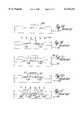
- MOS devicesA number of different techniques and fabrication processes may be used to form MOS devices. With reference to FIGS. 1A-1E, one typical MOS fabrication process is depicted to form semiconductor structures with source/drain structures having heavily-doped regions and adjacent lightly-doped regions commonly referred to as lightly-doped drain (LDD) regions. LDD structures are often used in the formation of semiconductor devices having short channels to prevent or reduce short-channel effects.
- LDDlightly-doped drain
- a gate electrode 103is formed on a substrate 101.
- An LDD region 115is formed in the substrate 101 by implanting a relatively low dose of a dopant material 110 into the exposed areas, as illustrated in FIG. 1B.
- a spacer layer 116is formed and etched to form spacers 117 on sidewalls of the gate electrode 103, as illustrated in FIGS. 1C and 1D.
- the substrate 101is again implanted with a heavy dose of dopant material 120 aligned with the spacers 117 to form heavily-doped regions 118, which together with the LDD regions 115, form LDD source/drain structures 119, as illustrated in FIG. 1E.
- LDD structures 119Following formation of the LDD structures 119, further processing such as silicidation and interconnect formation is performed. A more detailed description of the elements and fabrication of source/drain structures may be found in S. Wolf, Silicon Processing for the VLSI Era, Vol. 2: Processing Integration, pp. 354-363.
- One problem of short channel junctionsis punchthrough of carriers across the channel region from one heavily-doped region to the other in the absence of a gate current Punchthrough typically occurs due to the merging of the source and drain depletion areas.
- a variety of punchthrough implant techniqueshave been developed to overcome this problem. These include providing a punchthrough implant in the channel region prior to formation of the gate electrode.
- An alternative methodincludes forming a halo region adjacent to the heavily-doped active regions of the source/drain structures and below the LDD region using, for example, an angled implant of a dopant material having a different conductivity type than that of the heavily-doped regions and LDD regions.
- This halo regionis typically formed after the heavily-doped and LDD regions. See, for example, S. Wolf, Silicon Processing for the VLSI Era, Vol. 3: The Submicron MOSFET, pp. 238-240, 309-311, and 621-22. As semiconductor devices become smaller, there is a need for methods that provide for greater precision in the alignment of structures in a device, including the heavily-doped, LDD, and halo regions, to ensure accurate and reproducible device structures.
- the present inventionrelates to the formation of, as well as devices containing, a halo region below a lightly-doped region and adjacent to a lower portion of an active region to, at least in part, prevent or reduce punchthrough.
- the present inventionrelates to the formation of, as well as devices containing, a halo region vertically disposed below the lightly-doped region.
- One method of forming a semiconductor deviceincludes forming a gate electrode on a substrate and then forming a spacer adjacent to a sidewall of the gate electrode.
- An active regionis formed in the substrate adjacent to the spacer and spaced apart from the gate electrode using a first dopant material of a first conductivity type.
- a protecting layeris formed over the active region and adjacent to the spacer. At least a portion of the spacer is then removed to form an opening between the protecting layer and the gate electrode.
- the spacermay be formed by independent deposition of two different materials (e.g., silicon nitride and silicon dioxide), one of which can be selectively removed with respect to the other.
- a lightly-doped regionis formed in the substrate adjacent to the gate electrode using a second dopant material of the first conductivity type.
- This lightly-doped regionmay be formed, for example, prior to formation of the spacer, between the formation of two portions of the spacer, or after removing at least a portion of the spacer.
- a halo regionis formed through the opening resulting from removing a portion of the spacer.
- the halo regionis deeper in the substrate than the lightly-doped region and is adjacent to the active region.
- the halo regionis formed using a third dopant material of a conductivity type different than the first conductivity type.
- a second halo regionmay optionally be formed by implanting a fourth dopant material beneath the first halo region.
- a semiconductor deviceincludes a substrate and a gate electrode over the substrate.
- a lightly-doped regionis in the substrate adjacent to the gate electrode and a heavily-doped active region is in the substrate adjacent to the lightly-doped active region.
- a first halo regionis vertically disposed below the lightly-doped region and adjacent to the heavily-doped region.
- a second halo regionis vertically disposed below the first halo region.
- the first and second halo regionsare doped with a material of a conductivity type different than material used to dope the lightly-doped region and heavily-doped active region.
- FIGS. 1A through 1Eillustrate a conventional process for forming a semiconductor device
- FIGS. 2A through 2Iillustrate an exemplary fabrication process for forming a semiconductor device in accordance with one embodiment of the invention.
- FIGS. 3A through 3Hillustrate an exemplary fabrication process for forming a semiconductor device in accordance with another embodiment of the invention.
- the present inventionis believed to be applicable to semiconductor devices and their formation.
- the inventionis particularly suited for the formation of semiconductor devices with self-aligned heavily-doped active, LDD (lightly-doped drain), and halo regions. While the present invention is not so limited, an appreciation of various aspects of the invention will be gained through a discussion of the various application examples operating in such environments.
- FIGS. 2A through 2Iillustrate one example of a method for forming a semiconductor device according to the invention.
- a gate electrode 204is formed over a substrate 200 and a gate insulating layer 202, as shown in FIG. 2A.
- the substrate 200is typically a semiconductor material and can be, for example, silicon.
- the gate insulating layer 202can be made using a variety of dielectric materials including, for example, silicon dioxide (SiO 2 ) and silicon oxynitride (SiO x N y ). Other dielectric materials may be used for the gate insulating layer.
- the gate insulating layercan be made by a variety of methods including, for example, thermal oxidation of the substrate 200 in an inert, oxygen-, or nitrogen-bearing (e.g., NO or N 2 O) ambient, chemical vapor deposition (CVD) of a dielectric material (e.g., tetraethyl orthosilicate (TEOS)), or physical vapor deposition.
- CVDchemical vapor deposition
- TEOStetraethyl orthosilicate
- the thickness of the gate insulating layer 202typically ranges from, for example, 15 to 200 angstroms, however, thinner or thicker insulating layers can be used.
- the gate electrode 204can be formed using a variety of materials including, for example, metals (e.g., aluminum, copper, tungsten, and titanium) or polysilicon.
- metalse.g., aluminum, copper, tungsten, and titanium
- polysilicon first electrodemay be particularly useful if later processing procedures include high temperatures that could damage a metal structure.
- a variety of methods for formation of metal and polysilicon gate electrodesare known and may be used.
- a first spacer layer 206is formed over the gate electrode 204 and substrate 200, as shown in FIG. 2B.
- the first spacer layer 206is disposed against the sidewalls 205 of the gate electrode.
- the first spacer layer 206is typically formed using a dielectric material, such as, for example, an oxide material, e.g., silicon dioxide. Other dielectric materials can also be used.
- the first spacer layer 206can be formed by a variety of techniques, including, for example, chemical vapor deposition, physical vapor deposition, and thermal oxidation (if the gate electrode 204 is formed of polysilicon).
- the thickness of the first spacer layer 206may determine, at least in part, the dopant distribution of an LDD region formed in the substrate adjacent to the gate electrode, thus, the thickness, t 1 , of the first spacer layer may be selected based on a desired LDD region structure.
- the thickness of the first spacer layer 206 (extending from the gate electrode 204)can be in the range of, for example, 50 to 150 Angstroms, although larger or smaller first spacer layers may be used.
- a second spacer layer 208is formed over the first spacer layer 206, as shown in FIG. 2C.
- the second spacer layer 208is typically formed of a material that can be selectively etched with respect to the material of the first spacer layer 206.
- the first spacer layer 206is formed using silicon dioxide
- the second spacer layer 208can be formed using silicon nitride.
- Other combinations for the first and second spacer layers 206, 208can be used.
- the second spacer layer 208can be formed by a variety of techniques, including, for example, chemical vapor deposition and physical vapor deposition.
- the combined thicknesses of the first and second spacer layersmay determine, at least in part, the separation of a heavily doped active region formed in the substrate from the gate electrode.
- the thickness, t 2 , of the second spacer layermay determine, at least in part, the size of a lightly-doped region formed in the substrate between the active region and the gate electrode.
- the thickness of the second spacer layeris selected in view of these considerations.
- the thickness, t 2 , of the second spacer layer 208(extending from the first spacer layer 206) can be in the range of, for example, 150 to 400 Angstroms, although larger or smaller second spacer layers may be used.
- first and second spacer layers 206, 208After formation of the first and second spacer layers 206, 208, a portion of these layers 206, 208 is removed to form spacer structures 210 with first and second spacers 207, 209 on the sidewalls 205 of the gate electrode 204, as illustrated in FIG. 2D.
- the first and second spacers 207, 209can be formed from the first and second spacer layers 206, 208 by a variety of etching techniques, including, for example, anisotropic etching. This technique typically includes the removal of portions of the first and second spacer layers 206, 208 disposed horizontally over the gate electrode 204 and the substrate 200, leaving the vertical portions disposed on the sidewalls 205 of the gate electrode 204.
- first and second spacer layers 206, 208can be performed simultaneously or in separate steps for the two layers 206, 208.
- a portion of the first spacer layer 206(typically less than about 50 Angstroms) is left over the horizontal regions of the gate electrode and the substrate as a protective layer, particularly if the first spacer layer 206 is formed of silicon dioxide.
- a first dopant material 212is then implanted in the substrate 200 to form active regions 214 that are spaced apart from the gate electrode 204 by the spacer structures 210, as shown in FIG. 2E.
- the first dopant material 212can be a p-type dopant, such as, for example, boron, boron hydride, or a boron halide, or an n-type dopant, such as, for example, phosphorus or arsenic.
- the choice of the first dopant material 212depends on the type (e.g., NMOS or PMOS) of semiconductor device being formed.
- the implant energies of the first dopant material 212can be in the range of, for example, 5 to 30 keV and the dopant dosage can be in the range of, for example, 5E14 (5 ⁇ 10 14 ) dopant atoms/cm 2 to 5E15 (5 ⁇ 10 15 ) dopant atoms/cm 2 , although higher or lower implant energies and dopant dosages may be used.
- the partially fabricated devicemay be annealed after forming the active regions 214 using, for example, rapid thermal anneal (RTA) techniques.
- RTArapid thermal anneal
- the temperature to which the substrate 200 is heatedtypically ranges from, for example, 800 to 950° C. for periods of time ranging from, for example, 30 to 60 seconds.
- This anneal processmay be performed at any time in the process after the implantation of the first dopant material, but is typically performed prior to formation of the halo region(s) described below.
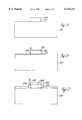
- a protecting layer 216is formed over the active regions 214.
- the protecting layer 216can be formed by, for example, depositing a dielectric material over the substrate 200 and optionally over the gate electrode 204 and spacer structure 210.
- the protecting layeris formed of a material, such as silicon dioxide, that allows the material of the second spacer 209 to be selectively etched.
- the protecting layer 216can be formed by a variety of techniques, including, for example, chemical vapor deposition, physical vapor deposition, or spin-on glass formation.
- a portion of the protecting layer 216can then be removed, particularly any portion of the protecting layer 216 over the gate electrode 204. This can be accomplished using techniques, such as, for example, chemical, mechanical, or chemical/mechanical polishing. A remaining portion of the protecting layer 216 is left substantially over the active regions 214, as shown in FIG. 2F.
- a portion of the gate electrode 204may be removed with the removal of a portion of the protecting layer 216 and/or in a second removal step. This can be accomplished using techniques, such as, for example, chemical, mechanical, or chemical/mechanical polishing. This process may also include removing additional portions of the protecting layer 216 and is useful for polishing the surface of the gate electrode 204.
- the second spacers 209are then removed to form openings 218 between the first spacers 207 and the protecting layer 216.
- the resultant structureis shown in FIG. 2F.
- the second spacers 209are typically removed using a selective etching technique.
- silicon nitride second spacers 209can be selectively etched with respect to silicon dioxide first spacers 207 and a silicon dioxide protecting layer 216.
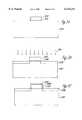
- a second dopant material 220is implanted through the openings 218 into the substrate 200 to form LDD regions 222 adjacent to the gate electrode 204 and the active regions 214, as shown in FIG. 2G.
- the second dopant material 220is the same conductivity type, although not necessarily the same material, as the first dopant material 212.
- the implant energies of the second dopant material 220can be in the range of, for example, 2 to 25 keV and the dopant dosage can be in the range of, for example, 1E13 (1 ⁇ 10 13 ) dopant atoms/cm 2 to 5E14 (5 ⁇ 10 14 ) dopant atoms/cm 2 , although higher or lower implant energies and dopant dosages may be used.
- the second dopant material in the LDD regionsmay optionally be annealed by heating after implantation.
- a third dopant material 224is implanted through the openings 218 to form first halo regions 226 that are deeper into the substrate 200 than the LDD regions 222 and adjacent to a lower portion of the active regions 214, as shown in FIG. 2H.
- the third dopant material 224is of a conductivity type different than that of the first and second dopant materials 212, 220 (i.e., if the first and second dopant materials are p-type than the third dopant material is n-type).
- the third dopant materialmay be implanted prior to the second dopant material.
- the implant energies of the third dopant material 216can be in the range of, for example, 5 to 40 keV and the dopant dosage can be in the range of, for example, 5E12 (5 ⁇ 10 12 ) dopant atoms/cm 2 to 1E14 (1 ⁇ 10 14 ) dopant atoms/cm 2 , although higher or lower implant energies and dopant dosages may be used.
- the protecting layer 216is sufficiently thick when the third dopant material is implanted to prevent or substantially reduce the implantation of the third dopant material into the active regions 214.
- a fourth dopant material 228is implanted through the openings 218 to form optional second halo regions 230 that are deeper in the substrate than the first halo regions 228, as shown in FIG. 2H.
- the optional fourth dopant material 228is of the same conductivity type as the third dopant material 224.
- the implant energies of the optional fourth dopant material 228are, for example, 5 to 15 keV larger than the implant energies of the third dopant material 224, and the dopant dosage can be in the range of, for example, 5E12 (5 ⁇ 10 12 ) dopant atoms/cm 2 to 1E14 (1 ⁇ 10 14 ) dopant atoms/cm 2 .
- the fourth dopant materialmay be implanted prior to the second and/or third dopant materials.
- the protecting layer 216is sufficiently thick when the fourth dopant material is implanted to prevent or substantially reduce the implantation of the fourth dopant material into the active regions 214. Additional processing steps, including, for example, reformation or enlargement of the spacer, silicidation, interconnect formation, and so forth may be performed to complete the ultimate device structure.
- active regions 214, halo regions 226, 230, and LDD regions 222are formed using a self-aligned process based, at least in part, on the provision of spacer structures 210.
- This self-aligned processcan result in the formation of semiconductor devices with greater uniformity than those formed by conventional techniques.
- the halo regionsare formed using a protecting layer that can prevent implantation of the halo region dopant material into the active regions. This can be advantageous as it may allow for shallower active regions and junctions. Many conventional techniques do not protect the active regions during implantation of dopant material to form the halo regions.
- FIGS. 3A through 3HAnother method is illustrated in FIGS. 3A through 3H.
- the process materials and conditionsare the same as the method illustrated in FIGS. 2A through 2I unless otherwise indicated.
- the methodincludes forming a gate insulation layer 304 and gate electrode 302 on a substrate 300, as shown in FIG. 3A.
- a first dopant material 306is implanted into the substrate to form LDD regions 308, as shown in FIG. 3B.
- the implant energies of the first dopant material 306can be in the range of, for example, 2 to 25 keV and the dopant dosage can be in the range of, for example, 1E13 (1 ⁇ 10 13 ) dopant atoms/cm 2 to 5E14 (5 ⁇ 10 14 ) dopant atoms/cm 2 , although higher or lower implant energies and dopant dosages may be used.
- the LDD regionsmay optionally be annealed by heating the substrate.
- a first spacer layer 310is formed over the substrate 300 and on a sidewall 305 of the gate electrode 304, as shown in FIG. 3C.
- the materials, thickness, and methods of forming the first spacer layer 310are the same as the first spacer layer 206 illustrated in FIG. 2B.
- the first spacer layeris formed prior to forming the LDD regions. The first dopant material may then be implanted into the substrate through the first spacer layer.
- a second spacer layer 312is formed over the first spacer layer 310, as shown in FIG. 3D.
- the second spacer layer 312can be formed using the same materials, thickness, and methods as the second spacer layer 208 illustrated in FIG. 2C. Portions of the first and second spacer layers 310, 312 can then be removed to leave first spacers 311 and second spacers 313 that form spacer structures 314 along the sidewalls 305 of the gate electrode 304.
- a second dopant material 316is implanted into the substrate 300 to form active regions 318 spaced apart from the gate electrode 304 by the spacer structures 314, as illustrated in FIG. 3E.
- the second dopant material 316is of the same conductivity type as the first dopant material 306, although not necessarily the same material.
- the implant energies of the second dopant material 316can be in the range of, for example, 5 to 30 keV and the dopant dosage can be in the range of, for example, 5E14 (5 ⁇ 10 14 ) dopant atoms/cm 2 to 5E15 (5 ⁇ 10 15 ) dopant atoms/cm 2 , although higher or lower implant energies and dopant dosages may be used.
- the active regionsmay optionally be annealed by heating the substrate.
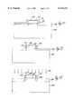
- a protective layer 320using the same materials, thicknesses, and processes as the protective layer 216 illustrated in FIG. 2F, is formed over the active regions 318, as shown in FIG. 3G.
- the second spacers 313are then removed to form openings 322 between the first spacers 311 and the protective layer 320, as also shown in FIG. 3G.
- a third dopant material 324is implanted into the substrate 300 through the opening 322 to form first halo regions 326 below the LDD regions 308 and adjacent to a lower portion of the active regions 318, as shown in FIG. 3H.
- the third dopant material 324is of a conductivity type different than that of the first and second dopant materials 306, 316 (i.e., if the first and second dopant materials are p-type than the third dopant material is n-type).
- the implant energies of the third dopant material 324can be in the range of, for example, 5 to 40 keV and the dopant dosage can be in the range of, for example, 5E12 (5 ⁇ 10 12 ) dopant atoms/cm 2 to 1E14 (1 ⁇ 10 14 ) dopant atoms/cm 2 , although higher or lower implant energies and dopant dosages may be used.
- a fourth dopant material(not shown) can be implanted in the substrate to form second halo regions (not shown) beneath the first halo regions.
- Yet another method of forming a semiconductor device with self-aligned active, halo, and LDD regionsincludes forming a spacer structure with a single layer of a material that can be selectively etched with respect to the protective layer. This modification can be made to either of the processes illustrated in FIGS. 2A through 2I or FIGS. 3A through 3H.
- This single layer of materialhas a thickness of, for example, 200 to 500 Angstroms.
- the spacer structureis removed either completely or partially (leaving only a thin (e.g., 50 Angstroms or less) portion of the spacer structure) after formation of the protecting layer to provide openings through which dopant material can be implanted to form LDD regions and/or halo regions.
- a halo regionmay be selectively formed on one side of the gate electrode by masking off the other side using, for example, a layer of dielectric material.
- CMOS devicescan be formed by a variety of techniques that utilize masking (e.g., masking with a dielectric or photoresist layer).
- PMOS and NMOS portions of the CMOS devicecan be formed independently (e.g., forming PMOS portions, masking the PMOS portions, and then forming the NMOS portions) or they can be formed simultaneously, except that one portion is masked during the implantation of a particular dopant material in the other portion (e.g., the PMOS portions are masked during implant of the first, second, third, or fourth dopant material in the NMOS portion and then the NMOS portion is masked during implant of the first, second, third, or fourth dopant material in the PMOS portion.)
- the present inventionis applicable to a number of different devices and systems that include a halo region to prevent or reduce punchthrough between active regions. Accordingly, the present invention should not be considered limited to the particular examples described above, but rather should be understood to cover all aspects of the invention as fairly set out in the attached claims. Various modifications, equivalent processes, as well as numerous communication devices to which the present invention may be applicable will be readily apparent to those of skill in the art upon review of the present specification. The claims are intended to cover such modifications and devices.
Landscapes
- Insulated Gate Type Field-Effect Transistor (AREA)
Abstract
Description
Claims (21)
Priority Applications (1)
| Application Number | Priority Date | Filing Date | Title |
|---|---|---|---|
| US09/195,336US6114211A (en) | 1998-11-18 | 1998-11-18 | Semiconductor device with vertical halo region and methods of manufacture |
Applications Claiming Priority (1)
| Application Number | Priority Date | Filing Date | Title |
|---|---|---|---|
| US09/195,336US6114211A (en) | 1998-11-18 | 1998-11-18 | Semiconductor device with vertical halo region and methods of manufacture |
Publications (1)
| Publication Number | Publication Date |
|---|---|
| US6114211Atrue US6114211A (en) | 2000-09-05 |
Family
ID=22721028
Family Applications (1)
| Application Number | Title | Priority Date | Filing Date |
|---|---|---|---|
| US09/195,336Expired - LifetimeUS6114211A (en) | 1998-11-18 | 1998-11-18 | Semiconductor device with vertical halo region and methods of manufacture |
Country Status (1)
| Country | Link |
|---|---|
| US (1) | US6114211A (en) |
Cited By (29)
| Publication number | Priority date | Publication date | Assignee | Title |
|---|---|---|---|---|
| US6297117B1 (en)* | 2001-02-12 | 2001-10-02 | Advanced Micro Devices, Inc. | Formation of confined halo regions in field effect transistor |
| US6335234B2 (en) | 1997-11-12 | 2002-01-01 | Micron Technology, Inc. | Methods of forming field effect transistors and related field effect transistor constructions |
| US6344405B1 (en)* | 2000-04-11 | 2002-02-05 | Philips Electronics North America Corp. | Transistors having optimized source-drain structures and methods for making the same |
| US20020093058A1 (en)* | 1998-09-03 | 2002-07-18 | Mcqueen Mark | Esd/eos protection structure for integrated circuit devices |
| US6472282B1 (en)* | 2000-08-15 | 2002-10-29 | Advanced Micro Devices, Inc. | Self-amorphized regions for transistors |
| US6503807B2 (en)* | 2001-03-13 | 2003-01-07 | United Microelectronics Corp. | MOS transistor with two empty side slots on its gate and its method of formation |
| US6509241B2 (en)* | 2000-12-12 | 2003-01-21 | International Business Machines Corporation | Process for fabricating an MOS device having highly-localized halo regions |
| US6555437B1 (en)* | 2001-04-27 | 2003-04-29 | Advanced Micro Devices, Inc. | Multiple halo implant in a MOSFET with raised source/drain structure |
| US6743689B1 (en)* | 2003-01-14 | 2004-06-01 | Advanced Micro Devices, Inc. | Method of fabrication SOI devices with accurately defined monocrystalline source/drain extensions |
| US20050139875A1 (en)* | 2003-12-27 | 2005-06-30 | Hak-Dong Kim | MOS transistors and methods of manufacturing the same |
| US6916716B1 (en) | 2003-10-24 | 2005-07-12 | Advanced Micro Devices, Inc. | Asymmetric halo implants |
| US7144782B1 (en) | 2004-07-02 | 2006-12-05 | Advanced Micro Devices, Inc. | Simplified masking for asymmetric halo |
| US7170084B1 (en)* | 2002-09-30 | 2007-01-30 | Advanced Micro Devices, Inc. | Strained silicon MOSFET having improved source/drain extension dopant diffusion resistance and method for its fabrication |
| US7176095B1 (en) | 2004-03-01 | 2007-02-13 | Advanced Micro Devices, Inc. | Bi-modal halo implantation |
| US7192836B1 (en)* | 1999-11-29 | 2007-03-20 | Advanced Micro Devices, Inc. | Method and system for providing halo implant to a semiconductor device with minimal impact to the junction capacitance |
| US20100065924A1 (en)* | 2008-09-16 | 2010-03-18 | Jing-Cheng Lin | Ultra-Shallow Junctions using Atomic-Layer Doping |
| US20100117160A1 (en)* | 2008-11-07 | 2010-05-13 | Seagate Technology Llc | Polarity dependent switch for resistive sense memory |
| US7936580B2 (en) | 2008-10-20 | 2011-05-03 | Seagate Technology Llc | MRAM diode array and access method |
| US7936583B2 (en) | 2008-10-30 | 2011-05-03 | Seagate Technology Llc | Variable resistive memory punchthrough access method |
| US7974119B2 (en) | 2008-07-10 | 2011-07-05 | Seagate Technology Llc | Transmission gate-based spin-transfer torque memory unit |
| US8158964B2 (en) | 2009-07-13 | 2012-04-17 | Seagate Technology Llc | Schottky diode switch and memory units containing the same |
| US8159856B2 (en) | 2009-07-07 | 2012-04-17 | Seagate Technology Llc | Bipolar select device for resistive sense memory |
| US20120098072A1 (en)* | 2010-10-20 | 2012-04-26 | Seung-Uk Han | Semiconductor Devices Having Lightly Doped Channel Impurity Regions |
| US8178864B2 (en) | 2008-11-18 | 2012-05-15 | Seagate Technology Llc | Asymmetric barrier diode |
| US8203869B2 (en) | 2008-12-02 | 2012-06-19 | Seagate Technology Llc | Bit line charge accumulation sensing for resistive changing memory |
| US8648426B2 (en) | 2010-12-17 | 2014-02-11 | Seagate Technology Llc | Tunneling transistors |
| US9030867B2 (en) | 2008-10-20 | 2015-05-12 | Seagate Technology Llc | Bipolar CMOS select device for resistive sense memory |
| CN106206719A (en)* | 2015-05-05 | 2016-12-07 | 中芯国际集成电路制造(上海)有限公司 | Mos transistor and forming method thereof |
| US10475901B1 (en)* | 2018-04-19 | 2019-11-12 | Globalfoundries Inc. | Cap removal for gate electrode structures with reduced complexity |
Citations (5)
| Publication number | Priority date | Publication date | Assignee | Title |
|---|---|---|---|---|
| US5578509A (en)* | 1993-04-23 | 1996-11-26 | Mitsubishi Denki Kabushiki Kaisha | Method of making a field effect transistor |
| US5595919A (en)* | 1996-02-20 | 1997-01-21 | Chartered Semiconductor Manufacturing Pte Ltd. | Method of making self-aligned halo process for reducing junction capacitance |
| US5736446A (en)* | 1997-05-21 | 1998-04-07 | Powerchip Semiconductor Corp. | Method of fabricating a MOS device having a gate-side air-gap structure |
| US5830788A (en)* | 1996-06-21 | 1998-11-03 | Matsushita Electric Industrial Co., Ltd. | Method for forming complementary MOS device having asymmetric region in channel region |
| US5885886A (en)* | 1996-12-26 | 1999-03-23 | Lg Semicon Co., Ltd. | Method for manufacturing semiconductor device |
- 1998
- 1998-11-18USUS09/195,336patent/US6114211A/ennot_activeExpired - Lifetime
Patent Citations (5)
| Publication number | Priority date | Publication date | Assignee | Title |
|---|---|---|---|---|
| US5578509A (en)* | 1993-04-23 | 1996-11-26 | Mitsubishi Denki Kabushiki Kaisha | Method of making a field effect transistor |
| US5595919A (en)* | 1996-02-20 | 1997-01-21 | Chartered Semiconductor Manufacturing Pte Ltd. | Method of making self-aligned halo process for reducing junction capacitance |
| US5830788A (en)* | 1996-06-21 | 1998-11-03 | Matsushita Electric Industrial Co., Ltd. | Method for forming complementary MOS device having asymmetric region in channel region |
| US5885886A (en)* | 1996-12-26 | 1999-03-23 | Lg Semicon Co., Ltd. | Method for manufacturing semiconductor device |
| US5736446A (en)* | 1997-05-21 | 1998-04-07 | Powerchip Semiconductor Corp. | Method of fabricating a MOS device having a gate-side air-gap structure |
Non-Patent Citations (10)
| Title |
|---|
| A 0.8UM CMOS Technology for High Performance ASIC Memory and Channelless Gate Array, IEEE, pp. 1 4, 1988.* |
| A 0.8UM CMOS Technology for High Performance ASIC Memory and Channelless Gate Array, IEEE, pp. 1-4, 1988. |
| Wolf, Silicon Processing for the VLSI Era , Lattice Press, vol. 2: Process Integration, pp. 354 363 (1990).* |
| Wolf, Silicon Processing for the VLSI Era , Lattice Press, vol. 3, The Submicron MOSFET, pp. 232 240, (1995).* |
| Wolf, Silicon Processing for the VLSI Era , Lattice Press, vol. 3, The Submicron MOSFET, pp. 309 311, (1995).* |
| Wolf, Silicon Processing for the VLSI Era , Lattice Press, vol. 3, The Submicron MOSFET, pp. 621 622, (1995).* |
| Wolf, Silicon Processing for the VLSI Era, Lattice Press, vol. 2: Process Integration, pp. 354-363 (1990). |
| Wolf, Silicon Processing for the VLSI Era, Lattice Press, vol. 3, The Submicron MOSFET, pp. 232-240, (1995). |
| Wolf, Silicon Processing for the VLSI Era, Lattice Press, vol. 3, The Submicron MOSFET, pp. 309-311, (1995). |
| Wolf, Silicon Processing for the VLSI Era, Lattice Press, vol. 3, The Submicron MOSFET, pp. 621-622, (1995). |
Cited By (62)
| Publication number | Priority date | Publication date | Assignee | Title |
|---|---|---|---|---|
| US6406957B1 (en) | 1997-11-12 | 2002-06-18 | Micron Technology, Inc. | Methods of forming field effect transistors and related field effect transistor constructions |
| US6335246B1 (en) | 1997-11-12 | 2002-01-01 | Micron Technology, Inc. | Methods of forming field effect transistors and related field effect transistor constructions |
| US6344382B1 (en) | 1997-11-12 | 2002-02-05 | Micron Technology, Inc. | Methods of forming field effect transistors and related field effect transistor constructions |
| US6400002B1 (en) | 1997-11-12 | 2002-06-04 | Micron Technology, Inc. | Methods of forming field effect transistors and related field effect transistor constructions |
| US6335234B2 (en) | 1997-11-12 | 2002-01-01 | Micron Technology, Inc. | Methods of forming field effect transistors and related field effect transistor constructions |
| US6673663B2 (en) | 1997-11-12 | 2004-01-06 | Micron Technology, Inc. | Methods of forming field effect transistors and related field effect transistor constructions |
| US6472260B2 (en) | 1997-11-12 | 2002-10-29 | Micron Technology, Inc. | Methods of forming field effect transistors and related field effect transistor constructions |
| US6413823B1 (en) | 1997-11-12 | 2002-07-02 | Micron Technology, Inc. | Methods of forming field effect transistors |
| US6475852B2 (en) | 1997-11-12 | 2002-11-05 | Micron Technology, Inc. | Method of forming field effect transistors and related field effect transistor constructions |
| US6482691B2 (en)* | 1997-11-12 | 2002-11-19 | Micron Technology, Inc. | Seismic imaging using omni-azimuth seismic energy sources and directional sensing |
| US6844600B2 (en) | 1998-09-03 | 2005-01-18 | Micron Technology, Inc. | ESD/EOS protection structure for integrated circuit devices |
| US6835650B1 (en)* | 1998-09-03 | 2004-12-28 | Micron Technology, Inc. | ESD/EOS protection structure for integrated circuit devices and methods of fabricating the same |
| US20020093058A1 (en)* | 1998-09-03 | 2002-07-18 | Mcqueen Mark | Esd/eos protection structure for integrated circuit devices |
| US7192836B1 (en)* | 1999-11-29 | 2007-03-20 | Advanced Micro Devices, Inc. | Method and system for providing halo implant to a semiconductor device with minimal impact to the junction capacitance |
| US6344405B1 (en)* | 2000-04-11 | 2002-02-05 | Philips Electronics North America Corp. | Transistors having optimized source-drain structures and methods for making the same |
| US6472282B1 (en)* | 2000-08-15 | 2002-10-29 | Advanced Micro Devices, Inc. | Self-amorphized regions for transistors |
| US6509241B2 (en)* | 2000-12-12 | 2003-01-21 | International Business Machines Corporation | Process for fabricating an MOS device having highly-localized halo regions |
| US6297117B1 (en)* | 2001-02-12 | 2001-10-02 | Advanced Micro Devices, Inc. | Formation of confined halo regions in field effect transistor |
| US6503807B2 (en)* | 2001-03-13 | 2003-01-07 | United Microelectronics Corp. | MOS transistor with two empty side slots on its gate and its method of formation |
| US6555437B1 (en)* | 2001-04-27 | 2003-04-29 | Advanced Micro Devices, Inc. | Multiple halo implant in a MOSFET with raised source/drain structure |
| US7170084B1 (en)* | 2002-09-30 | 2007-01-30 | Advanced Micro Devices, Inc. | Strained silicon MOSFET having improved source/drain extension dopant diffusion resistance and method for its fabrication |
| US6743689B1 (en)* | 2003-01-14 | 2004-06-01 | Advanced Micro Devices, Inc. | Method of fabrication SOI devices with accurately defined monocrystalline source/drain extensions |
| US6916716B1 (en) | 2003-10-24 | 2005-07-12 | Advanced Micro Devices, Inc. | Asymmetric halo implants |
| US20050139875A1 (en)* | 2003-12-27 | 2005-06-30 | Hak-Dong Kim | MOS transistors and methods of manufacturing the same |
| US7223663B2 (en)* | 2003-12-27 | 2007-05-29 | Dongbu Electronics Co., Ltd. | MOS transistors and methods of manufacturing the same |
| US20070194376A1 (en)* | 2003-12-27 | 2007-08-23 | Dongbu Electronics Co., Ltd. | MOS transistors and methods of manufacturing the same |
| US7176095B1 (en) | 2004-03-01 | 2007-02-13 | Advanced Micro Devices, Inc. | Bi-modal halo implantation |
| US7144782B1 (en) | 2004-07-02 | 2006-12-05 | Advanced Micro Devices, Inc. | Simplified masking for asymmetric halo |
| US7974119B2 (en) | 2008-07-10 | 2011-07-05 | Seagate Technology Llc | Transmission gate-based spin-transfer torque memory unit |
| US8199563B2 (en) | 2008-07-10 | 2012-06-12 | Seagate Technology Llc | Transmission gate-based spin-transfer torque memory unit |
| US8416615B2 (en) | 2008-07-10 | 2013-04-09 | Seagate Technology Llc | Transmission gate-based spin-transfer torque memory unit |
| US20100065924A1 (en)* | 2008-09-16 | 2010-03-18 | Jing-Cheng Lin | Ultra-Shallow Junctions using Atomic-Layer Doping |
| US8361895B2 (en)* | 2008-09-16 | 2013-01-29 | Taiwan Semiconductor Manufacturing Company, Ltd. | Ultra-shallow junctions using atomic-layer doping |
| US8514605B2 (en) | 2008-10-20 | 2013-08-20 | Seagate Technology Llc | MRAM diode array and access method |
| US7936580B2 (en) | 2008-10-20 | 2011-05-03 | Seagate Technology Llc | MRAM diode array and access method |
| US9030867B2 (en) | 2008-10-20 | 2015-05-12 | Seagate Technology Llc | Bipolar CMOS select device for resistive sense memory |
| US8289746B2 (en) | 2008-10-20 | 2012-10-16 | Seagate Technology Llc | MRAM diode array and access method |
| US7961497B2 (en) | 2008-10-30 | 2011-06-14 | Seagate Technology Llc | Variable resistive memory punchthrough access method |
| US7936583B2 (en) | 2008-10-30 | 2011-05-03 | Seagate Technology Llc | Variable resistive memory punchthrough access method |
| US8508981B2 (en) | 2008-10-30 | 2013-08-13 | Seagate Technology Llc | Apparatus for variable resistive memory punchthrough access method |
| US8098510B2 (en) | 2008-10-30 | 2012-01-17 | Seagate Technology Llc | Variable resistive memory punchthrough access method |
| US8199558B2 (en) | 2008-10-30 | 2012-06-12 | Seagate Technology Llc | Apparatus for variable resistive memory punchthrough access method |
| US20100117160A1 (en)* | 2008-11-07 | 2010-05-13 | Seagate Technology Llc | Polarity dependent switch for resistive sense memory |
| US7825478B2 (en) | 2008-11-07 | 2010-11-02 | Seagate Technology Llc | Polarity dependent switch for resistive sense memory |
| US8508980B2 (en) | 2008-11-07 | 2013-08-13 | Seagate Technology Llc | Polarity dependent switch for resistive sense memory |
| US8072014B2 (en) | 2008-11-07 | 2011-12-06 | Seagate Technology Llc | Polarity dependent switch for resistive sense memory |
| US7935619B2 (en) | 2008-11-07 | 2011-05-03 | Seagate Technology Llc | Polarity dependent switch for resistive sense memory |
| US8178864B2 (en) | 2008-11-18 | 2012-05-15 | Seagate Technology Llc | Asymmetric barrier diode |
| US8203869B2 (en) | 2008-12-02 | 2012-06-19 | Seagate Technology Llc | Bit line charge accumulation sensing for resistive changing memory |
| US8638597B2 (en) | 2008-12-02 | 2014-01-28 | Seagate Technology Llc | Bit line charge accumulation sensing for resistive changing memory |
| US8159856B2 (en) | 2009-07-07 | 2012-04-17 | Seagate Technology Llc | Bipolar select device for resistive sense memory |
| US8514608B2 (en) | 2009-07-07 | 2013-08-20 | Seagate Technology Llc | Bipolar select device for resistive sense memory |
| US8198181B1 (en) | 2009-07-13 | 2012-06-12 | Seagate Technology Llc | Schottky diode switch and memory units containing the same |
| US8288749B2 (en) | 2009-07-13 | 2012-10-16 | Seagate Technology Llc | Schottky diode switch and memory units containing the same |
| US8158964B2 (en) | 2009-07-13 | 2012-04-17 | Seagate Technology Llc | Schottky diode switch and memory units containing the same |
| US20120098072A1 (en)* | 2010-10-20 | 2012-04-26 | Seung-Uk Han | Semiconductor Devices Having Lightly Doped Channel Impurity Regions |
| US8742473B2 (en)* | 2010-10-20 | 2014-06-03 | Samsung Electronics Co., Ltd. | Semiconductor devices having lightly doped channel impurity regions |
| US8648426B2 (en) | 2010-12-17 | 2014-02-11 | Seagate Technology Llc | Tunneling transistors |
| CN106206719A (en)* | 2015-05-05 | 2016-12-07 | 中芯国际集成电路制造(上海)有限公司 | Mos transistor and forming method thereof |
| CN106206719B (en)* | 2015-05-05 | 2019-08-27 | 中芯国际集成电路制造(上海)有限公司 | MOS transistor and forming method thereof |
| US10475901B1 (en)* | 2018-04-19 | 2019-11-12 | Globalfoundries Inc. | Cap removal for gate electrode structures with reduced complexity |
| US11195935B2 (en) | 2018-04-19 | 2021-12-07 | Globalfoundries U.S. Inc. | Semiconductor device with novel spacer structures having novel configurations |
Similar Documents
| Publication | Publication Date | Title |
|---|---|---|
| US6114211A (en) | Semiconductor device with vertical halo region and methods of manufacture | |
| US6300205B1 (en) | Method of making a semiconductor device with self-aligned active, lightly-doped drain, and halo regions | |
| US5677224A (en) | Method of making asymmetrical N-channel and P-channel devices | |
| US5937301A (en) | Method of making a semiconductor device having sidewall spacers with improved profiles | |
| US6316302B1 (en) | Isotropically etching sidewall spacers to be used for both an NMOS source/drain implant and a PMOS LDD implant | |
| US5930642A (en) | Transistor with buried insulative layer beneath the channel region | |
| US5933721A (en) | Method for fabricating differential threshold voltage transistor pair | |
| US7544573B2 (en) | Semiconductor device including MOS field effect transistor having offset spacers or gate sidewall films on either side of gate electrode and method of manufacturing the same | |
| US6096591A (en) | Method of making an IGFET and a protected resistor with reduced processing steps | |
| US6013546A (en) | Semiconductor device having a PMOS device with a source/drain region formed using a heavy atom p-type implant and method of manufacture thereof | |
| US6146934A (en) | Semiconductor device with asymmetric PMOS source/drain implant and method of manufacture thereof | |
| US6525391B1 (en) | Nickel silicide process using starved silicon diffusion barrier | |
| EP1280191A2 (en) | A method to form elevated source/drain regions using polysilicon spacers | |
| US6207482B1 (en) | Integration method for deep sub-micron dual gate transistor design | |
| US6027964A (en) | Method of making an IGFET with a selectively doped gate in combination with a protected resistor | |
| US6117739A (en) | Semiconductor device with layered doped regions and methods of manufacture | |
| US5946581A (en) | Method of manufacturing a semiconductor device by doping an active region after formation of a relatively thick oxide layer | |
| US6008100A (en) | Metal-oxide semiconductor field effect transistor device fabrication process | |
| US6162694A (en) | Method of forming a metal gate electrode using replaced polysilicon structure | |
| CN108231767B (en) | Device structure with multiple nitride layers | |
| US5930632A (en) | Process of fabricating a semiconductor device having cobalt niobate gate electrode structure | |
| US6724051B1 (en) | Nickel silicide process using non-reactive spacer | |
| US5976925A (en) | Process of fabricating a semiconductor devise having asymmetrically-doped active region and gate electrode | |
| US6051471A (en) | Method for making asymmetrical N-channel and symmetrical P-channel devices | |
| US6074906A (en) | Complementary metal-oxide semiconductor device having source/drain regions formed using multiple spacers |
Legal Events
| Date | Code | Title | Description |
|---|---|---|---|
| AS | Assignment | Owner name:ADVANCED MICRO DEVICES, TEXAS Free format text:ASSIGNMENT OF ASSIGNORS INTEREST;ASSIGNORS:FULFORD, H. JIM;CHEEK, JON;WRISTERS, DERICK J.;AND OTHERS;REEL/FRAME:009597/0727 Effective date:19981116 | |
| STCF | Information on status: patent grant | Free format text:PATENTED CASE | |
| FPAY | Fee payment | Year of fee payment:4 | |
| FPAY | Fee payment | Year of fee payment:8 | |
| AS | Assignment | Owner name:GLOBALFOUNDRIES INC., CAYMAN ISLANDS Free format text:AFFIRMATION OF PATENT ASSIGNMENT;ASSIGNOR:ADVANCED MICRO DEVICES, INC.;REEL/FRAME:023119/0083 Effective date:20090630 | |
| FPAY | Fee payment | Year of fee payment:12 | |
| AS | Assignment | Owner name:WILMINGTON TRUST, NATIONAL ASSOCIATION, DELAWARE Free format text:SECURITY AGREEMENT;ASSIGNOR:GLOBALFOUNDRIES INC.;REEL/FRAME:049490/0001 Effective date:20181127 | |
| AS | Assignment | Owner name:GLOBALFOUNDRIES INC., CAYMAN ISLANDS Free format text:RELEASE BY SECURED PARTY;ASSIGNOR:WILMINGTON TRUST, NATIONAL ASSOCIATION;REEL/FRAME:054636/0001 Effective date:20201117 | |
| AS | Assignment | Owner name:GLOBALFOUNDRIES U.S. INC., NEW YORK Free format text:RELEASE BY SECURED PARTY;ASSIGNOR:WILMINGTON TRUST, NATIONAL ASSOCIATION;REEL/FRAME:056987/0001 Effective date:20201117 |