US6114206A - Multiple threshold voltage transistor implemented by a damascene process - Google Patents
Multiple threshold voltage transistor implemented by a damascene processDownload PDFInfo
- Publication number
- US6114206A US6114206AUS09/187,171US18717198AUS6114206AUS 6114206 AUS6114206 AUS 6114206AUS 18717198 AUS18717198 AUS 18717198AUS 6114206 AUS6114206 AUS 6114206A
- Authority
- US
- United States
- Prior art keywords
- gate
- germanium
- layer
- transistors
- gate structures
- Prior art date
- Legal status (The legal status is an assumption and is not a legal conclusion. Google has not performed a legal analysis and makes no representation as to the accuracy of the status listed.)
- Expired - Lifetime
Links
- 238000000034methodMethods0.000titleclaimsabstractdescription58
- 230000008569processEffects0.000titleclaimsabstractdescription34
- 239000000463materialSubstances0.000claimsabstractdescription76
- 229910052732germaniumInorganic materials0.000claimsabstractdescription69
- GNPVGFCGXDBREM-UHFFFAOYSA-Ngermanium atomChemical compound[Ge]GNPVGFCGXDBREM-UHFFFAOYSA-N0.000claimsabstractdescription63
- 229910021420polycrystalline siliconInorganic materials0.000claimsabstractdescription47
- 229920005591polysiliconPolymers0.000claimsabstractdescription47
- 239000004020conductorSubstances0.000claimsdescription42
- 239000002019doping agentSubstances0.000claimsdescription34
- 239000004065semiconductorSubstances0.000claimsdescription31
- 238000004519manufacturing processMethods0.000claimsdescription15
- 239000000758substrateSubstances0.000claimsdescription15
- XUIMIQQOPSSXEZ-UHFFFAOYSA-NSiliconChemical compound[Si]XUIMIQQOPSSXEZ-UHFFFAOYSA-N0.000claimsdescription12
- 229910052710siliconInorganic materials0.000claimsdescription12
- 239000010703siliconSubstances0.000claimsdescription12
- 230000004888barrier functionEffects0.000claimsdescription10
- 238000000151depositionMethods0.000claimsdescription9
- 229920002120photoresistant polymerPolymers0.000claimsdescription9
- 125000006850spacer groupChemical group0.000claimsdescription8
- -1germanium ionsChemical class0.000claimsdescription7
- ZOXJGFHDIHLPTG-UHFFFAOYSA-NBoronChemical compound[B]ZOXJGFHDIHLPTG-UHFFFAOYSA-N0.000claimsdescription6
- 229910052796boronInorganic materials0.000claimsdescription6
- 238000001039wet etchingMethods0.000claimsdescription5
- 150000002500ionsChemical class0.000claimsdescription4
- 230000005669field effectEffects0.000claimsdescription3
- 238000005530etchingMethods0.000claimsdescription2
- 238000005498polishingMethods0.000claims1
- 239000010408filmSubstances0.000description38
- 239000007943implantSubstances0.000description28
- 238000005224laser annealingMethods0.000description10
- VYPSYNLAJGMNEJ-UHFFFAOYSA-NSilicium dioxideChemical compoundO=[Si]=OVYPSYNLAJGMNEJ-UHFFFAOYSA-N0.000description8
- 229910021417amorphous siliconInorganic materials0.000description6
- 238000005229chemical vapour depositionMethods0.000description5
- 230000008021depositionEffects0.000description4
- 238000004518low pressure chemical vapour depositionMethods0.000description4
- 238000000137annealingMethods0.000description3
- 230000000694effectsEffects0.000description3
- 238000002513implantationMethods0.000description3
- 238000005468ion implantationMethods0.000description3
- 239000000203mixtureSubstances0.000description3
- 150000004767nitridesChemical class0.000description3
- 235000012239silicon dioxideNutrition0.000description3
- 239000000377silicon dioxideSubstances0.000description3
- 230000003213activating effectEffects0.000description2
- 230000015572biosynthetic processEffects0.000description2
- 230000015556catabolic processEffects0.000description2
- 238000006731degradation reactionMethods0.000description2
- OKZIUSOJQLYFSE-UHFFFAOYSA-NdifluoroboronChemical compoundF[B]FOKZIUSOJQLYFSE-UHFFFAOYSA-N0.000description2
- 238000010438heat treatmentMethods0.000description2
- 238000002955isolationMethods0.000description2
- 230000008018meltingEffects0.000description2
- 238000002844meltingMethods0.000description2
- 229910044991metal oxideInorganic materials0.000description2
- 150000004706metal oxidesChemical class0.000description2
- 229910052814silicon oxideInorganic materials0.000description2
- 239000007787solidSubstances0.000description2
- OAICVXFJPJFONN-UHFFFAOYSA-NPhosphorusChemical compound[P]OAICVXFJPJFONN-UHFFFAOYSA-N0.000description1
- 229910052581Si3N4Inorganic materials0.000description1
- 230000002411adverseEffects0.000description1
- 238000005280amorphizationMethods0.000description1
- 229910052785arsenicInorganic materials0.000description1
- RQNWIZPPADIBDY-UHFFFAOYSA-Narsenic atomChemical compound[As]RQNWIZPPADIBDY-UHFFFAOYSA-N0.000description1
- 230000008859changeEffects0.000description1
- 239000002800charge carrierSubstances0.000description1
- 230000000295complement effectEffects0.000description1
- 239000013078crystalSubstances0.000description1
- 230000003247decreasing effectEffects0.000description1
- 230000001419dependent effectEffects0.000description1
- 238000009826distributionMethods0.000description1
- 238000001312dry etchingMethods0.000description1
- 239000012535impuritySubstances0.000description1
- 238000011065in-situ storageMethods0.000description1
- 239000011810insulating materialSubstances0.000description1
- 230000004048modificationEffects0.000description1
- 238000012986modificationMethods0.000description1
- 238000012856packingMethods0.000description1
- 229910052698phosphorusInorganic materials0.000description1
- 239000011574phosphorusSubstances0.000description1
- HQVNEWCFYHHQES-UHFFFAOYSA-Nsilicon nitrideChemical compoundN12[Si]34N5[Si]62N3[Si]51N64HQVNEWCFYHHQES-UHFFFAOYSA-N0.000description1
- 238000003860storageMethods0.000description1
- 239000010409thin filmSubstances0.000description1
Images


Classifications
- H—ELECTRICITY
- H10—SEMICONDUCTOR DEVICES; ELECTRIC SOLID-STATE DEVICES NOT OTHERWISE PROVIDED FOR
- H10D—INORGANIC ELECTRIC SEMICONDUCTOR DEVICES
- H10D64/00—Electrodes of devices having potential barriers
- H10D64/01—Manufacture or treatment
- H10D64/017—Manufacture or treatment using dummy gates in processes wherein at least parts of the final gates are self-aligned to the dummy gates, i.e. replacement gate processes
- H—ELECTRICITY
- H10—SEMICONDUCTOR DEVICES; ELECTRIC SOLID-STATE DEVICES NOT OTHERWISE PROVIDED FOR
- H10D—INORGANIC ELECTRIC SEMICONDUCTOR DEVICES
- H10D84/00—Integrated devices formed in or on semiconductor substrates that comprise only semiconducting layers, e.g. on Si wafers or on GaAs-on-Si wafers
- H10D84/01—Manufacture or treatment
- H10D84/0123—Integrating together multiple components covered by H10D12/00 or H10D30/00, e.g. integrating multiple IGBTs
- H10D84/0126—Integrating together multiple components covered by H10D12/00 or H10D30/00, e.g. integrating multiple IGBTs the components including insulated gates, e.g. IGFETs
- H10D84/0135—Manufacturing their gate conductors
- H10D84/014—Manufacturing their gate conductors the gate conductors having different materials or different implants
- H—ELECTRICITY
- H10—SEMICONDUCTOR DEVICES; ELECTRIC SOLID-STATE DEVICES NOT OTHERWISE PROVIDED FOR
- H10D—INORGANIC ELECTRIC SEMICONDUCTOR DEVICES
- H10D84/00—Integrated devices formed in or on semiconductor substrates that comprise only semiconducting layers, e.g. on Si wafers or on GaAs-on-Si wafers
- H10D84/01—Manufacture or treatment
- H10D84/02—Manufacture or treatment characterised by using material-based technologies
- H10D84/03—Manufacture or treatment characterised by using material-based technologies using Group IV technology, e.g. silicon technology or silicon-carbide [SiC] technology
- H10D84/038—Manufacture or treatment characterised by using material-based technologies using Group IV technology, e.g. silicon technology or silicon-carbide [SiC] technology using silicon technology, e.g. SiGe
Definitions
- the present inventionrelates generally to an integrated circuit (IC) and the fabrication of an integrated circuit. More particularly, the present invention relates to an integrated circuit having transistors with multiple threshold voltage values.
- Ultra-large-scale integrated (ULSI) circuitsgenerally include a multitude of transistors, such as, more than one million transistors and even several million transistors, that cooperate to perform various functions for an electronic component. Some transistors on the integrated circuit (IC) or chip are part of circuits which perform different operations than other circuits.
- ICintegrated circuit
- transistorsperform functions for circuits in the critical signal path of the IC, where speed is crucial to the proper operation of the IC.
- other transistorsperform functions for circuits in the non-critical signal path of the IC, where speed is not as important.
- Transistors in the non-critical signal pathare preferably designed to consume less power than transistors in the critical signal path.
- other transistorsmay perform functions for a signal path having a criticality somewhere between the critical signal path and the non-critical signal path and accordingly have different speed and power consumption requirements.
- transistors which have higher threshold voltagesconsume less power than transistors which have low threshold voltages due to smaller off-state current leakage.
- Threshold voltagerefers to the minimum gate voltage necessary for the onset of current flow between the source and the drain of a transistor.
- Transistors which have lower threshold voltagesare faster (e.g., have quicker switching speeds) than transistors which have higher threshold voltages.
- transistorssuch as, metal oxide semiconductor field effect transistors (MOSFETs)
- MOSFETsmetal oxide semiconductor field effect transistors
- MOSFETsmetal oxide semiconductor field effect transistors
- the non-critical signal pathe.g. storage devices
- ULSI circuitsare generally manufactured in accordance with complementary metal oxide semiconductor (CMOS) technology and design criteria which utilize N-channel MOSFETs and P-channel MOSFETs.
- CMOScomplementary metal oxide semiconductor
- the N-channel and P-channel MOSFETsgenerally include a polysilicon gate structure disposed between a drain and a source.
- the polysilicon gate structurecontrols charge carriers in a channel region to turn the transistor on and off.
- Utilizing channel implants to adjust the threshold voltages of transistorscan be problematic because transistor short channel performance is very susceptible to process variations.
- short channel performanceis extremely sensitive to channel implants or additional doping steps. Accordingly, the modification of the channel with implants can result in significantly different short channel performance between transistors, which adversely affects the predictability of the design and operability of the IC. This characteristic is particularly problematic as transistors become smaller and packing densities increase. Additionally, providing channel implants adds additional steps to the fabrication process and makes the IC more difficult to manufacture.
- the present inventionrelates to a method of manufacturing an integrated circuit.
- the methodincludes providing gate structures which include a dummy material above a gate dielectric, stripping the dummy material, proving a doped semiconductor material in a cavity left by the dummy material, and implanting a second semiconductor material in the doped semiconductor material of at least one of the gate structures.
- the second semiconductor materialaffect a work function associated with the at least one gate structure.
- Each of the gate structuresare disposed between a source region and a drain region in a semiconductor substrate.
- the present inventionstill further relates to a method of manufacturing an ultra-large scale integrated circuit including field effect transistors.
- Each transistorhas a source, a drain and a gate structure disposed between the source and the drain.
- the gate structureincludes a first gate material disposed over a gate oxide.
- the methodincludes steps of depositing a barrier layer over the top surface of the semiconductor substrate and over the gate structures, depositing an insulative material over the top surface of the semiconductor substrate and over the gate structures, removing a portion of the insulative layer and the barrier layer to expose the first gate material, removing the first gate material from the gate structures, providing a second gate material to the gate structures and implanting semiconductor ions in the second gate material of selected gate structures.
- the present inventionstill further relates to a damascene gate process of forming a heavily doped polysilicon gate conductor implanted with germanium.
- the processincludes steps of forming a plurality of at least a portion of the gate structures on a top surface of a silicon substrate, stripping the gate conductor from the gate structure, thereby leaving a cavity in the gate structure, providing a heavily doped polysilicon conductor in the cavity, and implanting the heavily doped polysilicon conductor with germanium ions.
- FIG. 1is a cross-sectional view of a portion of an integrated circuit in accordance with an exemplary embodiment of the present invention
- FIG. 2is a cross-sectional view of the portion of the integrated circuit illustrated in FIG. 1, showing a germanium ion implant step;
- FIG. 3is a cross-sectional view of the portion of the integrated circuit illustrated in FIG. 1, showing a photoresist removal step;
- FIG. 4is a cross-sectional view of the portion of the integrated circuit illustrated in FIG. 1, showing a gate stack formation step;
- FIG. 5is a cross-sectional view of a portion of another integrated circuit in accordance with another exemplary embodiment of the present invention.
- FIG. 6is a cross-sectional view of a polysilicon/germanium film in accordance with yet another exemplary embodiment of the present invention, the germanium film can be utilized in the portion of the integrated circuit illustrated in FIG. 1;
- FIG. 7is a cross-sectional view of the polysilicon/germanium film illustrated in FIG. 6, showing an amorphous silicon deposition step;
- FIG. 8is a cross-sectional view of the polysilicon/germanium film illustrated in FIG. 6, showing an amorphous germanium deposition step film;
- FIG. 9is a cross-sectional view of the polysilicon/germanium film illustrated in FIG. 6, showing a dopant implant step
- FIG. 10is a cross-sectional view of a polysilicon film in accordance with still another exemplary embodiment of the present invention, the polysilicon film can be utilized in the portion of the integrated circuit illustrated in FIG. 1;
- FIG. 11is a cross-sectional view of the polysilicon film illustrated in FIG. 10, showing an amorphous silicon deposition step;
- FIG. 12is a cross-sectional view of the polysilicon film illustrated in FIG. 1, showing a dopant implant step
- FIG. 13is a cross-sectional view of a portion of yet another integrated circuit in accordance with still yet another exemplary embodiment of the present invention.
- FIG. 14is a cross-sectional view of the portion of the integrated circuit illustrated in FIG. 13, showing dummy gate structures
- FIG. 15is a cross-sectional view of the portion of the integrated circuit illustrated in FIG. 13, showing a chemical-mechanical polish (CMP) step;
- CMPchemical-mechanical polish
- FIG. 16is a cross-sectional view of the portion of the integrated circuit illustrated in FIG. 13, showing a wet-etching step
- FIG. 17is a cross-sectional view of the portion of the integrated circuit illustrated in FIG. 13, showing a refill step
- FIG. 18is a cross-sectional view of the portion of the integrated circuit illustrated in FIG. 13, showing a germanium implantation step.
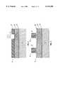
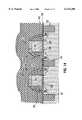
- a portion 10 of an integrated circuit (IC) or chipincludes a transistor 12 and a second transistor 14.
- Portion 10is preferably part of an ultra-large-scale integrated (ULSI) circuit having 1,000,000 or more transistors.
- ULSIultra-large-scale integrated
- Portion 10is manufactured as part of the IC on a semiconductor wafer, such as, a silicon wafer.
- Transistors 12 and 14are disposed on a substrate 16 that is preferably silicon.
- Transistor 12includes a gate stack 18, and transistor 14 includes a gate stack 20.
- Each of gate stack 18 and gate stack 20includes sidewall spacers 22, a gate dielectric 24, and a protection layer 26.
- Protection layer 26is preferably silicon oxynitride (SiON) or silicon nitride material.
- Spacers 22 and dielectric 24can be silicon dioxide or other insulating material. Spacers 22 are deposited as a dioxide layer by chemical vapor deposition (CVD), which is selectively etched. Dielectric 24 is thermally grown. Alternatively, spacers 22 can be a nitride material or other insulative.
- Transistors 12 and 14also both include a drain 30, a source 32, and a channel 34.
- Channel 34 of transistor 18has almost identical characteristics to channel 34 of transistor 20.
- Transistors 18 and 20are made with the same identical channel implant to avoid short channel performance degradation. Therefore, additional channel implants are not utilized in the manufacture of portion 10.
- Transistors 18 and 20can be N-channel or P-channel transistors.
- Gate stack 18includes a gate conductor 40, and gate stack 20 includes a gate conductor 42.
- Gate conductors 40 and 42are preferably manufactured from a semiconductor material, such as, polysilicon, and are doped or implanted with another semiconductor material, such as, germanium. Gate conductors 40 and 42 are also heavily doped with a P-type dopant, such as, boron.
- Gate conductor 40is made from material 41 having a lower concentration of germanium than material 43 of gate conductor 42, as indicated by the lighter shading of gate conductor 40. Consequently, if transistors 12 and 14 are P-channel MOSFETs, transistor 12 has a lower threshold voltage than transistor 14 due to the lower concentration of germanium in material 41. If transistors 12 and 14 are N-channel transistors, transistor 12 has a higher threshold voltage due to the higher concentration of germanium in material 43. Preferably, transistor 12 is utilized in a critical signal path, and transistor 14 is utilized in a non-critical signal path if transistors 12 and 14 are P-channel transistors.
- Transistor 12has a threshold voltage of approximately 0.32 volts, and transistor 14 has a threshold voltage of approximately 0.2 volts.
- Material 41 of transistor 12has a concentration of germanium of approximately 10%, and material 43 of transistor 14 has a concentration of germanium of approximately 40%.
- the difference in the threshold voltage of transistors 12 and 14is related to the difference in the germanium concentration between materials 41 and 43, where material 41 is Si.sub.(1-x) Ge x and material 43 is Si.sub.(1-y) Ge y .
- transistors 12 and 14are P-channel transistors, transistor 12 has a lower threshold voltage than transistor 14.
- the threshold voltageis controlled by the work function associated with gate stacks 18 and 20.
- the work functionis related to the fraction of germanium in the polysilicon associated with materials 41 and 43.
- the germanium compositionmodifies the valence band level (not the conduction band level) so the work function is decreased as the germanium concentration is increased.
- transistors 12 and 14have an identical N-channel implant, and transistor 12 has a 10% molar concentration of germanium in material 41, while transistor 14 has a 40% molar concentration of germanium in material 43, the gate work function associated with transistor 12 is approximately 120 mV greater than that of transistor 14. Therefore, the threshold voltage (Vth) of transistor 12 is 120mv greater than that of transistor 14. Accordingly, dual-Vth transistors for portion 10 can be designed without changing the channel implant.
- Transistors 12 and 14can be any type of transistors. Most preferably, transistors 12 and 14 are MOSFET transistors and can be either P-channel or N-channel MOSFET transistors. The MOSFET transistors 12 and 14 can have threshold voltages from 0.2 volts or less to over 0.7 volts. Preferably, the threshold voltage of transistors 12 and 14 is between 0.2 and 0.4 volts. Isolation and connections between transistors 12 and 14 are not shown in FIGS. 1-5 for simplicity.
- the threshold voltage valuecan be changed within a range. For example, from a 0% germanium concentration to a 60% germanium concentration, the threshold voltage can differ by approximately 240 mV, thereby giving a circuit designer a large window to select threshold voltages for different paths. Further, the design of transistors 12 and 14 with the advantageous gate structure decouples the variation of threshold voltages from parameters of the channel, thereby making transistor design simpler and fabrication less complicated.
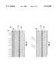
- portion 10includes substrate 16 beneath a gate oxide layer 60 that is beneath a polysilicon and germanium layer 62. Layer 62 is substantially covered with a photoresist layer 64.
- Substrate 16is preferably a silicon substrate, and layer 60 is preferably a gate dielectric layer for dielectric 24 (FIG. 1).
- Layer 60can be thermally grown silicon dioxide.
- Layer 62is exposed to germanium ions through an aperture 72 in photoresist layer 64. The region associated with aperture 72 becomes a polysilicon/germanium material doped with more germanium ions, Si.sub.(1-y) Ge y , (e.g., material 43 (FIG. 4)), where y is greater than x).
- Layer 62is doped or implanted with germanium by an ion implantation technique.
- Layer 62is deposited on top of layer 60 (FIGS. 2 and 3) by chemical vapor deposition (CVD). After deposition, layer 62 can be heavily doped with boron to become a P+ type material and implanted with germanium by the ion implantation process to become material 41 (FIG. 4). Alternatively, layer 62 could be deposited as doped polysilicon with germanium already included.
- Layer 64is preferably photoresist, and a photolithographic technique is utilized to define aperture 72. Aperture 72 is preferably as wide or slightly wider than stack 20 (FIG. 1).
- layer 64is stripped and a protection layer or barrier layer 68 is deposited over layer 62.
- Layer 68can be a silicon oxynitride (SiON) or nitride material.
- Layer 68is preferably deposited under low temperature (e.g., less than 400° C.) by CVD.
- Layer 68protects layer 62 for later source and drain implant steps associated with the formation of transistors 12 and 14.
- Layer 68also advantageously allows a P+ type gate to be utilized for both N-channel and P-channel MOSFETs.
- Layer 68can be doped with boron (P+) when drains 30 and sources 32 are formed for P-channel transistors.
- a photoresist layer 70is deposited and selectively etched in accordance with gate stacks 18 and 20. Portion 10 is plasma-etched or dry-etched to form gate stacks 18 and 20 (FIG. 1 and FIG. 4). In FIG. 4, after etching, layer 70 is removed. Gate stack 18 includes material 41, and gate stack 20 includes material 43. Gate stacks 18 and 20 can be formed by a variety of fabrication techniques. With reference to FIG. 1, conventional transistor processes can be utilized to form drains 30 and sources 32, contacts and interconnectors for portion 10.
- conductors 40 and 42could be doped in accordance with an amorphous silicon process as discussed below with reference to FIGS. 6-9, where a germanium layer is provided on top of a silicon layer. The germanium and silicon layers are subjected to an amorphization process and melted to form conductors 40 and 42 as polysilicon material doped with germanium.
- conductors 40 and 42can be formed in a damascene process as discussed below with reference to FIGS. 15-20. In this process, dummy polysilicon conductors are removed and replaced with polysilicon conductors that are selectively doped with germanium.
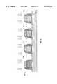
- a portion 200 of an ICincludes transistors 202, 204, 206 and 208 (N-channel or P-channel) which are fabricated in accordance with a similar process described with reference to FIGS. 1-4. Assuming transistor 202, 204, 206, and 208 are N-channel devices, the threshold voltage associated with transistor 202 is lower than the threshold voltages of transistors 204, 206 and 208. The threshold voltage of transistor 204 is higher than the threshold voltages of transistors 206 and 208. Transistor 208 has a higher threshold voltage than transistor 206. Thus, portion 200 includes transistors having four different threshold voltages.
- Threshold voltages of transistor 202, 204, 206, and 208are controlled by the amount of germanium concentration in gate structures 212 associated with transistors 202, 204, 206, and 208. Unlike the process described in FIGS. 1-4, several germanium implantation steps are necessary to appropriately implant gates 212. The implant steps require several photoresist masks to appropriately provide the correct concentrations of germanium in gates 212.
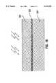
- a polysilicon/germanium film 220can be utilized on portion 10 (FIG. 1) and portion 200 (FIG. 5) as a gate conducting material, such as, materials 41 and 43.
- Film 220is provided over a gate oxide layer 222 that is provided over a silicon substrate 224.
- Film 220is preferably a heavily doped polysilicon/germanium film that can be doped with N-type dopants or P-type dopants. Additionally, film 220 preferably has a box-like dopant profile and is preferably a Si.sub.(1-x) Ge x material, where x is the molar concentration of germanium.
- an amorphous silicon layer 226is deposited by low pressure chemical vapor deposition (LPCVD) on top of layer 222.
- Layer 226is preferably between 100 nm and 200 nm thick and is deposited at a temperature below 500° C.
- Layer 226has a smaller crystal size than film 220 (FIG. 6).
- Layer 222can be a 2-4 nm oxide layer, a 30-50 nm thick nitride layer, or other dielectric layer.
- an amorphous germanium layer 230is deposited by LPCVD over a top surface 238 of layer 226.
- Layer 230is preferably a thin layer of amorphous germanium deposited at a temperature below 500° C.
- layer 230is between 10 and 20 percent of the total thickness of layers 230 and 226 (e.g., between 10 and 40 nm).
- the thickness of layers 226 and 230can be dependent upon the desired composition of film 220 (e.g., the value for x). Accurate control of germanium concentration can be obtained by adjusting the thickness ratio between layers 226 and 230.
- layers 226 and 230are subjected to a dopant implant.
- a dopantsuch as, arsenic, phosphorus, boron, or boron difluoride (BF 2 ), can be implanted about surface 238 (FIG. 7).
- the implantis performed under small implant energy so the projection is relatively shallow below a top surface 236 of layer 230.
- Multiple implants using different types of dopantscan be utilized to increase the dopant concentration within layers 226 and 230, until a level close to the solid solubility limit of layers 226 and 230 is reached.
- the dopantsare preferably implanted in an ion implantation process, wherein the peak of the dopant concentration is centered approximately one-quarter of the thickness of the combination of layers 226 and 230 (e.g., below surface 236 by 25-50 nm).
- the implantis sufficiently shallow to avoid significant dopant tail effect into layer 222.
- layers 226 and 230are subjected to an excimer laser annealing process to melt layers 226 and 230.
- the laser annealing processalso electrically activates dopants in layers 226 and 230 (FIG. 9) at the same time.
- the excimer laser annealing processpreferably heats layers 226 and 230 above the melting point of amorphous silicon (e.g., 900° C.).
- annealingprovides a local temperature above the melting point of amorphous germanium (between approximately 950° C. and 1000° C.).
- film 220is recrystalized as polysilicon with electrically activated impurities.
- the excimer laser annealing processactivates the dopants more quickly than conventional thermal annealing processes.
- other annealing, thermal, or heating processescan be utilized to activate and diffuse dopants.
- the method discussed with reference to FIGS. 6-9advantageously provides a uniform dopant and germanium profile in film 220.
- film 220obtains a uniform box-like dopant profile.
- the evenly distributed germanium profile in film 220is independent of subsequent thermal steps.
- a stable germanium composition near the gate/oxide interfaceis advantageously achieved and gate/depletion effect is minimized.
- a film of a polysilicon film 242is similar to polysilicon/germanium film 220 discussed with reference to FIGS. 6-9.
- File 242can be manufactured in a process similar to the process used to manufacture file 220. However, film 242 does not include germanium.
- Film 242is provided on layer 222, which is provided on substrate 224.
- Film 242has a box-like profile of evenly diffused dopant.
- Film 220can be utilized in portion 10 or portion 50, discussed with reference to FIGS. 1 and 5.
- an amorphous silicon layer 226is deposited by LPCVD on top of layer 222.
- Layer 226is preferably 100 nm-200 nm thick and deposited at a temperature of below 500° C.
- layer 222receives a dopant implant.
- the dopant implantis preferably provided at a shallow projection. Multiple implants can be utilized to increase the dopant concentration until layer 226 is close to its solid solubility limit.
- the dopant regionis centered about the thickness of layer 226, below a top surface 244.
- the dopant implantis sufficiently shallow to avoid dopant tail effect into layer 222 (approximately 25 to 50 nm below surface 244).
- layer 226(FIG. 9) is subject to excimer laser annealing to melt layer 226.
- the excimer laser annealingdiffuses dopant evenly through film 242 in a box-like profile.
- the excimer laser annealingpreferably provides a local temperature between 900° C. and 1000° C. for film 242, thereby activating electrically activating dopants.
- Film 242is recrystalized as polysilicon after heating. Alternatively, films 220 and 242 could be heated by other processes to activate dopants and recrystalize films 220 and 242.
- a portion 310 of an IC or chipincludes a transistor 312 and a transistor 314.
- Portion 310is preferably part of a ULSI circuit and can be similar to portion 10 (FIG. 1).
- Transistors 312 and 314are disposed on a substrate 316 that is preferably silicon.
- Transistor 312includes a gate stack 318
- transistor 314includes a gate stack 320.
- Each of gate stack 318 and gate stack 320includes sidewall spacers 322, a gate dielectric 324, and a protection layer 326.
- Protection layer 326is preferably a SiO x N y layer that is utilized as a polish stopper.
- An insulative layer 323is deposited over protection layer 326.
- Layer 323can be silicon dioxide deposited in a tetraorthosilicate (TEOS) process.
- TEOStetraorthosilicate
- Transistors 312 and 314both include a drain 330, a source 332, and a channel 334.
- Channel 334 of transistor 312has almost identical characteristics to channel 334 of transistor 314.
- Transistors 312 and 314are made with the same identical channel implant to avoid short channel performance degradation and can be similar to transistors 12 and 14 (FIG. 1).
- Transistors 310 and 312are separated by shallow isolation trenches 321.
- Gate stack 318includes a gate conductor 340, and gate stack 320 includes a gate conductor 342.
- Gate conductors 340 and 342are preferably manufactured from a semiconductor material, such as, polysilicon, and are both implanted with another semiconductor material, such as, germanium. Gate conductors 340 and 342 are also heavily doped with a P-type dopant, such as, boron. Gate conductor 340 has a higher concentration of germanium than gate conductor 342, as indicated by the lighter shading of gate conductor 342.
- transistors 312 and 314are P-channel MOSFETs, transistor 314 has a lower threshold voltage than transistor 312 due to the lower concentration of germanium in conductor 342. If transistors 312 and 314 are N-channel transistors, transistor 314 has a higher threshold voltage due to the higher concentration of germanium in conductor 340.
- Transistors 312 and 314can have similar exemplary values as described with reference to transistors 12 and 14 in FIGS. 1-5.
- portion 310includes transistors 312 and 314 having dummy gate structures or stacks 350.
- the damascene processallows a self-aligned technique to be utilized because sources 332 and drains 334 are formed with stacks 350.
- Dummy gate stacks 350include an undoped polysilicon material 356, dielectric 324, and spacers 322.
- material 356can be other types of semiconductor materials.
- Stacks 350are covered by a barrier layer 326 made of siliconoxynitride (SiO x N y ), which is overcoated by an insulative layer 323.
- Layer 323can be an oxide layer.
- Transistors 312 and 314, including stacks 350can be fabricated according to conventional processes.
- portion 310is subject to a chemical-mechanical polish (CMP) to remove a portion of insulative layer 323. Portion 310 is subject to the CMP until layer 352 is removed from the top of dummy stacks 350.
- CMPchemical-mechanical polish
- polysilicon material 356is removed by wet etching selective to polysilicon. Alternatively, dry-etching or other stripping techniques can be utilized to remove polysilicon material 356 from dummy stacks 350.
- gate conductors 340 and 342are provided in-situ for transistors 312 and 314.
- P+-type doped polysilicon/germaniumis deposited and etched back to leave a form of conductors 340 and 342 between spacers 322.
- polysiliconcan be deposited and implanted with germanium.
- transistor 314is covered by a photoresist layer 362.
- gate conductor 340 associated with transistor 312is implanted with germanium ions to a concentration so that conductor 340 is composed of a Si.sub.(1-y) Ge y , material, and conductor 342 is composed of a Si.sub.(1-x) Ge x material, where y is greater than x.
- conductors 340 and 342can be provided as undoped polysilicon and doped in subsequent steps.
- a photoresist layer similar to layer 362can be provided over transistor 314 and ion (e.g., germanium) implantation can be provided to conductor 342.
- conductors 340 and 342can be provided as films 220 and 242 (FIG. 6 and FIG. 10, respectively).
Landscapes
- Metal-Oxide And Bipolar Metal-Oxide Semiconductor Integrated Circuits (AREA)
Abstract
Description
Claims (20)
Priority Applications (1)
| Application Number | Priority Date | Filing Date | Title |
|---|---|---|---|
| US09/187,171US6114206A (en) | 1998-11-06 | 1998-11-06 | Multiple threshold voltage transistor implemented by a damascene process |
Applications Claiming Priority (1)
| Application Number | Priority Date | Filing Date | Title |
|---|---|---|---|
| US09/187,171US6114206A (en) | 1998-11-06 | 1998-11-06 | Multiple threshold voltage transistor implemented by a damascene process |
Publications (1)
| Publication Number | Publication Date |
|---|---|
| US6114206Atrue US6114206A (en) | 2000-09-05 |
Family
ID=22687878
Family Applications (1)
| Application Number | Title | Priority Date | Filing Date |
|---|---|---|---|
| US09/187,171Expired - LifetimeUS6114206A (en) | 1998-11-06 | 1998-11-06 | Multiple threshold voltage transistor implemented by a damascene process |
Country Status (1)
| Country | Link |
|---|---|
| US (1) | US6114206A (en) |
Cited By (37)
| Publication number | Priority date | Publication date | Assignee | Title |
|---|---|---|---|---|
| US6248001B1 (en)* | 1999-08-06 | 2001-06-19 | Micron Technology, Inc. | Semiconductor die de-processing using a die holder and chemical mechanical polishing |
| US6258679B1 (en)* | 1999-12-20 | 2001-07-10 | International Business Machines Corporation | Sacrificial silicon sidewall for damascene gate formation |
| EP1134795A1 (en)* | 2000-03-17 | 2001-09-19 | Infineon Technologies AG | Method of adjusting the threshold voltage of a MOS transistor |
| US6365463B2 (en)* | 1999-05-21 | 2002-04-02 | Nat Semiconductor Corp | Method for forming a high-precision analog transistor with a low threshold voltage roll-up and a digital transistor with a high threshold voltage roll-up |
| US6514824B1 (en)* | 1998-09-29 | 2003-02-04 | Lsi Logic Corporation | Semiconductor device with a pair of transistors having dual work function gate electrodes |
| US20030052354A1 (en)* | 2000-11-27 | 2003-03-20 | Dennison Charles H. | Use of gate electrode workfunction to improve DRAM refresh |
| US6645818B1 (en) | 2002-11-13 | 2003-11-11 | Chartered Semiconductor Manufacturing Ltd. | Method to fabricate dual-metal gate for N- and P-FETs |
| DE10233421A1 (en)* | 2002-06-06 | 2004-02-12 | Promos Technologies, Inc. | Forming dual-implanted gate |
| US20040104440A1 (en)* | 2002-06-06 | 2004-06-03 | Benny Yen | [method of forming dual-implanted gate and structure formed by the same] |
| US20040157383A1 (en)* | 2002-07-26 | 2004-08-12 | Park Jeong Ho | Method for forming short-channel transistors |
| US6818952B2 (en) | 2002-10-01 | 2004-11-16 | International Business Machines Corporation | Damascene gate multi-mesa MOSFET |
| US20060003558A1 (en)* | 2004-06-30 | 2006-01-05 | Dongbuanam Semiconductor Inc. | Method for fabricating semiconductor device and semiconductor device using the same |
| US20060068539A1 (en)* | 2004-09-14 | 2006-03-30 | Byung-Jun Park | Method of fabricating CMOS type semiconductor device having dual gates |
| US20060148175A1 (en)* | 2004-12-30 | 2006-07-06 | Dongbuanam Semiconductor Inc. | Method of manufacturing a flash memory device |
| US20070105295A1 (en)* | 2005-11-08 | 2007-05-10 | Dongbuanam Semiconductor Inc. | Method for forming lightly-doped-drain metal-oxide-semiconductor (LDD MOS) device |
| US20080169512A1 (en)* | 2004-08-10 | 2008-07-17 | Doyle Brian S | Non-planar pMOS structure with a strained channel region and an integrated strained CMOS flow |
| US20090061572A1 (en)* | 2003-06-27 | 2009-03-05 | Intel Corporation | Nonplanar semiconductor device with partially or fully wrapped around gate electrode and methods of fabrication |
| US7736956B2 (en) | 2005-08-17 | 2010-06-15 | Intel Corporation | Lateral undercut of metal gate in SOI device |
| US20100200917A1 (en)* | 2003-06-27 | 2010-08-12 | Hareland Scott A | Nonplanar device with stress incorporation layer and method of fabrication |
| US7781771B2 (en) | 2004-03-31 | 2010-08-24 | Intel Corporation | Bulk non-planar transistor having strained enhanced mobility and methods of fabrication |
| US7858481B2 (en)* | 2005-06-15 | 2010-12-28 | Intel Corporation | Method for fabricating transistor with thinned channel |
| US7879675B2 (en) | 2005-03-14 | 2011-02-01 | Intel Corporation | Field effect transistor with metal source/drain regions |
| US7898041B2 (en) | 2005-06-30 | 2011-03-01 | Intel Corporation | Block contact architectures for nanoscale channel transistors |
| US7902014B2 (en) | 2005-09-28 | 2011-03-08 | Intel Corporation | CMOS devices with a single work function gate electrode and method of fabrication |
| US7989280B2 (en) | 2005-11-30 | 2011-08-02 | Intel Corporation | Dielectric interface for group III-V semiconductor device |
| US8067818B2 (en) | 2004-10-25 | 2011-11-29 | Intel Corporation | Nonplanar device with thinned lower body portion and method of fabrication |
| US8071983B2 (en) | 2005-06-21 | 2011-12-06 | Intel Corporation | Semiconductor device structures and methods of forming semiconductor structures |
| US8084818B2 (en) | 2004-06-30 | 2011-12-27 | Intel Corporation | High mobility tri-gate devices and methods of fabrication |
| US8183646B2 (en) | 2005-02-23 | 2012-05-22 | Intel Corporation | Field effect transistor with narrow bandgap source and drain regions and method of fabrication |
| US8268709B2 (en) | 2004-09-29 | 2012-09-18 | Intel Corporation | Independently accessed double-gate and tri-gate transistors in same process flow |
| US8362566B2 (en) | 2008-06-23 | 2013-01-29 | Intel Corporation | Stress in trigate devices using complimentary gate fill materials |
| US8617945B2 (en) | 2006-08-02 | 2013-12-31 | Intel Corporation | Stacking fault and twin blocking barrier for integrating III-V on Si |
| CN103545181A (en)* | 2012-07-11 | 2014-01-29 | 中芯国际集成电路制造(上海)有限公司 | A method of manufacturing a semiconductor device using a dummy gate |
| CN103545185A (en)* | 2012-07-13 | 2014-01-29 | 中芯国际集成电路制造(上海)有限公司 | A method of manufacturing semiconductor devices using dummy gates |
| US20140203375A1 (en)* | 2010-03-16 | 2014-07-24 | Taiwan Semiconductor Manufacturing Company, Ltd. | Reduced Substrate Coupling for Inductors in Semiconductor Devices |
| US20140227845A1 (en)* | 2013-02-14 | 2014-08-14 | Globalfoundries Inc. | Methods of forming multiple n-type semiconductor devices with different threshold voltages on a semiconductor substrate |
| US10361301B2 (en) | 2016-03-31 | 2019-07-23 | International Business Machines Corporation | Fabrication of vertical fin transistor with multiple threshold voltages |
Citations (13)
| Publication number | Priority date | Publication date | Assignee | Title |
|---|---|---|---|---|
| US4137103A (en)* | 1976-12-06 | 1979-01-30 | International Business Machines Corporation | Silicon integrated circuit region containing implanted arsenic and germanium |
| US4728619A (en)* | 1987-06-19 | 1988-03-01 | Motorola, Inc. | Field implant process for CMOS using germanium |
| US5426069A (en)* | 1992-04-09 | 1995-06-20 | Dalsa Inc. | Method for making silicon-germanium devices using germanium implantation |
| US5576574A (en)* | 1995-06-30 | 1996-11-19 | United Microelectronics Corporation | Mosfet with fully overlapped lightly doped drain structure and method for manufacturing same |
| US5786256A (en)* | 1996-07-19 | 1998-07-28 | Advanced Micro Devices, Inc. | Method of reducing MOS transistor gate beyond photolithographically patterned dimension |
| US5937297A (en)* | 1998-06-01 | 1999-08-10 | Chartered Semiconductor Manufacturing, Ltd. | Method for making sub-quarter-micron MOSFET |
| US5952701A (en)* | 1997-08-18 | 1999-09-14 | National Semiconductor Corporation | Design and fabrication of semiconductor structure having complementary channel-junction insulated-gate field-effect transistors whose gate electrodes have work functions close to mid-gap semiconductor value |
| US5953615A (en)* | 1999-01-27 | 1999-09-14 | Advance Micro Devices | Pre-amorphization process for source/drain junction |
| US5960270A (en)* | 1997-08-11 | 1999-09-28 | Motorola, Inc. | Method for forming an MOS transistor having a metallic gate electrode that is formed after the formation of self-aligned source and drain regions |
| US5985726A (en)* | 1998-11-06 | 1999-11-16 | Advanced Micro Devices, Inc. | Damascene process for forming ultra-shallow source/drain extensions and pocket in ULSI MOSFET |
| US5998271A (en)* | 1995-07-18 | 1999-12-07 | Siemens Aktiengesellschaft | Method of producing an MOS transistor |
| US6001698A (en)* | 1996-04-30 | 1999-12-14 | Sony Corporation | MOS transistor and fabrication process for the same |
| US6008111A (en)* | 1996-03-15 | 1999-12-28 | Fujitsu Limited | Method of manufacturing semiconductor device |
- 1998
- 1998-11-06USUS09/187,171patent/US6114206A/ennot_activeExpired - Lifetime
Patent Citations (13)
| Publication number | Priority date | Publication date | Assignee | Title |
|---|---|---|---|---|
| US4137103A (en)* | 1976-12-06 | 1979-01-30 | International Business Machines Corporation | Silicon integrated circuit region containing implanted arsenic and germanium |
| US4728619A (en)* | 1987-06-19 | 1988-03-01 | Motorola, Inc. | Field implant process for CMOS using germanium |
| US5426069A (en)* | 1992-04-09 | 1995-06-20 | Dalsa Inc. | Method for making silicon-germanium devices using germanium implantation |
| US5576574A (en)* | 1995-06-30 | 1996-11-19 | United Microelectronics Corporation | Mosfet with fully overlapped lightly doped drain structure and method for manufacturing same |
| US5998271A (en)* | 1995-07-18 | 1999-12-07 | Siemens Aktiengesellschaft | Method of producing an MOS transistor |
| US6008111A (en)* | 1996-03-15 | 1999-12-28 | Fujitsu Limited | Method of manufacturing semiconductor device |
| US6001698A (en)* | 1996-04-30 | 1999-12-14 | Sony Corporation | MOS transistor and fabrication process for the same |
| US5786256A (en)* | 1996-07-19 | 1998-07-28 | Advanced Micro Devices, Inc. | Method of reducing MOS transistor gate beyond photolithographically patterned dimension |
| US5960270A (en)* | 1997-08-11 | 1999-09-28 | Motorola, Inc. | Method for forming an MOS transistor having a metallic gate electrode that is formed after the formation of self-aligned source and drain regions |
| US5952701A (en)* | 1997-08-18 | 1999-09-14 | National Semiconductor Corporation | Design and fabrication of semiconductor structure having complementary channel-junction insulated-gate field-effect transistors whose gate electrodes have work functions close to mid-gap semiconductor value |
| US5937297A (en)* | 1998-06-01 | 1999-08-10 | Chartered Semiconductor Manufacturing, Ltd. | Method for making sub-quarter-micron MOSFET |
| US5985726A (en)* | 1998-11-06 | 1999-11-16 | Advanced Micro Devices, Inc. | Damascene process for forming ultra-shallow source/drain extensions and pocket in ULSI MOSFET |
| US5953615A (en)* | 1999-01-27 | 1999-09-14 | Advance Micro Devices | Pre-amorphization process for source/drain junction |
Non-Patent Citations (16)
| Title |
|---|
| Kiing et al, "A variable work function polycrystalline Si(1-x)Ge(x) Gate material for submicrometer CMOS technologies," IEEE Elect. Dev. Lett., vol. 12, No. 10, p. 533, Oct. 1991. |
| Kiing et al, A variable work function polycrystalline Si(1 x)Ge(x) Gate material for submicrometer CMOS technologies, IEEE Elect. Dev. Lett., vol. 12, No. 10, p. 533, Oct. 1991.* |
| King et al "A polycrystalline Si(1-x)Ge(x) gate CMOS technology," IEEE IEDM 90, p. 253, 1990. |
| King et al A polycrystalline Si(1 x)Ge(x) gate CMOS technology, IEEE IEDM 90, p. 253, 1990.* |
| Lee et al, "Optimized poly-Si(1-x)Ge(x) gate technology for dual gate CMOS application," IEEE Symp. on VLSI Techn. Dig. of Tech. Papers, p. 190, 1998. |
| Lee et al, Optimized poly Si(1 x)Ge(x) gate technology for dual gate CMOS application, IEEE Symp. on VLSI Techn. Dig. of Tech. Papers, p. 190, 1998.* |
| Lee, et al, "Investigation of poly-Si(1-x)Ge(x) for dual gate CMOS technology," IEEE Elect. Dev. Lett., vol. 19, No. 7, p. 247, Jul. 1998. |
| Lee, et al, Investigation of poly Si(1 x)Ge(x) for dual gate CMOS technology, IEEE Elect. Dev. Lett., vol. 19, No. 7, p. 247, Jul. 1998.* |
| Salm et al, "Gate current and oxide reliability in p+ poly MOS capacitors with poly-Si and poly Ge(O.3)Si(0.7) gate material," IEEE Elect. Dev. Lett., vol. 19, No. 7, p. 213, Jul. 1998. |
| Salm et al, Gate current and oxide reliability in p poly MOS capacitors with poly Si and poly Ge(O.3)Si(0.7) gate material, IEEE Elect. Dev. Lett., vol. 19, No. 7, p. 213, Jul. 1998.* |
| Tang et al, "A novel poly silicon capped poly-silicon-germanium thin-film tansistor," IEEE IEDM 95, p. 513, 1995. |
| Tang et al, A novel poly silicon capped poly silicon germanium thin film tansistor, IEEE IEDM 95, p. 513, 1995.* |
| Yu et al "Gate engineering for deep submicron CMOS transistors," IEEE Trans. on Elec. Dev., vol. 45, No. 6, p. 1253, Jun. 1998. |
| Yu et al Gate engineering for deep submicron CMOS transistors, IEEE Trans. on Elec. Dev., vol. 45, No. 6, p. 1253, Jun. 1998.* |
| Yu et al, "Gate engineering for performance and reliability in deep submicron CMOS technology," 1997 Symp. on VLSI Tech. Dig. of Tech. Papers, p. 105, 1997. |
| Yu et al, Gate engineering for performance and reliability in deep submicron CMOS technology, 1997 Symp. on VLSI Tech. Dig. of Tech. Papers, p. 105, 1997.* |
Cited By (88)
| Publication number | Priority date | Publication date | Assignee | Title |
|---|---|---|---|---|
| US6514824B1 (en)* | 1998-09-29 | 2003-02-04 | Lsi Logic Corporation | Semiconductor device with a pair of transistors having dual work function gate electrodes |
| US6365463B2 (en)* | 1999-05-21 | 2002-04-02 | Nat Semiconductor Corp | Method for forming a high-precision analog transistor with a low threshold voltage roll-up and a digital transistor with a high threshold voltage roll-up |
| US6248001B1 (en)* | 1999-08-06 | 2001-06-19 | Micron Technology, Inc. | Semiconductor die de-processing using a die holder and chemical mechanical polishing |
| US20010037863A1 (en)* | 1999-08-06 | 2001-11-08 | Carson Bryan C. | Semiconductor die de-processing using a die holder and chemical mechanical polishing |
| US6921318B2 (en) | 1999-08-06 | 2005-07-26 | Micron Technology, Inc. | Semiconductor die de-processing using a die holder and chemical mechanical polishing |
| US6258679B1 (en)* | 1999-12-20 | 2001-07-10 | International Business Machines Corporation | Sacrificial silicon sidewall for damascene gate formation |
| EP1134795A1 (en)* | 2000-03-17 | 2001-09-19 | Infineon Technologies AG | Method of adjusting the threshold voltage of a MOS transistor |
| US6451676B2 (en) | 2000-03-17 | 2002-09-17 | Infineon Technologies Ag | Method for setting the threshold voltage of a MOS transistor |
| US6924190B2 (en)* | 2000-11-27 | 2005-08-02 | Micron Technology, Inc. | Use of gate electrode workfunction to improve DRAM refresh |
| US20030052354A1 (en)* | 2000-11-27 | 2003-03-20 | Dennison Charles H. | Use of gate electrode workfunction to improve DRAM refresh |
| US20050173746A1 (en)* | 2000-11-27 | 2005-08-11 | Dennison Charles H. | Use of gate electrode workfunction to improve DRAM refresh |
| US7355203B2 (en) | 2000-11-27 | 2008-04-08 | Micron Technology, Inc. | Use of gate electrode workfunction to improve DRAM refresh |
| DE10233421A1 (en)* | 2002-06-06 | 2004-02-12 | Promos Technologies, Inc. | Forming dual-implanted gate |
| US20040104440A1 (en)* | 2002-06-06 | 2004-06-03 | Benny Yen | [method of forming dual-implanted gate and structure formed by the same] |
| DE10233421B4 (en)* | 2002-06-06 | 2006-03-02 | Promos Technologies, Inc. | Method for forming a double-implanted gate |
| US20040157383A1 (en)* | 2002-07-26 | 2004-08-12 | Park Jeong Ho | Method for forming short-channel transistors |
| US6998318B2 (en)* | 2002-07-26 | 2006-02-14 | Dongbuanam Semiconductor Inc. | Method for forming short-channel transistors |
| US6818952B2 (en) | 2002-10-01 | 2004-11-16 | International Business Machines Corporation | Damascene gate multi-mesa MOSFET |
| US20050012145A1 (en)* | 2002-10-01 | 2005-01-20 | International Business Machines Corporation | Damascene gate multi-mesa MOSFET |
| US7081387B2 (en) | 2002-10-01 | 2006-07-25 | International Business Machines Corporation | Damascene gate multi-mesa MOSFET |
| US6645818B1 (en) | 2002-11-13 | 2003-11-11 | Chartered Semiconductor Manufacturing Ltd. | Method to fabricate dual-metal gate for N- and P-FETs |
| US20100200917A1 (en)* | 2003-06-27 | 2010-08-12 | Hareland Scott A | Nonplanar device with stress incorporation layer and method of fabrication |
| US8273626B2 (en) | 2003-06-27 | 2012-09-25 | Intel Corporationn | Nonplanar semiconductor device with partially or fully wrapped around gate electrode and methods of fabrication |
| US20090061572A1 (en)* | 2003-06-27 | 2009-03-05 | Intel Corporation | Nonplanar semiconductor device with partially or fully wrapped around gate electrode and methods of fabrication |
| US8405164B2 (en) | 2003-06-27 | 2013-03-26 | Intel Corporation | Tri-gate transistor device with stress incorporation layer and method of fabrication |
| US7820513B2 (en) | 2003-06-27 | 2010-10-26 | Intel Corporation | Nonplanar semiconductor device with partially or fully wrapped around gate electrode and methods of fabrication |
| US7781771B2 (en) | 2004-03-31 | 2010-08-24 | Intel Corporation | Bulk non-planar transistor having strained enhanced mobility and methods of fabrication |
| US7271078B2 (en) | 2004-06-30 | 2007-09-18 | Dongbu Electronics Co., Ltd. | Method for fabricating semiconductor device and semiconductor device using the same |
| US20060003558A1 (en)* | 2004-06-30 | 2006-01-05 | Dongbuanam Semiconductor Inc. | Method for fabricating semiconductor device and semiconductor device using the same |
| US8084818B2 (en) | 2004-06-30 | 2011-12-27 | Intel Corporation | High mobility tri-gate devices and methods of fabrication |
| US20080169512A1 (en)* | 2004-08-10 | 2008-07-17 | Doyle Brian S | Non-planar pMOS structure with a strained channel region and an integrated strained CMOS flow |
| US7960794B2 (en) | 2004-08-10 | 2011-06-14 | Intel Corporation | Non-planar pMOS structure with a strained channel region and an integrated strained CMOS flow |
| US20060068539A1 (en)* | 2004-09-14 | 2006-03-30 | Byung-Jun Park | Method of fabricating CMOS type semiconductor device having dual gates |
| US7192822B2 (en) | 2004-09-14 | 2007-03-20 | Samsung Electronics Co., Ltd. | Method of fabricating CMOS type semiconductor device having dual gates |
| US8268709B2 (en) | 2004-09-29 | 2012-09-18 | Intel Corporation | Independently accessed double-gate and tri-gate transistors in same process flow |
| US8399922B2 (en) | 2004-09-29 | 2013-03-19 | Intel Corporation | Independently accessed double-gate and tri-gate transistors |
| US10236356B2 (en) | 2004-10-25 | 2019-03-19 | Intel Corporation | Nonplanar device with thinned lower body portion and method of fabrication |
| US9741809B2 (en) | 2004-10-25 | 2017-08-22 | Intel Corporation | Nonplanar device with thinned lower body portion and method of fabrication |
| US9190518B2 (en) | 2004-10-25 | 2015-11-17 | Intel Corporation | Nonplanar device with thinned lower body portion and method of fabrication |
| US8067818B2 (en) | 2004-10-25 | 2011-11-29 | Intel Corporation | Nonplanar device with thinned lower body portion and method of fabrication |
| US8749026B2 (en) | 2004-10-25 | 2014-06-10 | Intel Corporation | Nonplanar device with thinned lower body portion and method of fabrication |
| US8502351B2 (en) | 2004-10-25 | 2013-08-06 | Intel Corporation | Nonplanar device with thinned lower body portion and method of fabrication |
| US20060148175A1 (en)* | 2004-12-30 | 2006-07-06 | Dongbuanam Semiconductor Inc. | Method of manufacturing a flash memory device |
| US9748391B2 (en) | 2005-02-23 | 2017-08-29 | Intel Corporation | Field effect transistor with narrow bandgap source and drain regions and method of fabrication |
| US8664694B2 (en) | 2005-02-23 | 2014-03-04 | Intel Corporation | Field effect transistor with narrow bandgap source and drain regions and method of fabrication |
| US10121897B2 (en) | 2005-02-23 | 2018-11-06 | Intel Corporation | Field effect transistor with narrow bandgap source and drain regions and method of fabrication |
| US8368135B2 (en) | 2005-02-23 | 2013-02-05 | Intel Corporation | Field effect transistor with narrow bandgap source and drain regions and method of fabrication |
| US9614083B2 (en) | 2005-02-23 | 2017-04-04 | Intel Corporation | Field effect transistor with narrow bandgap source and drain regions and method of fabrication |
| US8183646B2 (en) | 2005-02-23 | 2012-05-22 | Intel Corporation | Field effect transistor with narrow bandgap source and drain regions and method of fabrication |
| US9368583B2 (en) | 2005-02-23 | 2016-06-14 | Intel Corporation | Field effect transistor with narrow bandgap source and drain regions and method of fabrication |
| US9048314B2 (en) | 2005-02-23 | 2015-06-02 | Intel Corporation | Field effect transistor with narrow bandgap source and drain regions and method of fabrication |
| US8816394B2 (en) | 2005-02-23 | 2014-08-26 | Intel Corporation | Field effect transistor with narrow bandgap source and drain regions and method of fabrication |
| US7879675B2 (en) | 2005-03-14 | 2011-02-01 | Intel Corporation | Field effect transistor with metal source/drain regions |
| US9806195B2 (en) | 2005-06-15 | 2017-10-31 | Intel Corporation | Method for fabricating transistor with thinned channel |
| US9337307B2 (en) | 2005-06-15 | 2016-05-10 | Intel Corporation | Method for fabricating transistor with thinned channel |
| US11978799B2 (en) | 2005-06-15 | 2024-05-07 | Tahoe Research, Ltd. | Method for fabricating transistor with thinned channel |
| US10937907B2 (en) | 2005-06-15 | 2021-03-02 | Intel Corporation | Method for fabricating transistor with thinned channel |
| US7858481B2 (en)* | 2005-06-15 | 2010-12-28 | Intel Corporation | Method for fabricating transistor with thinned channel |
| US10367093B2 (en) | 2005-06-15 | 2019-07-30 | Intel Corporation | Method for fabricating transistor with thinned channel |
| US8933458B2 (en) | 2005-06-21 | 2015-01-13 | Intel Corporation | Semiconductor device structures and methods of forming semiconductor structures |
| US8581258B2 (en) | 2005-06-21 | 2013-11-12 | Intel Corporation | Semiconductor device structures and methods of forming semiconductor structures |
| US9761724B2 (en) | 2005-06-21 | 2017-09-12 | Intel Corporation | Semiconductor device structures and methods of forming semiconductor structures |
| US8071983B2 (en) | 2005-06-21 | 2011-12-06 | Intel Corporation | Semiconductor device structures and methods of forming semiconductor structures |
| US9385180B2 (en) | 2005-06-21 | 2016-07-05 | Intel Corporation | Semiconductor device structures and methods of forming semiconductor structures |
| US7898041B2 (en) | 2005-06-30 | 2011-03-01 | Intel Corporation | Block contact architectures for nanoscale channel transistors |
| US7736956B2 (en) | 2005-08-17 | 2010-06-15 | Intel Corporation | Lateral undercut of metal gate in SOI device |
| US8294180B2 (en) | 2005-09-28 | 2012-10-23 | Intel Corporation | CMOS devices with a single work function gate electrode and method of fabrication |
| US7902014B2 (en) | 2005-09-28 | 2011-03-08 | Intel Corporation | CMOS devices with a single work function gate electrode and method of fabrication |
| US20070105295A1 (en)* | 2005-11-08 | 2007-05-10 | Dongbuanam Semiconductor Inc. | Method for forming lightly-doped-drain metal-oxide-semiconductor (LDD MOS) device |
| US7989280B2 (en) | 2005-11-30 | 2011-08-02 | Intel Corporation | Dielectric interface for group III-V semiconductor device |
| US8617945B2 (en) | 2006-08-02 | 2013-12-31 | Intel Corporation | Stacking fault and twin blocking barrier for integrating III-V on Si |
| US9450092B2 (en) | 2008-06-23 | 2016-09-20 | Intel Corporation | Stress in trigate devices using complimentary gate fill materials |
| US8362566B2 (en) | 2008-06-23 | 2013-01-29 | Intel Corporation | Stress in trigate devices using complimentary gate fill materials |
| US9224754B2 (en) | 2008-06-23 | 2015-12-29 | Intel Corporation | Stress in trigate devices using complimentary gate fill materials |
| US9806193B2 (en) | 2008-06-23 | 2017-10-31 | Intel Corporation | Stress in trigate devices using complimentary gate fill materials |
| US8741733B2 (en) | 2008-06-23 | 2014-06-03 | Intel Corporation | Stress in trigate devices using complimentary gate fill materials |
| US20140203375A1 (en)* | 2010-03-16 | 2014-07-24 | Taiwan Semiconductor Manufacturing Company, Ltd. | Reduced Substrate Coupling for Inductors in Semiconductor Devices |
| US9196611B2 (en)* | 2010-03-16 | 2015-11-24 | Taiwan Semiconductor Manufacturing Company, Ltd. | Reduced substrate coupling for inductors in semiconductor devices |
| CN103545181B (en)* | 2012-07-11 | 2017-06-16 | 中芯国际集成电路制造(上海)有限公司 | A kind of method that use dummy gate electrode manufactures semiconductor devices |
| CN103545181A (en)* | 2012-07-11 | 2014-01-29 | 中芯国际集成电路制造(上海)有限公司 | A method of manufacturing a semiconductor device using a dummy gate |
| CN103545185A (en)* | 2012-07-13 | 2014-01-29 | 中芯国际集成电路制造(上海)有限公司 | A method of manufacturing semiconductor devices using dummy gates |
| CN103545185B (en)* | 2012-07-13 | 2017-06-13 | 中芯国际集成电路制造(上海)有限公司 | A kind of method that use dummy grid manufactures semiconductor devices |
| US20140227845A1 (en)* | 2013-02-14 | 2014-08-14 | Globalfoundries Inc. | Methods of forming multiple n-type semiconductor devices with different threshold voltages on a semiconductor substrate |
| US8846476B2 (en)* | 2013-02-14 | 2014-09-30 | Globalfoundries Inc. | Methods of forming multiple N-type semiconductor devices with different threshold voltages on a semiconductor substrate |
| US10361301B2 (en) | 2016-03-31 | 2019-07-23 | International Business Machines Corporation | Fabrication of vertical fin transistor with multiple threshold voltages |
| US10991823B2 (en) | 2016-03-31 | 2021-04-27 | International Business Machines Corporation | Fabrication of vertical fin transistor with multiple threshold voltages |
| US11018254B2 (en) | 2016-03-31 | 2021-05-25 | International Business Machines Corporation | Fabrication of vertical fin transistor with multiple threshold voltages |
| US11043587B2 (en) | 2016-03-31 | 2021-06-22 | International Business Machines Corporation | Fabrication of vertical fin transistor with multiple threshold voltages |
Similar Documents
| Publication | Publication Date | Title |
|---|---|---|
| US6114206A (en) | Multiple threshold voltage transistor implemented by a damascene process | |
| US6262456B1 (en) | Integrated circuit having transistors with different threshold voltages | |
| US6281559B1 (en) | Gate stack structure for variable threshold voltage | |
| US6124610A (en) | Isotropically etching sidewall spacers to be used for both an NMOS source/drain implant and a PMOS LDD implant | |
| US4319395A (en) | Method of making self-aligned device | |
| US7348636B2 (en) | CMOS transistor having different PMOS and NMOS gate electrode structures and method of fabrication thereof | |
| US6693333B1 (en) | Semiconductor-on-insulator circuit with multiple work functions | |
| US4603468A (en) | Method for source/drain self-alignment in stacked CMOS | |
| US6033944A (en) | Semiconductor device and semiconductor device manufacturing method | |
| US4760033A (en) | Method for the manufacture of complementary MOS field effect transistors in VLSI technology | |
| US6096591A (en) | Method of making an IGFET and a protected resistor with reduced processing steps | |
| US20010016389A1 (en) | Channel implant through gate polysilicon | |
| KR20080086484A (en) | Fabrication and Operation Method of Low Power Junction Field Effect Transistor | |
| JP4260905B2 (en) | Method for manufacturing an integrated circuit | |
| US6051487A (en) | Semiconductor device fabrication using a sacrificial plug for defining a region for a gate electrode | |
| WO1998008253A1 (en) | Dual gate oxide thickness integrated circuit and process for making same | |
| US6214681B1 (en) | Process for forming polysilicon/germanium thin films without germanium outgassing | |
| US6127216A (en) | Heavily-doped polysilicon/germanium thin film formed by laser annealing | |
| US6190952B1 (en) | Multiple semiconductor-on-insulator threshold voltage circuit | |
| US6140163A (en) | Method and apparatus for upper level substrate isolation integrated with bulk silicon | |
| US6020260A (en) | Method of fabricating a semiconductor device having nitrogen-bearing gate electrode | |
| US6376323B1 (en) | Fabrication of gate of P-channel field effect transistor with added implantation before patterning of the gate | |
| US6207482B1 (en) | Integration method for deep sub-micron dual gate transistor design | |
| US5494843A (en) | Method for forming MOSFET devices | |
| US6027964A (en) | Method of making an IGFET with a selectively doped gate in combination with a protected resistor |
Legal Events
| Date | Code | Title | Description |
|---|---|---|---|
| AS | Assignment | Owner name:ADVANCED MICRO DEVICES, INC., CALIFORNIA Free format text:ASSIGNMENT OF ASSIGNORS INTEREST;ASSIGNOR:YU, BIN;REEL/FRAME:009571/0775 Effective date:19981019 | |
| STCF | Information on status: patent grant | Free format text:PATENTED CASE | |
| FPAY | Fee payment | Year of fee payment:4 | |
| FEPP | Fee payment procedure | Free format text:PAYOR NUMBER ASSIGNED (ORIGINAL EVENT CODE: ASPN); ENTITY STATUS OF PATENT OWNER: LARGE ENTITY | |
| FPAY | Fee payment | Year of fee payment:8 | |
| AS | Assignment | Owner name:GLOBALFOUNDRIES INC., CAYMAN ISLANDS Free format text:AFFIRMATION OF PATENT ASSIGNMENT;ASSIGNOR:ADVANCED MICRO DEVICES, INC.;REEL/FRAME:023119/0083 Effective date:20090630 | |
| FPAY | Fee payment | Year of fee payment:12 | |
| AS | Assignment | Owner name:WILMINGTON TRUST, NATIONAL ASSOCIATION, DELAWARE Free format text:SECURITY AGREEMENT;ASSIGNOR:GLOBALFOUNDRIES INC.;REEL/FRAME:049490/0001 Effective date:20181127 | |
| AS | Assignment | Owner name:GLOBALFOUNDRIES INC., CAYMAN ISLANDS Free format text:RELEASE BY SECURED PARTY;ASSIGNOR:WILMINGTON TRUST, NATIONAL ASSOCIATION;REEL/FRAME:054636/0001 Effective date:20201117 | |
| AS | Assignment | Owner name:GLOBALFOUNDRIES U.S. INC., NEW YORK Free format text:RELEASE BY SECURED PARTY;ASSIGNOR:WILMINGTON TRUST, NATIONAL ASSOCIATION;REEL/FRAME:056987/0001 Effective date:20201117 |