US6114082A - Frequency doubling hybrid photoresist having negative and positive tone components and method of preparing the same - Google Patents
Frequency doubling hybrid photoresist having negative and positive tone components and method of preparing the sameDownload PDFInfo
- Publication number
- US6114082A US6114082AUS08/715,287US71528796AUS6114082AUS 6114082 AUS6114082 AUS 6114082AUS 71528796 AUS71528796 AUS 71528796AUS 6114082 AUS6114082 AUS 6114082A
- Authority
- US
- United States
- Prior art keywords
- resist
- photoresist
- exposed
- actinic energy
- photoresist composition
- Prior art date
- Legal status (The legal status is an assumption and is not a legal conclusion. Google has not performed a legal analysis and makes no representation as to the accuracy of the status listed.)
- Expired - Lifetime
Links
Images


Classifications
- H—ELECTRICITY
- H10—SEMICONDUCTOR DEVICES; ELECTRIC SOLID-STATE DEVICES NOT OTHERWISE PROVIDED FOR
- H10D—INORGANIC ELECTRIC SEMICONDUCTOR DEVICES
- H10D1/00—Resistors, capacitors or inductors
- H10D1/60—Capacitors
- H10D1/68—Capacitors having no potential barriers
- H10D1/692—Electrodes
- H10D1/711—Electrodes having non-planar surfaces, e.g. formed by texturisation
- H—ELECTRICITY
- H01—ELECTRIC ELEMENTS
- H01L—SEMICONDUCTOR DEVICES NOT COVERED BY CLASS H10
- H01L21/00—Processes or apparatus adapted for the manufacture or treatment of semiconductor or solid state devices or of parts thereof
- H01L21/02—Manufacture or treatment of semiconductor devices or of parts thereof
- H01L21/027—Making masks on semiconductor bodies for further photolithographic processing not provided for in group H01L21/18 or H01L21/34
- H01L21/0271—Making masks on semiconductor bodies for further photolithographic processing not provided for in group H01L21/18 or H01L21/34 comprising organic layers
- H01L21/0273—Making masks on semiconductor bodies for further photolithographic processing not provided for in group H01L21/18 or H01L21/34 comprising organic layers characterised by the treatment of photoresist layers
- H01L21/0274—Photolithographic processes
- H—ELECTRICITY
- H01—ELECTRIC ELEMENTS
- H01L—SEMICONDUCTOR DEVICES NOT COVERED BY CLASS H10
- H01L21/00—Processes or apparatus adapted for the manufacture or treatment of semiconductor or solid state devices or of parts thereof
- H01L21/02—Manufacture or treatment of semiconductor devices or of parts thereof
- H01L21/04—Manufacture or treatment of semiconductor devices or of parts thereof the devices having potential barriers, e.g. a PN junction, depletion layer or carrier concentration layer
- H01L21/18—Manufacture or treatment of semiconductor devices or of parts thereof the devices having potential barriers, e.g. a PN junction, depletion layer or carrier concentration layer the devices having semiconductor bodies comprising elements of Group IV of the Periodic Table or AIIIBV compounds with or without impurities, e.g. doping materials
- H01L21/30—Treatment of semiconductor bodies using processes or apparatus not provided for in groups H01L21/20 - H01L21/26
- H01L21/302—Treatment of semiconductor bodies using processes or apparatus not provided for in groups H01L21/20 - H01L21/26 to change their surface-physical characteristics or shape, e.g. etching, polishing, cutting
- H01L21/306—Chemical or electrical treatment, e.g. electrolytic etching
- H01L21/308—Chemical or electrical treatment, e.g. electrolytic etching using masks
- H01L21/3083—Chemical or electrical treatment, e.g. electrolytic etching using masks characterised by their size, orientation, disposition, behaviour, shape, in horizontal or vertical plane
- H01L21/3085—Chemical or electrical treatment, e.g. electrolytic etching using masks characterised by their size, orientation, disposition, behaviour, shape, in horizontal or vertical plane characterised by their behaviour during the process, e.g. soluble masks, redeposited masks
- G—PHYSICS
- G03—PHOTOGRAPHY; CINEMATOGRAPHY; ANALOGOUS TECHNIQUES USING WAVES OTHER THAN OPTICAL WAVES; ELECTROGRAPHY; HOLOGRAPHY
- G03F—PHOTOMECHANICAL PRODUCTION OF TEXTURED OR PATTERNED SURFACES, e.g. FOR PRINTING, FOR PROCESSING OF SEMICONDUCTOR DEVICES; MATERIALS THEREFOR; ORIGINALS THEREFOR; APPARATUS SPECIALLY ADAPTED THEREFOR
- G03F7/00—Photomechanical, e.g. photolithographic, production of textured or patterned surfaces, e.g. printing surfaces; Materials therefor, e.g. comprising photoresists; Apparatus specially adapted therefor
- G03F7/004—Photosensitive materials
- G03F7/0045—Photosensitive materials with organic non-macromolecular light-sensitive compounds not otherwise provided for, e.g. dissolution inhibitors
- G—PHYSICS
- G03—PHOTOGRAPHY; CINEMATOGRAPHY; ANALOGOUS TECHNIQUES USING WAVES OTHER THAN OPTICAL WAVES; ELECTROGRAPHY; HOLOGRAPHY
- G03F—PHOTOMECHANICAL PRODUCTION OF TEXTURED OR PATTERNED SURFACES, e.g. FOR PRINTING, FOR PROCESSING OF SEMICONDUCTOR DEVICES; MATERIALS THEREFOR; ORIGINALS THEREFOR; APPARATUS SPECIALLY ADAPTED THEREFOR
- G03F7/00—Photomechanical, e.g. photolithographic, production of textured or patterned surfaces, e.g. printing surfaces; Materials therefor, e.g. comprising photoresists; Apparatus specially adapted therefor
- G03F7/004—Photosensitive materials
- G03F7/038—Macromolecular compounds which are rendered insoluble or differentially wettable
- G—PHYSICS
- G03—PHOTOGRAPHY; CINEMATOGRAPHY; ANALOGOUS TECHNIQUES USING WAVES OTHER THAN OPTICAL WAVES; ELECTROGRAPHY; HOLOGRAPHY
- G03F—PHOTOMECHANICAL PRODUCTION OF TEXTURED OR PATTERNED SURFACES, e.g. FOR PRINTING, FOR PROCESSING OF SEMICONDUCTOR DEVICES; MATERIALS THEREFOR; ORIGINALS THEREFOR; APPARATUS SPECIALLY ADAPTED THEREFOR
- G03F7/00—Photomechanical, e.g. photolithographic, production of textured or patterned surfaces, e.g. printing surfaces; Materials therefor, e.g. comprising photoresists; Apparatus specially adapted therefor
- G03F7/004—Photosensitive materials
- G03F7/039—Macromolecular compounds which are photodegradable, e.g. positive electron resists
- G—PHYSICS
- G03—PHOTOGRAPHY; CINEMATOGRAPHY; ANALOGOUS TECHNIQUES USING WAVES OTHER THAN OPTICAL WAVES; ELECTROGRAPHY; HOLOGRAPHY
- G03F—PHOTOMECHANICAL PRODUCTION OF TEXTURED OR PATTERNED SURFACES, e.g. FOR PRINTING, FOR PROCESSING OF SEMICONDUCTOR DEVICES; MATERIALS THEREFOR; ORIGINALS THEREFOR; APPARATUS SPECIALLY ADAPTED THEREFOR
- G03F7/00—Photomechanical, e.g. photolithographic, production of textured or patterned surfaces, e.g. printing surfaces; Materials therefor, e.g. comprising photoresists; Apparatus specially adapted therefor
- G03F7/004—Photosensitive materials
- G03F7/09—Photosensitive materials characterised by structural details, e.g. supports, auxiliary layers
- G03F7/095—Photosensitive materials characterised by structural details, e.g. supports, auxiliary layers having more than one photosensitive layer
Definitions
- This inventionrelates generally to the manufacture of integrated circuit (IC) chips, and more specifically, to a photoresist material that includes both positive tone and negative tone attributes.
- Manufacturing of semiconductor devicesis dependent upon the accurate replication of computer aided design (CAD) generated patterns onto the surface of a device substrate.
- CADcomputer aided design
- the replication processis typically performed using lithographic processes followed by a variety of subtractive (etch) and additive (deposition) processes.
- Photolithographya type of lithographic process, is used in the manufacturing of semiconductor devices, integrated optics, and photomasks.
- the processbasically comprises: applying a layer of a material that will react when exposed to light, known as a photoresist or, simply, a resist; selectively exposing portions of the photoresist to light or other ionizing radiation, i.e., ultraviolet, electron beams, X-rays, etc., thereby changing the solubility of portions of the material; and developing the resist by washing it with a basic developer solution, such as tetramethylammonium hydroxide (TMAH), thereby removing the non-irradiated (in a negative resist) or irradiated (in a positive resist) portions of the layer.
- TMAHtetramethylammonium hydroxide
- Conventional positive and negative tone photoresistsare characterized by a dissolution curve in which there is a single transition from a first dissolution rate to a second dissolution rate as the resist is exposed to varying levels of actinic radiation.
- the initially unexposed resistis insoluble in developer, while the exposed resist becomes more soluble as the exposure dose is increased above a threshold value.
- the initially unexposed resistis soluble in developer, and the exposed area is rendered insoluble.
- phase shift reticles, shorter wavelength expose tools, higher numerical aperture expose tools, and tools with selective illumination systemsare continuing to be developed to improve the pattern density of integrated circuits. Due to the high cost, poor yield, and difficulty of inspection and repair, phase shift reticles are generally not available for use. Due to the complexity of exposure tool design and construction, it is very expensive to build higher numerical aperture and shorter wavelength expose systems.
- Chip yield at high performanceis strongly dependent on the uniformity of the image pattern across the chip and the centering of the image pattern at the correct dimension.
- the problem of image uniformity across the reticleis especially acute for lithographic techniques that use 1 ⁇ masks, such as x-ray and proximity E-beam lithography. It is therefore desired to provide a photoresist material that allows very precise image control for the image size, independent of the image size control on the reticle.
- the present inventionprovides a photoresist material having, simultaneously, both a positive tone and a negative tone response to exposure.
- This combination of materialscan provide a new type of resist, which we call a hybrid resist.
- the unique dissolution rate response of the hybrid photoresistallows a single aerial image to be printed as a space/line/space combination rather than as a single line or space, as with conventional resist.
- This ⁇ frequency doubling ⁇ capability of this resistallows conventional expose systems to be extended to higher pattern densities.
- lines and spaces of 0.2 ⁇ m and lesscan be printed with current deep ultra violet (DUV) lithography tools that are designed for operation at 0.35 ⁇ m resolution.
- DUVdeep ultra violet
- Still another advantage of this inventionis the relaxation of the minimum reticle feature size due to the frequency doubling capability of hybrid resist.
- to print a 0.2 ⁇ m feature with conventional resistgenerally requires a 0.2 ⁇ m reticle image size.
- a 0.2 ⁇ m spacecan be formed with a single edge of a reticle feature; for example, a 0.5 ⁇ m reticle opening could produce two 0.2 ⁇ m spaces and a 0.2 ⁇ m line.
- the reticle image pitchcould be approximately 2 ⁇ the printed pitch on the substrate.
- Thisalso has the additional advantage of allowing a relaxation of the image size requirements of optical reticles, reducing cost and improving yield of the reticle.
- the space widthis generally unchanging as the exposure dose and reticle sizes change, thereby allowing greater process latitude for control of space width.
- the hybrid resist of the present inventionerrors in the image dimension on the reticle are not reproduced in the space width printed on the substrate.
- the across-chip space width variationis minimized. This is valuable for optical, X-ray and e-beam exposure methods. It is especially useful in lithographic techniques that require a 1 ⁇ reticle, i.e., a reticle that normally has a one-to-one relationship with the image printed on the substrate, because variations in the image size on the reticle are normally reproduced on the substrate.
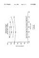
- FIG. 1is a schematic of the use of the present invention
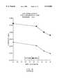
- FIG. 2is a graph of linewidth in nanometers (nm) plotted against focus in microns ( ⁇ m) of a formulation of a standard negative resist at various exposure energies;
- FIG. 3is a graph of linewidth for a negative tone line of a hybrid pattern in nm plotted against focus in ⁇ m of a hybrid resist of the present invention at various exposure energies;
- FIG. 4is a graph showing the linewidth in nm plotted against the amount of positive tone solubility inhibitor (MOP) incorporated in a hybrid resist of the present invention
- FIG. 5is a comparative model of what the range of focus is for a given linewidth using standard resist formulations and a hybrid resist formulation of the present invention
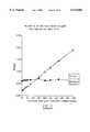
- FIG. 6is a graph showing the relationship between the cell area and the generation of the device.
- FIG. 7is a color schematic showing a sample layout for a six square cell in which a hybrid resist of the present invention may be used to form the bitline;
- FIG. 8is a color schematic showing a sample layout for a four square cell in which a hybrid resist of the present invention may be used to form the device;
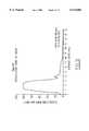
- FIG. 9is a graph showing the dissolution rate in nanometers per second (nm/sec) as a function of the exposure dose in millijoules (mJ) using one formulation of a hybrid resist of the present;
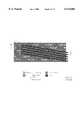
- FIG. 10is a scanning electron micrograph of the lines and spaces formed using one formulation of a hybrid resist of the present invention.
- FIG. 11is a graph showing the resultant line and space widths as functions of the chrome space width using one formulation of a hybrid resist of the present invention.
- FIG. 12is a graph showing the dissolution rate of an alternative formulation of the hybrid resist in nm/sec as a function of the exposure dose in mJ;
- FIG. 13is a graph showing the variation in space width in ⁇ m as a function of MOP loading using one formulation of hybrid resist of the present invention
- FIG. 14is a graph of the response of a formulation of the hybrid resist of the present invention in which exposed (negative) line, unexposed (positive) line and space widths are plotted as a function of exposure dose;
- FIG. 15is a scanning electron micrograph of 0.18 ⁇ m resist lines and spaces printed on a 0.5 numerical aperture (NA) deep ultra violet (DUV) expose tool with a hybrid resist formulation as described in Example 2 of the present invention.
- NAnumerical aperture
- DUVdeep ultra violet
- the present inventionprovides a photoresist material having, simultaneously, both a positive tone and a negative tone response to exposure.
- the positive tone responsedominates at the lower exposure dose while the negative response predominates at the higher exposure dosages. Exposure of this resist creates a space/line/space combination, whereas either of the conventional resists would produce only a single feature.
- FIG. 16a graph is illustrated showing how the positive resist undergoes an increase in solubility as the exposure dose is increased.
- FIG. 19the line pattern for negative resist printed with a reticle line pattern is illustrated.
- the positive tone responsecauses an increase in solubility in the areas where diffraction effects have reduced the expose intensity, such as the areas near the edge of the reticle image.
- the negative tone responsepredominates, causing a reduction in solubility in the more highly exposed areas.
- FIG. 20the graph of the resist solubility as a function of exposure dose for hybrid resist is illustrated.
- Printing a reticle line pattern onto a substrateresults in the space/line/space pattern illustrated in FIG. 21.
- FIG. 1illustrates these salient differences between a positive resist, a negative resist, and a hybrid resist.
- the frequency doubling hybrid resistis typically formulated using components of existing positive and negative tone resists. This includes, for example, poly(hydroxystyrene) resins which are partially modified with acid-sensitive solubility dissolution inhibiting functionalities, a cross-linker, a photo-acid generator, and, optionally, a base additive and a photosensitizer.
- the resist formulationsmay be varied to obtain a fast positive tone reaction and a slow negative tone reaction for optimal results.
- the positive tone componentcan be chosen such that it is relatively insensitive to post expose bake temperatures, while the negative tone portion is chosen to be more highly sensitive to post expose bake temperatures. In this way, the relative sensitivity of the positive and negative responses can be altered with bake temperatures to provide the desired imaging results.
- the resist formulationsmay be altered to provide space widths of different dimensions. For example, as the amount of solubility inhibitor on the poly(hydroxystyrene) resin is increased, the printed space width becomes smaller (FIG. 13). This approach may also be used to alter the isofocal print bias of the negative tone line; at higher positive tone solubility inhibitor concentrations, the isofocal print bias of the negative tone line increases (FIG. 4). This is desirable in some applications for reducing the size of the printed negative tone line, optimizing the frequency doubling characteristics of the resist.
- the relative responses of the positive and negative tone functions of the hybrid resistcan also be altered by modifying the exposure conditions.
- the negative tone line of the hybrid resistdoes vary with exposure dose and reticle dimension, similar to the behavior of a conventional resist.
- the negative tone lineincreases in width, and the spaces remain the same size, but the spaces are shifted to a new position on the substrate, since they lie adjacent to the negative line.
- the positive tone linesalter in size as the exposure dose or reticle dimension are altered.
- two reticlescould be used to print two separate patterns in the resist.
- One reticlecould be exposed with a high dose, causing the hybrid functions to be expressed in the resist.
- Another reticlecould be exposed in the same resist film at a lower dose, causing only the positive tone function to be expressed in that portion of the resist.
- This effectcould also be accomplished with a single expose process if, for example, the reticle contained a partial filter of the actinic radiation in the areas where a lower exposure dose was desired. This allows wider spaces to be printed at the same time as the narrower features, which is necessary in some device applications.
- a hybrid resistcan be used to create a standard negative tone pattern. If the resist film is image-wise exposed with a standard negative tone reticle, baked to form the hybrid image, then blanket exposed with actinic radiation and developed without a second post-expose bake process, the result is a standard negative tone image.
- This approachmay be desirable in some applications, such as the formation of gate conductor circuits, which require very small lines to be printed, but do not require a high density image pitch.
- the resistmay be blanket exposed to a low dose of actinic energy after the image-wise exposure and before the baking step. The desirability of the method would depend on whether a solubility inhibiting protective group is present on the resin and whether the positive tone response is temperature dependent.
- the negative tone line of the hybrid resistcan exhibit a large print bias at its isofocal point, as shown in FIG. 3.
- the resist image sizecan be substantially smaller than the reticle image size. This is desirable because the aerial image is less degraded by diffraction effects at the larger reticle size, thus allowing a larger depth of focus to be attained than is possible with conventional positive and negative tone systems, as shown in FIG. 2.
- This print biasis a result of the fact that the edge of the chrome line prints as a space. The space, in effect, acts to ⁇ trim ⁇ the edges of the aerial image, causing the negative line to print smaller than it would with a conventional negative resist. This is an expression of the frequency doubling character of a hybrid resist.
- the resist formulationit is possible to design the resist formulation to optimize the print bias of the negative tone line. For example, by choosing an appropriate loading factor for the positive tone solubility inhibitor, one may obtain a particular print bias as shown in FIG. 4. In theory, it is quite obvious that similar variations in the photoresist response can also be brought about by making appropriate changes in concentrations and reactivities of other components as well.
- the isofocal print bias for a hybrid resistcan be 0.11 ⁇ m larger than the isofocal print bias for a standard negative tone resist, as exemplified in FIGS. 2 and 3 when standard calculations known in the art are performed on the data.
- This differencecan be utilized in two ways. In one approach, the same reticle image size could be used with the hybrid resist to print a smaller line than the standard resist, while maintaining focus and exposure process latitude. In another manner of use, the size of the reticle features could be increased with the hybrid resist relative to the standard resist, while printing the same image size as the standard resist.
- the resist formulationsmay be varied to obtain a high photospeed positive tone reaction and a low photospeed negative tone reaction for optimal results.
- the positive tone resistmay be chosen so that it is insensitive to post expose bake (PEB) conditions so that the ratio of sensitivity of the positive tone to the negative tone function can be altered, thus changing the ratios of the space/line/space combinations.
- PEBpost expose bake
- a gray-scale filterin the reticle of the exposure tool.
- a gray scale filteronly allows a portion of the radiation to pass through the reticle, thereby creating areas of intermediate exposure. This prevents the negative tone resist function from operating in these areas because the exposure dose would never reach the critical point, but would still allow the positive functions to occur, thereby creating wider spaces. This allows wider spaces to be printed at the same time as the narrower features, which is necessary in some device applications.
- the doughnut shaped features that are typically obtainedcan be trimmed with a second masking step if they are not desired.
- circular or oblong doughnut-shaped trenchesare desirable in deep trench capacitors in dynamic random access memory (DRAM) and first level wiring of the 1 gigabyte(GB) DRAM, lines are necessary for the four square (4 SQ) and six square (6 SQ) wiring of bitlines and wordlines.
- FIG. 6the trends in cell area per generation show that the typical eight square (8 SQ) line is not going to meet the area requirements for the 1 GB and higher density devices. For this reason, changes in device layout, such as staggered bitlines, have been suggested.
- the reliable, sub-lithographic features, as disclosed in the present inventionthe folded bitline architecture of the chip would still be possible. Additionally, should further advances be made in the device layout, the ability to reduce the feature size may enhance the device's overall performance and size.
- a 6 SQ stacked capacitor folded bitline architectureis provided in which the pitch of the bitline is 1.5 F, as is required in order to make the appropriate connections.
- a 4 SQ stacked capacitor folded bitline architectureis attainable with the current technology as shown in FIG. 8.
- the stacked capacitors in the y-directionwill also have to be defined using the hybrid resist of the present invention.
- the photoresist resins suitable for use in accordance with the inventioninclude any of the base-soluble, long chain polymers suitable for use as a polymer resin in a photoresist formulation.
- Specific examplesinclude: (i) aromatic polymers having an --OH group, e.g., polyhydroxystyrenes such as poly (4-hydroxystyrene), poly (3-hydroxystyrene), commercially available from Hoechst Celanese of Corpus Christi, Tex., novolak resins commercially available from Shipley of Marlboro, Mass., and polymers having a phenolic --OH group, e.g., phenol formaldehyde resins; (ii) polymers having an acid group, e.g., polymethacrylic acid with an ester side chain; and (iii) acrylamide group type polymers.
- aromatic polymers having an --OH groupe.g., polyhydroxystyrenes such as poly (4-hydroxystyrene), poly (3-hydroxysty
- the polymer resin in its deprotected formi.e., once the positive tone reaction has occurred, is base soluble and compatible with developer solutions, such as aqueous solutions of metal-free ammonium hydroxide, tetramethylammonium hydroxide, and tetraethyl ammonium hydroxide, metal containing potassium hydroxide, and sodium metasilicate.
- developer solutionssuch as aqueous solutions of metal-free ammonium hydroxide, tetramethylammonium hydroxide, and tetraethyl ammonium hydroxide, metal containing potassium hydroxide, and sodium metasilicate.
- Preferred polymer resinshave an average molecular weight within the range of about 1,000 daltons to about 250,000 daltons, and most preferably within the range of about 1,000 to 25,000 daltons, to enhance its solubility in developer solutions.
- Examplesinclude p-hydroxystyrene-maleic acid anhydride copolymers, polyhydroxystyrene-p-tertiarybutylcarganatostyrene co-polymers, poly(2-hydroxystyrene), phenolformaldehyde resins, polymethyl methacrylate-tertiary butyl methacrylate-polymethacrylic acid terpolymers, poly-4-hydroxystyrene-tertiary butyl methacrylate copolymers, poly(4-hydroxystyrene) with one or more acid labile alkyl or aryl substituents on the aromatic ring, a poly(3-hydroxystyrene) with one or more alkyl or aryl substituents on the aromatic ring, or any of these as the major number of subunits in a copolymer, such as PHM-C, commercially available from Maruzen America of New York, N.Y.
- the PHM-Cincludes both poly (hydroxystyrene) subunits and vinyl cyclohexanol subunits preferably being in the range of about 99:1 to about 50:50.
- the most preferred ratiois about 90 poly (hydroxystyrene) units to about 10 vinyl cyclohexanol subunits.
- Crosslinking compositionsare preferably tetramethoxymethyl glycouril ("Powderlink”) and 2,6-bis(hydroxymethyl)-p-cresol.
- other possible crosslinking compositionsinclude: ##STR1## their analogs and derivatives, as can be found in Japanese Laid-Open Patent Application (Kokai) No. 1-293339, as well as etherified amino resins, for example methylated or butylated melamine resins (N-methoxymethyl- or N-butoxymethyl-melamine respectively) or methylated/butylated glycol-urils, for example of the formula: ##STR2## as can be found in Canadian Patent No. 1 204 547.
- Photoacid generatorsinclude, but are not limited to: N-(trifluoromethylsulfonyloxy)-bicyclo[2.2.1]hept-5-ene-2,3-dicarboximide (“MDT”), onium salts, aromatic diazonium salts, sulfonium salts, diaryliodonium salts and sulfonic acid esters of N-hydroxyamides or -imides, as disclosed in U.S. Pat. No. 4,731,605, incorporated herein by reference. Also, a PAG that produces a weaker acid such as dodecane sulfonate of N-hydroxynaphthalimide (“DDSN”) may be used.
- DDSNdodecane sulfonate of N-hydroxynaphthalimide
- Possible base additivesinclude, but are not limited to: dimethylamino pyridine, 7-diethylamino-4-methyl coumarin ("Coumarin 1"), tertiary amines, proton sponge, berberine, and the polymeric amines as in the "Pluronic” or “Tetronic” series from BASF. Additionally, tetra alkyl ammonium hydroxides or cetyltrimethyl ammonium hydroxide, may be used when the PAG is an onium salt.
- sensitizersexamples include: chrysenes, pyrenes, fluoranthenes, anthrones, benzophenones, thioxanthones, and anthracenes, such as 9-anthracene methanol (9-AM). Additional anthracene derivative sensitizers are disclosed in U.S. Pat. No. 4,371,605, which is incorporated herein by reference.
- the sensitizermay include oxygen or sulfur.
- the preferred sensitizerswill be nitrogen free, because the presence of nitrogen, e.g., an amine or phenothiazine group, tends to sequester the free acid generated during the exposure process and the formulation will lose photosensitivity.
- Sample casting solventis used to provide proper consistency to the entire composition so that it may be applied to the substrate surface without the layer being too thick or too thin.
- Sample casting solventsinclude: ethoxyethylpropionate (“EEP”), a combination of EEP and ⁇ -butyrolactone (“GBL”), and propyleneglycolmonoethylether acetate (PM acetate).
- the basis of the inventionlies in the fact that the hybrid resist is comprised of a negative tone component and a positive tone component, wherein the positive tone component acts at a first actinic energy level and the negative tone component acts at a second actinic energy level, the first and second actinic energy levels being separated by an intermediate range of actinic energy levels.
- compositionswere dissolved in propyleneglycol monomethylether acetate (PM acetate) solvent available from Pacific Pac, Inc., Hollister, Calif. containing 350 ppm of FC-430, a non-ionic fluorinated alkyl ester surfactant available from 3M, St. Paul, Minn. for a total of 20% solids:
- PM acetatepropyleneglycol monomethylether acetate
- PHSpoly(hydroxystyrene)
- MOPmethoxypropene
- the solutionwas filtered through a 0.2 ⁇ m filter.
- the solutionwas coated onto silicon wafers primed with hexamethyl-disilazane with a soft bake of 110° Celsius (C.) resulting in films of about 0.8 ⁇ m thick as determined by a Nanospec reflectance spectrophotometer.
- the coated waferswere then exposed with deep ultraviolet (DUV) excimer laser radiation having a wavelength of 248 nm in a 0.37 numerical aperture (NA) Canon stepper with a matrix of different doses from low doses to high doses and post expose baked (PEB) at 110° C. for 90 sec.
- DUVdeep ultraviolet
- NAnumerical aperture
- the dissolution rates of the exposed filmswere calculated from the thickness of remaining film after developing for a given amount of time with 0.14 Normal (N) tetramethylammonium hydroxide (TMAH) developer.
- the dissolution rate vs. exposure dose relationshipis shown in FIG. 9.
- the resisthas a very low dissolution rate (about 2 nm/sec) when unexposed.
- the dissolution rateincreases until reaching about 50 nm/sec.
- the dissolution rateremains relatively constant at this level in the dose range of about 1 millijoule (mJ) to about 3 mJ.
- mJmillijoule
- the negative cross-linking chemistrybecomes predominant and the dissolution rate falls back to a value close to zero.
- FIG. 10shows the outcome of exposing the resist through a mask having 1 ⁇ m wide nested chrome lines at a pitch of 2 m with a 248 DUV stepper with a 0.37 NA. Every chrome line and space combination in the mask prints as two lines and two spaces on the resist: a negative line of about 0.8 ⁇ m, a positive tone line of about 0.6 ⁇ m and two equal spaces of about 0.3 ⁇ m.
- This exampleillustrates the manner in which changing the type of photoacid generator and relative amounts of the various components can change the dissolution rate characteristics of the hybrid resist and subsequently the lithographic response.
- This second formulationwas prepared and processed in a manner similar to EXAMPLE 1, however, it is comprised of the following components:
- triphenyl sulfonium triflate1.3% of solids
- the dissolution rate characteristic of the resulting hybrid resistis shown in FIG. 12.
- the overall nature of the curveremains similar to that shown by the hybrid resist of EXAMPLE 1, in that the dissolution rate starts out low for an unexposed resist, increases to a high at about 5 mJ and decreases to a low above 7 mJ.
- the absolute dose range and the dissolution rates within these rangesare quite different from those shown in FIG. 9.
- FIG. 14represents the response of this formulation of the hybrid resist when exposed through a mask of nested chrome lines and spaces of equal widths in a MICRASCAN II DUV 0.5 NA stepper tool. Negative line, unexposed (positive) line and space widths are plotted as a function of mask dimension. The space remains relatively constant in the range of about 0.18 ⁇ m, whereas both lines vary as the mask dimension is varied. Resist images representative of this formulation and process are shown in FIG. 15.
- This exampleillustrates that the space width of the frequency doubled image can be changed by varying the protection level of PHS with MOP.
- Negative tone imagingmay be performed with the hybrid resist of the present invention, using a blanket DUV expose after the PEB and prior to the develop.
- the initial image-wise expose dosewas 17-24 mJ/cm2, the post expose bake temperature was 110° C. for 90 sec and the develop time was 100 sec in 0.14 N TMAH.
- a standard negative tone resistwas processed in a similar fashion, with the omission of a blanket expose step as a control.
- the electrical data from this experimentis shown in FIGS. 2 and 3.
- a large isofocal print bias of approximately 0.11 ⁇ mwas observed for the hybrid resist relative to the standard negative resist, as calculated using standard methods known in the art.
Landscapes
- Physics & Mathematics (AREA)
- Engineering & Computer Science (AREA)
- General Physics & Mathematics (AREA)
- Microelectronics & Electronic Packaging (AREA)
- Manufacturing & Machinery (AREA)
- Computer Hardware Design (AREA)
- Condensed Matter Physics & Semiconductors (AREA)
- Power Engineering (AREA)
- Spectroscopy & Molecular Physics (AREA)
- Architecture (AREA)
- Structural Engineering (AREA)
- Exposure And Positioning Against Photoresist Photosensitive Materials (AREA)
- Materials For Photolithography (AREA)
Abstract
Description
Claims (21)
Priority Applications (12)
| Application Number | Priority Date | Filing Date | Title |
|---|---|---|---|
| US08/715,287US6114082A (en) | 1996-09-16 | 1996-09-16 | Frequency doubling hybrid photoresist having negative and positive tone components and method of preparing the same |
| US08/790,876US5776660A (en) | 1996-09-16 | 1997-02-03 | Fabrication method for high-capacitance storage node structures |
| KR1019970023549AKR100268292B1 (en) | 1996-09-16 | 1997-06-09 | Frequency doubling hybrid resist |
| US08/878,136US6391426B1 (en) | 1996-09-16 | 1997-06-19 | High capacitance storage node structures |
| JP22504197AJP3723670B2 (en) | 1996-09-16 | 1997-08-21 | Frequency double hybrid photo resist |
| KR1019970047397AKR100293401B1 (en) | 1996-09-16 | 1997-09-13 | Fabrication method for high-capacitance storage node structures |
| TW086113401ATW463227B (en) | 1996-09-16 | 1997-09-15 | Frequency doubling hybrid photoresist |
| JP25115797AJP4233621B2 (en) | 1996-09-16 | 1997-09-16 | Method for manufacturing a high capacitance storage node structure in a substrate, and substrate having a high capacitance storage node |
| US09/021,924US6372412B1 (en) | 1996-09-16 | 1998-02-10 | Method of producing an integrated circuit chip using frequency doubling hybrid photoresist and apparatus formed thereby |
| US09/110,487US6313492B1 (en) | 1996-09-16 | 1998-07-06 | Integrated circuit chip produced by using frequency doubling hybrid photoresist |
| US09/170,756US6200726B1 (en) | 1996-09-16 | 1998-10-13 | Optimization of space width for hybrid photoresist |
| JP2008199617AJP5042160B2 (en) | 1996-09-16 | 2008-08-01 | Method for manufacturing a high capacitance storage node structure in a substrate, and substrate having a high capacitance storage node |
Applications Claiming Priority (1)
| Application Number | Priority Date | Filing Date | Title |
|---|---|---|---|
| US08/715,287US6114082A (en) | 1996-09-16 | 1996-09-16 | Frequency doubling hybrid photoresist having negative and positive tone components and method of preparing the same |
Related Child Applications (4)
| Application Number | Title | Priority Date | Filing Date |
|---|---|---|---|
| US08/790,876Continuation-In-PartUS5776660A (en) | 1996-09-16 | 1997-02-03 | Fabrication method for high-capacitance storage node structures |
| US09/021,924DivisionUS6372412B1 (en) | 1996-09-16 | 1998-02-10 | Method of producing an integrated circuit chip using frequency doubling hybrid photoresist and apparatus formed thereby |
| US09/110,487DivisionUS6313492B1 (en) | 1996-09-16 | 1998-07-06 | Integrated circuit chip produced by using frequency doubling hybrid photoresist |
| US09/170,756Continuation-In-PartUS6200726B1 (en) | 1996-09-16 | 1998-10-13 | Optimization of space width for hybrid photoresist |
Publications (1)
| Publication Number | Publication Date |
|---|---|
| US6114082Atrue US6114082A (en) | 2000-09-05 |
Family
ID=24873424
Family Applications (3)
| Application Number | Title | Priority Date | Filing Date |
|---|---|---|---|
| US08/715,287Expired - LifetimeUS6114082A (en) | 1996-09-16 | 1996-09-16 | Frequency doubling hybrid photoresist having negative and positive tone components and method of preparing the same |
| US09/021,924Expired - Fee RelatedUS6372412B1 (en) | 1996-09-16 | 1998-02-10 | Method of producing an integrated circuit chip using frequency doubling hybrid photoresist and apparatus formed thereby |
| US09/110,487Expired - Fee RelatedUS6313492B1 (en) | 1996-09-16 | 1998-07-06 | Integrated circuit chip produced by using frequency doubling hybrid photoresist |
Family Applications After (2)
| Application Number | Title | Priority Date | Filing Date |
|---|---|---|---|
| US09/021,924Expired - Fee RelatedUS6372412B1 (en) | 1996-09-16 | 1998-02-10 | Method of producing an integrated circuit chip using frequency doubling hybrid photoresist and apparatus formed thereby |
| US09/110,487Expired - Fee RelatedUS6313492B1 (en) | 1996-09-16 | 1998-07-06 | Integrated circuit chip produced by using frequency doubling hybrid photoresist |
Country Status (4)
| Country | Link |
|---|---|
| US (3) | US6114082A (en) |
| JP (1) | JP3723670B2 (en) |
| KR (2) | KR100268292B1 (en) |
| TW (1) | TW463227B (en) |
Cited By (45)
| Publication number | Priority date | Publication date | Assignee | Title |
|---|---|---|---|---|
| US6358793B1 (en)* | 1999-02-26 | 2002-03-19 | Micron Technology, Inc. | Method for localized masking for semiconductor structure development |
| US6387783B1 (en)* | 1999-04-26 | 2002-05-14 | International Business Machines Corporation | Methods of T-gate fabrication using a hybrid resist |
| US6461800B1 (en)* | 1999-09-29 | 2002-10-08 | Mitsubishi Denki Kabushiki Kaisha | Resist patterning method |
| US6627361B2 (en) | 2001-07-09 | 2003-09-30 | International Business Machines Corporation | Assist features for contact hole mask patterns |
| US20040033441A1 (en)* | 2002-08-19 | 2004-02-19 | Fuji Photo Film Co., Ltd. | Negative resist composition |
| US20050202613A1 (en)* | 2004-01-29 | 2005-09-15 | Rohm And Haas Electronic Materials Llc | T-gate formation |
| US20060060562A1 (en)* | 2004-09-20 | 2006-03-23 | International Business Machines Corporation | Sub-lithographic imaging techniques and processes |
| US7192910B2 (en) | 2003-10-28 | 2007-03-20 | Sachem, Inc. | Cleaning solutions and etchants and methods for using same |
| US20080020325A1 (en)* | 2006-07-21 | 2008-01-24 | National Taiwan University | Positive and negative dual function magnetic resist lithography |
| US20080113157A1 (en)* | 2006-11-13 | 2008-05-15 | Seagate Technology Llc | Method for fabricating master stamper/imprinters for patterned recording media utilizing hybrid resist |
| EP1959298A2 (en) | 2007-02-16 | 2008-08-20 | Forschungszentrum Karlsruhe GmbH | Method for structuring a layer onto a substrate |
| US20090068589A1 (en)* | 2007-09-06 | 2009-03-12 | Massachusetts Institute Of Technology | Multi-tone resist compositions |
| US20090130611A1 (en)* | 2005-09-06 | 2009-05-21 | Nxp B.V. | Lithographic Method |
| WO2010033720A1 (en)* | 2008-09-19 | 2010-03-25 | Tokyo Electron Limited | Dual tone development processes |
| US20110091812A1 (en)* | 2009-10-16 | 2011-04-21 | Shin-Etsu Chemical Co., Ltd. | Patterning process and resist composition |
| US20110102528A1 (en)* | 2009-10-30 | 2011-05-05 | Fujifilm Corporation | Composition, resist film, pattern forming method, and inkjet recording method |
| US20120148957A1 (en)* | 2009-10-06 | 2012-06-14 | Fujifilm Corporation | Pattern forming method, chemical amplification resist composition and resist film |
| US8232198B2 (en) | 2010-08-05 | 2012-07-31 | International Business Machines Corporation | Self-aligned permanent on-chip interconnect structure formed by pitch splitting |
| US20120202349A1 (en)* | 2009-03-31 | 2012-08-09 | Sam Xunyun Sun | Photo-imageable Hardmask with Dual Tones for Microphotolithography |
| CN103376660A (en)* | 2012-04-27 | 2013-10-30 | 国际商业机器公司 | Photoresist composition containing a protected hydroxyl group for negative development and pattern forming method using thereof |
| US8580479B2 (en) | 2010-11-03 | 2013-11-12 | Empire Technology Development, Llc | Lithography using photoresist with photoinitiator and photoinhibitor |
| US20140242502A1 (en)* | 2011-11-10 | 2014-08-28 | Fujifilm Corporation | Actinic-ray- or radiation-sensitive resin composition, actinic-ray- or radiation-sensitive film, mask blank and method of forming pattern |
| US8822137B2 (en) | 2011-08-03 | 2014-09-02 | International Business Machines Corporation | Self-aligned fine pitch permanent on-chip interconnect structures and method of fabrication |
| US8828647B2 (en) | 2011-05-30 | 2014-09-09 | Shin-Etsu Chemical Co., Ltd. | Patterning process and resist composition |
| US8856697B2 (en) | 2011-02-23 | 2014-10-07 | Synopsys, Inc. | Routing analysis with double pattern lithography |
| TWI459438B (en)* | 2008-09-17 | 2014-11-01 | Tokyo Electron Ltd | Dual tone development processes |
| TWI459440B (en)* | 2009-04-27 | 2014-11-01 | Tokyo Electron Ltd | Flood exposure process for dual tone development in lithographic applications |
| US8890318B2 (en) | 2011-04-15 | 2014-11-18 | International Business Machines Corporation | Middle of line structures |
| US8900988B2 (en) | 2011-04-15 | 2014-12-02 | International Business Machines Corporation | Method for forming self-aligned airgap interconnect structures |
| US8932796B2 (en) | 2011-11-10 | 2015-01-13 | International Business Machines Corporation | Hybrid photoresist composition and pattern forming method using thereof |
| US9041116B2 (en) | 2012-05-23 | 2015-05-26 | International Business Machines Corporation | Structure and method to modulate threshold voltage for high-K metal gate field effect transistors (FETs) |
| US9054160B2 (en) | 2011-04-15 | 2015-06-09 | International Business Machines Corporation | Interconnect structure and method for fabricating on-chip interconnect structures by image reversal |
| US9086623B2 (en) | 2011-08-30 | 2015-07-21 | Fujifilm Corporation | Method of forming pattern, actinic-ray- or radiation-sensitive resin composition and actinic-ray- or radiation-sensitive film |
| US20150241773A1 (en)* | 2014-02-24 | 2015-08-27 | Alex Philip Graham Robinson | Two-Step Photoresist Compositions and Methods |
| US9236298B2 (en) | 2011-09-08 | 2016-01-12 | Globalfoundries Inc. | Methods for fabrication interconnect structures with functional components and electrical conductive contact structures on a same level |
| US9299847B2 (en) | 2012-05-10 | 2016-03-29 | Globalfoundries Inc. | Printed transistor and fabrication method |
| US9366963B2 (en) | 2013-11-28 | 2016-06-14 | Shin-Etsu Chemical Co., Ltd. | Resist composition and pattern forming process |
| US20160209747A1 (en)* | 2013-09-26 | 2016-07-21 | Fujifilm Corporation | Active light sensitive or radiation sensitive composition, and resist film, pattern forming method, resist-coated mask blank, method for producing photomask, photomask, method for manufacturing electronic device, and electronic device, each of which uses said active light sensitive or radiation sensitive composition |
| US9599895B2 (en) | 2011-04-12 | 2017-03-21 | Empire Technology Development Llc | Lithography using photoresist with photoinitiator and photoinhibitor |
| US9678435B1 (en)* | 2014-09-22 | 2017-06-13 | Mentor Graphics, A Siemens Business | Horizontal development bias in negative tone development of photoresist |
| TWI621159B (en)* | 2013-11-22 | 2018-04-11 | 格芯公司 | Structure and method for forming N-type and P-type complementary MOS field-effect transistors with different channel materials |
| WO2020014026A1 (en)* | 2018-07-09 | 2020-01-16 | Applied Materials, Inc. | Photoresist composition for line doubling |
| WO2020092963A1 (en)* | 2018-11-02 | 2020-05-07 | Brewer Science, Inc. | Bottom-up conformal coating and photopatterning on pag-immobilized surfaces |
| US10799613B2 (en) | 2013-10-30 | 2020-10-13 | California Institute Of Technology | Direct photopatterning of robust and diverse materials |
| US11592740B2 (en)* | 2017-05-16 | 2023-02-28 | Applied Materials, Inc. | Wire grid polarizer manufacturing methods using frequency doubling interference lithography |
Families Citing this family (13)
| Publication number | Priority date | Publication date | Assignee | Title |
|---|---|---|---|---|
| KR100328824B1 (en)* | 1999-07-09 | 2002-03-14 | 박종섭 | Manufacturing method for capacitor |
| US6495435B2 (en)* | 2000-02-17 | 2002-12-17 | Advance Micro Devices, Inc. | Method for improved control of lines adjacent to a select gate using a mask assist feature |
| US7049246B1 (en)* | 2000-05-19 | 2006-05-23 | Newport Fab, Llc | Method for selective fabrication of high capacitance density areas in a low dielectric constant material |
| KR100433847B1 (en)* | 2001-12-15 | 2004-06-04 | 주식회사 하이닉스반도체 | Method for forming of storagenode |
| US6905811B2 (en)* | 2003-04-22 | 2005-06-14 | Headway Technologies, Inc. | Method to form reduced dimension pattern with good edge roughness |
| US6780736B1 (en)* | 2003-06-20 | 2004-08-24 | International Business Machines Corporation | Method for image reversal of implant resist using a single photolithography exposure and structures formed thereby |
| US7897323B2 (en)* | 2004-11-25 | 2011-03-01 | Nxp B.V. | Lithographic method |
| US7387916B2 (en)* | 2004-12-02 | 2008-06-17 | Texas Instruments Incorporated | Sharp corner lead frame |
| US7358140B2 (en)* | 2005-11-04 | 2008-04-15 | International Business Machines Corporation | Pattern density control using edge printing processes |
| JP5277203B2 (en)* | 2006-12-25 | 2013-08-28 | 富士フイルム株式会社 | PATTERN FORMATION METHOD, POSITIVE RESIST COMPOSITION FOR MULTIPLE DEVELOPMENT USED FOR THE PATTERN FORMATION METHOD, NEGATIVE DEVELOPMENT SOLUTION USED FOR THE PATTERN FORMATION METHOD, AND NEGATIVE DEVELOPMENT RINS |
| JP5556452B2 (en)* | 2010-07-06 | 2014-07-23 | 信越化学工業株式会社 | Pattern formation method |
| JP5556451B2 (en)* | 2010-07-06 | 2014-07-23 | 信越化学工業株式会社 | Pattern formation method |
| KR20130039124A (en)* | 2011-10-11 | 2013-04-19 | 삼성전자주식회사 | Method for forming patterns of semiconductor device |
Citations (12)
| Publication number | Priority date | Publication date | Assignee | Title |
|---|---|---|---|---|
| US4405708A (en)* | 1981-03-12 | 1983-09-20 | U.S. Philips Corporation | Method of applying a resist pattern on a substrate, and resist material mixture |
| US4568631A (en)* | 1984-04-30 | 1986-02-04 | International Business Machines Corporation | Process for delineating photoresist lines at pattern edges only using image reversal composition with diazoquinone |
| US4687730A (en)* | 1985-10-30 | 1987-08-18 | Rca Corporation | Lift-off technique for producing metal pattern using single photoresist processing and oblique angle metal deposition |
| US4707218A (en)* | 1986-10-28 | 1987-11-17 | International Business Machines Corporation | Lithographic image size reduction |
| US4889789A (en)* | 1987-04-03 | 1989-12-26 | Hoechst Aktiengsellschaft | Photosensitive composition and photosensitive copying material prepared therefrom wherein composition has a thermal crosslinking urethane formaldehyde condensate |
| US5070001A (en)* | 1986-11-05 | 1991-12-03 | Hoechst Aktiengesellschaft | Light-sensitive mixture for producing positive or negative relief copies |
| JPH05297597A (en)* | 1992-04-23 | 1993-11-12 | Fujitsu Ltd | Method of forming resist pattern |
| US5330879A (en)* | 1992-07-16 | 1994-07-19 | Micron Technology, Inc. | Method for fabrication of close-tolerance lines and sharp emission tips on a semiconductor wafer |
| US5338626A (en)* | 1991-11-22 | 1994-08-16 | At&T Bell Laboratories | Fabrication of phase-shifting lithographic masks |
| US5585218A (en)* | 1993-06-02 | 1996-12-17 | Sumitomo Chemical Company, Limited | Photoresist composition containing alkyletherified polyvinylphenol |
| US5629135A (en)* | 1993-07-15 | 1997-05-13 | Japan Synthetic Rubber Co., Ltd. | Chemically amplified resist composition |
| US5648196A (en)* | 1995-07-14 | 1997-07-15 | Cornell Research Foundation, Inc. | Water-soluble photoinitiators |
Family Cites Families (4)
| Publication number | Priority date | Publication date | Assignee | Title |
|---|---|---|---|---|
| JPH0682800B2 (en)* | 1985-04-16 | 1994-10-19 | 株式会社東芝 | Semiconductor memory device |
| US5210000A (en)* | 1989-05-22 | 1993-05-11 | Shipley Company Inc. | Photoresist and method for forming a relief image utilizing composition with copolymer binder having a major proportion of phenolic units and a minor proportion of non-aromatic cyclic alcoholic units |
| US5296332A (en)* | 1991-11-22 | 1994-03-22 | International Business Machines Corporation | Crosslinkable aqueous developable photoresist compositions and method for use thereof |
| JP3037509B2 (en)* | 1992-08-04 | 2000-04-24 | 新日本製鐵株式会社 | Method for manufacturing semiconductor memory device |
- 1996
- 1996-09-16USUS08/715,287patent/US6114082A/ennot_activeExpired - Lifetime
- 1997
- 1997-06-09KRKR1019970023549Apatent/KR100268292B1/ennot_activeExpired - Fee Related
- 1997-08-21JPJP22504197Apatent/JP3723670B2/ennot_activeExpired - Fee Related
- 1997-09-13KRKR1019970047397Apatent/KR100293401B1/ennot_activeExpired - Fee Related
- 1997-09-15TWTW086113401Apatent/TW463227B/ennot_activeIP Right Cessation
- 1998
- 1998-02-10USUS09/021,924patent/US6372412B1/ennot_activeExpired - Fee Related
- 1998-07-06USUS09/110,487patent/US6313492B1/ennot_activeExpired - Fee Related
Patent Citations (12)
| Publication number | Priority date | Publication date | Assignee | Title |
|---|---|---|---|---|
| US4405708A (en)* | 1981-03-12 | 1983-09-20 | U.S. Philips Corporation | Method of applying a resist pattern on a substrate, and resist material mixture |
| US4568631A (en)* | 1984-04-30 | 1986-02-04 | International Business Machines Corporation | Process for delineating photoresist lines at pattern edges only using image reversal composition with diazoquinone |
| US4687730A (en)* | 1985-10-30 | 1987-08-18 | Rca Corporation | Lift-off technique for producing metal pattern using single photoresist processing and oblique angle metal deposition |
| US4707218A (en)* | 1986-10-28 | 1987-11-17 | International Business Machines Corporation | Lithographic image size reduction |
| US5070001A (en)* | 1986-11-05 | 1991-12-03 | Hoechst Aktiengesellschaft | Light-sensitive mixture for producing positive or negative relief copies |
| US4889789A (en)* | 1987-04-03 | 1989-12-26 | Hoechst Aktiengsellschaft | Photosensitive composition and photosensitive copying material prepared therefrom wherein composition has a thermal crosslinking urethane formaldehyde condensate |
| US5338626A (en)* | 1991-11-22 | 1994-08-16 | At&T Bell Laboratories | Fabrication of phase-shifting lithographic masks |
| JPH05297597A (en)* | 1992-04-23 | 1993-11-12 | Fujitsu Ltd | Method of forming resist pattern |
| US5330879A (en)* | 1992-07-16 | 1994-07-19 | Micron Technology, Inc. | Method for fabrication of close-tolerance lines and sharp emission tips on a semiconductor wafer |
| US5585218A (en)* | 1993-06-02 | 1996-12-17 | Sumitomo Chemical Company, Limited | Photoresist composition containing alkyletherified polyvinylphenol |
| US5629135A (en)* | 1993-07-15 | 1997-05-13 | Japan Synthetic Rubber Co., Ltd. | Chemically amplified resist composition |
| US5648196A (en)* | 1995-07-14 | 1997-07-15 | Cornell Research Foundation, Inc. | Water-soluble photoinitiators |
Cited By (81)
| Publication number | Priority date | Publication date | Assignee | Title |
|---|---|---|---|---|
| US6358793B1 (en)* | 1999-02-26 | 2002-03-19 | Micron Technology, Inc. | Method for localized masking for semiconductor structure development |
| US6573554B2 (en) | 1999-02-26 | 2003-06-03 | Micron Technology, Inc. | Localized masking for semiconductor structure development |
| US7468534B2 (en) | 1999-02-26 | 2008-12-23 | Micron Technology, Inc. | Localized masking for semiconductor structure development |
| US20030205749A1 (en)* | 1999-02-26 | 2003-11-06 | Micron Technology, Inc. | Localized masking for semiconductor structure development |
| US20090102018A1 (en)* | 1999-02-26 | 2009-04-23 | Micron Technology, Inc. | Localized masking for semiconductor structure development |
| US7868369B2 (en) | 1999-02-26 | 2011-01-11 | Micron Technology, Inc. | Localized masking for semiconductor structure development |
| US20060006448A1 (en)* | 1999-02-26 | 2006-01-12 | Micron Technology, Inc. | Localized masking for semiconductor structure development |
| US7015529B2 (en) | 1999-02-26 | 2006-03-21 | Micron Technology, Inc. | Localized masking for semiconductor structure development |
| US6387783B1 (en)* | 1999-04-26 | 2002-05-14 | International Business Machines Corporation | Methods of T-gate fabrication using a hybrid resist |
| US6461800B1 (en)* | 1999-09-29 | 2002-10-08 | Mitsubishi Denki Kabushiki Kaisha | Resist patterning method |
| US6627361B2 (en) | 2001-07-09 | 2003-09-30 | International Business Machines Corporation | Assist features for contact hole mask patterns |
| US20040033441A1 (en)* | 2002-08-19 | 2004-02-19 | Fuji Photo Film Co., Ltd. | Negative resist composition |
| US7432034B2 (en)* | 2002-08-19 | 2008-10-07 | Fujifilm Corporation | Negative resist composition |
| US7192910B2 (en) | 2003-10-28 | 2007-03-20 | Sachem, Inc. | Cleaning solutions and etchants and methods for using same |
| US20060223245A9 (en)* | 2004-01-29 | 2006-10-05 | Rohm And Haas Electronic Materials Llc | T-gate formation |
| US20050202613A1 (en)* | 2004-01-29 | 2005-09-15 | Rohm And Haas Electronic Materials Llc | T-gate formation |
| US7413942B2 (en) | 2004-01-29 | 2008-08-19 | Rohm And Haas Electronic Materials Llc | T-gate formation |
| US20060060562A1 (en)* | 2004-09-20 | 2006-03-23 | International Business Machines Corporation | Sub-lithographic imaging techniques and processes |
| US7585614B2 (en) | 2004-09-20 | 2009-09-08 | International Business Machines Corporation | Sub-lithographic imaging techniques and processes |
| US7989155B2 (en) | 2005-09-06 | 2011-08-02 | Nxp B.V. | Lithographic method |
| US20090130611A1 (en)* | 2005-09-06 | 2009-05-21 | Nxp B.V. | Lithographic Method |
| US20080020325A1 (en)* | 2006-07-21 | 2008-01-24 | National Taiwan University | Positive and negative dual function magnetic resist lithography |
| US7598022B2 (en)* | 2006-07-21 | 2009-10-06 | National Taiwan University | Positive and negative dual function magnetic resist lithography |
| US20080113157A1 (en)* | 2006-11-13 | 2008-05-15 | Seagate Technology Llc | Method for fabricating master stamper/imprinters for patterned recording media utilizing hybrid resist |
| DE102007007719A1 (en)* | 2007-02-16 | 2008-08-21 | Forschungszentrum Karlsruhe Gmbh | Method for structuring a layer on a substrate |
| EP1959298A2 (en) | 2007-02-16 | 2008-08-20 | Forschungszentrum Karlsruhe GmbH | Method for structuring a layer onto a substrate |
| US20090068589A1 (en)* | 2007-09-06 | 2009-03-12 | Massachusetts Institute Of Technology | Multi-tone resist compositions |
| US8110339B2 (en) | 2007-09-06 | 2012-02-07 | Massachusetts Institute Of Technology | Multi-tone resist compositions |
| TWI459438B (en)* | 2008-09-17 | 2014-11-01 | Tokyo Electron Ltd | Dual tone development processes |
| WO2010033720A1 (en)* | 2008-09-19 | 2010-03-25 | Tokyo Electron Limited | Dual tone development processes |
| US8197996B2 (en) | 2008-09-19 | 2012-06-12 | Tokyo Electron Limited | Dual tone development processes |
| US20100119960A1 (en)* | 2008-09-19 | 2010-05-13 | Tokyo Electron Limited | Dual Tone Development Processes |
| US20120202349A1 (en)* | 2009-03-31 | 2012-08-09 | Sam Xunyun Sun | Photo-imageable Hardmask with Dual Tones for Microphotolithography |
| US8728710B2 (en)* | 2009-03-31 | 2014-05-20 | Sam Xunyun Sun | Photo-imageable hardmask with dual tones for microphotolithography |
| TWI459440B (en)* | 2009-04-27 | 2014-11-01 | Tokyo Electron Ltd | Flood exposure process for dual tone development in lithographic applications |
| US20120148957A1 (en)* | 2009-10-06 | 2012-06-14 | Fujifilm Corporation | Pattern forming method, chemical amplification resist composition and resist film |
| US8999621B2 (en)* | 2009-10-06 | 2015-04-07 | Fujifilm Corporation | Pattern forming method, chemical amplification resist composition and resist film |
| US20110091812A1 (en)* | 2009-10-16 | 2011-04-21 | Shin-Etsu Chemical Co., Ltd. | Patterning process and resist composition |
| US8507175B2 (en) | 2009-10-16 | 2013-08-13 | Shin-Etsu Chemical Co., Ltd. | Patterning process and resist composition |
| US20110102528A1 (en)* | 2009-10-30 | 2011-05-05 | Fujifilm Corporation | Composition, resist film, pattern forming method, and inkjet recording method |
| US8808961B2 (en)* | 2009-10-30 | 2014-08-19 | Fujifilm Corporation | Composition, resist film, pattern forming method, and inkjet recording method |
| US8795556B2 (en) | 2010-08-05 | 2014-08-05 | International Business Machines Corporation | Self-aligned permanent on-chip interconnect structure formed by pitch splitting |
| US8232198B2 (en) | 2010-08-05 | 2012-07-31 | International Business Machines Corporation | Self-aligned permanent on-chip interconnect structure formed by pitch splitting |
| US8580479B2 (en) | 2010-11-03 | 2013-11-12 | Empire Technology Development, Llc | Lithography using photoresist with photoinitiator and photoinhibitor |
| US8856697B2 (en) | 2011-02-23 | 2014-10-07 | Synopsys, Inc. | Routing analysis with double pattern lithography |
| US9599895B2 (en) | 2011-04-12 | 2017-03-21 | Empire Technology Development Llc | Lithography using photoresist with photoinitiator and photoinhibitor |
| US9490202B2 (en) | 2011-04-15 | 2016-11-08 | GlobalFoundries, Inc. | Self-aligned airgap interconnect structures |
| US9343354B2 (en) | 2011-04-15 | 2016-05-17 | Globalfoundries Inc. | Middle of line structures and methods for fabrication |
| US9245791B2 (en) | 2011-04-15 | 2016-01-26 | Globalfoundries Inc. | Method for fabricating a contact |
| US8890318B2 (en) | 2011-04-15 | 2014-11-18 | International Business Machines Corporation | Middle of line structures |
| US8900988B2 (en) | 2011-04-15 | 2014-12-02 | International Business Machines Corporation | Method for forming self-aligned airgap interconnect structures |
| US9054160B2 (en) | 2011-04-15 | 2015-06-09 | International Business Machines Corporation | Interconnect structure and method for fabricating on-chip interconnect structures by image reversal |
| US8828647B2 (en) | 2011-05-30 | 2014-09-09 | Shin-Etsu Chemical Co., Ltd. | Patterning process and resist composition |
| US9209126B2 (en) | 2011-08-03 | 2015-12-08 | Globalfoundries Inc. | Self-aligned fine pitch permanent on-chip interconnect structures and method of fabrication |
| US8822137B2 (en) | 2011-08-03 | 2014-09-02 | International Business Machines Corporation | Self-aligned fine pitch permanent on-chip interconnect structures and method of fabrication |
| US9086623B2 (en) | 2011-08-30 | 2015-07-21 | Fujifilm Corporation | Method of forming pattern, actinic-ray- or radiation-sensitive resin composition and actinic-ray- or radiation-sensitive film |
| US9236298B2 (en) | 2011-09-08 | 2016-01-12 | Globalfoundries Inc. | Methods for fabrication interconnect structures with functional components and electrical conductive contact structures on a same level |
| US8986918B2 (en) | 2011-11-10 | 2015-03-24 | International Business Machines Corporation | Hybrid photoresist composition and pattern forming method using thereof |
| US8932796B2 (en) | 2011-11-10 | 2015-01-13 | International Business Machines Corporation | Hybrid photoresist composition and pattern forming method using thereof |
| US9400430B2 (en)* | 2011-11-10 | 2016-07-26 | Fujifilm Corporation | Actinic-ray- or radiation-sensitive resin composition, actinic-ray- or radiation-sensitive film, mask blank and method of forming pattern |
| US20140242502A1 (en)* | 2011-11-10 | 2014-08-28 | Fujifilm Corporation | Actinic-ray- or radiation-sensitive resin composition, actinic-ray- or radiation-sensitive film, mask blank and method of forming pattern |
| US8846295B2 (en)* | 2012-04-27 | 2014-09-30 | International Business Machines Corporation | Photoresist composition containing a protected hydroxyl group for negative development and pattern forming method using thereof |
| CN103376660B (en)* | 2012-04-27 | 2017-12-05 | 国际商业机器公司 | Containing the photo-corrosion-resisting agent composition for protecting hydroxyl and its pattern formation method is used for negative development |
| CN103376660A (en)* | 2012-04-27 | 2013-10-30 | 国际商业机器公司 | Photoresist composition containing a protected hydroxyl group for negative development and pattern forming method using thereof |
| US20130288178A1 (en)* | 2012-04-27 | 2013-10-31 | International Business Machines Corporation | Photoresist composition containing a protected hydroxyl group for negative development and pattern forming method using thereof |
| US9299847B2 (en) | 2012-05-10 | 2016-03-29 | Globalfoundries Inc. | Printed transistor and fabrication method |
| US9041116B2 (en) | 2012-05-23 | 2015-05-26 | International Business Machines Corporation | Structure and method to modulate threshold voltage for high-K metal gate field effect transistors (FETs) |
| US9214397B2 (en) | 2012-05-23 | 2015-12-15 | Globalfoundries Inc. | Structure and method to modulate threshold voltage for high-K metal gate field effect transistors (FETs) |
| US20160209747A1 (en)* | 2013-09-26 | 2016-07-21 | Fujifilm Corporation | Active light sensitive or radiation sensitive composition, and resist film, pattern forming method, resist-coated mask blank, method for producing photomask, photomask, method for manufacturing electronic device, and electronic device, each of which uses said active light sensitive or radiation sensitive composition |
| US10799613B2 (en) | 2013-10-30 | 2020-10-13 | California Institute Of Technology | Direct photopatterning of robust and diverse materials |
| TWI621159B (en)* | 2013-11-22 | 2018-04-11 | 格芯公司 | Structure and method for forming N-type and P-type complementary MOS field-effect transistors with different channel materials |
| US9366963B2 (en) | 2013-11-28 | 2016-06-14 | Shin-Etsu Chemical Co., Ltd. | Resist composition and pattern forming process |
| US20150241773A1 (en)* | 2014-02-24 | 2015-08-27 | Alex Philip Graham Robinson | Two-Step Photoresist Compositions and Methods |
| US9383646B2 (en)* | 2014-02-24 | 2016-07-05 | Irresistible Materials Ltd | Two-step photoresist compositions and methods |
| US9678435B1 (en)* | 2014-09-22 | 2017-06-13 | Mentor Graphics, A Siemens Business | Horizontal development bias in negative tone development of photoresist |
| US11592740B2 (en)* | 2017-05-16 | 2023-02-28 | Applied Materials, Inc. | Wire grid polarizer manufacturing methods using frequency doubling interference lithography |
| WO2020014026A1 (en)* | 2018-07-09 | 2020-01-16 | Applied Materials, Inc. | Photoresist composition for line doubling |
| CN112424691A (en)* | 2018-07-09 | 2021-02-26 | 应用材料公司 | Photoresist composition for line doubling |
| EP3821297A4 (en)* | 2018-07-09 | 2022-04-20 | Applied Materials, Inc. | LINE DOUBLING PHOTORESIST COMPOSITION |
| WO2020092963A1 (en)* | 2018-11-02 | 2020-05-07 | Brewer Science, Inc. | Bottom-up conformal coating and photopatterning on pag-immobilized surfaces |
| US11768435B2 (en) | 2018-11-02 | 2023-09-26 | Brewer Science, Inc. | Bottom-up conformal coating and photopatterning on PAG-immobilized surfaces |
Also Published As
| Publication number | Publication date |
|---|---|
| US6313492B1 (en) | 2001-11-06 |
| US6372412B1 (en) | 2002-04-16 |
| TW463227B (en) | 2001-11-11 |
| KR19980024047A (en) | 1998-07-06 |
| KR19980024671A (en) | 1998-07-06 |
| JP3723670B2 (en) | 2005-12-07 |
| JPH10104834A (en) | 1998-04-24 |
| KR100268292B1 (en) | 2000-12-01 |
| KR100293401B1 (en) | 2001-07-12 |
Similar Documents
| Publication | Publication Date | Title |
|---|---|---|
| US6114082A (en) | Frequency doubling hybrid photoresist having negative and positive tone components and method of preparing the same | |
| US6245488B1 (en) | Method for forming features using frequency doubling hybrid resist and device formed thereby | |
| US5972570A (en) | Method of photolithographically defining three regions with one mask step and self aligned isolation structure formed thereby | |
| US5981148A (en) | Method for forming sidewall spacers using frequency doubling hybrid resist and device formed thereby | |
| US6391426B1 (en) | High capacitance storage node structures | |
| US6184041B1 (en) | Fused hybrid resist shapes as a means of modulating hybrid resist space width | |
| US6426175B2 (en) | Fabrication of a high density long channel DRAM gate with or without a grooved gate | |
| US6200726B1 (en) | Optimization of space width for hybrid photoresist | |
| US6905621B2 (en) | Method for preventing the etch transfer of sidelobes in contact hole patterns | |
| KR101671289B1 (en) | Methods of forming electronic devices | |
| US7524607B2 (en) | Water soluble negative tone photoresist | |
| US6033949A (en) | Method and structure to reduce latch-up using edge implants | |
| KR101439394B1 (en) | Method for forming fine pattern of semiconductor device by double patterning process using acid diffusion | |
| US5955222A (en) | Method of making a rim-type phase-shift mask and mask manufactured thereby | |
| JP2000315647A (en) | Method of forming resist pattern | |
| US6210866B1 (en) | Method for forming features using self-trimming by selective etch and device formed thereby | |
| US6014422A (en) | Method for varying x-ray hybrid resist space dimensions | |
| US6171761B1 (en) | Resist pattern forming method utilizing multiple baking and partial development steps | |
| KR100332190B1 (en) | Optimization of space width for hybrid photoresist | |
| JPH10154796A (en) | Method for manufacturing high-capacitance storage node structure in substrate and substrate having high-capacitance storage node |
Legal Events
| Date | Code | Title | Description |
|---|---|---|---|
| AS | Assignment | Owner name:INTERNATIONAL BUSINESS MACHINES CORPORATION, NEW Y Free format text:ASSIGNMENT OF ASSIGNORS INTEREST;ASSIGNORS:HAKEY, MARK C.;HOLMES, STEVEN J.;HORAK, DAVID V.;AND OTHERS;REEL/FRAME:008201/0604 Effective date:19960912 | |
| STCF | Information on status: patent grant | Free format text:PATENTED CASE | |
| CC | Certificate of correction | ||
| FEPP | Fee payment procedure | Free format text:PAYOR NUMBER ASSIGNED (ORIGINAL EVENT CODE: ASPN); ENTITY STATUS OF PATENT OWNER: LARGE ENTITY | |
| FPAY | Fee payment | Year of fee payment:4 | |
| FPAY | Fee payment | Year of fee payment:8 | |
| REMI | Maintenance fee reminder mailed | ||
| FPAY | Fee payment | Year of fee payment:12 | |
| SULP | Surcharge for late payment | Year of fee payment:11 | |
| AS | Assignment | Owner name:GLOBALFOUNDRIES U.S. 2 LLC, NEW YORK Free format text:ASSIGNMENT OF ASSIGNORS INTEREST;ASSIGNOR:INTERNATIONAL BUSINESS MACHINES CORPORATION;REEL/FRAME:036550/0001 Effective date:20150629 | |
| AS | Assignment | Owner name:GLOBALFOUNDRIES INC., CAYMAN ISLANDS Free format text:ASSIGNMENT OF ASSIGNORS INTEREST;ASSIGNORS:GLOBALFOUNDRIES U.S. 2 LLC;GLOBALFOUNDRIES U.S. INC.;REEL/FRAME:036779/0001 Effective date:20150910 | |
| AS | Assignment | Owner name:GLOBALFOUNDRIES U.S. INC., NEW YORK Free format text:RELEASE BY SECURED PARTY;ASSIGNOR:WILMINGTON TRUST, NATIONAL ASSOCIATION;REEL/FRAME:056987/0001 Effective date:20201117 |