US6114048A - Functionally graded metal substrates and process for making same - Google Patents
Functionally graded metal substrates and process for making sameDownload PDFInfo
- Publication number
- US6114048A US6114048AUS09/148,126US14812698AUS6114048AUS 6114048 AUS6114048 AUS 6114048AUS 14812698 AUS14812698 AUS 14812698AUS 6114048 AUS6114048 AUS 6114048A
- Authority
- US
- United States
- Prior art keywords
- copper
- functional insert
- surrounding body
- nickel
- iron
- Prior art date
- Legal status (The legal status is an assumption and is not a legal conclusion. Google has not performed a legal analysis and makes no representation as to the accuracy of the status listed.)
- Expired - Fee Related
Links
- 239000002184metalSubstances0.000titleclaimsabstractdescription191
- 229910052751metalInorganic materials0.000titleclaimsabstractdescription190
- 239000000758substrateSubstances0.000titleclaimsabstractdescription145
- 238000000034methodMethods0.000titleclaimsdescription53
- 239000000203mixtureSubstances0.000claimsabstractdescription144
- RYGMFSIKBFXOCR-UHFFFAOYSA-NCopperChemical group[Cu]RYGMFSIKBFXOCR-UHFFFAOYSA-N0.000claimsabstractdescription130
- 229910052802copperInorganic materials0.000claimsabstractdescription123
- 239000010949copperSubstances0.000claimsabstractdescription123
- 239000000843powderSubstances0.000claimsabstractdescription123
- WFKWXMTUELFFGS-UHFFFAOYSA-NtungstenChemical compound[W]WFKWXMTUELFFGS-UHFFFAOYSA-N0.000claimsabstractdescription42
- 229910052721tungstenInorganic materials0.000claimsabstractdescription36
- 239000010937tungstenSubstances0.000claimsabstractdescription36
- 238000005245sinteringMethods0.000claimsabstractdescription35
- 150000002736metal compoundsChemical class0.000claimsabstractdescription7
- PXHVJJICTQNCMI-UHFFFAOYSA-NNickelChemical compound[Ni]PXHVJJICTQNCMI-UHFFFAOYSA-N0.000claimsdescription48
- XEEYBQQBJWHFJM-UHFFFAOYSA-NIronChemical compound[Fe]XEEYBQQBJWHFJM-UHFFFAOYSA-N0.000claimsdescription38
- 229910052782aluminiumInorganic materials0.000claimsdescription28
- XAGFODPZIPBFFR-UHFFFAOYSA-NaluminiumChemical compound[Al]XAGFODPZIPBFFR-UHFFFAOYSA-N0.000claimsdescription28
- 229910052759nickelInorganic materials0.000claimsdescription24
- 229910052742ironInorganic materials0.000claimsdescription19
- 239000007787solidSubstances0.000claimsdescription17
- ZOKXTWBITQBERF-UHFFFAOYSA-NMolybdenumChemical compound[Mo]ZOKXTWBITQBERF-UHFFFAOYSA-N0.000claimsdescription15
- 229910052790berylliumInorganic materials0.000claimsdescription14
- KUNSUQLRTQLHQQ-UHFFFAOYSA-Ncopper tinChemical compound[Cu].[Sn]KUNSUQLRTQLHQQ-UHFFFAOYSA-N0.000claimsdescription14
- 229910052709silverInorganic materials0.000claimsdescription14
- 239000004332silverSubstances0.000claimsdescription14
- IYRDVAUFQZOLSB-UHFFFAOYSA-Ncopper ironChemical compound[Fe].[Cu]IYRDVAUFQZOLSB-UHFFFAOYSA-N0.000claimsdescription13
- 229910052750molybdenumInorganic materials0.000claimsdescription13
- 239000011733molybdenumSubstances0.000claimsdescription13
- ATBAMAFKBVZNFJ-UHFFFAOYSA-Nberyllium atomChemical compound[Be]ATBAMAFKBVZNFJ-UHFFFAOYSA-N0.000claimsdescription8
- 239000010941cobaltSubstances0.000claimsdescription8
- 229910017052cobaltInorganic materials0.000claimsdescription8
- GUTLYIVDDKVIGB-UHFFFAOYSA-Ncobalt atomChemical compound[Co]GUTLYIVDDKVIGB-UHFFFAOYSA-N0.000claimsdescription8
- 238000011049fillingMethods0.000claimsdescription8
- 229910052582BNInorganic materials0.000claimsdescription7
- PZNSFCLAULLKQX-UHFFFAOYSA-NBoron nitrideChemical compoundN#BPZNSFCLAULLKQX-UHFFFAOYSA-N0.000claimsdescription7
- 229910001369BrassInorganic materials0.000claimsdescription7
- 229910000906BronzeInorganic materials0.000claimsdescription7
- 229920000049Carbon (fiber)Polymers0.000claimsdescription7
- BQCADISMDOOEFD-UHFFFAOYSA-NSilverChemical compound[Ag]BQCADISMDOOEFD-UHFFFAOYSA-N0.000claimsdescription7
- ORTNWICOMQLICI-UHFFFAOYSA-N[Fe].[Cu].[Sn]Chemical compound[Fe].[Cu].[Sn]ORTNWICOMQLICI-UHFFFAOYSA-N0.000claimsdescription7
- WCERXPKXJMFQNQ-UHFFFAOYSA-N[Ti].[Ni].[Cu]Chemical compound[Ti].[Ni].[Cu]WCERXPKXJMFQNQ-UHFFFAOYSA-N0.000claimsdescription7
- 239000010951brassSubstances0.000claimsdescription7
- 239000010974bronzeSubstances0.000claimsdescription7
- 239000004917carbon fiberSubstances0.000claimsdescription7
- UPHIPHFJVNKLMR-UHFFFAOYSA-Nchromium ironChemical compound[Cr].[Fe]UPHIPHFJVNKLMR-UHFFFAOYSA-N0.000claimsdescription7
- YOCUPQPZWBBYIX-UHFFFAOYSA-Ncopper nickelChemical compound[Ni].[Cu]YOCUPQPZWBBYIX-UHFFFAOYSA-N0.000claimsdescription7
- TVZPLCNGKSPOJA-UHFFFAOYSA-Ncopper zincChemical compound[Cu].[Zn]TVZPLCNGKSPOJA-UHFFFAOYSA-N0.000claimsdescription7
- PMHQVHHXPFUNSP-UHFFFAOYSA-Mcopper(1+);methylsulfanylmethane;bromideChemical compoundBr[Cu].CSCPMHQVHHXPFUNSP-UHFFFAOYSA-M0.000claimsdescription7
- -1copper-nickel-titanium-aluminumChemical compound0.000claimsdescription7
- 229910003460diamondInorganic materials0.000claimsdescription7
- 239000010432diamondSubstances0.000claimsdescription7
- VNWKTOKETHGBQD-UHFFFAOYSA-NmethaneChemical compoundCVNWKTOKETHGBQD-UHFFFAOYSA-N0.000claimsdescription7
- MOFOBJHOKRNACT-UHFFFAOYSA-Nnickel silverChemical compound[Ni].[Ag]MOFOBJHOKRNACT-UHFFFAOYSA-N0.000claimsdescription7
- 239000010956nickel silverSubstances0.000claimsdescription7
- HBMJWWWQQXIZIP-UHFFFAOYSA-Nsilicon carbideChemical compound[Si+]#[C-]HBMJWWWQQXIZIP-UHFFFAOYSA-N0.000claimsdescription7
- 229910010271silicon carbideInorganic materials0.000claimsdescription7
- QPBIPRLFFSGFRD-UHFFFAOYSA-N[C].[Cu].[Fe]Chemical compound[C].[Cu].[Fe]QPBIPRLFFSGFRD-UHFFFAOYSA-N0.000claimsdescription6
- GOECOOJIPSGIIV-UHFFFAOYSA-Ncopper iron nickelChemical compound[Fe].[Ni].[Cu]GOECOOJIPSGIIV-UHFFFAOYSA-N0.000claimsdescription6
- FEBJSGQWYJIENF-UHFFFAOYSA-Nnickel niobiumChemical compound[Ni].[Nb]FEBJSGQWYJIENF-UHFFFAOYSA-N0.000claimsdescription6
- 238000005382thermal cyclingMethods0.000claimsdescription6
- QPLDLSVMHZLSFG-UHFFFAOYSA-NCopper oxideChemical compound[Cu]=OQPLDLSVMHZLSFG-UHFFFAOYSA-N0.000claimsdescription5
- 238000005219brazingMethods0.000claimsdescription5
- 238000012546transferMethods0.000claimsdescription5
- 230000005496eutecticsEffects0.000claimsdescription4
- 238000002844meltingMethods0.000claimsdescription4
- 230000008018meltingEffects0.000claimsdescription4
- 239000005751Copper oxideSubstances0.000claimsdescription3
- 229910000431copper oxideInorganic materials0.000claimsdescription3
- 238000009792diffusion processMethods0.000claimsdescription3
- NPIBEQCJKSZOHA-UHFFFAOYSA-N[Nb].[Ni].[Fe].[Cu]Chemical compound[Nb].[Ni].[Fe].[Cu]NPIBEQCJKSZOHA-UHFFFAOYSA-N0.000claims1
- AOYORFOWIKRNRZ-UHFFFAOYSA-N[Ni].[Cu].[Fe].[C].[Cu].[Fe]Chemical compound[Ni].[Cu].[Fe].[C].[Cu].[Fe]AOYORFOWIKRNRZ-UHFFFAOYSA-N0.000claims1
- 239000000155meltSubstances0.000claims1
- 238000004377microelectronicMethods0.000abstractdescription20
- 238000004806packaging method and processMethods0.000abstractdescription9
- 238000001764infiltrationMethods0.000description11
- 230000008595infiltrationEffects0.000description11
- 239000011156metal matrix compositeSubstances0.000description11
- 239000007921spraySubstances0.000description11
- KFZMGEQAYNKOFK-UHFFFAOYSA-NIsopropanolChemical compoundCC(C)OKFZMGEQAYNKOFK-UHFFFAOYSA-N0.000description9
- IJGRMHOSHXDMSA-UHFFFAOYSA-NAtomic nitrogenChemical compoundN#NIJGRMHOSHXDMSA-UHFFFAOYSA-N0.000description8
- 239000000463materialSubstances0.000description7
- 238000001000micrographMethods0.000description6
- 229910052739hydrogenInorganic materials0.000description5
- 239000001257hydrogenSubstances0.000description5
- 229910001092metal group alloyInorganic materials0.000description5
- 150000002739metalsChemical class0.000description5
- UFHFLCQGNIYNRP-UHFFFAOYSA-NHydrogenChemical compound[H][H]UFHFLCQGNIYNRP-UHFFFAOYSA-N0.000description4
- BERDEBHAJNAUOM-UHFFFAOYSA-Ncopper(i) oxideChemical compound[Cu]O[Cu]BERDEBHAJNAUOM-UHFFFAOYSA-N0.000description4
- 238000013461designMethods0.000description4
- 229910052757nitrogenInorganic materials0.000description4
- 238000002360preparation methodMethods0.000description4
- XLYOFNOQVPJJNP-UHFFFAOYSA-NwaterSubstancesOXLYOFNOQVPJJNP-UHFFFAOYSA-N0.000description4
- NIXOWILDQLNWCW-UHFFFAOYSA-Nacrylic acid groupChemical groupC(C=C)(=O)ONIXOWILDQLNWCW-UHFFFAOYSA-N0.000description3
- QRUDEWIWKLJBPS-UHFFFAOYSA-NbenzotriazoleChemical compoundC1=CC=C2N[N][N]C2=C1QRUDEWIWKLJBPS-UHFFFAOYSA-N0.000description3
- 239000012964benzotriazoleSubstances0.000description3
- KRFJLUBVMFXRPN-UHFFFAOYSA-Ncuprous oxideChemical compound[O-2].[Cu+].[Cu+]KRFJLUBVMFXRPN-UHFFFAOYSA-N0.000description3
- 229940112669cuprous oxideDrugs0.000description3
- 239000008367deionised waterSubstances0.000description3
- 229910021641deionized waterInorganic materials0.000description3
- 239000000839emulsionSubstances0.000description3
- 238000002156mixingMethods0.000description3
- 239000002245particleSubstances0.000description3
- 238000007747platingMethods0.000description3
- PNEYBMLMFCGWSK-UHFFFAOYSA-Naluminium oxideInorganic materials[O-2].[O-2].[O-2].[Al+3].[Al+3]PNEYBMLMFCGWSK-UHFFFAOYSA-N0.000description2
- 239000002131composite materialSubstances0.000description2
- 238000007772electroless platingMethods0.000description2
- 238000009713electroplatingMethods0.000description2
- PCHJSUWPFVWCPO-UHFFFAOYSA-NgoldChemical compound[Au]PCHJSUWPFVWCPO-UHFFFAOYSA-N0.000description2
- 229910052737goldInorganic materials0.000description2
- 239000010931goldSubstances0.000description2
- 238000000227grindingMethods0.000description2
- 239000004615ingredientSubstances0.000description2
- 238000003754machiningMethods0.000description2
- 238000012216screeningMethods0.000description2
- 239000000126substanceSubstances0.000description2
- JBRZTFJDHDCESZ-UHFFFAOYSA-NAsGaChemical compound[As]#[Ga]JBRZTFJDHDCESZ-UHFFFAOYSA-N0.000description1
- 229910001218Gallium arsenideInorganic materials0.000description1
- XUIMIQQOPSSXEZ-UHFFFAOYSA-NSiliconChemical compound[Si]XUIMIQQOPSSXEZ-UHFFFAOYSA-N0.000description1
- 239000003990capacitorSubstances0.000description1
- 238000005056compactionMethods0.000description1
- 150000001875compoundsChemical class0.000description1
- 230000001010compromised effectEffects0.000description1
- 239000004020conductorSubstances0.000description1
- 150000001879copperChemical class0.000description1
- 230000007797corrosionEffects0.000description1
- 238000005260corrosionMethods0.000description1
- 238000005336crackingMethods0.000description1
- 230000032798delaminationEffects0.000description1
- 230000001627detrimental effectEffects0.000description1
- 238000004100electronic packagingMethods0.000description1
- 238000005516engineering processMethods0.000description1
- 229920006332epoxy adhesivePolymers0.000description1
- 230000005669field effectEffects0.000description1
- 230000017525heat dissipationEffects0.000description1
- 150000002431hydrogenChemical class0.000description1
- 239000003112inhibitorSubstances0.000description1
- 239000007788liquidSubstances0.000description1
- 229910044991metal oxideInorganic materials0.000description1
- 150000004706metal oxidesChemical class0.000description1
- 238000012986modificationMethods0.000description1
- 230000004048modificationEffects0.000description1
- 238000012545processingMethods0.000description1
- 239000003870refractory metalSubstances0.000description1
- 230000002787reinforcementEffects0.000description1
- 238000011160researchMethods0.000description1
- 239000004065semiconductorSubstances0.000description1
- 229910052710siliconInorganic materials0.000description1
- 239000010703siliconSubstances0.000description1
- 239000002002slurrySubstances0.000description1
- 238000005476solderingMethods0.000description1
Images
Classifications
- H—ELECTRICITY
- H01—ELECTRIC ELEMENTS
- H01L—SEMICONDUCTOR DEVICES NOT COVERED BY CLASS H10
- H01L23/00—Details of semiconductor or other solid state devices
- H01L23/34—Arrangements for cooling, heating, ventilating or temperature compensation ; Temperature sensing arrangements
- H01L23/36—Selection of materials, or shaping, to facilitate cooling or heating, e.g. heatsinks
- H01L23/367—Cooling facilitated by shape of device
- H01L23/3677—Wire-like or pin-like cooling fins or heat sinks
- B—PERFORMING OPERATIONS; TRANSPORTING
- B22—CASTING; POWDER METALLURGY
- B22F—WORKING METALLIC POWDER; MANUFACTURE OF ARTICLES FROM METALLIC POWDER; MAKING METALLIC POWDER; APPARATUS OR DEVICES SPECIALLY ADAPTED FOR METALLIC POWDER
- B22F7/00—Manufacture of composite layers, workpieces, or articles, comprising metallic powder, by sintering the powder, with or without compacting wherein at least one part is obtained by sintering or compression
- B22F7/008—Manufacture of composite layers, workpieces, or articles, comprising metallic powder, by sintering the powder, with or without compacting wherein at least one part is obtained by sintering or compression characterised by the composition
- H—ELECTRICITY
- H01—ELECTRIC ELEMENTS
- H01L—SEMICONDUCTOR DEVICES NOT COVERED BY CLASS H10
- H01L23/00—Details of semiconductor or other solid state devices
- H01L23/34—Arrangements for cooling, heating, ventilating or temperature compensation ; Temperature sensing arrangements
- H01L23/36—Selection of materials, or shaping, to facilitate cooling or heating, e.g. heatsinks
- H01L23/373—Cooling facilitated by selection of materials for the device or materials for thermal expansion adaptation, e.g. carbon
- H01L23/3733—Cooling facilitated by selection of materials for the device or materials for thermal expansion adaptation, e.g. carbon having a heterogeneous or anisotropic structure, e.g. powder or fibres in a matrix, wire mesh, porous structures
- H—ELECTRICITY
- H01—ELECTRIC ELEMENTS
- H01L—SEMICONDUCTOR DEVICES NOT COVERED BY CLASS H10
- H01L23/00—Details of semiconductor or other solid state devices
- H01L23/34—Arrangements for cooling, heating, ventilating or temperature compensation ; Temperature sensing arrangements
- H01L23/36—Selection of materials, or shaping, to facilitate cooling or heating, e.g. heatsinks
- H01L23/373—Cooling facilitated by selection of materials for the device or materials for thermal expansion adaptation, e.g. carbon
- H01L23/3736—Metallic materials
- B—PERFORMING OPERATIONS; TRANSPORTING
- B22—CASTING; POWDER METALLURGY
- B22F—WORKING METALLIC POWDER; MANUFACTURE OF ARTICLES FROM METALLIC POWDER; MAKING METALLIC POWDER; APPARATUS OR DEVICES SPECIALLY ADAPTED FOR METALLIC POWDER
- B22F2998/00—Supplementary information concerning processes or compositions relating to powder metallurgy
- H—ELECTRICITY
- H01—ELECTRIC ELEMENTS
- H01L—SEMICONDUCTOR DEVICES NOT COVERED BY CLASS H10
- H01L2924/00—Indexing scheme for arrangements or methods for connecting or disconnecting semiconductor or solid-state bodies as covered by H01L24/00
- H01L2924/0001—Technical content checked by a classifier
- H01L2924/0002—Not covered by any one of groups H01L24/00, H01L24/00 and H01L2224/00
- Y—GENERAL TAGGING OF NEW TECHNOLOGICAL DEVELOPMENTS; GENERAL TAGGING OF CROSS-SECTIONAL TECHNOLOGIES SPANNING OVER SEVERAL SECTIONS OF THE IPC; TECHNICAL SUBJECTS COVERED BY FORMER USPC CROSS-REFERENCE ART COLLECTIONS [XRACs] AND DIGESTS
- Y10—TECHNICAL SUBJECTS COVERED BY FORMER USPC
- Y10T—TECHNICAL SUBJECTS COVERED BY FORMER US CLASSIFICATION
- Y10T428/00—Stock material or miscellaneous articles
- Y10T428/12—All metal or with adjacent metals
- Y10T428/12014—All metal or with adjacent metals having metal particles
- Y10T428/12021—All metal or with adjacent metals having metal particles having composition or density gradient or differential porosity
- Y—GENERAL TAGGING OF NEW TECHNOLOGICAL DEVELOPMENTS; GENERAL TAGGING OF CROSS-SECTIONAL TECHNOLOGIES SPANNING OVER SEVERAL SECTIONS OF THE IPC; TECHNICAL SUBJECTS COVERED BY FORMER USPC CROSS-REFERENCE ART COLLECTIONS [XRACs] AND DIGESTS
- Y10—TECHNICAL SUBJECTS COVERED BY FORMER USPC
- Y10T—TECHNICAL SUBJECTS COVERED BY FORMER US CLASSIFICATION
- Y10T428/00—Stock material or miscellaneous articles
- Y10T428/12—All metal or with adjacent metals
- Y10T428/12014—All metal or with adjacent metals having metal particles
- Y10T428/12028—Composite; i.e., plural, adjacent, spatially distinct metal components [e.g., layers, etc.]
- Y10T428/12042—Porous component
- Y—GENERAL TAGGING OF NEW TECHNOLOGICAL DEVELOPMENTS; GENERAL TAGGING OF CROSS-SECTIONAL TECHNOLOGIES SPANNING OVER SEVERAL SECTIONS OF THE IPC; TECHNICAL SUBJECTS COVERED BY FORMER USPC CROSS-REFERENCE ART COLLECTIONS [XRACs] AND DIGESTS
- Y10—TECHNICAL SUBJECTS COVERED BY FORMER USPC
- Y10T—TECHNICAL SUBJECTS COVERED BY FORMER US CLASSIFICATION
- Y10T428/00—Stock material or miscellaneous articles
- Y10T428/12—All metal or with adjacent metals
- Y10T428/12014—All metal or with adjacent metals having metal particles
- Y10T428/12028—Composite; i.e., plural, adjacent, spatially distinct metal components [e.g., layers, etc.]
- Y10T428/12063—Nonparticulate metal component
- Y10T428/12069—Plural nonparticulate metal components
- Y10T428/12076—Next to each other
- Y—GENERAL TAGGING OF NEW TECHNOLOGICAL DEVELOPMENTS; GENERAL TAGGING OF CROSS-SECTIONAL TECHNOLOGIES SPANNING OVER SEVERAL SECTIONS OF THE IPC; TECHNICAL SUBJECTS COVERED BY FORMER USPC CROSS-REFERENCE ART COLLECTIONS [XRACs] AND DIGESTS
- Y10—TECHNICAL SUBJECTS COVERED BY FORMER USPC
- Y10T—TECHNICAL SUBJECTS COVERED BY FORMER US CLASSIFICATION
- Y10T428/00—Stock material or miscellaneous articles
- Y10T428/12—All metal or with adjacent metals
- Y10T428/12014—All metal or with adjacent metals having metal particles
- Y10T428/1216—Continuous interengaged phases of plural metals, or oriented fiber containing
- Y10T428/12174—Mo or W containing
- Y—GENERAL TAGGING OF NEW TECHNOLOGICAL DEVELOPMENTS; GENERAL TAGGING OF CROSS-SECTIONAL TECHNOLOGIES SPANNING OVER SEVERAL SECTIONS OF THE IPC; TECHNICAL SUBJECTS COVERED BY FORMER USPC CROSS-REFERENCE ART COLLECTIONS [XRACs] AND DIGESTS
- Y10—TECHNICAL SUBJECTS COVERED BY FORMER USPC
- Y10T—TECHNICAL SUBJECTS COVERED BY FORMER US CLASSIFICATION
- Y10T428/00—Stock material or miscellaneous articles
- Y10T428/12—All metal or with adjacent metals
- Y10T428/12229—Intermediate article [e.g., blank, etc.]
- Y—GENERAL TAGGING OF NEW TECHNOLOGICAL DEVELOPMENTS; GENERAL TAGGING OF CROSS-SECTIONAL TECHNOLOGIES SPANNING OVER SEVERAL SECTIONS OF THE IPC; TECHNICAL SUBJECTS COVERED BY FORMER USPC CROSS-REFERENCE ART COLLECTIONS [XRACs] AND DIGESTS
- Y10—TECHNICAL SUBJECTS COVERED BY FORMER USPC
- Y10T—TECHNICAL SUBJECTS COVERED BY FORMER US CLASSIFICATION
- Y10T428/00—Stock material or miscellaneous articles
- Y10T428/12—All metal or with adjacent metals
- Y10T428/12458—All metal or with adjacent metals having composition, density, or hardness gradient
- Y—GENERAL TAGGING OF NEW TECHNOLOGICAL DEVELOPMENTS; GENERAL TAGGING OF CROSS-SECTIONAL TECHNOLOGIES SPANNING OVER SEVERAL SECTIONS OF THE IPC; TECHNICAL SUBJECTS COVERED BY FORMER USPC CROSS-REFERENCE ART COLLECTIONS [XRACs] AND DIGESTS
- Y10—TECHNICAL SUBJECTS COVERED BY FORMER USPC
- Y10T—TECHNICAL SUBJECTS COVERED BY FORMER US CLASSIFICATION
- Y10T428/00—Stock material or miscellaneous articles
- Y10T428/12—All metal or with adjacent metals
- Y10T428/12479—Porous [e.g., foamed, spongy, cracked, etc.]
- Y—GENERAL TAGGING OF NEW TECHNOLOGICAL DEVELOPMENTS; GENERAL TAGGING OF CROSS-SECTIONAL TECHNOLOGIES SPANNING OVER SEVERAL SECTIONS OF THE IPC; TECHNICAL SUBJECTS COVERED BY FORMER USPC CROSS-REFERENCE ART COLLECTIONS [XRACs] AND DIGESTS
- Y10—TECHNICAL SUBJECTS COVERED BY FORMER USPC
- Y10T—TECHNICAL SUBJECTS COVERED BY FORMER US CLASSIFICATION
- Y10T428/00—Stock material or miscellaneous articles
- Y10T428/12—All metal or with adjacent metals
- Y10T428/12493—Composite; i.e., plural, adjacent, spatially distinct metal components [e.g., layers, joint, etc.]
- Y10T428/125—Deflectable by temperature change [e.g., thermostat element]
- Y10T428/12514—One component Cu-based
- Y—GENERAL TAGGING OF NEW TECHNOLOGICAL DEVELOPMENTS; GENERAL TAGGING OF CROSS-SECTIONAL TECHNOLOGIES SPANNING OVER SEVERAL SECTIONS OF THE IPC; TECHNICAL SUBJECTS COVERED BY FORMER USPC CROSS-REFERENCE ART COLLECTIONS [XRACs] AND DIGESTS
- Y10—TECHNICAL SUBJECTS COVERED BY FORMER USPC
- Y10T—TECHNICAL SUBJECTS COVERED BY FORMER US CLASSIFICATION
- Y10T428/00—Stock material or miscellaneous articles
- Y10T428/12—All metal or with adjacent metals
- Y10T428/12493—Composite; i.e., plural, adjacent, spatially distinct metal components [e.g., layers, joint, etc.]
- Y10T428/12528—Semiconductor component
- Y—GENERAL TAGGING OF NEW TECHNOLOGICAL DEVELOPMENTS; GENERAL TAGGING OF CROSS-SECTIONAL TECHNOLOGIES SPANNING OVER SEVERAL SECTIONS OF THE IPC; TECHNICAL SUBJECTS COVERED BY FORMER USPC CROSS-REFERENCE ART COLLECTIONS [XRACs] AND DIGESTS
- Y10—TECHNICAL SUBJECTS COVERED BY FORMER USPC
- Y10T—TECHNICAL SUBJECTS COVERED BY FORMER US CLASSIFICATION
- Y10T428/00—Stock material or miscellaneous articles
- Y10T428/12—All metal or with adjacent metals
- Y10T428/12493—Composite; i.e., plural, adjacent, spatially distinct metal components [e.g., layers, joint, etc.]
- Y10T428/12535—Composite; i.e., plural, adjacent, spatially distinct metal components [e.g., layers, joint, etc.] with additional, spatially distinct nonmetal component
- Y10T428/12576—Boride, carbide or nitride component
- Y—GENERAL TAGGING OF NEW TECHNOLOGICAL DEVELOPMENTS; GENERAL TAGGING OF CROSS-SECTIONAL TECHNOLOGIES SPANNING OVER SEVERAL SECTIONS OF THE IPC; TECHNICAL SUBJECTS COVERED BY FORMER USPC CROSS-REFERENCE ART COLLECTIONS [XRACs] AND DIGESTS
- Y10—TECHNICAL SUBJECTS COVERED BY FORMER USPC
- Y10T—TECHNICAL SUBJECTS COVERED BY FORMER US CLASSIFICATION
- Y10T428/00—Stock material or miscellaneous articles
- Y10T428/12—All metal or with adjacent metals
- Y10T428/12493—Composite; i.e., plural, adjacent, spatially distinct metal components [e.g., layers, joint, etc.]
- Y10T428/12535—Composite; i.e., plural, adjacent, spatially distinct metal components [e.g., layers, joint, etc.] with additional, spatially distinct nonmetal component
- Y10T428/12625—Free carbon containing component
- Y—GENERAL TAGGING OF NEW TECHNOLOGICAL DEVELOPMENTS; GENERAL TAGGING OF CROSS-SECTIONAL TECHNOLOGIES SPANNING OVER SEVERAL SECTIONS OF THE IPC; TECHNICAL SUBJECTS COVERED BY FORMER USPC CROSS-REFERENCE ART COLLECTIONS [XRACs] AND DIGESTS
- Y10—TECHNICAL SUBJECTS COVERED BY FORMER USPC
- Y10T—TECHNICAL SUBJECTS COVERED BY FORMER US CLASSIFICATION
- Y10T428/00—Stock material or miscellaneous articles
- Y10T428/12—All metal or with adjacent metals
- Y10T428/12493—Composite; i.e., plural, adjacent, spatially distinct metal components [e.g., layers, joint, etc.]
- Y10T428/12639—Adjacent, identical composition, components
- Y10T428/12646—Group VIII or IB metal-base
- Y—GENERAL TAGGING OF NEW TECHNOLOGICAL DEVELOPMENTS; GENERAL TAGGING OF CROSS-SECTIONAL TECHNOLOGIES SPANNING OVER SEVERAL SECTIONS OF THE IPC; TECHNICAL SUBJECTS COVERED BY FORMER USPC CROSS-REFERENCE ART COLLECTIONS [XRACs] AND DIGESTS
- Y10—TECHNICAL SUBJECTS COVERED BY FORMER USPC
- Y10T—TECHNICAL SUBJECTS COVERED BY FORMER US CLASSIFICATION
- Y10T428/00—Stock material or miscellaneous articles
- Y10T428/12—All metal or with adjacent metals
- Y10T428/12493—Composite; i.e., plural, adjacent, spatially distinct metal components [e.g., layers, joint, etc.]
- Y10T428/12729—Group IIA metal-base component
- Y—GENERAL TAGGING OF NEW TECHNOLOGICAL DEVELOPMENTS; GENERAL TAGGING OF CROSS-SECTIONAL TECHNOLOGIES SPANNING OVER SEVERAL SECTIONS OF THE IPC; TECHNICAL SUBJECTS COVERED BY FORMER USPC CROSS-REFERENCE ART COLLECTIONS [XRACs] AND DIGESTS
- Y10—TECHNICAL SUBJECTS COVERED BY FORMER USPC
- Y10T—TECHNICAL SUBJECTS COVERED BY FORMER US CLASSIFICATION
- Y10T428/00—Stock material or miscellaneous articles
- Y10T428/12—All metal or with adjacent metals
- Y10T428/12493—Composite; i.e., plural, adjacent, spatially distinct metal components [e.g., layers, joint, etc.]
- Y10T428/12736—Al-base component
- Y—GENERAL TAGGING OF NEW TECHNOLOGICAL DEVELOPMENTS; GENERAL TAGGING OF CROSS-SECTIONAL TECHNOLOGIES SPANNING OVER SEVERAL SECTIONS OF THE IPC; TECHNICAL SUBJECTS COVERED BY FORMER USPC CROSS-REFERENCE ART COLLECTIONS [XRACs] AND DIGESTS
- Y10—TECHNICAL SUBJECTS COVERED BY FORMER USPC
- Y10T—TECHNICAL SUBJECTS COVERED BY FORMER US CLASSIFICATION
- Y10T428/00—Stock material or miscellaneous articles
- Y10T428/12—All metal or with adjacent metals
- Y10T428/12493—Composite; i.e., plural, adjacent, spatially distinct metal components [e.g., layers, joint, etc.]
- Y10T428/12771—Transition metal-base component
- Y10T428/12778—Alternative base metals from diverse categories
- Y—GENERAL TAGGING OF NEW TECHNOLOGICAL DEVELOPMENTS; GENERAL TAGGING OF CROSS-SECTIONAL TECHNOLOGIES SPANNING OVER SEVERAL SECTIONS OF THE IPC; TECHNICAL SUBJECTS COVERED BY FORMER USPC CROSS-REFERENCE ART COLLECTIONS [XRACs] AND DIGESTS
- Y10—TECHNICAL SUBJECTS COVERED BY FORMER USPC
- Y10T—TECHNICAL SUBJECTS COVERED BY FORMER US CLASSIFICATION
- Y10T428/00—Stock material or miscellaneous articles
- Y10T428/12—All metal or with adjacent metals
- Y10T428/12493—Composite; i.e., plural, adjacent, spatially distinct metal components [e.g., layers, joint, etc.]
- Y10T428/12986—Adjacent functionally defined components
Definitions
- This inventionrelates generally to a process for producing metal substrates and the resultant metal substrates. More specifically, this invention relates to a process for making metal substrates and the resulting metal substrates having two or more discrete portions of metal compositions.
- Metal substratesare usually made of a single metal, a single metallic alloy, a single metal matrix composite (MMC) or a combination of clad metallic film layers.
- Metal substrates made of metal matrix compositesoffer broad design flexibility because an MMC is a composite that contains at least two metals, one of which is a substantially higher melting refractory metal or reinforcement compound.
- a substrate that is an MMCcan be tailored to control certain physical characteristics, such as mechanical, thermal, electrical, and chemical properties by varying the relative proportions of the two or more metals to satisfy end use specification requirements.
- Metal substrateshave long been used in microelectronic packaging to house circuit chips, dice, electrical components, and the like.
- one or more heat-generating componentsare mounted on a metal substrate that is conventionally termed a flange or a carrier substrate.
- the carrier substrateis usually mounted on a printed circuit card or circuit board.
- Metallic carrier substratesare good electrical conductors and are especially suited to house components or chips that require electrical grounding. For example, an application in which chip grounding is necessary is laterally diffuse metal oxide semiconductors (LDMOS) which house field effect transistors (FET).
- LDMOSlaterally diffuse metal oxide semiconductors
- FETfield effect transistors
- the thermal conductivity (TC) and the coefficient of thermal expansion (CTE)are among the most important properties considered in the design of carrier substrates.
- the carrier substrateis generally made of a material having high thermal conductivity so that there is high heat transfer away from the heat-generating component.
- Microelectronic packagesmust also be dimensionally stable to prevent warping, delamination between the chip and the carrier substrate, or even cracking of the chip during thermal cycling.
- the carrier substratemust be designed such that its thermal expansion approximately matches or is slightly higher than the expansion of the chip.
- the CTE of a chipis about 2.8 ppm/° C. for a silicon chip and about 5.6 ppm/° C. for a gallium arsenide chip, for example.
- copperhas a thermal conductivity of about 400 W/mK, however, the CTE of copper is about 17 ppm/° C.
- MMC carrier substratescan be better designed to match the thermal expansion characteristics of the chip or other heat-generating component attached to the carrier substrate while also providing improved heat transfer.
- copper/tungsten and copper/molybdenum compositesare commonly used in electronic packaging applications and have a thermal conductivity that ranges from about 130 W/mK to about 180 W/mK depending on the copper content of the composite. This is considerably less than the thermal conductivity of copper.
- MMCsoffer broad design flexibility, certain end use performance characteristics of metal substrates are compromised due to the homogeneity of the metal substrates in the x-y plane. It is desirable to provide a metal substrate that has at least two discrete portions of material compositions in the x-y plane with each material composition having distinct material properties. It is desirable to provide a metal substrate that has improved thermal conductivity to dissipate heat generated by a die situated in a localized area as well as a surrounding area that constrains the expansion of such localized area. It is also desirable to produce a metal substrate that can be used in microelectronic packaging to improve heat dissipation of chips and heat-generating components while maintaining dimensional stability and minimal warpage during thermal cycling. It is further desirable to produce a functionally graded metal substrate that achieves these objectives at a lower cost.
- the invention hereinprovides for a functionally-graded metal substrate that is made of at least two metal compositions and has at least two discrete portions, a functional insert and a surrounding body, in the x-y plane.
- the functional insertis intimately bonded to the surrounding body.
- the functionally-graded metal substrateis characterized by two or more discrete portions each having different mechanical properties, thermal properties, electrical and magnetic properties, chemical composition or aesthetic features.
- the functionally-graded metal substrateWhen used in microelectronic packaging applications a heat generating chip is attached directly to the functional insert which is surrounded by the surrounding body.
- the functional insertpreferably has a thermal conductivity that is greater than the thermal conductivity of the surrounding body.
- the functional insertconducts heat away from the chip to the environment or to a heat sink.
- the CTE of the functional insertis higher than the CTE of the surrounding body, the otherwise detrimental expansion of the functional insert is constrained by the surrounding body when the temperature of the microelectronic package increases.
- the process for making functionally-graded metal substratescomprises: filling the cavity of a metal body with a functional insert and sintering the metal body and the functional insert simultaneously.
- the processfurther comprises infiltrating the sintered metal body or the sintered functional insert or both with a molten metal compound.
- the metal bodyis a compact of powder metal or a surrounding body powder composition
- the functional insertis a loose powder metal or functional insert powder composition.
- the preferred processcomprises: compacting a surrounding body powder composition to form a compact having a cavity therein, filling the cavity with a functional insert powder composition that is preferably a loose powder, sintering the surrounding body powder composition and the functional insert powder composition simultaneously, and infiltrating the sintered surrounding body or sintered functional insert or both with a molten metal.
- the cavitycan be formed while forming the compact or after the compact is formed.
- the resulting functionally-graded metal substratehas two discrete portions, a functional insert and a surrounding body that surrounds the functional insert, preferably, in two dimensions in the x-y plane.
- the functional insert powder composition and the surrounding body powder compositionboth comprise either copper and tungsten or copper and molybdenum.
- the concentration of copper in the functional insert powder compositionis greater than the concentration of copper in the surrounding body powder composition.
- the cavity formed for making the functional insert portion of the substratepreferably extends from a first surface of the compact to a second surface of the compact, such as from the top to the bottom of the compact, for example.
- the sintered functional insert compositionUpon sintering, has a greater porosity than the sintered surrounding body composition, and upon infiltration, the sintered functional insert composition achieves full density.
- the resultis a functionally-graded metal substrate that has a density greater than at least about 90% of theoretical throughout.
- the resulting functionally-graded metal substratefinds particular use in housing microelectronic components.
- a heat-generating componentsuch as, for example a chip, can be attached directly to the functional insert.
- the functional insertwhich can have a thermal conductivity up to about 400 W/mK, is preferably greater than the thermal conductivity of the surrounding body.
- the surrounding bodypreferably has a CTE that is lower than the CTE of the functional insert, and thus the surrounding body controls or constrains the expansion of the functional insert along its contact surfaces as the functional insert conducts heat away from the heat-generating component.
- the process for making functionally-graded metal substratescomprises: compacting a surrounding body powder composition to form a compact having a cavity therein, compacting a functional insert powder composition to form a compact, filling the cavity with the compact of functional insert powder composition, and sintering the functional insert powder composition and the surrounding body powder composition.
- Alternative embodiments of the inventionalso include sintering a solid metal surrounding body having a cavity therein containing a functional insert powder composition to form a functionally-graded metal substrate, or diffusion bonding or brazing a solid metal functional insert to a solid metal surrounding body.
- Infiltrationcan follow sintering in embodiments which include sintering the surrounding body containing a functional insert powder composition or a compact of insert powder composition.
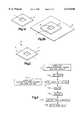
- FIG. 1(a)is a perspective view of a compact of a surrounding body powder composition with a cavity formed therein in accordance with the present invention
- FIG. 1(b)is a perspective view of the compact of FIG. 1(a) showing loose insert powder composition placed within the cavity in accordance with the preferred embodiment of the invention
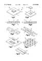
- FIG. 2is a perspective view of a functionally-graded metal substrate having two discrete portions of material composition in the x-y plane;
- FIG. 3is a flow scheme of the process for making functionally-graded metal substrates in accordance with the preferred embodiment of the invention herein;
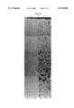
- FIG. 4is a scanning electronic microscope (SEM) micrograph of a cross-section of the functionally-graded metal substrate herein which shows the microstructure of the surrounding body designated by vertical (a) portion of micrograph, and the microstructure of functional insert designated by vertical (b) portion of the micrograph;
- SEMscanning electronic microscope
- FIG. 5is a perspective view of a chip mounted directly onto the functional insert portion of the functionally-graded metal substrate for microelectronic packaging;
- FIG. 6is a perspective view of a compact containing functional insert powder composition prior to placement within the cavity of the compact of surrounding body powder composition in accordance with another embodiment of the invention
- FIG. 7is a cross-sectional view of a functionally-graded metal substrate showing a functional insert that has a tapered cross-sectional width
- FIG. 8is a cross-sectional view of a functionally-graded metal substrate showing a functional insert that extends from one surface of the substrate to another location within the surrounding body of the substrate;
- FIG. 9is a perspective view of the functionally-graded metal substrate of another embodiment of the invention.
- FIG. 10is a perspective view of the functionally-graded metal substrate of another embodiment of the invention showing the functional inserts
- FIG. 11is a perspective view of a functionally-graded metal substrate that has a plurality of functional inserts of varying sizes in accordance with the invention herein;
- FIG. 12is a perspective view of an array of functionally-graded metal substrates in accordance with the invention herein.
- FIG. 13is a perspective view of a functionally-graded metal substrate of the invention herein showing the surrounding body surrounds the functional insert in one dimension.
- the invention hereinprovides for a process for making a functionally-graded metal substrate and the resulting substrate that has at least two discrete areas, a functional insert and a surrounding body, in the x-y plane.
- the functional insertis surrounded by the surrounding body, preferably, in at least two dimensions.
- the discrete areas of the functionally-graded metal substratehave distinct physical characteristics which are governed by the metal composition in each discrete area.
- the functionally-graded metal substratecomprises at least two metal compositions that represent at least one surrounding body and at least one functional insert.
- Metals that make up the surrounding body and the functional insertcan include an elemental metal, a metallic alloy or a metal matrix composite (MMC).
- MMCmetal matrix composite
- the functional insert and the a surrounding bodymay include the same metals but in varying concentrations or compositions.
- Materials that can be used according to the invention hereininclude, for example: metals such as copper, nickel, iron, beryllium, aluminum, silver; metallic alloys such as copper beryllium, copper-zinc (bronze), copper-tin (brass), 64% iron/36% nickel (InvarTM) and 54% iron/29% nickel/17% cobalt (KovarTM), copper-iron, nickel-niobium, nickel-silver, nickel-copper, iron-copper, iron-copper-carbon, iron-copper-nickel, iron-chromium, iron-copper-tin, copper-nickel-titanium-aluminum, nickel-copper-titanium; and metal matrix composites such as copper/tungsten, copper/molybdenum, aluminum/silicon carbide, aluminum/aluminum nitride, copper/aluminum, silver/InvarTM, copper/cubic boron nitride, copper/diamond and copper/high conductivity carbon fiber.
- a heat-generating componentfor example, a chip
- the functional insertis attached directly to the functional insert and the functional insert is surrounded by the surrounding body.
- the functional insertpreferably has a thermal conductivity that is greater than the thermal conductivity of the surrounding body, and the surrounding body preferably has a CTE that is lower than the CTE of the functional insert.
- the surrounding bodythus controls or constrains the expansion of a functional insert along its bonded surfaces as the functional insert conducts heat away from the heat-generating component.
- a process for making a functionally-graded metal substratecomprises: filling the cavity of a metal body with a functional insert and sintering the metal body and the functional insert simultaneously.
- the processfurther comprises infiltrating the sintered metal body or the sintered functional insert or both with a molten metal compound.
- the resultis a functionally-graded metal substrate having a functional insert and a surrounding body that surrounds the functional insert, preferably in at least two dimensions, in the x-y plane.
- the metal bodyis made from a compact of a surrounding body powder composition
- the functional insertis made from a functional insert powder composition.
- FIG. 1(a)shows a surrounding body powder composition 2, which is pressed preferably with cavity 4 formed therein.
- FIG. 1(b)shows the pressed compact containing the surrounding body powder composition on alumina sintering plate or sagger plate 6 and functional insert powder composition 8 in cavity 4.
- Functional insert powder composition 8is preferably a spray-dried powder and is placed in a loosely packed arrangement.
- Metal powders that can be used for the surrounding body powder composition and the functional insert powder compositioncan be any metal powders that are used in metal sintering processes and are well known in the art.
- the sintering plateis then placed in a sintering furnace and fired at a temperature such that sintering causes the insert powder composition to bond with the surrounding body powder composition.
- the surrounding body powder compositionis sintered to a density that is at least 90% of theoretical, preferably at least 97% of theoretical, and even more preferably at least 99% of theoretical.
- the sintered functional insert compositionis porous after sintering having a density that is less than the density of the sintered surrounding body and preferably about 70% or less of theoretical.
- the sintered functional insert compositionis infiltrated with molten metal such that the sintered functional insert achieves a density of at least 90% of theoretical, preferably at least 97% of theoretical, and even more preferably at least 99% of theoretical.
- the resultis a functionally-graded metal substrate having a functional insert and a surrounding body that surrounds the functional insert in at least two dimensions.
- the compact of surrounding body powder compositioncontains copper and tungsten powder comprising from about 5% to about 50% by weight copper, preferably, from about 5% to about 40%, and more preferably, from about 10% to about 30% by weight copper powder.
- Coppercan be introduced in the compact in the form of copper powder or copper oxide powder or both.
- the functional insert powder compositioncomprises copper and tungsten powder that is from about 20% to about 80% by weight copper, preferably, from about 30% to about 50%, and more preferably, from about 30% to about 45% by weight copper powder.
- the functional insert powder compositionis preferably sintered in loose powder form.
- the sintered functional insert compositionis relatively porous infiltrated preferably with copper, and more preferably, oxygen-free high conductivity (OFHC) copper. Infiltration is conducted in a nitrogen/hydrogen environment at a temperature ranging between about 1100° C. and about 1150° C. to produce a functional core having high thermal conductivity relative to the surrounding body.
- OFHCoxygen-free high conductivity
- the compact of surrounding body powder compositioncontains copper and molybdenum powder comprising from about 5% to about 50% by weight copper, preferably, from about 5% to about 40%, and more preferably, from about 10% to about 30% by weight copper powder.
- Coppercan be introduced in the compact in the form of copper powder or copper oxide powder or both.
- the functional insert powder compositioncomprises copper and molybdenum powder that is from about 20% to about 80% by weight copper, preferably, from about 30% to about 50%, and more preferably, from about 30% to about 45% by weight copper powder.
- the functional insert powder compositionis preferably sintered in loose powder form.
- the sintered functional insert compositionis relatively porous infiltrated preferably with copper, and more preferably, oxygen-free high conductivity (OFHC) copper. Infiltration is conducted in a nitrogen/hydrogen environment at a temperature ranging between about 1100° C. and about 1150° C. to produce a functional core having high thermal conductivity relative to the surrounding body.
- OFHCoxygen-free high conductivity
- FIG. 3illustrates a flow scheme that summarizes the process for making copper/tungsten or copper/molybdenum functionally-graded metal substrates for microelectronic packages in accordance with the preferred embodiment of the invention.
- Copper/tungsten or copper/molybdenum spray dried powderis prepared 101 and then dry pressed to form a compact of the surrounding body having at least one cavity therein 102.
- Copper/tungsten functional insert powdercomprising from about 20% to about 80% by weight copper is spray dried 103 and the functional insert powder composition in loose powder form, is placed in the cavity of the compact of the surrounding body powder composition 104.
- the compact of the surrounding body and the functional insert powder compositionsare fired in a furnace during the sintering process 105.
- the functional insert compositionundergoes infiltration 106 with copper to produce a functionally-graded metal substrate. Subsequently, the surfaces of the metal substrate are ground to desired dimensions 107 followed by metal plating 108 in preparation for further processing of the microelectronic package.
- FIG. 4is a scanning electronic microscope (SEM) micrograph of a cross-sectional area of the functionally-graded metal substrate in accordance with the invention herein.
- the surrounding body portion designated by vertical (a) portion of the micrographcontains copper/tungsten metal matrix composite containing from about 15% by weight copper and about 85% by weight tungsten.
- the functional insert portion designated by vertical (b) portion of the micrographis a copper/tungsten metal matrix composite containing from about 40% by weight copper and about 60% by weight tungsten.
- FIG. 5illustrates functionally-graded metal substrate 10 as a carrier substrate of a microelectronic package 20.
- Heat-generating chip 22is attached directly to functional insert 14 by brazing, soldering, epoxy adhesive or attachment means that are well known in the art.
- Functional insert 14conducts heat away from heat-generating chip 22 to the environment or to a heat sink attached thereon (not shown).
- functional insert 14has a thermal conductivity that is greater than the thermal conductivity of the surrounding body and surrounding body 12 has a CTE that is lower than the CTE of functional insert 14.
- the CTE of surrounding bodyapproximately matches or is slightly greater than the CTE of the heat-generating chip and controls the expansion of the functional insert during thermal cycling.
- a metal substrate having a functional insert with high thermal conductivityimproves the thermal dissipation of the metal substrate while maintaining low thermal expansion in the area where the chip is attached.
- the dimensions of the compactare determined by the size of the desired finished part and the die, taking into account the shrinkage of the compact during the sintering operation.
- Sinteringis preferably accomplished using either a batch furnace or a continuous pusher type furnace. Sintering residence time and temperature depends upon the melting temperature or the eutectic temperature of the metal powder composition. The sintering temperature is greater than at least one metal of the powder metal compositions. Infiltration is well known in the art and metal compositions that are used for infiltration are generally those having a melting temperature of about 1400 deg. C or less.
- one of the powder compositions that is usedcontains a metal that is capable of forming a eutectic composition, then a denser substrate can be produced. This phenomenon is described in U.S. Pat. No. 5,686,676 which is hereby incorporated by reference herein.
- An example of a powder metal system that can form a eutectic composition during sinteringis copper-copper oxide. Sintering compacts containing copper oxide or a combination of copper and copper oxide is conducted at temperatures from about 1050° C. to about 1400° C. Even more preferably, the compacts can be sintered in a reducing atmosphere, which for example, contains hydrogen, nitrogen or moisture, for example.
- the processcomprises: compacting a surrounding body powder composition to form a compact having a cavity therein, compacting a functional insert powder composition, filling the cavity with the compact of functional insert powder composition, and sintering the functional insert powder composition and the surrounding body powder composition simultaneously.
- the cavitycan be formed in the compact of surrounding body powder composition while forming the compact or after the compact is formed.
- FIG. 6shows a compact containing functional insert powder composition 8 before it is placed into a compact containing surrounding body powder composition 2.
- the functional insert powder compositionis pressed to a size that will fit into the cavity of the surrounding body composition.
- the two compactsare sintered together to a density that is at least about 90% of theoretical, preferably at least about 97% and at least about 99% of theoretical.
- Both powder metal compositionscan be pressed in a single tool.
- a multi-action press having a specialized feedshoe (receptacle on tool to fill cavities)can be used to press both powder metal compositions in a single tool.
- the processcomprises: compacting a surrounding body powder composition to form a compact having a cavity therein, compacting a functional insert powder composition, filling the cavity with the compact of functional insert powder composition, sintering the functional insert powder composition and the surrounding body powder composition simultaneously, and infiltrating the sintered surrounding body or the sintered functional core or both.
- the metal bodyis a solid, wrought metal body.
- the process for making a functionally-graded metal substratecomprises: placing a functional insert powder composition into the cavity of a solid surrounding body and sintering the functional insert powder composition.
- the cavitycan be formed by machining the solid surrounding body or by other well-known techniques.
- the processfurther comprises infiltrating the sintered functional insert with a molten metal composition.
- the process for making a functionally-graded metal substratecomprises: placing a solid functional insert into the cavity of a solid surrounding body and brazing the solid functional insert to the solid surrounding body.
- the cavitycan be formed by machining the solid surrounding body or by other well-known techniques.
- the solid, functional insertpreferably a wrought metal, is attached or bonded to the metal body using conventional brazing technology.
- the solid functional insertcan be attached by either pressure-assisted or pressureless diffusion bonding to form a functionally-graded metal substrate.
- the functionally-graded metal substrateAfter the functionally-graded metal substrate is made, it can undergo one or more secondary operations. End use dimensions can be achieved by double-disk grinding the metal substrate according to a process well known in the art.
- the functionally-graded metal substratecan also be plated by conventional plating processes, such as electroless plating or electrolytic plating, for example. More specifically, in a microelectronic packaging application, the functionally-graded metal substrate can be nickel plated or nickel and gold plated via electroless or electrolytic plating operations.
- the functional insert of the functionally-graded metal substratecan be any geometric shape.
- FIG. 7shows functional insert 14 has tapered or angled walls.
- the cross-sectional area of the functional coreis increasingly larger toward the bottom of the functionally-graded metal substrate.
- the taperingcan facilitate greater thermal dissipation from the top down if a heat-generating component is attached to functional insert 14, for example.
- the functional insertcan extend partially or completely through the surrounding body.
- the functional insert of FIG. 7shows that the functional insert extends from top surface 15 of functionally-graded metal substrate 10 to bottom surface 16.
- FIG. 8shows functional insert 14 extends from the top surface of substrate 10 to a location within surrounding body 12.
- Functionally-graded metal substratescan be made in a variety of shapes, sizes and configuration as shown in FIG. 9 and FIG. 10.
- the functionally-grade metal substrate hereincan have one or many functional inserts.
- FIG. 11shows a functionally-graded metal substrate that has a plurality of functional inserts of varying sizes and shapes. If used in microelectronic packaging, the functionally-graded metal substrate can house several components such as dice, diodes, resistors, and capacitors, for example.
- the functional insertscan be distributed throughout the substrate wherever needed per end use requirements. Limitations on the size of the functional insert or the volume of functional insert relative to the total volume of the functionally-graded metal substrate depends upon the end use application, desired performances, and the functional insert and surrounding metal compositions.
- the volume of the functional insert relative to the total volume of the substratemust be large enough to physically accommodate a heat-generating component and to facilitate improved heat transfer.
- the surrounding bodymust be large enough to constrain the dimensional expansion of the functional insert which has a CTE that is greater than the surrounding body.
- functionally-graded metal substratescan be made in an array which consists of a repeated pattern of metal substrates.
- An array of functionally-graded metal substratesis illustrated in FIG. 12.
- a large, functionally-graded metal substratecan be prescribed so that the array can be singulated into several individual metal substrates having a functional insert 14 and a surrounding body 12.
- FIG. 13is a perspective view of a functionally-graded metal substrate in which the surrounding body 24 surrounds 26 the functional insert in one dimension.
- a copper/tungsten (15%/85% by weight) spray dried powderwas made using the quantity of ingredients listed below.
- Benzotriazole corrosion inhibitor(Cobratec® 99 available from PMC Specialties Group, Inc., Cincinnati, Ohio) was dissolved in isopropyl alcohol and particulate cuprous oxide was then added to the benotriazole solution. The mixture was set aside for 12 hours.
- Deionized water and cobalt metalwere mixed in a mixing tank for ten minutes.
- tungsten metal(mean particle size of about one micron) was ball milled for about four hours and then slowly added to the ingredients in the mixing tank and mixed for two hours.
- the mixture of cuprous oxide, benzotriazole and isopropyl alcoholwas added and mixed for 30 minutes.
- Rhoplex® B-60A acrylic emulsionwas then added to the mixture which was then mixed for an additional 30 minutes.
- the mixturewas recovered and spray dried in a Bowen No. 1 Tower spray drier at 25 psi and an outlet temperature of about 270° C. to about 280° C.
- the spray dried agglomerate powderwhich after screening (65 mesh) exhibited a Hall meter flow rate of about 30 seconds per 50 grams of powder.
- a copper/tungsten (30%/70% by weight) functional powder compositionwas made by first making spray dried tungsten. Teledyne C-10 tungsten powder (306.8 grams) and deionized water (88 grams) were milled in a tumbling ball mill for three hours until the particle size of the tungsten was finer than about 10 microns. An acrylic emulsion, Rhoplex® B-60A, made by Rohm and Haas was screened through a 100 mesh screen before being weighed out in an amount of 5.2 grams. The Rhoplex was slowly added to the tungsten slurry and mixed for a minimum of ten minutes.
- the mixturewas then spray dried in a Bowen No. 1 Tower spray drier at 25 psi and an outlet temperature of about 270-280° C.
- the spray dried agglomerate powder after screening(65 mesh) exhibited a Hall flow rate of about 20 seconds per 50 grams of powder.
- the spray dried tungsten powder(70 grams) was then blended with RL copper powder (30 grams) made by OMG Metal Products, Research Triangle Park, N. C. in a blending jar with a disrupter bar and blended for 5 minutes. The mixture was then screened through a 60 mesh screen.
- Green compacts of the surrounding body powder compositionwere made by filling a die with copper/tungsten (15%/85%) powder from Step A and compressing the powder in a press at a pressure of 25,000 psi to form a green compact.
- the diewas rectangular in shape and had a solid rectangular shaft built within.
- the resulting green compacthad a through-hole that extended the thickness of the compact.
- the green compactwas placed on alumina setter plates and the entire volume of the hole was filled with the functional powder composition described in step B above.
- the compactwas sintered in a BTU reducing furnace at 1125° C. at a rate of one inch/min of the compact.
- the atmosphere in the BTU furnacewas 100% hydrogen having a dew point of +20° C.
- the resulting sintered flangewas placed on the setter for the infiltrating furnace.
- Oxygen-free high conductivity (OFHC) copper compacts or preformswere prepared for infiltration. Approximately 20% in excess of OFHC copper was placed on the area of the flange to be infiltrated, that is, the surface area of the flange that, prior to sintering, consisted of the functional powder composition.
- the sintered flangewas then heated to 1100° C. in a dry ( ⁇ -400C.) hydrogen/nitrogen (25%/75%) atmosphere for about 5 minutes. The result was a functionally-graded metal substrate having a functional insert and a surrounding body.
- the proper flatness and desired thickness of the functionally-graded metal substratewas achieved by double-disc grinding the surfaces.
- the heat sinkwas tumbled to remove the burrs.
- the metal substratewas nickel plated by the well-known electroless nickel plating process (plate/sinter/plate/sinter process) to a thickness of about 100 micro-inches of nickel.
- the metal substratewas electrolytically plated with gold to a thickness of about 75 micro inches and a flatness of about 0.2 to about 0.3 mils/inch.
- the functional insert and the surrounding body of the functionally-graded metal substrate embodiments described hereincan comprise a variety of metal compositions for use in end-use applications other than microelectronic applications. It is to be understood, however, that changes may be made in the particular embodiments described above which are within the full-intended scope of the invention as defined in the appended claims.
Landscapes
- Engineering & Computer Science (AREA)
- Chemical & Material Sciences (AREA)
- Materials Engineering (AREA)
- Computer Hardware Design (AREA)
- Condensed Matter Physics & Semiconductors (AREA)
- General Physics & Mathematics (AREA)
- Physics & Mathematics (AREA)
- Microelectronics & Electronic Packaging (AREA)
- Power Engineering (AREA)
- Composite Materials (AREA)
- Manufacturing & Machinery (AREA)
- Mechanical Engineering (AREA)
- Powder Metallurgy (AREA)
- Cooling Or The Like Of Semiconductors Or Solid State Devices (AREA)
Abstract
Description
______________________________________ Tungsten 423.6 lbs Cuprous Oxide 84.0 lbs Deionized water 105.1 lbs Cobalt 2.7 lbs Isopropyl Alcohol 18.5 lbs Benzotriazole 3.3 lbs Acrylic Emulsion 12.5 lbs ______________________________________
Claims (41)
Priority Applications (4)
| Application Number | Priority Date | Filing Date | Title |
|---|---|---|---|
| US09/148,126US6114048A (en) | 1998-09-04 | 1998-09-04 | Functionally graded metal substrates and process for making same |
| EP99944063AEP1113894A1 (en) | 1998-09-04 | 1999-09-02 | Functionally graded metal substrates and process for making same |
| PCT/US1999/020157WO2000013823A1 (en) | 1998-09-04 | 1999-09-02 | Functionally graded metal substrates and process for making same |
| JP2000568614AJP2002524862A (en) | 1998-09-04 | 1999-09-02 | Functionally classified metal substrate and process for making it |
Applications Claiming Priority (1)
| Application Number | Priority Date | Filing Date | Title |
|---|---|---|---|
| US09/148,126US6114048A (en) | 1998-09-04 | 1998-09-04 | Functionally graded metal substrates and process for making same |
Publications (1)
| Publication Number | Publication Date |
|---|---|
| US6114048Atrue US6114048A (en) | 2000-09-05 |
Family
ID=22524400
Family Applications (1)
| Application Number | Title | Priority Date | Filing Date |
|---|---|---|---|
| US09/148,126Expired - Fee RelatedUS6114048A (en) | 1998-09-04 | 1998-09-04 | Functionally graded metal substrates and process for making same |
Country Status (4)
| Country | Link |
|---|---|
| US (1) | US6114048A (en) |
| EP (1) | EP1113894A1 (en) |
| JP (1) | JP2002524862A (en) |
| WO (1) | WO2000013823A1 (en) |
Cited By (58)
| Publication number | Priority date | Publication date | Assignee | Title |
|---|---|---|---|---|
| US6252295B1 (en)* | 2000-06-19 | 2001-06-26 | International Business Machines Corporation | Adhesion of silicon carbide films |
| US6295200B1 (en)* | 2000-02-23 | 2001-09-25 | Motorola, Inc. | Carrier assembly and method |
| US6355362B1 (en)* | 1999-04-30 | 2002-03-12 | Pacific Aerospace & Electronics, Inc. | Electronics packages having a composite structure and methods for manufacturing such electronics packages |
| US6361857B1 (en)* | 1998-01-16 | 2002-03-26 | Sumitomo Electric Industries, Ltd. | Heatsink and fabrication method thereof |
| US6404048B2 (en)* | 1998-09-03 | 2002-06-11 | Micron Technology, Inc. | Heat dissipating microelectronic package |
| US6533554B1 (en)* | 1999-11-01 | 2003-03-18 | University Of Southern California | Thermal transpiration pump |
| US6569380B2 (en)* | 2001-08-27 | 2003-05-27 | Advanced Materials Technologies Pte, Ltd. | Enclosure for a semiconductor device |
| WO2003005093A3 (en)* | 2001-07-02 | 2003-08-14 | Zentrix Technologies Inc | Carrier sub-assembly with inserts for optoelectronic device coupling |
| US6611056B2 (en)* | 1999-03-16 | 2003-08-26 | Hitachi, Ltd. | Composite material, and manufacturing method and uses of same |
| US20030171006A1 (en)* | 2002-03-08 | 2003-09-11 | Vadim Gektin | Apparatus and methods for enhancing thermal performance of integrated circuit packages |
| US20030178177A1 (en)* | 2002-03-21 | 2003-09-25 | Eytcheson Charles T. | Heatsink buffer configuration |
| US6637506B2 (en)* | 2002-03-08 | 2003-10-28 | Sun Microsystems, Inc. | Multi-material heat spreader |
| US20030224554A1 (en)* | 2002-03-22 | 2003-12-04 | Arndt Ludtke | Package with a substrate of high thermal conductivity |
| FR2844397A1 (en)* | 2002-09-06 | 2004-03-12 | Toyota Jidoshokki Kk | Low expansion unit for use as heat diffuser in semiconductor equipment includes an iron plate element, and a layer of iron/nickel |
| US6727117B1 (en) | 2002-11-07 | 2004-04-27 | Kyocera America, Inc. | Semiconductor substrate having copper/diamond composite material and method of making same |
| US20040093985A1 (en)* | 2000-09-06 | 2004-05-20 | Carton Eric Peter | Hard metal body with hardness gradient, such as punching tools |
| US20040119161A1 (en)* | 2002-12-18 | 2004-06-24 | Sumitomo Electric Industries, Ltd. | Package for housing semiconductor chip, fabrication method thereof and semiconductor device |
| US20040135247A1 (en)* | 2001-08-31 | 2004-07-15 | Kouichi Takashima | Semicoductor radiating substrate and production method therefor and package |
| US20040173901A1 (en)* | 2003-03-05 | 2004-09-09 | Intel Corporation | Thermally enhanced electronic flip-chip packaging with external-connector side die and method |
| US20040195662A1 (en)* | 2003-01-10 | 2004-10-07 | Kyocera America, Inc. | Semiconductor package having non-ceramic based window frame |
| US20040264137A1 (en)* | 2003-06-26 | 2004-12-30 | Trautman Mark A | Low noise heatsink |
| US20040261980A1 (en)* | 2003-06-30 | 2004-12-30 | Dani Ashay A. | Heat dissipating device with preselected designed interface for thermal interface materials |
| US20050006054A1 (en)* | 2002-01-16 | 2005-01-13 | Ryuuji Miyazaki | Heat sink having high efficiency cooling capacity and semiconductor device comprising it |
| US20060219056A1 (en)* | 2005-03-29 | 2006-10-05 | Larink Steven C Jr | Metal powders and methods for producing the same |
| US7215545B1 (en)* | 2003-05-01 | 2007-05-08 | Saeed Moghaddam | Liquid cooled diamond bearing heat sink |
| US20070158834A1 (en)* | 2006-01-10 | 2007-07-12 | Schultz Roger L | Electrical connections made with dissimilar metals |
| CN100355924C (en)* | 2003-09-05 | 2007-12-19 | 上海材料研究所 | Tungsten copper functional composite material and its preparation technology |
| US20080030960A1 (en)* | 2005-07-05 | 2008-02-07 | International Business Machines Corporation | Anisotropic heat spreading apparatus and method for semiconductor devices |
| US20080113877A1 (en)* | 2006-08-16 | 2008-05-15 | Intematix Corporation | Liquid solution deposition of composition gradient materials |
| US20080174007A1 (en)* | 2003-03-31 | 2008-07-24 | Intel Corporation | Heat sink with preattached thermal interface material and method of making same |
| US20080308917A1 (en)* | 2007-06-13 | 2008-12-18 | Infineon Technologies Ag | Embedded chip package |
| US20090040727A1 (en)* | 2007-08-07 | 2009-02-12 | Continental Automotive Gmbh | Circuit Carrier Structure with Improved Heat Dissipation |
| CN100464001C (en)* | 2006-04-11 | 2009-02-25 | 中国科学院金属研究所 | A high-strength, high-conductivity, oxidation-resistant low-silver copper-based alloy and its preparation |
| US20090159451A1 (en)* | 2007-12-20 | 2009-06-25 | Integran Technologies Inc. | Variable property electrodepositing of metallic structures |
| US20090188789A1 (en)* | 2008-01-11 | 2009-07-30 | Climax Engineered Materials, Llc | Sodium/molybdenum powder compacts and methods for producing the same |
| US20090236730A1 (en)* | 2008-03-19 | 2009-09-24 | Roden Topacio | Die substrate with reinforcement structure |
| US20100052188A1 (en)* | 2008-08-26 | 2010-03-04 | Mohammad Khan | Semiconductor Chip with Solder Joint Protection Ring |
| US20100139885A1 (en)* | 2008-12-09 | 2010-06-10 | Renewable Thermodynamics, Llc | Sintered diamond heat exchanger apparatus |
| GB2468054A (en)* | 2006-03-24 | 2010-08-25 | Climax Engineered Mat Llc | Molybdenum powder and a method of making metal powder |
| US20100236688A1 (en)* | 2009-03-20 | 2010-09-23 | Scalzo Orlando | Process for joining powder injection molded parts |
| US20100276799A1 (en)* | 2009-05-04 | 2010-11-04 | Heng Stephen F | Semiconductor Chip Package with Stiffener Frame and Configured Lid |
| US20100295077A1 (en)* | 2009-05-19 | 2010-11-25 | Intematix Corporation | Manufacture of light emitting devices with phosphor wavelength conversion |
| US20110250467A1 (en)* | 2010-04-13 | 2011-10-13 | Lawrence Livermore National Security, Llc | Methods of three-dimensional electrophoretic deposition for ceramic and cermet applications and systems thereof |
| US20120063071A1 (en)* | 2008-09-08 | 2012-03-15 | Materials And Electrochemical Research (Mer) Corporation | Machinable metal/diamond metal matrix composite compound structure and method of making same |
| US20120161309A1 (en)* | 2010-12-28 | 2012-06-28 | Mitsubishi Electric Corporation | Semiconductor package |
| DE102011002458A1 (en)* | 2011-01-05 | 2012-07-05 | Robert Bosch Gmbh | Electronic assembly with improved thermal management |
| US20120269218A1 (en)* | 2011-04-22 | 2012-10-25 | Lawrence Livermore National Security, Llc | Stabilization of green bodies via sacrificial gelling agent during electrophoretic deposition |
| US20120312519A1 (en)* | 2011-06-10 | 2012-12-13 | Rogers Corporation | Partially composite plate |
| DE102011081687A1 (en)* | 2011-08-26 | 2013-02-28 | Robert Bosch Gmbh | Semiconductor device with a heat sink |
| US20130109788A1 (en)* | 2011-11-01 | 2013-05-02 | Shinano Electric Refining Co., Ltd. | Spherical alpha silicon carbide, the method for manufacturing the same, and a sintered body as well as an organic resin-based composite made from the silicon carbide |
| CN104726735A (en)* | 2013-12-23 | 2015-06-24 | 北京有色金属研究总院 | Composite-structure highly-oriented heat conducting material and preparation method thereof |
| EP2902704A1 (en)* | 2014-01-31 | 2015-08-05 | Christie Digital Systems Canada, Inc. | A light emitting device with a heat sink composed of two materials |
| US9852824B2 (en) | 2010-08-24 | 2017-12-26 | Lawrence Livermore National Security, Llc | Methods for controlling pore morphology in aerogels using electric fields and products thereof |
| US9867282B2 (en) | 2013-08-16 | 2018-01-09 | Ati Technologies Ulc | Circuit board with corner hollows |
| US9970318B2 (en) | 2014-06-25 | 2018-05-15 | Pratt & Whitney Canada Corp. | Shroud segment and method of manufacturing |
| CN108701666A (en)* | 2016-02-19 | 2018-10-23 | 贺利氏德国有限两合公司 | Method, underboarding, the method for manufacturing semiconductor module and semiconductor module for manufacturing underboarding |
| US10347798B2 (en) | 2015-06-01 | 2019-07-09 | Intematix Corporation | Photoluminescence material coating of LED chips |
| WO2019191457A1 (en)* | 2018-03-29 | 2019-10-03 | Macom Technology Solutions Holdings, Inc. | Substrate with embedded copper molybdenum or copper tungsten heat slug |
Families Citing this family (11)
| Publication number | Priority date | Publication date | Assignee | Title |
|---|---|---|---|---|
| JP3841633B2 (en) | 2000-10-16 | 2006-11-01 | ヤマハ株式会社 | Semiconductor laser module |
| JP2003068954A (en)* | 2001-08-28 | 2003-03-07 | Kyocera Corp | Package for storing semiconductor elements |
| JP4514598B2 (en)* | 2004-09-28 | 2010-07-28 | 京セラ株式会社 | Electronic component storage package and electronic device |
| JP2009224715A (en)* | 2008-03-18 | 2009-10-01 | Toyota Central R&D Labs Inc | Heat dissipation plate, and module equipped with the same |
| US7754533B2 (en) | 2008-08-28 | 2010-07-13 | Infineon Technologies Ag | Method of manufacturing a semiconductor device |
| US8637379B2 (en) | 2009-10-08 | 2014-01-28 | Infineon Technologies Ag | Device including a semiconductor chip and a carrier and fabrication method |
| DE102013102541A1 (en)* | 2013-03-13 | 2014-09-18 | Schweizer Electronic Ag | Electronic component, method for its production and printed circuit board with electronic component |
| JP2015032758A (en)* | 2013-08-05 | 2015-02-16 | 日本発條株式会社 | Heat sink, power module and method of manufacturing heat sink |
| US20170241429A1 (en)* | 2014-05-30 | 2017-08-24 | Nuovo Pignone Srl | Method of manufacturing a component of a turbomachine, component of turbomachine and turbomachine |
| CN110964983B (en)* | 2019-12-30 | 2021-05-18 | 吉林大学 | FeCuSn-based composite alloy powder for diamond products and preparation method thereof |
| CN112226703B (en)* | 2020-10-19 | 2021-08-10 | 有研工程技术研究院有限公司 | Diamond/copper composite material and preparation method thereof |
Citations (32)
| Publication number | Priority date | Publication date | Assignee | Title |
|---|---|---|---|---|
| US3399332A (en)* | 1965-12-29 | 1968-08-27 | Texas Instruments Inc | Heat-dissipating support for semiconductor device |
| US3590327A (en)* | 1969-04-24 | 1971-06-29 | Transmation Inc | System for maintaining uniform temperature conditions throughout a body |
| US3694699A (en)* | 1970-03-30 | 1972-09-26 | Nat Beryllia Corp | Ceramic based substrates for electronic circuits with improved heat dissipating properties and circuits including the same |
| US3801381A (en)* | 1968-08-27 | 1974-04-02 | Surface Technology Corp | Composite nitrided articles |
| US3840889A (en)* | 1973-07-11 | 1974-10-08 | Rca Corp | Laser diode package formed of ceramic and metal materials having high electrical and thermal conductivity |
| US3870776A (en)* | 1973-01-02 | 1975-03-11 | Metalized Ceramics Corp | Method for making ceramic-metal structures |
| US4025997A (en)* | 1975-12-23 | 1977-05-31 | International Telephone & Telegraph Corporation | Ceramic mounting and heat sink device |
| US4066839A (en)* | 1972-11-16 | 1978-01-03 | Sgs-Ates Componenti Elettronici S.P.A. | Molded body incorporating heat dissipator |
| US4589542A (en)* | 1983-12-19 | 1986-05-20 | The Boeing Company | Cargo drive unit |
| US4811166A (en)* | 1986-07-02 | 1989-03-07 | Texas Instruments Incorporated | Heat dissipating member for mounting a semiconductor device and electrical circuit unit incorporating the member |
| US4859542A (en)* | 1986-09-18 | 1989-08-22 | The British Petroleum Company P.L.C. | Graded structure composites |
| US4866571A (en)* | 1982-06-21 | 1989-09-12 | Olin Corporation | Semiconductor package |
| US4870377A (en)* | 1987-11-27 | 1989-09-26 | General Electric Company | Electronic circuit substrate construction |
| US5008737A (en)* | 1988-10-11 | 1991-04-16 | Amoco Corporation | Diamond composite heat sink for use with semiconductor devices |
| EP0424858A2 (en)* | 1989-10-23 | 1991-05-02 | Mitsubishi Denki Kabushiki Kaisha | Semiconductor device and soldering method employable in manufacturing the same |
| US5049184A (en)* | 1990-12-17 | 1991-09-17 | Carpenter Technology Corporation | Method of making a low thermal expansion, high thermal conductivity, composite powder metallurgy member and a member made thereby |
| US5099310A (en)* | 1982-07-26 | 1992-03-24 | Sumitomo Electric Industries, Ltd. | Substrate for semiconductor apparatus |
| US5113315A (en)* | 1990-08-07 | 1992-05-12 | Cirqon Technologies Corporation | Heat-conductive metal ceramic composite material panel system for improved heat dissipation |
| US5126102A (en)* | 1990-03-15 | 1992-06-30 | Kabushiki Kaisha Toshiba | Fabricating method of composite material |
| US5130771A (en)* | 1988-10-11 | 1992-07-14 | Amoco Corporation | Diamond composite heat sink for use with semiconductor devices |
| US5200641A (en)* | 1990-10-04 | 1993-04-06 | Mitsubishi Denki Kabushiki Kaisha | Semiconductor device structure including bending-resistant radiating layer |
| US5355281A (en)* | 1993-06-29 | 1994-10-11 | E.B.G. Elektronische Bauelemente Gesellschaft M.B.H. | Electrical device having a bonded ceramic-copper heat transfer medium |
| US5386339A (en)* | 1993-07-29 | 1995-01-31 | Hughes Aircraft Company | Monolithic microelectronic circuit package including low-temperature-cofired-ceramic (LTCC) tape dielectric structure and in-situ heat sink |
| US5493153A (en)* | 1992-11-26 | 1996-02-20 | Tokyo Tungsten Co., Ltd. | Plastic-packaged semiconductor device having a heat sink matched with a plastic package |
| US5514327A (en)* | 1993-12-14 | 1996-05-07 | Lsi Logic Corporation | Powder metal heat sink for integrated circuit devices |
| US5552232A (en)* | 1994-12-21 | 1996-09-03 | International Business Machines Corporation | Aluminum nitride body having graded metallurgy |
| US5608267A (en)* | 1992-09-17 | 1997-03-04 | Olin Corporation | Molded plastic semiconductor package including heat spreader |
| US5623394A (en)* | 1994-12-05 | 1997-04-22 | International Business Machines Corporation | Apparatus for cooling of chips using a plurality of customized thermally conductive materials |
| US5686676A (en)* | 1996-05-07 | 1997-11-11 | Brush Wellman Inc. | Process for making improved copper/tungsten composites |
| US5878322A (en)* | 1993-04-14 | 1999-03-02 | Polese; Frank J. | Heat-dissipating substrate for micro-electronic devices and fabrication method |
| US5886407A (en)* | 1993-04-14 | 1999-03-23 | Frank J. Polese | Heat-dissipating package for microcircuit devices |
| US5886269A (en)* | 1995-02-17 | 1999-03-23 | Nippon Tungsten Co., Ltd. | Substrate and heat sink for a semiconductor and method of manufacturing the same |
Family Cites Families (5)
| Publication number | Priority date | Publication date | Assignee | Title |
|---|---|---|---|---|
| JP2733684B2 (en) | 1989-04-17 | 1998-03-30 | 日本粉末合金株式会社 | Joined sintered friction material |
| US5481136A (en) | 1992-10-28 | 1996-01-02 | Sumitomo Electric Industries, Ltd. | Semiconductor element-mounting composite heat-sink base |
| JPH08186204A (en)* | 1994-11-02 | 1996-07-16 | Nippon Tungsten Co Ltd | Heat sink and method of manufacturing the same |
| JP2912211B2 (en)* | 1995-02-17 | 1999-06-28 | 日本タングステン株式会社 | Semiconductor substrate material and method of manufacturing the same |
| JPH10200208A (en) | 1997-01-09 | 1998-07-31 | Nec Corp | Semiconductor laser module |
- 1998
- 1998-09-04USUS09/148,126patent/US6114048A/ennot_activeExpired - Fee Related
- 1999
- 1999-09-02EPEP99944063Apatent/EP1113894A1/ennot_activeWithdrawn
- 1999-09-02JPJP2000568614Apatent/JP2002524862A/ennot_activeWithdrawn
- 1999-09-02WOPCT/US1999/020157patent/WO2000013823A1/ennot_activeApplication Discontinuation
Patent Citations (34)
| Publication number | Priority date | Publication date | Assignee | Title |
|---|---|---|---|---|
| US3399332A (en)* | 1965-12-29 | 1968-08-27 | Texas Instruments Inc | Heat-dissipating support for semiconductor device |
| US3801381A (en)* | 1968-08-27 | 1974-04-02 | Surface Technology Corp | Composite nitrided articles |
| US3590327A (en)* | 1969-04-24 | 1971-06-29 | Transmation Inc | System for maintaining uniform temperature conditions throughout a body |
| US3694699A (en)* | 1970-03-30 | 1972-09-26 | Nat Beryllia Corp | Ceramic based substrates for electronic circuits with improved heat dissipating properties and circuits including the same |
| US4066839A (en)* | 1972-11-16 | 1978-01-03 | Sgs-Ates Componenti Elettronici S.P.A. | Molded body incorporating heat dissipator |
| US3870776A (en)* | 1973-01-02 | 1975-03-11 | Metalized Ceramics Corp | Method for making ceramic-metal structures |
| US3840889A (en)* | 1973-07-11 | 1974-10-08 | Rca Corp | Laser diode package formed of ceramic and metal materials having high electrical and thermal conductivity |
| US4025997A (en)* | 1975-12-23 | 1977-05-31 | International Telephone & Telegraph Corporation | Ceramic mounting and heat sink device |
| US4866571A (en)* | 1982-06-21 | 1989-09-12 | Olin Corporation | Semiconductor package |
| US5099310A (en)* | 1982-07-26 | 1992-03-24 | Sumitomo Electric Industries, Ltd. | Substrate for semiconductor apparatus |
| US4589542A (en)* | 1983-12-19 | 1986-05-20 | The Boeing Company | Cargo drive unit |
| US4811166A (en)* | 1986-07-02 | 1989-03-07 | Texas Instruments Incorporated | Heat dissipating member for mounting a semiconductor device and electrical circuit unit incorporating the member |
| US4859542A (en)* | 1986-09-18 | 1989-08-22 | The British Petroleum Company P.L.C. | Graded structure composites |
| US4870377A (en)* | 1987-11-27 | 1989-09-26 | General Electric Company | Electronic circuit substrate construction |
| US5008737A (en)* | 1988-10-11 | 1991-04-16 | Amoco Corporation | Diamond composite heat sink for use with semiconductor devices |
| US5130771A (en)* | 1988-10-11 | 1992-07-14 | Amoco Corporation | Diamond composite heat sink for use with semiconductor devices |
| EP0424858A2 (en)* | 1989-10-23 | 1991-05-02 | Mitsubishi Denki Kabushiki Kaisha | Semiconductor device and soldering method employable in manufacturing the same |
| US5126102A (en)* | 1990-03-15 | 1992-06-30 | Kabushiki Kaisha Toshiba | Fabricating method of composite material |
| US5113315A (en)* | 1990-08-07 | 1992-05-12 | Cirqon Technologies Corporation | Heat-conductive metal ceramic composite material panel system for improved heat dissipation |
| US5200641A (en)* | 1990-10-04 | 1993-04-06 | Mitsubishi Denki Kabushiki Kaisha | Semiconductor device structure including bending-resistant radiating layer |
| US5049184A (en)* | 1990-12-17 | 1991-09-17 | Carpenter Technology Corporation | Method of making a low thermal expansion, high thermal conductivity, composite powder metallurgy member and a member made thereby |
| US5608267A (en)* | 1992-09-17 | 1997-03-04 | Olin Corporation | Molded plastic semiconductor package including heat spreader |
| US5493153A (en)* | 1992-11-26 | 1996-02-20 | Tokyo Tungsten Co., Ltd. | Plastic-packaged semiconductor device having a heat sink matched with a plastic package |
| US5886407A (en)* | 1993-04-14 | 1999-03-23 | Frank J. Polese | Heat-dissipating package for microcircuit devices |
| US5878322A (en)* | 1993-04-14 | 1999-03-02 | Polese; Frank J. | Heat-dissipating substrate for micro-electronic devices and fabrication method |
| US5355281A (en)* | 1993-06-29 | 1994-10-11 | E.B.G. Elektronische Bauelemente Gesellschaft M.B.H. | Electrical device having a bonded ceramic-copper heat transfer medium |
| US5386339A (en)* | 1993-07-29 | 1995-01-31 | Hughes Aircraft Company | Monolithic microelectronic circuit package including low-temperature-cofired-ceramic (LTCC) tape dielectric structure and in-situ heat sink |
| US5514327A (en)* | 1993-12-14 | 1996-05-07 | Lsi Logic Corporation | Powder metal heat sink for integrated circuit devices |
| US5623394A (en)* | 1994-12-05 | 1997-04-22 | International Business Machines Corporation | Apparatus for cooling of chips using a plurality of customized thermally conductive materials |
| US5552107A (en)* | 1994-12-21 | 1996-09-03 | Ibm | Aluminum nitride body having graded metallurgy |
| US5552232A (en)* | 1994-12-21 | 1996-09-03 | International Business Machines Corporation | Aluminum nitride body having graded metallurgy |
| US5682589A (en)* | 1994-12-21 | 1997-10-28 | International Business Machines Corporation | Aluminum nitride body having graded metallurgy |
| US5886269A (en)* | 1995-02-17 | 1999-03-23 | Nippon Tungsten Co., Ltd. | Substrate and heat sink for a semiconductor and method of manufacturing the same |
| US5686676A (en)* | 1996-05-07 | 1997-11-11 | Brush Wellman Inc. | Process for making improved copper/tungsten composites |
Non-Patent Citations (1)
| Title |
|---|
| International Search Report for PCT/US99/20157.* |
Cited By (114)
| Publication number | Priority date | Publication date | Assignee | Title |
|---|---|---|---|---|
| US6361857B1 (en)* | 1998-01-16 | 2002-03-26 | Sumitomo Electric Industries, Ltd. | Heatsink and fabrication method thereof |
| US6641861B2 (en) | 1998-01-16 | 2003-11-04 | Sumitomo Electric Industries, Ltd. | Heatsink and fabrication method thereof |
| US6404048B2 (en)* | 1998-09-03 | 2002-06-11 | Micron Technology, Inc. | Heat dissipating microelectronic package |
| US6611056B2 (en)* | 1999-03-16 | 2003-08-26 | Hitachi, Ltd. | Composite material, and manufacturing method and uses of same |
| US6630734B2 (en)* | 1999-03-16 | 2003-10-07 | Hitachi, Ltd. | Composite material, and manufacturing method and uses of same |
| US6355362B1 (en)* | 1999-04-30 | 2002-03-12 | Pacific Aerospace & Electronics, Inc. | Electronics packages having a composite structure and methods for manufacturing such electronics packages |
| US6533554B1 (en)* | 1999-11-01 | 2003-03-18 | University Of Southern California | Thermal transpiration pump |
| US6295200B1 (en)* | 2000-02-23 | 2001-09-25 | Motorola, Inc. | Carrier assembly and method |
| US6252295B1 (en)* | 2000-06-19 | 2001-06-26 | International Business Machines Corporation | Adhesion of silicon carbide films |
| US20040093985A1 (en)* | 2000-09-06 | 2004-05-20 | Carton Eric Peter | Hard metal body with hardness gradient, such as punching tools |
| WO2003005093A3 (en)* | 2001-07-02 | 2003-08-14 | Zentrix Technologies Inc | Carrier sub-assembly with inserts for optoelectronic device coupling |
| US6569380B2 (en)* | 2001-08-27 | 2003-05-27 | Advanced Materials Technologies Pte, Ltd. | Enclosure for a semiconductor device |
| US6979901B2 (en) | 2001-08-31 | 2005-12-27 | Sumitomo Electric Industries, Ltd. | Semiconductor heat-dissipating substrate, and manufacturing method and package therefor |
| US20040135247A1 (en)* | 2001-08-31 | 2004-07-15 | Kouichi Takashima | Semicoductor radiating substrate and production method therefor and package |
| US20050006054A1 (en)* | 2002-01-16 | 2005-01-13 | Ryuuji Miyazaki | Heat sink having high efficiency cooling capacity and semiconductor device comprising it |
| US7431072B2 (en) | 2002-01-16 | 2008-10-07 | Fujitsu Limited | Heat sink with increased cooling capacity and semiconductor device comprising the heat sink |
| US20070107872A1 (en)* | 2002-01-16 | 2007-05-17 | Fujitsu Limited | Heat sink with increased cooling capacity and semiconductor device comprising the hear sink |
| US7219721B2 (en)* | 2002-01-16 | 2007-05-22 | Fujitsu Limited | Heat sink having high efficiency cooling capacity and semiconductor device comprising it |
| US6727193B2 (en) | 2002-03-08 | 2004-04-27 | Sun Microsystems, Inc. | Apparatus and methods for enhancing thermal performance of integrated circuit packages |
| US20030171006A1 (en)* | 2002-03-08 | 2003-09-11 | Vadim Gektin | Apparatus and methods for enhancing thermal performance of integrated circuit packages |
| US6637506B2 (en)* | 2002-03-08 | 2003-10-28 | Sun Microsystems, Inc. | Multi-material heat spreader |
| US20030178177A1 (en)* | 2002-03-21 | 2003-09-25 | Eytcheson Charles T. | Heatsink buffer configuration |
| US6918437B2 (en)* | 2002-03-21 | 2005-07-19 | Delphi Technologies, Inc. | Heatsink buffer configuration |
| US20030224554A1 (en)* | 2002-03-22 | 2003-12-04 | Arndt Ludtke | Package with a substrate of high thermal conductivity |
| US6998180B2 (en)* | 2002-03-22 | 2006-02-14 | Plansee Aktiengesellschaft | Package with a substrate of high thermal conductivity |
| US20050031889A1 (en)* | 2002-09-06 | 2005-02-10 | Takashi Yoshida | Low-expansion unit, method of manufacturing the same and semiconductor provided with the same |
| FR2844397A1 (en)* | 2002-09-06 | 2004-03-12 | Toyota Jidoshokki Kk | Low expansion unit for use as heat diffuser in semiconductor equipment includes an iron plate element, and a layer of iron/nickel |
| US7087316B2 (en) | 2002-09-06 | 2006-08-08 | Kabushiki Kaisha Toyota Jidoshokki | Low-expansion unit, method of manufacturing the same and semiconductor provided with the same |
| EP1576653A4 (en)* | 2002-11-07 | 2008-11-12 | Kyocera America Inc | Semiconductor substrate having copper/diamond composite material and method of making same |
| EP2587536A1 (en)* | 2002-11-07 | 2013-05-01 | Kyocera America, Inc. | Semiconductor substrate having copper/diamond composite material and method of making same |
| US6727117B1 (en) | 2002-11-07 | 2004-04-27 | Kyocera America, Inc. | Semiconductor substrate having copper/diamond composite material and method of making same |
| US20040119161A1 (en)* | 2002-12-18 | 2004-06-24 | Sumitomo Electric Industries, Ltd. | Package for housing semiconductor chip, fabrication method thereof and semiconductor device |
| EP1432029A3 (en)* | 2002-12-18 | 2004-08-04 | Sumitomo Electric Industries, Ltd. | Package for housing a semiconductor chip having a metal-diamond composite in the substrate, and fabrication method thereof |
| US7582964B2 (en) | 2003-01-10 | 2009-09-01 | Kyocera America, Inc. | Semiconductor package having non-ceramic based window frame |
| US20080142963A1 (en)* | 2003-01-10 | 2008-06-19 | Kyocera America, Inc. | Semiconductor Package Having Non-Ceramic Based Window Frame |
| US7298046B2 (en)* | 2003-01-10 | 2007-11-20 | Kyocera America, Inc. | Semiconductor package having non-ceramic based window frame |
| US20040195662A1 (en)* | 2003-01-10 | 2004-10-07 | Kyocera America, Inc. | Semiconductor package having non-ceramic based window frame |
| US7268425B2 (en) | 2003-03-05 | 2007-09-11 | Intel Corporation | Thermally enhanced electronic flip-chip packaging with external-connector-side die and method |
| US20090079061A1 (en)* | 2003-03-05 | 2009-03-26 | Debendra Mallik | Thermally enhanced electronic flip-chip packaging with external-connector-side die and method |
| US20070279873A1 (en)* | 2003-03-05 | 2007-12-06 | Intel Corporation | Thermally enhanced electronic flip-chip packaging with external-connector-side die and method |
| CN100449745C (en)* | 2003-03-05 | 2009-01-07 | 英特尔公司 | Thermally enhanced electronic flip chip package with external connector side die and method |
| US7932596B2 (en) | 2003-03-05 | 2011-04-26 | Intel Corporation | Thermally enhanced electronic flip-chip packaging with external-connector-side die and method |
| US7456047B2 (en) | 2003-03-05 | 2008-11-25 | Intel Corporation | Thermally enhanced electronic flip-chip packaging with external-connector-side die and method |
| US20040173901A1 (en)* | 2003-03-05 | 2004-09-09 | Intel Corporation | Thermally enhanced electronic flip-chip packaging with external-connector side die and method |
| WO2004079823A3 (en)* | 2003-03-05 | 2004-12-29 | Intel Corp | Thermally enhanced electronic flip-chip packaging with external-connector-side die and method |
| US7821126B2 (en) | 2003-03-31 | 2010-10-26 | Intel Corporation | Heat sink with preattached thermal interface material and method of making same |
| US20080174007A1 (en)* | 2003-03-31 | 2008-07-24 | Intel Corporation | Heat sink with preattached thermal interface material and method of making same |
| US7215545B1 (en)* | 2003-05-01 | 2007-05-08 | Saeed Moghaddam | Liquid cooled diamond bearing heat sink |
| US7002795B2 (en)* | 2003-06-26 | 2006-02-21 | Intel Corporation | Low noise heatsink |
| US20040264137A1 (en)* | 2003-06-26 | 2004-12-30 | Trautman Mark A | Low noise heatsink |
| US7527090B2 (en)* | 2003-06-30 | 2009-05-05 | Intel Corporation | Heat dissipating device with preselected designed interface for thermal interface materials |
| US7996989B2 (en) | 2003-06-30 | 2011-08-16 | Intel Corporation | Heat dissipating device with preselected designed interface for thermal interface materials |
| US20080185713A1 (en)* | 2003-06-30 | 2008-08-07 | Intel Corporation | Heat dissipating device with preselected designed interface for thermal interface materials |
| US20040261980A1 (en)* | 2003-06-30 | 2004-12-30 | Dani Ashay A. | Heat dissipating device with preselected designed interface for thermal interface materials |
| CN100355924C (en)* | 2003-09-05 | 2007-12-19 | 上海材料研究所 | Tungsten copper functional composite material and its preparation technology |
| US7470307B2 (en) | 2005-03-29 | 2008-12-30 | Climax Engineered Materials, Llc | Metal powders and methods for producing the same |
| US20060219056A1 (en)* | 2005-03-29 | 2006-10-05 | Larink Steven C Jr | Metal powders and methods for producing the same |
| US8206485B2 (en) | 2005-03-29 | 2012-06-26 | Climax Engineered Material, LLC | Metal powders and methods for producing the same |
| WO2006104925A3 (en)* | 2005-03-29 | 2008-01-17 | Climax Engineered Mat Llc | Metal powders and methods for producing the same |
| US7824465B2 (en) | 2005-03-29 | 2010-11-02 | Climax Engineered Materials, Llc | Methods for producing metal powders |
| US20080264204A1 (en)* | 2005-03-29 | 2008-10-30 | Climax Engineered Materials, Llc | Metal Powders and Methods for Producing the Same |
| US20080271567A1 (en)* | 2005-03-29 | 2008-11-06 | Climax Engineered Materials, Llc | Metal Powders and Methods for Producing the Same |
| US20080030960A1 (en)* | 2005-07-05 | 2008-02-07 | International Business Machines Corporation | Anisotropic heat spreading apparatus and method for semiconductor devices |
| US7464462B2 (en)* | 2005-07-05 | 2008-12-16 | International Business Machines Corporation | Method of forming anisotropic heat spreading apparatus for semiconductor devices |
| US7804172B2 (en) | 2006-01-10 | 2010-09-28 | Halliburton Energy Services, Inc. | Electrical connections made with dissimilar metals |
| US20070158834A1 (en)* | 2006-01-10 | 2007-07-12 | Schultz Roger L | Electrical connections made with dissimilar metals |
| GB2468054A (en)* | 2006-03-24 | 2010-08-25 | Climax Engineered Mat Llc | Molybdenum powder and a method of making metal powder |
| GB2468054B (en)* | 2006-03-24 | 2011-11-09 | Climax Engineered Mat Llc | Metal powders and methods for producing the same |
| CN100464001C (en)* | 2006-04-11 | 2009-02-25 | 中国科学院金属研究所 | A high-strength, high-conductivity, oxidation-resistant low-silver copper-based alloy and its preparation |
| US20080113877A1 (en)* | 2006-08-16 | 2008-05-15 | Intematix Corporation | Liquid solution deposition of composition gradient materials |
| US8237259B2 (en)* | 2007-06-13 | 2012-08-07 | Infineon Technologies Ag | Embedded chip package |
| US20080308917A1 (en)* | 2007-06-13 | 2008-12-18 | Infineon Technologies Ag | Embedded chip package |
| DE102007037297A1 (en)* | 2007-08-07 | 2009-02-19 | Continental Automotive Gmbh | Circuit carrier structure with improved heat dissipation |
| US20090040727A1 (en)* | 2007-08-07 | 2009-02-12 | Continental Automotive Gmbh | Circuit Carrier Structure with Improved Heat Dissipation |
| US20090159451A1 (en)* | 2007-12-20 | 2009-06-25 | Integran Technologies Inc. | Variable property electrodepositing of metallic structures |
| US9005420B2 (en) | 2007-12-20 | 2015-04-14 | Integran Technologies Inc. | Variable property electrodepositing of metallic structures |
| US8197885B2 (en) | 2008-01-11 | 2012-06-12 | Climax Engineered Materials, Llc | Methods for producing sodium/molybdenum power compacts |
| US20090188789A1 (en)* | 2008-01-11 | 2009-07-30 | Climax Engineered Materials, Llc | Sodium/molybdenum powder compacts and methods for producing the same |
| US20090236730A1 (en)* | 2008-03-19 | 2009-09-24 | Roden Topacio | Die substrate with reinforcement structure |
| US8313984B2 (en) | 2008-03-19 | 2012-11-20 | Ati Technologies Ulc | Die substrate with reinforcement structure |
| US8927344B2 (en) | 2008-03-19 | 2015-01-06 | Ati Technologies Ulc | Die substrate with reinforcement structure |
| US7923850B2 (en)* | 2008-08-26 | 2011-04-12 | Advanced Micro Devices, Inc. | Semiconductor chip with solder joint protection ring |
| US20100052188A1 (en)* | 2008-08-26 | 2010-03-04 | Mohammad Khan | Semiconductor Chip with Solder Joint Protection Ring |
| US20120063071A1 (en)* | 2008-09-08 | 2012-03-15 | Materials And Electrochemical Research (Mer) Corporation | Machinable metal/diamond metal matrix composite compound structure and method of making same |
| US20100139885A1 (en)* | 2008-12-09 | 2010-06-10 | Renewable Thermodynamics, Llc | Sintered diamond heat exchanger apparatus |
| US10226818B2 (en) | 2009-03-20 | 2019-03-12 | Pratt & Whitney Canada Corp. | Process for joining powder injection molded parts |
| US20100236688A1 (en)* | 2009-03-20 | 2010-09-23 | Scalzo Orlando | Process for joining powder injection molded parts |
| US11383299B2 (en) | 2009-03-20 | 2022-07-12 | Pratt & Whitney Canada Corp. | Process for joining powder injection molded parts |
| US8216887B2 (en) | 2009-05-04 | 2012-07-10 | Advanced Micro Devices, Inc. | Semiconductor chip package with stiffener frame and configured lid |
| US20100276799A1 (en)* | 2009-05-04 | 2010-11-04 | Heng Stephen F | Semiconductor Chip Package with Stiffener Frame and Configured Lid |
| US20100295077A1 (en)* | 2009-05-19 | 2010-11-25 | Intematix Corporation | Manufacture of light emitting devices with phosphor wavelength conversion |
| US8597963B2 (en)* | 2009-05-19 | 2013-12-03 | Intematix Corporation | Manufacture of light emitting devices with phosphor wavelength conversion |
| US10533261B2 (en) | 2010-04-13 | 2020-01-14 | Lawrence Livermore National Security, Llc | Methods of three-dimensional electrophoretic deposition for ceramic and cermet applications and systems thereof |
| US10407792B2 (en) | 2010-04-13 | 2019-09-10 | Lawrence Livermore National Security, Llc | Methods of three-dimensional electrophoretic deposition for ceramic and cermet applications and systems thereof |
| US9453289B2 (en)* | 2010-04-13 | 2016-09-27 | Lawrence Livermore National Security, Llc | Methods of three-dimensional electrophoretic deposition for ceramic and cermet applications and systems thereof |
| US20110250467A1 (en)* | 2010-04-13 | 2011-10-13 | Lawrence Livermore National Security, Llc | Methods of three-dimensional electrophoretic deposition for ceramic and cermet applications and systems thereof |
| US9852824B2 (en) | 2010-08-24 | 2017-12-26 | Lawrence Livermore National Security, Llc | Methods for controlling pore morphology in aerogels using electric fields and products thereof |
| US20120161309A1 (en)* | 2010-12-28 | 2012-06-28 | Mitsubishi Electric Corporation | Semiconductor package |
| US8933546B2 (en) | 2011-01-05 | 2015-01-13 | Robert Bosch Gmbh | Electronic assembly with improved thermal management |
| DE102011002458A1 (en)* | 2011-01-05 | 2012-07-05 | Robert Bosch Gmbh | Electronic assembly with improved thermal management |
| EP2661770A1 (en)* | 2011-01-05 | 2013-11-13 | Robert Bosch GmbH | Electronic assembly with improved thermal management |
| US20120269218A1 (en)* | 2011-04-22 | 2012-10-25 | Lawrence Livermore National Security, Llc | Stabilization of green bodies via sacrificial gelling agent during electrophoretic deposition |
| US9290855B2 (en)* | 2011-04-22 | 2016-03-22 | Lawrence Livermore National Security, Llc | Stabilization of green bodies via sacrificial gelling agent during electrophoretic deposition |
| US20120312519A1 (en)* | 2011-06-10 | 2012-12-13 | Rogers Corporation | Partially composite plate |
| DE102011081687A1 (en)* | 2011-08-26 | 2013-02-28 | Robert Bosch Gmbh | Semiconductor device with a heat sink |
| US20130109788A1 (en)* | 2011-11-01 | 2013-05-02 | Shinano Electric Refining Co., Ltd. | Spherical alpha silicon carbide, the method for manufacturing the same, and a sintered body as well as an organic resin-based composite made from the silicon carbide |
| US9867282B2 (en) | 2013-08-16 | 2018-01-09 | Ati Technologies Ulc | Circuit board with corner hollows |
| CN104726735A (en)* | 2013-12-23 | 2015-06-24 | 北京有色金属研究总院 | Composite-structure highly-oriented heat conducting material and preparation method thereof |
| US9651236B2 (en) | 2014-01-31 | 2017-05-16 | Christie Digital Systems Usa, Inc. | Light emitting device with a heat sink composed of two materials |
| EP2902704A1 (en)* | 2014-01-31 | 2015-08-05 | Christie Digital Systems Canada, Inc. | A light emitting device with a heat sink composed of two materials |
| US9970318B2 (en) | 2014-06-25 | 2018-05-15 | Pratt & Whitney Canada Corp. | Shroud segment and method of manufacturing |
| US10347798B2 (en) | 2015-06-01 | 2019-07-09 | Intematix Corporation | Photoluminescence material coating of LED chips |
| CN108701666A (en)* | 2016-02-19 | 2018-10-23 | 贺利氏德国有限两合公司 | Method, underboarding, the method for manufacturing semiconductor module and semiconductor module for manufacturing underboarding |
| WO2019191457A1 (en)* | 2018-03-29 | 2019-10-03 | Macom Technology Solutions Holdings, Inc. | Substrate with embedded copper molybdenum or copper tungsten heat slug |
Also Published As
| Publication number | Publication date |
|---|---|
| JP2002524862A (en) | 2002-08-06 |
| WO2000013823A1 (en) | 2000-03-16 |
| EP1113894A1 (en) | 2001-07-11 |
Similar Documents
| Publication | Publication Date | Title |
|---|---|---|
| US6114048A (en) | Functionally graded metal substrates and process for making same | |
| US6238454B1 (en) | Isotropic carbon/copper composites | |
| US5972737A (en) | Heat-dissipating package for microcircuit devices and process for manufacture | |
| US5886407A (en) | Heat-dissipating package for microcircuit devices | |
| US5086333A (en) | Substrate for semiconductor apparatus having a composite material | |
| EP1114807B1 (en) | Semiconductor device or heat dissipating substrate therefor using a composite material | |
| US6077327A (en) | Aluminum composite material of low-thermal expansion and high-thermal conductivity and method of producing same | |
| JP2000303126A (en) | Diamond-aluminum composite material and method for producing the same | |
| US6569380B2 (en) | Enclosure for a semiconductor device | |
| JPH08222669A (en) | Heat sink and its manufacturing method | |
| EP0365275B1 (en) | A composite material heat-dissipating member for a semiconductor element and method of its fabrication | |
| JP2000297301A (en) | Silicon carbide-based composite material, powder thereof, and production method thereof | |
| JP4404602B2 (en) | Ceramics-metal composite and high heat conduction heat dissipation substrate using the same | |
| KR100292681B1 (en) | Heat dissipator for semiconductors and manufacturing method thereof | |
| JP3449683B2 (en) | Ceramic circuit board and method of manufacturing the same | |
| JP3451979B2 (en) | Semiconductor device | |
| US5878322A (en) | Heat-dissipating substrate for micro-electronic devices and fabrication method | |
| WO2002077304A1 (en) | Heat dissipation member for electronic apparatus and method for producing the same | |
| JP2810873B2 (en) | Method of manufacturing Cu-W alloy substrate for heat sink of semiconductor element | |
| JP2000192182A (en) | Silicon carbide based composite material and method for producing the same | |
| JPH07105464B2 (en) | Semiconductor device for mounting semiconductor elements | |
| JP2815656B2 (en) | High-strength heat-radiating structural member for packaged semiconductor devices | |
| JP2002121639A (en) | Heat dissipation board and high power high frequency transistor package using it | |
| JPH108164A (en) | Production of aluminum composite with low thermal expansion and high thermal conductivity, and its composite | |
| JP2001217364A (en) | Al-SiC COMPOSITE |
Legal Events
| Date | Code | Title | Description |
|---|---|---|---|
| AS | Assignment | Owner name:BRUSH WELLMAN CERAMIC PRODUCTS, ARIZONA Free format text:ASSIGNMENT OF ASSIGNORS INTEREST;ASSIGNORS:JECH, DAVID E.;FRAZIER, JORDAN P.;SWORDEN, RICHARD H.;AND OTHERS;REEL/FRAME:009533/0590 Effective date:19981005 | |
| AS | Assignment | Owner name:NATIONAL CITY BANK, OHIO Free format text:SECURITY INTEREST;ASSIGNORS:BRUSH ENGINEERED MATERIALS, INC.;BRUSH WELLMAN, INC.;REEL/FRAME:012852/0693 Effective date:20010928 Owner name:NATIONAL CITY BANK, OHIO Free format text:SECURITY AGREEMENT;ASSIGNORS:BRUSH RESOURCES, INC.;BRUSH CERAMIC PRODUCTS, INC.;REEL/FRAME:012896/0217 Effective date:20010928 Owner name:NATIONAL CITY BANK, OHIO Free format text:SECURITY AGREEMENT;ASSIGNORS:BRUSH INTERNATIONAL, INC.;WILLIAMS ADVANCED MATERIALS INC.;CIRCUITS PROCESSING TECHNOLOGY, INC.;AND OTHERS;REEL/FRAME:012896/0249 Effective date:20010928 | |
| AS | Assignment | Owner name:BRUSH CERAMIC PRODUCTS, INC., ARIZONA Free format text:RELEASE OF SECURITY INTEREST;ASSIGNOR:NATIONAL CITY BANK;REEL/FRAME:014892/0838 Effective date:20031204 Owner name:BRUSH ENGINEERED MATERIALS, INC., OHIO Free format text:RELEASE OF SECURITY INTEREST;ASSIGNOR:NATIONAL CITY BANK;REEL/FRAME:014892/0960 Effective date:20031204 Owner name:BRUSH INTERNATIONAL, INC., OHIO Free format text:RELEASE OF SECURITY INTEREST;ASSIGNOR:NATIONAL CITY BANK;REEL/FRAME:014892/0838 Effective date:20031204 Owner name:BRUSH RESOURCES, INC., UTAH Free format text:RELEASE OF SECURITY INTEREST;ASSIGNOR:NATIONAL CITY BANK;REEL/FRAME:014892/0838 Effective date:20031204 Owner name:BRUSH WELLMAN, INC., UTAH Free format text:RELEASE OF SECURITY INTEREST;ASSIGNOR:NATIONAL CITY BANK;REEL/FRAME:014892/0960 Effective date:20031204 Owner name:CIRCUITS PROCESSING TECHNOLOGY, INC., CALIFORNIA Free format text:RELEASE OF SECURITY INTEREST;ASSIGNOR:NATIONAL CITY BANK;REEL/FRAME:014892/0838 Effective date:20031204 Owner name:TECHNICAL MATERIALS, INC., KENTUCKY Free format text:RELEASE OF SECURITY INTEREST;ASSIGNOR:NATIONAL CITY BANK;REEL/FRAME:014892/0838 Effective date:20031204 Owner name:WILLIAMS ADVANCED MATERIALS, INC., NEW YORK Free format text:RELEASE OF SECURITY INTEREST;ASSIGNOR:NATIONAL CITY BANK;REEL/FRAME:014892/0838 Effective date:20031204 Owner name:ZENTRIX TECHNOLOGIES, INC., ARIZONA Free format text:RELEASE OF SECURITY INTEREST;ASSIGNOR:NATIONAL CITY BANK;REEL/FRAME:014892/0838 Effective date:20031204 | |
| AS | Assignment | Owner name:BRUSH CERAMIC PRODUCTS, INC., ARIZONA Free format text:RELEASE OF SECURITY INTEREST;ASSIGNOR:NATIONAL CITY BANK;REEL/FRAME:014901/0528 Effective date:20031204 Owner name:BRUSH RESOURCES, INC., UTAH Free format text:RELEASE OF SECURITY INTEREST;ASSIGNOR:NATIONAL CITY BANK;REEL/FRAME:014901/0528 Effective date:20031204 | |
| AS | Assignment | Owner name:BANK ONE, NA, OHIO Free format text:SECURITY AGREEMENT;ASSIGNORS:BRUSH ENGINEERED MATERIALS INC.;BEM SERVICES, INC.;BRUSH INTERNATIONAL, INC.;AND OTHERS;REEL/FRAME:014885/0765 Effective date:20031204 | |
| FPAY | Fee payment | Year of fee payment:4 | |
| RR | Request for reexamination filed | Effective date:20050324 | |
| B1 | Reexamination certificate first reexamination | Free format text:THE PATENTABILITY OF CLAIMS 8-10, 16, 17, 23-30, 32-36, 40 AND 41 IS CONFIRMED. CLAIMS 1-7, 11-15, 18-22, 31 AND 37-39 ARE CANCELLED. | |
| REMI | Maintenance fee reminder mailed | ||
| LAPS | Lapse for failure to pay maintenance fees | ||
| LAPS | Lapse for failure to pay maintenance fees | Free format text:PATENT EXPIRED FOR FAILURE TO PAY MAINTENANCE FEES (ORIGINAL EVENT CODE: EXP.); ENTITY STATUS OF PATENT OWNER: LARGE ENTITY | |
| STCH | Information on status: patent discontinuation | Free format text:PATENT EXPIRED DUE TO NONPAYMENT OF MAINTENANCE FEES UNDER 37 CFR 1.362 | |
| FP | Lapsed due to failure to pay maintenance fee | Effective date:20080905 |