US6112738A - Method of slicing silicon wafers for laser marking - Google Patents
Method of slicing silicon wafers for laser markingDownload PDFInfo
- Publication number
- US6112738A US6112738AUS09/285,337US28533799AUS6112738AUS 6112738 AUS6112738 AUS 6112738AUS 28533799 AUS28533799 AUS 28533799AUS 6112738 AUS6112738 AUS 6112738A
- Authority
- US
- United States
- Prior art keywords
- slicing
- wire
- ingot
- wafer
- wire saw
- Prior art date
- Legal status (The legal status is an assumption and is not a legal conclusion. Google has not performed a legal analysis and makes no representation as to the accuracy of the status listed.)
- Expired - Fee Related
Links
Images

Classifications
- B—PERFORMING OPERATIONS; TRANSPORTING
- B28—WORKING CEMENT, CLAY, OR STONE
- B28D—WORKING STONE OR STONE-LIKE MATERIALS
- B28D5/00—Fine working of gems, jewels, crystals, e.g. of semiconductor material; apparatus or devices therefor
- B28D5/04—Fine working of gems, jewels, crystals, e.g. of semiconductor material; apparatus or devices therefor by tools other than rotary type, e.g. reciprocating tools
- B28D5/045—Fine working of gems, jewels, crystals, e.g. of semiconductor material; apparatus or devices therefor by tools other than rotary type, e.g. reciprocating tools by cutting with wires or closed-loop blades
- B—PERFORMING OPERATIONS; TRANSPORTING
- B28—WORKING CEMENT, CLAY, OR STONE
- B28D—WORKING STONE OR STONE-LIKE MATERIALS
- B28D5/00—Fine working of gems, jewels, crystals, e.g. of semiconductor material; apparatus or devices therefor
- B28D5/0058—Accessories specially adapted for use with machines for fine working of gems, jewels, crystals, e.g. of semiconductor material
- B28D5/0064—Devices for the automatic drive or the program control of the machines
- B—PERFORMING OPERATIONS; TRANSPORTING
- B28—WORKING CEMENT, CLAY, OR STONE
- B28D—WORKING STONE OR STONE-LIKE MATERIALS
- B28D5/00—Fine working of gems, jewels, crystals, e.g. of semiconductor material; apparatus or devices therefor
- B28D5/0058—Accessories specially adapted for use with machines for fine working of gems, jewels, crystals, e.g. of semiconductor material
- B28D5/007—Use, recovery or regeneration of abrasive mediums
- H—ELECTRICITY
- H01—ELECTRIC ELEMENTS
- H01L—SEMICONDUCTOR DEVICES NOT COVERED BY CLASS H10
- H01L23/00—Details of semiconductor or other solid state devices
- H01L23/544—Marks applied to semiconductor devices or parts, e.g. registration marks, alignment structures, wafer maps
- H—ELECTRICITY
- H01—ELECTRIC ELEMENTS
- H01L—SEMICONDUCTOR DEVICES NOT COVERED BY CLASS H10
- H01L2223/00—Details relating to semiconductor or other solid state devices covered by the group H01L23/00
- H01L2223/544—Marks applied to semiconductor devices or parts
- H01L2223/54406—Marks applied to semiconductor devices or parts comprising alphanumeric information
- H—ELECTRICITY
- H01—ELECTRIC ELEMENTS
- H01L—SEMICONDUCTOR DEVICES NOT COVERED BY CLASS H10
- H01L2223/00—Details relating to semiconductor or other solid state devices covered by the group H01L23/00
- H01L2223/544—Marks applied to semiconductor devices or parts
- H01L2223/54413—Marks applied to semiconductor devices or parts comprising digital information, e.g. bar codes, data matrix
- H—ELECTRICITY
- H01—ELECTRIC ELEMENTS
- H01L—SEMICONDUCTOR DEVICES NOT COVERED BY CLASS H10
- H01L2223/00—Details relating to semiconductor or other solid state devices covered by the group H01L23/00
- H01L2223/544—Marks applied to semiconductor devices or parts
- H01L2223/54433—Marks applied to semiconductor devices or parts containing identification or tracking information
- H—ELECTRICITY
- H01—ELECTRIC ELEMENTS
- H01L—SEMICONDUCTOR DEVICES NOT COVERED BY CLASS H10
- H01L2924/00—Indexing scheme for arrangements or methods for connecting or disconnecting semiconductor or solid-state bodies as covered by H01L24/00
- H01L2924/0001—Technical content checked by a classifier
- H01L2924/0002—Not covered by any one of groups H01L24/00, H01L24/00 and H01L2224/00
Definitions
- This inventionrelates generally to wafer slicing and, particularly, to methods of slicing a semiconductor wafer for improved quality control in laser marking the wafer.
- the wafer slicing processtypically produces undesirable wafer characteristics such as thickness variations, warp, saw marks and kerf loss. These undesirable characteristics usually can be reduced to a satisfactory level or eliminated by presently available post-slicing processing operations. For example, each as-cut wafer undergoes a number of processing operations to shape it, reduce its thickness, remove damage caused by the slicing operation, and to create a highly reflective surface. In addition, the wafers typically undergo various inspections as part of post-slicing processing.
- Wafer producersoften use identification marks on the silicon wafers to track them through the various wafering processes. In this manner, different marks can be used to indicate different wafer characteristics, identify the source of defective wafers or otherwise trace the origin of a particular wafer or lot of wafers. For example, a series of laser-scribed dots (also referred to as hard marking) may be used to form an identification number on the front surface of a wafer. Lumonics sells a number of suitable dot matrix machines under the trademark WaferMark® for hard marking identification marks on silicon wafers with a laser.
- hard marking as-cut wafersprovides cost benefits over, for example, soft marking polished wafers.
- marking wafers relatively early in the process, before they undergo further operationspermits more accurate and complete tracking of the wafers through the various stages of wafer processing.
- a problem associated with hard laser marking as-cut wafersis the inability to accurately control the dot depth and diameter of the marks on the final polished wafer. This is because of the thickness variations and wire marks that are typically present with wafers sliced with a wire saw (conventional as-cut wafers have a thickness distribution with a standard deviation of approximately 3 ⁇ m and a thickness variation around the wafer edge of approximately 8 ⁇ m).
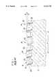
- FIG. 1is a fragmentary, cross-sectional view of an as-cut wafer 12 sliced in accordance with the prior art.
- the back and forth cutting action of the wire sawcauses wire marks, indicated generally at reference character 14, on a surface 16 of the wafer 12.
- the spacing between the wire marks 14is a function of the back and forth cycle time and the speed of relative motion between the ingot being sliced and the wire. Typically, this spacing is on the order of about 1/3 mm (approximately 387 ⁇ m in FIG. 1).
- the spacing between wire marks 14is indicated by reference character T shown between high spots 20 on the surface 16 of wafer 12.
- the depth of marks 14depends not only on the back and forth cycle time of the wire saw but also the size of the abrasive in the wire saw slurry. In FIG. 1, the depth D of wire marks 14 relative to the high spots 20 is about 24 ⁇ m.
- FIG. 1also illustrates a series of laser-scribed marks 22, which form part of an identification marking on the surface 16 of wafer 12.
- each mark 22has a generally cylindrical wall and a generally hemispherical bottom and appears as a dot when viewed from above.
- Conventional marking techniquesinclude marking the surface 16 of wafer 12 with an identifying code formed in an 8 ⁇ 32 grid of dots (often referred to as a T7 marking) (see FIG. 2).
- wafer 12is usually marked with an alphanumeric identifier (often referred to as an M12 marking) (see FIG. 2), which is also made up of a series of laser-scribed marks 22.
- each as-cut wafer 12undergoes a number of processing operations to shape it, reduce its thickness, remove damage caused by the slicing operation, and to create a highly reflective surface.
- These post-slicing processestypically involve the removal of up to 50 ⁇ m or more of semiconductor material from the surface 16 of wafer 12.
- a line 24shows the position of an exemplary final polished surface of wafer 12.
- thickness variations in general, and wire marks 14 in particularmake it difficult to meet customer specifications for dot depth and diameter on the final polished wafer when the initial marks are placed on an as-cut surface, such as surface 16.
- Exemplary laser marking specificationscall for dots having a depth of 45 ⁇ m ⁇ 15 ⁇ m and a diameter of 85 ⁇ m ⁇ 15 ⁇ m.
- a laser apparatusscribes marks 22 into the surface 16 of wafer 12 at a depth of about 100 ⁇ m. After removal of material in the post-slicing operations, the depth and/or diameter of the laser markings may or may not fall within the customer specifications for finished wafers.
- FIG. 1shows that the depths of marks 22 relative to the line 24 may vary significantly from one mark to another.
- the inventionmeets the above needs and overcomes the deficiencies of the prior art by providing improved methods of slicing wafers from ingots of semiconductor material.
- slicing wafersfrom ingots of semiconductor material.
- the provision of such methodsthat reduce thickness variations in certain regions of the wafers; the provision of such methods that provide improved accuracy and control of laser-scribed identification markings on the wafers; the provision of such methods that permit hard marking as-cut wafers; and the provision of such methods that are economically feasible and commercially practical.
- a method embodying aspects of the inventionincludes the step of defining an identification region of each wafer to be sliced from an ingot of semiconductor material using a wire saw.
- the wire sawincludes a wire that is movable in a forward direction and a reverse direction for slicing the ingot.
- the identification region of the waferis adapted for marking with an identification mark after slicing.
- the methodalso includes the step of slicing the ingot into wafers with the wire saw.
- the slicing stepincludes moving the wire in the forward and reverse directions during slicing except when slicing in the identification region of each wafer and moving the wire only in the forward direction when slicing in the identification region of each wafer. In slicing the ingot into wafers, thickness variations relative to the size of the identification mark are reduced in the identification region.
- Another embodiment of the inventionis directed to a method of slicing ingots of semiconductor material into wafers using a wire saw.
- the ingotseach include an outer surface having an alignment feature.
- the wire sawincludes a wire that is movable in a forward direction and a reverse direction for slicing the ingots.
- the methodincludes the steps of aligning the alignment features of the ingots in approximately the same position relative to the wire saw for each of the ingots and slicing each ingot into wafers with the wire saw.
- the slicing stepincludes moving the wire in the forward and reverse directions when slicing in a first region of each wafer and moving the wire only in the forward direction when slicing in a second region of each wafer. In slicing the ingots into wafers, thickness variations are reduced in the second region.
- the inventionmay comprise various other methods and systems.
- FIG. 1is a fragmentary cross section of a wafer sliced from an ingot using a wire saw according to the prior art.
- FIG. 2is a fragmentary top view of the wafer of FIG. 1.
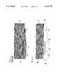
- FIG. 3is a fragmentary cross section of an exemplary wafer sliced from an ingot using a wire saw according to a preferred embodiment of the invention.
- FIG. 4is a fragmentary top view of the wafer of FIG. 3.
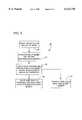
- FIG. 5is a flow diagram illustrating a method of slicing wafers for laser marking according to a preferred embodiment of the invention.
- an as-cut wafer 28 of semiconductor materialthat embodies aspects of the present invention has a surface 30 with an identification region 32 (see FIG. 4).
- the identification region 32is substantially free of thickness variations due to wire marks 14 and is adapted for laser-scribing with an identification marking.
- FIG. 3also illustrates the series of laser-scribed marks 22, which form part of the identification marking on the surface 30 of wafer 28.
- Line 24again shows the position of an exemplary final polished surface of wafer 28 after post-slicing processes remove semiconductor material from the surface 30 of wafer 28.
- the depths of marks 22 relative to line 24do not vary significantly from one mark to another even after removal of material in the post-slicing operations.
- the wafer 28, preferably sliced from an ingot of single crystal silicon,may have any diameter and target thickness that is appropriate for a semiconductor application.
- the diameter of wafer 28is from about 100 mm to about 300 mm or greater and its thickness is about 475 ⁇ m to about 900 ⁇ m or greater.
- the desired wafer thicknessincreases with increasing wafer diameter.
- wafer 28may have any crystal orientation, most semiconductor applications use a ⁇ 100> or ⁇ 111> crystal orientation.
- an exemplary T7 grid marking and an exemplary M12 alphanumeric identifierare laser-scribed into wafer surface 30 at the identification region 32.
- identification region 32is situated at the periphery of wafer 28 near a notch 36 in the outer edge of wafer 28.
- the notch 36provides a reference for defining identification region 32.
- an alignment feature on the outer surface of the ingotsuch as notch 36, for identifying crystal orientation, for example.
- Another known alignment featureis a facet ground into the outer surface of the ingot.
- a flow diagram 40illustrates a method of slicing an ingot of semiconductor material into wafers according to a preferred embodiment of the present invention.
- an operatordefines identification region 32 for the wafers to be sliced from the ingot.
- Identification region 32for example, provides an area for laser marking wafer 28 adjacent notch 36.
- the operatorpositions the ingot for slicing relative to the wire saw based on the defined identification region 32.
- the operatormounts notch 36 in the same location for each ingot, preferably in a start cut position that is straight down when the ingot is in the wire saw. In other words, the operator preferably positions notch 36, or another alignment feature on the ingot, downwardly relative to the direction of cutting.
- the wire sawbegins slicing the ingot into wafers at step 48 by moving its wire in a back and forth motion as the wire saw and ingot feed relatively toward each other along a linear feed path. This forces the wire and the ingot together during slicing.
- the wire sawhas, for example, a slurry mixture density of about 1.63 g/cc to about 1.65 g/cc, a wire speed of about 10 m/sec to about 15 m/sec, a total cycle length of approximately 500 meters and a back/forth ratio of approximately 2:3.
- the wire sawcontinues moving the wire back and forth during slicing of a first region of wafer 28 until the saw reaches a second region, namely, identification region 32.
- the wire sawchanges its cutting at step 50 to move the wire only in the forward direction rather than in a back and forth motion. Slicing in this manner reduces thickness variations in wafer 28 relative to the size of the laser-scribed identification marks 22 by eliminating wire marks 14 in the surface 30 of wafer 28 in identification region 32.
- advancing the wire during slicinguses more wire per amount of ingot cut than would otherwise be used during conventional back and forth slicing.
- identification region 32is defined to be near the periphery of wafer 28 adjacent notch 36 and by positioning the ingot with notch 36 in a downward position relative to the direction of cutting. This ensures that almost the entire diameter of the ingot is sliced with a back and forth wire motion before reaching identification region 32.
- identification markingsare wider than they are tall (e.g., a string of alphanumeric characters).
- the operatorpreferably defines identification region 32 to be situated generally horizontally and having a width and height that are greater or equal to the width and height of the laser marking.
- the wire sawincludes a plurality of guides for arranging its wire in a plurality of substantially parallel, regularly spaced lines.
- the guidesdefine wire guide pitch (i.e., the spacing between the adjacent portions of the wire).
- the method of FIG. 5provides for controlling wire guide pitch.
- the wire guide pitch control of step 52is performed during the preparation of the wire guide for installation on a wire saw. This control involves eliminating machining errors and accurately accounting for wire wear to reduce thickness variations in the as-cut wafers.
- Step 52also includes controlling the density of the abrasive slurry in the contact area between the wire and the ingot by using a statistical process control.
- a statistical process controlIn general, newer slurry is less dense and leads to the production of thinner wafers with greater total thickness variation whereas older slurry is more dense and leads to the production of thicker wafers with lesser total thickness variation. For this reason, consistent slurry density is desired.
- Conventional slurry controlinvolves an open loop process of replacing a portion of the total volume of slurry between slicing runs. The amount of slurry replaced is a function of the size of the ingot most recently sliced.
- the method of the present inventioncontemplates a closed loop process for controlling thickness variations by maintaining slurry density relatively constant from one slicing run to the next.
Landscapes
- Engineering & Computer Science (AREA)
- Mechanical Engineering (AREA)
- Physics & Mathematics (AREA)
- Condensed Matter Physics & Semiconductors (AREA)
- General Physics & Mathematics (AREA)
- Computer Hardware Design (AREA)
- Microelectronics & Electronic Packaging (AREA)
- Power Engineering (AREA)
- Mechanical Treatment Of Semiconductor (AREA)
Abstract
Description
Claims (14)
Priority Applications (1)
| Application Number | Priority Date | Filing Date | Title |
|---|---|---|---|
| US09/285,337US6112738A (en) | 1999-04-02 | 1999-04-02 | Method of slicing silicon wafers for laser marking |
Applications Claiming Priority (1)
| Application Number | Priority Date | Filing Date | Title |
|---|---|---|---|
| US09/285,337US6112738A (en) | 1999-04-02 | 1999-04-02 | Method of slicing silicon wafers for laser marking |
Publications (1)
| Publication Number | Publication Date |
|---|---|
| US6112738Atrue US6112738A (en) | 2000-09-05 |
Family
ID=23093792
Family Applications (1)
| Application Number | Title | Priority Date | Filing Date |
|---|---|---|---|
| US09/285,337Expired - Fee RelatedUS6112738A (en) | 1999-04-02 | 1999-04-02 | Method of slicing silicon wafers for laser marking |
Country Status (1)
| Country | Link |
|---|---|
| US (1) | US6112738A (en) |
Cited By (12)
| Publication number | Priority date | Publication date | Assignee | Title |
|---|---|---|---|---|
| US6420792B1 (en)* | 1999-09-24 | 2002-07-16 | Texas Instruments Incorporated | Semiconductor wafer edge marking |
| US6482661B1 (en)* | 2000-03-09 | 2002-11-19 | Intergen, Inc. | Method of tracking wafers from ingot |
| EP1717001A1 (en)* | 2005-04-25 | 2006-11-02 | Nippei Toyama Corporation | Method for manufacturing semiconductor wafers, method for their slicing and wire saw used for the same |
| US20080041159A1 (en)* | 2006-06-22 | 2008-02-21 | Siltronic Ag | Method and Appartus For Detection Of Mechanical Defects In An Ingot Piece Composed Of Semiconductor Material |
| WO2008151649A1 (en) | 2007-06-13 | 2008-12-18 | Conergy Ag | Method for marking wafers |
| US20090050198A1 (en)* | 2006-02-28 | 2009-02-26 | Joerg Mueller | Solar-Cell Marking Method and Solar Cell |
| US20100300259A1 (en)* | 2009-05-29 | 2010-12-02 | Applied Materials, Inc. | Substrate side marking and identification |
| US20110011838A1 (en)* | 2009-07-16 | 2011-01-20 | Shu-Ling Kuo | Method for fabricating semicoductor wafers applicable to integrated circuit manufacture |
| US20130174829A1 (en)* | 2011-12-29 | 2013-07-11 | Memc Electronic Materials, Inc. | Methods For Mounting An Ingot On A Wire Saw |
| CN103419290A (en)* | 2012-05-23 | 2013-12-04 | 浙江锦锋光伏科技有限公司 | Tool feeding method for multi-wire sawing of silicon wafers |
| US9099481B2 (en) | 2013-03-15 | 2015-08-04 | Semiconductor Components Industries, Llc | Methods of laser marking semiconductor substrates |
| CN114161596A (en)* | 2021-12-23 | 2022-03-11 | 西安奕斯伟材料科技有限公司 | System and method for producing silicon wafer and single crystal silicon rod |
Citations (11)
| Publication number | Priority date | Publication date | Assignee | Title |
|---|---|---|---|---|
| US5269285A (en)* | 1991-11-29 | 1993-12-14 | Shin-Etsu Handotai Company, Ltd. | Wire saw and slicing method using the same |
| EP0755751A1 (en)* | 1995-07-28 | 1997-01-29 | Shin-Etsu Handotai Co., Ltd. | Method of manufacturing semiconductor wafers and process of and apparatus for grinding used for the same method of manufacture |
| US5610104A (en)* | 1996-05-21 | 1997-03-11 | Cypress Semiconductor Corporation | Method of providing a mark for identification on a silicon surface |
| EP0798405A2 (en)* | 1996-03-25 | 1997-10-01 | Shin-Etsu Handotai Co., Ltd. | Method of manufacturing semiconductor wafers |
| US5715806A (en)* | 1994-12-15 | 1998-02-10 | Sharp Kabushiki Kaisha | Multi-wire saw device for slicing a semi-conductor ingot into wafers with a cassette for housing wafers sliced therefrom, and slicing method using the same |
| US5735258A (en)* | 1995-09-22 | 1998-04-07 | Memc Electronic Materials, Inc. | Cutting machine |
| US5810643A (en)* | 1995-06-22 | 1998-09-22 | Shin-Etsu Handotai Co., Ltd. | Wire saw cutting method synchronizing workpiece feed speed with wire speed |
| US5875769A (en)* | 1996-03-29 | 1999-03-02 | Shin-Etsu Handotai Co., Ltd. | Method of slicing semiconductor single crystal ingot |
| US5875770A (en)* | 1996-04-22 | 1999-03-02 | Komatsu Electronic Metals Co., Ltd. | Method of cutting semiconductor ingots and apparatus for cutting thereof |
| US5931147A (en)* | 1996-03-27 | 1999-08-03 | Shin-Etsu Handotai Co., Ltd. | Method of cutting a workpiece with a wire saw |
| US5937844A (en)* | 1996-03-26 | 1999-08-17 | Shin-Etsu Handotai Co., Ltd. | Method for slicing cylindrical workpieces by varying slurry conditions and wire feed rate during slicing |
- 1999
- 1999-04-02USUS09/285,337patent/US6112738A/ennot_activeExpired - Fee Related
Patent Citations (11)
| Publication number | Priority date | Publication date | Assignee | Title |
|---|---|---|---|---|
| US5269285A (en)* | 1991-11-29 | 1993-12-14 | Shin-Etsu Handotai Company, Ltd. | Wire saw and slicing method using the same |
| US5715806A (en)* | 1994-12-15 | 1998-02-10 | Sharp Kabushiki Kaisha | Multi-wire saw device for slicing a semi-conductor ingot into wafers with a cassette for housing wafers sliced therefrom, and slicing method using the same |
| US5810643A (en)* | 1995-06-22 | 1998-09-22 | Shin-Etsu Handotai Co., Ltd. | Wire saw cutting method synchronizing workpiece feed speed with wire speed |
| EP0755751A1 (en)* | 1995-07-28 | 1997-01-29 | Shin-Etsu Handotai Co., Ltd. | Method of manufacturing semiconductor wafers and process of and apparatus for grinding used for the same method of manufacture |
| US5735258A (en)* | 1995-09-22 | 1998-04-07 | Memc Electronic Materials, Inc. | Cutting machine |
| EP0798405A2 (en)* | 1996-03-25 | 1997-10-01 | Shin-Etsu Handotai Co., Ltd. | Method of manufacturing semiconductor wafers |
| US5937844A (en)* | 1996-03-26 | 1999-08-17 | Shin-Etsu Handotai Co., Ltd. | Method for slicing cylindrical workpieces by varying slurry conditions and wire feed rate during slicing |
| US5931147A (en)* | 1996-03-27 | 1999-08-03 | Shin-Etsu Handotai Co., Ltd. | Method of cutting a workpiece with a wire saw |
| US5875769A (en)* | 1996-03-29 | 1999-03-02 | Shin-Etsu Handotai Co., Ltd. | Method of slicing semiconductor single crystal ingot |
| US5875770A (en)* | 1996-04-22 | 1999-03-02 | Komatsu Electronic Metals Co., Ltd. | Method of cutting semiconductor ingots and apparatus for cutting thereof |
| US5610104A (en)* | 1996-05-21 | 1997-03-11 | Cypress Semiconductor Corporation | Method of providing a mark for identification on a silicon surface |
Cited By (18)
| Publication number | Priority date | Publication date | Assignee | Title |
|---|---|---|---|---|
| US6710364B2 (en) | 1999-09-24 | 2004-03-23 | Texas Instruments Incorporated | Semiconductor wafer edge marking |
| US6420792B1 (en)* | 1999-09-24 | 2002-07-16 | Texas Instruments Incorporated | Semiconductor wafer edge marking |
| US6482661B1 (en)* | 2000-03-09 | 2002-11-19 | Intergen, Inc. | Method of tracking wafers from ingot |
| EP1717001A1 (en)* | 2005-04-25 | 2006-11-02 | Nippei Toyama Corporation | Method for manufacturing semiconductor wafers, method for their slicing and wire saw used for the same |
| US8492240B2 (en) | 2006-02-28 | 2013-07-23 | Hanwha Q.CELLS GmbH | Solar-cell marking method and solar cell |
| US20090050198A1 (en)* | 2006-02-28 | 2009-02-26 | Joerg Mueller | Solar-Cell Marking Method and Solar Cell |
| US20080041159A1 (en)* | 2006-06-22 | 2008-02-21 | Siltronic Ag | Method and Appartus For Detection Of Mechanical Defects In An Ingot Piece Composed Of Semiconductor Material |
| US8038895B2 (en)* | 2006-06-22 | 2011-10-18 | Siltronic Ag | Method and appartus for detection of mechanical defects in an ingot piece composed of semiconductor material |
| WO2008151649A1 (en) | 2007-06-13 | 2008-12-18 | Conergy Ag | Method for marking wafers |
| US20100300259A1 (en)* | 2009-05-29 | 2010-12-02 | Applied Materials, Inc. | Substrate side marking and identification |
| US20110011838A1 (en)* | 2009-07-16 | 2011-01-20 | Shu-Ling Kuo | Method for fabricating semicoductor wafers applicable to integrated circuit manufacture |
| US20130174829A1 (en)* | 2011-12-29 | 2013-07-11 | Memc Electronic Materials, Inc. | Methods For Mounting An Ingot On A Wire Saw |
| US9156187B2 (en)* | 2011-12-29 | 2015-10-13 | Sunedison Semiconductor Ltd. | Methods for mounting an ingot on a wire saw |
| CN103419290A (en)* | 2012-05-23 | 2013-12-04 | 浙江锦锋光伏科技有限公司 | Tool feeding method for multi-wire sawing of silicon wafers |
| US9099481B2 (en) | 2013-03-15 | 2015-08-04 | Semiconductor Components Industries, Llc | Methods of laser marking semiconductor substrates |
| US9355965B2 (en) | 2013-03-15 | 2016-05-31 | Semiconductor Components Industries, Llc | Semiconductor devices and methods of making the same |
| CN114161596A (en)* | 2021-12-23 | 2022-03-11 | 西安奕斯伟材料科技有限公司 | System and method for producing silicon wafer and single crystal silicon rod |
| CN114161596B (en)* | 2021-12-23 | 2024-04-09 | 西安奕斯伟材料科技股份有限公司 | System and method for producing silicon wafer and monocrystalline silicon rod |
Similar Documents
| Publication | Publication Date | Title |
|---|---|---|
| US6112738A (en) | Method of slicing silicon wafers for laser marking | |
| US4227348A (en) | Method of slicing a wafer | |
| JP4525353B2 (en) | Method for manufacturing group III nitride substrate | |
| CN101618519B (en) | Method and device thereof for linearly cutting silicon slice | |
| KR100624931B1 (en) | Dividing Method of Semiconductor Wafer | |
| KR102028765B1 (en) | Method for dividing circular plate-like object | |
| US20090057841A1 (en) | Wafer | |
| CN112720885A (en) | Crystal bar slotting method and crystal bar slotting device | |
| EP0798090A2 (en) | Method of cutting a workpiece with a wire saw | |
| CN102266973B (en) | Machining method for milling two curved surfaces of tapered honeycomb variable-thickness structural part | |
| EP1264648A1 (en) | Method of bending and cutting a metal strip | |
| US6797585B1 (en) | Nonintrusive wafer marking | |
| GB2143849A (en) | Electrolytic precision drilling | |
| JP2003159642A (en) | Work cutting method and multi-wire saw system | |
| US6903304B1 (en) | Process for dressing molded array package saw blade | |
| US4287256A (en) | Wafer and boule protection during the blade return stroke of a wafer saw | |
| DE102023200832A1 (en) | WAFER MANUFACTURING PROCESS | |
| KR101751648B1 (en) | Flat bed type cutting device with multi-gantry | |
| US4449909A (en) | Die-cut brick machine for special brick shapes | |
| US6367467B1 (en) | Holding unit for semiconductor wafer sawing | |
| US4326494A (en) | Wafer and boule protection during the blade return stroke of a wafer saw | |
| KR102412482B1 (en) | Machining method | |
| JP3305954B2 (en) | Gate cut mechanism for molded products | |
| Zainuddin | An introduction of strip chopping cut method to establish a robust strip based dicing process on tape dicing concept | |
| JP3346603B2 (en) | Lead frame side burr removal mechanism |
Legal Events
| Date | Code | Title | Description |
|---|---|---|---|
| AS | Assignment | Owner name:MEMC ELECTRONIC MATERIALS, INC., MISSOURI Free format text:ASSIGNMENT OF ASSIGNORS INTEREST;ASSIGNORS:WITTE, DALE A.;RAGAN, TRACY;REEL/FRAME:009881/0077 Effective date:19990330 | |
| AS | Assignment | Owner name:MEMC ELECTRONIC MATERIALS, INC., MISSOURI Free format text:TERMINATION OF SECURITY INTEREST;ASSIGNOR:E.ON AG;REEL/FRAME:012263/0944 Effective date:20011113 Owner name:CITICORP USA, INC., DELAWARE Free format text:SECURITY INTEREST;ASSIGNORS:MEMC PASADENA, INC.;PLASMASIL, L.L.C.;SIBOND, L.L.C.;AND OTHERS;REEL/FRAME:012273/0145 Effective date:20011113 Owner name:CITICORP USA, INC., DELAWARE Free format text:SECURITY AGREEMENT;ASSIGNORS:MEMC PASADENA, INC.;PLASMASIL, L.L.C.;SIBOND, L.L.C.;AND OTHERS;REEL/FRAME:012280/0161 Effective date:20011113 | |
| AS | Assignment | Owner name:E. ON AG, GERMANY Free format text:SECURITY INTEREST;ASSIGNOR:MEMC ELECTRONIC MATERIALS, INC.;REEL/FRAME:012407/0806 Effective date:20011025 | |
| AS | Assignment | Owner name:CITICORP USA, INC., DELAWARE Free format text:SECURITY AGREEMENT;ASSIGNORS:MEMC PASADENA, INC.;PLASMASIL, L.L.C.;SIBOND, L.L.C.;AND OTHERS;REEL/FRAME:012365/0345 Effective date:20011221 | |
| AS | Assignment | Owner name:CITICORP USA, INC., DELAWARE Free format text:SECURITY AGREEMENT;ASSIGNORS:MEMC ELECTRONIC MATERIALS, INC.;MEMC PASADENA, INC.;PLASMASIL, L.L.C.;AND OTHERS;REEL/FRAME:013964/0378;SIGNING DATES FROM 20020303 TO 20030303 Owner name:CITICORP USA, INC., DELAWARE Free format text:SECURITY AGREEMENT;ASSIGNORS:MEMC ELECTRONIC MATERIALS, INC.;MEMC PASADENA, INC.;PLASMASIL, L.L.C.;AND OTHERS;SIGNING DATES FROM 20020303 TO 20030303;REEL/FRAME:013964/0378 | |
| REMI | Maintenance fee reminder mailed | ||
| LAPS | Lapse for failure to pay maintenance fees | ||
| FP | Lapsed due to failure to pay maintenance fee | Effective date:20040905 | |
| AS | Assignment | Owner name:MEMC ELECTRONIC MATERIALS, INC., MISSOURI Free format text:RELEASE OF SECURITY INTEREST;ASSIGNOR:CITICORP USA, INC.;REEL/FRAME:016641/0045 Effective date:20050602 | |
| AS | Assignment | Owner name:SIBOND, L.L.C., MISSOURI Free format text:RELEASE OF SECURITY INTEREST TO REEL/FRAME: 012280/0161;ASSIGNOR:CITICORP USA, INC.;REEL/FRAME:032458/0794 Effective date:20140313 Owner name:PLASMASIL, L.L.C., MISSOURI Free format text:RELEASE OF SECURITY INTEREST TO REEL/FRAME: 012280/0161;ASSIGNOR:CITICORP USA, INC.;REEL/FRAME:032458/0794 Effective date:20140313 Owner name:MEMC PASADENA, INC., TEXAS Free format text:RELEASE OF SECURITY INTEREST TO REEL/FRAME: 012280/0161;ASSIGNOR:CITICORP USA, INC.;REEL/FRAME:032458/0794 Effective date:20140313 Owner name:MEMC INTERNATIONAL, INC. (NOW KNOWN AS SUNEDISON I Free format text:RELEASE OF SECURITY INTEREST TO REEL/FRAME: 012280/0161;ASSIGNOR:CITICORP USA, INC.;REEL/FRAME:032458/0794 Effective date:20140313 Owner name:MEMC ELECTRONIC MATERIALS, INC. (NOW KNOWN AS SUNE Free format text:RELEASE OF SECURITY INTEREST TO REEL/FRAME: 012280/0161;ASSIGNOR:CITICORP USA, INC.;REEL/FRAME:032458/0794 Effective date:20140313 Owner name:MEMC SOUTHWEST INC., MISSOURI Free format text:RELEASE OF SECURITY INTEREST TO REEL/FRAME: 012280/0161;ASSIGNOR:CITICORP USA, INC.;REEL/FRAME:032458/0794 Effective date:20140313 | |
| STCH | Information on status: patent discontinuation | Free format text:PATENT EXPIRED DUE TO NONPAYMENT OF MAINTENANCE FEES UNDER 37 CFR 1.362 |