US6111424A - Testing method and apparatus for flat panel displays using infrared imaging - Google Patents
Testing method and apparatus for flat panel displays using infrared imagingDownload PDFInfo
- Publication number
- US6111424A US6111424AUS08/923,507US92350797AUS6111424AUS 6111424 AUS6111424 AUS 6111424AUS 92350797 AUS92350797 AUS 92350797AUS 6111424 AUS6111424 AUS 6111424A
- Authority
- US
- United States
- Prior art keywords
- active plate
- pixels
- image
- plate
- testing
- Prior art date
- Legal status (The legal status is an assumption and is not a legal conclusion. Google has not performed a legal analysis and makes no representation as to the accuracy of the status listed.)
- Expired - Lifetime
Links
- 238000012360testing methodMethods0.000titleclaimsabstractdescription28
- 238000003331infrared imagingMethods0.000title1
- 238000000034methodMethods0.000claimsabstractdescription75
- 230000008569processEffects0.000claimsabstractdescription31
- 230000007547defectEffects0.000claimsabstractdescription29
- 238000010438heat treatmentMethods0.000claimsabstractdescription21
- 230000004044responseEffects0.000claimsabstractdescription18
- 230000002950deficientEffects0.000claimsabstractdescription17
- 238000004519manufacturing processMethods0.000claimsabstractdescription13
- 239000000758substrateSubstances0.000claimsdescription4
- 238000010998test methodMethods0.000claims3
- 238000001514detection methodMethods0.000abstractdescription7
- 239000004973liquid crystal related substanceSubstances0.000abstractdescription7
- 238000001931thermographyMethods0.000abstractdescription5
- 238000010191image analysisMethods0.000description9
- 238000013500data storageMethods0.000description6
- 238000013339in-process testingMethods0.000description6
- 238000010586diagramMethods0.000description5
- 239000011159matrix materialSubstances0.000description5
- 238000002405diagnostic procedureMethods0.000description4
- 238000003384imaging methodMethods0.000description4
- 230000005684electric fieldEffects0.000description3
- 230000008439repair processEffects0.000description3
- 239000000523sampleSubstances0.000description3
- 239000010409thin filmSubstances0.000description3
- 238000012935AveragingMethods0.000description2
- 230000001419dependent effectEffects0.000description2
- 238000007689inspectionMethods0.000description2
- 239000000463materialSubstances0.000description2
- 230000005055memory storageEffects0.000description2
- 230000035945sensitivityEffects0.000description2
- 230000003213activating effectEffects0.000description1
- 230000002547anomalous effectEffects0.000description1
- 238000013459approachMethods0.000description1
- 239000003990capacitorSubstances0.000description1
- 230000001351cycling effectEffects0.000description1
- 230000007812deficiencyEffects0.000description1
- 239000000428dustSubstances0.000description1
- 238000005516engineering processMethods0.000description1
- 230000001747exhibiting effectEffects0.000description1
- 230000006870functionEffects0.000description1
- 230000004807localizationEffects0.000description1
- 239000011859microparticleSubstances0.000description1
- 238000012986modificationMethods0.000description1
- 230000004048modificationEffects0.000description1
- 239000012811non-conductive materialSubstances0.000description1
- 238000011179visual inspectionMethods0.000description1
Images


Classifications
- G—PHYSICS
- G09—EDUCATION; CRYPTOGRAPHY; DISPLAY; ADVERTISING; SEALS
- G09G—ARRANGEMENTS OR CIRCUITS FOR CONTROL OF INDICATING DEVICES USING STATIC MEANS TO PRESENT VARIABLE INFORMATION
- G09G3/00—Control arrangements or circuits, of interest only in connection with visual indicators other than cathode-ray tubes
- G09G3/006—Electronic inspection or testing of displays and display drivers, e.g. of LED or LCD displays
- G—PHYSICS
- G01—MEASURING; TESTING
- G01R—MEASURING ELECTRIC VARIABLES; MEASURING MAGNETIC VARIABLES
- G01R31/00—Arrangements for testing electric properties; Arrangements for locating electric faults; Arrangements for electrical testing characterised by what is being tested not provided for elsewhere
- G01R31/28—Testing of electronic circuits, e.g. by signal tracer
- G01R31/302—Contactless testing
- G01R31/308—Contactless testing using non-ionising electromagnetic radiation, e.g. optical radiation
Definitions
- the present inventionrelates generally to a method and apparatus for testing of flat panel displays, and more particularly, to an in-process method and apparatus for testing an active plate of a flat panel display.
- Liquid crystal and other flat panel displaysare increasingly being utilized for various applications, from color televisions and computer monitors to roadside signs. Such devices are typically fabricated utilizing well-known clean room fabrication techniques. Nonetheless, dust, other micro-particles and other factors often lead to defects, such as open circuits or short circuits, in the increasingly high-density environment of an active matrix liquid crystal display. The poor manufacturing yields, which may be as low as ten percent (10%), as well as the time and expense required to test such devices, have greatly contributed to the fabrication costs associated with such devices.
- in-process voltage imaging techniquessuch as those developed by Photo Dynamics, Inc., and described, for example, in U.S. Pat. No. 5,570,011 to Henley, entitled “Method For Testing a Device Using Voltage Imaging,” utilize an electro-optical probe to image the electric field at a pixel.
- the electro-optical probehas a narrow field of view and must be positioned a short distance from the plate.
- a time-consuming step-and-repeat approachmust be implemented to image an entire active plate.
- PCBsprinted circuit boards
- IR thermography techniquesdetect the IR emission of the circuit being tested when an electric signal is applied and compare the heating response characteristics to a known defect-free sample.
- U.S. Pat. No. 3,991,302 to Dannerentitled “Method For Detecting and Isolating Faults in Digital and Analog Circuits With Multiple Infrared Scanning Under Conditions of Different Stimuli,” for example, discloses a method for detecting faults in circuits based on infrared heating response characteristics.
- an in-process method and apparatustests an active plate of a flat panel display.
- the flat panel displaymay be an active matrix liquid crystal display (AMLCD) or any other device where an electric field is applied to an array of uniform pixels to control transparency or emission of light and where electrical energy is dissipated on a resistive structure.
- the display testing apparatuspreferably utilizes an infrared thermal analyzer including an infrared (IR) camera and an image analyzer, for recording and analyzing heating response characteristics of the active plate upon application of an appropriate electric signal.
- the electric voltage applied to the active platecan be an AC signal, a DC signal or a pulsed signal.
- an active plate for use with a flat panel display deviceis tested during the fabrication process using IR thermography techniques.
- the active plateis tested by evaluating the IR emission of the active plate when an electric voltage is applied to shorting bars of the active plate, to uniformly power the array of pixels in the active plate.
- the testing technique of the present inventionexhibits minimal invasiveness, as only the shorting bars of the active plate are electrically accessed.
- the active plateconsists of an array of uniform pixels.
- pixels having identical electrical characteristicsshould heat up in a uniform manner over time, as each pixel reaches a stable operating temperature.
- the heating response characteristics of the active plateare preferably evaluated after the active plate reaches a stable operating temperature.
- the dynamics of the heating response characteristics of the active platesuch as the rate of heating, may be evaluated to indicate defects in the active plate.
- each pixel in the arrayheats up uniformly, and upon detection by an infrared camera, a uniform IR image is obtained across the plate. If there are defects in the active plate, however, such as one or more open lines, short circuits, or other non-uniform electric parameters, the various pixels in the active plate do not heat up uniformly and will reach different operating temperatures. Thus, the defective active plate dissipates IR energy in a non-uniform manner, and upon detection by an infrared camera, a non-uniform image of the active plate is obtained, providing a map of any defects on the plate. In the presence of defects, the infrared camera records an image of the active plate having bright spots and dark spots, relative to an expected uniform image intensity, corresponding to defective regions of the active plate.
- the final operating temperature of each pixel, upon application of a particular electric signalis detected.
- the heating dynamics of the active platecan be time-resolved as the pixels of the active plate heat up in response to an applied electric signal.
- the reliability of an active platecan be evaluated by applying a voltage having a higher magnitude than the typical operating voltage of the flat panel display device.
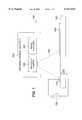
- FIG. 1is a schematic block diagram illustrating a display testing apparatus in accordance with one embodiment of the present invention
- FIG. 2ashows an illustrative active plate having a plurality of pixels, to be tested by the display testing apparatus of FIG. 1;
- FIG. 2bshows an illustrative schematic diagram of a typical pixel of FIG. 2a
- FIG. 3is a schematic block diagram of an exemplary infrared thermal analyzer of FIG. 1;
- FIG. 4is a flow chart describing an exemplary image capture process as implemented by the infrared thermal analyzer of FIG. 3;
- FIG. 5is a flow chart describing an exemplary image analysis process as implemented by the infrared thermal analyzer of FIG. 3;
- FIG. 6is a flow chart describing an exemplary plate diagnostic subroutine as implemented by the infrared thermal analyzer of FIG. 3.
- FIG. 1is a schematic block diagram illustrating the components of a display testing apparatus 100 incorporating features of the present invention, for testing an active plate 200, discussed further below in conjunction with FIG. 2a, of a flat panel display device, such as an active matrix liquid crystal display (AMLCD) (not shown), or any other device where an electric field is applied to an array of uniform pixels to control transparency or emission of light and where electrical energy is dissipated on a resistive structure, such as a plasma display.
- the display testing apparatus 100includes an infrared (IR) camera 310 and an image analyzer 320, for respectively recording and analyzing heating response characteristics of the active plate 200 upon application of an appropriate electric signal.
- IRinfrared
- the infrared camera 310 and the image analyzer 320may be embodied as separate units or as part of a single integrated device, such as an infrared thermal analyzer 300, discussed further below in conjunction with FIG. 3.
- the active plate 200is preferably positioned on a suitable holding plate 130 during testing.
- an illustrative active plate 200 for use with a flat panel display deviceis tested during the fabrication process using IR thermography techniques.
- an "active plate”refers to an array of thin-film transistors (TFTs), or other circuitry for selectively addressing individual pixels of an array, deposited on a substrate or other non-conductive material.
- TFTsthin-film transistors
- an active plate 200is tested by evaluating the IR emission of the active plate 200 when an electric voltage, produced by a voltage source 150, is applied to shorting bars 210, 220 on the active plate 200, to uniformly power the array of pixels 230 in the active plate 200.
- the shorting bars 210, 220connect the gate and data lines 240, 250 of the active plate 200.
- the testing technique of the present inventionexhibits minimal invasiveness, as only the shorting bars 210, 220 of the active plate 200 are electrically accessed.
- the shorting bars 210, 220are provided during the fabrication process to prevent damage to the active plate 200 due to electro-static discharge (ESD).
- ESDelectro-static discharge
- the shorting bars 210, 220are typically removed from the active plate 200 before final assembly of the flat panel display, once the risk of ESD damage to the active plate 200 is reduced.
- the active plate 200typically consists of an array of uniform pixels, with each pixel including a thin-film transistor and a capacitor, as shown in FIG. 2b.
- each pixeloperates like a resistive-capacitive (RC) circuit, dissipating heat when the circuit is charged and discharged.
- RCresistive-capacitive
- the charge/discharge cycle of the actual operation of the active plate 200 being testedis simulated. If a single cycle provides the minimum dissipation required for being detected, a DC signal may be applied. In general, however, the cycle may have to be repeated, and depending on the characteristics of the device, an AC signal having an appropriate frequency is utilized. Generally, the higher the frequency, in accordance with the characteristics of the device, the shorter the time to reach the stable operating temperature.
- pixels having identical electrical characteristicsshould heat up in a uniform manner over time, as each pixel reaches a stable operating temperature.
- the heating response characteristics of the active plate 200are preferably evaluated after the active plate 200 dissipates sufficient heat to be detected by the infrared camera 310. It is noted that the lowest threshold depends on the electrical characteristics of each active plate 200 and the sensitivity of the infrared camera 310. In addition, as discussed below, the heating response characteristics of the active plate 200 are preferably not evaluated until the active plate 200 reaches a stable operating temperature.
- the appropriate waiting periodis a function of the electrical characteristics of the pixel configuration, as would be apparent to a person of ordinary skill. In particular, the appropriate waiting time depends on the pixel characteristics and the modalities of power application. As indicated above, the waiting time may be shortened by increasing the frequency with which the power is applied, and then cleared.
- each pixel in the arrayheats up uniformly, and upon detection by an infrared camera 310, a uniform IR image is obtained across the plate 200. If there are defects in the active plate 200, however, such as one or more open lines, short circuits, or other non-uniform electric parameters, the various pixels in the active plate 200 do not heat up uniformly and will reach different operating temperatures. Thus, the defective active plate 200 dissipates IR energy in a non-uniform manner, and upon detection by an infrared camera 310, a non-uniform image of the active plate 200 is obtained, providing a map of any defects on the plate 200.
- the infrared camera 310records an image of the active plate 200 having bright spots and dark spots, relative to an expected uniform image intensity, corresponding to defective regions of the active plate 200. It is noted that the expected image intensity value can be obtained by averaging the pixel intensity values of a given image frame, or by means of a reference frame corresponding to an ideal or defect-free active plate 200. As discussed further below in conjunction with FIGS. 3 and 5, the image analyzer 320 evaluates the images produced by the infrared camera 310 and preferably localizes regions containing defective pixels.
- the heating response characteristics of the active plate 200are evaluated under varying voltage conditions.
- the final operating temperature of each pixelupon application of a particular electric signal, is detected.
- the heating dynamics of the active plate 200can be time-resolved as the pixels of the active plate 200 heat up in response to an applied electric signal.
- the identical pixels of an active plate 200should heat up in a uniform manner over time. Thus, any deviation in the heating response indicates a non-uniformity in the electrical characteristics of a given pixel.
- the reliability of an active plate 200can be evaluated by applying a voltage having a higher magnitude than the typical operating voltage of the flat panel display device. In this manner, devices exhibiting poor reliability can be identified and discarded. It is noted that the voltage applied to the active plate 200 by the image capture process 400, discussed further below in conjunction with FIG. 4, may be higher than the recommended operating voltage of the device, provided that the applied voltage does not damage the device, and thereby shorten the time required to reach a stable operating temperature. In this manner, the inspection of the active plate 200 for defects is combined with a reliability test.
- the electric voltage applied to the shorting bars 210, 220can be an AC signal, a DC signal or a pulsed signal.
- the frequency of an AC voltage signal, or a pulsed DC voltage signalthe charge/discharge cycling of the active plate 200 is varied, and the information obtained is further enriched.
- the pixels 230 of the active plate 200will heat up faster.
- FIG. 2ashows an illustrative active plate 200, having a plurality of pixels 230.
- a given pixelsuch as the pixel 270, may be selectively activated by application of an appropriate voltage to the respective data line 240 and gate line 250, which thereby activates an associated thin film transistor (TFT), such as the TFT 260 shown generally in FIG. 2a for pixel 270, and in greater detail in FIG. 2b.
- TFTthin film transistor
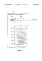
- FIG. 3is a block diagram showing the architecture of an illustrative infrared thermal analyzer 300.
- the infrared thermal analyzer 300may be embodied, for example, as a commercially available infrared thermal analyzer, such as those manufactured by AGEMA, Barnes and Inframetrics, as modified herein to evaluate the IR thermal dissipation of an active plate 200.
- the infrared thermal analyzer 300preferably consists of an infrared camera 310 and an image analyzer 320. The sensitivity and spatial resolution required by a given infrared camera 310 is determined by parameters of the active plate 200 to be tested.
- the field-of-view 140 of current commercially available infrared cameras 310is typically sufficient to image the entire area of an active plate 200, the available resolution typically provides detection of gross areas containing defects.
- a known step-and-repeat process of increasing resolutionis preferably utilized to focus in on regions containing anomalous luminosity to localize individual defective pixels.
- the infrared thermal analyzer 300preferably includes a processor 330 and related memory, such as a data storage device 340.
- the processor 330may be embodied as a single processor, or a number of processors operating in parallel.
- the data storage device 340 and/or a read only memory (ROM)are operable to store one or more instructions, which the processor 330 is operable to retrieve, interpret and execute.
- the processor 330preferably includes a control unit, an arithmetic logic unit (ALU), and a local memory storage device, such as, for example, an instruction cache or a plurality of registers, in a known manner.
- the control unitis operable to retrieve instructions from the data storage device 340 or ROM.
- the ALUis operable to perform a plurality of operations needed to carry out instructions.
- the local memory storage deviceis operable to provide high-speed storage used for storing temporary results and control information.
- the data storage device 340preferably contains an area of frame memory 350 for storing one or more images of one or more active plate 200 being evaluated.
- the data storage device 340preferably contains an area of reference frame memory 360 for optionally storing one or more reference frames corresponding to each active plate 200 configuration.
- the data storage device 340preferably also includes an image capture process 400, an image analysis process 500 and a plate diagnostic subroutine 600.
- the image capture process 400obtains one or more images of the active plate 200, preferably after the pixels 230 of the active plate 200 have reached a stable operating temperature.
- the image analysis process 500preferably analyzes the images obtained by the infrared camera 310 to identify regions of the active plate 200 having image intensity values that deviate from an expected or average image intensity value by more than a predefined tolerance.
- the plate diagnostic subroutine 600preferably further analyzes the regions identified by the image analysis process 500 at higher resolution to identify defective pixels and the potential source of defects in the fabrication process.
- Information obtained by the plate diagnostic subroutine 600may be utilized to repair a defective active plate 200, as would be apparent to a person of ordinary skill. It is noted that many commercially available infrared thermal analyzers 300, such as those identified above, provide software features incorporating features of the image capture process 400 and image analysis process 500 to study heating dynamics of a generic device being tested.
- the infrared thermal analyzer 300preferably executes an image capture process 400, shown in FIG. 4, to obtain one or more images of the active plate 200, preferably after the pixels 230 of the active plate 200 have reached a stable operating temperature.
- the image capture process 400begins the processes embodying the principles of the present invention during step 410 by applying an appropriate electric signal to the active plate 200 being tested. Thereafter, the image capture process 400 preferably waits a predefined period during step 420 until the pixels 230 of the active plate 200 heat up to a stable operating temperature. It is noted that in a time-resolved implementation, multiple images of the active plate 200 would be taken during step 420, as the pixels 230 of the active plate 200 heat up.
- the infrared camera 310then takes an image of the IR dissipation of the active plate 200 during step 430, using a step-and-repeat procedure, if necessary, and stores the obtained image in the frame memory 350 during step 440. Thereafter, program control terminates during step 450.
- the infrared thermal analyzer 300preferably executes an image analysis process 500, shown in FIG. 5, to analyze the images obtained by the infrared camera 310 and to identify regions of the active plate 200 having image intensity values that deviate from an expected or average image intensity value by more than a predefined tolerance.
- the image analysis process 500begins the processes embodying the principles of the present invention during step 510 by retrieving an image frame to be processed from the frame memory 350.
- the image analysis process 500then identifies the number of regions within the active plate 200 during step 520 that have intensity values deviating from an expected intensity value by more than a predefined tolerance. It is noted that the expected image intensity value and the predefined tolerance are dependent upon the electrical parameters of the active plate 200 being tested. It is further noted that step 520 may be performed by means of a visual inspection of the image frame, or algorithmically.
- a testis performed during step 530 to determine if the quality of the active plate 200 meets a predefined tolerance, for example, by evaluating the number and density of regions identified during step 520. It is noted that the predefined tolerance is dependent upon the specifications of the active plate 200 being tested. If it is determined during step 530 that the quality of the active plate 200 does not meet a predefined tolerance, then the plate 200 passes inspection during step 540 and program control terminates during step 550.
- step 530If, however, it is determined during step 530 that the quality of the plate 200 does not meet a predefined tolerance, then a further test is performed during step 560 to determine if the active plate 200 is within a repairable limit. If it is determined during step 560 that the plate 200 should not be repaired, then the plate 200 is rejected during step 570 and program control terminates during step 580. If, however, it is determined during step 560 that the plate 200 should be repaired, then a plate diagnostic subroutine 600 (FIG. 6) is preferably executed during step 590, before program control terminates during step 595.
- a plate diagnostic subroutine 600(FIG. 6) is preferably executed during step 590, before program control terminates during step 595.
- the infrared thermal analyzer 300preferably executes a plate diagnostic subroutine 600, shown in FIG. 6, to further analyze the regions identified by the image analysis process 500 at higher resolution in order to identify defective pixels and the potential source of defects in the fabrication process.
- the plate diagnostic subroutine 600begins the processes embodying the principles of the present invention during step 610 by initially localizing the identified defective regions of the plate 200, using known localization techniques.
- step 620Thereafter, the localized regions are observed during step 620 using the infrared camera 310 with higher resolution. Finally, defective pixels are identified during step 630, together with possible sources of the defects in the fabrication process. Thereafter, program control terminates during step 640.
- the plate diagnostic subroutine 600may be utilized to repair a defective active plate 200, as would be apparent to a person of ordinary skill.
Landscapes
- Engineering & Computer Science (AREA)
- Physics & Mathematics (AREA)
- Computer Hardware Design (AREA)
- General Physics & Mathematics (AREA)
- Theoretical Computer Science (AREA)
- Investigating Or Analyzing Materials Using Thermal Means (AREA)
Abstract
Description
Claims (24)
Priority Applications (1)
| Application Number | Priority Date | Filing Date | Title |
|---|---|---|---|
| US08/923,507US6111424A (en) | 1997-09-04 | 1997-09-04 | Testing method and apparatus for flat panel displays using infrared imaging |
Applications Claiming Priority (1)
| Application Number | Priority Date | Filing Date | Title |
|---|---|---|---|
| US08/923,507US6111424A (en) | 1997-09-04 | 1997-09-04 | Testing method and apparatus for flat panel displays using infrared imaging |
Publications (1)
| Publication Number | Publication Date |
|---|---|
| US6111424Atrue US6111424A (en) | 2000-08-29 |
Family
ID=25448802
Family Applications (1)
| Application Number | Title | Priority Date | Filing Date |
|---|---|---|---|
| US08/923,507Expired - LifetimeUS6111424A (en) | 1997-09-04 | 1997-09-04 | Testing method and apparatus for flat panel displays using infrared imaging |
Country Status (1)
| Country | Link |
|---|---|
| US (1) | US6111424A (en) |
Cited By (39)
| Publication number | Priority date | Publication date | Assignee | Title |
|---|---|---|---|---|
| US20020044124A1 (en)* | 2000-06-05 | 2002-04-18 | Shunpei Yamazaki | Display panel, display panel inspection method, and display panel manufacturing method |
| US20020088978A1 (en)* | 2001-01-11 | 2002-07-11 | Koninklijke Philips Electroniscs N.V. | Method of manufacturing an active matrix substrate |
| US20020167327A1 (en)* | 2001-05-14 | 2002-11-14 | Samaan Samie B. | Device and method for probing instantaneous high-speed local supply voltage fluctuation in VLSI integrated circuits using IR emissions |
| WO2003062809A1 (en)* | 2002-01-23 | 2003-07-31 | Marena Systems Corporation | Infrared thermography for defect detection and analysis |
| US6617177B1 (en)* | 2002-04-22 | 2003-09-09 | Intel Corporation | Liquid crystal display devices having fill holes and electrical contacts on the back side of the die |
| WO2002045277A3 (en)* | 2000-11-30 | 2004-02-12 | Candescent Tech Corp | A method and system for infrared detection of electrical short defects |
| US20040032280A1 (en)* | 2002-08-19 | 2004-02-19 | Clark Bernard T. | Integrated visual imaging and electronic sensing inspection systems |
| EP1424673A1 (en)* | 2002-11-29 | 2004-06-02 | Barco N.V. | Method and device for avoiding image misinterpretation due to defective pixels in a matrix display |
| US20040120383A1 (en)* | 2002-12-19 | 2004-06-24 | The Boeing Company | Non-destructive testing system and method using current flow thermography |
| US20040125853A1 (en)* | 2002-12-26 | 2004-07-01 | Ming-Feng Yu | Ambient temperature control apparatus used for measuring display panel |
| US6762735B2 (en)* | 2000-05-12 | 2004-07-13 | Semiconductor Energy Laboratory Co., Ltd. | Electro luminescence display device and method of testing the same |
| US20040181761A1 (en)* | 2003-03-11 | 2004-09-16 | Renesas Technology Corp. | Circuit simulation for a circuit including transistors |
| US20040246009A1 (en)* | 2001-06-12 | 2004-12-09 | Roland West | Method and apparatus for bringing laser chips to a measurement position |
| US20050073250A1 (en)* | 2003-10-03 | 2005-04-07 | Ifire Technology Corp. | Apparatus for testing electroluminescent display |
| US20050147150A1 (en)* | 2003-07-16 | 2005-07-07 | Wickersham Charles E.Jr. | Thermography test method and apparatus for bonding evaluation in sputtering targets |
| US20050237067A1 (en)* | 2004-04-22 | 2005-10-27 | Daimlerchrysler Ag | Arrangement and method for detection and localization of short circuits in membrane electrode arrangements |
| US20050264309A1 (en)* | 2004-05-31 | 2005-12-01 | Lg Philips Lcd Co., Ltd. | Test apparatus having auto probe and test method using the same |
| US20050264506A1 (en)* | 2004-05-14 | 2005-12-01 | Tae-Sung Kim | Apparatus and method of generating reference data for image signal modification |
| US20060220858A1 (en)* | 2005-03-29 | 2006-10-05 | Fujitsu Limited | Tag testing device, tag testing method, and tag testing program |
| US20060244463A1 (en)* | 2005-04-28 | 2006-11-02 | Semiconductor Energy Laboratory, Co., Ltd. | Inspection method and semiconductor device |
| US20060284644A1 (en)* | 2005-06-21 | 2006-12-21 | Eric Owhadi | Collecting information to identify defective locations of a display monitor |
| US20070013362A1 (en)* | 2005-07-18 | 2007-01-18 | Loh Aik K | Framework that maximizes the usage of testhead resources in in-circuit test system |
| US20080117231A1 (en)* | 2006-11-19 | 2008-05-22 | Tom Kimpe | Display assemblies and computer programs and methods for defect compensation |
| US7474115B1 (en)* | 2004-12-28 | 2009-01-06 | Dupont Displays, Inc. | Organic electronic device display defect detection |
| US7789725B1 (en) | 2000-10-27 | 2010-09-07 | Science Applications International Corporation | Manufacture of light-emitting panels provided with texturized micro-components |
| EP2230661A2 (en)* | 2009-03-20 | 2010-09-22 | Palo Alto Research Center Incorporated | Current-actuated-display backplane tester and method |
| CN101458300B (en)* | 2008-12-26 | 2011-06-01 | 无锡市星迪仪器有限公司 | Circuit discharging detecting system |
| CN102193223A (en)* | 2011-05-30 | 2011-09-21 | 深圳市华星光电技术有限公司 | Detection method and detection system for array substrate |
| CN102708770A (en)* | 2011-03-28 | 2012-10-03 | 宏濑科技股份有限公司 | Defect detection system and method for flat panel display |
| US8366706B2 (en) | 2007-08-15 | 2013-02-05 | Cardiodex, Ltd. | Systems and methods for puncture closure |
| US8372072B2 (en) | 2003-02-04 | 2013-02-12 | Cardiodex Ltd. | Methods and apparatus for hemostasis following arterial catheterization |
| US8376209B2 (en)* | 2010-05-13 | 2013-02-19 | Avaya Inc. | Non-destructive thermal conductivity detection of solder voids |
| US8435236B2 (en) | 2004-11-22 | 2013-05-07 | Cardiodex, Ltd. | Techniques for heat-treating varicose veins |
| DE10393237B4 (en)* | 2002-09-06 | 2013-06-06 | General Motors Corp. (N.D.Ges.D. Staates Delaware) | Method for detecting electrical defects in membrane electrode assemblies |
| US20140104526A1 (en)* | 2012-10-17 | 2014-04-17 | Beijing Boe Optoelectronics Technology Co., Ltd. | Method for detecting the bright point in the liquid crystal display panel |
| CN103927954A (en)* | 2014-03-31 | 2014-07-16 | 京东方科技集团股份有限公司 | Method and system for testing OLED display device |
| US20140203815A1 (en)* | 2011-09-12 | 2014-07-24 | Sharp Kabushiki Kaisha | Wiring fault detection method and wiring fault detection apparatus |
| JP2015130257A (en)* | 2014-01-07 | 2015-07-16 | 株式会社Joled | Method and device for inspecting organic el display panel |
| EP3671705A1 (en)* | 2018-12-18 | 2020-06-24 | InnoLux Corporation | Electronic device and manufacturing process thereof |
Citations (3)
| Publication number | Priority date | Publication date | Assignee | Title |
|---|---|---|---|---|
| US5309108A (en)* | 1991-07-30 | 1994-05-03 | Hitachi, Ltd. | Method of inspecting thin film transistor liquid crystal substrate and apparatus therefor |
| US5406213A (en)* | 1991-09-10 | 1995-04-11 | Photon Dynamics, Inc. | Instrument for testing liquid crystal display base plates |
| US5740272A (en)* | 1995-02-27 | 1998-04-14 | Sharp Kabushiki Kaisha | Inspection apparatus of wiring board |
- 1997
- 1997-09-04USUS08/923,507patent/US6111424A/ennot_activeExpired - Lifetime
Patent Citations (3)
| Publication number | Priority date | Publication date | Assignee | Title |
|---|---|---|---|---|
| US5309108A (en)* | 1991-07-30 | 1994-05-03 | Hitachi, Ltd. | Method of inspecting thin film transistor liquid crystal substrate and apparatus therefor |
| US5406213A (en)* | 1991-09-10 | 1995-04-11 | Photon Dynamics, Inc. | Instrument for testing liquid crystal display base plates |
| US5740272A (en)* | 1995-02-27 | 1998-04-14 | Sharp Kabushiki Kaisha | Inspection apparatus of wiring board |
Non-Patent Citations (4)
| Title |
|---|
| "Liquid crystals plot the hot spots."; Electronic Design, pp. 71-79, Sep. 1967. |
| J. A. Castellano, Handbook of Display Technology (Academic Press, 1992, Ch. 8, Section 8.1.3) pp. 186 196.* |
| J. A. Castellano, Handbook of Display Technology (Academic Press, 1992, Ch. 8, Section 8.1.3) pp. 186-196. |
| Liquid crystals plot the hot spots. ; Electronic Design, pp. 71 79, Sep. 1967.* |
Cited By (77)
| Publication number | Priority date | Publication date | Assignee | Title |
|---|---|---|---|---|
| US20100295035A1 (en)* | 2000-05-12 | 2010-11-25 | Semiconductor Energy Laboratory Co., Ltd. | Electro Luminescence Display Device and Method of Testing the Same |
| US7348943B2 (en) | 2000-05-12 | 2008-03-25 | Semiconductor Energy Laboratory Co., Ltd. | Display device and electronic equipment having display device |
| US20080142805A1 (en)* | 2000-05-12 | 2008-06-19 | Semiconductor Energy Laboratory Co., Ltd. | Electro Luminescence Display and Method of Testing the Same |
| US6762735B2 (en)* | 2000-05-12 | 2004-07-13 | Semiconductor Energy Laboratory Co., Ltd. | Electro luminescence display device and method of testing the same |
| US8111251B2 (en) | 2000-05-12 | 2012-02-07 | Semiconductor Energy Laboratory Co., Ltd. | Electro luminescence display device and method of testing the same |
| US7773063B2 (en) | 2000-05-12 | 2010-08-10 | Semiconductor Energy Laboratory Co., Ltd. | Electro luminescence display device and method of testing the same |
| US20070004062A1 (en)* | 2000-06-05 | 2007-01-04 | Semiconductor Energy Laboratory Co., Ltd. | Display panel, display panel inspection method, and display panel manufacturing method |
| US7189585B2 (en) | 2000-06-05 | 2007-03-13 | Semiconductor Energy Laboratory Co., Ltd. | Display panel, display panel inspection method, and display panel manufacturing method |
| US20020044124A1 (en)* | 2000-06-05 | 2002-04-18 | Shunpei Yamazaki | Display panel, display panel inspection method, and display panel manufacturing method |
| US7741132B2 (en) | 2000-06-05 | 2010-06-22 | Semiconductor Energy Laboratory Co., Ltd. | Display panel, display panel inspection method, and display panel manufacturing method |
| US7789725B1 (en) | 2000-10-27 | 2010-09-07 | Science Applications International Corporation | Manufacture of light-emitting panels provided with texturized micro-components |
| WO2002045277A3 (en)* | 2000-11-30 | 2004-02-12 | Candescent Tech Corp | A method and system for infrared detection of electrical short defects |
| US6714017B2 (en)* | 2000-11-30 | 2004-03-30 | Candescent Technologies Corporation | Method and system for infrared detection of electrical short defects |
| EP1405091A4 (en)* | 2000-11-30 | 2005-07-20 | Candescent Tech Corp | A method and system for infrared detection of electrical short defects |
| US20040066134A1 (en)* | 2001-01-11 | 2004-04-08 | Trainor Michael J. | Active matrix substrate |
| US20020088978A1 (en)* | 2001-01-11 | 2002-07-11 | Koninklijke Philips Electroniscs N.V. | Method of manufacturing an active matrix substrate |
| US6599787B2 (en)* | 2001-01-11 | 2003-07-29 | Koninklijke Philips Electronics N.V. | Method of manufacturing an active matrix substrate |
| US6838700B2 (en)* | 2001-01-11 | 2005-01-04 | Koninklijke Philips Electronics N.V. | Active matrix substrate |
| US20020167327A1 (en)* | 2001-05-14 | 2002-11-14 | Samaan Samie B. | Device and method for probing instantaneous high-speed local supply voltage fluctuation in VLSI integrated circuits using IR emissions |
| US6737880B2 (en) | 2001-05-14 | 2004-05-18 | Intel Corporation | Device and method for probing instantaneous high-speed local supply voltage fluctuation in VLSI integrated circuits using IR emissions |
| US6894481B2 (en)* | 2001-06-12 | 2005-05-17 | Telefonaktiebolaget Lm Ericsson | Method and apparatus for bringing laser chips to a measurement position |
| US20040246009A1 (en)* | 2001-06-12 | 2004-12-09 | Roland West | Method and apparatus for bringing laser chips to a measurement position |
| US6840666B2 (en) | 2002-01-23 | 2005-01-11 | Marena Systems Corporation | Methods and systems employing infrared thermography for defect detection and analysis |
| JP2009008687A (en)* | 2002-01-23 | 2009-01-15 | Marena Systems Corp | Analyzing method and imaging system of defective artifact located at place corresponding to defect |
| CN100480693C (en)* | 2002-01-23 | 2009-04-22 | 马雷纳系统有限公司 | Defect detection and analysis using infrared thermography |
| WO2003062809A1 (en)* | 2002-01-23 | 2003-07-31 | Marena Systems Corporation | Infrared thermography for defect detection and analysis |
| US20030222220A1 (en)* | 2002-01-23 | 2003-12-04 | Marian Enachescu | Methods for analyzing defect artifacts to precisely locate corresponding defects |
| US7149343B2 (en) | 2002-01-23 | 2006-12-12 | Marena Systems Corporation | Methods for analyzing defect artifacts to precisely locate corresponding defects |
| US6617177B1 (en)* | 2002-04-22 | 2003-09-09 | Intel Corporation | Liquid crystal display devices having fill holes and electrical contacts on the back side of the die |
| US6809337B2 (en) | 2002-04-22 | 2004-10-26 | Intel Corporation | Liquid crystal display devices having fill holes and electrical contacts on the back side of the die |
| US7330583B2 (en)* | 2002-08-19 | 2008-02-12 | Photon Dynamics, Inc. | Integrated visual imaging and electronic sensing inspection systems |
| CN1514231B (en)* | 2002-08-19 | 2010-05-26 | 光子力学公司 | Method and device for checking active discs |
| US20040032280A1 (en)* | 2002-08-19 | 2004-02-19 | Clark Bernard T. | Integrated visual imaging and electronic sensing inspection systems |
| DE10393237B4 (en)* | 2002-09-06 | 2013-06-06 | General Motors Corp. (N.D.Ges.D. Staates Delaware) | Method for detecting electrical defects in membrane electrode assemblies |
| EP1424673A1 (en)* | 2002-11-29 | 2004-06-02 | Barco N.V. | Method and device for avoiding image misinterpretation due to defective pixels in a matrix display |
| US20040120383A1 (en)* | 2002-12-19 | 2004-06-24 | The Boeing Company | Non-destructive testing system and method using current flow thermography |
| US6877896B2 (en)* | 2002-12-26 | 2005-04-12 | Chunghwa Picture Tubes, Ltd. | Ambient temperature control apparatus used for measuring display panel |
| US20040125853A1 (en)* | 2002-12-26 | 2004-07-01 | Ming-Feng Yu | Ambient temperature control apparatus used for measuring display panel |
| US8372072B2 (en) | 2003-02-04 | 2013-02-12 | Cardiodex Ltd. | Methods and apparatus for hemostasis following arterial catheterization |
| US20040181761A1 (en)* | 2003-03-11 | 2004-09-16 | Renesas Technology Corp. | Circuit simulation for a circuit including transistors |
| US20050147150A1 (en)* | 2003-07-16 | 2005-07-07 | Wickersham Charles E.Jr. | Thermography test method and apparatus for bonding evaluation in sputtering targets |
| US7425093B2 (en) | 2003-07-16 | 2008-09-16 | Cabot Corporation | Thermography test method and apparatus for bonding evaluation in sputtering targets |
| US7497755B2 (en) | 2003-10-03 | 2009-03-03 | Ifire Ip Corporation | Apparatus for testing electroluminescent display |
| US20050073250A1 (en)* | 2003-10-03 | 2005-04-07 | Ifire Technology Corp. | Apparatus for testing electroluminescent display |
| DE102004019475B4 (en)* | 2004-04-22 | 2008-07-31 | Daimler Ag | Arrangement and method for detection and localization of short circuits in membrane-electrode assemblies |
| US20050237067A1 (en)* | 2004-04-22 | 2005-10-27 | Daimlerchrysler Ag | Arrangement and method for detection and localization of short circuits in membrane electrode arrangements |
| DE102004019475A1 (en)* | 2004-04-22 | 2005-11-17 | Daimlerchrysler Ag | Arrangement and method for detection and localization of short circuits in membrane-electrode assemblies |
| US20050264506A1 (en)* | 2004-05-14 | 2005-12-01 | Tae-Sung Kim | Apparatus and method of generating reference data for image signal modification |
| US20050264309A1 (en)* | 2004-05-31 | 2005-12-01 | Lg Philips Lcd Co., Ltd. | Test apparatus having auto probe and test method using the same |
| US7548083B2 (en)* | 2004-05-31 | 2009-06-16 | Lg.Display Co., Ltd. | Test apparatus having auto probe that contacts a display device and test method using the same |
| US8435236B2 (en) | 2004-11-22 | 2013-05-07 | Cardiodex, Ltd. | Techniques for heat-treating varicose veins |
| US7474115B1 (en)* | 2004-12-28 | 2009-01-06 | Dupont Displays, Inc. | Organic electronic device display defect detection |
| US7425896B2 (en)* | 2005-03-29 | 2008-09-16 | Fujitsu Limited | Tag testing device, tag testing method, and tag testing program |
| US20060220858A1 (en)* | 2005-03-29 | 2006-10-05 | Fujitsu Limited | Tag testing device, tag testing method, and tag testing program |
| US7528327B2 (en)* | 2005-04-28 | 2009-05-05 | Semiconductor Energy Laboratory Co., Ltd. | Inspection method and semiconductor device |
| US20060244463A1 (en)* | 2005-04-28 | 2006-11-02 | Semiconductor Energy Laboratory, Co., Ltd. | Inspection method and semiconductor device |
| US7536268B2 (en) | 2005-06-21 | 2009-05-19 | Hewlett-Packard Development Company, L.P. | Collecting information to identify defective locations of a display monitor |
| US20060284644A1 (en)* | 2005-06-21 | 2006-12-21 | Eric Owhadi | Collecting information to identify defective locations of a display monitor |
| US20070013362A1 (en)* | 2005-07-18 | 2007-01-18 | Loh Aik K | Framework that maximizes the usage of testhead resources in in-circuit test system |
| US20080117231A1 (en)* | 2006-11-19 | 2008-05-22 | Tom Kimpe | Display assemblies and computer programs and methods for defect compensation |
| US8164598B2 (en) | 2006-11-19 | 2012-04-24 | Barco N.V. | Display assemblies and computer programs and methods for defect compensation |
| US8366706B2 (en) | 2007-08-15 | 2013-02-05 | Cardiodex, Ltd. | Systems and methods for puncture closure |
| CN101458300B (en)* | 2008-12-26 | 2011-06-01 | 无锡市星迪仪器有限公司 | Circuit discharging detecting system |
| EP2230661A2 (en)* | 2009-03-20 | 2010-09-22 | Palo Alto Research Center Incorporated | Current-actuated-display backplane tester and method |
| US10186179B2 (en) | 2009-03-20 | 2019-01-22 | Palo Alto Research Center Incorporated | Current-actuated-display backplane tester and method |
| US8376209B2 (en)* | 2010-05-13 | 2013-02-19 | Avaya Inc. | Non-destructive thermal conductivity detection of solder voids |
| CN102708770A (en)* | 2011-03-28 | 2012-10-03 | 宏濑科技股份有限公司 | Defect detection system and method for flat panel display |
| CN102193223A (en)* | 2011-05-30 | 2011-09-21 | 深圳市华星光电技术有限公司 | Detection method and detection system for array substrate |
| US20120310552A1 (en)* | 2011-05-30 | 2012-12-06 | Shenzhen China Star Optoelectronics Technology Co. Ltd. | Detection Method and System for Array Substrate |
| WO2012162917A1 (en)* | 2011-05-30 | 2012-12-06 | 深圳市华星光电技术有限公司 | A detecting method and a detecting system for an array substrate |
| US20140203815A1 (en)* | 2011-09-12 | 2014-07-24 | Sharp Kabushiki Kaisha | Wiring fault detection method and wiring fault detection apparatus |
| US9507187B2 (en)* | 2012-10-17 | 2016-11-29 | Beijing Boe Optoelectronics Technology Co., Ltd. | Method for detecting the bright point in the liquid crystal display panel |
| US20140104526A1 (en)* | 2012-10-17 | 2014-04-17 | Beijing Boe Optoelectronics Technology Co., Ltd. | Method for detecting the bright point in the liquid crystal display panel |
| JP2015130257A (en)* | 2014-01-07 | 2015-07-16 | 株式会社Joled | Method and device for inspecting organic el display panel |
| CN103927954A (en)* | 2014-03-31 | 2014-07-16 | 京东方科技集团股份有限公司 | Method and system for testing OLED display device |
| WO2015149493A1 (en)* | 2014-03-31 | 2015-10-08 | 京东方科技集团股份有限公司 | Test method and test system for oled display device |
| EP3671705A1 (en)* | 2018-12-18 | 2020-06-24 | InnoLux Corporation | Electronic device and manufacturing process thereof |
Similar Documents
| Publication | Publication Date | Title |
|---|---|---|
| US6111424A (en) | Testing method and apparatus for flat panel displays using infrared imaging | |
| US5459410A (en) | Method and apparatus for automatically inspecting and repairing an active matrix LCD panel | |
| US6840666B2 (en) | Methods and systems employing infrared thermography for defect detection and analysis | |
| US5309108A (en) | Method of inspecting thin film transistor liquid crystal substrate and apparatus therefor | |
| JP3292990B2 (en) | Method and apparatus for testing LCD panels | |
| US7551769B2 (en) | Data structures and algorithms for precise defect location by analyzing artifacts | |
| US5740272A (en) | Inspection apparatus of wiring board | |
| JP2007537445A (en) | Improved inspection of TFT LCD panels using an on-demand automatic optical inspection subsystem | |
| US7330583B2 (en) | Integrated visual imaging and electronic sensing inspection systems | |
| US7474115B1 (en) | Organic electronic device display defect detection | |
| US20070046318A1 (en) | Apparatus and method for inspecting liquid crystal display | |
| JPH04158238A (en) | Inspecting method of liquid crystal panel | |
| JPH0558662B2 (en) | ||
| US12288491B2 (en) | Display detection device, detection method, and detection system | |
| US7317325B2 (en) | Line short localization in LCD pixel arrays | |
| CN104795339B (en) | The detection means and detection method of thin-film transistor array base-plate | |
| US6850087B2 (en) | Method of testing liquid crystal display cells and apparatus for the same | |
| CN114966257B (en) | A method and system for detecting electrostatic test discharge path | |
| CN202057742U (en) | Flat panel display detection system | |
| JP3439038B2 (en) | Inspection method and apparatus for liquid crystal display substrate | |
| JPS63269198A (en) | Inspection of driving circuit substrate for liquid crystal display unit | |
| JPH09203687A (en) | Liquid crystal display inspection device | |
| KR101343500B1 (en) | Auto probe apparatus of detecting defect of liquid crystal display panel and method for detecting defect using the apparatus | |
| JPH09184786A (en) | Inspection method and inspection device for liquid crystal display device | |
| JP3010712B2 (en) | Active matrix substrate defect repair method |
Legal Events
| Date | Code | Title | Description |
|---|---|---|---|
| AS | Assignment | Owner name:LUCENT TECHNOLOGIES INC., NEW JERSEY Free format text:ASSIGNMENT OF ASSIGNORS INTEREST;ASSIGNOR:BOSACCHI, BRUNO;REEL/FRAME:008805/0722 Effective date:19970902 | |
| STCF | Information on status: patent grant | Free format text:PATENTED CASE | |
| FEPP | Fee payment procedure | Free format text:PAYOR NUMBER ASSIGNED (ORIGINAL EVENT CODE: ASPN); ENTITY STATUS OF PATENT OWNER: LARGE ENTITY | |
| AS | Assignment | Owner name:THE CHASE MANHATTAN BANK, AS COLLATERAL AGENT, TEX Free format text:CONDITIONAL ASSIGNMENT OF AND SECURITY INTEREST IN PATENT RIGHTS;ASSIGNOR:LUCENT TECHNOLOGIES INC. (DE CORPORATION);REEL/FRAME:011722/0048 Effective date:20010222 | |
| CC | Certificate of correction | ||
| FPAY | Fee payment | Year of fee payment:4 | |
| AS | Assignment | Owner name:LUCENT TECHNOLOGIES INC., NEW JERSEY Free format text:TERMINATION AND RELEASE OF SECURITY INTEREST IN PATENT RIGHTS;ASSIGNOR:JPMORGAN CHASE BANK, N.A. (FORMERLY KNOWN AS THE CHASE MANHATTAN BANK), AS ADMINISTRATIVE AGENT;REEL/FRAME:018590/0287 Effective date:20061130 | |
| FPAY | Fee payment | Year of fee payment:8 | |
| FPAY | Fee payment | Year of fee payment:12 | |
| AS | Assignment | Owner name:OMEGA CREDIT OPPORTUNITIES MASTER FUND, LP, NEW YORK Free format text:SECURITY INTEREST;ASSIGNOR:WSOU INVESTMENTS, LLC;REEL/FRAME:043966/0574 Effective date:20170822 Owner name:OMEGA CREDIT OPPORTUNITIES MASTER FUND, LP, NEW YO Free format text:SECURITY INTEREST;ASSIGNOR:WSOU INVESTMENTS, LLC;REEL/FRAME:043966/0574 Effective date:20170822 | |
| AS | Assignment | Owner name:WSOU INVESTMENTS, LLC, CALIFORNIA Free format text:ASSIGNMENT OF ASSIGNORS INTEREST;ASSIGNOR:ALCATEL LUCENT;REEL/FRAME:044000/0053 Effective date:20170722 | |
| AS | Assignment | Owner name:WSOU INVESTMENTS, LLC, CALIFORNIA Free format text:RELEASE BY SECURED PARTY;ASSIGNOR:OCO OPPORTUNITIES MASTER FUND, L.P. (F/K/A OMEGA CREDIT OPPORTUNITIES MASTER FUND LP;REEL/FRAME:049246/0405 Effective date:20190516 | |
| AS | Assignment | Owner name:OT WSOU TERRIER HOLDINGS, LLC, CALIFORNIA Free format text:SECURITY INTEREST;ASSIGNOR:WSOU INVESTMENTS, LLC;REEL/FRAME:056990/0081 Effective date:20210528 |