US6110838A - Isotropic polysilicon plus nitride stripping - Google Patents
Isotropic polysilicon plus nitride strippingDownload PDFInfo
- Publication number
- US6110838A US6110838AUS08/235,726US23572694AUS6110838AUS 6110838 AUS6110838 AUS 6110838AUS 23572694 AUS23572694 AUS 23572694AUS 6110838 AUS6110838 AUS 6110838A
- Authority
- US
- United States
- Prior art keywords
- polysilicon
- etch
- nitride
- oxide
- source
- Prior art date
- Legal status (The legal status is an assumption and is not a legal conclusion. Google has not performed a legal analysis and makes no representation as to the accuracy of the status listed.)
- Expired - Lifetime
Links
Images
Classifications
- H—ELECTRICITY
- H01—ELECTRIC ELEMENTS
- H01L—SEMICONDUCTOR DEVICES NOT COVERED BY CLASS H10
- H01L21/00—Processes or apparatus adapted for the manufacture or treatment of semiconductor or solid state devices or of parts thereof
- H01L21/02—Manufacture or treatment of semiconductor devices or of parts thereof
- H01L21/04—Manufacture or treatment of semiconductor devices or of parts thereof the devices having potential barriers, e.g. a PN junction, depletion layer or carrier concentration layer
- H01L21/18—Manufacture or treatment of semiconductor devices or of parts thereof the devices having potential barriers, e.g. a PN junction, depletion layer or carrier concentration layer the devices having semiconductor bodies comprising elements of Group IV of the Periodic Table or AIIIBV compounds with or without impurities, e.g. doping materials
- H01L21/30—Treatment of semiconductor bodies using processes or apparatus not provided for in groups H01L21/20 - H01L21/26
- H01L21/31—Treatment of semiconductor bodies using processes or apparatus not provided for in groups H01L21/20 - H01L21/26 to form insulating layers thereon, e.g. for masking or by using photolithographic techniques; After treatment of these layers; Selection of materials for these layers
- H01L21/3105—After-treatment
- H01L21/311—Etching the insulating layers by chemical or physical means
- H01L21/31105—Etching inorganic layers
- H01L21/31111—Etching inorganic layers by chemical means
- H01L21/31116—Etching inorganic layers by chemical means by dry-etching
- H—ELECTRICITY
- H01—ELECTRIC ELEMENTS
- H01L—SEMICONDUCTOR DEVICES NOT COVERED BY CLASS H10
- H01L21/00—Processes or apparatus adapted for the manufacture or treatment of semiconductor or solid state devices or of parts thereof
- H01L21/70—Manufacture or treatment of devices consisting of a plurality of solid state components formed in or on a common substrate or of parts thereof; Manufacture of integrated circuit devices or of parts thereof
- H01L21/71—Manufacture of specific parts of devices defined in group H01L21/70
- H01L21/76—Making of isolation regions between components
- H01L21/762—Dielectric regions, e.g. EPIC dielectric isolation, LOCOS; Trench refilling techniques, SOI technology, use of channel stoppers
- H01L21/76202—Dielectric regions, e.g. EPIC dielectric isolation, LOCOS; Trench refilling techniques, SOI technology, use of channel stoppers using a local oxidation of silicon, e.g. LOCOS, SWAMI, SILO
- H01L21/76221—Dielectric regions, e.g. EPIC dielectric isolation, LOCOS; Trench refilling techniques, SOI technology, use of channel stoppers using a local oxidation of silicon, e.g. LOCOS, SWAMI, SILO with a plurality of successive local oxidation steps
Definitions
- the inventionrelates to electronic semiconductor devices, and, more particularly, to fabrication of silicon-based devices.
- Silicon integrated circuitstypically electrically isolate individual field effect transistors, bipolar transistors, and any substrate resistors and other elements with silicon dioxide (“oxide”) regions at the surface of a silicon wafer. These oxide isolation regions can be directly formed by a thermal oxidation of a silicon wafer with an oxidation barrier such as silicon nitride ("nitride”) masking off areas which will eventually contain transistors, substrate resistors, and other elements.
- oxidation barriersuch as silicon nitride (“nitride”) masking off areas which will eventually contain transistors, substrate resistors, and other elements.
- This method of oxidation of selected regions of a silicon waferhas acquired the acronym LOCOS ("local oxidation of silicon"). See for example, Runyan and Bean, Semiconductor Integrated Circuit Processing Technology (Addison-Wesley 1990) pages 108-110.
- Typical LOCOSincludes using a thin oxide layer between the nitride mask and the silicon wafer; this oxide provides stress relief during the thermal oxidation.
- thermal oxidation of siliconproceeds essentially isotropically, and the oxidation encroaches under the nitride mask along the pad oxide to form an oxide wedge termed the "bird's beak".
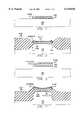
- FIGS. 1-2illustrate LOCOS with nitride mask 102 on pad oxide 104 which is on silicon wafer 106.
- FIG. 1is prior to thermal oxidation and FIG. 2 is after thermal oxidation which forms isolation oxide 108.
- the bird's beak 110 growthwarps nitride 102 and may also generate defects in the adjacent silicon wafer due to the stresses generated.
- FIGS. 3-4illustrate a form of PBL with nitride mask 302 on polysilicon buffer 303 which is on pad oxide 304.
- nitride mask 102 after LOCOS thermal oxidation or nitride mask 302 after PBL thermal oxidationrequires a nitride or a nitride plus polysilicon etch which will stop on the pad oxide and thereby avoid damaging the underlying device area silicon.
- the standard nitride etchuses a bath of hot phosphoric acid (H 3 PO 4 ) which is highly selective to oxide.
- wet etchesintroduce undesired contamination of a wafer for two reasons: liquids typically cannot be purified sufficiently and the wafer must be removed from the oxidation chamber for the wet nitride stripping (plus pad oxide removal and cleanup) and then reinserted into a processing chamber for subsequent steps, typically a thermal oxidation to form gate oxide.
- An all dry processing sequence for nitride strippingcan avoid the wet etch and the removal/reinsertion contamination sources.
- Nitride and polysiliconcan also be used in other integrated circuit processing steps which require isotropic stripping. For example, vias in an oxide insulating layer can be filled by blanket polysilicon deposition followed by an etchback. Similarly, a wafer with a nitride backside seal and a frontside deposited protective oxide may require a selective nitride strip to avoid disturbing the frontside oxide.
- the present inventionprovides dry isotropic etches for silicon nitride, (poly)silicon, and silicon oxynitrides based on oxygen and/or nitrogen control gasses added to fluorine plus chlorine etch gasses to adjust selectivites as needed.
- FIGS. 1-2illustrate LOCOS in cross sectional elevational views.
- FIGS. 3-4show polysilicon buffered LOCOS (PBL) in cross sectional elevational views.
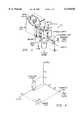
- FIG. 5is a perspective view of a remote plasma reactor.
- FIG. 6illustrates preferred embodiment etch chemistries.
- the preferred embodimentsinclude isotropic dry etches based on remote plasma generated speices of fluorine and chlorine (from sources such as NF 3 and Cl 2 ) with added nitrogen and/or oxygen to control selectivity and etch rates.
- Such etchescan strip silicon nitride ("nitride”) selectively with respect to polysilicon and silicon dioxide (“oxide”), strip polysilicon plus nitride selectively with respect to oxide, strip polysilicon selectively with respect to nitride and oxide, and strip silicon oxynitrides.
- nitridesilicon nitride
- oxidesilicon dioxide
- strip polysilicon plus nitrideselectively with respect to oxide
- strip silicon oxynitridesstrip silicon oxynitrides.
- FIG. 1shows in cross sectional elevation view a portion of silicon wafer 106 with a nitride mask 102 and pad oxide 104 prior to LOCOS thermal oxidation
- FIG. 3shows the corresponding view for polysilicon buffered LOCOS (PBL) with recessed isolation oxide.
- PBLpolysilicon buffered LOCOS
- FIG. 3shows mask nitride 302 on polysilicon buffer layer 303 on pad oxide 304 with silicon wafer 306 recessed away from this nitride-polysilicon-oxide stack.
- nitride thicknessestypically are on the order of 0.1-0.3 ⁇ m (1000-3000 ⁇ ), polysilicon (if used) on the order of 0.05-0.1 ⁇ m (500-1000 ⁇ ), and pad oxide on the order of 0.01 ⁇ m (100 ⁇ ).
- the unbuffered, unrecessed LOCOS of FIG. 1looks like FIG. 2 and the buffered, recessed PBL of FIG. 3 looks like FIG. 4.
- the exposed surface of nitride 102, 302is oxidized to silicon oxynitride (SiO x N y ) 112, 312.
- the composition of the oxynitridevaries; the oxygen fraction decreases in a direction from the surface to the interior.
- nitride 102 plus oxynitride 112must be removed without also removing oxide 104 and attacking silicon 106.
- first oxynitride 312, then nitride 302, and lastly polysilicon 303must be removed without disturbing underlying silicon 306.
- the preferred embodimentsemploy a dry etch in a single chamber with a remote plasma source to generate active etch species but without ion impact and radiation which occurs in plasma etches. Indeed, removal of the oxynitride 112 and 312 require an isotropic etch due to their roughly vertical sidewall portions, so the directionality of a plasma or reactive ion etch should be avoided. And selectivity is needed because nonuniformities demand an overetch to insure clearance.
- FIG. 5illustrates remote plasma reactor 500 which can use the preferred embodiment etch chemistries.
- reactor 500can handle wafers up to 8 inches in diameter and has a cylindrical process chamber of roughly 15 cm high by 20 cm diameter.
- An alternative to the hotplate heater shown in FIG. 5would be an array of lamps to form a rapid thermal heater.
- the quartz tube from the plasma (inside the microwave cavity) to the waferhas a length of about 25 cm and an inside diameter of about 2.5 cm.
- Stripping the oxidation mask of the LOCOS of FIG. 2starts with an oxynitride etch using NF 3 plus O 2 and then applies a nitride etch using NF 3 , Cl 2 , O 2 , and N 2 which is highly selective to oxide so pad oxide 104 can be preserved during overetch. Stripping the oxidation mask stack of the PBL of FIG.
- the first preferred embodiment nitride etchbegins with a wafer at a cool room temperature (15° C.) in the process chamber of a remote plasma reactor as illustrated in FIG. 5. Then set a gas flow of 50 sccm (standard cubic centimeters per second) NF 3 , 25 sccm Cl 2 , 1500 sccm O 2 , and 1000 sccm N 2 into the microwave cavity for excitation, and maintain a process chamber total pressure of 2.0 Torr.
- sccmstandard cubic centimeters per second
- This nitride etchis selective with respect to oxide in that the etch rate for nitride is 7.17 ⁇ /sec and the etch rate for oxide is 0.49 ⁇ /sec. Thus the etch rates have a ratio of about 15 to 1. And the etch is also somewhat selective with respect to polysilicon in that the etch rate for polysilicon is 2.62 ⁇ /sec, so the etch rates have a ratio of about 3 to 1.
- a second embodiment isotropic nitride etchincreases the nitrogen flow by ten percent and thereby increases the selectivity without greatly decreasing the etch rate.
- the selectivity with respect to oxideis about 22 to 1
- the selectivity with respect to polysiliconis greater than 4.5 to 1.
- the gas mixturecan be adjusted to increase the nitrogen, chlorine, and fluorine and decrease the oxygen to a gas flow of 200 sccm NF 3 , 275 sccm Cl 2 , 680 sccm O 2 , and 2200 sccm N 2 while maintaining a process chamber total pressure of 2.0 Torr.
- the gas mixtureis excited with 1300 watts of 2.45 GHz power, and the resulting species transported to the wafer which is at 15° C. This etches nitride at 16.8 ⁇ /sec and oxide at 0.4 ⁇ /sec.
- the etch rateshave a ratio of about 40 to 1. Note that the etch rate for with this gas for polysilicon is 150.6 ⁇ /sec, and thus may be used as a selective polysilicon etch.
- a drop in effluent silicon compoundscan be used as an endpoint detection to terminate the etch.
- the first preferred embodiment polysilicon plus nitride etchbegins with a wafer at a cool room temperature (15° C.) in the process chamber of a remote plasma reactor as illustrated in FIG. 5. Then set a gas flow of 200 sccm NF 3 , 275 sccm Cl 2 , 680 sccm O 2 , and 2200 sccm N 2 into the microwave cavity for excitation, and maintain a process chamber total pressure of 2.0 Torr.
- This etchis selective for polysilicon with respect to oxide in that the etch rate for polysilicon is 150.6 ⁇ /sec and the etch rate for oxide is 0.40 ⁇ /sec. Thus the etch rates have a ratio of about 375 to 1. And the etch is also selective for nitride with respect to oxide in that the etch rate for nitride is 16.8 ⁇ /sec, so the etch rates have a ratio of about 40 to 1. Also, the ratio of the polysilicon etch rate to the nitride etch rate is about 9 to 1, so the etch could be used as a polysilicon etch selective to both oxide and nitride.
- polysilicon etchwhich is selective for oxide derives from decreasing the gas flows as follows: set a gas flow of 100 sccm NF 3 , 30 sccm Cl 2 , 0 sccm O 2 , and 1100 sccm N 2 into the microwave cavity for excitation at 1200 watts, and again maintain a process chamber total pressure of 2.0 Torr and a wafer temperature of 15° C. This yields an etch rate for polysilicon of 80 ⁇ /sec and an etch rate for oxide of 0.2 ⁇ /sec. Thus the etch has a selectivity of about 400 to 1.
- a drop in effluent silicon compoundscan be used as an endpoint detection to terminate the etch.
- FIG. 2shows in cross sectional elevation view an enlarged portion of a LOCOS oxidation mask after thermal oxidation.
- oxynitride layer 112 thickness and compositionmay vary for a given thickness of isolation field oxide 108 because the thermal oxidation may be performed in various ways which give rise to differing oxynitride layers.
- higher temperature and higher pressure thermal oxidationgenerally gives a relatively oxygen richer and thicker oxynitride layer, although for sufficiently high temperatures and pressures the field oxide may be formed so quickly that oxygen does not have time to diffuse too deeply into the nitride.
- the first preferred embodiment etch of the oxynitride plus nitride and stopping on pad oxide 104proceeds in two steps in the same reactor 500.
- the oxynitride etchwhich necessarily must etch oxide due to the possibility of fairly high oxygen content in the oxynitride, uses a wafer temperature of 250° C. and a total process chamber pressure of 4.5 Torr and the following gas flows: NF 3 at 100 sccm plus O 2 at 4000 sccm.
- For reactor 500apply about 1200 watts of microwave power (at 2.45 GHz) to dissociate NF 3 to yield atomic fluorine plus radicals such as NF and NF 2 , and dissociate O 2 to yield atomic oxygen.
- This chemistryetches oxide at about 12.2 ⁇ /sec, nitride at about 16.7 ⁇ /sec, and oxynitride at comparable rates depending upon the composition.
- This chemistryalso etches polysilicon at about 10.3 ⁇ /sec, so the etch could remove oxynitride 112, all of nitride 102, pad oxide 104, plus some of silicon wafer 106 if not timely terminated. Because the exposed portions of field oxide 108 are also being removed, endpoint detection by a drop in oxide etch products cannot be used. However, knowledge of the thermal oxidation process parameters (time, temperature, pressure, and oxidizing ambient) gives an estimate of the thickness of oxynitride 112. For example, a thermal oxidation producing a 0.8 ⁇ m thick field oxide will generate oxynitride roughly from 200 to 400 ⁇ thick for conditions of 850° C. at atmospheric pressure to 975° C. at 25 atmospheres pressure.
- the oxynitridewill typically be much thinner than the underlying nitride 102, and the oxynitride etch can easily be stopped in nitride 102. Typically, 25-30 seconds of etch would clear 150-200 ⁇ of oxynitride with an overetch.
- oxynitride 112has been totally removed (overetch)
- drop the temperature of wafer 106to about a cool room temperature (15° C.) and switch to a gas flow of 200 sccm NF 3 , 275 sccm Cl 2 , 680 sccm O 2 , and 2200 sccm N 2 with a process chamber total pressure of 2.0 Torr.
- flow only nitrogenwhich acts as an inert carrier gas. Raise the microwave power level to 1300 watts for the nitride etch.
- This nitride etchis selective with respect to oxide in that the etch rate for nitride is 16.8 ⁇ /sec and the etch rate for oxide is 0.4 ⁇ /sec. Thus the etch has a ratio of more than 40 to 1. And once the nitride has cleared, a drop in effluent silicon compounds can be used as an endpoint detection to terminate the etch.
- This etchremoves 2000 ⁇ of nitride with a 10% overetch in about 130 seconds, and the 10% overetch should only remove about 5 ⁇ of underlying pad oxide 104.
- the mask nitrideis removed without exposure of the underlying silicon 106 by a dry process in a single chamber.
- FIG. 4shows in cross sectional elevation view an enlarged portion of a polysilicon buffered LOCOS oxidation mask after thermal oxidation. Note that the oxynitride layer 312 thickness and composition again may vary for a given thickness of isolation field oxide 308 because the thermal oxidation may be performed in various ways which give rise to differing oxynitride layers.
- the second preferred embodiment etch of the oxynitride, nitride, plus polysilicon and stopping on pad oxide 304proceeds in three steps in the same reactor 500.
- the oxynitride etchwhich necessarily must etch oxide due to the possibility of fairly high oxygen content oxynitride, uses a wafer temperature of 250° C. and a total process chamber pressure of 4.5 Torr and the following gas flows: NF 3 at 100 sccm (standard cubic centimeters per second) plus O 2 at 4000 sccm.
- reactor 500apply about 1200 watts of microwave power (2.45 GHz) to dissociate NF 3 to yield atomic fluorine plus radicals such as NF and NF 2 , and dissociate O 2 to yield atomic oxygen.
- This chemistryetches oxide at about 12.2 ⁇ /sec, nitride at about 16.7 ⁇ /sec, oxynitride at comparable rates depending upon the composition, and polysilicon at 10.3 ⁇ /sec.
- oxynitride 312the thickness of oxynitride 312.
- the oxynitridewill typically be much thinner than the underlying nitride 302, and the oxynitride etch can easily be stopped in nitride 302. Typically, 25-30 seconds of etch would clear 150-200 ⁇ of oxynitride with an overetch.
- oxynitride 312has been totally removed (overetch)
- flow only nitrogenwhich acts as an inert carrier gas.
- Set the microwave power levelat 1300 watts for the nitride etch.
- This nitride etchis selective with respect to oxide in that the etch rate for nitride is 7.2 ⁇ /sec and the etch rate for oxide is 0.5 ⁇ /sec; but the etch rate for polysilicon is 2.6 ⁇ /sec, so the selectivity with respect to polysilicon is only about 3 to 1.
- polysilicon buffer layer 303has a thickness 500 ⁇ and thus stops the nitride etch even with a 10% overetch of a 2500 ⁇ thick nitride 302. Indeed, a 10% overetch of 2500 ⁇ of nitride takes about 380 seconds and removes only about 100 ⁇ of polysilicon 303.
- the nitridecould be stripped with a slower but more selective etch as follows. Again, after the oxynitride strip, lower the temperature to 15° C. and process chamber pressure to 2.0 Torr and switch to a gas flow of 50 sccm NF 3 , 25 sccm Cl 2 , 1500 sccm O 2 , and 1100 sccm N 2 and 1200 watts of microwave power. This nitride etch removes nitride at 6.5 ⁇ /sec, oxide at 0.3 ⁇ /sec, and polysilicon at 1.4 ⁇ /sec, so the selectivity with respect to oxide is about 22 to 1 and with respect to polysilicon is about 4.5 to 1. Thus stopping in the polysilicon is easier than with the previous nitride etch.
- the gas flowAfter the nitride etch, switch the gas flow to 200 sccm NF 3 , 275 sccm Cl 2 , 680 sccm O 2 , and 2200 sccm N 2 with a process chamber total pressure remaining at 2.0 Torr for a polysilicon etch.
- This polysilicon etchis selective with respect to oxide (and nitride) in that the etch rate for polysilicon is 151 ⁇ /sec, whereas the etch rate for oxide is 0.4 ⁇ /sec (and the nitride etch rate is 16.8 ⁇ /sec).
- the etchhas a ratio of more than 300 to 1 with respect to oxide (and 9 to 1 respect to nitride).
- This etchremoves 500 ⁇ of polysilicon with a 100% overetch in about 7 seconds, which would only remove 3 ⁇ of pad oxide 304.
- the slower but more selective polysilicon etchcould be used as follows. Again after the nitride etch, switch the gas flow to 100 sccm NF 3 , 30 sccm Cl 2 , 0 sccm O 2 , and 1100 sccm N 2 with a process chamber total pressure again remaining at 2.0 Torr and wafer temperature at 15° C. Then etch rate for polysilicon is 80 ⁇ /sec, whereas the etch rate for oxide is 0.2 ⁇ /sec for a selectivity of about 400 to 1.
- FIG. 6illustrates the preferred embodiment etches as functions of the oxygen to fluorine ratio, the nitrogen to flourine ratio, and the chlorine to fluorine ratio. Perturbations in the etch compositions and conditions will yield etches which still provide most of the etch selectivities and rates as the preferred embodiments.
- the oxygen and nitrogen control gas flowsmay be adjusted to vary the etch rates and still maintain selectivities such as nitride to oxide of at least 10 to 1 together with nitride to polysilicon of at least 2 to 1, or polysilicon to oxide of at least 100 to 1 together with nitride to oxide of at least 20 to 1, or polysilicon to oxide of at least 100 to 1 together with polysilicon to nitride of at least 5 to 1.
- Various compoundsmay be substituted for the foregoing ingredients.
- other sources of atomic fluorinesuch as SF 6 , F 2 , CF 4 , and so forth may be used in place of or in addition to the NF 3 .
- fluorocarbonsshould be avoided in oxygen-deficient environments to prevent formation of polymers.
- other sources of chlorinesuch as HCl, NCl 3 , may be used, although such sources would generate atomic chlorine and thus not as rapid reaction with fluorine if the primary reaction were something like F+Cl 2 ⁇ ClF+Cl.
- ClF and ClF 3could be directly used.
- oxygen and nitrogencould include NO 2 , O 3 , and so forth; the oxygen provides an oxidizer and nitrogen provides a carrier gas.
- Inert carrier gassessuch as He, Ar, . . . could be used.
- bromine or iodine in place of chlorinewill also suffice because BrF and IF also would not dissociate on oxide.
- compoundssuch as BrF 3 , BrF 5 , IF 5 , . . . could be used directly, or Br 2 replacing Cl 2 , or even a mixture of both Cl and Br compounds.
- the preferred embodimentsmay be varied in many ways while retaining one or more of the features of a dry isotropic etch of nitride and/or (poly)silicon relative to oxide based on oxygen and/or nitrogen addition to a fluorine-chlorine etch for control of the etch selectivities.
- the pressure and temperature in the process chambercould be varied; the gas flow, the excitation power, the excitation frequency, and the degree of dissociation could be varied, indeed, multiple excitation power sources with differing frequencies and magnetic confinement fields could be used.
- the degree of reaction among the excited speciescould be adjusted by changing the length of the transport path from the excitation location to the process chamber.
Landscapes
- Engineering & Computer Science (AREA)
- Computer Hardware Design (AREA)
- Physics & Mathematics (AREA)
- Condensed Matter Physics & Semiconductors (AREA)
- General Physics & Mathematics (AREA)
- Manufacturing & Machinery (AREA)
- Chemical & Material Sciences (AREA)
- Microelectronics & Electronic Packaging (AREA)
- Power Engineering (AREA)
- General Chemical & Material Sciences (AREA)
- Inorganic Chemistry (AREA)
- Chemical Kinetics & Catalysis (AREA)
- Local Oxidation Of Silicon (AREA)
Abstract
Description
This invention was made with Government support. The Government has certain rights in this invention.
The following applications contain subject matter related to the present application and are assigned to the assignee of the present application: cofiled applications with Ser. Nos. 08/235,819 and 08/236,788, now U.S. Pat. No. 5,437,765.
The invention relates to electronic semiconductor devices, and, more particularly, to fabrication of silicon-based devices.
Silicon integrated circuits typically electrically isolate individual field effect transistors, bipolar transistors, and any substrate resistors and other elements with silicon dioxide ("oxide") regions at the surface of a silicon wafer. These oxide isolation regions can be directly formed by a thermal oxidation of a silicon wafer with an oxidation barrier such as silicon nitride ("nitride") masking off areas which will eventually contain transistors, substrate resistors, and other elements. This method of oxidation of selected regions of a silicon wafer has acquired the acronym LOCOS ("local oxidation of silicon"). See for example, Runyan and Bean, Semiconductor Integrated Circuit Processing Technology (Addison-Wesley 1990) pages 108-110.
Typical LOCOS includes using a thin oxide layer between the nitride mask and the silicon wafer; this oxide provides stress relief during the thermal oxidation. However, thermal oxidation of silicon proceeds essentially isotropically, and the oxidation encroaches under the nitride mask along the pad oxide to form an oxide wedge termed the "bird's beak". FIGS. 1-2 illustrate LOCOS withnitride mask 102 onpad oxide 104 which is onsilicon wafer 106. FIG. 1 is prior to thermal oxidation and FIG. 2 is after thermal oxidation which formsisolation oxide 108. The bird's beak 110growth warps nitride 102 and may also generate defects in the adjacent silicon wafer due to the stresses generated.
The bird's beak limits the scaling down and packing density of the devices in an integrated circuit. Thus attempts to reduce the extent of the bird's beak have been made and include making the pad oxide thinner and inserting a polycrystalline silicon ("polysilicon") layer between the nitride and the pad oxide ("poly buffered LOCOS" or "PBL"). FIGS. 3-4 illustrate a form of PBL withnitride mask 302 onpolysilicon buffer 303 which is onpad oxide 304.
Removal of thenitride mask 102 after LOCOS thermal oxidation ornitride mask 302 after PBL thermal oxidation requires a nitride or a nitride plus polysilicon etch which will stop on the pad oxide and thereby avoid damaging the underlying device area silicon. The standard nitride etch uses a bath of hot phosphoric acid (H3 PO4) which is highly selective to oxide. However, wet etches introduce undesired contamination of a wafer for two reasons: liquids typically cannot be purified sufficiently and the wafer must be removed from the oxidation chamber for the wet nitride stripping (plus pad oxide removal and cleanup) and then reinserted into a processing chamber for subsequent steps, typically a thermal oxidation to form gate oxide. An all dry processing sequence for nitride stripping can avoid the wet etch and the removal/reinsertion contamination sources.
Nitride and polysilicon can also be used in other integrated circuit processing steps which require isotropic stripping. For example, vias in an oxide insulating layer can be filled by blanket polysilicon deposition followed by an etchback. Similarly, a wafer with a nitride backside seal and a frontside deposited protective oxide may require a selective nitride strip to avoid disturbing the frontside oxide.
Suto et al, Highly Selective Etching of Si3 N4 to SiO2 Employing Fluorine and Chlorine Atoms Generated by Microwave Discharge, 136 JECS 2132 (1989), report the selective etching of nitride with respect to oxide with the interhalogen compound ClF. Suto et al generated the ClF by Cl2 reacting with F atoms derived from an NF3 plasma.
Loewenstein et al, Chemical Etching of Thermally Oxidized Silicon Nitride: Comparison of Wet and Dry Etching Methods, 138 JECS 1389 (1991), compare methods of stripping the LOCOS nitride. Note that the nitride becomes oxidized at its surface to form a silicon oxynitride during the LOCOS thermal oxidation, and thus etch selectivity with respect to oxide may slow down the nitride etch but is necessary to stop on the underlying pad oxide. Thus there is a problem of efficiently stripping nitride selectively over oxide and polysilicon and of efficiently stripping polysilicon selectively over oxide and nitride.
The present invention provides dry isotropic etches for silicon nitride, (poly)silicon, and silicon oxynitrides based on oxygen and/or nitrogen control gasses added to fluorine plus chlorine etch gasses to adjust selectivites as needed.
This has advantages including the totally dry stripping of the oxdiation masks in local oxidation of silicon by sequential use of these etches.
The drawings are schematic for clarity.
FIGS. 1-2 illustrate LOCOS in cross sectional elevational views.
FIGS. 3-4 show polysilicon buffered LOCOS (PBL) in cross sectional elevational views.
FIG. 5 is a perspective view of a remote plasma reactor.
FIG. 6 illustrates preferred embodiment etch chemistries.
The preferred embodiments include isotropic dry etches based on remote plasma generated speices of fluorine and chlorine (from sources such as NF3 and Cl2) with added nitrogen and/or oxygen to control selectivity and etch rates. Such etches can strip silicon nitride ("nitride") selectively with respect to polysilicon and silicon dioxide ("oxide"), strip polysilicon plus nitride selectively with respect to oxide, strip polysilicon selectively with respect to nitride and oxide, and strip silicon oxynitrides. This permits removal of the various oxidation masking materials used in local oxidation of silicon; namely, silicon nitride, silicon oxynitrides, and polysilicon. The various materials may be stripped sequentially without removal of a wafer from the etcher; this lessens particulate contamination.
FIG. 1 shows in cross sectional elevation view a portion ofsilicon wafer 106 with anitride mask 102 andpad oxide 104 prior to LOCOS thermal oxidation, and FIG. 3 shows the corresponding view for polysilicon buffered LOCOS (PBL) with recessed isolation oxide. In particular, FIG. 3 showsmask nitride 302 onpolysilicon buffer layer 303 onpad oxide 304 withsilicon wafer 306 recessed away from this nitride-polysilicon-oxide stack. Note that nitride thicknesses typically are on the order of 0.1-0.3 μm (1000-3000 Å), polysilicon (if used) on the order of 0.05-0.1 μm (500-1000 Å), and pad oxide on the order of 0.01 μm (100 Å). After thermal oxidation, the unbuffered, unrecessed LOCOS of FIG. 1 looks like FIG. 2 and the buffered, recessed PBL of FIG. 3 looks like FIG. 4. Note that in both cases the exposed surface ofnitride
For the LOCOS of FIG. 2,nitride 102 plusoxynitride 112 must be removed without also removingoxide 104 and attackingsilicon 106. Similarly, for the PBL of FIG. 4,first oxynitride 312, thennitride 302, and lastlypolysilicon 303 must be removed without disturbingunderlying silicon 306. The preferred embodiments employ a dry etch in a single chamber with a remote plasma source to generate active etch species but without ion impact and radiation which occurs in plasma etches. Indeed, removal of theoxynitride
FIG. 5 illustratesremote plasma reactor 500 which can use the preferred embodiment etch chemistries. Note thatreactor 500 can handle wafers up to 8 inches in diameter and has a cylindrical process chamber of roughly 15 cm high by 20 cm diameter. An alternative to the hotplate heater shown in FIG. 5 would be an array of lamps to form a rapid thermal heater. The quartz tube from the plasma (inside the microwave cavity) to the wafer has a length of about 25 cm and an inside diameter of about 2.5 cm.
Stripping the oxidation mask of the LOCOS of FIG. 2 starts with an oxynitride etch using NF3 plus O2 and then applies a nitride etch using NF3, Cl2, O2, and N2 which is highly selective to oxide sopad oxide 104 can be preserved during overetch. Stripping the oxidation mask stack of the PBL of FIG. 4 also starts with the oxynitride etch of NF3 plus O2, next applies a nitride etch using NF3, Cl2, O2, and N2 which is somewhat selective to polysilicon, and lastly applies a polysilicon etch with the same gasses as the nitride etch but in different ratios to be selective to nitride and highly selective to oxide. The switching from one etch to the next amounts to adjusting the flow of gasses intoreactor 500, and either end point detection or just timing determines the flow adjustments. Details of these etches appear in the following sections.
The first preferred embodiment nitride etch begins with a wafer at a cool room temperature (15° C.) in the process chamber of a remote plasma reactor as illustrated in FIG. 5. Then set a gas flow of 50 sccm (standard cubic centimeters per second) NF3, 25 sccm Cl2, 1500 sccm O2, and 1000 sccm N2 into the microwave cavity for excitation, and maintain a process chamber total pressure of 2.0 Torr. Set the microwave power level to 1300 watts at 2.45 GHz; this dissociates some of the NF3 to yield atomic fluorine plus radicals such as NF and NF2, and dissociates some of the Cl2, N2, and O2 to yield atomic chlorine, atomic nitrogen, and atomic oxygen. Then transport these species to the wafer for isotropic etching.
This nitride etch is selective with respect to oxide in that the etch rate for nitride is 7.17 Å/sec and the etch rate for oxide is 0.49 Å/sec. Thus the etch rates have a ratio of about 15 to 1. And the etch is also somewhat selective with respect to polysilicon in that the etch rate for polysilicon is 2.62 Å/sec, so the etch rates have a ratio of about 3 to 1.
A second embodiment isotropic nitride etch increases the nitrogen flow by ten percent and thereby increases the selectivity without greatly decreasing the etch rate. In particular, set a gas flow of 50 sccm NF3, 25 sccm Cl2, 1500 sccm O2, and 1100 sccm N2 into the microwave cavity with 1200 watts excitation, and again maintain a process chamber total pressure of 2.0 Torr and a wafer temperature of 15° C. This changes the etch rate for nitride to 6.5 Å/sec, the etch rate for oxide to 0.3 Å/sec, and the etch rate for polysilicon to 1.4 Å/sec. Thus the selectivity with respect to oxide is about 22 to 1, and the selectivity with respect to polysilicon is greater than 4.5 to 1.
However, if there is no polysilicon exposed, and only the selectivity with respect to oxide is needed, then the gas mixture can be adjusted to increase the nitrogen, chlorine, and fluorine and decrease the oxygen to a gas flow of 200 sccm NF3, 275 sccm Cl2, 680 sccm O2, and 2200 sccm N2 while maintaining a process chamber total pressure of 2.0 Torr. Again, the gas mixture is excited with 1300 watts of 2.45 GHz power, and the resulting species transported to the wafer which is at 15° C. This etches nitride at 16.8 Å/sec and oxide at 0.4 Å/sec. Thus the etch rates have a ratio of about 40 to 1. Note that the etch rate for with this gas for polysilicon is 150.6 Å/sec, and thus may be used as a selective polysilicon etch.
Once the nitride has cleared, a drop in effluent silicon compounds can be used as an endpoint detection to terminate the etch.
The first preferred embodiment polysilicon plus nitride etch begins with a wafer at a cool room temperature (15° C.) in the process chamber of a remote plasma reactor as illustrated in FIG. 5. Then set a gas flow of 200 sccm NF3, 275 sccm Cl2, 680 sccm O2, and 2200 sccm N2 into the microwave cavity for excitation, and maintain a process chamber total pressure of 2.0 Torr. Set the microwave power level to 1300 watts at 2.45 GHz; this dissociates some of the NF3 to yield atomic fluorine plus radicals such as NF and NF2, and dissociates some of the Cl2, N2, and O2 to yield atomic chlorine, atomic nitrogen, and atomic oxygen. Then transport these species to the wafer for isotropic etching.
This etch is selective for polysilicon with respect to oxide in that the etch rate for polysilicon is 150.6 Å/sec and the etch rate for oxide is 0.40 Å/sec. Thus the etch rates have a ratio of about 375 to 1. And the etch is also selective for nitride with respect to oxide in that the etch rate for nitride is 16.8 Å/sec, so the etch rates have a ratio of about 40 to 1. Also, the ratio of the polysilicon etch rate to the nitride etch rate is about 9 to 1, so the etch could be used as a polysilicon etch selective to both oxide and nitride.
Another embodiment polysilicon etch which is selective for oxide derives from decreasing the gas flows as follows: set a gas flow of 100 sccm NF3, 30 sccm Cl2, 0 sccm O2, and 1100 sccm N2 into the microwave cavity for excitation at 1200 watts, and again maintain a process chamber total pressure of 2.0 Torr and a wafer temperature of 15° C. This yields an etch rate for polysilicon of 80 Å/sec and an etch rate for oxide of 0.2 Å/sec. Thus the etch has a selectivity of about 400 to 1.
Once the polysilicon has cleared, a drop in effluent silicon compounds can be used as an endpoint detection to terminate the etch.
FIG. 2 shows in cross sectional elevation view an enlarged portion of a LOCOS oxidation mask after thermal oxidation. Note thatoxynitride layer 112 thickness and composition may vary for a given thickness ofisolation field oxide 108 because the thermal oxidation may be performed in various ways which give rise to differing oxynitride layers. In particular, higher temperature and higher pressure thermal oxidation generally gives a relatively oxygen richer and thicker oxynitride layer, although for sufficiently high temperatures and pressures the field oxide may be formed so quickly that oxygen does not have time to diffuse too deeply into the nitride.
The first preferred embodiment etch of the oxynitride plus nitride and stopping onpad oxide 104 proceeds in two steps in thesame reactor 500. The oxynitride etch, which necessarily must etch oxide due to the possibility of fairly high oxygen content in the oxynitride, uses a wafer temperature of 250° C. and a total process chamber pressure of 4.5 Torr and the following gas flows: NF3 at 100 sccm plus O2 at 4000 sccm. Forreactor 500 apply about 1200 watts of microwave power (at 2.45 GHz) to dissociate NF3 to yield atomic fluorine plus radicals such as NF and NF2, and dissociate O2 to yield atomic oxygen. Then transport these species towafer 106 for thermal etching. This chemistry etches oxide at about 12.2 Å/sec, nitride at about 16.7 Å/sec, and oxynitride at comparable rates depending upon the composition.
This chemistry also etches polysilicon at about 10.3 Å/sec, so the etch could removeoxynitride 112, all ofnitride 102,pad oxide 104, plus some ofsilicon wafer 106 if not timely terminated. Because the exposed portions offield oxide 108 are also being removed, endpoint detection by a drop in oxide etch products cannot be used. However, knowledge of the thermal oxidation process parameters (time, temperature, pressure, and oxidizing ambient) gives an estimate of the thickness ofoxynitride 112. For example, a thermal oxidation producing a 0.8 μm thick field oxide will generate oxynitride roughly from 200 to 400 Å thick for conditions of 850° C. at atmospheric pressure to 975° C. at 25 atmospheres pressure. See the Loewenstein article cited in the Background. Thus the oxynitride will typically be much thinner than theunderlying nitride 102, and the oxynitride etch can easily be stopped innitride 102. Typically, 25-30 seconds of etch would clear 150-200 Å of oxynitride with an overetch.
Onceoxynitride 112 has been totally removed (overetch), drop the temperature ofwafer 106 to about a cool room temperature (15° C.) and switch to a gas flow of 200 sccm NF3, 275 sccm Cl2, 680 sccm O2, and 2200 sccm N2 with a process chamber total pressure of 2.0 Torr. During the cooling down from the oxynitride etch temperature to the nitride etch temperature, flow only nitrogen, which acts as an inert carrier gas. Raise the microwave power level to 1300 watts for the nitride etch. This nitride etch is selective with respect to oxide in that the etch rate for nitride is 16.8 Å/sec and the etch rate for oxide is 0.4 Å/sec. Thus the etch has a ratio of more than 40 to 1. And once the nitride has cleared, a drop in effluent silicon compounds can be used as an endpoint detection to terminate the etch.
This etch removes 2000 Å of nitride with a 10% overetch in about 130 seconds, and the 10% overetch should only remove about 5 Å ofunderlying pad oxide 104. Thus the mask nitride is removed without exposure of theunderlying silicon 106 by a dry process in a single chamber.
FIG. 4 shows in cross sectional elevation view an enlarged portion of a polysilicon buffered LOCOS oxidation mask after thermal oxidation. Note that theoxynitride layer 312 thickness and composition again may vary for a given thickness ofisolation field oxide 308 because the thermal oxidation may be performed in various ways which give rise to differing oxynitride layers.
The second preferred embodiment etch of the oxynitride, nitride, plus polysilicon and stopping onpad oxide 304 proceeds in three steps in thesame reactor 500. The oxynitride etch, which necessarily must etch oxide due to the possibility of fairly high oxygen content oxynitride, uses a wafer temperature of 250° C. and a total process chamber pressure of 4.5 Torr and the following gas flows: NF3 at 100 sccm (standard cubic centimeters per second) plus O2 at 4000 sccm. Forreactor 500 apply about 1200 watts of microwave power (2.45 GHz) to dissociate NF3 to yield atomic fluorine plus radicals such as NF and NF2, and dissociate O2 to yield atomic oxygen. This chemistry etches oxide at about 12.2 Å/sec, nitride at about 16.7 Å/sec, oxynitride at comparable rates depending upon the composition, and polysilicon at 10.3 Å/sec.
Again, knowledge of the thermal oxidation process parameters gives an estimate of the thickness ofoxynitride 312. The oxynitride will typically be much thinner than theunderlying nitride 302, and the oxynitride etch can easily be stopped innitride 302. Typically, 25-30 seconds of etch would clear 150-200 Å of oxynitride with an overetch.
Onceoxynitride 312 has been totally removed (overetch), drop the temperature ofwafer 306 to about 15° C. and switch to a gas flow of 50 sccm NF3, 25 sccm Cl2, 1500 sccm O2, and 1000 sccm N2 with a process chamber total pressure of 2.0 Torr. During the cooling down from the oxynitride etch temperature to the nitride etch temperature, flow only nitrogen, which acts as an inert carrier gas. Set the microwave power level at 1300 watts for the nitride etch. This nitride etch is selective with respect to oxide in that the etch rate for nitride is 7.2 Å/sec and the etch rate for oxide is 0.5 Å/sec; but the etch rate for polysilicon is 2.6 Å/sec, so the selectivity with respect to polysilicon is only about 3 to 1. However,polysilicon buffer layer 303 has athickness 500 Å and thus stops the nitride etch even with a 10% overetch of a 2500 Åthick nitride 302. Indeed, a 10% overetch of 2500 Å of nitride takes about 380 seconds and removes only about 100 Å ofpolysilicon 303.
Alternatively, the nitride could be stripped with a slower but more selective etch as follows. Again, after the oxynitride strip, lower the temperature to 15° C. and process chamber pressure to 2.0 Torr and switch to a gas flow of 50 sccm NF3, 25 sccm Cl2, 1500 sccm O2, and 1100 sccm N2 and 1200 watts of microwave power. This nitride etch removes nitride at 6.5 Å/sec, oxide at 0.3 Å/sec, and polysilicon at 1.4 Å/sec, so the selectivity with respect to oxide is about 22 to 1 and with respect to polysilicon is about 4.5 to 1. Thus stopping in the polysilicon is easier than with the previous nitride etch.
After the nitride etch, switch the gas flow to 200 sccm NF3, 275 sccm Cl2, 680 sccm O2, and 2200 sccm N2 with a process chamber total pressure remaining at 2.0 Torr for a polysilicon etch. This polysilicon etch is selective with respect to oxide (and nitride) in that the etch rate for polysilicon is 151 Å/sec, whereas the etch rate for oxide is 0.4 Å/sec (and the nitride etch rate is 16.8 Å/sec). Thus the etch has a ratio of more than 300 to 1 with respect to oxide (and 9 to 1 respect to nitride). And once thepolysilicon 303 has cleared, a drop in effluent silicon compounds can be used as an endpoint detection to terminate the etch. Note that this same etch was used to stripnitride 102 in the oxynitride-nitride-oxide stack embodiment due to the very low oxide etching rate.
This etch removes 500 Å of polysilicon with a 100% overetch in about 7 seconds, which would only remove 3 Å ofpad oxide 304.
Alternatively, the slower but more selective polysilicon etch could be used as follows. Again after the nitride etch, switch the gas flow to 100 sccm NF3, 30 sccm Cl2, 0 sccm O2, and 1100 sccm N2 with a process chamber total pressure again remaining at 2.0 Torr and wafer temperature at 15° C. Then etch rate for polysilicon is 80 Å/sec, whereas the etch rate for oxide is 0.2 Å/sec for a selectivity of about 400 to 1.
FIG. 6 illustrates the preferred embodiment etches as functions of the oxygen to fluorine ratio, the nitrogen to flourine ratio, and the chlorine to fluorine ratio. Perturbations in the etch compositions and conditions will yield etches which still provide most of the etch selectivities and rates as the preferred embodiments. In particular, the oxygen and nitrogen control gas flows may be adjusted to vary the etch rates and still maintain selectivities such as nitride to oxide of at least 10 to 1 together with nitride to polysilicon of at least 2 to 1, or polysilicon to oxide of at least 100 to 1 together with nitride to oxide of at least 20 to 1, or polysilicon to oxide of at least 100 to 1 together with polysilicon to nitride of at least 5 to 1.
Various compounds may be substituted for the foregoing ingredients. In particular, other sources of atomic fluorine, such as SF6, F2, CF4, and so forth may be used in place of or in addition to the NF3. However, fluorocarbons should be avoided in oxygen-deficient environments to prevent formation of polymers. Similarly, other sources of chlorine such as HCl, NCl3, may be used, although such sources would generate atomic chlorine and thus not as rapid reaction with fluorine if the primary reaction were something like F+Cl2 →ClF+Cl. Of course, compounds such as ClF and ClF3 could be directly used. Other sources of oxygen and nitrogen could include NO2, O3, and so forth; the oxygen provides an oxidizer and nitrogen provides a carrier gas. Inert carrier gasses such as He, Ar, . . . could be used. Further, bromine or iodine in place of chlorine will also suffice because BrF and IF also would not dissociate on oxide. With other halogens substituted for chlorine, compounds such as BrF3, BrF5, IF5, . . . could be used directly, or Br2 replacing Cl2, or even a mixture of both Cl and Br compounds.
The preferred embodiments may be varied in many ways while retaining one or more of the features of a dry isotropic etch of nitride and/or (poly)silicon relative to oxide based on oxygen and/or nitrogen addition to a fluorine-chlorine etch for control of the etch selectivities.
For example, the pressure and temperature in the process chamber could be varied; the gas flow, the excitation power, the excitation frequency, and the degree of dissociation could be varied, indeed, multiple excitation power sources with differing frequencies and magnetic confinement fields could be used. The degree of reaction among the excited species could be adjusted by changing the length of the transport path from the excitation location to the process chamber.
Claims (13)
1. A method of dry etching polysilicon plus silicon nitride, comprising the steps of:
(a) exposing polysilicon plus silicon nitride to a gas mixture including fluorine and chlorine sources plus a control gas selected from the group consisting of an oxygen source, a nitrogen source, and a mixture thereof, whereby said polysilicon plus silicon nitride is removed.
2. The method of claim 1, wherein:
(a) said gas mixture of step (a) of claim 1 is excited in a plasma remote from said polysilicon and silicon nitride.
3. The method of claim 1, wherein:
(a) said gas mixture of step (a) of claim 1 contains more oxygen than flourine.
4. The method of claim 1, wherein:
(a) said gas mixture of step (a) of claim 1 contains more nitrogen than fluorine.
5. The method of claim 1, wherein:
(a) the ratios of nitrogen to fluorine and oxygen to fluorine are both greater than the ratio of chlorine to fluorine in said gas mixture.
6. The method of claim 1 with said polysilicon and silicon nitride adjacent silicon oxide, wherein:
(a) said gas mixture removes polysilicon at a rate of at least 100 times the rate it removes silicon oxide; and
(b) said gas mixture removes silicon nitride at a rate of at least 20 times the rate it removes silicon oxide.
7. The method of claim 6, wherein:
(a) said gas mixture is excited in a remote plasma; and
(b) said gas mixture included NF3 as a fluorine source, Cl2 as a chlorine source, N2 as a nitrogen source, and O2 as an oxygen source.
8. The method of claim 7, wherein:
(a) the ratio of N2 to NF3 and the ratio of O2 to NF3 are both at least 2 times the ratio of Cl2 to NF3.
9. A dry etch mixture for etching polysilicon, comprising:
(a) activated species from a remote excitation of a mixture of a fluorine source, a chlorine source, a nitrogen source, and an oxygen source, wherein said nitrogen source plus said oxygen source is at least about 85% of said mixture.
10. The etch mixture of claim 9, wherein:
(a) said flourine source includes NF3, said chlorine source includes Cl2, said nitrogen source includes N2, and said oxygen source includes O2.
11. The etch mixture of claim 10, wherein:
(a) the ratio of N2 to NF3 and the ratio of O2 to NF3 are both at least 2 times the ratio of Cl2 to NF3.
12. The etch mixture of claim 9 with said polysilicon adjacent silicon nitride and silicon oxide, wherein:
(a) said activated species remove polysilicon at a rate of at least 100 times the rate they remove silicon oxide; and
(b) said activated species remove polysilicon at a rate of at least 5 times the rate they remove silicon nitride.
13. A method of etching polysilicon, comprising the steps of:
(a) exposing polysilicon to a gas mixture including fluorine and chlorine sources plus a control gas which includes a nitrogen source, and an oxygen source, wherein said control gas is at least about 85% of said gas mixture.
Priority Applications (1)
| Application Number | Priority Date | Filing Date | Title |
|---|---|---|---|
| US08/235,726US6110838A (en) | 1994-04-29 | 1994-04-29 | Isotropic polysilicon plus nitride stripping |
Applications Claiming Priority (1)
| Application Number | Priority Date | Filing Date | Title |
|---|---|---|---|
| US08/235,726US6110838A (en) | 1994-04-29 | 1994-04-29 | Isotropic polysilicon plus nitride stripping |
Publications (1)
| Publication Number | Publication Date |
|---|---|
| US6110838Atrue US6110838A (en) | 2000-08-29 |
Family
ID=22886679
Family Applications (1)
| Application Number | Title | Priority Date | Filing Date |
|---|---|---|---|
| US08/235,726Expired - LifetimeUS6110838A (en) | 1994-04-29 | 1994-04-29 | Isotropic polysilicon plus nitride stripping |
Country Status (1)
| Country | Link |
|---|---|
| US (1) | US6110838A (en) |
Cited By (159)
| Publication number | Priority date | Publication date | Assignee | Title |
|---|---|---|---|---|
| US20070004127A1 (en)* | 2005-06-30 | 2007-01-04 | Jin Yul Lee | Method of fabricating a transistor having the round corner recess channel structure |
| US20090170263A1 (en)* | 2007-12-26 | 2009-07-02 | Ki-Min Lee | Method of manufacturing flash memory device |
| US20110079241A1 (en)* | 2009-10-01 | 2011-04-07 | Ashwini Sinha | Method for ion source component cleaning |
| US20110221748A1 (en)* | 2008-08-04 | 2011-09-15 | Sony Computer Entertainment Europe Limited | Apparatus and method of viewing electronic documents |
| US20130045605A1 (en)* | 2011-08-18 | 2013-02-21 | Applied Materials, Inc. | Dry-etch for silicon-and-nitrogen-containing films |
| US8664127B2 (en) | 2010-10-15 | 2014-03-04 | Applied Materials, Inc. | Two silicon-containing precursors for gapfill enhancing dielectric liner |
| US8716154B2 (en) | 2011-03-04 | 2014-05-06 | Applied Materials, Inc. | Reduced pattern loading using silicon oxide multi-layers |
| US20140199852A1 (en)* | 2011-08-25 | 2014-07-17 | Masahiro Kimura | Pattern forming method |
| US8801952B1 (en) | 2013-03-07 | 2014-08-12 | Applied Materials, Inc. | Conformal oxide dry etch |
| US8808563B2 (en) | 2011-10-07 | 2014-08-19 | Applied Materials, Inc. | Selective etch of silicon by way of metastable hydrogen termination |
| US8889566B2 (en) | 2012-09-11 | 2014-11-18 | Applied Materials, Inc. | Low cost flowable dielectric films |
| US8895449B1 (en) | 2013-05-16 | 2014-11-25 | Applied Materials, Inc. | Delicate dry clean |
| US8921234B2 (en) | 2012-12-21 | 2014-12-30 | Applied Materials, Inc. | Selective titanium nitride etching |
| US8927390B2 (en) | 2011-09-26 | 2015-01-06 | Applied Materials, Inc. | Intrench profile |
| US8951429B1 (en) | 2013-10-29 | 2015-02-10 | Applied Materials, Inc. | Tungsten oxide processing |
| US8956980B1 (en) | 2013-09-16 | 2015-02-17 | Applied Materials, Inc. | Selective etch of silicon nitride |
| US8969212B2 (en) | 2012-11-20 | 2015-03-03 | Applied Materials, Inc. | Dry-etch selectivity |
| US8999856B2 (en) | 2011-03-14 | 2015-04-07 | Applied Materials, Inc. | Methods for etch of sin films |
| US9018108B2 (en) | 2013-01-25 | 2015-04-28 | Applied Materials, Inc. | Low shrinkage dielectric films |
| US9023732B2 (en) | 2013-03-15 | 2015-05-05 | Applied Materials, Inc. | Processing systems and methods for halide scavenging |
| US9023734B2 (en) | 2012-09-18 | 2015-05-05 | Applied Materials, Inc. | Radical-component oxide etch |
| US9034770B2 (en) | 2012-09-17 | 2015-05-19 | Applied Materials, Inc. | Differential silicon oxide etch |
| US9040422B2 (en) | 2013-03-05 | 2015-05-26 | Applied Materials, Inc. | Selective titanium nitride removal |
| US9064815B2 (en) | 2011-03-14 | 2015-06-23 | Applied Materials, Inc. | Methods for etch of metal and metal-oxide films |
| US9064816B2 (en) | 2012-11-30 | 2015-06-23 | Applied Materials, Inc. | Dry-etch for selective oxidation removal |
| US9117855B2 (en) | 2013-12-04 | 2015-08-25 | Applied Materials, Inc. | Polarity control for remote plasma |
| US9114438B2 (en) | 2013-05-21 | 2015-08-25 | Applied Materials, Inc. | Copper residue chamber clean |
| US9136273B1 (en) | 2014-03-21 | 2015-09-15 | Applied Materials, Inc. | Flash gate air gap |
| US9132436B2 (en) | 2012-09-21 | 2015-09-15 | Applied Materials, Inc. | Chemical control features in wafer process equipment |
| US9144147B2 (en) | 2011-01-18 | 2015-09-22 | Applied Materials, Inc. | Semiconductor processing system and methods using capacitively coupled plasma |
| US9159606B1 (en) | 2014-07-31 | 2015-10-13 | Applied Materials, Inc. | Metal air gap |
| US9165786B1 (en) | 2014-08-05 | 2015-10-20 | Applied Materials, Inc. | Integrated oxide and nitride recess for better channel contact in 3D architectures |
| US9190293B2 (en) | 2013-12-18 | 2015-11-17 | Applied Materials, Inc. | Even tungsten etch for high aspect ratio trenches |
| US9236265B2 (en) | 2013-11-04 | 2016-01-12 | Applied Materials, Inc. | Silicon germanium processing |
| US9236266B2 (en) | 2011-08-01 | 2016-01-12 | Applied Materials, Inc. | Dry-etch for silicon-and-carbon-containing films |
| US9245762B2 (en) | 2013-12-02 | 2016-01-26 | Applied Materials, Inc. | Procedure for etch rate consistency |
| US9263278B2 (en) | 2013-12-17 | 2016-02-16 | Applied Materials, Inc. | Dopant etch selectivity control |
| US9269590B2 (en) | 2014-04-07 | 2016-02-23 | Applied Materials, Inc. | Spacer formation |
| US9285168B2 (en) | 2010-10-05 | 2016-03-15 | Applied Materials, Inc. | Module for ozone cure and post-cure moisture treatment |
| US9287134B2 (en) | 2014-01-17 | 2016-03-15 | Applied Materials, Inc. | Titanium oxide etch |
| US9287095B2 (en) | 2013-12-17 | 2016-03-15 | Applied Materials, Inc. | Semiconductor system assemblies and methods of operation |
| US9293568B2 (en) | 2014-01-27 | 2016-03-22 | Applied Materials, Inc. | Method of fin patterning |
| US9299537B2 (en) | 2014-03-20 | 2016-03-29 | Applied Materials, Inc. | Radial waveguide systems and methods for post-match control of microwaves |
| US9299538B2 (en) | 2014-03-20 | 2016-03-29 | Applied Materials, Inc. | Radial waveguide systems and methods for post-match control of microwaves |
| US9299575B2 (en) | 2014-03-17 | 2016-03-29 | Applied Materials, Inc. | Gas-phase tungsten etch |
| US9299583B1 (en) | 2014-12-05 | 2016-03-29 | Applied Materials, Inc. | Aluminum oxide selective etch |
| US9299582B2 (en) | 2013-11-12 | 2016-03-29 | Applied Materials, Inc. | Selective etch for metal-containing materials |
| US9309598B2 (en) | 2014-05-28 | 2016-04-12 | Applied Materials, Inc. | Oxide and metal removal |
| US9324576B2 (en) | 2010-05-27 | 2016-04-26 | Applied Materials, Inc. | Selective etch for silicon films |
| US9343272B1 (en) | 2015-01-08 | 2016-05-17 | Applied Materials, Inc. | Self-aligned process |
| US9349605B1 (en) | 2015-08-07 | 2016-05-24 | Applied Materials, Inc. | Oxide etch selectivity systems and methods |
| US9355856B2 (en) | 2014-09-12 | 2016-05-31 | Applied Materials, Inc. | V trench dry etch |
| US9355862B2 (en) | 2014-09-24 | 2016-05-31 | Applied Materials, Inc. | Fluorine-based hardmask removal |
| US9355863B2 (en) | 2012-12-18 | 2016-05-31 | Applied Materials, Inc. | Non-local plasma oxide etch |
| US9362130B2 (en) | 2013-03-01 | 2016-06-07 | Applied Materials, Inc. | Enhanced etching processes using remote plasma sources |
| US9368364B2 (en) | 2014-09-24 | 2016-06-14 | Applied Materials, Inc. | Silicon etch process with tunable selectivity to SiO2 and other materials |
| US9373522B1 (en) | 2015-01-22 | 2016-06-21 | Applied Mateials, Inc. | Titanium nitride removal |
| US9378969B2 (en) | 2014-06-19 | 2016-06-28 | Applied Materials, Inc. | Low temperature gas-phase carbon removal |
| US9378978B2 (en) | 2014-07-31 | 2016-06-28 | Applied Materials, Inc. | Integrated oxide recess and floating gate fin trimming |
| US9385028B2 (en) | 2014-02-03 | 2016-07-05 | Applied Materials, Inc. | Air gap process |
| US9390937B2 (en) | 2012-09-20 | 2016-07-12 | Applied Materials, Inc. | Silicon-carbon-nitride selective etch |
| US9396989B2 (en) | 2014-01-27 | 2016-07-19 | Applied Materials, Inc. | Air gaps between copper lines |
| US9406523B2 (en) | 2014-06-19 | 2016-08-02 | Applied Materials, Inc. | Highly selective doped oxide removal method |
| US9404178B2 (en) | 2011-07-15 | 2016-08-02 | Applied Materials, Inc. | Surface treatment and deposition for reduced outgassing |
| US9412608B2 (en) | 2012-11-30 | 2016-08-09 | Applied Materials, Inc. | Dry-etch for selective tungsten removal |
| US9412581B2 (en) | 2014-07-16 | 2016-08-09 | Applied Materials, Inc. | Low-K dielectric gapfill by flowable deposition |
| US9425058B2 (en) | 2014-07-24 | 2016-08-23 | Applied Materials, Inc. | Simplified litho-etch-litho-etch process |
| US9449846B2 (en) | 2015-01-28 | 2016-09-20 | Applied Materials, Inc. | Vertical gate separation |
| US9478432B2 (en) | 2014-09-25 | 2016-10-25 | Applied Materials, Inc. | Silicon oxide selective removal |
| US9493879B2 (en) | 2013-07-12 | 2016-11-15 | Applied Materials, Inc. | Selective sputtering for pattern transfer |
| US9496167B2 (en) | 2014-07-31 | 2016-11-15 | Applied Materials, Inc. | Integrated bit-line airgap formation and gate stack post clean |
| US9502258B2 (en) | 2014-12-23 | 2016-11-22 | Applied Materials, Inc. | Anisotropic gap etch |
| US9499898B2 (en) | 2014-03-03 | 2016-11-22 | Applied Materials, Inc. | Layered thin film heater and method of fabrication |
| US9553102B2 (en) | 2014-08-19 | 2017-01-24 | Applied Materials, Inc. | Tungsten separation |
| US9576809B2 (en) | 2013-11-04 | 2017-02-21 | Applied Materials, Inc. | Etch suppression with germanium |
| US9659753B2 (en) | 2014-08-07 | 2017-05-23 | Applied Materials, Inc. | Grooved insulator to reduce leakage current |
| US9691645B2 (en) | 2015-08-06 | 2017-06-27 | Applied Materials, Inc. | Bolted wafer chuck thermal management systems and methods for wafer processing systems |
| US9721789B1 (en) | 2016-10-04 | 2017-08-01 | Applied Materials, Inc. | Saving ion-damaged spacers |
| US9728437B2 (en) | 2015-02-03 | 2017-08-08 | Applied Materials, Inc. | High temperature chuck for plasma processing systems |
| US9741593B2 (en) | 2015-08-06 | 2017-08-22 | Applied Materials, Inc. | Thermal management systems and methods for wafer processing systems |
| US9768034B1 (en) | 2016-11-11 | 2017-09-19 | Applied Materials, Inc. | Removal methods for high aspect ratio structures |
| US9773648B2 (en) | 2013-08-30 | 2017-09-26 | Applied Materials, Inc. | Dual discharge modes operation for remote plasma |
| US9847289B2 (en) | 2014-05-30 | 2017-12-19 | Applied Materials, Inc. | Protective via cap for improved interconnect performance |
| US9865484B1 (en) | 2016-06-29 | 2018-01-09 | Applied Materials, Inc. | Selective etch using material modification and RF pulsing |
| US9881805B2 (en) | 2015-03-02 | 2018-01-30 | Applied Materials, Inc. | Silicon selective removal |
| US9885117B2 (en) | 2014-03-31 | 2018-02-06 | Applied Materials, Inc. | Conditioned semiconductor system parts |
| US9934942B1 (en) | 2016-10-04 | 2018-04-03 | Applied Materials, Inc. | Chamber with flow-through source |
| US9947549B1 (en) | 2016-10-10 | 2018-04-17 | Applied Materials, Inc. | Cobalt-containing material removal |
| US10026621B2 (en) | 2016-11-14 | 2018-07-17 | Applied Materials, Inc. | SiN spacer profile patterning |
| US10032606B2 (en) | 2012-08-02 | 2018-07-24 | Applied Materials, Inc. | Semiconductor processing with DC assisted RF power for improved control |
| US10043674B1 (en) | 2017-08-04 | 2018-08-07 | Applied Materials, Inc. | Germanium etching systems and methods |
| US10043684B1 (en) | 2017-02-06 | 2018-08-07 | Applied Materials, Inc. | Self-limiting atomic thermal etching systems and methods |
| US10049891B1 (en) | 2017-05-31 | 2018-08-14 | Applied Materials, Inc. | Selective in situ cobalt residue removal |
| US10062575B2 (en) | 2016-09-09 | 2018-08-28 | Applied Materials, Inc. | Poly directional etch by oxidation |
| US10062585B2 (en) | 2016-10-04 | 2018-08-28 | Applied Materials, Inc. | Oxygen compatible plasma source |
| US10062579B2 (en) | 2016-10-07 | 2018-08-28 | Applied Materials, Inc. | Selective SiN lateral recess |
| US10062587B2 (en) | 2012-07-18 | 2018-08-28 | Applied Materials, Inc. | Pedestal with multi-zone temperature control and multiple purge capabilities |
| US10128086B1 (en) | 2017-10-24 | 2018-11-13 | Applied Materials, Inc. | Silicon pretreatment for nitride removal |
| US10163696B2 (en) | 2016-11-11 | 2018-12-25 | Applied Materials, Inc. | Selective cobalt removal for bottom up gapfill |
| US10170336B1 (en) | 2017-08-04 | 2019-01-01 | Applied Materials, Inc. | Methods for anisotropic control of selective silicon removal |
| US10170282B2 (en) | 2013-03-08 | 2019-01-01 | Applied Materials, Inc. | Insulated semiconductor faceplate designs |
| US10224210B2 (en) | 2014-12-09 | 2019-03-05 | Applied Materials, Inc. | Plasma processing system with direct outlet toroidal plasma source |
| US10242908B2 (en) | 2016-11-14 | 2019-03-26 | Applied Materials, Inc. | Airgap formation with damage-free copper |
| US10256079B2 (en) | 2013-02-08 | 2019-04-09 | Applied Materials, Inc. | Semiconductor processing systems having multiple plasma configurations |
| US10256112B1 (en) | 2017-12-08 | 2019-04-09 | Applied Materials, Inc. | Selective tungsten removal |
| US10283324B1 (en) | 2017-10-24 | 2019-05-07 | Applied Materials, Inc. | Oxygen treatment for nitride etching |
| US10283321B2 (en) | 2011-01-18 | 2019-05-07 | Applied Materials, Inc. | Semiconductor processing system and methods using capacitively coupled plasma |
| US10297458B2 (en) | 2017-08-07 | 2019-05-21 | Applied Materials, Inc. | Process window widening using coated parts in plasma etch processes |
| US10319600B1 (en) | 2018-03-12 | 2019-06-11 | Applied Materials, Inc. | Thermal silicon etch |
| US10319649B2 (en) | 2017-04-11 | 2019-06-11 | Applied Materials, Inc. | Optical emission spectroscopy (OES) for remote plasma monitoring |
| US10319739B2 (en) | 2017-02-08 | 2019-06-11 | Applied Materials, Inc. | Accommodating imperfectly aligned memory holes |
| US10354889B2 (en) | 2017-07-17 | 2019-07-16 | Applied Materials, Inc. | Non-halogen etching of silicon-containing materials |
| US10403507B2 (en) | 2017-02-03 | 2019-09-03 | Applied Materials, Inc. | Shaped etch profile with oxidation |
| US10431429B2 (en) | 2017-02-03 | 2019-10-01 | Applied Materials, Inc. | Systems and methods for radial and azimuthal control of plasma uniformity |
| US10468267B2 (en) | 2017-05-31 | 2019-11-05 | Applied Materials, Inc. | Water-free etching methods |
| US10490418B2 (en) | 2014-10-14 | 2019-11-26 | Applied Materials, Inc. | Systems and methods for internal surface conditioning assessment in plasma processing equipment |
| US10490406B2 (en) | 2018-04-10 | 2019-11-26 | Appled Materials, Inc. | Systems and methods for material breakthrough |
| US10497573B2 (en) | 2018-03-13 | 2019-12-03 | Applied Materials, Inc. | Selective atomic layer etching of semiconductor materials |
| US10504754B2 (en) | 2016-05-19 | 2019-12-10 | Applied Materials, Inc. | Systems and methods for improved semiconductor etching and component protection |
| US10504700B2 (en) | 2015-08-27 | 2019-12-10 | Applied Materials, Inc. | Plasma etching systems and methods with secondary plasma injection |
| US10522371B2 (en) | 2016-05-19 | 2019-12-31 | Applied Materials, Inc. | Systems and methods for improved semiconductor etching and component protection |
| US10541246B2 (en) | 2017-06-26 | 2020-01-21 | Applied Materials, Inc. | 3D flash memory cells which discourage cross-cell electrical tunneling |
| US10541184B2 (en) | 2017-07-11 | 2020-01-21 | Applied Materials, Inc. | Optical emission spectroscopic techniques for monitoring etching |
| US10546729B2 (en) | 2016-10-04 | 2020-01-28 | Applied Materials, Inc. | Dual-channel showerhead with improved profile |
| US10566206B2 (en) | 2016-12-27 | 2020-02-18 | Applied Materials, Inc. | Systems and methods for anisotropic material breakthrough |
| US10573527B2 (en) | 2018-04-06 | 2020-02-25 | Applied Materials, Inc. | Gas-phase selective etching systems and methods |
| US10573496B2 (en) | 2014-12-09 | 2020-02-25 | Applied Materials, Inc. | Direct outlet toroidal plasma source |
| US10593560B2 (en) | 2018-03-01 | 2020-03-17 | Applied Materials, Inc. | Magnetic induction plasma source for semiconductor processes and equipment |
| US10593523B2 (en) | 2014-10-14 | 2020-03-17 | Applied Materials, Inc. | Systems and methods for internal surface conditioning in plasma processing equipment |
| US10615047B2 (en) | 2018-02-28 | 2020-04-07 | Applied Materials, Inc. | Systems and methods to form airgaps |
| US10629473B2 (en) | 2016-09-09 | 2020-04-21 | Applied Materials, Inc. | Footing removal for nitride spacer |
| US10672642B2 (en) | 2018-07-24 | 2020-06-02 | Applied Materials, Inc. | Systems and methods for pedestal configuration |
| US10679870B2 (en) | 2018-02-15 | 2020-06-09 | Applied Materials, Inc. | Semiconductor processing chamber multistage mixing apparatus |
| US10699879B2 (en) | 2018-04-17 | 2020-06-30 | Applied Materials, Inc. | Two piece electrode assembly with gap for plasma control |
| US10727080B2 (en) | 2017-07-07 | 2020-07-28 | Applied Materials, Inc. | Tantalum-containing material removal |
| US10755941B2 (en) | 2018-07-06 | 2020-08-25 | Applied Materials, Inc. | Self-limiting selective etching systems and methods |
| US10854426B2 (en) | 2018-01-08 | 2020-12-01 | Applied Materials, Inc. | Metal recess for semiconductor structures |
| US10872778B2 (en) | 2018-07-06 | 2020-12-22 | Applied Materials, Inc. | Systems and methods utilizing solid-phase etchants |
| US10886137B2 (en) | 2018-04-30 | 2021-01-05 | Applied Materials, Inc. | Selective nitride removal |
| US10892198B2 (en) | 2018-09-14 | 2021-01-12 | Applied Materials, Inc. | Systems and methods for improved performance in semiconductor processing |
| US10903054B2 (en) | 2017-12-19 | 2021-01-26 | Applied Materials, Inc. | Multi-zone gas distribution systems and methods |
| US10920319B2 (en) | 2019-01-11 | 2021-02-16 | Applied Materials, Inc. | Ceramic showerheads with conductive electrodes |
| US10920320B2 (en) | 2017-06-16 | 2021-02-16 | Applied Materials, Inc. | Plasma health determination in semiconductor substrate processing reactors |
| US10943834B2 (en) | 2017-03-13 | 2021-03-09 | Applied Materials, Inc. | Replacement contact process |
| US10964512B2 (en) | 2018-02-15 | 2021-03-30 | Applied Materials, Inc. | Semiconductor processing chamber multistage mixing apparatus and methods |
| US11049755B2 (en) | 2018-09-14 | 2021-06-29 | Applied Materials, Inc. | Semiconductor substrate supports with embedded RF shield |
| US11062887B2 (en) | 2018-09-17 | 2021-07-13 | Applied Materials, Inc. | High temperature RF heater pedestals |
| US11121002B2 (en) | 2018-10-24 | 2021-09-14 | Applied Materials, Inc. | Systems and methods for etching metals and metal derivatives |
| US11239061B2 (en) | 2014-11-26 | 2022-02-01 | Applied Materials, Inc. | Methods and systems to enhance process uniformity |
| US11257693B2 (en) | 2015-01-09 | 2022-02-22 | Applied Materials, Inc. | Methods and systems to improve pedestal temperature control |
| US11276559B2 (en) | 2017-05-17 | 2022-03-15 | Applied Materials, Inc. | Semiconductor processing chamber for multiple precursor flow |
| US11276590B2 (en) | 2017-05-17 | 2022-03-15 | Applied Materials, Inc. | Multi-zone semiconductor substrate supports |
| US11328909B2 (en) | 2017-12-22 | 2022-05-10 | Applied Materials, Inc. | Chamber conditioning and removal processes |
| US11417534B2 (en) | 2018-09-21 | 2022-08-16 | Applied Materials, Inc. | Selective material removal |
| US11437242B2 (en) | 2018-11-27 | 2022-09-06 | Applied Materials, Inc. | Selective removal of silicon-containing materials |
| US11594428B2 (en) | 2015-02-03 | 2023-02-28 | Applied Materials, Inc. | Low temperature chuck for plasma processing systems |
| US11682560B2 (en) | 2018-10-11 | 2023-06-20 | Applied Materials, Inc. | Systems and methods for hafnium-containing film removal |
| US11721527B2 (en) | 2019-01-07 | 2023-08-08 | Applied Materials, Inc. | Processing chamber mixing systems |
| US12340979B2 (en) | 2017-05-17 | 2025-06-24 | Applied Materials, Inc. | Semiconductor processing chamber for improved precursor flow |
Citations (14)
| Publication number | Priority date | Publication date | Assignee | Title |
|---|---|---|---|---|
| US4255230A (en)* | 1980-02-22 | 1981-03-10 | Eaton Corporation | Plasma etching process |
| JPS6043829A (en)* | 1983-08-19 | 1985-03-08 | Anelva Corp | Dry etching method |
| JPS60149136A (en)* | 1984-01-17 | 1985-08-06 | Nec Corp | Manufacture of semiconductor device |
| US4568410A (en)* | 1984-12-20 | 1986-02-04 | Motorola, Inc. | Selective plasma etching of silicon nitride in the presence of silicon oxide |
| JPS6390133A (en)* | 1986-10-03 | 1988-04-21 | Toshiba Corp | Dry etching method for silicon nitride film |
| US4789426A (en)* | 1987-01-06 | 1988-12-06 | Harris Corp. | Process for performing variable selectivity polysilicon etch |
| US4837180A (en)* | 1987-07-09 | 1989-06-06 | Industrial Technology Research Institute | Ladder gate LDDFET |
| US4885054A (en)* | 1986-03-25 | 1989-12-05 | Anelva Corporation | Etching method |
| US5047115A (en)* | 1987-06-01 | 1991-09-10 | Commissariat A L'energie Atomique | Process for etching by gas plasma |
| JPH05326499A (en)* | 1992-05-19 | 1993-12-10 | Fujitsu Ltd | Method for manufacturing semiconductor device |
| US5387312A (en)* | 1993-07-09 | 1995-02-07 | Micron Semiconductor, Inc. | High selective nitride etch |
| US5421957A (en)* | 1993-07-30 | 1995-06-06 | Applied Materials, Inc. | Low temperature etching in cold-wall CVD systems |
| US5437765A (en)* | 1994-04-29 | 1995-08-01 | Texas Instruments Incorporated | Semiconductor processing |
| US5560804A (en)* | 1991-03-19 | 1996-10-01 | Tokyo Electron Limited | Etching method for silicon containing layer |
- 1994
- 1994-04-29USUS08/235,726patent/US6110838A/ennot_activeExpired - Lifetime
Patent Citations (14)
| Publication number | Priority date | Publication date | Assignee | Title |
|---|---|---|---|---|
| US4255230A (en)* | 1980-02-22 | 1981-03-10 | Eaton Corporation | Plasma etching process |
| JPS6043829A (en)* | 1983-08-19 | 1985-03-08 | Anelva Corp | Dry etching method |
| JPS60149136A (en)* | 1984-01-17 | 1985-08-06 | Nec Corp | Manufacture of semiconductor device |
| US4568410A (en)* | 1984-12-20 | 1986-02-04 | Motorola, Inc. | Selective plasma etching of silicon nitride in the presence of silicon oxide |
| US4885054A (en)* | 1986-03-25 | 1989-12-05 | Anelva Corporation | Etching method |
| JPS6390133A (en)* | 1986-10-03 | 1988-04-21 | Toshiba Corp | Dry etching method for silicon nitride film |
| US4789426A (en)* | 1987-01-06 | 1988-12-06 | Harris Corp. | Process for performing variable selectivity polysilicon etch |
| US5047115A (en)* | 1987-06-01 | 1991-09-10 | Commissariat A L'energie Atomique | Process for etching by gas plasma |
| US4837180A (en)* | 1987-07-09 | 1989-06-06 | Industrial Technology Research Institute | Ladder gate LDDFET |
| US5560804A (en)* | 1991-03-19 | 1996-10-01 | Tokyo Electron Limited | Etching method for silicon containing layer |
| JPH05326499A (en)* | 1992-05-19 | 1993-12-10 | Fujitsu Ltd | Method for manufacturing semiconductor device |
| US5387312A (en)* | 1993-07-09 | 1995-02-07 | Micron Semiconductor, Inc. | High selective nitride etch |
| US5421957A (en)* | 1993-07-30 | 1995-06-06 | Applied Materials, Inc. | Low temperature etching in cold-wall CVD systems |
| US5437765A (en)* | 1994-04-29 | 1995-08-01 | Texas Instruments Incorporated | Semiconductor processing |
Non-Patent Citations (4)
| Title |
|---|
| "Highly Selective Etching of Silicon Nitride (Si3 N4) to Silicon Dioxide Employing Fluorine and Chlorine Atoms Generated By Microwave Discharge"; Suto et al.; J. Electrochem. Soc. (1989'), 136(7); 2032-2034. |
| "Highly Selective Etching of Silicon Nitride Over Silicon Dioxide Employing Down Stream Type Reactor"; Solid State Tech. (1988'); 31(4); pp. 127-130; Hayasaka et al. |
| Highly Selective Etching of Silicon Nitride (Si 3 N 4 ) to Silicon Dioxide Employing Fluorine and Chlorine Atoms Generated By Microwave Discharge ; Suto et al.; J. Electrochem. Soc. (1989 ), 136(7); 2032 2034.* |
| Highly Selective Etching of Silicon Nitride Over Silicon Dioxide Employing Down Stream Type Reactor ; Solid State Tech. (1988 ); 31(4); pp. 127 130; Hayasaka et al.* |
Cited By (232)
| Publication number | Priority date | Publication date | Assignee | Title |
|---|---|---|---|---|
| US20070004127A1 (en)* | 2005-06-30 | 2007-01-04 | Jin Yul Lee | Method of fabricating a transistor having the round corner recess channel structure |
| US20090170263A1 (en)* | 2007-12-26 | 2009-07-02 | Ki-Min Lee | Method of manufacturing flash memory device |
| US20110221748A1 (en)* | 2008-08-04 | 2011-09-15 | Sony Computer Entertainment Europe Limited | Apparatus and method of viewing electronic documents |
| US20110079241A1 (en)* | 2009-10-01 | 2011-04-07 | Ashwini Sinha | Method for ion source component cleaning |
| US9627180B2 (en) | 2009-10-01 | 2017-04-18 | Praxair Technology, Inc. | Method for ion source component cleaning |
| US9324576B2 (en) | 2010-05-27 | 2016-04-26 | Applied Materials, Inc. | Selective etch for silicon films |
| US9754800B2 (en) | 2010-05-27 | 2017-09-05 | Applied Materials, Inc. | Selective etch for silicon films |
| US9285168B2 (en) | 2010-10-05 | 2016-03-15 | Applied Materials, Inc. | Module for ozone cure and post-cure moisture treatment |
| US8664127B2 (en) | 2010-10-15 | 2014-03-04 | Applied Materials, Inc. | Two silicon-containing precursors for gapfill enhancing dielectric liner |
| US9144147B2 (en) | 2011-01-18 | 2015-09-22 | Applied Materials, Inc. | Semiconductor processing system and methods using capacitively coupled plasma |
| US10283321B2 (en) | 2011-01-18 | 2019-05-07 | Applied Materials, Inc. | Semiconductor processing system and methods using capacitively coupled plasma |
| US8716154B2 (en) | 2011-03-04 | 2014-05-06 | Applied Materials, Inc. | Reduced pattern loading using silicon oxide multi-layers |
| US10062578B2 (en) | 2011-03-14 | 2018-08-28 | Applied Materials, Inc. | Methods for etch of metal and metal-oxide films |
| US9842744B2 (en) | 2011-03-14 | 2017-12-12 | Applied Materials, Inc. | Methods for etch of SiN films |
| US8999856B2 (en) | 2011-03-14 | 2015-04-07 | Applied Materials, Inc. | Methods for etch of sin films |
| US9064815B2 (en) | 2011-03-14 | 2015-06-23 | Applied Materials, Inc. | Methods for etch of metal and metal-oxide films |
| US9404178B2 (en) | 2011-07-15 | 2016-08-02 | Applied Materials, Inc. | Surface treatment and deposition for reduced outgassing |
| US9236266B2 (en) | 2011-08-01 | 2016-01-12 | Applied Materials, Inc. | Dry-etch for silicon-and-carbon-containing films |
| US20130130507A1 (en)* | 2011-08-18 | 2013-05-23 | Applied Materials, Inc. | Dry-etch for silicon-and-nitrogen-containing films |
| US20130045605A1 (en)* | 2011-08-18 | 2013-02-21 | Applied Materials, Inc. | Dry-etch for silicon-and-nitrogen-containing films |
| TWI471932B (en)* | 2011-08-18 | 2015-02-01 | Applied Materials Inc | Dry-etch for silicon-and-nitrogen-containing films |
| US8642481B2 (en)* | 2011-08-18 | 2014-02-04 | Applied Materials, Inc. | Dry-etch for silicon-and-nitrogen-containing films |
| US20140199852A1 (en)* | 2011-08-25 | 2014-07-17 | Masahiro Kimura | Pattern forming method |
| US9082725B2 (en)* | 2011-08-25 | 2015-07-14 | SCREEN Holdings Co., Ltd. | Pattern forming method |
| US8927390B2 (en) | 2011-09-26 | 2015-01-06 | Applied Materials, Inc. | Intrench profile |
| US9012302B2 (en) | 2011-09-26 | 2015-04-21 | Applied Materials, Inc. | Intrench profile |
| US9418858B2 (en) | 2011-10-07 | 2016-08-16 | Applied Materials, Inc. | Selective etch of silicon by way of metastable hydrogen termination |
| US8808563B2 (en) | 2011-10-07 | 2014-08-19 | Applied Materials, Inc. | Selective etch of silicon by way of metastable hydrogen termination |
| US10062587B2 (en) | 2012-07-18 | 2018-08-28 | Applied Materials, Inc. | Pedestal with multi-zone temperature control and multiple purge capabilities |
| US10032606B2 (en) | 2012-08-02 | 2018-07-24 | Applied Materials, Inc. | Semiconductor processing with DC assisted RF power for improved control |
| US8889566B2 (en) | 2012-09-11 | 2014-11-18 | Applied Materials, Inc. | Low cost flowable dielectric films |
| US9034770B2 (en) | 2012-09-17 | 2015-05-19 | Applied Materials, Inc. | Differential silicon oxide etch |
| US9887096B2 (en) | 2012-09-17 | 2018-02-06 | Applied Materials, Inc. | Differential silicon oxide etch |
| US9023734B2 (en) | 2012-09-18 | 2015-05-05 | Applied Materials, Inc. | Radical-component oxide etch |
| US9437451B2 (en) | 2012-09-18 | 2016-09-06 | Applied Materials, Inc. | Radical-component oxide etch |
| US9390937B2 (en) | 2012-09-20 | 2016-07-12 | Applied Materials, Inc. | Silicon-carbon-nitride selective etch |
| US9978564B2 (en) | 2012-09-21 | 2018-05-22 | Applied Materials, Inc. | Chemical control features in wafer process equipment |
| US9132436B2 (en) | 2012-09-21 | 2015-09-15 | Applied Materials, Inc. | Chemical control features in wafer process equipment |
| US11264213B2 (en) | 2012-09-21 | 2022-03-01 | Applied Materials, Inc. | Chemical control features in wafer process equipment |
| US10354843B2 (en) | 2012-09-21 | 2019-07-16 | Applied Materials, Inc. | Chemical control features in wafer process equipment |
| US9384997B2 (en) | 2012-11-20 | 2016-07-05 | Applied Materials, Inc. | Dry-etch selectivity |
| US8969212B2 (en) | 2012-11-20 | 2015-03-03 | Applied Materials, Inc. | Dry-etch selectivity |
| US9412608B2 (en) | 2012-11-30 | 2016-08-09 | Applied Materials, Inc. | Dry-etch for selective tungsten removal |
| US9064816B2 (en) | 2012-11-30 | 2015-06-23 | Applied Materials, Inc. | Dry-etch for selective oxidation removal |
| US9355863B2 (en) | 2012-12-18 | 2016-05-31 | Applied Materials, Inc. | Non-local plasma oxide etch |
| US9449845B2 (en) | 2012-12-21 | 2016-09-20 | Applied Materials, Inc. | Selective titanium nitride etching |
| US8921234B2 (en) | 2012-12-21 | 2014-12-30 | Applied Materials, Inc. | Selective titanium nitride etching |
| US9018108B2 (en) | 2013-01-25 | 2015-04-28 | Applied Materials, Inc. | Low shrinkage dielectric films |
| US10256079B2 (en) | 2013-02-08 | 2019-04-09 | Applied Materials, Inc. | Semiconductor processing systems having multiple plasma configurations |
| US11024486B2 (en) | 2013-02-08 | 2021-06-01 | Applied Materials, Inc. | Semiconductor processing systems having multiple plasma configurations |
| US10424485B2 (en) | 2013-03-01 | 2019-09-24 | Applied Materials, Inc. | Enhanced etching processes using remote plasma sources |
| US9362130B2 (en) | 2013-03-01 | 2016-06-07 | Applied Materials, Inc. | Enhanced etching processes using remote plasma sources |
| US9040422B2 (en) | 2013-03-05 | 2015-05-26 | Applied Materials, Inc. | Selective titanium nitride removal |
| US9607856B2 (en) | 2013-03-05 | 2017-03-28 | Applied Materials, Inc. | Selective titanium nitride removal |
| US8801952B1 (en) | 2013-03-07 | 2014-08-12 | Applied Materials, Inc. | Conformal oxide dry etch |
| US9093390B2 (en) | 2013-03-07 | 2015-07-28 | Applied Materials, Inc. | Conformal oxide dry etch |
| US10170282B2 (en) | 2013-03-08 | 2019-01-01 | Applied Materials, Inc. | Insulated semiconductor faceplate designs |
| US9704723B2 (en) | 2013-03-15 | 2017-07-11 | Applied Materials, Inc. | Processing systems and methods for halide scavenging |
| US9023732B2 (en) | 2013-03-15 | 2015-05-05 | Applied Materials, Inc. | Processing systems and methods for halide scavenging |
| US9991134B2 (en) | 2013-03-15 | 2018-06-05 | Applied Materials, Inc. | Processing systems and methods for halide scavenging |
| US9449850B2 (en) | 2013-03-15 | 2016-09-20 | Applied Materials, Inc. | Processing systems and methods for halide scavenging |
| US9153442B2 (en) | 2013-03-15 | 2015-10-06 | Applied Materials, Inc. | Processing systems and methods for halide scavenging |
| US9659792B2 (en) | 2013-03-15 | 2017-05-23 | Applied Materials, Inc. | Processing systems and methods for halide scavenging |
| US9184055B2 (en) | 2013-03-15 | 2015-11-10 | Applied Materials, Inc. | Processing systems and methods for halide scavenging |
| US9093371B2 (en) | 2013-03-15 | 2015-07-28 | Applied Materials, Inc. | Processing systems and methods for halide scavenging |
| US8895449B1 (en) | 2013-05-16 | 2014-11-25 | Applied Materials, Inc. | Delicate dry clean |
| US9114438B2 (en) | 2013-05-21 | 2015-08-25 | Applied Materials, Inc. | Copper residue chamber clean |
| US9493879B2 (en) | 2013-07-12 | 2016-11-15 | Applied Materials, Inc. | Selective sputtering for pattern transfer |
| US9773648B2 (en) | 2013-08-30 | 2017-09-26 | Applied Materials, Inc. | Dual discharge modes operation for remote plasma |
| US9209012B2 (en) | 2013-09-16 | 2015-12-08 | Applied Materials, Inc. | Selective etch of silicon nitride |
| US8956980B1 (en) | 2013-09-16 | 2015-02-17 | Applied Materials, Inc. | Selective etch of silicon nitride |
| US8951429B1 (en) | 2013-10-29 | 2015-02-10 | Applied Materials, Inc. | Tungsten oxide processing |
| US9236265B2 (en) | 2013-11-04 | 2016-01-12 | Applied Materials, Inc. | Silicon germanium processing |
| US9576809B2 (en) | 2013-11-04 | 2017-02-21 | Applied Materials, Inc. | Etch suppression with germanium |
| US9299582B2 (en) | 2013-11-12 | 2016-03-29 | Applied Materials, Inc. | Selective etch for metal-containing materials |
| US9520303B2 (en) | 2013-11-12 | 2016-12-13 | Applied Materials, Inc. | Aluminum selective etch |
| US9472417B2 (en) | 2013-11-12 | 2016-10-18 | Applied Materials, Inc. | Plasma-free metal etch |
| US9711366B2 (en) | 2013-11-12 | 2017-07-18 | Applied Materials, Inc. | Selective etch for metal-containing materials |
| US9245762B2 (en) | 2013-12-02 | 2016-01-26 | Applied Materials, Inc. | Procedure for etch rate consistency |
| US9472412B2 (en) | 2013-12-02 | 2016-10-18 | Applied Materials, Inc. | Procedure for etch rate consistency |
| US9117855B2 (en) | 2013-12-04 | 2015-08-25 | Applied Materials, Inc. | Polarity control for remote plasma |
| US9287095B2 (en) | 2013-12-17 | 2016-03-15 | Applied Materials, Inc. | Semiconductor system assemblies and methods of operation |
| US9263278B2 (en) | 2013-12-17 | 2016-02-16 | Applied Materials, Inc. | Dopant etch selectivity control |
| US9190293B2 (en) | 2013-12-18 | 2015-11-17 | Applied Materials, Inc. | Even tungsten etch for high aspect ratio trenches |
| US9287134B2 (en) | 2014-01-17 | 2016-03-15 | Applied Materials, Inc. | Titanium oxide etch |
| US9293568B2 (en) | 2014-01-27 | 2016-03-22 | Applied Materials, Inc. | Method of fin patterning |
| US9396989B2 (en) | 2014-01-27 | 2016-07-19 | Applied Materials, Inc. | Air gaps between copper lines |
| US9385028B2 (en) | 2014-02-03 | 2016-07-05 | Applied Materials, Inc. | Air gap process |
| US9499898B2 (en) | 2014-03-03 | 2016-11-22 | Applied Materials, Inc. | Layered thin film heater and method of fabrication |
| US9299575B2 (en) | 2014-03-17 | 2016-03-29 | Applied Materials, Inc. | Gas-phase tungsten etch |
| US9564296B2 (en) | 2014-03-20 | 2017-02-07 | Applied Materials, Inc. | Radial waveguide systems and methods for post-match control of microwaves |
| US9299537B2 (en) | 2014-03-20 | 2016-03-29 | Applied Materials, Inc. | Radial waveguide systems and methods for post-match control of microwaves |
| US9299538B2 (en) | 2014-03-20 | 2016-03-29 | Applied Materials, Inc. | Radial waveguide systems and methods for post-match control of microwaves |
| US9136273B1 (en) | 2014-03-21 | 2015-09-15 | Applied Materials, Inc. | Flash gate air gap |
| US9885117B2 (en) | 2014-03-31 | 2018-02-06 | Applied Materials, Inc. | Conditioned semiconductor system parts |
| US9903020B2 (en) | 2014-03-31 | 2018-02-27 | Applied Materials, Inc. | Generation of compact alumina passivation layers on aluminum plasma equipment components |
| US9269590B2 (en) | 2014-04-07 | 2016-02-23 | Applied Materials, Inc. | Spacer formation |
| US9309598B2 (en) | 2014-05-28 | 2016-04-12 | Applied Materials, Inc. | Oxide and metal removal |
| US10465294B2 (en) | 2014-05-28 | 2019-11-05 | Applied Materials, Inc. | Oxide and metal removal |
| US9847289B2 (en) | 2014-05-30 | 2017-12-19 | Applied Materials, Inc. | Protective via cap for improved interconnect performance |
| US9378969B2 (en) | 2014-06-19 | 2016-06-28 | Applied Materials, Inc. | Low temperature gas-phase carbon removal |
| US9406523B2 (en) | 2014-06-19 | 2016-08-02 | Applied Materials, Inc. | Highly selective doped oxide removal method |
| US9412581B2 (en) | 2014-07-16 | 2016-08-09 | Applied Materials, Inc. | Low-K dielectric gapfill by flowable deposition |
| US9425058B2 (en) | 2014-07-24 | 2016-08-23 | Applied Materials, Inc. | Simplified litho-etch-litho-etch process |
| US9159606B1 (en) | 2014-07-31 | 2015-10-13 | Applied Materials, Inc. | Metal air gap |
| US9496167B2 (en) | 2014-07-31 | 2016-11-15 | Applied Materials, Inc. | Integrated bit-line airgap formation and gate stack post clean |
| US9773695B2 (en) | 2014-07-31 | 2017-09-26 | Applied Materials, Inc. | Integrated bit-line airgap formation and gate stack post clean |
| US9378978B2 (en) | 2014-07-31 | 2016-06-28 | Applied Materials, Inc. | Integrated oxide recess and floating gate fin trimming |
| US9165786B1 (en) | 2014-08-05 | 2015-10-20 | Applied Materials, Inc. | Integrated oxide and nitride recess for better channel contact in 3D architectures |
| US9659753B2 (en) | 2014-08-07 | 2017-05-23 | Applied Materials, Inc. | Grooved insulator to reduce leakage current |
| US9553102B2 (en) | 2014-08-19 | 2017-01-24 | Applied Materials, Inc. | Tungsten separation |
| US9355856B2 (en) | 2014-09-12 | 2016-05-31 | Applied Materials, Inc. | V trench dry etch |
| US9478434B2 (en) | 2014-09-24 | 2016-10-25 | Applied Materials, Inc. | Chlorine-based hardmask removal |
| US9355862B2 (en) | 2014-09-24 | 2016-05-31 | Applied Materials, Inc. | Fluorine-based hardmask removal |
| US9368364B2 (en) | 2014-09-24 | 2016-06-14 | Applied Materials, Inc. | Silicon etch process with tunable selectivity to SiO2 and other materials |
| US9613822B2 (en) | 2014-09-25 | 2017-04-04 | Applied Materials, Inc. | Oxide etch selectivity enhancement |
| US9837284B2 (en) | 2014-09-25 | 2017-12-05 | Applied Materials, Inc. | Oxide etch selectivity enhancement |
| US9478432B2 (en) | 2014-09-25 | 2016-10-25 | Applied Materials, Inc. | Silicon oxide selective removal |
| US10593523B2 (en) | 2014-10-14 | 2020-03-17 | Applied Materials, Inc. | Systems and methods for internal surface conditioning in plasma processing equipment |
| US10490418B2 (en) | 2014-10-14 | 2019-11-26 | Applied Materials, Inc. | Systems and methods for internal surface conditioning assessment in plasma processing equipment |
| US10707061B2 (en) | 2014-10-14 | 2020-07-07 | Applied Materials, Inc. | Systems and methods for internal surface conditioning in plasma processing equipment |
| US10796922B2 (en) | 2014-10-14 | 2020-10-06 | Applied Materials, Inc. | Systems and methods for internal surface conditioning assessment in plasma processing equipment |
| US11239061B2 (en) | 2014-11-26 | 2022-02-01 | Applied Materials, Inc. | Methods and systems to enhance process uniformity |
| US11637002B2 (en) | 2014-11-26 | 2023-04-25 | Applied Materials, Inc. | Methods and systems to enhance process uniformity |
| US9299583B1 (en) | 2014-12-05 | 2016-03-29 | Applied Materials, Inc. | Aluminum oxide selective etch |
| US10224210B2 (en) | 2014-12-09 | 2019-03-05 | Applied Materials, Inc. | Plasma processing system with direct outlet toroidal plasma source |
| US10573496B2 (en) | 2014-12-09 | 2020-02-25 | Applied Materials, Inc. | Direct outlet toroidal plasma source |
| US9502258B2 (en) | 2014-12-23 | 2016-11-22 | Applied Materials, Inc. | Anisotropic gap etch |
| US9343272B1 (en) | 2015-01-08 | 2016-05-17 | Applied Materials, Inc. | Self-aligned process |
| US11257693B2 (en) | 2015-01-09 | 2022-02-22 | Applied Materials, Inc. | Methods and systems to improve pedestal temperature control |
| US9373522B1 (en) | 2015-01-22 | 2016-06-21 | Applied Mateials, Inc. | Titanium nitride removal |
| US9449846B2 (en) | 2015-01-28 | 2016-09-20 | Applied Materials, Inc. | Vertical gate separation |
| US11594428B2 (en) | 2015-02-03 | 2023-02-28 | Applied Materials, Inc. | Low temperature chuck for plasma processing systems |
| US10468285B2 (en) | 2015-02-03 | 2019-11-05 | Applied Materials, Inc. | High temperature chuck for plasma processing systems |
| US12009228B2 (en) | 2015-02-03 | 2024-06-11 | Applied Materials, Inc. | Low temperature chuck for plasma processing systems |
| US9728437B2 (en) | 2015-02-03 | 2017-08-08 | Applied Materials, Inc. | High temperature chuck for plasma processing systems |
| US9881805B2 (en) | 2015-03-02 | 2018-01-30 | Applied Materials, Inc. | Silicon selective removal |
| US10147620B2 (en) | 2015-08-06 | 2018-12-04 | Applied Materials, Inc. | Bolted wafer chuck thermal management systems and methods for wafer processing systems |
| US10607867B2 (en) | 2015-08-06 | 2020-03-31 | Applied Materials, Inc. | Bolted wafer chuck thermal management systems and methods for wafer processing systems |
| US9741593B2 (en) | 2015-08-06 | 2017-08-22 | Applied Materials, Inc. | Thermal management systems and methods for wafer processing systems |
| US10468276B2 (en) | 2015-08-06 | 2019-11-05 | Applied Materials, Inc. | Thermal management systems and methods for wafer processing systems |
| US9691645B2 (en) | 2015-08-06 | 2017-06-27 | Applied Materials, Inc. | Bolted wafer chuck thermal management systems and methods for wafer processing systems |
| US11158527B2 (en) | 2015-08-06 | 2021-10-26 | Applied Materials, Inc. | Thermal management systems and methods for wafer processing systems |
| US10424464B2 (en) | 2015-08-07 | 2019-09-24 | Applied Materials, Inc. | Oxide etch selectivity systems and methods |
| US9349605B1 (en) | 2015-08-07 | 2016-05-24 | Applied Materials, Inc. | Oxide etch selectivity systems and methods |
| US10424463B2 (en) | 2015-08-07 | 2019-09-24 | Applied Materials, Inc. | Oxide etch selectivity systems and methods |
| US11476093B2 (en) | 2015-08-27 | 2022-10-18 | Applied Materials, Inc. | Plasma etching systems and methods with secondary plasma injection |
| US10504700B2 (en) | 2015-08-27 | 2019-12-10 | Applied Materials, Inc. | Plasma etching systems and methods with secondary plasma injection |
| US10504754B2 (en) | 2016-05-19 | 2019-12-10 | Applied Materials, Inc. | Systems and methods for improved semiconductor etching and component protection |
| US10522371B2 (en) | 2016-05-19 | 2019-12-31 | Applied Materials, Inc. | Systems and methods for improved semiconductor etching and component protection |
| US11735441B2 (en) | 2016-05-19 | 2023-08-22 | Applied Materials, Inc. | Systems and methods for improved semiconductor etching and component protection |
| US12057329B2 (en) | 2016-06-29 | 2024-08-06 | Applied Materials, Inc. | Selective etch using material modification and RF pulsing |
| US9865484B1 (en) | 2016-06-29 | 2018-01-09 | Applied Materials, Inc. | Selective etch using material modification and RF pulsing |
| US10629473B2 (en) | 2016-09-09 | 2020-04-21 | Applied Materials, Inc. | Footing removal for nitride spacer |
| US10062575B2 (en) | 2016-09-09 | 2018-08-28 | Applied Materials, Inc. | Poly directional etch by oxidation |
| US10062585B2 (en) | 2016-10-04 | 2018-08-28 | Applied Materials, Inc. | Oxygen compatible plasma source |
| US10224180B2 (en) | 2016-10-04 | 2019-03-05 | Applied Materials, Inc. | Chamber with flow-through source |
| US9721789B1 (en) | 2016-10-04 | 2017-08-01 | Applied Materials, Inc. | Saving ion-damaged spacers |
| US10546729B2 (en) | 2016-10-04 | 2020-01-28 | Applied Materials, Inc. | Dual-channel showerhead with improved profile |
| US9934942B1 (en) | 2016-10-04 | 2018-04-03 | Applied Materials, Inc. | Chamber with flow-through source |
| US10541113B2 (en) | 2016-10-04 | 2020-01-21 | Applied Materials, Inc. | Chamber with flow-through source |
| US11049698B2 (en) | 2016-10-04 | 2021-06-29 | Applied Materials, Inc. | Dual-channel showerhead with improved profile |
| US10319603B2 (en) | 2016-10-07 | 2019-06-11 | Applied Materials, Inc. | Selective SiN lateral recess |
| US10062579B2 (en) | 2016-10-07 | 2018-08-28 | Applied Materials, Inc. | Selective SiN lateral recess |
| US9947549B1 (en) | 2016-10-10 | 2018-04-17 | Applied Materials, Inc. | Cobalt-containing material removal |
| US10770346B2 (en) | 2016-11-11 | 2020-09-08 | Applied Materials, Inc. | Selective cobalt removal for bottom up gapfill |
| US10163696B2 (en) | 2016-11-11 | 2018-12-25 | Applied Materials, Inc. | Selective cobalt removal for bottom up gapfill |
| US10186428B2 (en) | 2016-11-11 | 2019-01-22 | Applied Materials, Inc. | Removal methods for high aspect ratio structures |
| US9768034B1 (en) | 2016-11-11 | 2017-09-19 | Applied Materials, Inc. | Removal methods for high aspect ratio structures |
| US10026621B2 (en) | 2016-11-14 | 2018-07-17 | Applied Materials, Inc. | SiN spacer profile patterning |
| US10242908B2 (en) | 2016-11-14 | 2019-03-26 | Applied Materials, Inc. | Airgap formation with damage-free copper |
| US10600639B2 (en) | 2016-11-14 | 2020-03-24 | Applied Materials, Inc. | SiN spacer profile patterning |
| US10566206B2 (en) | 2016-12-27 | 2020-02-18 | Applied Materials, Inc. | Systems and methods for anisotropic material breakthrough |
| US10903052B2 (en) | 2017-02-03 | 2021-01-26 | Applied Materials, Inc. | Systems and methods for radial and azimuthal control of plasma uniformity |
| US10403507B2 (en) | 2017-02-03 | 2019-09-03 | Applied Materials, Inc. | Shaped etch profile with oxidation |
| US10431429B2 (en) | 2017-02-03 | 2019-10-01 | Applied Materials, Inc. | Systems and methods for radial and azimuthal control of plasma uniformity |
| US10043684B1 (en) | 2017-02-06 | 2018-08-07 | Applied Materials, Inc. | Self-limiting atomic thermal etching systems and methods |
| US10529737B2 (en) | 2017-02-08 | 2020-01-07 | Applied Materials, Inc. | Accommodating imperfectly aligned memory holes |
| US10325923B2 (en) | 2017-02-08 | 2019-06-18 | Applied Materials, Inc. | Accommodating imperfectly aligned memory holes |
| US10319739B2 (en) | 2017-02-08 | 2019-06-11 | Applied Materials, Inc. | Accommodating imperfectly aligned memory holes |
| US10943834B2 (en) | 2017-03-13 | 2021-03-09 | Applied Materials, Inc. | Replacement contact process |
| US10319649B2 (en) | 2017-04-11 | 2019-06-11 | Applied Materials, Inc. | Optical emission spectroscopy (OES) for remote plasma monitoring |
| US11915950B2 (en) | 2017-05-17 | 2024-02-27 | Applied Materials, Inc. | Multi-zone semiconductor substrate supports |
| US11276590B2 (en) | 2017-05-17 | 2022-03-15 | Applied Materials, Inc. | Multi-zone semiconductor substrate supports |
| US11361939B2 (en) | 2017-05-17 | 2022-06-14 | Applied Materials, Inc. | Semiconductor processing chamber for multiple precursor flow |
| US12340979B2 (en) | 2017-05-17 | 2025-06-24 | Applied Materials, Inc. | Semiconductor processing chamber for improved precursor flow |
| US11276559B2 (en) | 2017-05-17 | 2022-03-15 | Applied Materials, Inc. | Semiconductor processing chamber for multiple precursor flow |
| US10049891B1 (en) | 2017-05-31 | 2018-08-14 | Applied Materials, Inc. | Selective in situ cobalt residue removal |
| US10497579B2 (en) | 2017-05-31 | 2019-12-03 | Applied Materials, Inc. | Water-free etching methods |
| US10468267B2 (en) | 2017-05-31 | 2019-11-05 | Applied Materials, Inc. | Water-free etching methods |
| US10920320B2 (en) | 2017-06-16 | 2021-02-16 | Applied Materials, Inc. | Plasma health determination in semiconductor substrate processing reactors |
| US10541246B2 (en) | 2017-06-26 | 2020-01-21 | Applied Materials, Inc. | 3D flash memory cells which discourage cross-cell electrical tunneling |
| US10727080B2 (en) | 2017-07-07 | 2020-07-28 | Applied Materials, Inc. | Tantalum-containing material removal |
| US10541184B2 (en) | 2017-07-11 | 2020-01-21 | Applied Materials, Inc. | Optical emission spectroscopic techniques for monitoring etching |
| US10354889B2 (en) | 2017-07-17 | 2019-07-16 | Applied Materials, Inc. | Non-halogen etching of silicon-containing materials |
| US10043674B1 (en) | 2017-08-04 | 2018-08-07 | Applied Materials, Inc. | Germanium etching systems and methods |
| US10170336B1 (en) | 2017-08-04 | 2019-01-01 | Applied Materials, Inc. | Methods for anisotropic control of selective silicon removal |
| US10593553B2 (en) | 2017-08-04 | 2020-03-17 | Applied Materials, Inc. | Germanium etching systems and methods |
| US10297458B2 (en) | 2017-08-07 | 2019-05-21 | Applied Materials, Inc. | Process window widening using coated parts in plasma etch processes |
| US11101136B2 (en) | 2017-08-07 | 2021-08-24 | Applied Materials, Inc. | Process window widening using coated parts in plasma etch processes |
| US10283324B1 (en) | 2017-10-24 | 2019-05-07 | Applied Materials, Inc. | Oxygen treatment for nitride etching |
| US10128086B1 (en) | 2017-10-24 | 2018-11-13 | Applied Materials, Inc. | Silicon pretreatment for nitride removal |
| US10256112B1 (en) | 2017-12-08 | 2019-04-09 | Applied Materials, Inc. | Selective tungsten removal |
| US10903054B2 (en) | 2017-12-19 | 2021-01-26 | Applied Materials, Inc. | Multi-zone gas distribution systems and methods |
| US12148597B2 (en) | 2017-12-19 | 2024-11-19 | Applied Materials, Inc. | Multi-zone gas distribution systems and methods |
| US11328909B2 (en) | 2017-12-22 | 2022-05-10 | Applied Materials, Inc. | Chamber conditioning and removal processes |
| US10854426B2 (en) | 2018-01-08 | 2020-12-01 | Applied Materials, Inc. | Metal recess for semiconductor structures |
| US10861676B2 (en) | 2018-01-08 | 2020-12-08 | Applied Materials, Inc. | Metal recess for semiconductor structures |
| US10964512B2 (en) | 2018-02-15 | 2021-03-30 | Applied Materials, Inc. | Semiconductor processing chamber multistage mixing apparatus and methods |
| US10679870B2 (en) | 2018-02-15 | 2020-06-09 | Applied Materials, Inc. | Semiconductor processing chamber multistage mixing apparatus |
| US10699921B2 (en) | 2018-02-15 | 2020-06-30 | Applied Materials, Inc. | Semiconductor processing chamber multistage mixing apparatus |
| US10615047B2 (en) | 2018-02-28 | 2020-04-07 | Applied Materials, Inc. | Systems and methods to form airgaps |
| US10593560B2 (en) | 2018-03-01 | 2020-03-17 | Applied Materials, Inc. | Magnetic induction plasma source for semiconductor processes and equipment |
| US11004689B2 (en) | 2018-03-12 | 2021-05-11 | Applied Materials, Inc. | Thermal silicon etch |
| US10319600B1 (en) | 2018-03-12 | 2019-06-11 | Applied Materials, Inc. | Thermal silicon etch |
| US10497573B2 (en) | 2018-03-13 | 2019-12-03 | Applied Materials, Inc. | Selective atomic layer etching of semiconductor materials |
| US10573527B2 (en) | 2018-04-06 | 2020-02-25 | Applied Materials, Inc. | Gas-phase selective etching systems and methods |
| US10490406B2 (en) | 2018-04-10 | 2019-11-26 | Appled Materials, Inc. | Systems and methods for material breakthrough |
| US10699879B2 (en) | 2018-04-17 | 2020-06-30 | Applied Materials, Inc. | Two piece electrode assembly with gap for plasma control |
| US10886137B2 (en) | 2018-04-30 | 2021-01-05 | Applied Materials, Inc. | Selective nitride removal |
| US10755941B2 (en) | 2018-07-06 | 2020-08-25 | Applied Materials, Inc. | Self-limiting selective etching systems and methods |
| US10872778B2 (en) | 2018-07-06 | 2020-12-22 | Applied Materials, Inc. | Systems and methods utilizing solid-phase etchants |
| US10672642B2 (en) | 2018-07-24 | 2020-06-02 | Applied Materials, Inc. | Systems and methods for pedestal configuration |
| US11049755B2 (en) | 2018-09-14 | 2021-06-29 | Applied Materials, Inc. | Semiconductor substrate supports with embedded RF shield |
| US10892198B2 (en) | 2018-09-14 | 2021-01-12 | Applied Materials, Inc. | Systems and methods for improved performance in semiconductor processing |
| US11062887B2 (en) | 2018-09-17 | 2021-07-13 | Applied Materials, Inc. | High temperature RF heater pedestals |
| US11417534B2 (en) | 2018-09-21 | 2022-08-16 | Applied Materials, Inc. | Selective material removal |
| US11682560B2 (en) | 2018-10-11 | 2023-06-20 | Applied Materials, Inc. | Systems and methods for hafnium-containing film removal |
| US11121002B2 (en) | 2018-10-24 | 2021-09-14 | Applied Materials, Inc. | Systems and methods for etching metals and metal derivatives |
| US11437242B2 (en) | 2018-11-27 | 2022-09-06 | Applied Materials, Inc. | Selective removal of silicon-containing materials |
| US11721527B2 (en) | 2019-01-07 | 2023-08-08 | Applied Materials, Inc. | Processing chamber mixing systems |
| US10920319B2 (en) | 2019-01-11 | 2021-02-16 | Applied Materials, Inc. | Ceramic showerheads with conductive electrodes |
Similar Documents
| Publication | Publication Date | Title |
|---|---|---|
| US6110838A (en) | Isotropic polysilicon plus nitride stripping | |
| US5741396A (en) | Isotropic nitride stripping | |
| US5437765A (en) | Semiconductor processing | |
| US8318605B2 (en) | Plasma treatment method for preventing defects in doped silicon oxide surfaces during exposure to atmosphere | |
| KR100465947B1 (en) | Plasma processing of tungsten using a gas mixture comprising a fluorinated gas and oxygen | |
| KR100322545B1 (en) | Method of filling contact hole preceded by pre-dry cleaning for semiconductor device | |
| US4793897A (en) | Selective thin film etch process | |
| US6914009B2 (en) | Method of making small transistor lengths | |
| US6183655B1 (en) | Tunable process for selectively etching oxide using fluoropropylene and a hydrofluorocarbon | |
| US6767824B2 (en) | Method of fabricating a gate structure of a field effect transistor using an alpha-carbon mask | |
| US7049244B2 (en) | Method for enhancing silicon dioxide to silicon nitride selectivity | |
| US5431772A (en) | Selective silicon nitride plasma etching process | |
| EP0202907B1 (en) | In-situ photoresist capping process for plasma etching | |
| US4264409A (en) | Contamination-free selective reactive ion etching or polycrystalline silicon against silicon dioxide | |
| US20040023502A1 (en) | Undoped and fluorinated amorphous carbon film as pattern mask for metal etch | |
| US6235214B1 (en) | Plasma etching of silicon using fluorinated gas mixtures | |
| US6072226A (en) | Field isolation structure formed using ozone oxidation and tapering | |
| US6686292B1 (en) | Plasma etch method for forming uniform linewidth residue free patterned composite silicon containing dielectric layer/silicon stack layer | |
| US6261973B1 (en) | Remote plasma nitridation to allow selectively etching of oxide | |
| EP0837497A2 (en) | Method for etching transistor gates using a hardmask | |
| US6855643B2 (en) | Method for fabricating a gate structure | |
| JP2903884B2 (en) | Semiconductor device manufacturing method | |
| EP0328350A2 (en) | Dry etching with hydrogen bromide or bromine | |
| US6268296B1 (en) | Low temperature process for multiple voltage devices | |
| US6372634B1 (en) | Plasma etch chemistry and method of improving etch control |
Legal Events
| Date | Code | Title | Description |
|---|---|---|---|
| AS | Assignment | Owner name:TEXAS INSTRUMENTS INCORPORATED, TEXAS Free format text:ASSIGNMENT OF ASSIGNORS INTEREST;ASSIGNOR:LOEWENSTEIN, LEE M.;REEL/FRAME:006988/0101 Effective date:19940429 | |
| STCF | Information on status: patent grant | Free format text:PATENTED CASE | |
| FPAY | Fee payment | Year of fee payment:4 | |
| FPAY | Fee payment | Year of fee payment:8 | |
| FPAY | Fee payment | Year of fee payment:12 |