US6109677A - Apparatus for handling and transporting plate like substrates - Google Patents
Apparatus for handling and transporting plate like substratesDownload PDFInfo
- Publication number
- US6109677A US6109677AUS09/086,980US8698098AUS6109677AUS 6109677 AUS6109677 AUS 6109677AUS 8698098 AUS8698098 AUS 8698098AUS 6109677 AUS6109677 AUS 6109677A
- Authority
- US
- United States
- Prior art keywords
- carrier means
- carrier
- guiding
- guiding means
- flat
- Prior art date
- Legal status (The legal status is an assumption and is not a legal conclusion. Google has not performed a legal analysis and makes no representation as to the accuracy of the status listed.)
- Expired - Fee Related
Links
- 239000000758substrateSubstances0.000titleclaimsabstractdescription14
- 210000002105tongueAnatomy0.000claimsdescription9
- 238000007664blowingMethods0.000claimsdescription2
- 235000012431wafersNutrition0.000description78
- 238000011109contaminationMethods0.000description6
- 239000007789gasSubstances0.000description6
- 239000004065semiconductorSubstances0.000description6
- 238000012546transferMethods0.000description6
- IJGRMHOSHXDMSA-UHFFFAOYSA-NAtomic nitrogenChemical compoundN#NIJGRMHOSHXDMSA-UHFFFAOYSA-N0.000description4
- 239000012636effectorSubstances0.000description4
- 239000000969carrierSubstances0.000description3
- 230000000694effectsEffects0.000description3
- 238000000034methodMethods0.000description3
- 230000004048modificationEffects0.000description3
- 238000012986modificationMethods0.000description3
- 230000003213activating effectEffects0.000description2
- 238000013461designMethods0.000description2
- 230000005484gravityEffects0.000description2
- 229910052757nitrogenInorganic materials0.000description2
- 230000008569processEffects0.000description2
- 238000012545processingMethods0.000description2
- 230000005355Hall effectEffects0.000description1
- 230000009471actionEffects0.000description1
- 230000004913activationEffects0.000description1
- 230000015556catabolic processEffects0.000description1
- 238000006731degradation reactionMethods0.000description1
- 239000000428dustSubstances0.000description1
- 239000011261inert gasSubstances0.000description1
- 230000003993interactionEffects0.000description1
- 238000004519manufacturing processMethods0.000description1
- 239000002245particleSubstances0.000description1
- 230000003068static effectEffects0.000description1
Images


Classifications
- H—ELECTRICITY
- H01—ELECTRIC ELEMENTS
- H01L—SEMICONDUCTOR DEVICES NOT COVERED BY CLASS H10
- H01L21/00—Processes or apparatus adapted for the manufacture or treatment of semiconductor or solid state devices or of parts thereof
- H01L21/67—Apparatus specially adapted for handling semiconductor or electric solid state devices during manufacture or treatment thereof; Apparatus specially adapted for handling wafers during manufacture or treatment of semiconductor or electric solid state devices or components ; Apparatus not specifically provided for elsewhere
- H01L21/677—Apparatus specially adapted for handling semiconductor or electric solid state devices during manufacture or treatment thereof; Apparatus specially adapted for handling wafers during manufacture or treatment of semiconductor or electric solid state devices or components ; Apparatus not specifically provided for elsewhere for conveying, e.g. between different workstations
- H01L21/67703—Apparatus specially adapted for handling semiconductor or electric solid state devices during manufacture or treatment thereof; Apparatus specially adapted for handling wafers during manufacture or treatment of semiconductor or electric solid state devices or components ; Apparatus not specifically provided for elsewhere for conveying, e.g. between different workstations between different workstations
- H01L21/67706—Mechanical details, e.g. roller, belt
- B—PERFORMING OPERATIONS; TRANSPORTING
- B25—HAND TOOLS; PORTABLE POWER-DRIVEN TOOLS; MANIPULATORS
- B25J—MANIPULATORS; CHAMBERS PROVIDED WITH MANIPULATION DEVICES
- B25J15/00—Gripping heads and other end effectors
- B25J15/02—Gripping heads and other end effectors servo-actuated
- B25J15/0253—Gripping heads and other end effectors servo-actuated comprising parallel grippers
- H—ELECTRICITY
- H01—ELECTRIC ELEMENTS
- H01L—SEMICONDUCTOR DEVICES NOT COVERED BY CLASS H10
- H01L21/00—Processes or apparatus adapted for the manufacture or treatment of semiconductor or solid state devices or of parts thereof
- H01L21/67—Apparatus specially adapted for handling semiconductor or electric solid state devices during manufacture or treatment thereof; Apparatus specially adapted for handling wafers during manufacture or treatment of semiconductor or electric solid state devices or components ; Apparatus not specifically provided for elsewhere
- H01L21/683—Apparatus specially adapted for handling semiconductor or electric solid state devices during manufacture or treatment thereof; Apparatus specially adapted for handling wafers during manufacture or treatment of semiconductor or electric solid state devices or components ; Apparatus not specifically provided for elsewhere for supporting or gripping
- H01L21/687—Apparatus specially adapted for handling semiconductor or electric solid state devices during manufacture or treatment thereof; Apparatus specially adapted for handling wafers during manufacture or treatment of semiconductor or electric solid state devices or components ; Apparatus not specifically provided for elsewhere for supporting or gripping using mechanical means, e.g. chucks, clamps or pinches
- H01L21/68707—Apparatus specially adapted for handling semiconductor or electric solid state devices during manufacture or treatment thereof; Apparatus specially adapted for handling wafers during manufacture or treatment of semiconductor or electric solid state devices or components ; Apparatus not specifically provided for elsewhere for supporting or gripping using mechanical means, e.g. chucks, clamps or pinches the wafers being placed on a robot blade, or gripped by a gripper for conveyance
- Y—GENERAL TAGGING OF NEW TECHNOLOGICAL DEVELOPMENTS; GENERAL TAGGING OF CROSS-SECTIONAL TECHNOLOGIES SPANNING OVER SEVERAL SECTIONS OF THE IPC; TECHNICAL SUBJECTS COVERED BY FORMER USPC CROSS-REFERENCE ART COLLECTIONS [XRACs] AND DIGESTS
- Y10—TECHNICAL SUBJECTS COVERED BY FORMER USPC
- Y10S—TECHNICAL SUBJECTS COVERED BY FORMER USPC CROSS-REFERENCE ART COLLECTIONS [XRACs] AND DIGESTS
- Y10S414/00—Material or article handling
- Y10S414/135—Associated with semiconductor wafer handling
- Y10S414/141—Associated with semiconductor wafer handling includes means for gripping wafer
Definitions
- the inventionrelates in general to an apparatus for handling and transporting plate like substrates such as semiconductor wafers.
- plate like substratessuch as semiconductor wafers.
- thiswill include any types of plate like substrates, like compact discs etc.
- Said wafersare typically retrieved from and loaded back into a carrier holding a number of wafers.
- the space available between adjacent wafers in the carrieris very small.
- any handling apparatusmust be constructed with a flat and elongated equipment to be fed in or retracted from said carrier.
- the wafersWhile the wafers are being moved, the wafers must be held securely, but gently and are not allowed to interfere with adjacent wafers in the cassette (carrier). Any contact with the surfaces of the wafers should be avoided.
- U.S. Pat. No. 5,711,646discloses a substrate transfer apparatus for receiving and delivering a substrate among a plurality of process locations and transferring the substrate among the process locations.
- Said apparatuscomprises one transfer member provided with two support portions, one for supporting the wafer in a first position and second support portions for supporting the wafer in a second position. With this apparatus no exact placement of the wafer within the transfer member may be achieved and a contact between the wafer surface and the transfer member may not be avoided with certainty.
- U.S. Pat. No. 4,900,214provides an apparatus of the kind mentioned above with an elongated arm having a first jaw and a second jaw for corresponding engagement of the edge of a wafer. Insofar the same disadvantages appear as with respect to the apparatus known from U.S. Pat. No. 5,711,646.
- EP 0 778 611 A2discloses an end effector for a wafer transfer device, comprising a pocket allowing the end effector to contact only the edges of the wafer.
- the semiconductor slice holder according to U.S. Pat. No. 5,022,695has three tines, a center tine and two side tines.
- the side tinesare fixed to position, while the center tine is moved in and out using a control field actuator.
- a Hall effect sensor on the controlled field actuatorprovides an electrical feedback to provide a firm gripping force with reduce damage to slice edges by sensitive control of the gripping force.
- any contaminationsfor example dust particles
- an apparatus for handling and transporting of plate like substratescomprising a first flat carrier means and a second flat carrier means, said second flat carrier means being arranged at least along one side wall of the first carrier means, said first and second carrier means being arranged horizontally and provided wit h at least four vertically extending guiding means, arranged at spaced locations to each other in two sets of at least two guiding means each, whereby each carrier means comprises at least one guiding means of each set of guiding means, said first and second carrier means being mounted on a robot and moveable relative to each other in a longitudinal direction.
- This apparatusprovides two different holding positions for a wafer, each position being characterized by at least two guiding means of an appropriate shape to hold or grip the wafer safely. An embodiment is described in more detail in the description of the drawings.
- An alternative version of the inventionmay be described by an apparatus of the kind mentioned before, but with at least six vertically extending guiding means, arranged at spaced locations to each other in two sets of at least three guiding means each, whereby each set of guiding means comprises at least one guiding means on said first carrier means and at least two guiding means on said second carrier means.
- This apparatusprovides as well two different holding positions for a wafer, but each holding position being characterized by at least three guiding means, arranged at spaced locations around the periphery of the wafer. At least one of said guiding means extends from said first carrier means and at least two guiding means extend from said second carrier means. By a longitudinal movement of at least one of said carrier means the guiding means may be moved in a position to hold or grip the wafer and vice versa in a position in which the wafer is released.
- the carrier meansmay be of small and oblong shape and--as an example--arranged parallel to each other.
- the waferis held just by gravity or gripped along its periphery.
- the robotrobot arm
- the apparatusmay be provided to turn the apparatus and thereby turn the wafer at any angle wanted.
- one setmay be used for taking off any wafer from a cassette or the like and the other set may be used for re-transport of another wafer into said cassette.
- at least one third positioncharacterizes the "release" position for the wafers to be treated.
- the wafermay be treated in any way wanted. For example a layer may be applied to and/or removed from the wafer.
- Another possibilityis to wash or clean one or both surfaces of the wafer or just to transport it from one place to another.
- both carrier meansmay be moveable it will be sufficient to prepare one fixed carrier means and one moveable carrier means.
- Said first carrier meansmay be shaped plate like and said second carrier means may have a frame like structure surrounding said first carrier means at least along its side walls and its free protruding end wall.
- a second carrier meanscomprises two arms running parallel to said side walls of said first carrier means.
- first carrier meansmay be provided with tongues or grooves along its lateral outer side walls, while said second carrier means being provided with corresponding grooves or tongues along its corresponding inner side walls.
- the inner first carrier meansmay be guided with its tongues along the corresponding grooves of the second carrier means in a longitudinal direction in order to bring the guiding means on said moveable arm closer to said guiding means of said fixed arm (to hold or grip the wafer) or the other way round to enlarge the distance between the fixed guiding means and the guiding means on the moveable carrier (in order to release a corresponding wafer).
- the guiding meansare shaped frustroconical. Accordingly any wafers are held just by gravity.
- the guiding meanshave a frustroconical shape with a cylindrical free end. This design enables a gripping contact between the cylindrical free ends and the outer edge of the wafer.
- Another designprovides guiding means in the form of a segment of a circle with inclined faces opposite corresponding guiding means of the same set. Again these segments may have vertical free ends for gripping the wafer. This shape is mainly advantageous for the first embodiment described with just two guiding means per set.
- each set of guiding meanscomprises four members (two on each carrier means) the wafer is held at four spaced locations, two of which (fixed onto the inner carrier means) being closer together than the other two fixed on the outer carrier means.
- the height of the guiding meansis limited according to the space within a cassette or the like between two adjacent floors. This is true mostly for the guiding means provided at the free ends of the carrier means, entering the space between adjacent wafers.
- the placement of the wafers within the handling and transport apparatusmay be improved by gas channels, provided within at least one of said carrier means and extending (running out) in its top surface for blowing a gas like cleaned air or an inert gas such a nitrogen upwardly in a vertical direction, i.e. into the space below the bottom surface of the wafer to be treated.
- a gas like cleaned air or an inert gassuch as nitrogen upwardly in a vertical direction, i.e. into the space below the bottom surface of the wafer to be treated.
- an air cushionis developed from the interaction of air passing through air holes at the ends of the channels and the flat surface of the wafer.
- the waferdoes not touch the end effector according to the present invention.
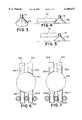
- FIG. 1is a top view showing a wafer in a first holding position (A)
- FIG. 2is top view on a wafer in a second holding position (B)
- FIG. 3is a perspective view of one embodiment of a guiding means
- FIG. 4is a sectional view of a wafer in a holding position onto one guiding means
- FIG. 5is a sectional view of a wafer in a gripping position onto one guiding means
- FIG. 6is a top view showing a wafer in an apparatus of a different embodiment in a first holding position.
- FIG. 7is a top view showing a wafer in a second holding position.
- FIG. 8is a view in cross-section showing an optional tongue and groove arrangement for guiding a first carrier 10 along a second carrier 20.
- FIG. 9is a view in side elevation illustrating guiding pins positioned near the free end of the inventive apparatus being shorter in height than the guiding pins positioned closer to an activating robot, in accordance with one embodiment of the invention.
- FIG. 1is a partial top view on an apparatus for handling and transporting a wafer.
- Carrier 10It comprises a plate like first carrier 10 of rectangular shape.
- Carrier 10is equipped with four guiding pins 12.1, 12.2, 12.3 and 12.4. Guiding pins 12.1 and 12.2. are arranged close to the corner regions at a free end 14a and guiding pins 12.3 and 12.4 are arranged opposite to each other at a distance a from said guiding pins 12.1, 12.2 close to side walls 16 of said carrier 10.
- Distance ais a bit larger than diameter w of a wafer 30 to be handled, although this feature is of course not imperative.
- carrier 10is coupled to a robot 40 via a telescope arm 50.
- Carrier 10is about two millimeters thick and contains gas channels (not shown), coupled at one end to a gas supply line (not shown) and running out at their other end in holes 18 in a top surface of carrier 10.
- a second carrier 20is--in its top view--U-shaped and presents as well a thickness of about two millimeters. It comprises two side arms 22s, running parallel to the side walls 16 of carrier 10 and a connecting arm 22c at its free end 24a.
- guiding pins 26.1, 26.2, 26.3 and 26.4extend perpendicular from a top surface of carrier 20.
- Guiding pins 26.3 and 26.4are arranged relatively close to the free end 24a while guiding pins 26.1 and 26.2 are placed at a distance b from said pins 26.3, 26.4. In this embodiment distance b is smaller than distance a.
- Carrier 20is fixedly secured to a "static" part 52 of said telescope arm 50.
- All guiding pinsare shaped according to FIG. 3, i.e. with a frustroconical basic part bp and a cylindrical top part tp.
- pins 12.1, 12.2; 26.1, 26.2belong to a first set while pins 12.3, 12.4; 26.3, 26.4 belong to a second set.
- carrier 10For loading a wafer from a cassette said carrier 10 is put in a position according to which its free end 14a is placed at a distance to the free end 24a of carrier 20.
- robot 40 carriers 10, 20are then positioned between two adjacent wafers in a wafer cassette (not shown).
- the assemblyis moved so that it enters the space between two adjacent wafers.
- the end effector assemblydoes not touch the surfaces of either wafer during this step.
- the moveable carrier 10is transferred by telescope arm 50 in a position shown in FIG. 1 (to the left) according to which the outer edge of wafer 30 gets in contact with the cylindrical surfaces of the upper parts (tp) of guiding members 12.3, 12.4; 26.3, 26.4, which now define a gripping position A.
- a gas like nitrogenmay be fed via holes 18, 28 into the space between the top surface of carrier 10 and the bottom surface of wafer 30, thereby forming an air cushion, onto which wafer 30 is hold in place without any contact areas because of the so called Bernoulli effect. Details insofar may be taken from U.S. Pat. No. 4,002,254.
- FIG. 5shows a wafer 30 being in contact at its outer edge with the top part (tp) of a guiding pin. Obviously wafer 30 is correspondingly gripped by the other three guiding pins of the corresponding set. In this particular position the assembly may be turned at any angle after taken off the corresponding cassette and for this purpose part 52 of telescope arm 50 is arranged rotatably.
- FIG. 2shows the assembly in a position for transporting a fresh wafer 30 into a cassette.
- wafer 30is held in position by guiding pins 12.1, 12,2; 26.1, 26.2 (second set) in the same way as disclosed according to the assembly position of FIG. 1.
- the two sets of guiding pins 12.1, 12.2; 26.1, 26.2 and 12.3, 12.4; 26.3, 26.4respectively serve to provide two independent holding positions for different wafers 30.
- different contact pointsmay be used for example for loading and unloading of a wafer and by this means any contaminations at one or more guiding pins of one set do not effect handling and transport of another wafer 30 with the other set of guiding pins.
- Carrier 10may be provided with tongues or grooves along its lateral outer side walls, and carrier 20 may be provided with corresponding grooves or tongues along its corresponding inner side walls. This optional feature is illustrated in FIG. 8, with carrier 10 being guided with its tongues along the corresponding grooves of carrier 20.
- the guiding pins positioned near the free end of the apparatusmay be shorter in height than the guiding pins positioned closer to the robot 40, as illustrated in FIG. 9.
- FIG. 6 and 7describe another version of an apparatus, comprising a first carrier 100 of flat, small and long shape, running parallel to a second carrier 200 of approximately same shape.
- Each carrier 100 and 200respectively are equipped with two guiding wings 120.1, 120.2 and 220.1, 220.2 respectively wherein wings 120.1, 220.1 belong to a first functional set while wings 120.2 and 220.2 create a second functional set of guiding means.
- Each wingis designed as a segment of a circle on its face facing the corresponding wing, so that the two wings 120.1, 220.1 of one set may hold and/or grip a wafer 300 in a first position (FIG. 6) and the other two wings 120.2, 220.2 of the second set are arranged as to hold or grip the wafer 300 in a separate second position (FIG. 7).
- both carriers 100, 200are moveable in a longitudinal direction (via corresponding tooth shaped side walls and corresponding tooth shaped wheels) to transfer the apparatus in the holding position wanted.
- the shape of the carrieris not limited to the shape as disclosed in the figures.
- carrier 20may be divided in two parts, each similar to side arms 22s.
- carrier 10may be divided into two arms, each being provided with two guiding pins (12.1, 12.3 and 12.2, 12.4 respectively).
- Another modificationmay provide a carrier 10 much smaller than that shown in FIGS. 1, 2, running in the middle between side arms 22s of carrier 20 and provided only with two guiding pins, one of each belonging to one set of guiding pins.
Landscapes
- Engineering & Computer Science (AREA)
- Robotics (AREA)
- Physics & Mathematics (AREA)
- Condensed Matter Physics & Semiconductors (AREA)
- General Physics & Mathematics (AREA)
- Manufacturing & Machinery (AREA)
- Computer Hardware Design (AREA)
- Microelectronics & Electronic Packaging (AREA)
- Power Engineering (AREA)
- Mechanical Engineering (AREA)
- Container, Conveyance, Adherence, Positioning, Of Wafer (AREA)
Abstract
Description
Claims (6)
Priority Applications (1)
| Application Number | Priority Date | Filing Date | Title |
|---|---|---|---|
| US09/086,980US6109677A (en) | 1998-05-28 | 1998-05-28 | Apparatus for handling and transporting plate like substrates |
Applications Claiming Priority (1)
| Application Number | Priority Date | Filing Date | Title |
|---|---|---|---|
| US09/086,980US6109677A (en) | 1998-05-28 | 1998-05-28 | Apparatus for handling and transporting plate like substrates |
Publications (1)
| Publication Number | Publication Date |
|---|---|
| US6109677Atrue US6109677A (en) | 2000-08-29 |
Family
ID=22202111
Family Applications (1)
| Application Number | Title | Priority Date | Filing Date |
|---|---|---|---|
| US09/086,980Expired - Fee RelatedUS6109677A (en) | 1998-05-28 | 1998-05-28 | Apparatus for handling and transporting plate like substrates |
Country Status (1)
| Country | Link |
|---|---|
| US (1) | US6109677A (en) |
Cited By (67)
| Publication number | Priority date | Publication date | Assignee | Title |
|---|---|---|---|---|
| US20030031549A1 (en)* | 2001-07-13 | 2003-02-13 | Berger Alexander J. | Alignment of semiconductor wafers and other articles |
| US20030082042A1 (en)* | 2001-07-13 | 2003-05-01 | Woodruff Daniel J. | End-effectors for handling microelectronic workpieces |
| US20030085582A1 (en)* | 2001-07-13 | 2003-05-08 | Woodruff Daniel J. | End-effectors for handling microelectronic workpieces |
| US6615113B2 (en) | 2001-07-13 | 2003-09-02 | Tru-Si Technologies, Inc. | Articles holders with sensors detecting a type of article held by the holder |
| US20030173790A1 (en)* | 2002-03-15 | 2003-09-18 | Hartog Edwin Den | Two level end effector |
| US6631935B1 (en)* | 2000-08-04 | 2003-10-14 | Tru-Si Technologies, Inc. | Detection and handling of semiconductor wafer and wafer-like objects |
| US6638004B2 (en) | 2001-07-13 | 2003-10-28 | Tru-Si Technologies, Inc. | Article holders and article positioning methods |
| US6676761B2 (en) | 2000-07-20 | 2004-01-13 | Applied Materials, Inc. | Method and apparatus for dechucking a substrate |
| US20040039486A1 (en)* | 1998-12-02 | 2004-02-26 | Paul Bacchi | Specimen sensing and edge gripping end effector |
| US6752585B2 (en) | 2001-06-13 | 2004-06-22 | Applied Materials Inc | Method and apparatus for transferring a semiconductor substrate |
| US20050006916A1 (en)* | 2003-06-27 | 2005-01-13 | Mattson Technology, Inc. | Endeffectors for handling semiconductor wafers |
| US20050155823A1 (en)* | 2002-02-25 | 2005-07-21 | Tsutomu Hiroki | Substrate support mechanism for semiconductor processing system |
| EP1566244A1 (en)* | 2004-02-20 | 2005-08-24 | Integrated Dynamics Engineering GmbH | Robot-guidance assembly for providing a precision motion of an object |
| US20050255244A1 (en)* | 2002-11-18 | 2005-11-17 | Applied Materials, Inc. | Lifting glass substrate without center lift pins |
| US20060005770A1 (en)* | 2004-07-09 | 2006-01-12 | Robin Tiner | Independently moving substrate supports |
| US20060011680A1 (en)* | 2004-07-09 | 2006-01-19 | Cook Clifton L | Hooded holster |
| US20060040111A1 (en)* | 2004-08-20 | 2006-02-23 | Dolechek Kert L | Process chamber and system for thinning a semiconductor workpiece |
| US20060040467A1 (en)* | 2004-08-20 | 2006-02-23 | Dolechek Kert L | Process and apparatus for thinning a semiconductor workpiece |
| US20060043750A1 (en)* | 2004-07-09 | 2006-03-02 | Paul Wirth | End-effectors for handling microfeature workpieces |
| US20060046499A1 (en)* | 2004-08-20 | 2006-03-02 | Dolechek Kert L | Apparatus for use in thinning a semiconductor workpiece |
| US20060045722A1 (en)* | 2004-06-22 | 2006-03-02 | Dainippon Screen Mfg. Co., Ltd. | Substrate reversing device, substrate transporting device, substrate processing device, substrate reversing method, substrate transporting method and substrate processing method |
| US20060118515A1 (en)* | 2004-08-20 | 2006-06-08 | Semitool, Inc. | Process For Thinning A Semiconductor Workpiece |
| US20060284434A1 (en)* | 2005-06-20 | 2006-12-21 | Yang Jong A | Substrate conveyance device for fabrication of liquid crystal display device |
| US20070014656A1 (en)* | 2002-07-11 | 2007-01-18 | Harris Randy A | End-effectors and associated control and guidance systems and methods |
| US20070020080A1 (en)* | 2004-07-09 | 2007-01-25 | Paul Wirth | Transfer devices and methods for handling microfeature workpieces within an environment of a processing machine |
| US20070108650A1 (en)* | 2005-06-27 | 2007-05-17 | Mirchandani Prakash K | Injection molding fabrication method |
| US7354649B2 (en) | 2004-08-20 | 2008-04-08 | Semitool, Inc. | Semiconductor workpiece |
| US20080166210A1 (en)* | 2007-01-05 | 2008-07-10 | Applied Materials, Inc. | Supinating cartesian robot blade |
| US20080213076A1 (en)* | 2007-03-02 | 2008-09-04 | Stephen Hanson | Edge grip end effector |
| US20090067956A1 (en)* | 2004-12-22 | 2009-03-12 | Tetsuya Ishikawa | Cluster tool architecture for processing a substrate |
| US7570876B2 (en) | 2003-08-20 | 2009-08-04 | Asm International N.V. | Method and system for loading substrate supports into a substrate holder |
| US7651306B2 (en) | 2004-12-22 | 2010-01-26 | Applied Materials, Inc. | Cartesian robot cluster tool architecture |
| US7798764B2 (en) | 2005-12-22 | 2010-09-21 | Applied Materials, Inc. | Substrate processing sequence in a cartesian robot cluster tool |
| US7819079B2 (en) | 2004-12-22 | 2010-10-26 | Applied Materials, Inc. | Cartesian cluster tool configuration for lithography type processes |
| US8087324B2 (en) | 2004-04-28 | 2012-01-03 | Tdy Industries, Inc. | Cast cones and other components for earth-boring tools and related methods |
| WO2011138703A3 (en)* | 2010-05-03 | 2012-01-12 | Memc Electronic Materials, Inc. | Wafer support ring |
| US20120128457A1 (en)* | 2010-11-24 | 2012-05-24 | Taiwan Semiconductor Manufacturing Company, Ltd. | Reconfigurable Guide Pin Design for Centering Wafers Having Different Sizes |
| US8201610B2 (en) | 2009-06-05 | 2012-06-19 | Baker Hughes Incorporated | Methods for manufacturing downhole tools and downhole tool parts |
| WO2012094470A3 (en)* | 2011-01-05 | 2012-09-13 | Electro Scientific Industries, Inc. | Apparatus and method for handling a substrate |
| US8272816B2 (en) | 2009-05-12 | 2012-09-25 | TDY Industries, LLC | Composite cemented carbide rotary cutting tools and rotary cutting tool blanks |
| CN102935942A (en)* | 2011-08-16 | 2013-02-20 | 中芯国际集成电路制造(北京)有限公司 | Electronic control manipulator |
| US20130051967A1 (en)* | 2011-08-26 | 2013-02-28 | Ryo Muramoto | Substrate inverting apparatus, substrate handling method, and substrate processing apparatus |
| US8459380B2 (en) | 2008-08-22 | 2013-06-11 | TDY Industries, LLC | Earth-boring bits and other parts including cemented carbide |
| US8490674B2 (en) | 2010-05-20 | 2013-07-23 | Baker Hughes Incorporated | Methods of forming at least a portion of earth-boring tools |
| US20140017042A1 (en)* | 2012-07-10 | 2014-01-16 | Lam Research Corporation | End effector having multiple-position contact points |
| US8647561B2 (en) | 2005-08-18 | 2014-02-11 | Kennametal Inc. | Composite cutting inserts and methods of making the same |
| US8697258B2 (en) | 2006-10-25 | 2014-04-15 | Kennametal Inc. | Articles having improved resistance to thermal cracking |
| US8789625B2 (en) | 2006-04-27 | 2014-07-29 | Kennametal Inc. | Modular fixed cutter earth-boring bits, modular fixed cutter earth-boring bit bodies, and related methods |
| US8790439B2 (en) | 2008-06-02 | 2014-07-29 | Kennametal Inc. | Composite sintered powder metal articles |
| US20140219764A1 (en)* | 2013-02-04 | 2014-08-07 | Spintrac Systems, Inc. | Centering guide for wafers of different sizes |
| US8800848B2 (en) | 2011-08-31 | 2014-08-12 | Kennametal Inc. | Methods of forming wear resistant layers on metallic surfaces |
| US20140262979A1 (en)* | 2013-03-14 | 2014-09-18 | Anthony C. Bonora | Tray Engine and Methods for Transferring Trays To and From Tools and in Sorters |
| US8905117B2 (en) | 2010-05-20 | 2014-12-09 | Baker Hughes Incoporated | Methods of forming at least a portion of earth-boring tools, and articles formed by such methods |
| US8978734B2 (en) | 2010-05-20 | 2015-03-17 | Baker Hughes Incorporated | Methods of forming at least a portion of earth-boring tools, and articles formed by such methods |
| US9016406B2 (en) | 2011-09-22 | 2015-04-28 | Kennametal Inc. | Cutting inserts for earth-boring bits |
| US9266171B2 (en) | 2009-07-14 | 2016-02-23 | Kennametal Inc. | Grinding roll including wear resistant working surface |
| US9428822B2 (en) | 2004-04-28 | 2016-08-30 | Baker Hughes Incorporated | Earth-boring tools and components thereof including material having hard phase in a metallic binder, and metallic binder compositions for use in forming such tools and components |
| US9643236B2 (en) | 2009-11-11 | 2017-05-09 | Landis Solutions Llc | Thread rolling die and method of making same |
| US20180330940A1 (en)* | 2011-06-23 | 2018-11-15 | Brooks Automation Gmbh | Semiconductor cleaner systems and methods |
| US10373858B2 (en) | 2016-04-06 | 2019-08-06 | Lam Research Corporation | Chuck for edge bevel removal and method for centering a wafer prior to edge bevel removal |
| US20190252235A1 (en)* | 2018-02-15 | 2019-08-15 | Applied Materials, Inc. | Apparatus for handling various sized substrates |
| CN111868907A (en)* | 2018-03-07 | 2020-10-30 | 东京毅力科创株式会社 | Horizontal substrate boat |
| US20210252716A1 (en)* | 2018-06-29 | 2021-08-19 | Kawasaki Jukogyo Kabushiki Kaisha | Substrate transfer device and method of operating the same |
| US11107722B2 (en)* | 2017-05-11 | 2021-08-31 | Rorze Corporation | Thin-plate substrate holding finger and transfer robot provided with said finger |
| WO2021194974A1 (en)* | 2020-03-23 | 2021-09-30 | Applied Materials, Inc. | Substrate processing system carrier |
| US20220051928A1 (en)* | 2020-08-17 | 2022-02-17 | Tokyo Electron Limited | Transfer device, transfer system, and end effector |
| US20220073287A1 (en)* | 2018-10-08 | 2022-03-10 | Becton Dickinson Rowa Germany Gmbh | Operating device for placing or retrieving bottle-like piece goods |
Citations (9)
| Publication number | Priority date | Publication date | Assignee | Title |
|---|---|---|---|---|
| US3950024A (en)* | 1975-01-13 | 1976-04-13 | James W. Smith | Apparatus for carrying disc-shaped articles |
| US4813732A (en)* | 1985-03-07 | 1989-03-21 | Epsilon Technology, Inc. | Apparatus and method for automated wafer handling |
| US4892455A (en)* | 1987-05-21 | 1990-01-09 | Hine Derek L | Wafer alignment and transport mechanism |
| US4971512A (en)* | 1987-12-18 | 1990-11-20 | Korea Electronics And Telecommunications Research Institute | Transport device for wafers of variable diameter |
| US5022695A (en)* | 1989-01-30 | 1991-06-11 | Texas Instruments Incorporated | Semiconductor slice holder |
| US5100285A (en)* | 1989-05-08 | 1992-03-31 | Balzers Aktiengesellschaft | Supporting and transport apparatus |
| US5484252A (en)* | 1993-02-22 | 1996-01-16 | Seiko Instruments Inc. | Sample holding apparatus |
| US5700046A (en)* | 1995-09-13 | 1997-12-23 | Silicon Valley Group, Inc. | Wafer gripper |
| US5711647A (en)* | 1994-10-17 | 1998-01-27 | Aesop, Inc. | Method of and apparatus for locating and orientating a part on a gripper and transferring it to a tool while maintaining location and orientation on the tool |
- 1998
- 1998-05-28USUS09/086,980patent/US6109677A/ennot_activeExpired - Fee Related
Patent Citations (9)
| Publication number | Priority date | Publication date | Assignee | Title |
|---|---|---|---|---|
| US3950024A (en)* | 1975-01-13 | 1976-04-13 | James W. Smith | Apparatus for carrying disc-shaped articles |
| US4813732A (en)* | 1985-03-07 | 1989-03-21 | Epsilon Technology, Inc. | Apparatus and method for automated wafer handling |
| US4892455A (en)* | 1987-05-21 | 1990-01-09 | Hine Derek L | Wafer alignment and transport mechanism |
| US4971512A (en)* | 1987-12-18 | 1990-11-20 | Korea Electronics And Telecommunications Research Institute | Transport device for wafers of variable diameter |
| US5022695A (en)* | 1989-01-30 | 1991-06-11 | Texas Instruments Incorporated | Semiconductor slice holder |
| US5100285A (en)* | 1989-05-08 | 1992-03-31 | Balzers Aktiengesellschaft | Supporting and transport apparatus |
| US5484252A (en)* | 1993-02-22 | 1996-01-16 | Seiko Instruments Inc. | Sample holding apparatus |
| US5711647A (en)* | 1994-10-17 | 1998-01-27 | Aesop, Inc. | Method of and apparatus for locating and orientating a part on a gripper and transferring it to a tool while maintaining location and orientation on the tool |
| US5700046A (en)* | 1995-09-13 | 1997-12-23 | Silicon Valley Group, Inc. | Wafer gripper |
Cited By (150)
| Publication number | Priority date | Publication date | Assignee | Title |
|---|---|---|---|---|
| US20040039486A1 (en)* | 1998-12-02 | 2004-02-26 | Paul Bacchi | Specimen sensing and edge gripping end effector |
| US6898487B2 (en) | 1998-12-02 | 2005-05-24 | Newport Corporation | Specimen sensing and edge gripping end effector |
| US7160392B2 (en) | 2000-07-20 | 2007-01-09 | Applied Materials, Inc. | Method for dechucking a substrate |
| US20070062454A1 (en)* | 2000-07-20 | 2007-03-22 | Applied Materials, Inc. | Method for dechucking a substrate |
| US20040089239A1 (en)* | 2000-07-20 | 2004-05-13 | Applied Materials, Inc. | Method for dechucking a substrate |
| US6676761B2 (en) | 2000-07-20 | 2004-01-13 | Applied Materials, Inc. | Method and apparatus for dechucking a substrate |
| US7144056B2 (en) | 2000-08-04 | 2006-12-05 | Tru-Si Technologies, Inc. | Detection and handling of semiconductor wafers and wafers-like objects |
| US6631935B1 (en)* | 2000-08-04 | 2003-10-14 | Tru-Si Technologies, Inc. | Detection and handling of semiconductor wafer and wafer-like objects |
| US6688662B2 (en) | 2000-08-04 | 2004-02-10 | Tru-Si Technologies, Inc. | Detection and handling of semiconductor wafers and wafer-like objects |
| US20040150237A1 (en)* | 2000-08-04 | 2004-08-05 | Casarotti Sean A. | Detection and handling of semiconductor wafers and wafer-like objects |
| US7104579B2 (en) | 2000-08-04 | 2006-09-12 | Tru-Si Technologies Inc. | Detection and handling of semiconductor wafers and wafer-like objects |
| US7153088B2 (en) | 2001-06-13 | 2006-12-26 | Applied Materials, Inc. | Method and apparatus for transferring a semiconductor substrate |
| US20040219001A1 (en)* | 2001-06-13 | 2004-11-04 | Applied Materials, Inc. | Method and apparatus for transferring a semiconductor substrate |
| US6752585B2 (en) | 2001-06-13 | 2004-06-22 | Applied Materials Inc | Method and apparatus for transferring a semiconductor substrate |
| US20050004701A1 (en)* | 2001-07-13 | 2005-01-06 | Berger Alexander J. | Alignment of semiconductor wafers and other articles |
| US20030085582A1 (en)* | 2001-07-13 | 2003-05-08 | Woodruff Daniel J. | End-effectors for handling microelectronic workpieces |
| US7281741B2 (en) | 2001-07-13 | 2007-10-16 | Semitool, Inc. | End-effectors for handling microelectronic workpieces |
| US7052229B2 (en) | 2001-07-13 | 2006-05-30 | Tru-Si Technologies Inc. | Alignment of semiconductor wafers and other articles |
| US6665583B2 (en) | 2001-07-13 | 2003-12-16 | Tru-Si Technologies, Inc. | Article holders with sensors detecting a type of article held by the holder |
| US7027894B2 (en) | 2001-07-13 | 2006-04-11 | Tru-Si Technologies, Inc. | Article holders with sensors detecting a type of article held by the holder |
| US6638004B2 (en) | 2001-07-13 | 2003-10-28 | Tru-Si Technologies, Inc. | Article holders and article positioning methods |
| US7334826B2 (en)* | 2001-07-13 | 2008-02-26 | Semitool, Inc. | End-effectors for handling microelectronic wafers |
| US6935830B2 (en) | 2001-07-13 | 2005-08-30 | Tru-Si Technologies, Inc. | Alignment of semiconductor wafers and other articles |
| US6948898B2 (en) | 2001-07-13 | 2005-09-27 | Tru-Si Technologies, Inc. | Alignment of semiconductor wafers and other articles |
| US20030082042A1 (en)* | 2001-07-13 | 2003-05-01 | Woodruff Daniel J. | End-effectors for handling microelectronic workpieces |
| US6615113B2 (en) | 2001-07-13 | 2003-09-02 | Tru-Si Technologies, Inc. | Articles holders with sensors detecting a type of article held by the holder |
| US20030031549A1 (en)* | 2001-07-13 | 2003-02-13 | Berger Alexander J. | Alignment of semiconductor wafers and other articles |
| US20040049318A1 (en)* | 2001-07-13 | 2004-03-11 | Kretz Frank E. | Article holders with sensors detecting a type of article held by the holder |
| US7857569B2 (en) | 2002-02-25 | 2010-12-28 | Tokyo Electron Limited | Semiconductor processing system |
| US20050155823A1 (en)* | 2002-02-25 | 2005-07-21 | Tsutomu Hiroki | Substrate support mechanism for semiconductor processing system |
| US7104578B2 (en) | 2002-03-15 | 2006-09-12 | Asm International N.V. | Two level end effector |
| US20030173790A1 (en)* | 2002-03-15 | 2003-09-18 | Hartog Edwin Den | Two level end effector |
| US20070014656A1 (en)* | 2002-07-11 | 2007-01-18 | Harris Randy A | End-effectors and associated control and guidance systems and methods |
| US20050255244A1 (en)* | 2002-11-18 | 2005-11-17 | Applied Materials, Inc. | Lifting glass substrate without center lift pins |
| US8622451B2 (en) | 2003-06-27 | 2014-01-07 | Mattson Technology, Inc. | Endeffectors for handling semiconductor wafers |
| US8109549B2 (en) | 2003-06-27 | 2012-02-07 | Mattson Technology, Inc. | Endeffectors for handling semiconductor wafers |
| US7654596B2 (en) | 2003-06-27 | 2010-02-02 | Mattson Technology, Inc. | Endeffectors for handling semiconductor wafers |
| US20100096869A1 (en)* | 2003-06-27 | 2010-04-22 | Mattson Thermal Products Gmbh | Endeffectors for handling semiconductor wafers |
| US20050006916A1 (en)* | 2003-06-27 | 2005-01-13 | Mattson Technology, Inc. | Endeffectors for handling semiconductor wafers |
| US7570876B2 (en) | 2003-08-20 | 2009-08-04 | Asm International N.V. | Method and system for loading substrate supports into a substrate holder |
| US7264436B2 (en) | 2004-02-20 | 2007-09-04 | Integrated Dynamics Engineering Gmbh | Robot-guidance assembly for providing a precision motion of an object |
| US20050183533A1 (en)* | 2004-02-20 | 2005-08-25 | Integrated Dynamics Engineering Gmbh | Robot-guidance assembly for providing a precision motion of an object |
| EP1566244A1 (en)* | 2004-02-20 | 2005-08-24 | Integrated Dynamics Engineering GmbH | Robot-guidance assembly for providing a precision motion of an object |
| US9428822B2 (en) | 2004-04-28 | 2016-08-30 | Baker Hughes Incorporated | Earth-boring tools and components thereof including material having hard phase in a metallic binder, and metallic binder compositions for use in forming such tools and components |
| US8403080B2 (en) | 2004-04-28 | 2013-03-26 | Baker Hughes Incorporated | Earth-boring tools and components thereof including material having hard phase in a metallic binder, and metallic binder compositions for use in forming such tools and components |
| US10167673B2 (en) | 2004-04-28 | 2019-01-01 | Baker Hughes Incorporated | Earth-boring tools and methods of forming tools including hard particles in a binder |
| US8087324B2 (en) | 2004-04-28 | 2012-01-03 | Tdy Industries, Inc. | Cast cones and other components for earth-boring tools and related methods |
| US7322787B2 (en)* | 2004-06-22 | 2008-01-29 | Dainippon Screen Mfg. Co., Ltd. | Devices and methods for reversing, transporting, and processing substrates |
| US20060045722A1 (en)* | 2004-06-22 | 2006-03-02 | Dainippon Screen Mfg. Co., Ltd. | Substrate reversing device, substrate transporting device, substrate processing device, substrate reversing method, substrate transporting method and substrate processing method |
| US20070020080A1 (en)* | 2004-07-09 | 2007-01-25 | Paul Wirth | Transfer devices and methods for handling microfeature workpieces within an environment of a processing machine |
| US20060005770A1 (en)* | 2004-07-09 | 2006-01-12 | Robin Tiner | Independently moving substrate supports |
| US20060011680A1 (en)* | 2004-07-09 | 2006-01-19 | Cook Clifton L | Hooded holster |
| US20060043750A1 (en)* | 2004-07-09 | 2006-03-02 | Paul Wirth | End-effectors for handling microfeature workpieces |
| US7354649B2 (en) | 2004-08-20 | 2008-04-08 | Semitool, Inc. | Semiconductor workpiece |
| US20060046499A1 (en)* | 2004-08-20 | 2006-03-02 | Dolechek Kert L | Apparatus for use in thinning a semiconductor workpiece |
| US7193295B2 (en) | 2004-08-20 | 2007-03-20 | Semitool, Inc. | Process and apparatus for thinning a semiconductor workpiece |
| US20060040467A1 (en)* | 2004-08-20 | 2006-02-23 | Dolechek Kert L | Process and apparatus for thinning a semiconductor workpiece |
| US7288489B2 (en) | 2004-08-20 | 2007-10-30 | Semitool, Inc. | Process for thinning a semiconductor workpiece |
| US20060040111A1 (en)* | 2004-08-20 | 2006-02-23 | Dolechek Kert L | Process chamber and system for thinning a semiconductor workpiece |
| US7625821B2 (en) | 2004-08-20 | 2009-12-01 | Semitool, Inc. | Process and apparatus for thinning a semiconductor workpiece |
| US20060118515A1 (en)* | 2004-08-20 | 2006-06-08 | Semitool, Inc. | Process For Thinning A Semiconductor Workpiece |
| US20060203419A1 (en)* | 2004-08-20 | 2006-09-14 | Semitool, Inc. | Process and apparatus for thinning a semiconductor workpiece |
| US8181596B2 (en) | 2004-12-22 | 2012-05-22 | Applied Materials, Inc. | Cluster tool architecture for processing a substrate |
| US8215262B2 (en) | 2004-12-22 | 2012-07-10 | Applied Materials, Inc. | Cluster tool architecture for processing a substrate |
| US7743728B2 (en) | 2004-12-22 | 2010-06-29 | Applied Materials, Inc. | Cluster tool architecture for processing a substrate |
| US8550031B2 (en) | 2004-12-22 | 2013-10-08 | Applied Materials, Inc. | Cluster tool architecture for processing a substrate |
| US7819079B2 (en) | 2004-12-22 | 2010-10-26 | Applied Materials, Inc. | Cartesian cluster tool configuration for lithography type processes |
| US7651306B2 (en) | 2004-12-22 | 2010-01-26 | Applied Materials, Inc. | Cartesian robot cluster tool architecture |
| US7925377B2 (en) | 2004-12-22 | 2011-04-12 | Applied Materials, Inc. | Cluster tool architecture for processing a substrate |
| US7694647B2 (en) | 2004-12-22 | 2010-04-13 | Applied Materials, Inc. | Cluster tool architecture for processing a substrate |
| US20090064929A1 (en)* | 2004-12-22 | 2009-03-12 | Tetsuya Ishikawa | Cluster tool architecture for processing a substrate |
| US8911193B2 (en) | 2004-12-22 | 2014-12-16 | Applied Materials, Inc. | Substrate processing sequence in a cartesian robot cluster tool |
| US20090067956A1 (en)* | 2004-12-22 | 2009-03-12 | Tetsuya Ishikawa | Cluster tool architecture for processing a substrate |
| US8146530B2 (en) | 2004-12-22 | 2012-04-03 | Applied Materials, Inc. | Cluster tool architecture for processing a substrate |
| US7401828B2 (en)* | 2005-06-20 | 2008-07-22 | Lg Display Co., Ltd. | Substrate conveyance device for fabrication of liquid crystal display device |
| US20060284434A1 (en)* | 2005-06-20 | 2006-12-21 | Yang Jong A | Substrate conveyance device for fabrication of liquid crystal display device |
| US8808591B2 (en) | 2005-06-27 | 2014-08-19 | Kennametal Inc. | Coextrusion fabrication method |
| US8637127B2 (en) | 2005-06-27 | 2014-01-28 | Kennametal Inc. | Composite article with coolant channels and tool fabrication method |
| US20070108650A1 (en)* | 2005-06-27 | 2007-05-17 | Mirchandani Prakash K | Injection molding fabrication method |
| US8318063B2 (en) | 2005-06-27 | 2012-11-27 | TDY Industries, LLC | Injection molding fabrication method |
| US8647561B2 (en) | 2005-08-18 | 2014-02-11 | Kennametal Inc. | Composite cutting inserts and methods of making the same |
| US8066466B2 (en) | 2005-12-22 | 2011-11-29 | Applied Materials, Inc. | Substrate processing sequence in a Cartesian robot cluster tool |
| US7798764B2 (en) | 2005-12-22 | 2010-09-21 | Applied Materials, Inc. | Substrate processing sequence in a cartesian robot cluster tool |
| US8789625B2 (en) | 2006-04-27 | 2014-07-29 | Kennametal Inc. | Modular fixed cutter earth-boring bits, modular fixed cutter earth-boring bit bodies, and related methods |
| US8841005B2 (en) | 2006-10-25 | 2014-09-23 | Kennametal Inc. | Articles having improved resistance to thermal cracking |
| US8697258B2 (en) | 2006-10-25 | 2014-04-15 | Kennametal Inc. | Articles having improved resistance to thermal cracking |
| US20080166210A1 (en)* | 2007-01-05 | 2008-07-10 | Applied Materials, Inc. | Supinating cartesian robot blade |
| US20080213076A1 (en)* | 2007-03-02 | 2008-09-04 | Stephen Hanson | Edge grip end effector |
| US8790439B2 (en) | 2008-06-02 | 2014-07-29 | Kennametal Inc. | Composite sintered powder metal articles |
| US8459380B2 (en) | 2008-08-22 | 2013-06-11 | TDY Industries, LLC | Earth-boring bits and other parts including cemented carbide |
| US8858870B2 (en) | 2008-08-22 | 2014-10-14 | Kennametal Inc. | Earth-boring bits and other parts including cemented carbide |
| US8272816B2 (en) | 2009-05-12 | 2012-09-25 | TDY Industries, LLC | Composite cemented carbide rotary cutting tools and rotary cutting tool blanks |
| US9435010B2 (en) | 2009-05-12 | 2016-09-06 | Kennametal Inc. | Composite cemented carbide rotary cutting tools and rotary cutting tool blanks |
| US8201610B2 (en) | 2009-06-05 | 2012-06-19 | Baker Hughes Incorporated | Methods for manufacturing downhole tools and downhole tool parts |
| US8464814B2 (en) | 2009-06-05 | 2013-06-18 | Baker Hughes Incorporated | Systems for manufacturing downhole tools and downhole tool parts |
| US8869920B2 (en) | 2009-06-05 | 2014-10-28 | Baker Hughes Incorporated | Downhole tools and parts and methods of formation |
| US8317893B2 (en) | 2009-06-05 | 2012-11-27 | Baker Hughes Incorporated | Downhole tool parts and compositions thereof |
| US9266171B2 (en) | 2009-07-14 | 2016-02-23 | Kennametal Inc. | Grinding roll including wear resistant working surface |
| US9643236B2 (en) | 2009-11-11 | 2017-05-09 | Landis Solutions Llc | Thread rolling die and method of making same |
| WO2011138703A3 (en)* | 2010-05-03 | 2012-01-12 | Memc Electronic Materials, Inc. | Wafer support ring |
| US8420554B2 (en) | 2010-05-03 | 2013-04-16 | Memc Electronic Materials, Inc. | Wafer support ring |
| US9790745B2 (en) | 2010-05-20 | 2017-10-17 | Baker Hughes Incorporated | Earth-boring tools comprising eutectic or near-eutectic compositions |
| US8905117B2 (en) | 2010-05-20 | 2014-12-09 | Baker Hughes Incoporated | Methods of forming at least a portion of earth-boring tools, and articles formed by such methods |
| US8490674B2 (en) | 2010-05-20 | 2013-07-23 | Baker Hughes Incorporated | Methods of forming at least a portion of earth-boring tools |
| US10603765B2 (en) | 2010-05-20 | 2020-03-31 | Baker Hughes, a GE company, LLC. | Articles comprising metal, hard material, and an inoculant, and related methods |
| US9687963B2 (en) | 2010-05-20 | 2017-06-27 | Baker Hughes Incorporated | Articles comprising metal, hard material, and an inoculant |
| US8978734B2 (en) | 2010-05-20 | 2015-03-17 | Baker Hughes Incorporated | Methods of forming at least a portion of earth-boring tools, and articles formed by such methods |
| CN107481967A (en)* | 2010-11-24 | 2017-12-15 | 台湾积体电路制造股份有限公司 | For the different wafer of size restructural pilot pin placed in the middle to be designed |
| US9099515B2 (en) | 2010-11-24 | 2015-08-04 | Taiwan Semiconductor Manufacturing Company, Ltd. | Reconfigurable guide pin design for centering wafers having different sizes |
| US20120128457A1 (en)* | 2010-11-24 | 2012-05-24 | Taiwan Semiconductor Manufacturing Company, Ltd. | Reconfigurable Guide Pin Design for Centering Wafers Having Different Sizes |
| US8567837B2 (en)* | 2010-11-24 | 2013-10-29 | Taiwan Semiconductor Manufacturing Company, Ltd. | Reconfigurable guide pin design for centering wafers having different sizes |
| WO2012094470A3 (en)* | 2011-01-05 | 2012-09-13 | Electro Scientific Industries, Inc. | Apparatus and method for handling a substrate |
| JP2014503121A (en)* | 2011-01-05 | 2014-02-06 | エレクトロ サイエンティフィック インダストリーズ インコーポレーテッド | Substrate operating apparatus and method |
| US8702142B2 (en) | 2011-01-05 | 2014-04-22 | Electro Scientific Industries, Inc. | Apparatus and method for handling a substrate |
| CN103380493B (en)* | 2011-01-05 | 2016-04-13 | 伊雷克托科学工业股份有限公司 | Apparatus and methods for processing substrates |
| CN103380493A (en)* | 2011-01-05 | 2013-10-30 | 伊雷克托科学工业股份有限公司 | Apparatus and method for handling a substrate |
| US20180330940A1 (en)* | 2011-06-23 | 2018-11-15 | Brooks Automation Gmbh | Semiconductor cleaner systems and methods |
| US11152203B2 (en) | 2011-06-23 | 2021-10-19 | Brooks Automation (Germany) Gmbh | Semiconductor cleaner systems and methods |
| US10892155B2 (en)* | 2011-06-23 | 2021-01-12 | Brooks Automation (Germany) Gmbh | Semiconductor cleaner systems and methods |
| US8556318B2 (en)* | 2011-08-16 | 2013-10-15 | Semiconductor Manufacturing International (Beijing) Corporation | Electric-controlled operator |
| CN102935942A (en)* | 2011-08-16 | 2013-02-20 | 中芯国际集成电路制造(北京)有限公司 | Electronic control manipulator |
| CN102935942B (en)* | 2011-08-16 | 2015-03-04 | 中芯国际集成电路制造(北京)有限公司 | Electronic control manipulator |
| US20130051967A1 (en)* | 2011-08-26 | 2013-02-28 | Ryo Muramoto | Substrate inverting apparatus, substrate handling method, and substrate processing apparatus |
| CN102951445A (en)* | 2011-08-26 | 2013-03-06 | 大日本网屏制造株式会社 | Substrate inverting apparatus, substrate handling method, and substrate processing apparatus |
| CN102951445B (en)* | 2011-08-26 | 2015-10-07 | 斯克林集团公司 | Substrate reversing gear and substrate method of operation and substrate board treatment |
| US8800848B2 (en) | 2011-08-31 | 2014-08-12 | Kennametal Inc. | Methods of forming wear resistant layers on metallic surfaces |
| US9016406B2 (en) | 2011-09-22 | 2015-04-28 | Kennametal Inc. | Cutting inserts for earth-boring bits |
| US9214375B2 (en)* | 2012-07-10 | 2015-12-15 | Lam Research Corporation | End effector having multiple-position contact points |
| KR20140008502A (en)* | 2012-07-10 | 2014-01-21 | 램 리써치 코포레이션 | End effector having multiple-position contact points |
| US20140017042A1 (en)* | 2012-07-10 | 2014-01-16 | Lam Research Corporation | End effector having multiple-position contact points |
| US20140219764A1 (en)* | 2013-02-04 | 2014-08-07 | Spintrac Systems, Inc. | Centering guide for wafers of different sizes |
| CN105121309A (en)* | 2013-03-14 | 2015-12-02 | 布鲁克斯自动化公司 | Pallet motor for conveying pallets |
| US20140262979A1 (en)* | 2013-03-14 | 2014-09-18 | Anthony C. Bonora | Tray Engine and Methods for Transferring Trays To and From Tools and in Sorters |
| US9545724B2 (en)* | 2013-03-14 | 2017-01-17 | Brooks Automation, Inc. | Tray engine with slide attached to an end effector base |
| US10373858B2 (en) | 2016-04-06 | 2019-08-06 | Lam Research Corporation | Chuck for edge bevel removal and method for centering a wafer prior to edge bevel removal |
| US10971388B2 (en) | 2016-04-06 | 2021-04-06 | Lam Research Corporation | Chuck for edge bevel removal and method for centering a wafer prior to edge bevel removal |
| TWI765025B (en)* | 2017-05-11 | 2022-05-21 | 日商樂華股份有限公司 | Thin plate substrate-holding finger and transfer robot provided with this finger |
| US11107722B2 (en)* | 2017-05-11 | 2021-08-31 | Rorze Corporation | Thin-plate substrate holding finger and transfer robot provided with said finger |
| WO2019161026A1 (en)* | 2018-02-15 | 2019-08-22 | Applied Materials, Inc. | Apparatus for handling various sized substrates |
| US20190252235A1 (en)* | 2018-02-15 | 2019-08-15 | Applied Materials, Inc. | Apparatus for handling various sized substrates |
| US10930542B2 (en)* | 2018-02-15 | 2021-02-23 | Applied Materials, Inc. | Apparatus for handling various sized substrates |
| CN111868907A (en)* | 2018-03-07 | 2020-10-30 | 东京毅力科创株式会社 | Horizontal substrate boat |
| US20210252716A1 (en)* | 2018-06-29 | 2021-08-19 | Kawasaki Jukogyo Kabushiki Kaisha | Substrate transfer device and method of operating the same |
| US11839968B2 (en)* | 2018-06-29 | 2023-12-12 | Kawasaki Jukogyo Kabushiki Kaisha | Substrate transfer device and method of operating the same |
| US20220073287A1 (en)* | 2018-10-08 | 2022-03-10 | Becton Dickinson Rowa Germany Gmbh | Operating device for placing or retrieving bottle-like piece goods |
| US11713200B2 (en)* | 2018-10-08 | 2023-08-01 | Becton Dickinson Rowa Germany Gmbh | Operating device for placing or retrieving bottle-like piece goods |
| US12006164B2 (en) | 2018-10-08 | 2024-06-11 | Becton Dickinson Rowa Germany Gmbh | Operating device for placing or retrieving bottle-like piece goods |
| WO2021194974A1 (en)* | 2020-03-23 | 2021-09-30 | Applied Materials, Inc. | Substrate processing system carrier |
| US20220051928A1 (en)* | 2020-08-17 | 2022-02-17 | Tokyo Electron Limited | Transfer device, transfer system, and end effector |
| US12191188B2 (en)* | 2020-08-17 | 2025-01-07 | Tokyo Electron Limited | Transfer device, transfer system, and end effector |
Similar Documents
| Publication | Publication Date | Title |
|---|---|---|
| US6109677A (en) | Apparatus for handling and transporting plate like substrates | |
| US10434661B2 (en) | Workpiece support structures and apparatus for accessing same | |
| JP4743939B2 (en) | Method and apparatus for transporting a semiconductor substrate using an input module | |
| JP4230642B2 (en) | Substrate transport jig and substrate transport device | |
| TWI636858B (en) | Substrate transfer robot and substrate processing system | |
| KR101695434B1 (en) | System and methods for handling wafers | |
| KR100638942B1 (en) | Apparatus and Method for Processing Each Wafer | |
| JP6535187B2 (en) | Substrate transfer hand | |
| JP2010010718A (en) | Semiconductor substrate cleaning system | |
| KR20250048284A (en) | End effector and robot with end effector | |
| US6406359B1 (en) | Apparatus for transferring semiconductor substrates using an input module | |
| US20040179932A1 (en) | Robotic hand with multi-wafer end effector | |
| JPH11116046A (en) | Robot hand for wafer carrying robot | |
| JP5279554B2 (en) | Substrate processing equipment | |
| JP2010206041A (en) | Substrate processing apparatus | |
| JP7430074B2 (en) | Substrate holding device | |
| JPS61156749A (en) | Wafer flat plate type back side vacuum chuck | |
| JPS63111637A (en) | Wafer transfer processing equipment | |
| KR100583942B1 (en) | Fixing Device for Wafer for Double Sided Processing | |
| US20030051974A1 (en) | Automated semiconductor processing system | |
| JP2506379B2 (en) | Conveying method and conveying device | |
| JPH07142561A (en) | Wafer holder | |
| JPS63250130A (en) | Semiconductor wafer processing equipment | |
| KR970001884B1 (en) | Wafer cacett | |
| JPH11233588A5 (en) | Wafer processing apparatus and wafer processing method |
Legal Events
| Date | Code | Title | Description |
|---|---|---|---|
| AS | Assignment | Owner name:SEZ NORTH AMERICA, INC., ARIZONA Free format text:ASSIGNMENT OF ASSIGNORS INTEREST;ASSIGNOR:ANTHONY, KURT G.;REEL/FRAME:009243/0345 Effective date:19980527 | |
| AS | Assignment | Owner name:SEZ NORTH AMERICA, INC., ARIZONA Free format text:ASSIGNMENT OF ASSIGNORS INTEREST;ASSIGNOR:ANTHONY, KURT G.;REEL/FRAME:009417/0161 Effective date:19980527 | |
| FEPP | Fee payment procedure | Free format text:PAYOR NUMBER ASSIGNED (ORIGINAL EVENT CODE: ASPN); ENTITY STATUS OF PATENT OWNER: LARGE ENTITY Free format text:PAT HOLDER NO LONGER CLAIMS SMALL ENTITY STATUS, ENTITY STATUS SET TO UNDISCOUNTED (ORIGINAL EVENT CODE: STOL); ENTITY STATUS OF PATENT OWNER: LARGE ENTITY | |
| FPAY | Fee payment | Year of fee payment:4 | |
| FPAY | Fee payment | Year of fee payment:8 | |
| AS | Assignment | Owner name:LAM RESEARCH AG, AUSTRIA Free format text:ASSIGNMENT OF ASSIGNORS INTEREST;ASSIGNOR:SEZ AMERICA INC. (FORMERLY SEZ NORTH AMERICA INC.);REEL/FRAME:023134/0163 Effective date:20090819 | |
| REMI | Maintenance fee reminder mailed | ||
| LAPS | Lapse for failure to pay maintenance fees | ||
| STCH | Information on status: patent discontinuation | Free format text:PATENT EXPIRED DUE TO NONPAYMENT OF MAINTENANCE FEES UNDER 37 CFR 1.362 | |
| FP | Lapsed due to failure to pay maintenance fee | Effective date:20120829 |