US6107679A - Semiconductor device - Google Patents
Semiconductor deviceDownload PDFInfo
- Publication number
- US6107679A US6107679AUS09/200,964US20096498AUS6107679AUS 6107679 AUS6107679 AUS 6107679AUS 20096498 AUS20096498 AUS 20096498AUS 6107679 AUS6107679 AUS 6107679A
- Authority
- US
- United States
- Prior art keywords
- base material
- semiconductor device
- semiconductor
- portions
- solder resist
- Prior art date
- Legal status (The legal status is an assumption and is not a legal conclusion. Google has not performed a legal analysis and makes no representation as to the accuracy of the status listed.)
- Expired - Lifetime
Links
- 239000004065semiconductorSubstances0.000titleclaimsabstractdescription58
- 239000000463materialSubstances0.000claimsabstractdescription80
- 238000007789sealingMethods0.000claimsabstractdescription33
- 230000002093peripheral effectEffects0.000claimsabstractdescription8
- 229910000679solderInorganic materials0.000claimsdescription30
- 239000000853adhesiveSubstances0.000claimsdescription22
- 230000001070adhesive effectEffects0.000claimsdescription22
- 239000002245particleSubstances0.000claimsdescription8
- 239000011347resinSubstances0.000description21
- 229920005989resinPolymers0.000description21
- 238000000034methodMethods0.000description5
- 229910052751metalInorganic materials0.000description4
- 239000002184metalSubstances0.000description4
- 238000012986modificationMethods0.000description4
- 230000004048modificationEffects0.000description4
- 239000000945fillerSubstances0.000description3
- 239000004593EpoxySubstances0.000description2
- BQCADISMDOOEFD-UHFFFAOYSA-NSilverChemical compound[Ag]BQCADISMDOOEFD-UHFFFAOYSA-N0.000description1
- 239000002390adhesive tapeSubstances0.000description1
- 230000015572biosynthetic processEffects0.000description1
- 239000004020conductorSubstances0.000description1
- 238000007796conventional methodMethods0.000description1
- 238000011161developmentMethods0.000description1
- 238000007599dischargingMethods0.000description1
- 238000005553drillingMethods0.000description1
- 239000011521glassSubstances0.000description1
- 230000007257malfunctionEffects0.000description1
- 238000004382pottingMethods0.000description1
- 238000000926separation methodMethods0.000description1
- 229910052709silverInorganic materials0.000description1
- 239000004332silverSubstances0.000description1
- 239000000126substanceSubstances0.000description1
- 238000012546transferMethods0.000description1
Images


Classifications
- H—ELECTRICITY
- H01—ELECTRIC ELEMENTS
- H01L—SEMICONDUCTOR DEVICES NOT COVERED BY CLASS H10
- H01L24/00—Arrangements for connecting or disconnecting semiconductor or solid-state bodies; Methods or apparatus related thereto
- H01L24/93—Batch processes
- H01L24/95—Batch processes at chip-level, i.e. with connecting carried out on a plurality of singulated devices, i.e. on diced chips
- H01L24/97—Batch processes at chip-level, i.e. with connecting carried out on a plurality of singulated devices, i.e. on diced chips the devices being connected to a common substrate, e.g. interposer, said common substrate being separable into individual assemblies after connecting
- H—ELECTRICITY
- H01—ELECTRIC ELEMENTS
- H01L—SEMICONDUCTOR DEVICES NOT COVERED BY CLASS H10
- H01L23/00—Details of semiconductor or other solid state devices
- H01L23/12—Mountings, e.g. non-detachable insulating substrates
- H01L23/13—Mountings, e.g. non-detachable insulating substrates characterised by the shape
- H—ELECTRICITY
- H01—ELECTRIC ELEMENTS
- H01L—SEMICONDUCTOR DEVICES NOT COVERED BY CLASS H10
- H01L23/00—Details of semiconductor or other solid state devices
- H01L23/28—Encapsulations, e.g. encapsulating layers, coatings, e.g. for protection
- H01L23/31—Encapsulations, e.g. encapsulating layers, coatings, e.g. for protection characterised by the arrangement or shape
- H01L23/3107—Encapsulations, e.g. encapsulating layers, coatings, e.g. for protection characterised by the arrangement or shape the device being completely enclosed
- H01L23/3121—Encapsulations, e.g. encapsulating layers, coatings, e.g. for protection characterised by the arrangement or shape the device being completely enclosed a substrate forming part of the encapsulation
- H—ELECTRICITY
- H01—ELECTRIC ELEMENTS
- H01L—SEMICONDUCTOR DEVICES NOT COVERED BY CLASS H10
- H01L23/00—Details of semiconductor or other solid state devices
- H01L23/28—Encapsulations, e.g. encapsulating layers, coatings, e.g. for protection
- H01L23/31—Encapsulations, e.g. encapsulating layers, coatings, e.g. for protection characterised by the arrangement or shape
- H01L23/3107—Encapsulations, e.g. encapsulating layers, coatings, e.g. for protection characterised by the arrangement or shape the device being completely enclosed
- H01L23/3142—Sealing arrangements between parts, e.g. adhesion promotors
- H—ELECTRICITY
- H01—ELECTRIC ELEMENTS
- H01L—SEMICONDUCTOR DEVICES NOT COVERED BY CLASS H10
- H01L24/00—Arrangements for connecting or disconnecting semiconductor or solid-state bodies; Methods or apparatus related thereto
- H01L24/01—Means for bonding being attached to, or being formed on, the surface to be connected, e.g. chip-to-package, die-attach, "first-level" interconnects; Manufacturing methods related thereto
- H01L24/26—Layer connectors, e.g. plate connectors, solder or adhesive layers; Manufacturing methods related thereto
- H01L24/31—Structure, shape, material or disposition of the layer connectors after the connecting process
- H01L24/32—Structure, shape, material or disposition of the layer connectors after the connecting process of an individual layer connector
- H—ELECTRICITY
- H01—ELECTRIC ELEMENTS
- H01L—SEMICONDUCTOR DEVICES NOT COVERED BY CLASS H10
- H01L21/00—Processes or apparatus adapted for the manufacture or treatment of semiconductor or solid state devices or of parts thereof
- H01L21/02—Manufacture or treatment of semiconductor devices or of parts thereof
- H01L21/04—Manufacture or treatment of semiconductor devices or of parts thereof the devices having potential barriers, e.g. a PN junction, depletion layer or carrier concentration layer
- H01L21/50—Assembly of semiconductor devices using processes or apparatus not provided for in a single one of the groups H01L21/18 - H01L21/326 or H10D48/04 - H10D48/07 e.g. sealing of a cap to a base of a container
- H01L21/56—Encapsulations, e.g. encapsulation layers, coatings
- H01L21/561—Batch processing
- H—ELECTRICITY
- H01—ELECTRIC ELEMENTS
- H01L—SEMICONDUCTOR DEVICES NOT COVERED BY CLASS H10
- H01L2224/00—Indexing scheme for arrangements for connecting or disconnecting semiconductor or solid-state bodies and methods related thereto as covered by H01L24/00
- H01L2224/01—Means for bonding being attached to, or being formed on, the surface to be connected, e.g. chip-to-package, die-attach, "first-level" interconnects; Manufacturing methods related thereto
- H01L2224/26—Layer connectors, e.g. plate connectors, solder or adhesive layers; Manufacturing methods related thereto
- H01L2224/31—Structure, shape, material or disposition of the layer connectors after the connecting process
- H01L2224/32—Structure, shape, material or disposition of the layer connectors after the connecting process of an individual layer connector
- H01L2224/321—Disposition
- H01L2224/32151—Disposition the layer connector connecting between a semiconductor or solid-state body and an item not being a semiconductor or solid-state body, e.g. chip-to-substrate, chip-to-passive
- H01L2224/32221—Disposition the layer connector connecting between a semiconductor or solid-state body and an item not being a semiconductor or solid-state body, e.g. chip-to-substrate, chip-to-passive the body and the item being stacked
- H01L2224/32225—Disposition the layer connector connecting between a semiconductor or solid-state body and an item not being a semiconductor or solid-state body, e.g. chip-to-substrate, chip-to-passive the body and the item being stacked the item being non-metallic, e.g. insulating substrate with or without metallisation
- H—ELECTRICITY
- H01—ELECTRIC ELEMENTS
- H01L—SEMICONDUCTOR DEVICES NOT COVERED BY CLASS H10
- H01L2224/00—Indexing scheme for arrangements for connecting or disconnecting semiconductor or solid-state bodies and methods related thereto as covered by H01L24/00
- H01L2224/01—Means for bonding being attached to, or being formed on, the surface to be connected, e.g. chip-to-package, die-attach, "first-level" interconnects; Manufacturing methods related thereto
- H01L2224/42—Wire connectors; Manufacturing methods related thereto
- H01L2224/44—Structure, shape, material or disposition of the wire connectors prior to the connecting process
- H01L2224/45—Structure, shape, material or disposition of the wire connectors prior to the connecting process of an individual wire connector
- H01L2224/45001—Core members of the connector
- H01L2224/45099—Material
- H01L2224/451—Material with a principal constituent of the material being a metal or a metalloid, e.g. boron (B), silicon (Si), germanium (Ge), arsenic (As), antimony (Sb), tellurium (Te) and polonium (Po), and alloys thereof
- H—ELECTRICITY
- H01—ELECTRIC ELEMENTS
- H01L—SEMICONDUCTOR DEVICES NOT COVERED BY CLASS H10
- H01L2224/00—Indexing scheme for arrangements for connecting or disconnecting semiconductor or solid-state bodies and methods related thereto as covered by H01L24/00
- H01L2224/01—Means for bonding being attached to, or being formed on, the surface to be connected, e.g. chip-to-package, die-attach, "first-level" interconnects; Manufacturing methods related thereto
- H01L2224/42—Wire connectors; Manufacturing methods related thereto
- H01L2224/47—Structure, shape, material or disposition of the wire connectors after the connecting process
- H01L2224/48—Structure, shape, material or disposition of the wire connectors after the connecting process of an individual wire connector
- H01L2224/4805—Shape
- H01L2224/4809—Loop shape
- H01L2224/48091—Arched
- H—ELECTRICITY
- H01—ELECTRIC ELEMENTS
- H01L—SEMICONDUCTOR DEVICES NOT COVERED BY CLASS H10
- H01L2224/00—Indexing scheme for arrangements for connecting or disconnecting semiconductor or solid-state bodies and methods related thereto as covered by H01L24/00
- H01L2224/01—Means for bonding being attached to, or being formed on, the surface to be connected, e.g. chip-to-package, die-attach, "first-level" interconnects; Manufacturing methods related thereto
- H01L2224/42—Wire connectors; Manufacturing methods related thereto
- H01L2224/47—Structure, shape, material or disposition of the wire connectors after the connecting process
- H01L2224/48—Structure, shape, material or disposition of the wire connectors after the connecting process of an individual wire connector
- H01L2224/481—Disposition
- H01L2224/48151—Connecting between a semiconductor or solid-state body and an item not being a semiconductor or solid-state body, e.g. chip-to-substrate, chip-to-passive
- H01L2224/48221—Connecting between a semiconductor or solid-state body and an item not being a semiconductor or solid-state body, e.g. chip-to-substrate, chip-to-passive the body and the item being stacked
- H01L2224/48225—Connecting between a semiconductor or solid-state body and an item not being a semiconductor or solid-state body, e.g. chip-to-substrate, chip-to-passive the body and the item being stacked the item being non-metallic, e.g. insulating substrate with or without metallisation
- H01L2224/48227—Connecting between a semiconductor or solid-state body and an item not being a semiconductor or solid-state body, e.g. chip-to-substrate, chip-to-passive the body and the item being stacked the item being non-metallic, e.g. insulating substrate with or without metallisation connecting the wire to a bond pad of the item
- H—ELECTRICITY
- H01—ELECTRIC ELEMENTS
- H01L—SEMICONDUCTOR DEVICES NOT COVERED BY CLASS H10
- H01L2224/00—Indexing scheme for arrangements for connecting or disconnecting semiconductor or solid-state bodies and methods related thereto as covered by H01L24/00
- H01L2224/01—Means for bonding being attached to, or being formed on, the surface to be connected, e.g. chip-to-package, die-attach, "first-level" interconnects; Manufacturing methods related thereto
- H01L2224/42—Wire connectors; Manufacturing methods related thereto
- H01L2224/47—Structure, shape, material or disposition of the wire connectors after the connecting process
- H01L2224/49—Structure, shape, material or disposition of the wire connectors after the connecting process of a plurality of wire connectors
- H01L2224/491—Disposition
- H01L2224/4912—Layout
- H01L2224/49171—Fan-out arrangements
- H—ELECTRICITY
- H01—ELECTRIC ELEMENTS
- H01L—SEMICONDUCTOR DEVICES NOT COVERED BY CLASS H10
- H01L2224/00—Indexing scheme for arrangements for connecting or disconnecting semiconductor or solid-state bodies and methods related thereto as covered by H01L24/00
- H01L2224/73—Means for bonding being of different types provided for in two or more of groups H01L2224/10, H01L2224/18, H01L2224/26, H01L2224/34, H01L2224/42, H01L2224/50, H01L2224/63, H01L2224/71
- H01L2224/732—Location after the connecting process
- H01L2224/73251—Location after the connecting process on different surfaces
- H01L2224/73265—Layer and wire connectors
- H—ELECTRICITY
- H01—ELECTRIC ELEMENTS
- H01L—SEMICONDUCTOR DEVICES NOT COVERED BY CLASS H10
- H01L2224/00—Indexing scheme for arrangements for connecting or disconnecting semiconductor or solid-state bodies and methods related thereto as covered by H01L24/00
- H01L2224/93—Batch processes
- H01L2224/95—Batch processes at chip-level, i.e. with connecting carried out on a plurality of singulated devices, i.e. on diced chips
- H01L2224/97—Batch processes at chip-level, i.e. with connecting carried out on a plurality of singulated devices, i.e. on diced chips the devices being connected to a common substrate, e.g. interposer, said common substrate being separable into individual assemblies after connecting
- H—ELECTRICITY
- H01—ELECTRIC ELEMENTS
- H01L—SEMICONDUCTOR DEVICES NOT COVERED BY CLASS H10
- H01L24/00—Arrangements for connecting or disconnecting semiconductor or solid-state bodies; Methods or apparatus related thereto
- H01L24/01—Means for bonding being attached to, or being formed on, the surface to be connected, e.g. chip-to-package, die-attach, "first-level" interconnects; Manufacturing methods related thereto
- H01L24/42—Wire connectors; Manufacturing methods related thereto
- H01L24/44—Structure, shape, material or disposition of the wire connectors prior to the connecting process
- H01L24/45—Structure, shape, material or disposition of the wire connectors prior to the connecting process of an individual wire connector
- H—ELECTRICITY
- H01—ELECTRIC ELEMENTS
- H01L—SEMICONDUCTOR DEVICES NOT COVERED BY CLASS H10
- H01L24/00—Arrangements for connecting or disconnecting semiconductor or solid-state bodies; Methods or apparatus related thereto
- H01L24/01—Means for bonding being attached to, or being formed on, the surface to be connected, e.g. chip-to-package, die-attach, "first-level" interconnects; Manufacturing methods related thereto
- H01L24/42—Wire connectors; Manufacturing methods related thereto
- H01L24/47—Structure, shape, material or disposition of the wire connectors after the connecting process
- H01L24/48—Structure, shape, material or disposition of the wire connectors after the connecting process of an individual wire connector
- H—ELECTRICITY
- H01—ELECTRIC ELEMENTS
- H01L—SEMICONDUCTOR DEVICES NOT COVERED BY CLASS H10
- H01L24/00—Arrangements for connecting or disconnecting semiconductor or solid-state bodies; Methods or apparatus related thereto
- H01L24/01—Means for bonding being attached to, or being formed on, the surface to be connected, e.g. chip-to-package, die-attach, "first-level" interconnects; Manufacturing methods related thereto
- H01L24/42—Wire connectors; Manufacturing methods related thereto
- H01L24/47—Structure, shape, material or disposition of the wire connectors after the connecting process
- H01L24/49—Structure, shape, material or disposition of the wire connectors after the connecting process of a plurality of wire connectors
- H—ELECTRICITY
- H01—ELECTRIC ELEMENTS
- H01L—SEMICONDUCTOR DEVICES NOT COVERED BY CLASS H10
- H01L24/00—Arrangements for connecting or disconnecting semiconductor or solid-state bodies; Methods or apparatus related thereto
- H01L24/73—Means for bonding being of different types provided for in two or more of groups H01L24/10, H01L24/18, H01L24/26, H01L24/34, H01L24/42, H01L24/50, H01L24/63, H01L24/71
- H—ELECTRICITY
- H01—ELECTRIC ELEMENTS
- H01L—SEMICONDUCTOR DEVICES NOT COVERED BY CLASS H10
- H01L2924/00—Indexing scheme for arrangements or methods for connecting or disconnecting semiconductor or solid-state bodies as covered by H01L24/00
- H01L2924/0001—Technical content checked by a classifier
- H01L2924/00014—Technical content checked by a classifier the subject-matter covered by the group, the symbol of which is combined with the symbol of this group, being disclosed without further technical details
- H—ELECTRICITY
- H01—ELECTRIC ELEMENTS
- H01L—SEMICONDUCTOR DEVICES NOT COVERED BY CLASS H10
- H01L2924/00—Indexing scheme for arrangements or methods for connecting or disconnecting semiconductor or solid-state bodies as covered by H01L24/00
- H01L2924/01—Chemical elements
- H01L2924/01005—Boron [B]
- H—ELECTRICITY
- H01—ELECTRIC ELEMENTS
- H01L—SEMICONDUCTOR DEVICES NOT COVERED BY CLASS H10
- H01L2924/00—Indexing scheme for arrangements or methods for connecting or disconnecting semiconductor or solid-state bodies as covered by H01L24/00
- H01L2924/01—Chemical elements
- H01L2924/01006—Carbon [C]
- H—ELECTRICITY
- H01—ELECTRIC ELEMENTS
- H01L—SEMICONDUCTOR DEVICES NOT COVERED BY CLASS H10
- H01L2924/00—Indexing scheme for arrangements or methods for connecting or disconnecting semiconductor or solid-state bodies as covered by H01L24/00
- H01L2924/01—Chemical elements
- H01L2924/01033—Arsenic [As]
- H—ELECTRICITY
- H01—ELECTRIC ELEMENTS
- H01L—SEMICONDUCTOR DEVICES NOT COVERED BY CLASS H10
- H01L2924/00—Indexing scheme for arrangements or methods for connecting or disconnecting semiconductor or solid-state bodies as covered by H01L24/00
- H01L2924/01—Chemical elements
- H01L2924/01047—Silver [Ag]
- H—ELECTRICITY
- H01—ELECTRIC ELEMENTS
- H01L—SEMICONDUCTOR DEVICES NOT COVERED BY CLASS H10
- H01L2924/00—Indexing scheme for arrangements or methods for connecting or disconnecting semiconductor or solid-state bodies as covered by H01L24/00
- H01L2924/10—Details of semiconductor or other solid state devices to be connected
- H01L2924/11—Device type
- H01L2924/14—Integrated circuits
- H—ELECTRICITY
- H01—ELECTRIC ELEMENTS
- H01L—SEMICONDUCTOR DEVICES NOT COVERED BY CLASS H10
- H01L2924/00—Indexing scheme for arrangements or methods for connecting or disconnecting semiconductor or solid-state bodies as covered by H01L24/00
- H01L2924/15—Details of package parts other than the semiconductor or other solid state devices to be connected
- H01L2924/151—Die mounting substrate
- H01L2924/1515—Shape
- H01L2924/15151—Shape the die mounting substrate comprising an aperture, e.g. for underfilling, outgassing, window type wire connections
- H—ELECTRICITY
- H01—ELECTRIC ELEMENTS
- H01L—SEMICONDUCTOR DEVICES NOT COVERED BY CLASS H10
- H01L2924/00—Indexing scheme for arrangements or methods for connecting or disconnecting semiconductor or solid-state bodies as covered by H01L24/00
- H01L2924/15—Details of package parts other than the semiconductor or other solid state devices to be connected
- H01L2924/151—Die mounting substrate
- H01L2924/1515—Shape
- H01L2924/15158—Shape the die mounting substrate being other than a cuboid
- H01L2924/15159—Side view
- H—ELECTRICITY
- H01—ELECTRIC ELEMENTS
- H01L—SEMICONDUCTOR DEVICES NOT COVERED BY CLASS H10
- H01L2924/00—Indexing scheme for arrangements or methods for connecting or disconnecting semiconductor or solid-state bodies as covered by H01L24/00
- H01L2924/15—Details of package parts other than the semiconductor or other solid state devices to be connected
- H01L2924/151—Die mounting substrate
- H01L2924/1517—Multilayer substrate
- H01L2924/15182—Fan-in arrangement of the internal vias
- H01L2924/15183—Fan-in arrangement of the internal vias in a single layer of the multilayer substrate
- H—ELECTRICITY
- H01—ELECTRIC ELEMENTS
- H01L—SEMICONDUCTOR DEVICES NOT COVERED BY CLASS H10
- H01L2924/00—Indexing scheme for arrangements or methods for connecting or disconnecting semiconductor or solid-state bodies as covered by H01L24/00
- H01L2924/15—Details of package parts other than the semiconductor or other solid state devices to be connected
- H01L2924/151—Die mounting substrate
- H01L2924/1517—Multilayer substrate
- H01L2924/15182—Fan-in arrangement of the internal vias
- H01L2924/15184—Fan-in arrangement of the internal vias in different layers of the multilayer substrate
- H—ELECTRICITY
- H01—ELECTRIC ELEMENTS
- H01L—SEMICONDUCTOR DEVICES NOT COVERED BY CLASS H10
- H01L2924/00—Indexing scheme for arrangements or methods for connecting or disconnecting semiconductor or solid-state bodies as covered by H01L24/00
- H01L2924/15—Details of package parts other than the semiconductor or other solid state devices to be connected
- H01L2924/181—Encapsulation
- H01L2924/1815—Shape
- H—ELECTRICITY
- H01—ELECTRIC ELEMENTS
- H01L—SEMICONDUCTOR DEVICES NOT COVERED BY CLASS H10
- H01L2924/00—Indexing scheme for arrangements or methods for connecting or disconnecting semiconductor or solid-state bodies as covered by H01L24/00
- H01L2924/15—Details of package parts other than the semiconductor or other solid state devices to be connected
- H01L2924/181—Encapsulation
- H01L2924/183—Connection portion, e.g. seal
- H01L2924/18301—Connection portion, e.g. seal being an anchoring portion, i.e. mechanical interlocking between the encapsulation resin and another package part
Definitions
- This inventionrelates to a package equipped with a semiconductor elemental device, and particularly to a semiconductor device wherein a semiconductor elemental device mounted on a base material is sealed with a resin.
- a semiconductor devicecomprising:
- a base materialhaving a surface on which conductive circuits are formed
- a resist filmfor covering the base material in a state in which a peripheral portion of the base material and portions of the conductive circuits are bare;
- a semiconductor elemental devicemounted on the base material and connected to the bare portions of the conductive circuits and electrodes thereof;
- a sealing bodyfor sealing the semiconductor elemental device in an area including a range from the resist film for covering the base material to the bare portions.
- FIG. 1is a plan view and a cross-sectional view showing a first embodiment of the present invention
- FIG. 2is a view illustrating a modification of the first embodiment of the present invention
- FIG. 3is a plan view and a cross-sectional view depicting a second embodiment of the present invention.
- FIG. 4is a plan view and a cross-sectional view showing a third embodiment of the present invention.
- FIG. 5is a plan view and a cross-sectional view illustrating a fourth embodiment of the present invention.
- FIG. 6is a plan view and a cross-sectional view depicting a modification of the fourth embodiment of the present invention.
- FIG. 7is a plan view and a cross-sectional view showing a fifth embodiment of the present invention.
- FIG. 8is a plan view and a cross-sectional view illustrating a sixth embodiment of the present invention.
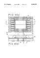
- FIGS. 1(a) and 1(b)are respectively views for describing a first embodiment of the present invention.
- FIG. 1(a)is a plan view and
- FIG. 1(b)is a cross-sectional view taken along line A-A' of FIG. 1(a).
- a base material 1 composed of a glass epoxy materialis first prepared.
- the base material 1has external terminals 2 formed on the back thereof, which are electrically connected to the outside, and conductor or conductive patterns 3 formed on the surface thereof.
- the external terminals 2 and the conductive patterns 3are respectively electrically connected to one another by vias 4.
- a solder resist 6is applied onto the base material 1 as a resist layer composed of an insulating resin. Now, the solder resist 6 is applied onto portions of electrodes 5 electrically connected to a semiconductor element or elemental device, which are for the conductive patterns 3 and portions thereof on which the semiconductor elemental device 8 is mounted in a state in which the periphery of the base material 1 is bare.
- the solder resist 6is applied onto substantially the same area as that for the semiconductor elemental device 8 as an area to be applied.
- the solder resist 6is applied to the above portions by using, as the applying methods, methods known per se in the art, such as a printing method for applying a resist through, for example, a mask placed on a base material, an exposure system for applying a resist over the entire surface of a base material and thereafter removing unnecessary portions by exposure and development.
- the semiconductor elemental device 8is fixed onto the applied solder resist 6 by an adhesive 7.
- Silver paste, an epoxy material or the likemay preferably be used as the adhesive.
- an adhesive tapemay be used as the adhesive.
- Electrodes 9 on the semiconductor elemental device 8 and the electrodes 5 of the conductive patternsare respectively electrically connected to one another by metal thin lines 10 by using the known wire bonding.
- the base material 1 including the semiconductor elemental device 8 and the metal thin lines 10is sealed with a resin 11. This sealing is carried out by the known potting or transfer mold.
- the sealing resinis in direct contact with the base material 1 at exposed or bare potions 12 of the base material 1 at this time, the resin is high in adhesion strength as compared with the case in which the solder resist 6 is applied to the periphery of the base material 1 and hence the resin is hard to fall off or peel between the sealing resin 11 and the base material 1.
- Uneven spots or projections and depressionsmay be provided at the peripheral portions of the base material 1 as shown in FIG. 2.
- projections and depressionswhich are 0.1 mm or more in roughness, are formed around the base material 1 by drilling after the solder resist 6 has been formed on the conductive patterns 3.
- the area for adhesion between the base material 1 and the sealing resin 11increases and the base material and the sealing resin can be firmly bonded to each other, so that the resin is hard to further peel.
- FIG. 3(a)is a plan view of the second embodiment and FIG. 3(b) is a cross-sectional view taken along line A-A' of FIG. 3(a).
- the same elements of structureare identified by the same reference numerals and their description will be omitted.
- the adhesive employed in the first embodimentis not formed over the entire back of a semiconductor elemental device 8 but partly formed over the back thereof.
- the partly formed adhesives 13are formed to a predetermined height of about 30 ⁇ m with a diameter of about 0.5 mm and at intervals ranging from 1.5 mm to 2 mm with respect to each other so that the resin 11 is introduced round even into the back of the semiconductor elemental device 8 lying between the adhesives 13.
- the adhesives 13can be partly provided by discharging it through nozzles each having a predetermined size.
- sheet-like adhesives fixed in sheet formmay be used in place of the adhesives. Since the respective sheet-like adhesives become constant in thickness when the sheet-like adhesives are used, the inclination of the semiconductor elemental device 8 can be eliminated, so that a variation in the direction of the thickness of the semiconductor elemental device 8 can be reduced.
- FIG. 4(a)is a plan view and FIG. 4(b) is a cross-sectional view taken along line A-A' of FIG. 4(a).
- a base material 1 similar to that employed in the first embodimentis prepared.
- solder resistis applied onto the base material 1 as a resist layer composed of an insulating resin.
- the solder resist 15is applied to the surface of the base material 1 by a method similar to the first embodiment in a state in which portions of electrodes 5 electrically connected to a semiconductor element or elemental device, of conductive patterns 3 have been exposed.
- each solder resist 15is etched or drilled to thereby define uneven spots or projections and depressions in the surface thereof.
- the roughness of the projections and depressionsmay preferably be 0.1 mm or more.
- the semiconductor elemental device 8is fixed onto the corresponding solder resist 15 in a manner similar to the first embodiment. Electrodes on the semiconductor elemental device 8 and the electrodes 5 of the conductive patterns 3 are respectively electrically connected to one another by metal thin lines 10 using the known wire bonding. Further, the base material 1 including the semiconductor elemental device 8 and the metal thin lines 10 are sealed with a resin.
- the sealing resinis formed in areas including the projections and depressions formed in the surface of each solder resist at this time, the area for adhesion between the sealing resin and a sealing body 11 increases and hence the resin is hard to peel.
- the sealing resincontains particles called "fillers" and the diameter of each particle generally ranges from 0.5 mm to 0.75 mm. therefore, when the roughness of the projections and depressions is set to 0.1 mm or more greater than the particle diameter, the fillers enter into the projections and depressions formed in the solder resist and hence bond strength is further improved.
- FIG. 5(a)is a plan view
- FIG. 5(b)is a cross-sectional view taken along line A-A' of FIG. 5(a).
- the same elements of structureare identified by the same reference numerals and their description will be omitted.
- ends of a base material 1are rendered bare to form a solder resist 17.
- the area for adhesion between the sealing body 11 and the base material 1becomes wide so that peeling is hard to occur.
- the counter sinksmay be circular as shown in FIGS. 6(a) and 6(b).
- the counter sinksmay be via holes 19 each having such a configuration as to extend through the back of the base material 1.
- the diameter thereofmay preferably be about 0.3 mm.
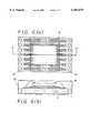
- FIG. 7(a)is a plan view
- FIG. 7(b)is a cross-sectional view taken along line A-A' of FIG. 7(a)
- FIG. 7(c)is a view showing one of semiconductor devices divided into pieces. The same elements of structure are identified by the same reference numerals and their description will be omitted.
- IC chips 8.are mounted on a base material 1 at predetermined intervals. At this time, conductive patterns 3 and a solder resist 6 are formed below each semiconductor elemental device B. Next, counter sinks 20 each having a depth of 0.1 mm or more are formed between the semiconductor elemental devices 8 of the base material 1. After the formation of the counter sinks 20, the entire surface of the base material 1 containing the semiconductor elemental devices 8 is sealed with a sealing body 11 composed of a resin. Thereafter, portions at which the counter sinks 20 are formed, are cut to obtain each individual semiconductor devices.
- FIG. 8(a)is a plan view and FIG. 8(b) is a cross-sectional view taken along line A-A' of FIG. 8(a).
- the sixth embodimentis constructed in such a manner that solder resists 21 are formed only over their corresponding conductive patterns 3 formed on a base material 1.
- the conductive patterns 3are respectively covered with the solder resists 21 except for portions 5 electrically connected to a semiconductor elemental device, a malfunction such as a short between the patterns due to foreign substances or the like is not produced either.
Landscapes
- Engineering & Computer Science (AREA)
- Microelectronics & Electronic Packaging (AREA)
- Computer Hardware Design (AREA)
- Power Engineering (AREA)
- Physics & Mathematics (AREA)
- Condensed Matter Physics & Semiconductors (AREA)
- General Physics & Mathematics (AREA)
- Structures Or Materials For Encapsulating Or Coating Semiconductor Devices Or Solid State Devices (AREA)
Abstract
Description
Claims (16)
Applications Claiming Priority (2)
| Application Number | Priority Date | Filing Date | Title |
|---|---|---|---|
| JP35282997AJP3638771B2 (en) | 1997-12-22 | 1997-12-22 | Semiconductor device |
| JP9-352829 | 1997-12-22 |
Publications (1)
| Publication Number | Publication Date |
|---|---|
| US6107679Atrue US6107679A (en) | 2000-08-22 |
Family
ID=18426729
Family Applications (1)
| Application Number | Title | Priority Date | Filing Date |
|---|---|---|---|
| US09/200,964Expired - LifetimeUS6107679A (en) | 1997-12-22 | 1998-11-30 | Semiconductor device |
Country Status (3)
| Country | Link |
|---|---|
| US (1) | US6107679A (en) |
| JP (1) | JP3638771B2 (en) |
| KR (1) | KR100522620B1 (en) |
Cited By (86)
| Publication number | Priority date | Publication date | Assignee | Title |
|---|---|---|---|---|
| US6288905B1 (en)* | 1999-04-15 | 2001-09-11 | Amerasia International Technology Inc. | Contact module, as for a smart card, and method for making same |
| US6335565B1 (en)* | 1996-12-04 | 2002-01-01 | Hitachi, Ltd. | Semiconductor device |
| US6359334B1 (en)* | 1999-06-08 | 2002-03-19 | Micron Technology, Inc. | Thermally conductive adhesive tape for semiconductor devices and method using the same |
| US6404061B1 (en)* | 1999-02-26 | 2002-06-11 | Rohm Co., Ltd. | Semiconductor device and semiconductor chip |
| US6492719B2 (en) | 1999-07-30 | 2002-12-10 | Hitachi, Ltd. | Semiconductor device |
| US6501175B2 (en)* | 2000-06-12 | 2002-12-31 | Nec Corporation | Semiconductor device with semiconductor chip on flexible tape |
| US20030116349A1 (en)* | 2000-09-05 | 2003-06-26 | Seiko Epson Corporation | Semiconductor device and method of manufacture thereof, circuit board, and electronic instrument |
| US6586277B2 (en) | 1999-07-30 | 2003-07-01 | Micron Technology, Inc. | Method and structure for manufacturing improved yield semiconductor packaged devices |
| US20030141596A1 (en)* | 2000-02-28 | 2003-07-31 | Hidehiro Nakamura | Wiring board, semiconductor device, and method of manufacturing wiring board |
| WO2003107417A1 (en)* | 2002-06-17 | 2003-12-24 | Infineon Technologies Ag | Packaging for semiconductor components and method for producing the same |
| US6731013B2 (en)* | 2000-06-28 | 2004-05-04 | Sharp Kabushiki Kaisha | Wiring substrate, semiconductor device and package stack semiconductor device |
| US20040104043A1 (en)* | 2002-09-27 | 2004-06-03 | Noriyasu Sakai | Circuit device and method of manufacturing the same |
| US20040232566A1 (en)* | 2003-05-07 | 2004-11-25 | Kiyoshi Mita | Semiconductor device and method of manufacturing the same |
| US20040245628A1 (en)* | 2003-01-14 | 2004-12-09 | Samsung Electronics Co., Ltd. | Tape package having test pad on reverse surface and method for testing the same |
| US20050011672A1 (en)* | 2003-07-17 | 2005-01-20 | Alawani Ashish D. | Overmolded MCM with increased surface mount component reliability |
| US20050046023A1 (en)* | 2003-08-28 | 2005-03-03 | Renesas Technology Corp. | Semiconductor device |
| US20050067712A1 (en)* | 2003-09-29 | 2005-03-31 | Toshikazu Imaoka | Semiconductor apparatus and method of fabricating the same |
| US6903270B1 (en)* | 2000-08-11 | 2005-06-07 | Skyworks Solutions, Inc. | Method and structure for securing a mold compound to a printed circuit board |
| US20060040428A1 (en)* | 2004-08-19 | 2006-02-23 | Johnson Mark S | Conductive structures for microfeature devices and methods for fabricating microfeature devices |
| US20060057694A1 (en)* | 2003-01-29 | 2006-03-16 | Thomas Kenneth A Jr | Rat receptor tyrosine knase, kdr |
| US20070201247A1 (en)* | 2006-02-28 | 2007-08-30 | Minebea Co., Ltd. | Spread illuminating apparatus |
| US7413979B2 (en) | 2003-11-13 | 2008-08-19 | Micron Technology, Inc. | Methods for forming vias in microelectronic devices, and methods for packaging microelectronic devices |
| US20080217751A1 (en)* | 2007-03-08 | 2008-09-11 | Matsushita Electric Industrial Co., Ltd. | Substrate for mounting semiconductor element and method of manufacturing the same |
| US7425499B2 (en) | 2004-08-24 | 2008-09-16 | Micron Technology, Inc. | Methods for forming interconnects in vias and microelectronic workpieces including such interconnects |
| US7435913B2 (en) | 2004-08-27 | 2008-10-14 | Micron Technology, Inc. | Slanted vias for electrical circuits on circuit boards and other substrates |
| US7531453B2 (en) | 2004-06-29 | 2009-05-12 | Micron Technology, Inc. | Microelectronic devices and methods for forming interconnects in microelectronic devices |
| US7560804B1 (en) | 1998-06-24 | 2009-07-14 | Amkor Technology, Inc. | Integrated circuit package and method of making the same |
| US7589008B2 (en) | 2004-12-30 | 2009-09-15 | Micron Technology, Inc. | Methods for forming interconnects in microelectronic workpieces and microelectronic workpieces formed using such methods |
| US7622377B2 (en) | 2005-09-01 | 2009-11-24 | Micron Technology, Inc. | Microfeature workpiece substrates having through-substrate vias, and associated methods of formation |
| US7629249B2 (en) | 2006-08-28 | 2009-12-08 | Micron Technology, Inc. | Microfeature workpieces having conductive interconnect structures formed by chemically reactive processes, and associated systems and methods |
| US7683458B2 (en) | 2004-09-02 | 2010-03-23 | Micron Technology, Inc. | Through-wafer interconnects for photoimager and memory wafers |
| DE102008057174A1 (en)* | 2008-11-13 | 2010-05-20 | Osram Opto Semiconductors Gmbh | Surface mountable device |
| US7723852B1 (en) | 2008-01-21 | 2010-05-25 | Amkor Technology, Inc. | Stacked semiconductor package and method of making same |
| US7732899B1 (en) | 2005-12-02 | 2010-06-08 | Amkor Technology, Inc. | Etch singulated semiconductor package |
| US7749899B2 (en) | 2006-06-01 | 2010-07-06 | Micron Technology, Inc. | Microelectronic workpieces and methods and systems for forming interconnects in microelectronic workpieces |
| US20100176501A1 (en)* | 2008-11-12 | 2010-07-15 | White Electronic Designs Corporation | Method and Apparatus for Stacked Die Package with Insulated Wire Bonds |
| US7768135B1 (en) | 2008-04-17 | 2010-08-03 | Amkor Technology, Inc. | Semiconductor package with fast power-up cycle and method of making same |
| US7795134B2 (en) | 2005-06-28 | 2010-09-14 | Micron Technology, Inc. | Conductive interconnect structures and formation methods using supercritical fluids |
| US7808084B1 (en) | 2008-05-06 | 2010-10-05 | Amkor Technology, Inc. | Semiconductor package with half-etched locking features |
| US7830018B2 (en) | 2007-08-31 | 2010-11-09 | Micron Technology, Inc. | Partitioned through-layer via and associated systems and methods |
| US7847392B1 (en) | 2008-09-30 | 2010-12-07 | Amkor Technology, Inc. | Semiconductor device including leadframe with increased I/O |
| US7863187B2 (en) | 2005-09-01 | 2011-01-04 | Micron Technology, Inc. | Microfeature workpieces and methods for forming interconnects in microfeature workpieces |
| US7875963B1 (en) | 2008-11-21 | 2011-01-25 | Amkor Technology, Inc. | Semiconductor device including leadframe having power bars and increased I/O |
| US7884015B2 (en) | 2007-12-06 | 2011-02-08 | Micron Technology, Inc. | Methods for forming interconnects in microelectronic workpieces and microelectronic workpieces formed using such methods |
| US7902643B2 (en) | 2006-08-31 | 2011-03-08 | Micron Technology, Inc. | Microfeature workpieces having interconnects and conductive backplanes, and associated systems and methods |
| US7915736B2 (en) | 2005-09-01 | 2011-03-29 | Micron Technology, Inc. | Microfeature workpieces and methods for forming interconnects in microfeature workpieces |
| US7928542B2 (en) | 2001-03-27 | 2011-04-19 | Amkor Technology, Inc. | Lead frame for semiconductor package |
| US7956453B1 (en) | 2008-01-16 | 2011-06-07 | Amkor Technology, Inc. | Semiconductor package with patterning layer and method of making same |
| US7960818B1 (en) | 2009-03-04 | 2011-06-14 | Amkor Technology, Inc. | Conformal shield on punch QFN semiconductor package |
| US7982298B1 (en) | 2008-12-03 | 2011-07-19 | Amkor Technology, Inc. | Package in package semiconductor device |
| US20110181488A1 (en)* | 2010-01-25 | 2011-07-28 | Freescale Semiconductor, Inc. | Electronic device module with integrated antenna structure, and related manufacturing method |
| US7989933B1 (en) | 2008-10-06 | 2011-08-02 | Amkor Technology, Inc. | Increased I/O leadframe and semiconductor device including same |
| US8008758B1 (en) | 2008-10-27 | 2011-08-30 | Amkor Technology, Inc. | Semiconductor device with increased I/O leadframe |
| US8026589B1 (en) | 2009-02-23 | 2011-09-27 | Amkor Technology, Inc. | Reduced profile stackable semiconductor package |
| US8058715B1 (en) | 2009-01-09 | 2011-11-15 | Amkor Technology, Inc. | Package in package device for RF transceiver module |
| US8067821B1 (en) | 2008-04-10 | 2011-11-29 | Amkor Technology, Inc. | Flat semiconductor package with half package molding |
| US8072050B1 (en) | 2008-11-18 | 2011-12-06 | Amkor Technology, Inc. | Semiconductor device with increased I/O leadframe including passive device |
| US8084866B2 (en) | 2003-12-10 | 2011-12-27 | Micron Technology, Inc. | Microelectronic devices and methods for filling vias in microelectronic devices |
| US8089145B1 (en) | 2008-11-17 | 2012-01-03 | Amkor Technology, Inc. | Semiconductor device including increased capacity leadframe |
| US8125064B1 (en) | 2008-07-28 | 2012-02-28 | Amkor Technology, Inc. | Increased I/O semiconductor package and method of making same |
| US8184453B1 (en) | 2008-07-31 | 2012-05-22 | Amkor Technology, Inc. | Increased capacity semiconductor package |
| US20120133056A1 (en)* | 2006-04-20 | 2012-05-31 | Shinko Electric Industries Co., Ltd. | Semiconductor device, electronic apparatus and semiconductor device fabricating method |
| US8304866B1 (en) | 2007-07-10 | 2012-11-06 | Amkor Technology, Inc. | Fusion quad flat semiconductor package |
| US8318287B1 (en) | 1998-06-24 | 2012-11-27 | Amkor Technology, Inc. | Integrated circuit package and method of making the same |
| US8441110B1 (en) | 2006-06-21 | 2013-05-14 | Amkor Technology, Inc. | Side leaded, bottom exposed pad and bottom exposed lead fusion quad flat semiconductor package |
| US8487420B1 (en) | 2008-12-08 | 2013-07-16 | Amkor Technology, Inc. | Package in package semiconductor device with film over wire |
| US8536485B2 (en) | 2004-05-05 | 2013-09-17 | Micron Technology, Inc. | Systems and methods for forming apertures in microfeature workpieces |
| US8575742B1 (en) | 2009-04-06 | 2013-11-05 | Amkor Technology, Inc. | Semiconductor device with increased I/O leadframe including power bars |
| US20140001634A1 (en)* | 2012-06-27 | 2014-01-02 | Infineon Technologies Ag | Chip package and methods for manufacturing a chip package |
| US8648450B1 (en) | 2011-01-27 | 2014-02-11 | Amkor Technology, Inc. | Semiconductor device including leadframe with a combination of leads and lands |
| US8680656B1 (en) | 2009-01-05 | 2014-03-25 | Amkor Technology, Inc. | Leadframe structure for concentrated photovoltaic receiver package |
| US20140091459A1 (en)* | 2008-05-09 | 2014-04-03 | Invensas Corporation | Chip-size, double side connection package and method for manufacturing the same |
| US9184118B2 (en) | 2013-05-02 | 2015-11-10 | Amkor Technology Inc. | Micro lead frame structure having reinforcing portions and method |
| US9184148B2 (en) | 2013-10-24 | 2015-11-10 | Amkor Technology, Inc. | Semiconductor package and method therefor |
| USRE45931E1 (en) | 1999-11-29 | 2016-03-15 | Renesas Electronics Corporation | Method of manufacturing a semiconductor device |
| US9631481B1 (en) | 2011-01-27 | 2017-04-25 | Amkor Technology, Inc. | Semiconductor device including leadframe with a combination of leads and lands and method |
| US9673122B2 (en) | 2014-05-02 | 2017-06-06 | Amkor Technology, Inc. | Micro lead frame structure having reinforcing portions and method |
| US9704725B1 (en) | 2012-03-06 | 2017-07-11 | Amkor Technology, Inc. | Semiconductor device with leadframe configured to facilitate reduced burr formation |
| CN108614371A (en)* | 2018-04-03 | 2018-10-02 | 惠州市华星光电技术有限公司 | Display device and its manufacturing method |
| US10181447B2 (en) | 2017-04-21 | 2019-01-15 | Invensas Corporation | 3D-interconnect |
| US20190348387A1 (en)* | 2013-03-14 | 2019-11-14 | UTAC Headquarters Pte. Ltd. | Semiconductor packages and methods of packaging semiconductor devices |
| US10522610B2 (en)* | 2018-04-03 | 2019-12-31 | Huizhou China Star Optoelectronics Technology Co., Ltd. | Display device with hemispherical particles on chip-on-film surface, and manufacturing method thereof |
| US10811341B2 (en) | 2009-01-05 | 2020-10-20 | Amkor Technology Singapore Holding Pte Ltd. | Semiconductor device with through-mold via |
| FR3111471A1 (en)* | 2020-06-15 | 2021-12-17 | Stmicroelectronics (Grenoble 2) Sas | Support substrate for integrated circuit, electronic device, and corresponding production and packaging methods. |
| US11894325B2 (en) | 2018-11-15 | 2024-02-06 | Rohm Co., Ltd. | Semiconductor device having a resin that seals a rewiring |
| US12040284B2 (en) | 2021-11-12 | 2024-07-16 | Invensas Llc | 3D-interconnect with electromagnetic interference (“EMI”) shield and/or antenna |
Families Citing this family (3)
| Publication number | Priority date | Publication date | Assignee | Title |
|---|---|---|---|---|
| JP4593831B2 (en)* | 2001-06-04 | 2010-12-08 | 新日本無線株式会社 | Chip size package |
| JP4614818B2 (en)* | 2005-05-09 | 2011-01-19 | パナソニック株式会社 | Semiconductor device and manufacturing method thereof |
| JP2012073233A (en)* | 2010-08-31 | 2012-04-12 | Mitsumi Electric Co Ltd | Sensor device and mounting method of semiconductor sensor element |
Citations (21)
| Publication number | Priority date | Publication date | Assignee | Title |
|---|---|---|---|---|
| US5285352A (en)* | 1992-07-15 | 1994-02-08 | Motorola, Inc. | Pad array semiconductor device with thermal conductor and process for making the same |
| US5334857A (en)* | 1992-04-06 | 1994-08-02 | Motorola, Inc. | Semiconductor device with test-only contacts and method for making the same |
| US5399903A (en)* | 1990-08-15 | 1995-03-21 | Lsi Logic Corporation | Semiconductor device having an universal die size inner lead layout |
| US5455456A (en)* | 1993-09-15 | 1995-10-03 | Lsi Logic Corporation | Integrated circuit package lid |
| US5521435A (en)* | 1993-12-13 | 1996-05-28 | Fujitsu Limited | Semiconductor device and a fabrication process thereof |
| US5581122A (en)* | 1994-10-25 | 1996-12-03 | Industrial Technology Research Institute | Packaging assembly with consolidated common voltage connections for integrated circuits |
| US5592025A (en)* | 1992-08-06 | 1997-01-07 | Motorola, Inc. | Pad array semiconductor device |
| US5612576A (en)* | 1992-10-13 | 1997-03-18 | Motorola | Self-opening vent hole in an overmolded semiconductor device |
| US5640042A (en)* | 1995-12-14 | 1997-06-17 | The United States Of America As Represented By The Secretary Of The Army | Thin film ferroelectric varactor |
| US5657550A (en)* | 1994-10-12 | 1997-08-19 | Js Research And Development, Inc. | Hand-held gap and contour measuring gauge |
| US5736780A (en)* | 1995-11-07 | 1998-04-07 | Shinko Electric Industries Co., Ltd. | Semiconductor device having circuit pattern along outer periphery of sealing resin and related processes |
| US5739588A (en)* | 1994-08-15 | 1998-04-14 | Citizen Watch Co., Ltd. | Semiconductor device |
| US5773895A (en)* | 1996-04-03 | 1998-06-30 | Intel Corporation | Anchor provisions to prevent mold delamination in an overmolded plastic array package |
| US5777381A (en)* | 1996-04-15 | 1998-07-07 | Nissin Co., Ltd. | Semiconductor devices method of connecting semiconductor devices and semiconductor device connectors |
| US5814883A (en)* | 1995-10-04 | 1998-09-29 | Mitsubishi Denki Kabushiki Kaisha | Packaged semiconductor chip |
| US5821608A (en)* | 1995-09-08 | 1998-10-13 | Tessera, Inc. | Laterally situated stress/strain relieving lead for a semiconductor chip package |
| US5859475A (en)* | 1996-04-24 | 1999-01-12 | Amkor Technology, Inc. | Carrier strip and molded flex circuit ball grid array |
| US5866942A (en)* | 1995-04-28 | 1999-02-02 | Nec Corporation | Metal base package for a semiconductor device |
| US5879568A (en)* | 1996-06-18 | 1999-03-09 | Hitachi, Ltd. | Process for producing multilayer printed circuit board for wire bonding |
| US5893508A (en)* | 1995-12-30 | 1999-04-13 | Samsung Electronics Co., Ltd. | Circuit board having a terminal for detecting disconnection of a bonding wire and a wire bonding apparatus using such a board |
| US5918113A (en)* | 1996-07-19 | 1999-06-29 | Shinko Electric Industries Co., Ltd. | Process for producing a semiconductor device using anisotropic conductive adhesive |
Family Cites Families (3)
| Publication number | Priority date | Publication date | Assignee | Title |
|---|---|---|---|---|
| JPH03257951A (en)* | 1990-03-08 | 1991-11-18 | Fujitsu Ltd | Bare chip sealing structure |
| JPH0497550A (en)* | 1990-08-14 | 1992-03-30 | Matsushita Electric Works Ltd | Sealing structure of semiconductor chip |
| JPH0685132A (en)* | 1992-09-07 | 1994-03-25 | Mitsubishi Electric Corp | Semiconductor device |
- 1997
- 1997-12-22JPJP35282997Apatent/JP3638771B2/ennot_activeExpired - Lifetime
- 1998
- 1998-11-30USUS09/200,964patent/US6107679A/ennot_activeExpired - Lifetime
- 1998-12-16KRKR1019980055389Apatent/KR100522620B1/ennot_activeExpired - Lifetime
Patent Citations (21)
| Publication number | Priority date | Publication date | Assignee | Title |
|---|---|---|---|---|
| US5399903A (en)* | 1990-08-15 | 1995-03-21 | Lsi Logic Corporation | Semiconductor device having an universal die size inner lead layout |
| US5334857A (en)* | 1992-04-06 | 1994-08-02 | Motorola, Inc. | Semiconductor device with test-only contacts and method for making the same |
| US5285352A (en)* | 1992-07-15 | 1994-02-08 | Motorola, Inc. | Pad array semiconductor device with thermal conductor and process for making the same |
| US5592025A (en)* | 1992-08-06 | 1997-01-07 | Motorola, Inc. | Pad array semiconductor device |
| US5612576A (en)* | 1992-10-13 | 1997-03-18 | Motorola | Self-opening vent hole in an overmolded semiconductor device |
| US5455456A (en)* | 1993-09-15 | 1995-10-03 | Lsi Logic Corporation | Integrated circuit package lid |
| US5521435A (en)* | 1993-12-13 | 1996-05-28 | Fujitsu Limited | Semiconductor device and a fabrication process thereof |
| US5739588A (en)* | 1994-08-15 | 1998-04-14 | Citizen Watch Co., Ltd. | Semiconductor device |
| US5657550A (en)* | 1994-10-12 | 1997-08-19 | Js Research And Development, Inc. | Hand-held gap and contour measuring gauge |
| US5581122A (en)* | 1994-10-25 | 1996-12-03 | Industrial Technology Research Institute | Packaging assembly with consolidated common voltage connections for integrated circuits |
| US5866942A (en)* | 1995-04-28 | 1999-02-02 | Nec Corporation | Metal base package for a semiconductor device |
| US5821608A (en)* | 1995-09-08 | 1998-10-13 | Tessera, Inc. | Laterally situated stress/strain relieving lead for a semiconductor chip package |
| US5814883A (en)* | 1995-10-04 | 1998-09-29 | Mitsubishi Denki Kabushiki Kaisha | Packaged semiconductor chip |
| US5736780A (en)* | 1995-11-07 | 1998-04-07 | Shinko Electric Industries Co., Ltd. | Semiconductor device having circuit pattern along outer periphery of sealing resin and related processes |
| US5640042A (en)* | 1995-12-14 | 1997-06-17 | The United States Of America As Represented By The Secretary Of The Army | Thin film ferroelectric varactor |
| US5893508A (en)* | 1995-12-30 | 1999-04-13 | Samsung Electronics Co., Ltd. | Circuit board having a terminal for detecting disconnection of a bonding wire and a wire bonding apparatus using such a board |
| US5773895A (en)* | 1996-04-03 | 1998-06-30 | Intel Corporation | Anchor provisions to prevent mold delamination in an overmolded plastic array package |
| US5777381A (en)* | 1996-04-15 | 1998-07-07 | Nissin Co., Ltd. | Semiconductor devices method of connecting semiconductor devices and semiconductor device connectors |
| US5859475A (en)* | 1996-04-24 | 1999-01-12 | Amkor Technology, Inc. | Carrier strip and molded flex circuit ball grid array |
| US5879568A (en)* | 1996-06-18 | 1999-03-09 | Hitachi, Ltd. | Process for producing multilayer printed circuit board for wire bonding |
| US5918113A (en)* | 1996-07-19 | 1999-06-29 | Shinko Electric Industries Co., Ltd. | Process for producing a semiconductor device using anisotropic conductive adhesive |
Cited By (172)
| Publication number | Priority date | Publication date | Assignee | Title |
|---|---|---|---|---|
| US6611012B2 (en) | 1996-12-04 | 2003-08-26 | Hitachi, Ltd. | Semiconductor device |
| US6335565B1 (en)* | 1996-12-04 | 2002-01-01 | Hitachi, Ltd. | Semiconductor device |
| US20050146008A1 (en)* | 1996-12-04 | 2005-07-07 | Renesas Technology Corp. | Semiconductor device |
| US7138722B2 (en) | 1996-12-04 | 2006-11-21 | Renesas Technology Corp. | Semiconductor device |
| US8318287B1 (en) | 1998-06-24 | 2012-11-27 | Amkor Technology, Inc. | Integrated circuit package and method of making the same |
| US7560804B1 (en) | 1998-06-24 | 2009-07-14 | Amkor Technology, Inc. | Integrated circuit package and method of making the same |
| US9224676B1 (en) | 1998-06-24 | 2015-12-29 | Amkor Technology, Inc. | Integrated circuit package and method of making the same |
| US8963301B1 (en) | 1998-06-24 | 2015-02-24 | Amkor Technology, Inc. | Integrated circuit package and method of making the same |
| US8853836B1 (en) | 1998-06-24 | 2014-10-07 | Amkor Technology, Inc. | Integrated circuit package and method of making the same |
| US6404061B1 (en)* | 1999-02-26 | 2002-06-11 | Rohm Co., Ltd. | Semiconductor device and semiconductor chip |
| US6288905B1 (en)* | 1999-04-15 | 2001-09-11 | Amerasia International Technology Inc. | Contact module, as for a smart card, and method for making same |
| US6737299B1 (en) | 1999-06-08 | 2004-05-18 | Micron Technology, Inc. | Thermally conductive adhesive tape for semiconductor devices and method for using the same |
| US6359334B1 (en)* | 1999-06-08 | 2002-03-19 | Micron Technology, Inc. | Thermally conductive adhesive tape for semiconductor devices and method using the same |
| US6630731B2 (en) | 1999-07-30 | 2003-10-07 | Hitachi, Ltd. | Semiconductor device |
| US20030209740A1 (en)* | 1999-07-30 | 2003-11-13 | Hitachi, Ltd. | Semiconductor device |
| US6774480B1 (en) | 1999-07-30 | 2004-08-10 | Micron Technology, Inc. | Method and structure for manufacturing improved yield semiconductor packaged devices |
| US6492719B2 (en) | 1999-07-30 | 2002-12-10 | Hitachi, Ltd. | Semiconductor device |
| US6900074B2 (en) | 1999-07-30 | 2005-05-31 | Renesas Technology Corp. | Method of manufacturing a semiconductor device having plural semiconductor chips, wherein electrodes of the semiconductor chips are electrically connected together via wiring substrates of the semiconductor chips |
| US6902956B2 (en) | 1999-07-30 | 2005-06-07 | Micron Technology, Inc. | Method and structure for manufacturing improved yield semiconductor packaged devices |
| US6586277B2 (en) | 1999-07-30 | 2003-07-01 | Micron Technology, Inc. | Method and structure for manufacturing improved yield semiconductor packaged devices |
| USRE45931E1 (en) | 1999-11-29 | 2016-03-15 | Renesas Electronics Corporation | Method of manufacturing a semiconductor device |
| US7704799B2 (en) | 2000-02-28 | 2010-04-27 | Hitachi Chemical Co., Ltd. | Method of manufacturing wiring substrate |
| US20030141596A1 (en)* | 2000-02-28 | 2003-07-31 | Hidehiro Nakamura | Wiring board, semiconductor device, and method of manufacturing wiring board |
| US20070161228A1 (en)* | 2000-02-28 | 2007-07-12 | Hitachi Chemical Co., Ltd. | Wiring substrate and semiconductor device, and method of manufacturing wiring substrate |
| US7205645B2 (en)* | 2000-02-28 | 2007-04-17 | Hitachi Chemical Co., Ltd. | Wiring board, semiconductor device, and method of manufacturing wiring board |
| US6501175B2 (en)* | 2000-06-12 | 2002-12-31 | Nec Corporation | Semiconductor device with semiconductor chip on flexible tape |
| US6731013B2 (en)* | 2000-06-28 | 2004-05-04 | Sharp Kabushiki Kaisha | Wiring substrate, semiconductor device and package stack semiconductor device |
| US6903270B1 (en)* | 2000-08-11 | 2005-06-07 | Skyworks Solutions, Inc. | Method and structure for securing a mold compound to a printed circuit board |
| US20030116349A1 (en)* | 2000-09-05 | 2003-06-26 | Seiko Epson Corporation | Semiconductor device and method of manufacture thereof, circuit board, and electronic instrument |
| US20060090931A1 (en)* | 2000-09-05 | 2006-05-04 | Seiko Epson Corporation | Semiconductor device and method for manufacture thereof, circuit board, and electronic Instrument |
| US7067741B2 (en)* | 2000-09-05 | 2006-06-27 | Seiko Epson Corporation | Semiconductor device and method of manufacture thereof, circuit board, and electronic instrument |
| US7129420B2 (en) | 2000-09-05 | 2006-10-31 | Seiko Epson Corporation | Semiconductor device and method for manufacture thereof, circuit board, and electronic instrument |
| US7928542B2 (en) | 2001-03-27 | 2011-04-19 | Amkor Technology, Inc. | Lead frame for semiconductor package |
| US8102037B2 (en) | 2001-03-27 | 2012-01-24 | Amkor Technology, Inc. | Leadframe for semiconductor package |
| US7384822B2 (en) | 2002-06-17 | 2008-06-10 | Infineon Technologies Ag | Package for semiconductor components and method for producing the same |
| WO2003107417A1 (en)* | 2002-06-17 | 2003-12-24 | Infineon Technologies Ag | Packaging for semiconductor components and method for producing the same |
| US20040104043A1 (en)* | 2002-09-27 | 2004-06-03 | Noriyasu Sakai | Circuit device and method of manufacturing the same |
| US7217990B2 (en)* | 2003-01-14 | 2007-05-15 | Samsung Electronics Co., Ltd. | Tape package having test pad on reverse surface and method for testing the same |
| US20040245628A1 (en)* | 2003-01-14 | 2004-12-09 | Samsung Electronics Co., Ltd. | Tape package having test pad on reverse surface and method for testing the same |
| US20060057694A1 (en)* | 2003-01-29 | 2006-03-16 | Thomas Kenneth A Jr | Rat receptor tyrosine knase, kdr |
| US20040232566A1 (en)* | 2003-05-07 | 2004-11-25 | Kiyoshi Mita | Semiconductor device and method of manufacturing the same |
| US20050011672A1 (en)* | 2003-07-17 | 2005-01-20 | Alawani Ashish D. | Overmolded MCM with increased surface mount component reliability |
| US7479705B2 (en)* | 2003-08-28 | 2009-01-20 | Renesas Technology Corp. | Semiconductor device |
| US20090091031A1 (en)* | 2003-08-28 | 2009-04-09 | Noriyuki Takahashi | Semiconductor device |
| US20050046023A1 (en)* | 2003-08-28 | 2005-03-03 | Renesas Technology Corp. | Semiconductor device |
| US7615872B2 (en) | 2003-08-28 | 2009-11-10 | Renesas Technology Corp. | Semiconductor device |
| US20050067712A1 (en)* | 2003-09-29 | 2005-03-31 | Toshikazu Imaoka | Semiconductor apparatus and method of fabricating the same |
| US7413979B2 (en) | 2003-11-13 | 2008-08-19 | Micron Technology, Inc. | Methods for forming vias in microelectronic devices, and methods for packaging microelectronic devices |
| US9653420B2 (en) | 2003-11-13 | 2017-05-16 | Micron Technology, Inc. | Microelectronic devices and methods for filling vias in microelectronic devices |
| US7759800B2 (en) | 2003-11-13 | 2010-07-20 | Micron Technology, Inc. | Microelectronics devices, having vias, and packaged microelectronic devices having vias |
| US8748311B2 (en) | 2003-12-10 | 2014-06-10 | Micron Technology, Inc. | Microelectronic devices and methods for filing vias in microelectronic devices |
| US11177175B2 (en) | 2003-12-10 | 2021-11-16 | Micron Technology, Inc. | Microelectronic devices and methods for filling vias in microelectronic devices |
| US8084866B2 (en) | 2003-12-10 | 2011-12-27 | Micron Technology, Inc. | Microelectronic devices and methods for filling vias in microelectronic devices |
| US9452492B2 (en) | 2004-05-05 | 2016-09-27 | Micron Technology, Inc. | Systems and methods for forming apertures in microfeature workpieces |
| US8664562B2 (en) | 2004-05-05 | 2014-03-04 | Micron Technology, Inc. | Systems and methods for forming apertures in microfeature workpieces |
| US8686313B2 (en) | 2004-05-05 | 2014-04-01 | Micron Technology, Inc. | System and methods for forming apertures in microfeature workpieces |
| US10010977B2 (en) | 2004-05-05 | 2018-07-03 | Micron Technology, Inc. | Systems and methods for forming apertures in microfeature workpieces |
| US8536485B2 (en) | 2004-05-05 | 2013-09-17 | Micron Technology, Inc. | Systems and methods for forming apertures in microfeature workpieces |
| US7531453B2 (en) | 2004-06-29 | 2009-05-12 | Micron Technology, Inc. | Microelectronic devices and methods for forming interconnects in microelectronic devices |
| US20090191701A1 (en)* | 2004-06-29 | 2009-07-30 | Micron Technology, Inc. | Microelectronic devices and methods for forming interconnects in microelectronic devices |
| US7829976B2 (en) | 2004-06-29 | 2010-11-09 | Micron Technology, Inc. | Microelectronic devices and methods for forming interconnects in microelectronic devices |
| US8222727B2 (en) | 2004-08-19 | 2012-07-17 | Micron Technology, Inc. | Conductive structures for microfeature devices and methods for fabricating microfeature devices |
| US20100044876A1 (en)* | 2004-08-19 | 2010-02-25 | Micron Technology, Inc. | Conductive structures for microfeature devices and methods for fabricating microfeature devices |
| US9313902B2 (en) | 2004-08-19 | 2016-04-12 | Micron Technology, Inc. | Conductive structures for microfeature devices and methods for fabricating microfeature devices |
| US20060040428A1 (en)* | 2004-08-19 | 2006-02-23 | Johnson Mark S | Conductive structures for microfeature devices and methods for fabricating microfeature devices |
| US7632747B2 (en)* | 2004-08-19 | 2009-12-15 | Micron Technology, Inc. | Conductive structures for microfeature devices and methods for fabricating microfeature devices |
| US7425499B2 (en) | 2004-08-24 | 2008-09-16 | Micron Technology, Inc. | Methods for forming interconnects in vias and microelectronic workpieces including such interconnects |
| US7435913B2 (en) | 2004-08-27 | 2008-10-14 | Micron Technology, Inc. | Slanted vias for electrical circuits on circuit boards and other substrates |
| US20090008144A1 (en)* | 2004-08-27 | 2009-01-08 | Micron Technology, Inc. | Slanted vias for electrical circuits on circuit boards and other substrates |
| US8322031B2 (en) | 2004-08-27 | 2012-12-04 | Micron Technology, Inc. | Method of manufacturing an interposer |
| US7683458B2 (en) | 2004-09-02 | 2010-03-23 | Micron Technology, Inc. | Through-wafer interconnects for photoimager and memory wafers |
| US8669179B2 (en) | 2004-09-02 | 2014-03-11 | Micron Technology, Inc. | Through-wafer interconnects for photoimager and memory wafers |
| US8502353B2 (en) | 2004-09-02 | 2013-08-06 | Micron Technology, Inc. | Through-wafer interconnects for photoimager and memory wafers |
| US7956443B2 (en) | 2004-09-02 | 2011-06-07 | Micron Technology, Inc. | Through-wafer interconnects for photoimager and memory wafers |
| US9214391B2 (en) | 2004-12-30 | 2015-12-15 | Micron Technology, Inc. | Methods for forming interconnects in microelectronic workpieces and microelectronic workpieces formed using such methods |
| US7589008B2 (en) | 2004-12-30 | 2009-09-15 | Micron Technology, Inc. | Methods for forming interconnects in microelectronic workpieces and microelectronic workpieces formed using such methods |
| US9293367B2 (en) | 2005-06-28 | 2016-03-22 | Micron Technology, Inc. | Conductive interconnect structures and formation methods using supercritical fluids |
| US7795134B2 (en) | 2005-06-28 | 2010-09-14 | Micron Technology, Inc. | Conductive interconnect structures and formation methods using supercritical fluids |
| US8008192B2 (en) | 2005-06-28 | 2011-08-30 | Micron Technology, Inc. | Conductive interconnect structures and formation methods using supercritical fluids |
| US7863187B2 (en) | 2005-09-01 | 2011-01-04 | Micron Technology, Inc. | Microfeature workpieces and methods for forming interconnects in microfeature workpieces |
| US7915736B2 (en) | 2005-09-01 | 2011-03-29 | Micron Technology, Inc. | Microfeature workpieces and methods for forming interconnects in microfeature workpieces |
| US11476160B2 (en) | 2005-09-01 | 2022-10-18 | Micron Technology, Inc. | Microfeature workpieces and methods for forming interconnects in microfeature workpieces |
| US12014958B2 (en) | 2005-09-01 | 2024-06-18 | Micron Technology, Inc. | Microfeature workpieces and methods for forming interconnects in microfeature workpieces |
| US7622377B2 (en) | 2005-09-01 | 2009-11-24 | Micron Technology, Inc. | Microfeature workpiece substrates having through-substrate vias, and associated methods of formation |
| US7732899B1 (en) | 2005-12-02 | 2010-06-08 | Amkor Technology, Inc. | Etch singulated semiconductor package |
| US20070201247A1 (en)* | 2006-02-28 | 2007-08-30 | Minebea Co., Ltd. | Spread illuminating apparatus |
| US7532479B2 (en)* | 2006-02-28 | 2009-05-12 | Minebea Co., Ltd. | Spread illuminating apparatus |
| US20120133056A1 (en)* | 2006-04-20 | 2012-05-31 | Shinko Electric Industries Co., Ltd. | Semiconductor device, electronic apparatus and semiconductor device fabricating method |
| US7749899B2 (en) | 2006-06-01 | 2010-07-06 | Micron Technology, Inc. | Microelectronic workpieces and methods and systems for forming interconnects in microelectronic workpieces |
| US8441110B1 (en) | 2006-06-21 | 2013-05-14 | Amkor Technology, Inc. | Side leaded, bottom exposed pad and bottom exposed lead fusion quad flat semiconductor package |
| US8610279B2 (en) | 2006-08-28 | 2013-12-17 | Micron Technologies, Inc. | Microfeature workpieces having conductive interconnect structures formed by chemically reactive processes, and associated systems and methods |
| US7629249B2 (en) | 2006-08-28 | 2009-12-08 | Micron Technology, Inc. | Microfeature workpieces having conductive interconnect structures formed by chemically reactive processes, and associated systems and methods |
| US7973411B2 (en) | 2006-08-28 | 2011-07-05 | Micron Technology, Inc. | Microfeature workpieces having conductive interconnect structures formed by chemically reactive processes, and associated systems and methods |
| US9570350B2 (en) | 2006-08-31 | 2017-02-14 | Micron Technology, Inc. | Microfeature workpieces having interconnects and conductive backplanes, and associated systems and methods |
| US7902643B2 (en) | 2006-08-31 | 2011-03-08 | Micron Technology, Inc. | Microfeature workpieces having interconnects and conductive backplanes, and associated systems and methods |
| US9099539B2 (en) | 2006-08-31 | 2015-08-04 | Micron Technology, Inc. | Microfeature workpieces having interconnects and conductive backplanes, and associated systems and methods |
| US20110151621A1 (en)* | 2006-08-31 | 2011-06-23 | Micron Technology, Inc. | Microfeature workpieces having interconnects and conductive backplanes, and associated systems and methods |
| US20080217751A1 (en)* | 2007-03-08 | 2008-09-11 | Matsushita Electric Industrial Co., Ltd. | Substrate for mounting semiconductor element and method of manufacturing the same |
| US7714417B2 (en)* | 2007-03-08 | 2010-05-11 | Panasonic Corporation | Substrate for mounting semiconductor element and method of manufacturing the same |
| US8304866B1 (en) | 2007-07-10 | 2012-11-06 | Amkor Technology, Inc. | Fusion quad flat semiconductor package |
| US20110019372A1 (en)* | 2007-08-31 | 2011-01-27 | Micron Technology, Inc. | Partitioned through-layer via and associated systems and methods |
| US8367538B2 (en) | 2007-08-31 | 2013-02-05 | Micron Technology, Inc. | Partitioned through-layer via and associated systems and methods |
| US7830018B2 (en) | 2007-08-31 | 2010-11-09 | Micron Technology, Inc. | Partitioned through-layer via and associated systems and methods |
| US8536046B2 (en) | 2007-08-31 | 2013-09-17 | Micron Technology | Partitioned through-layer via and associated systems and methods |
| US9281241B2 (en) | 2007-12-06 | 2016-03-08 | Micron Technology, Inc. | Methods for forming interconnects in microelectronic workpieces and microelectronic workpieces formed using such methods |
| US20110133302A1 (en)* | 2007-12-06 | 2011-06-09 | Micron Technology, Inc. | Methods for forming interconnects in microelectronic workpieces and microelectronic workpieces formed using such methods |
| US8247907B2 (en) | 2007-12-06 | 2012-08-21 | Micron Technology, Inc. | Methods for forming interconnects in microelectronic workpieces and microelectronic workpieces formed using such methods |
| US7884015B2 (en) | 2007-12-06 | 2011-02-08 | Micron Technology, Inc. | Methods for forming interconnects in microelectronic workpieces and microelectronic workpieces formed using such methods |
| US8729710B1 (en) | 2008-01-16 | 2014-05-20 | Amkor Technology, Inc. | Semiconductor package with patterning layer and method of making same |
| US7956453B1 (en) | 2008-01-16 | 2011-06-07 | Amkor Technology, Inc. | Semiconductor package with patterning layer and method of making same |
| US7723852B1 (en) | 2008-01-21 | 2010-05-25 | Amkor Technology, Inc. | Stacked semiconductor package and method of making same |
| US7906855B1 (en) | 2008-01-21 | 2011-03-15 | Amkor Technology, Inc. | Stacked semiconductor package and method of making same |
| US8067821B1 (en) | 2008-04-10 | 2011-11-29 | Amkor Technology, Inc. | Flat semiconductor package with half package molding |
| US8084868B1 (en) | 2008-04-17 | 2011-12-27 | Amkor Technology, Inc. | Semiconductor package with fast power-up cycle and method of making same |
| US7768135B1 (en) | 2008-04-17 | 2010-08-03 | Amkor Technology, Inc. | Semiconductor package with fast power-up cycle and method of making same |
| US7808084B1 (en) | 2008-05-06 | 2010-10-05 | Amkor Technology, Inc. | Semiconductor package with half-etched locking features |
| US10748840B2 (en)* | 2008-05-09 | 2020-08-18 | Invensas Corporation | Chip-size, double side connection package and method for manufacturing the same |
| US20180269141A1 (en)* | 2008-05-09 | 2018-09-20 | Invensas Corporation | Chip-size, double side connection package and method for manufacturing the same |
| US20140091459A1 (en)* | 2008-05-09 | 2014-04-03 | Invensas Corporation | Chip-size, double side connection package and method for manufacturing the same |
| US9984961B2 (en)* | 2008-05-09 | 2018-05-29 | Invensas Corporation | Chip-size, double side connection package and method for manufacturing the same |
| US8125064B1 (en) | 2008-07-28 | 2012-02-28 | Amkor Technology, Inc. | Increased I/O semiconductor package and method of making same |
| US8184453B1 (en) | 2008-07-31 | 2012-05-22 | Amkor Technology, Inc. | Increased capacity semiconductor package |
| US8299602B1 (en) | 2008-09-30 | 2012-10-30 | Amkor Technology, Inc. | Semiconductor device including leadframe with increased I/O |
| US7847392B1 (en) | 2008-09-30 | 2010-12-07 | Amkor Technology, Inc. | Semiconductor device including leadframe with increased I/O |
| US8432023B1 (en) | 2008-10-06 | 2013-04-30 | Amkor Technology, Inc. | Increased I/O leadframe and semiconductor device including same |
| US7989933B1 (en) | 2008-10-06 | 2011-08-02 | Amkor Technology, Inc. | Increased I/O leadframe and semiconductor device including same |
| US8823152B1 (en) | 2008-10-27 | 2014-09-02 | Amkor Technology, Inc. | Semiconductor device with increased I/O leadframe |
| US8008758B1 (en) | 2008-10-27 | 2011-08-30 | Amkor Technology, Inc. | Semiconductor device with increased I/O leadframe |
| US7939928B2 (en)* | 2008-11-12 | 2011-05-10 | Microsemi Corporation | Method and apparatus for stacked die package with insulated wire bonds |
| US20100176501A1 (en)* | 2008-11-12 | 2010-07-15 | White Electronic Designs Corporation | Method and Apparatus for Stacked Die Package with Insulated Wire Bonds |
| DE102008057174A1 (en)* | 2008-11-13 | 2010-05-20 | Osram Opto Semiconductors Gmbh | Surface mountable device |
| US8642902B2 (en) | 2008-11-13 | 2014-02-04 | Osram Opto Semiconductors Gmbh | Surface mountable device |
| US8089145B1 (en) | 2008-11-17 | 2012-01-03 | Amkor Technology, Inc. | Semiconductor device including increased capacity leadframe |
| US8072050B1 (en) | 2008-11-18 | 2011-12-06 | Amkor Technology, Inc. | Semiconductor device with increased I/O leadframe including passive device |
| US8188579B1 (en) | 2008-11-21 | 2012-05-29 | Amkor Technology, Inc. | Semiconductor device including leadframe having power bars and increased I/O |
| US7875963B1 (en) | 2008-11-21 | 2011-01-25 | Amkor Technology, Inc. | Semiconductor device including leadframe having power bars and increased I/O |
| US7982298B1 (en) | 2008-12-03 | 2011-07-19 | Amkor Technology, Inc. | Package in package semiconductor device |
| US8487420B1 (en) | 2008-12-08 | 2013-07-16 | Amkor Technology, Inc. | Package in package semiconductor device with film over wire |
| US11869829B2 (en) | 2009-01-05 | 2024-01-09 | Amkor Technology Singapore Holding Pte. Ltd. | Semiconductor device with through-mold via |
| US10811341B2 (en) | 2009-01-05 | 2020-10-20 | Amkor Technology Singapore Holding Pte Ltd. | Semiconductor device with through-mold via |
| US8680656B1 (en) | 2009-01-05 | 2014-03-25 | Amkor Technology, Inc. | Leadframe structure for concentrated photovoltaic receiver package |
| US8058715B1 (en) | 2009-01-09 | 2011-11-15 | Amkor Technology, Inc. | Package in package device for RF transceiver module |
| US8558365B1 (en) | 2009-01-09 | 2013-10-15 | Amkor Technology, Inc. | Package in package device for RF transceiver module |
| US8026589B1 (en) | 2009-02-23 | 2011-09-27 | Amkor Technology, Inc. | Reduced profile stackable semiconductor package |
| US7960818B1 (en) | 2009-03-04 | 2011-06-14 | Amkor Technology, Inc. | Conformal shield on punch QFN semiconductor package |
| US8729682B1 (en) | 2009-03-04 | 2014-05-20 | Amkor Technology, Inc. | Conformal shield on punch QFN semiconductor package |
| US8575742B1 (en) | 2009-04-06 | 2013-11-05 | Amkor Technology, Inc. | Semiconductor device with increased I/O leadframe including power bars |
| US8407890B2 (en)* | 2010-01-25 | 2013-04-02 | Freescale Semiconductor Inc. | Method of manufacting an electronic device module with integrated antenna structure |
| US20110181488A1 (en)* | 2010-01-25 | 2011-07-28 | Freescale Semiconductor, Inc. | Electronic device module with integrated antenna structure, and related manufacturing method |
| US9631481B1 (en) | 2011-01-27 | 2017-04-25 | Amkor Technology, Inc. | Semiconductor device including leadframe with a combination of leads and lands and method |
| US8648450B1 (en) | 2011-01-27 | 2014-02-11 | Amkor Technology, Inc. | Semiconductor device including leadframe with a combination of leads and lands |
| US9978695B1 (en) | 2011-01-27 | 2018-05-22 | Amkor Technology, Inc. | Semiconductor device including leadframe with a combination of leads and lands and method |
| US9508631B1 (en) | 2011-01-27 | 2016-11-29 | Amkor Technology, Inc. | Semiconductor device including leadframe with a combination of leads and lands and method |
| US9275939B1 (en) | 2011-01-27 | 2016-03-01 | Amkor Technology, Inc. | Semiconductor device including leadframe with a combination of leads and lands and method |
| US9704725B1 (en) | 2012-03-06 | 2017-07-11 | Amkor Technology, Inc. | Semiconductor device with leadframe configured to facilitate reduced burr formation |
| US10090228B1 (en) | 2012-03-06 | 2018-10-02 | Amkor Technology, Inc. | Semiconductor device with leadframe configured to facilitate reduced burr formation |
| US20140001634A1 (en)* | 2012-06-27 | 2014-01-02 | Infineon Technologies Ag | Chip package and methods for manufacturing a chip package |
| US9245868B2 (en)* | 2012-06-27 | 2016-01-26 | Infineon Technologies Ag | Method for manufacturing a chip package |
| US20190348387A1 (en)* | 2013-03-14 | 2019-11-14 | UTAC Headquarters Pte. Ltd. | Semiconductor packages and methods of packaging semiconductor devices |
| US9184118B2 (en) | 2013-05-02 | 2015-11-10 | Amkor Technology Inc. | Micro lead frame structure having reinforcing portions and method |
| US9543235B2 (en) | 2013-10-24 | 2017-01-10 | Amkor Technology, Inc. | Semiconductor package and method therefor |
| US9184148B2 (en) | 2013-10-24 | 2015-11-10 | Amkor Technology, Inc. | Semiconductor package and method therefor |
| US9673122B2 (en) | 2014-05-02 | 2017-06-06 | Amkor Technology, Inc. | Micro lead frame structure having reinforcing portions and method |
| US10181447B2 (en) | 2017-04-21 | 2019-01-15 | Invensas Corporation | 3D-interconnect |
| US11031362B2 (en) | 2017-04-21 | 2021-06-08 | Invensas Corporation | 3D-interconnect |
| US11929337B2 (en) | 2017-04-21 | 2024-03-12 | Invensas Llc | 3D-interconnect |
| CN108614371A (en)* | 2018-04-03 | 2018-10-02 | 惠州市华星光电技术有限公司 | Display device and its manufacturing method |
| CN108614371B (en)* | 2018-04-03 | 2021-07-27 | 惠州市华星光电技术有限公司 | Display device and method for manufacturing the same |
| US10522610B2 (en)* | 2018-04-03 | 2019-12-31 | Huizhou China Star Optoelectronics Technology Co., Ltd. | Display device with hemispherical particles on chip-on-film surface, and manufacturing method thereof |
| US11894325B2 (en) | 2018-11-15 | 2024-02-06 | Rohm Co., Ltd. | Semiconductor device having a resin that seals a rewiring |
| FR3111471A1 (en)* | 2020-06-15 | 2021-12-17 | Stmicroelectronics (Grenoble 2) Sas | Support substrate for integrated circuit, electronic device, and corresponding production and packaging methods. |
| US12040284B2 (en) | 2021-11-12 | 2024-07-16 | Invensas Llc | 3D-interconnect with electromagnetic interference (“EMI”) shield and/or antenna |
Also Published As
| Publication number | Publication date |
|---|---|
| JPH11186468A (en) | 1999-07-09 |
| JP3638771B2 (en) | 2005-04-13 |
| KR100522620B1 (en) | 2006-01-12 |
| KR19990063107A (en) | 1999-07-26 |
Similar Documents
| Publication | Publication Date | Title |
|---|---|---|
| US6107679A (en) | Semiconductor device | |
| US5892271A (en) | Semiconductor device | |
| US5945741A (en) | Semiconductor chip housing having a reinforcing plate | |
| EP0058068B1 (en) | Integrated circuit chip carrier | |
| US20040136123A1 (en) | Circuit devices and method for manufacturing the same | |
| US20030193092A1 (en) | Solder masks for use on carrier substrates, carrier substrates and semiconductor device assemblies including such solder masks, and methods | |
| KR20050023538A (en) | Multi chip package having center pads and method for manufacturing the same | |
| JP2003078106A (en) | Chip stacked package element and method of manufacturing the same | |
| US6271057B1 (en) | Method of making semiconductor chip package | |
| EP1171915B1 (en) | Electrical conductor system of a semiconductor device and manufacturing method thereof | |
| JPH11176885A (en) | Semiconductor device and manufacturing method thereof, film carrier tape, circuit board, and electronic device | |
| US5406119A (en) | Lead frame | |
| KR100658120B1 (en) | Process for manufacturing semiconductor device using film substrate | |
| KR100649878B1 (en) | Semiconductor package | |
| US7417309B2 (en) | Circuit device and portable device with symmetrical arrangement | |
| KR20040095631A (en) | Semiconductor device and method of manufacturing the same | |
| JPH03257854A (en) | Semiconductor device | |
| JPH1074859A (en) | Qfn semiconductor package | |
| KR100593763B1 (en) | Circuit device | |
| KR100727246B1 (en) | Semiconductor package | |
| JP2654677B2 (en) | Method for manufacturing semiconductor device | |
| JPH09246416A (en) | Semiconductor device | |
| JPH04223361A (en) | Electronic component mounting board | |
| JPH07142818A (en) | Leadless chip carrier and its manufacture | |
| JPH0521634A (en) | Semiconductor device |
Legal Events
| Date | Code | Title | Description |
|---|---|---|---|
| AS | Assignment | Owner name:OKI ELECTRIC INDUSTRY CO., LTD., JAPAN Free format text:ASSIGNMENT OF ASSIGNORS INTEREST;ASSIGNOR:NOGUCHI, TAKASHI;REEL/FRAME:009631/0917 Effective date:19980924 | |
| STCF | Information on status: patent grant | Free format text:PATENTED CASE | |
| FEPP | Fee payment procedure | Free format text:PAYOR NUMBER ASSIGNED (ORIGINAL EVENT CODE: ASPN); ENTITY STATUS OF PATENT OWNER: LARGE ENTITY | |
| FPAY | Fee payment | Year of fee payment:4 | |
| FPAY | Fee payment | Year of fee payment:8 | |
| AS | Assignment | Owner name:OKI SEMICONDUCTOR CO., LTD., JAPAN Free format text:CHANGE OF NAME;ASSIGNOR:OKI ELECTRIC INDUSTRY CO., LTD.;REEL/FRAME:022299/0368 Effective date:20081001 Owner name:OKI SEMICONDUCTOR CO., LTD.,JAPAN Free format text:CHANGE OF NAME;ASSIGNOR:OKI ELECTRIC INDUSTRY CO., LTD.;REEL/FRAME:022299/0368 Effective date:20081001 | |
| FPAY | Fee payment | Year of fee payment:12 | |
| AS | Assignment | Owner name:LAPIS SEMICONDUCTOR CO., LTD., JAPAN Free format text:CHANGE OF NAME;ASSIGNOR:OKI SEMICONDUCTOR CO., LTD;REEL/FRAME:032495/0483 Effective date:20111003 |