US6107663A - Circuit and method for gate-body structures in CMOS technology - Google Patents
Circuit and method for gate-body structures in CMOS technologyDownload PDFInfo
- Publication number
- US6107663A US6107663AUS09/050,579US5057998AUS6107663AUS 6107663 AUS6107663 AUS 6107663AUS 5057998 AUS5057998 AUS 5057998AUS 6107663 AUS6107663 AUS 6107663A
- Authority
- US
- United States
- Prior art keywords
- gate
- body region
- inverter
- transistor
- forming
- Prior art date
- Legal status (The legal status is an assumption and is not a legal conclusion. Google has not performed a legal analysis and makes no representation as to the accuracy of the status listed.)
- Expired - Lifetime
Links
- 238000000034methodMethods0.000titleclaimsabstractdescription53
- 238000005516engineering processMethods0.000titledescription10
- 239000004065semiconductorSubstances0.000claimsabstractdescription42
- 229910044991metal oxideInorganic materials0.000claimsabstractdescription19
- 150000004706metal oxidesChemical class0.000claimsabstractdescription19
- 210000000746body regionAnatomy0.000claimsdescription50
- 230000000295complement effectEffects0.000claimsdescription28
- 239000000758substrateSubstances0.000claimsdescription26
- 239000000463materialSubstances0.000claimsdescription23
- 229910021420polycrystalline siliconInorganic materials0.000claimsdescription23
- 229920005591polysiliconPolymers0.000claimsdescription22
- 239000012212insulatorSubstances0.000claimsdescription13
- 238000004519manufacturing processMethods0.000claimsdescription12
- 230000008878couplingEffects0.000claims3
- 238000010168coupling processMethods0.000claims3
- 238000005859coupling reactionMethods0.000claims3
- 230000008901benefitEffects0.000abstractdescription7
- 230000004044responseEffects0.000abstractdescription2
- 229920002120photoresistant polymerPolymers0.000description19
- 238000005229chemical vapour depositionMethods0.000description13
- 238000001020plasma etchingMethods0.000description12
- 150000004767nitridesChemical class0.000description9
- 230000008569processEffects0.000description9
- 238000005530etchingMethods0.000description8
- 239000002210silicon-based materialSubstances0.000description8
- 235000012431wafersNutrition0.000description7
- XUIMIQQOPSSXEZ-UHFFFAOYSA-NSiliconChemical compound[Si]XUIMIQQOPSSXEZ-UHFFFAOYSA-N0.000description5
- 230000009471actionEffects0.000description5
- 238000010586diagramMethods0.000description5
- VYPSYNLAJGMNEJ-UHFFFAOYSA-NSilicium dioxideChemical compoundO=[Si]=OVYPSYNLAJGMNEJ-UHFFFAOYSA-N0.000description4
- 229910052751metalInorganic materials0.000description4
- 239000002184metalSubstances0.000description4
- 229910052710siliconInorganic materials0.000description4
- 239000010703siliconSubstances0.000description4
- 229910052785arsenicInorganic materials0.000description3
- RQNWIZPPADIBDY-UHFFFAOYSA-Narsenic atomChemical group[As]RQNWIZPPADIBDY-UHFFFAOYSA-N0.000description3
- 238000005468ion implantationMethods0.000description3
- 238000001465metallisationMethods0.000description3
- 239000003870refractory metalSubstances0.000description3
- ZOXJGFHDIHLPTG-UHFFFAOYSA-NBoronChemical compound[B]ZOXJGFHDIHLPTG-UHFFFAOYSA-N0.000description2
- NBIIXXVUZAFLBC-UHFFFAOYSA-NPhosphoric acidChemical compoundOP(O)(O)=ONBIIXXVUZAFLBC-UHFFFAOYSA-N0.000description2
- 229910052796boronInorganic materials0.000description2
- 239000004020conductorSubstances0.000description2
- 229910021419crystalline siliconInorganic materials0.000description2
- 239000002019doping agentSubstances0.000description2
- 150000002500ionsChemical class0.000description2
- 239000000377silicon dioxideSubstances0.000description2
- 235000012239silicon dioxideNutrition0.000description2
- 230000004913activationEffects0.000description1
- 230000006978adaptationEffects0.000description1
- 229910000147aluminium phosphateInorganic materials0.000description1
- 238000000137annealingMethods0.000description1
- 238000003491arrayMethods0.000description1
- 230000015572biosynthetic processEffects0.000description1
- 230000008859changeEffects0.000description1
- 230000000694effectsEffects0.000description1
- 230000005669field effectEffects0.000description1
- 230000006870functionEffects0.000description1
- 239000012535impuritySubstances0.000description1
- 230000007246mechanismEffects0.000description1
- 229910021421monocrystalline siliconInorganic materials0.000description1
- 238000000206photolithographyMethods0.000description1
- 238000005498polishingMethods0.000description1
- 230000009467reductionEffects0.000description1
- 125000006850spacer groupChemical group0.000description1
- 239000000126substanceSubstances0.000description1
- 230000001960triggered effectEffects0.000description1
- WFKWXMTUELFFGS-UHFFFAOYSA-NtungstenChemical compound[W]WFKWXMTUELFFGS-UHFFFAOYSA-N0.000description1
- 229910052721tungstenInorganic materials0.000description1
- 239000010937tungstenSubstances0.000description1
Images


Classifications
- H—ELECTRICITY
- H10—SEMICONDUCTOR DEVICES; ELECTRIC SOLID-STATE DEVICES NOT OTHERWISE PROVIDED FOR
- H10D—INORGANIC ELECTRIC SEMICONDUCTOR DEVICES
- H10D84/00—Integrated devices formed in or on semiconductor substrates that comprise only semiconducting layers, e.g. on Si wafers or on GaAs-on-Si wafers
- H10D84/80—Integrated devices formed in or on semiconductor substrates that comprise only semiconducting layers, e.g. on Si wafers or on GaAs-on-Si wafers characterised by the integration of at least one component covered by groups H10D12/00 or H10D30/00, e.g. integration of IGFETs
- H10D84/82—Integrated devices formed in or on semiconductor substrates that comprise only semiconducting layers, e.g. on Si wafers or on GaAs-on-Si wafers characterised by the integration of at least one component covered by groups H10D12/00 or H10D30/00, e.g. integration of IGFETs of only field-effect components
- H10D84/83—Integrated devices formed in or on semiconductor substrates that comprise only semiconducting layers, e.g. on Si wafers or on GaAs-on-Si wafers characterised by the integration of at least one component covered by groups H10D12/00 or H10D30/00, e.g. integration of IGFETs of only field-effect components of only insulated-gate FETs [IGFET]
- H10D84/85—Complementary IGFETs, e.g. CMOS
- H—ELECTRICITY
- H10—SEMICONDUCTOR DEVICES; ELECTRIC SOLID-STATE DEVICES NOT OTHERWISE PROVIDED FOR
- H10D—INORGANIC ELECTRIC SEMICONDUCTOR DEVICES
- H10D84/00—Integrated devices formed in or on semiconductor substrates that comprise only semiconducting layers, e.g. on Si wafers or on GaAs-on-Si wafers
- H10D84/01—Manufacture or treatment
- H10D84/0123—Integrating together multiple components covered by H10D12/00 or H10D30/00, e.g. integrating multiple IGBTs
- H10D84/0126—Integrating together multiple components covered by H10D12/00 or H10D30/00, e.g. integrating multiple IGBTs the components including insulated gates, e.g. IGFETs
- H10D84/0165—Integrating together multiple components covered by H10D12/00 or H10D30/00, e.g. integrating multiple IGBTs the components including insulated gates, e.g. IGFETs the components including complementary IGFETs, e.g. CMOS devices
- H10D84/0167—Manufacturing their channels
- H—ELECTRICITY
- H10—SEMICONDUCTOR DEVICES; ELECTRIC SOLID-STATE DEVICES NOT OTHERWISE PROVIDED FOR
- H10D—INORGANIC ELECTRIC SEMICONDUCTOR DEVICES
- H10D84/00—Integrated devices formed in or on semiconductor substrates that comprise only semiconducting layers, e.g. on Si wafers or on GaAs-on-Si wafers
- H10D84/01—Manufacture or treatment
- H10D84/0123—Integrating together multiple components covered by H10D12/00 or H10D30/00, e.g. integrating multiple IGBTs
- H10D84/0126—Integrating together multiple components covered by H10D12/00 or H10D30/00, e.g. integrating multiple IGBTs the components including insulated gates, e.g. IGFETs
- H10D84/0165—Integrating together multiple components covered by H10D12/00 or H10D30/00, e.g. integrating multiple IGBTs the components including insulated gates, e.g. IGFETs the components including complementary IGFETs, e.g. CMOS devices
- H10D84/0195—Integrating together multiple components covered by H10D12/00 or H10D30/00, e.g. integrating multiple IGBTs the components including insulated gates, e.g. IGFETs the components including complementary IGFETs, e.g. CMOS devices the components including vertical IGFETs
- H—ELECTRICITY
- H10—SEMICONDUCTOR DEVICES; ELECTRIC SOLID-STATE DEVICES NOT OTHERWISE PROVIDED FOR
- H10D—INORGANIC ELECTRIC SEMICONDUCTOR DEVICES
- H10D84/00—Integrated devices formed in or on semiconductor substrates that comprise only semiconducting layers, e.g. on Si wafers or on GaAs-on-Si wafers
- H10D84/01—Manufacture or treatment
- H10D84/02—Manufacture or treatment characterised by using material-based technologies
- H10D84/03—Manufacture or treatment characterised by using material-based technologies using Group IV technology, e.g. silicon technology or silicon-carbide [SiC] technology
- H10D84/038—Manufacture or treatment characterised by using material-based technologies using Group IV technology, e.g. silicon technology or silicon-carbide [SiC] technology using silicon technology, e.g. SiGe
Definitions
- the present inventionrelates generally to semiconductor integrated circuits. More particularly, it pertains to a circuit and method for gate-body structures in CMOS technology.
- Integrated circuit technologyrelies on transistors to formulate vast arrays of functional circuits.
- the complexity of these circuitsrequire the use of an ever increasing number of linked transistors.
- the surface space on the silicon chipdwindles. It is one objective then, to construct transistors which occupy less surface area on the silicon chip.
- Integrated circuit technologyuses transistors conjunctively with Boolean algebra to create a myriad of functional digital circuits, also referred to as logic circuits.
- transistorsare combined to switch or alternate an output voltage between just two significant voltage levels, labeled logic 0 and logic 1.
- logic 0is represented by zero volts, or a low voltage, e.g., below 0.5 V; and logic 1 is represented by a higher voltage.
- CMOSComplementary Metal-Oxide Semiconductor
- MOSFETsMetal-Oxide Semiconductor Field-Effect Transistors
- This configurationis likewise referred to as an inverter.
- Conventional CMOS invertersconsume an appreciable amount of chip surface area, even despite ongoing reductions in the critical dimensions that are achievable with conventional photolithography techniques.
- the critical dimension (F)represents the minimum lithographic feature size that is imposed by lithographic processes used during fabrication.
- BJTsbipolar junction transistors
- MOSFETsare prevalent in integrated circuit technology because they generally demand less power than their counterpart, bipolar junction transistors (BJTs).
- BJTsalso possess certain advantages over MOS transistors, such as better switching speed. Therefore, it is another objective, and attempts have been made, to combine the technological designs of bipolars and mosfets in an effort to maximize the benefits of both transistor types.
- CMOScomplementary metal-oxide semiconductor
- BiCMOSbipolar complementary metal-oxide semiconductor
- gate-body connected MOS transistorsand gated lateral bipolar transistors have been described.
- the term gate-body connected transistorsis used to describe vertical or other device structures where the body of the MOS transistor also serves as the base of a bipolar transistor but each device functions separately as a normal transistor and MOS transistor action is dominant. Applying the gate voltage to the body serves primarily to change the threshold voltage of the MOS transistor.
- gate and baseare common and the bipolar transistor and MOS transistor are in parallel but the bipolar transistor current is dominant.
- a gated lateral transistornot only the structures but also the operation is merged and most current flows along a surface under the gate in either MOS or bipolar operation.
- a gated lateral bipolar transistorat low gate voltages around threshold (V t ), they can act as gate-body connected MOS transistors. At higher input voltages, V t or more, the bipolar action can dominate and they are more appropriately described as gated lateral bipolar transistors.
- an illustrative embodiment of the present inventionincludes an inverter circuit.
- the inverter circuitincludes a complementary pair of gate-body transistors.
- the complementary pairincludes a first channel type transistor and a second channel type transistor.
- Each gate-body transistorincludes a body region formed of single crystalline semiconductor material that extends outwardly from a substrate.
- the body regionhas an upper surface and opposing sidewalls.
- a source region and a drain regionare formed within a portion of the upper surface of the body region.
- a gateis formed above the upper surface of the body region.
- Conductive sidewall membersare disposed adjacent to the opposing sidewalls of the body region.
- An electrical contactis formed between drain regions of the complementary pair to provide an output for the inverter.
- a gate contactinterconnects the gates of the complementary pair and provides an input to the inverter.
- a method of fabricating an inverterincludes forming a complementary pair of gate-body transistors.
- the complementary pairincludes a first channel type transistor and a second channel type transistor.
- Forming each gate-body transistorincludes forming a body region of single crystalline semiconductor material that extends outwardly from a substrate. The body region is formed to have an upper surface and opposing sidewalls. A source region and a drain region are formed within a portion of the upper surface of the body region. A gate is formed above the upper surface of the body region. Conductive sidewall members are formed adjacent to the opposing sidewalls of the body region. An electrical contact is formed between drain regions of the complementary pair to provide an output for the inverter. A gate contact is formed to interconnect the gates of the complementary pair to provide an input to the inverter.
- an information handling systemin another embodiment, includes a central processing unit, a random access memory, and a system bus.
- the system buscommunicatively couples the central processing unit and the random access memory.
- the information handling systemfurther includes an inverter formed according to the above description.
- the inverter structureincludes gate-body transistors which have opposing sidewalls and adjacent conductive sidewall members to conserve available surface space on a semiconductor chip.
- the transistorscombine BJT and MOS transistor conduction. These new transistor structures allow for low voltage level operation and enhanced switching action over conventional bipolar complementary metal-oxide semiconductor (BiCMOS) devices.
- BiCMOSbipolar complementary metal-oxide semiconductor
- the gate-body transistorsare fully compatible with CMOS technology. Thus, the present inverter does not require additional chip surface space, nor additional processing steps.
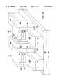
- FIG. 1Ais a perspective view illustrating an inverter according to the teachings of the present invention.
- FIG. 1Bis a top view of the inverter shown in FIG. 1A.
- FIG. 1Cis a schematic diagram illustrating an embodiment of the inverter of FIG. 1A.
- FIGS. 2A-2Jillustrate an embodiment of a process of fabrication of an inverter according to the teachings of the present invention.
- FIG. 3is a block diagram illustrating an information handling system according to an embodiment of the present invention.
- wafer and substrate used in the following descriptioninclude any structure having an exposed surface with which to form the integrated circuit (IC) structure of the invention.
- substrateis understood to include semiconductor wafers.
- substrateis also used to refer to semiconductor structures during processing, and may include other layers that have been fabricated thereupon. Both wafer and substrate include doped and undoped semiconductors, epitaxial semiconductor layers supported by a base semiconductor or insulator, as well as other semiconductor structures well known to one skilled in the art.
- conductoris understood to include semiconductors
- insulatoris defined to include any material that is less electrically conductive than the materials referred to as conductors.
- horizontalas used in this application is defined as a plane parallel to the conventional plane or surface of a wafer or substrate, regardless of the orientation of the wafer or substrate.
- verticalrefers to a direction perpendicular to the horizonal as defined above. Prepositions, such as “on”, “side” (as in “sidewall”), “higher”, “lower”, “over” and “under” are defined with respect to the conventional plane or surface being on the top surface of the wafer or substrate, regardless of the orientation of the wafer or substrate.
- n+refers to semiconductor material that is heavily doped n-type semiconductor material, e.g., monocrystalline silicon or polycrystalline silicon.
- p+refers to semiconductor material that is heavily doped p-type semiconductor material.
- n- and p-refer to lightly doped n and p-type semiconductor materials, respectively.
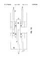
- FIG. 1Ais a perspective view illustrating generally an embodiment of a portion of an inverter according to the teachings of the present invention.
- inverter 50is a two transistor device that is formed using, for example, the technique described below with respect to FIGS. 2A through 2J.
- the inverteris formed from a complementary pair of gate body transistors.
- the complementary pairincludes a first channel type transistor and a second channel type transistor.
- Each transistor in inverter 50is either an n-channel metal-oxide semiconductor (NMOS) or a p-channel metal-oxide semiconductor (PMOS).
- NMOSn-channel metal-oxide semiconductor
- PMOSp-channel metal-oxide semiconductor
- the inverter 50includes one NMOS transistor Q 2 and one PMOS transistor Q 1 .
- Each NMOS and PMOS transistorincludes a body region, 110 and 105 respectively, formed of single crystalline semiconductor material that extends outwardly from a substrate.
- the body regions 110 and 105have an upper surface 112 and opposing sidewalls 111.
- the NMOS body region 110is formed of p- silicon material and the PMOS body region 105 is formed of n- silicon material.
- the substrate 100is p- silicon material.
- the NMOS and PMOS body regions, 110 and 105 respectivelyare formed on an insulator layer 180 formed on the substrate 100.
- the NMOS and PMOS transistorsinclude source regions, 106 and 108 respectively, formed within the upper surface 112 of the body regions, 110 and 105 respectively.
- each of the NMOS and PMOS transistorsinclude a drain region, 107 and 109 respectively, formed within the upper surface 112 of the body regions, 110 and 105 respectively.
- a dielectric layer 120is formed on the upper surface 112 and on portions of the opposing sidewalls 111 for the NMOS and PMOS transistors.
- the NMOS transistor Q 2includes a gate 130 on the dielectric layer 120.
- the PMOS transistor Q 1includes a gate 131 formed on the dielectric layer 120. In one embodiment, gate 131 is formed of p+ silicon material and gate 130 is formed of n+ silicon material.
- the NMOS transistor Q 2includes conductive sidewall members 140.
- the PMOS transistors Q 1similarly includes conductive sidewall members 145. In one embodiment, the conductive sidewall members 140 are formed of p+ silicon material and the conductive sidewall members 145 are formed of n+ silicon material.
- Conductive sidewall members, 140 and 145 respectivelyare disposed adjacent to portions of the dielectric layer 120 formed on the opposing sidewall surfaces 111.
- the conductive sidewall members, 140 and 145 respectivelycouple to the gates, 130 and 131 respectively, of the NMOS and PMOS transistors.
- the conductive sidewall members, 140 and 145 respectivelyfurther couple to a portion of the opposing sidewalls 111 of the NMOS and PMOS transistors such that the transistors give metal-oxide semiconductor (MOS) type conduction and bipolar junction transistor (BJT) type conduction underneath the gates, 130 and 131 respectively.
- the conductive sidewall members, 140 and 145 respectivelyare formed of polysilicon.
- Inverter 50also includes a gate contact 160.
- Gate contact 160couples to gate 130 of transistor Q 2 through a refractory metal 132.
- Gate contact 160couples to gate 131 of transistor Q 1 through a refractory metal 132.
- the gate contact 160provides an input to the inverter 50.
- the inverter 50includes an electrical contact 162 between the drain regions, 107 and 109, to provide an output for the inverter 50.
- the source region 106 of transistor Q 2is coupled to ground and the source region 108 of transistor Q 1 is coupled to the power supply V dd .
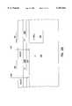
- FIG. 1Bis a top view of the embodiment of FIG. 1A.
- FIG. 1Billustrates the gate contact 160 serving as the input to the inverter 50 and the electrical contact 162 serving as the output for the inverter 50.
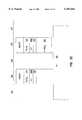
- FIG. 1Cis a schematic diagram of the inverter shown in FIG. 1A. The operation of the embodiment of FIG. 1A is described in connection with the schematic diagram of FIG. 1C.
- inverter 50receives a "high” or “low” voltage input corresponding to a logic “1” or logic “0". The voltage input is coupled to the gate contact 160.
- the input on the gate contact 160is simultaneously coupled to the gates, 130 and 131, and to the body regions, 110 and 105, of the NMOS and PMOS transistors through the conductive sidewall members, 140 and 145 respectively.
- the structurecombines metal-oxide semiconductor (MOS) conduction underneath the gate with bipolar junction transistor (BJT) conduction in the body region, 110 or 105, of the activated transistor.
- MOSmetal-oxide semiconductor
- BJTbipolar junction transistor
- the “merged” conductionin effect reduces the voltage threshold level (V t ) for turning on the transistor and results in quicker activation or switching speed for the "triggered" transistor.
- Conduction in the body region, 110 or 105, of either the NMOS or PMOS transistorscouples the source region, 106 or 108, and the drain region, 107 or 109, within the same transistor.
- the source regions, 106 and 108, of the NMOS and PMOS transistorsare both electrically connected to external potential levels.
- the potential level connected to the conducting transistoris carried to the associated drain region, 107 or 109, and to the electrical contact 162 which serves as the output to the inverter.
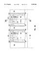
- FIGS. 2A through 2Jillustrate an embodiment of the various processing steps for fabricating a inverter formed from a complementary pair of gate-body transistors.
- FIG. 2Abegins with a lightly doped p- silicon substrate 200.
- a thin oxide pad layeris grown and then additional oxide is deposited on the substrate, such as by chemical vapor deposition (CVD), to form oxide layer 220.
- the oxide layer 220is formed to a thickness of approximately 0.2 micrometers ( ⁇ m).
- a photoresistis applied and selectively exposed to reveal p-channel metal oxide semiconductor (PMOS) device region 221.
- the oxide layer 220is etched from the PMOS device regions 221, such as by reactive ion etching (RIE).
- RIEreactive ion etching
- n-wells 225 of n-type materialare formed in the substrate 200 to form the PMOS device regions 221.
- the n-wells 225 of n-type materialcan be formed by any suitable method, such as by ion implantation.
- the n-wells 225are formed to a thickness of approximately 0.4 ⁇ m.
- the photoresistis removed using conventional photoresist stripping techniques. The structure is now as it appears in FIG. 2A.
- FIG. 2Billustrates the structure after the next sequence of processing steps.
- the oxide layer 220is stripped, such as by RIE and a fresh gate oxide 250 is themally grown on and across the upper surface 245 of the n-well 225 and the p-substrate 200.
- a p+ polysilicon gate material 260Ais deposited across the surface of the oxide layer 250.
- the p+ layer 260Ais formed to a thickness of approximately 0.2 ⁇ m.
- the p+layer 260Acan be deposited through any suitable method, such as through chemical vapor deposition (CVD).
- a photoresistis applied and selectively exposed to provide a mask-defining an n-channel metaloxide semiconductor (NMOS) device region 222.
- NMOSn-channel metaloxide semiconductor
- n+ polysilicon gate material 260Bis formed in the NMOS device region 222 through a process such as ion implantation of n-type impurity ions.
- the n+ dopantis Arsenic (As). The structure is now as appears in FIG. 2B.
- FIG. 2Cillustrates the structure after the next sequence of processing steps.
- the photoresistis stripped, using conventional photoresist stripping techniques.
- a nitride pad 270is formed on and across the surface of the n+ gate material 260B and the p+ gate material 260A.
- the nitride pad 270is deposited by any suitable process, such as chemical vapor deposition (CVD).
- the nitride padis deposited to a thickness of approximately 0.4 ⁇ m.
- a photoresistis applied and selectively exposed to provide a mask which defines and covers the PMOS and NMOS device regions, 221 and 222 respectively.
- the nitride cap 270is removed by any suitable etching technique, such as by RIE.
- the p+ gate material 260A in between device regions, 221 and 222,is removed.
- the gate oxide 250 in between device regions, 221 and 222,is removed.
- Each of these materialscan be removed by etching using the RIE technique.
- the etching processis continued into the p- substrate 200 to a depth of approximately 0.2 ⁇ m below the bottom of the n-well 225/substrate 200 interface.
- the etchingis performed through any suitable process, such as by RIE. These etching steps leave trenches 242 between the device regions 221 and 222.
- the structureis now as shown in FIG. 2C.
- the photoresistis next stripped, using conventional photoresist stripping techniques.
- FIG. 2Dillustrates the structure after the next series of processing steps.
- An insulator layer 280is formed beneath the device regions, 221 and 222 respectively so as to form a semiconductor on insulator (SOI) structure.
- the insulator layer 280is formed using, for example, the techniques of U.S. application Ser. No. 08/745,708, entitled Silicon-On-Insulator Islands and Method for Their Formation (the '708 Application), or U.S. Pat. No. 5,691,230, entitled Technique for Producing Small Islands of Silicon on Insulator (the '230 Patent).
- the '708 Application and the '230 Patentare incorporated by reference.
- the insulator layer 280separates from substrate 200 the p- single crystalline silicon structure 205 of the NMOS device region 222, and the n-well 225 single crystalline silicon structure of the PMOS device region 221.
- intrinsic polysilicon 290is deposited by any suitable methods, such as by CVD, to fill the trenches 242.
- the intrinsic polysilicon 290 in trenches 242can be planarized by any suitable process, such as by chemical mechanical polishing/planarization (CMP) stopping on the nitride pads 270.
- CMPchemical mechanical polishing/planarization
- the intrinsic polysilicon 290is directionally etched back to leave approximately 0.1-0.2 ⁇ m on the bottom of the trenches 242.
- the etchcan be performed using any suitable method such as reactive ion etching (RIE).
- Oxide 291is deposited such as by CVD to fill trenches 242.
- the oxide 291is etched back approximately 0.4 ⁇ m to the level of the top of the gates 260.
- a nitride spacer 295is deposited such as by CVD.
- the nitride spacer 295is directionally etched to leave on the exposed vertical sidewalls of the nitride pad 270.
- the structureis now as shown in FIG. 2D.
- FIG. 2Eillustrates the structure following the next sequence of process steps.
- the oxide 291 and the intrinsic polysilicon 290are directionally etched using the nitride spacer 295 overhang as a mask.
- An n+ polysilicon layer 294Ais deposited by CVD.
- the n+ polysilicon 294Ais etched, such as by reactive ion etching, to leave on the vertical sidewalls of the oxide spacer 291.
- the n+ polysilicon layer 294Aserves as the conductive sidewall members for the PMOS device region 221.
- the structureis now as shown in FIG. 2E.
- FIG. 2Fillustrates the structure after the next sequence of process steps.
- Silicon dioxide 292is deposited in the trenches 242 and then planarized using CMP.
- the silicon dioxide 292may be deposited by any suitable method, such as by CVD.
- a photoresistis applied and selectively exposed to reveal only the NMOS device regions 222.
- the exposed n+ polysilicon 294Ais selectively etched to remove from the sidewalls of the NMOS device regions 222.
- a p+ polysilicon layer 294Bis then deposited by CVD to fill the slots left from removal of the n+ polysilicon 294A and is then removed from the top surface by any suitable method, such as RIE or CMP.
- the p+ polysilicon layer 294Bserves as the conductive sidewall members for the NMOS device region 222.
- the structureis now as shown in FIG. 2F.
- FIG. 2Gillustrates the structure following the next sequence of process steps.
- a phosphoric acidis applied to remove the nitride cap 270 and the nitride spacer 295 from the active device regions, 221 and 222 respectively. Removal of the nitride cap 270 and the nitride spacer 295 exposes the p+ and n+ gate material, 260A and 260B respectively.
- a gate contact 296is deposited, such as by CVD, over the p+ and n+ gate regions, 260A and 260B respectively. In one embodiment, the gate contact 296 is formed of tungsten (W). In another embodiment, the gate contact 296 is any other suitable refractory metal.
- the gate contact 296is planarized, such as by CMP, such that the gate contact 296 is left only over the p+ and n+ gate regions, 260A and 260B respectively. The device is now as shown in FIG. 2G.
- FIG. 2His a cross sectional view along cut line 2H--2H of FIG. 2G.
- FIG. 2Hillustrates the structure after the following sequence of process steps.
- a photoresistis applied and selectively exposed to mask the gate regions 244.
- the gate contact 296 material and the n+ or p+ polysilicon gate material, 260B and 260A, which remain exposedare etched to the underlying gate oxide 250 and insulator layer 280.
- the etchingmay be performed using RIE.
- the structureis now as is shown in FIG. 2H.
- FIG. 2Iis a top view of FIG. 2H.
- the p+ or n+ polysilicon layers 294B and 294A, located between the device regions 221 and 222,are removed by etching.
- the etchingcan be performed using any suitable method, such as RIE.
- FIG. 2Jillustrates the structure following the next series of process steps.
- the photoresistis removed using conventional photoresist stripping techniques.
- An annealis performed to out diffuse boron from the p- layer 205 and to out diffuse Arsenic (As) from the n-well 225.
- the annealalso serves to out diffuse the dopants from the p+ and n+ polysilicon layers, 294B and 294A respectively.
- the annealingserves to dope the adjoining sandwiched intrinsic polysilicon 290. Boron and Arsenic, respectively, will out diffuse into the intrinsic polysilicon 290 in approximately equal amounts.
- This process stepeffectively enhances the thickness of the p+ and n+ polysilicon conductive sidewall members, 294B and 294A respectively.
- a photoresistis applied and exposed to cover the NMOS gate-body transistor 51. Then, a p+ source region 298A and a drain region 299A are ion implanted using self-aligning process techniques with the gate 260A. The photoresist is then stripped using conventional photoresist stripping techniques.
- Another photoresistis applied and exposed, this time to cover the PMOS gate-body transistor 52.
- Another ion implantation stepis used to form an n+ source region 298B and a drain region 299B in the NMOS gate-body transistor 52.
- the photoresistis once again removed.
- the structureis now as shown in FIG. 2J.
- the remaining contact holes and wiring required to form the inverter 50are achieved through conventional metallization processing steps. These steps are recited here in reference to FIG. 1A and FIG. 2J.
- the NMOS and PMOS transistors, 51 and 52respectfully, form an inverter equivalent to the embodiment of inverter 104 or inverter 105 as shown in FIG. 1A. Accordingly, the NMOS transistor 51 interchangeably represents transistors Q 2 or Q 4 shown in FIG. 1A.
- the PMOS transistor 52equally represents transistors Q 1 and Q 3 shown in FIG. 1A.
- metal shunt 162is formed, through standard metallization processing, to connect drain regions, 107 and 109 in FIG. 1A or 299A and 299B of FIG. 2J.
- Gate contact 160is formed to couple the gates of NMOS and PMOS transistors, 51 and 52 in FIG. 2J or Q 2 and Q 1 of FIG. 1A. Gate contact 160 is cross-coupled to a similar metal shunt 163 on the drain regions of inverter 104. A gate contact 161, formed to couple the gates of NMOS and PMOS transitors Q 3 and Q 4 , is cross-coupled to metal shunt 162.
- the cross-coupled gate contacts and metal shunts, 160, 163, 161 and 162 respectively,include contacts to input/output lines 150 and 152 via conventional processing techniques. Bit lines are coupled to the inputs or source/drain regions, 106/298B, of the NMOS transistors, Q 2 or Q 4 respectively.
- a supply potentialis coupled to both inputs or source/drain regions, 108/298A, of the PMOS transistors, Q 1 and Q 3 respectively. This conventional metallization process is not recited here.
- FIG. 3is a block diagram illustrating an information handling system 300 according to an embodiment of the present invention.
- the information handling systemincludes a central processing unit (CPU) 304.
- the central processing unit 304is coupled to a memory unit 330 by a system bus 310.
- the memory unit 330is a random access memory (RAM).
- the central processing unitcan be constructed to include the inverter structure embodiment presented above.
- the inverter structureincludes gate-body transistors which have opposing sidewalls and adjacent conductive sidewall members to conserve available surface space on a semiconductor chip. Conservation of surface space achieves a higher density of surface structures per chip.
- the structuresoffer performance advantages from both metal-oxide semiconductor (MOS) and bipolar junction transistor (BJT) designs.
- MOSmetal-oxide semiconductor
- BJTbipolar junction transistor
- the devicescan be used in a variety of applications, digital and analog, wherever a more compact structure with low power consumption and fast response time is needed.
Landscapes
- Metal-Oxide And Bipolar Metal-Oxide Semiconductor Integrated Circuits (AREA)
Abstract
Description
Claims (19)
Priority Applications (2)
| Application Number | Priority Date | Filing Date | Title |
|---|---|---|---|
| US09/050,579US6107663A (en) | 1998-03-30 | 1998-03-30 | Circuit and method for gate-body structures in CMOS technology |
| US09/323,493US6060754A (en) | 1998-03-30 | 1999-06-01 | Circuit and method for gate-body structures in CMOS technology |
Applications Claiming Priority (1)
| Application Number | Priority Date | Filing Date | Title |
|---|---|---|---|
| US09/050,579US6107663A (en) | 1998-03-30 | 1998-03-30 | Circuit and method for gate-body structures in CMOS technology |
Related Child Applications (1)
| Application Number | Title | Priority Date | Filing Date |
|---|---|---|---|
| US09/323,493ContinuationUS6060754A (en) | 1998-03-30 | 1999-06-01 | Circuit and method for gate-body structures in CMOS technology |
Publications (1)
| Publication Number | Publication Date |
|---|---|
| US6107663Atrue US6107663A (en) | 2000-08-22 |
Family
ID=21966081
Family Applications (2)
| Application Number | Title | Priority Date | Filing Date |
|---|---|---|---|
| US09/050,579Expired - LifetimeUS6107663A (en) | 1998-03-30 | 1998-03-30 | Circuit and method for gate-body structures in CMOS technology |
| US09/323,493Expired - LifetimeUS6060754A (en) | 1998-03-30 | 1999-06-01 | Circuit and method for gate-body structures in CMOS technology |
Family Applications After (1)
| Application Number | Title | Priority Date | Filing Date |
|---|---|---|---|
| US09/323,493Expired - LifetimeUS6060754A (en) | 1998-03-30 | 1999-06-01 | Circuit and method for gate-body structures in CMOS technology |
Country Status (1)
| Country | Link |
|---|---|
| US (2) | US6107663A (en) |
Cited By (9)
| Publication number | Priority date | Publication date | Assignee | Title |
|---|---|---|---|---|
| US6340612B1 (en)* | 1998-03-30 | 2002-01-22 | Micron Technology, Inc. | Method of fabricating body contacted and backgated transistors |
| US6365448B2 (en) | 1998-03-30 | 2002-04-02 | Micron Technology, Inc. | Structure and method for gated lateral bipolar transistors |
| US6376317B1 (en) | 1998-03-30 | 2002-04-23 | Micron Technology, Inc. | Methods for dual-gated transistors |
| US6451656B1 (en) | 2001-02-28 | 2002-09-17 | Advanced Micro Devices, Inc. | CMOS inverter configured from double gate MOSFET and method of fabricating same |
| US6696330B2 (en) | 1998-02-26 | 2004-02-24 | Micron Technology, Inc. | Methods, structures, and circuits for transistors with gate-to-body capacitive coupling |
| US20050020020A1 (en)* | 2002-07-16 | 2005-01-27 | Nadine Collaert | Integrated semiconductor fin device and a method for manufacturing such device |
| SG135930A1 (en)* | 2002-12-06 | 2007-10-29 | Taiwan Semiconductor Mfg | Cmos inverters configured using multiple-gate transistors |
| US20150263726A1 (en)* | 2014-03-17 | 2015-09-17 | Stmicroelectronics International N.V. | Novel methodology to avoid gate stress for low voltage devices in fdsoi technology |
| WO2023197769A1 (en)* | 2022-04-15 | 2023-10-19 | 华为技术有限公司 | Cmos inverter, storage chip, memory and electronic device |
Citations (22)
| Publication number | Priority date | Publication date | Assignee | Title |
|---|---|---|---|---|
| US4450048A (en)* | 1982-07-09 | 1984-05-22 | U.S. Philips Corporation | Method of manufacturing capacitors integrated in microelectronic structure |
| US4673962A (en)* | 1985-03-21 | 1987-06-16 | Texas Instruments Incorporated | Vertical DRAM cell and method |
| US4922315A (en)* | 1987-11-13 | 1990-05-01 | Kopin Corporation | Control gate lateral silicon-on-insulator bipolar transistor |
| US4987089A (en)* | 1990-07-23 | 1991-01-22 | Micron Technology, Inc. | BiCMOS process and process for forming bipolar transistors on wafers also containing FETs |
| US4996574A (en)* | 1988-07-01 | 1991-02-26 | Fujitsu Limited | MIS transistor structure for increasing conductance between source and drain regions |
| US5006909A (en)* | 1989-10-30 | 1991-04-09 | Motorola, Inc. | Dram with a vertical capacitor and transistor |
| US5097381A (en)* | 1990-10-11 | 1992-03-17 | Micron Technology, Inc. | Double sidewall trench capacitor cell |
| US5122848A (en)* | 1991-04-08 | 1992-06-16 | Micron Technology, Inc. | Insulated-gate vertical field-effect transistor with high current drive and minimum overlap capacitance |
| US5250450A (en)* | 1991-04-08 | 1993-10-05 | Micron Technology, Inc. | Insulated-gate vertical field-effect transistor with high current drive and minimum overlap capacitance |
| US5315143A (en)* | 1992-04-28 | 1994-05-24 | Matsushita Electric Industrial Co., Ltd. | High density integrated semiconductor device |
| US5350934A (en)* | 1992-03-05 | 1994-09-27 | Kabushiki Kaisha Toshiba | Conductivity modulation type insulated gate field effect transistor |
| US5379255A (en)* | 1992-12-14 | 1995-01-03 | Texas Instruments Incorporated | Three dimensional famos memory devices and methods of fabricating |
| US5491356A (en)* | 1990-11-19 | 1996-02-13 | Micron Technology, Inc. | Capacitor structures for dynamic random access memory cells |
| US5528062A (en)* | 1992-06-17 | 1996-06-18 | International Business Machines Corporation | High-density DRAM structure on soi |
| US5581104A (en)* | 1991-01-16 | 1996-12-03 | Micron Technology, Inc. | Static discharge circuit having low breakdown voltage bipolar clamp |
| US5585998A (en)* | 1995-12-22 | 1996-12-17 | International Business Machines Corporation | Isolated sidewall capacitor with dual dielectric |
| US5646900A (en)* | 1995-01-12 | 1997-07-08 | Mitsubishi Denki Kabushiki Kaisha | Sense amplifier including MOS transistors having threshold voltages controlled dynamically in a semiconductor memory device |
| US5680345A (en)* | 1995-06-06 | 1997-10-21 | Advanced Micro Devices, Inc. | Nonvolatile memory cell with vertical gate overlap and zero birds beaks |
| US5691230A (en)* | 1996-09-04 | 1997-11-25 | Micron Technology, Inc. | Technique for producing small islands of silicon on insulator |
| US5796166A (en)* | 1995-01-12 | 1998-08-18 | Ibm Corporation | Tasin oxygen diffusion barrier in multilayer structures |
| US5796143A (en)* | 1996-10-30 | 1998-08-18 | Advanced Micro Devices, Inc. | Trench transistor in combination with trench array |
| US5892260A (en)* | 1995-01-27 | 1999-04-06 | Nec Corporation | SOI-type semiconductor device with variable threshold voltages |
Family Cites Families (3)
| Publication number | Priority date | Publication date | Assignee | Title |
|---|---|---|---|---|
| JPH07105447B2 (en)* | 1988-12-15 | 1995-11-13 | 株式会社東芝 | Transmission gate |
| JP2994670B2 (en)* | 1989-12-02 | 1999-12-27 | 忠弘 大見 | Semiconductor device and manufacturing method thereof |
| US5554870A (en)* | 1994-02-04 | 1996-09-10 | Motorola, Inc. | Integrated circuit having both vertical and horizontal devices and process for making the same |
- 1998
- 1998-03-30USUS09/050,579patent/US6107663A/ennot_activeExpired - Lifetime
- 1999
- 1999-06-01USUS09/323,493patent/US6060754A/ennot_activeExpired - Lifetime
Patent Citations (24)
| Publication number | Priority date | Publication date | Assignee | Title |
|---|---|---|---|---|
| US4450048A (en)* | 1982-07-09 | 1984-05-22 | U.S. Philips Corporation | Method of manufacturing capacitors integrated in microelectronic structure |
| US4673962A (en)* | 1985-03-21 | 1987-06-16 | Texas Instruments Incorporated | Vertical DRAM cell and method |
| US4922315A (en)* | 1987-11-13 | 1990-05-01 | Kopin Corporation | Control gate lateral silicon-on-insulator bipolar transistor |
| US4996574A (en)* | 1988-07-01 | 1991-02-26 | Fujitsu Limited | MIS transistor structure for increasing conductance between source and drain regions |
| US5006909A (en)* | 1989-10-30 | 1991-04-09 | Motorola, Inc. | Dram with a vertical capacitor and transistor |
| US4987089A (en)* | 1990-07-23 | 1991-01-22 | Micron Technology, Inc. | BiCMOS process and process for forming bipolar transistors on wafers also containing FETs |
| US5097381A (en)* | 1990-10-11 | 1992-03-17 | Micron Technology, Inc. | Double sidewall trench capacitor cell |
| US5491356A (en)* | 1990-11-19 | 1996-02-13 | Micron Technology, Inc. | Capacitor structures for dynamic random access memory cells |
| US5581104A (en)* | 1991-01-16 | 1996-12-03 | Micron Technology, Inc. | Static discharge circuit having low breakdown voltage bipolar clamp |
| US5122848A (en)* | 1991-04-08 | 1992-06-16 | Micron Technology, Inc. | Insulated-gate vertical field-effect transistor with high current drive and minimum overlap capacitance |
| US5250450A (en)* | 1991-04-08 | 1993-10-05 | Micron Technology, Inc. | Insulated-gate vertical field-effect transistor with high current drive and minimum overlap capacitance |
| US5350934A (en)* | 1992-03-05 | 1994-09-27 | Kabushiki Kaisha Toshiba | Conductivity modulation type insulated gate field effect transistor |
| US5315143A (en)* | 1992-04-28 | 1994-05-24 | Matsushita Electric Industrial Co., Ltd. | High density integrated semiconductor device |
| US5541432A (en)* | 1992-04-28 | 1996-07-30 | Matsushita Electric Industrial Co., Ltd. | Silicon on insulator field effect transistors |
| US5528062A (en)* | 1992-06-17 | 1996-06-18 | International Business Machines Corporation | High-density DRAM structure on soi |
| US5508544A (en)* | 1992-12-14 | 1996-04-16 | Texas Instruments Incorporated | Three dimensional FAMOS memory devices |
| US5379255A (en)* | 1992-12-14 | 1995-01-03 | Texas Instruments Incorporated | Three dimensional famos memory devices and methods of fabricating |
| US5646900A (en)* | 1995-01-12 | 1997-07-08 | Mitsubishi Denki Kabushiki Kaisha | Sense amplifier including MOS transistors having threshold voltages controlled dynamically in a semiconductor memory device |
| US5796166A (en)* | 1995-01-12 | 1998-08-18 | Ibm Corporation | Tasin oxygen diffusion barrier in multilayer structures |
| US5892260A (en)* | 1995-01-27 | 1999-04-06 | Nec Corporation | SOI-type semiconductor device with variable threshold voltages |
| US5680345A (en)* | 1995-06-06 | 1997-10-21 | Advanced Micro Devices, Inc. | Nonvolatile memory cell with vertical gate overlap and zero birds beaks |
| US5585998A (en)* | 1995-12-22 | 1996-12-17 | International Business Machines Corporation | Isolated sidewall capacitor with dual dielectric |
| US5691230A (en)* | 1996-09-04 | 1997-11-25 | Micron Technology, Inc. | Technique for producing small islands of silicon on insulator |
| US5796143A (en)* | 1996-10-30 | 1998-08-18 | Advanced Micro Devices, Inc. | Trench transistor in combination with trench array |
Non-Patent Citations (40)
| Title |
|---|
| Chen, M.J., et al., "Back-Gate Forward Bias Method for Low-Voltage CMOS Digital Cicuits", IEEE Transactions of Electron Devices, 43, 904-909, (Jun. 1986). |
| Chen, M.J., et al., "Optimizing the Match in Weakly Inverted Mosfet's by Gated Lateral Bipolar Action", IEEE Transactions on Electron Devices, 43, 766-773, (May 1996). |
| Chen, M.J., et al., Back Gate Forward Bias Method for Low Voltage CMOS Digital Cicuits , IEEE Transactions of Electron Devices , 43, 904 909, (Jun. 1986).* |
| Chen, M.J., et al., Optimizing the Match in Weakly Inverted Mosfet s by Gated Lateral Bipolar Action , IEEE Transactions on Electron Devices , 43, 766 773, (May 1996).* |
| Chung, I.Y., et al., "A New SOI Inverter for Low Power Applications", Proceedings of the 1996 IEEE International SOI Conference, Sanibel Island, FL, 20-21, (Sep. 30-Oct. 3, 1996). |
| Chung, I.Y., et al., A New SOI Inverter for Low Power Applications , Proceedings of the 1996 IEEE International SOI Conference , Sanibel Island, FL, 20 21, (Sep. 30 Oct. 3, 1996).* |
| Denton, J.P., et al., "Fully Depleted Dual-Gated Thin-Film SOI P-Mosfet's Fabricated in SOI Islands with an Isolated Buried Polysilicon Backgate", IEEE Electron Device Letters, 17, 509-511, (Nov. 1996). |
| Denton, J.P., et al., Fully Depleted Dual Gated Thin Film SOI P Mosfet s Fabricated in SOI Islands with an Isolated Buried Polysilicon Backgate , IEEE Electron Device Letters , 17, 509 511, (Nov. 1996).* |
| Fuse, T., et al., "A 0.5V 200MHz 1-Stage 32b ALU Using a Body Bias Controlled SOI Pass-Gate Logic", 1997 IEEE International Solid-State Circuits Conference, Digest of Technical Papers, 286-287, (1997). |
| Fuse, T., et al., A 0.5V 200MHz 1 Stage 32b ALU Using a Body Bias Controlled SOI Pass Gate Logic , 1997 IEEE International Solid State Circuits Conference, Digest of Technical Papers , 286 287, (1997).* |
| Holman, W.T., et al., "A Compact Low Noise Operational Amplifier for a 1.2 Micrometer Digital CMOS Technology", IEEE Journal of Solid-State Circuits, 30, 710-714, (Jun. 1995). |
| Holman, W.T., et al., A Compact Low Noise Operational Amplifier for a 1.2 Micrometer Digital CMOS Technology , IEEE Journal of Solid State Circuits , 30, 710 714, (Jun. 1995).* |
| Horiguchi, et al., "Switched-Source-Impedance CMOS Circuit for Low Standby Subthreshold Current Giga-Scale LSIs", IEEE Journal of Solid State Circuits, vol. 28, 1131-1135, (1993). |
| Horiguchi, et al., Switched Source Impedance CMOS Circuit for Low Standby Subthreshold Current Giga Scale LSIs , IEEE Journal of Solid State Circuits , vol. 28, 1131 1135, (1993).* |
| Huang, W. L., et al., "TFSOI Complementary BiCMOS Technology for Low Power Applications", IEEE Transactions on Electron Devices, 42, 506-512, (Mar. 1995). |
| Huang, W. L., et al., TFSOI Complementary BiCMOS Technology for Low Power Applications , IEEE Transactions on Electron Devices , 42, 506 512, (Mar. 1995).* |
| Jaeger, et al., "A High-speed Sensing Scheme for 1T Dynamic RAMs Utilizing the Clamped Bit-line Sense Amplifier", IEEE Journal of Solid State Circuits, vol. 27, 618-25, (1992). |
| Jaeger, et al., A High speed Sensing Scheme for 1T Dynamic RAMs Utilizing the Clamped Bit line Sense Amplifier , IEEE Journal of Solid State Circuits , vol. 27, 618 25, (1992).* |
| Ko, et al., "High-gain Lateral Bipolar Action in a Mosfet Structure", IEEE Trans. on Electron Devices, vol. 38, No. 11, 2487-96, (Nov. 1991). |
| Ko, et al., High gain Lateral Bipolar Action in a Mosfet Structure , IEEE Trans. on Electron Devices, vol. 38, No. 11 , 2487 96, (Nov. 1991).* |
| MacSweeney, D., et al., "Modelling of Lateral Bipolar Devices in a CMOS Process", IEEE Bipolar Circuits and Technology Meeting, Minneapolis, MN, 27-30, (Sep. 1996). |
| MacSweeney, D., et al., Modelling of Lateral Bipolar Devices in a CMOS Process , IEEE Bipolar Circuits and Technology Meeting , Minneapolis, MN, 27 30, (Sep. 1996).* |
| Parke, S.A., et al., "A High-Performance Lateral Bipolar Transistor Fabricated on Simox", IEEE Electron Device Letters, 14, 33-35, (Jan. 1993). |
| Parke, S.A., et al., A High Performance Lateral Bipolar Transistor Fabricated on Simox , IEEE Electron Device Letters , 14, 33 35, (Jan. 1993).* |
| Rabaey, Digital Integrated Circuits , Prentice Hall, Englewood Cliffs, NJ, 222 232, (1996).* |
| Rabaey, Digital Integrated Circuits, Prentice Hall, Englewood Cliffs, NJ, 222-232, (1996). |
| Saito, M., et al., "Technique for Controlling Effective Vth in Multi-Gbit DRAM Sense Amplifier", 1996 Symposium on VLSI Circuits, Digest of Technical Papers, Honolulu, HI, 106-107, (Jun. 13-15, 1996). |
| Saito, M., et al., Technique for Controlling Effective Vth in Multi Gbit DRAM Sense Amplifier , 1996 Symposium on VLSI Circuits, Digest of Technical Papers , Honolulu, HI, 106 107, (Jun. 13 15, 1996).* |
| Seevinck, E., et al., "Current-Mode Techniques for High-Speed VLSI Circuits with Applications to Current Sense Amplifier for CMOS SRAM's", IEEE Journal of Solid-State Circuits, 26, 525-536, (Apr. 1991). |
| Seevinck, E., et al., Current Mode Techniques for High Speed VLSI Circuits with Applications to Current Sense Amplifier for CMOS SRAM s , IEEE Journal of Solid State Circuits , 26, 525 536, (Apr. 1991).* |
| Shimomura, K., et al., "A 1V 46ns 16Mb SOI-DRAM with Body Control Technique", 1997 IEEE International Solid-State Circuits Conference, Digest of Technical Papers, 68-69, (Feb. 6, 1997). |
| Shimomura, K., et al., A 1V 46ns 16Mb SOI DRAM with Body Control Technique , 1997 IEEE International Solid State Circuits Conference, Digest of Technical Papers , 68 69, (Feb. 6, 1997).* |
| Tsui, P.G., et al., "A Versatile Half-Micron Complementary BiCMOS Technology for Microprocessor-Based Smart Power Applications", IEEE Transactions on Electron Devices, 42, 564-570, (Mar. 1995). |
| Tsui, P.G., et al., A Versatile Half Micron Complementary BiCMOS Technology for Microprocessor Based Smart Power Applications , IEEE Transactions on Electron Devices , 42, 564 570, (Mar. 1995).* |
| Tuinega, A Guide to Circuit Simulation and Analysis Using PSPICE , Prentice Hall, Englewood Cliffs, NJ, (1988).* |
| Tuinega, A Guide to Circuit Simulation and Analysis Using PSPICE, Prentice Hall, Englewood Cliffs, NJ, (1988). |
| Wolf, S., In: Silicon Processing for the VLSI Era, vol. 2 , Lattice Press, Sunset Beach, CA, 389 392, (1990).* |
| Wolf, S., In: Silicon Processing for the VLSI Era, vol. 2, Lattice Press, Sunset Beach, CA, 389-392, (1990). |
| Wong, et al., "A 1V CMOS Digital Circuits with Double-Gate Driven Mosfet", IEEE Int. Solid State Circuits Conference, San Francisco, 292-93, (1997). |
| Wong, et al., A 1V CMOS Digital Circuits with Double Gate Driven Mosfet , IEEE Int. Solid State Circuits Conference, San Francisco , 292 93, (1997).* |
Cited By (13)
| Publication number | Priority date | Publication date | Assignee | Title |
|---|---|---|---|---|
| US6696330B2 (en) | 1998-02-26 | 2004-02-24 | Micron Technology, Inc. | Methods, structures, and circuits for transistors with gate-to-body capacitive coupling |
| US6340612B1 (en)* | 1998-03-30 | 2002-01-22 | Micron Technology, Inc. | Method of fabricating body contacted and backgated transistors |
| US6365448B2 (en) | 1998-03-30 | 2002-04-02 | Micron Technology, Inc. | Structure and method for gated lateral bipolar transistors |
| US6376317B1 (en) | 1998-03-30 | 2002-04-23 | Micron Technology, Inc. | Methods for dual-gated transistors |
| US6414356B1 (en) | 1998-03-30 | 2002-07-02 | Micron Technology, Inc. | Circuits and methods for dual-gated transistors |
| US6451656B1 (en) | 2001-02-28 | 2002-09-17 | Advanced Micro Devices, Inc. | CMOS inverter configured from double gate MOSFET and method of fabricating same |
| US20050020020A1 (en)* | 2002-07-16 | 2005-01-27 | Nadine Collaert | Integrated semiconductor fin device and a method for manufacturing such device |
| US6974729B2 (en)* | 2002-07-16 | 2005-12-13 | Interuniversitair Microelektronica Centrum (Imec) | Integrated semiconductor fin device and a method for manufacturing such device |
| SG135930A1 (en)* | 2002-12-06 | 2007-10-29 | Taiwan Semiconductor Mfg | Cmos inverters configured using multiple-gate transistors |
| US20150263726A1 (en)* | 2014-03-17 | 2015-09-17 | Stmicroelectronics International N.V. | Novel methodology to avoid gate stress for low voltage devices in fdsoi technology |
| US9385708B2 (en)* | 2014-03-17 | 2016-07-05 | Stmicroelectronics International N.V. | Methodology to avoid gate stress for low voltage devices in FDSOI technology |
| US9929728B2 (en) | 2014-03-17 | 2018-03-27 | Stmicroelectronics International N.V. | Methodology to avoid gate stress for low voltage devices in FDSOI technology |
| WO2023197769A1 (en)* | 2022-04-15 | 2023-10-19 | 华为技术有限公司 | Cmos inverter, storage chip, memory and electronic device |
Also Published As
| Publication number | Publication date |
|---|---|
| US6060754A (en) | 2000-05-09 |
Similar Documents
| Publication | Publication Date | Title |
|---|---|---|
| US6414356B1 (en) | Circuits and methods for dual-gated transistors | |
| US6307235B1 (en) | Another technique for gated lateral bipolar transistors | |
| US4918026A (en) | Process for forming vertical bipolar transistors and high voltage CMOS in a single integrated circuit chip | |
| EP0749165B1 (en) | Thin film transistor in insulated semiconductor substrate and manufacturing method thereof | |
| US6342717B1 (en) | Semiconductor device and method for producing same | |
| JP3111059B2 (en) | Method for fabricating dual gate oxide dual work function CMOS | |
| US6777744B2 (en) | Circuits and methods using vertical, complementary transistors | |
| US6879009B2 (en) | Integrated circuit with MOSFETS having bi-layer metal gate electrodes | |
| US4603468A (en) | Method for source/drain self-alignment in stacked CMOS | |
| US6049496A (en) | Circuit and method for low voltage, current sense amplifier | |
| EP0159483B1 (en) | Method of manufacturing a semiconductor device having a well, e.g. a complementary semiconductor device | |
| KR20010033347A (en) | Silicon-on-insulator configuration which is compatible with bulk cmos architecture | |
| US5294822A (en) | Polycide local interconnect method and structure | |
| US4951113A (en) | Simultaneously deposited thin film CMOS TFTs and their method of fabrication | |
| US5721165A (en) | Method of forming CMOS circuitry | |
| JP2001352077A (en) | SOI field effect transistor | |
| JP3383219B2 (en) | SOI semiconductor device and manufacturing method thereof | |
| US6075272A (en) | Structure for gated lateral bipolar transistors | |
| US6340612B1 (en) | Method of fabricating body contacted and backgated transistors | |
| US6633067B2 (en) | Compact SOI body contact link | |
| US4988638A (en) | Method of fabrication a thin film SOI CMOS device | |
| US6107663A (en) | Circuit and method for gate-body structures in CMOS technology | |
| KR100294640B1 (en) | Silicon double membrane device with floating body effect and its manufacturing method | |
| US6104066A (en) | Circuit and method for low voltage, voltage sense amplifier | |
| US5571745A (en) | Fabrication method of semiconductor device containing n- and p-channel MOSFETs |
Legal Events
| Date | Code | Title | Description |
|---|---|---|---|
| AS | Assignment | Owner name:MICRON TECHNOLOGY, INC., IDAHO Free format text:ASSIGNMENT OF ASSIGNORS INTEREST;ASSIGNORS:NOBLE, WENDELL P.;FORBES, LEONARD;REEL/FRAME:009109/0843;SIGNING DATES FROM 19980318 TO 19980319 | |
| STCF | Information on status: patent grant | Free format text:PATENTED CASE | |
| FEPP | Fee payment procedure | Free format text:PAYOR NUMBER ASSIGNED (ORIGINAL EVENT CODE: ASPN); ENTITY STATUS OF PATENT OWNER: LARGE ENTITY | |
| CC | Certificate of correction | ||
| FPAY | Fee payment | Year of fee payment:4 | |
| FPAY | Fee payment | Year of fee payment:8 | |
| FPAY | Fee payment | Year of fee payment:12 | |
| AS | Assignment | Owner name:U.S. BANK NATIONAL ASSOCIATION, AS COLLATERAL AGENT, CALIFORNIA Free format text:SECURITY INTEREST;ASSIGNOR:MICRON TECHNOLOGY, INC.;REEL/FRAME:038669/0001 Effective date:20160426 Owner name:U.S. BANK NATIONAL ASSOCIATION, AS COLLATERAL AGEN Free format text:SECURITY INTEREST;ASSIGNOR:MICRON TECHNOLOGY, INC.;REEL/FRAME:038669/0001 Effective date:20160426 | |
| AS | Assignment | Owner name:MORGAN STANLEY SENIOR FUNDING, INC., AS COLLATERAL AGENT, MARYLAND Free format text:PATENT SECURITY AGREEMENT;ASSIGNOR:MICRON TECHNOLOGY, INC.;REEL/FRAME:038954/0001 Effective date:20160426 Owner name:MORGAN STANLEY SENIOR FUNDING, INC., AS COLLATERAL Free format text:PATENT SECURITY AGREEMENT;ASSIGNOR:MICRON TECHNOLOGY, INC.;REEL/FRAME:038954/0001 Effective date:20160426 | |
| AS | Assignment | Owner name:U.S. BANK NATIONAL ASSOCIATION, AS COLLATERAL AGENT, CALIFORNIA Free format text:CORRECTIVE ASSIGNMENT TO CORRECT THE REPLACE ERRONEOUSLY FILED PATENT #7358718 WITH THE CORRECT PATENT #7358178 PREVIOUSLY RECORDED ON REEL 038669 FRAME 0001. ASSIGNOR(S) HEREBY CONFIRMS THE SECURITY INTEREST;ASSIGNOR:MICRON TECHNOLOGY, INC.;REEL/FRAME:043079/0001 Effective date:20160426 Owner name:U.S. BANK NATIONAL ASSOCIATION, AS COLLATERAL AGEN Free format text:CORRECTIVE ASSIGNMENT TO CORRECT THE REPLACE ERRONEOUSLY FILED PATENT #7358718 WITH THE CORRECT PATENT #7358178 PREVIOUSLY RECORDED ON REEL 038669 FRAME 0001. ASSIGNOR(S) HEREBY CONFIRMS THE SECURITY INTEREST;ASSIGNOR:MICRON TECHNOLOGY, INC.;REEL/FRAME:043079/0001 Effective date:20160426 | |
| AS | Assignment | Owner name:MICRON TECHNOLOGY, INC., IDAHO Free format text:RELEASE BY SECURED PARTY;ASSIGNOR:U.S. BANK NATIONAL ASSOCIATION, AS COLLATERAL AGENT;REEL/FRAME:047243/0001 Effective date:20180629 | |
| AS | Assignment | Owner name:MICRON TECHNOLOGY, INC., IDAHO Free format text:RELEASE BY SECURED PARTY;ASSIGNOR:MORGAN STANLEY SENIOR FUNDING, INC., AS COLLATERAL AGENT;REEL/FRAME:050937/0001 Effective date:20190731 |