US6107105A - Amorphous tin films for an integrated capacitor dielectric/bottom plate using high dielectric constant material - Google Patents
Amorphous tin films for an integrated capacitor dielectric/bottom plate using high dielectric constant materialDownload PDFInfo
- Publication number
- US6107105A US6107105AUS08/868,651US86865197AUS6107105AUS 6107105 AUS6107105 AUS 6107105AUS 86865197 AUS86865197 AUS 86865197AUS 6107105 AUS6107105 AUS 6107105A
- Authority
- US
- United States
- Prior art keywords
- layer
- tin
- forming
- recited
- dielectric material
- Prior art date
- Legal status (The legal status is an assumption and is not a legal conclusion. Google has not performed a legal analysis and makes no representation as to the accuracy of the status listed.)
- Expired - Lifetime
Links
Images
Classifications
- H—ELECTRICITY
- H10—SEMICONDUCTOR DEVICES; ELECTRIC SOLID-STATE DEVICES NOT OTHERWISE PROVIDED FOR
- H10B—ELECTRONIC MEMORY DEVICES
- H10B12/00—Dynamic random access memory [DRAM] devices
- H10B12/30—DRAM devices comprising one-transistor - one-capacitor [1T-1C] memory cells
- H10B12/37—DRAM devices comprising one-transistor - one-capacitor [1T-1C] memory cells the capacitor being at least partially in a trench in the substrate
- H10B12/377—DRAM devices comprising one-transistor - one-capacitor [1T-1C] memory cells the capacitor being at least partially in a trench in the substrate having a storage electrode extension located over the transistor
- H—ELECTRICITY
- H10—SEMICONDUCTOR DEVICES; ELECTRIC SOLID-STATE DEVICES NOT OTHERWISE PROVIDED FOR
- H10B—ELECTRONIC MEMORY DEVICES
- H10B53/00—Ferroelectric RAM [FeRAM] devices comprising ferroelectric memory capacitors
- H—ELECTRICITY
- H10—SEMICONDUCTOR DEVICES; ELECTRIC SOLID-STATE DEVICES NOT OTHERWISE PROVIDED FOR
- H10D—INORGANIC ELECTRIC SEMICONDUCTOR DEVICES
- H10D1/00—Resistors, capacitors or inductors
- H10D1/60—Capacitors
- H10D1/68—Capacitors having no potential barriers
- H10D1/692—Electrodes
- H10D1/696—Electrodes comprising multiple layers, e.g. comprising a barrier layer and a metal layer
- H—ELECTRICITY
- H01—ELECTRIC ELEMENTS
- H01L—SEMICONDUCTOR DEVICES NOT COVERED BY CLASS H10
- H01L21/00—Processes or apparatus adapted for the manufacture or treatment of semiconductor or solid state devices or of parts thereof
- H01L21/02—Manufacture or treatment of semiconductor devices or of parts thereof
- H01L21/04—Manufacture or treatment of semiconductor devices or of parts thereof the devices having potential barriers, e.g. a PN junction, depletion layer or carrier concentration layer
- H01L21/18—Manufacture or treatment of semiconductor devices or of parts thereof the devices having potential barriers, e.g. a PN junction, depletion layer or carrier concentration layer the devices having semiconductor bodies comprising elements of Group IV of the Periodic Table or AIIIBV compounds with or without impurities, e.g. doping materials
- H01L21/28—Manufacture of electrodes on semiconductor bodies using processes or apparatus not provided for in groups H01L21/20 - H01L21/268
- H01L21/283—Deposition of conductive or insulating materials for electrodes conducting electric current
- H01L21/285—Deposition of conductive or insulating materials for electrodes conducting electric current from a gas or vapour, e.g. condensation
- H01L21/28506—Deposition of conductive or insulating materials for electrodes conducting electric current from a gas or vapour, e.g. condensation of conductive layers
- H01L21/28512—Deposition of conductive or insulating materials for electrodes conducting electric current from a gas or vapour, e.g. condensation of conductive layers on semiconductor bodies comprising elements of Group IV of the Periodic Table
- H01L21/28568—Deposition of conductive or insulating materials for electrodes conducting electric current from a gas or vapour, e.g. condensation of conductive layers on semiconductor bodies comprising elements of Group IV of the Periodic Table the conductive layers comprising transition metals
- H—ELECTRICITY
- H10—SEMICONDUCTOR DEVICES; ELECTRIC SOLID-STATE DEVICES NOT OTHERWISE PROVIDED FOR
- H10B—ELECTRONIC MEMORY DEVICES
- H10B12/00—Dynamic random access memory [DRAM] devices
- H10B12/01—Manufacture or treatment
- H10B12/02—Manufacture or treatment for one transistor one-capacitor [1T-1C] memory cells
- H10B12/03—Making the capacitor or connections thereto
- H10B12/033—Making the capacitor or connections thereto the capacitor extending over the transistor
- H—ELECTRICITY
- H10—SEMICONDUCTOR DEVICES; ELECTRIC SOLID-STATE DEVICES NOT OTHERWISE PROVIDED FOR
- H10D—INORGANIC ELECTRIC SEMICONDUCTOR DEVICES
- H10D1/00—Resistors, capacitors or inductors
- H10D1/60—Capacitors
- H10D1/68—Capacitors having no potential barriers
- H10D1/682—Capacitors having no potential barriers having dielectrics comprising perovskite structures
Definitions
- This inventionrelates generally to semiconductor fabrication and in particular to a capacitor structure and a method to form same that has a bottom plate made from a layer of material comprising titanium nitride.
- BSTbarium strontium titanate
- PZTlead zirconium titanate
- PZTlead lanthanum titanate
- PZTlead lanthanum titanate
- a capacitor made up of a polysilicon-BST sandwichis reduced in capacitance due to a thin silicon dioxide layer that forms on the polysilicon bottom plate.
- a platinum covering on the polysiliconhas been suggested to avoid the oxidation of the polysilicon.
- the platinumundergoes physical degradation due to the out-diffusion of the conductive dopant atoms resident in the polysilicon into the platinum.
- TiNtitanium nitride
- TiCl 4titanium chloride
- CVD TiNsputtered titanium nitride
- the present inventionteaches a method and structure that can efficiently and reliably fabricate capacitors using a material that possesses a high dielectric constant.
- the present inventiondescribes a capacitor formed in a semiconductor device, the capacitor comprising:
- a TiN comprising layermaking contact with a diffusion region of an access device, the TiN comprising layer is patterned to serve as a bottom capacitor plate;
- a method for forming a capacitor of the present inventionis described in semiconductor fabrication process that comprises the steps of:
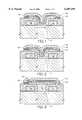
- FIG. 1is a composite cross-sectional view of a process wafer portion depicting a first embodiment of the present invention
- FIG. 2is a composite cross-sectional view of a process wafer portion depicting a second embodiment of the present invention
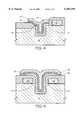
- FIG. 3is a composite cross-sectional view of a process wafer portion depicting a third embodiment of the present invention.
- FIG. 4is a composite cross-sectional view of a process wafer portion depicting a fourth embodiment of the present invention.
- FIG. 5is a composite cross-sectional view of a process wafer portion depicting a fifth embodiment of the present invention.
- the present inventionas depicted in the several embodiments of FIGS. 1-5 demonstrates process steps integrated into a fabrication process of semiconductor device, such as for a dynamic random access memory (DRAM), that will provide storage capacitor structures.
- DRAMdynamic random access memory
- the process described hereinaftermay be taken as referenced to DRAM fabrication, it is meant to serve as an example for practicing the present invention.
- the present inventionmay be integrated into any semiconductor fabrication process that requires the formation of capacitors and in particular storage capacitors.
- starting silicon substrate 10has been implanted with a conductive dopant (p-type or n-type, depending on the desired use) to form diffusion region 11.
- Diffusion region 11bridges between two neighboring control gates 12.
- control gatesare formed from parallel wordlines that are used to access a storage capacitor yet to be discussed.
- the formation of a the storage capacitor having a unique constructionis the essence of the present invention.
- TiNtitanium nitride
- MOCVDmetal organic chemical vapor deposition
- the TiN comprising layermay be any material that contains TiN.
- a suitable TiN comprising layeris a TiN x C y O z layer, where variables x, y and z range from 1 to 0. It is preferred to use a TiN comprising layer that is predominantly amorphous TiN as the amorphous TiN provides an excellent barrier to prevent the out-diffusion of conductive dopants resident in underlying layers.
- the TiN comprising layeris exposed to an oxide ambient thereby at least partially oxidizing the TiN comprising layer. The amount of the TiN layer consumed by oxidation can range from the thinnest layer of oxidation to complete oxidation which would satisfy the definition set forth of "at least partially oxidizing.”
- a layer 14 of dielectric materialis formed by methods known to those skilled in the art and preferably by chemical vapor deposition (CVD).
- CVDchemical vapor deposition
- any dielectric suitable for use as a capacitor dielectricsuch as silicon oxide (SiO 2 ) and silicon nitride (Si 3 N 4 ) it is preferred to use a dielectric material that has a dielectric constant is greater than 7.
- Suitable dielectric materialwould be a material selected from barium strontium titanate (BST), lead zirconium titanate (PZT) and lead lanthanum titanate (PLZT). If so desired the dielectric material can then be planarized.
- a top capacitor plate 15is formed from a conductive material to complete the capacitor structure of FIG. 1.
- FIG. 2As a second embodiment of the present invention and referring now to FIG. 2, the same process steps are followed to form the structure of FIG. 2 as those used to form the structure of FIG. 1, except that a conductively doped polysilicon layer 21 has been formed prior to the formation of the TiN comprising layer 13. Subsequently these two layers (21 and 13) are patterned to form the bottom capacitor plate. The structure is then completed as in FIG. 1.
- FIGS. 3-5represent the incorporation of the present invention into various capacitor processes.
- a planar capacitor making contact to a conductive plug 31is formed using the process steps described along with FIG. 1. Though both a polysilicon layer 21 and a TiN layer 13 are shown, the polysilicon layer need not be present. Also, a planar capacitor could be constructed over the diffusion region 11 as the plug 31 need not be present.
- FIG. 4depicts a trench capacitor that is formed using the process steps described along with FIG. 1. In this case only TiN layer 13 is shown, however an underlying polysilicon layer could be added so both layers would form the bottom capacitor.
- FIG. 5depicts a trench-stacked capacitor that is formed using the process steps described along with FIG. 1. Again, in this case only TiN layer 13 is shown, however an underlying polysilicon layer could be added so both layers would form the bottom capacitor.
Landscapes
- Semiconductor Memories (AREA)
Abstract
Description
Claims (25)
Priority Applications (2)
| Application Number | Priority Date | Filing Date | Title |
|---|---|---|---|
| US08/868,651US6107105A (en) | 1994-05-13 | 1997-06-04 | Amorphous tin films for an integrated capacitor dielectric/bottom plate using high dielectric constant material |
| US09/496,081US6770924B1 (en) | 1994-05-13 | 2000-02-01 | Amorphous TiN films for an integrated capacitor dielectric/bottom plate using high dielectric constant materials |
Applications Claiming Priority (2)
| Application Number | Priority Date | Filing Date | Title |
|---|---|---|---|
| US24256694A | 1994-05-13 | 1994-05-13 | |
| US08/868,651US6107105A (en) | 1994-05-13 | 1997-06-04 | Amorphous tin films for an integrated capacitor dielectric/bottom plate using high dielectric constant material |
Related Parent Applications (1)
| Application Number | Title | Priority Date | Filing Date |
|---|---|---|---|
| US24256694AContinuation | 1994-05-13 | 1994-05-13 |
Related Child Applications (1)
| Application Number | Title | Priority Date | Filing Date |
|---|---|---|---|
| US09/496,081DivisionUS6770924B1 (en) | 1994-05-13 | 2000-02-01 | Amorphous TiN films for an integrated capacitor dielectric/bottom plate using high dielectric constant materials |
Publications (1)
| Publication Number | Publication Date |
|---|---|
| US6107105Atrue US6107105A (en) | 2000-08-22 |
Family
ID=22915312
Family Applications (1)
| Application Number | Title | Priority Date | Filing Date |
|---|---|---|---|
| US08/868,651Expired - LifetimeUS6107105A (en) | 1994-05-13 | 1997-06-04 | Amorphous tin films for an integrated capacitor dielectric/bottom plate using high dielectric constant material |
Country Status (1)
| Country | Link |
|---|---|
| US (1) | US6107105A (en) |
Cited By (12)
| Publication number | Priority date | Publication date | Assignee | Title |
|---|---|---|---|---|
| US6358790B1 (en)* | 1999-01-13 | 2002-03-19 | Agere Systems Guardian Corp. | Method of making a capacitor |
| US6589867B2 (en)* | 1994-08-15 | 2003-07-08 | Micron Technology, Inc. | Method of fabricating a contact structure having a composite barrier layer between a platinum layer and a polysilicon plug |
| US20040145059A1 (en)* | 1997-10-27 | 2004-07-29 | Michio Koike | Semiconductor devices and manufacturing methods |
| US6829127B1 (en)* | 2003-03-05 | 2004-12-07 | Altera Corporation | High performance capacitor structure |
| US20080237540A1 (en)* | 2007-03-19 | 2008-10-02 | Nanosys, Inc. | Methods for encapsulating nanocrystals |
| US20100110728A1 (en)* | 2007-03-19 | 2010-05-06 | Nanosys, Inc. | Light-emitting diode (led) devices comprising nanocrystals |
| US20100155749A1 (en)* | 2007-03-19 | 2010-06-24 | Nanosys, Inc. | Light-emitting diode (led) devices comprising nanocrystals |
| US20100167011A1 (en)* | 2008-12-30 | 2010-07-01 | Nanosys, Inc. | Methods for encapsulating nanocrystals and resulting compositions |
| US9199842B2 (en) | 2008-12-30 | 2015-12-01 | Nanosys, Inc. | Quantum dot films, lighting devices, and lighting methods |
| US10214686B2 (en) | 2008-12-30 | 2019-02-26 | Nanosys, Inc. | Methods for encapsulating nanocrystals and resulting compositions |
| US11198270B2 (en) | 2008-12-30 | 2021-12-14 | Nanosys, Inc. | Quantum dot films, lighting devices, and lighting methods |
| US20220139885A1 (en)* | 2017-11-15 | 2022-05-05 | Taiwan Semiconductor Manufacturing Company, Ltd. | Integrating Passive Devices in Package Structures |
Citations (9)
| Publication number | Priority date | Publication date | Assignee | Title |
|---|---|---|---|---|
| WO1987005152A1 (en)* | 1986-02-25 | 1987-08-27 | American Telephone & Telegraph Company | Fabrication of solid-state devices having thin dielectric layers |
| US5168073A (en)* | 1991-10-31 | 1992-12-01 | Micron Technology, Inc. | Method for fabricating storage node capacitor having tungsten and etched tin storage node capacitor plate |
| US5192589A (en)* | 1991-09-05 | 1993-03-09 | Micron Technology, Inc. | Low-pressure chemical vapor deposition process for depositing thin titanium nitride films having low and stable resistivity |
| US5246881A (en)* | 1993-04-14 | 1993-09-21 | Micron Semiconductor, Inc. | Low-pressure chemical vapor deposition process for depositing high-density, highly-conformal, titanium nitride films of low bulk resistivity |
| US5279985A (en)* | 1991-09-19 | 1994-01-18 | Nec Corporation | Semiconductor device and method of fabrication thereof |
| US5335138A (en)* | 1993-02-12 | 1994-08-02 | Micron Semiconductor, Inc. | High dielectric constant capacitor and method of manufacture |
| US5466629A (en)* | 1992-07-23 | 1995-11-14 | Symetrix Corporation | Process for fabricating ferroelectric integrated circuit |
| US5489548A (en)* | 1994-08-01 | 1996-02-06 | Texas Instruments Incorporated | Method of forming high-dielectric-constant material electrodes comprising sidewall spacers |
| US5504041A (en)* | 1994-08-01 | 1996-04-02 | Texas Instruments Incorporated | Conductive exotic-nitride barrier layer for high-dielectric-constant materials |
- 1997
- 1997-06-04USUS08/868,651patent/US6107105A/ennot_activeExpired - Lifetime
Patent Citations (9)
| Publication number | Priority date | Publication date | Assignee | Title |
|---|---|---|---|---|
| WO1987005152A1 (en)* | 1986-02-25 | 1987-08-27 | American Telephone & Telegraph Company | Fabrication of solid-state devices having thin dielectric layers |
| US5192589A (en)* | 1991-09-05 | 1993-03-09 | Micron Technology, Inc. | Low-pressure chemical vapor deposition process for depositing thin titanium nitride films having low and stable resistivity |
| US5279985A (en)* | 1991-09-19 | 1994-01-18 | Nec Corporation | Semiconductor device and method of fabrication thereof |
| US5168073A (en)* | 1991-10-31 | 1992-12-01 | Micron Technology, Inc. | Method for fabricating storage node capacitor having tungsten and etched tin storage node capacitor plate |
| US5466629A (en)* | 1992-07-23 | 1995-11-14 | Symetrix Corporation | Process for fabricating ferroelectric integrated circuit |
| US5335138A (en)* | 1993-02-12 | 1994-08-02 | Micron Semiconductor, Inc. | High dielectric constant capacitor and method of manufacture |
| US5246881A (en)* | 1993-04-14 | 1993-09-21 | Micron Semiconductor, Inc. | Low-pressure chemical vapor deposition process for depositing high-density, highly-conformal, titanium nitride films of low bulk resistivity |
| US5489548A (en)* | 1994-08-01 | 1996-02-06 | Texas Instruments Incorporated | Method of forming high-dielectric-constant material electrodes comprising sidewall spacers |
| US5504041A (en)* | 1994-08-01 | 1996-04-02 | Texas Instruments Incorporated | Conductive exotic-nitride barrier layer for high-dielectric-constant materials |
Cited By (27)
| Publication number | Priority date | Publication date | Assignee | Title |
|---|---|---|---|---|
| US6589867B2 (en)* | 1994-08-15 | 2003-07-08 | Micron Technology, Inc. | Method of fabricating a contact structure having a composite barrier layer between a platinum layer and a polysilicon plug |
| US6930039B2 (en) | 1994-08-15 | 2005-08-16 | Micron Technology, Inc. | Method of fabricating a contact structure having a composite barrier layer between a platinum layer and a polysilicon plug |
| US20040145059A1 (en)* | 1997-10-27 | 2004-07-29 | Michio Koike | Semiconductor devices and manufacturing methods |
| US6979612B2 (en)* | 1997-10-27 | 2005-12-27 | Seiko Epson Corp. | Semiconductor devices and manufacturing methods |
| US6358790B1 (en)* | 1999-01-13 | 2002-03-19 | Agere Systems Guardian Corp. | Method of making a capacitor |
| US6829127B1 (en)* | 2003-03-05 | 2004-12-07 | Altera Corporation | High performance capacitor structure |
| US20080237540A1 (en)* | 2007-03-19 | 2008-10-02 | Nanosys, Inc. | Methods for encapsulating nanocrystals |
| US20100110728A1 (en)* | 2007-03-19 | 2010-05-06 | Nanosys, Inc. | Light-emitting diode (led) devices comprising nanocrystals |
| US20100155749A1 (en)* | 2007-03-19 | 2010-06-24 | Nanosys, Inc. | Light-emitting diode (led) devices comprising nanocrystals |
| US9909062B2 (en) | 2007-03-19 | 2018-03-06 | Nanosys, Inc. | Light-emitting diode (LED) devices comprising nanocrystals |
| US9677001B2 (en) | 2007-03-19 | 2017-06-13 | Nanosys, Inc. | Light-emitting diode (LED) devices comprising nanocrystals |
| US9139767B2 (en) | 2008-12-30 | 2015-09-22 | Nanosys, Inc. | Methods for encapsulating nanocrystals and resulting compositions |
| US10302845B2 (en) | 2008-12-30 | 2019-05-28 | Nanosys, Inc. | Quantum dot films, lighting devices, and lighting methods |
| US9199842B2 (en) | 2008-12-30 | 2015-12-01 | Nanosys, Inc. | Quantum dot films, lighting devices, and lighting methods |
| US8343575B2 (en) | 2008-12-30 | 2013-01-01 | Nanosys, Inc. | Methods for encapsulating nanocrystals and resulting compositions |
| US9804319B2 (en) | 2008-12-30 | 2017-10-31 | Nanosys, Inc. | Quantum dot films, lighting devices, and lighting methods |
| US20100167011A1 (en)* | 2008-12-30 | 2010-07-01 | Nanosys, Inc. | Methods for encapsulating nanocrystals and resulting compositions |
| US10214686B2 (en) | 2008-12-30 | 2019-02-26 | Nanosys, Inc. | Methods for encapsulating nanocrystals and resulting compositions |
| US8697471B2 (en) | 2008-12-30 | 2014-04-15 | Nanosys, Inc. | Methods for encapsulating nanocrystals and resulting compositions |
| US10444423B2 (en) | 2008-12-30 | 2019-10-15 | Nanosys, Inc. | Quantum dot films, lighting devices, and lighting methods |
| US10544362B2 (en) | 2008-12-30 | 2020-01-28 | Nanosys, Inc. | Methods for encapsulating nanocrystals and resulting compositions |
| US10899105B2 (en) | 2008-12-30 | 2021-01-26 | Nanosys, Inc. | Quantum dot films, lighting devices, and lighting methods |
| US11198270B2 (en) | 2008-12-30 | 2021-12-14 | Nanosys, Inc. | Quantum dot films, lighting devices, and lighting methods |
| US11420412B2 (en) | 2008-12-30 | 2022-08-23 | Nanosys, Inc. | Quantum dot films, lighting devices, and lighting methods |
| US11396158B2 (en) | 2008-12-30 | 2022-07-26 | Nanosys, Inc. | Quantum dot films, lighting devices, and lighting methods |
| US20220139885A1 (en)* | 2017-11-15 | 2022-05-05 | Taiwan Semiconductor Manufacturing Company, Ltd. | Integrating Passive Devices in Package Structures |
| US12132029B2 (en)* | 2017-11-15 | 2024-10-29 | Taiwan Semiconductor Manufacturing Company, Ltd. | Integrating passive devices in package structures |
Similar Documents
| Publication | Publication Date | Title |
|---|---|---|
| US6399459B2 (en) | Double layer electrode and barrier system on hemispherical grain silicon for use with high dielectric constant materials and methods for fabricating the same | |
| US7005695B1 (en) | Integrated circuitry including a capacitor with an amorphous and a crystalline high K capacitor dielectric region | |
| US7157783B2 (en) | Platinum stuffed with silicon oxide as a diffusion oxygen barrier for semiconductor devices | |
| US5436477A (en) | Semiconductor memory device with high dielectric capacitor structure | |
| US5618746A (en) | Method for manufacturing a capacitor of semiconductor device having diffusion-blocking films | |
| US6791131B1 (en) | Method for forming a storage cell capacitor compatible with high dielectric constant materials | |
| US5905278A (en) | Semiconductor device having a dielectric film and a fabrication process thereof | |
| US5953619A (en) | Semiconductor device with perovskite capacitor and its manufacture method | |
| JP2929436B2 (en) | Semiconductor memory device and method of manufacturing the same | |
| US5742472A (en) | Stacked capacitors for integrated circuit devices and related methods | |
| US6107105A (en) | Amorphous tin films for an integrated capacitor dielectric/bottom plate using high dielectric constant material | |
| US6888189B2 (en) | Dielectric element including oxide-based dielectric film and method of fabricating the same | |
| US6218258B1 (en) | Method for fabricating semiconductor device including capacitor with improved bottom electrode | |
| US6228701B1 (en) | Apparatus and method for minimizing diffusion in stacked capacitors formed on silicon plugs | |
| US6136659A (en) | Production process for a capacitor electrode formed of a platinum metal | |
| US6503792B2 (en) | Method for fabricating a patterned metal-oxide-containing layer | |
| US6417101B2 (en) | Method for manufacturing semiconductor memory device incorporating therein copacitor | |
| US6762476B2 (en) | Dielectric element including oxide dielectric film and method of manufacturing the same | |
| KR100219506B1 (en) | Capacitor Manufacturing Method of Semiconductor Device | |
| US6770924B1 (en) | Amorphous TiN films for an integrated capacitor dielectric/bottom plate using high dielectric constant materials | |
| US20010027004A1 (en) | Semiconductor device having capacitor and method of manufacturing the same | |
| US6946340B2 (en) | Method of fabricating ferroelectric memory device with photoresist and capping layer | |
| US6465300B2 (en) | Method for forming a lower electrode for use in a semiconductor device | |
| KR100234393B1 (en) | Ferroelectric capacitor of semiconductor device and manufacturing method thereof | |
| KR20000036201A (en) | Process for producing barrier-free semiconductor storage assemblies |
Legal Events
| Date | Code | Title | Description |
|---|---|---|---|
| STCF | Information on status: patent grant | Free format text:PATENTED CASE | |
| FPAY | Fee payment | Year of fee payment:4 | |
| FPAY | Fee payment | Year of fee payment:8 | |
| FPAY | Fee payment | Year of fee payment:12 | |
| AS | Assignment | Owner name:U.S. BANK NATIONAL ASSOCIATION, AS COLLATERAL AGENT, CALIFORNIA Free format text:SECURITY INTEREST;ASSIGNOR:MICRON TECHNOLOGY, INC.;REEL/FRAME:038669/0001 Effective date:20160426 Owner name:U.S. BANK NATIONAL ASSOCIATION, AS COLLATERAL AGEN Free format text:SECURITY INTEREST;ASSIGNOR:MICRON TECHNOLOGY, INC.;REEL/FRAME:038669/0001 Effective date:20160426 | |
| AS | Assignment | Owner name:MORGAN STANLEY SENIOR FUNDING, INC., AS COLLATERAL AGENT, MARYLAND Free format text:PATENT SECURITY AGREEMENT;ASSIGNOR:MICRON TECHNOLOGY, INC.;REEL/FRAME:038954/0001 Effective date:20160426 Owner name:MORGAN STANLEY SENIOR FUNDING, INC., AS COLLATERAL Free format text:PATENT SECURITY AGREEMENT;ASSIGNOR:MICRON TECHNOLOGY, INC.;REEL/FRAME:038954/0001 Effective date:20160426 | |
| AS | Assignment | Owner name:U.S. BANK NATIONAL ASSOCIATION, AS COLLATERAL AGENT, CALIFORNIA Free format text:CORRECTIVE ASSIGNMENT TO CORRECT THE REPLACE ERRONEOUSLY FILED PATENT #7358718 WITH THE CORRECT PATENT #7358178 PREVIOUSLY RECORDED ON REEL 038669 FRAME 0001. ASSIGNOR(S) HEREBY CONFIRMS THE SECURITY INTEREST;ASSIGNOR:MICRON TECHNOLOGY, INC.;REEL/FRAME:043079/0001 Effective date:20160426 Owner name:U.S. BANK NATIONAL ASSOCIATION, AS COLLATERAL AGEN Free format text:CORRECTIVE ASSIGNMENT TO CORRECT THE REPLACE ERRONEOUSLY FILED PATENT #7358718 WITH THE CORRECT PATENT #7358178 PREVIOUSLY RECORDED ON REEL 038669 FRAME 0001. ASSIGNOR(S) HEREBY CONFIRMS THE SECURITY INTEREST;ASSIGNOR:MICRON TECHNOLOGY, INC.;REEL/FRAME:043079/0001 Effective date:20160426 | |
| AS | Assignment | Owner name:MICRON TECHNOLOGY, INC., IDAHO Free format text:RELEASE BY SECURED PARTY;ASSIGNOR:U.S. BANK NATIONAL ASSOCIATION, AS COLLATERAL AGENT;REEL/FRAME:047243/0001 Effective date:20180629 | |
| AS | Assignment | Owner name:MICRON TECHNOLOGY, INC., IDAHO Free format text:RELEASE BY SECURED PARTY;ASSIGNOR:MORGAN STANLEY SENIOR FUNDING, INC., AS COLLATERAL AGENT;REEL/FRAME:050937/0001 Effective date:20190731 |