US6104280A - Method of manufacturing and testing an electronic device, and an electronic device - Google Patents
Method of manufacturing and testing an electronic device, and an electronic deviceDownload PDFInfo
- Publication number
- US6104280A US6104280AUS08/954,551US95455197AUS6104280AUS 6104280 AUS6104280 AUS 6104280AUS 95455197 AUS95455197 AUS 95455197AUS 6104280 AUS6104280 AUS 6104280A
- Authority
- US
- United States
- Prior art keywords
- substrate
- battery
- coupled
- circuit
- conductive
- Prior art date
- Legal status (The legal status is an assumption and is not a legal conclusion. Google has not performed a legal analysis and makes no representation as to the accuracy of the status listed.)
- Expired - Lifetime
Links
- 238000004519manufacturing processMethods0.000titleabstractdescription13
- 238000010998test methodMethods0.000titleabstractdescription3
- 239000000758substrateSubstances0.000claimsabstractdescription59
- 239000004593EpoxySubstances0.000claimsabstractdescription54
- 230000008878couplingEffects0.000claimsabstractdescription12
- 238000010168coupling processMethods0.000claimsabstractdescription12
- 238000005859coupling reactionMethods0.000claimsabstractdescription12
- 239000004020conductorSubstances0.000claimsdescription9
- 229920006267polyester filmPolymers0.000claimsdescription4
- 239000002184metalSubstances0.000claimsdescription3
- 229910052751metalInorganic materials0.000claimsdescription3
- 229920002457flexible plasticPolymers0.000claims1
- 239000002985plastic filmSubstances0.000claims1
- 238000012360testing methodMethods0.000abstractdescription22
- 238000000034methodMethods0.000abstractdescription6
- 238000012545processingMethods0.000description7
- RYGMFSIKBFXOCR-UHFFFAOYSA-NCopperChemical compound[Cu]RYGMFSIKBFXOCR-UHFFFAOYSA-N0.000description5
- 229910052802copperInorganic materials0.000description5
- 239000010949copperSubstances0.000description5
- 239000000463materialSubstances0.000description5
- 239000003990capacitorSubstances0.000description4
- 238000004891communicationMethods0.000description3
- 230000005540biological transmissionEffects0.000description2
- 238000010276constructionMethods0.000description2
- 239000007788liquidSubstances0.000description2
- 229910052709silverInorganic materials0.000description2
- 239000004332silverSubstances0.000description2
- 230000003319supportive effectEffects0.000description2
- 230000009977dual effectEffects0.000description1
- 230000000694effectsEffects0.000description1
- 230000006870functionEffects0.000description1
- 238000004377microelectronicMethods0.000description1
- 238000012986modificationMethods0.000description1
- 230000004048modificationEffects0.000description1
- 238000012544monitoring processMethods0.000description1
- 238000004806packaging method and processMethods0.000description1
- 229920000642polymerPolymers0.000description1
- 238000011160researchMethods0.000description1
- 238000007650screen-printingMethods0.000description1
- 239000002356single layerSubstances0.000description1
Images


Classifications
- H—ELECTRICITY
- H05—ELECTRIC TECHNIQUES NOT OTHERWISE PROVIDED FOR
- H05K—PRINTED CIRCUITS; CASINGS OR CONSTRUCTIONAL DETAILS OF ELECTRIC APPARATUS; MANUFACTURE OF ASSEMBLAGES OF ELECTRICAL COMPONENTS
- H05K1/00—Printed circuits
- H05K1/02—Details
- H05K1/0286—Programmable, customizable or modifiable circuits
- H05K1/0293—Individual printed conductors which are adapted for modification, e.g. fusable or breakable conductors, printed switches
- G—PHYSICS
- G01—MEASURING; TESTING
- G01R—MEASURING ELECTRIC VARIABLES; MEASURING MAGNETIC VARIABLES
- G01R31/00—Arrangements for testing electric properties; Arrangements for locating electric faults; Arrangements for electrical testing characterised by what is being tested not provided for elsewhere
- G01R31/50—Testing of electric apparatus, lines, cables or components for short-circuits, continuity, leakage current or incorrect line connections
- G01R31/66—Testing of connections, e.g. of plugs or non-disconnectable joints
- G01R31/70—Testing of connections between components and printed circuit boards
- H—ELECTRICITY
- H05—ELECTRIC TECHNIQUES NOT OTHERWISE PROVIDED FOR
- H05K—PRINTED CIRCUITS; CASINGS OR CONSTRUCTIONAL DETAILS OF ELECTRIC APPARATUS; MANUFACTURE OF ASSEMBLAGES OF ELECTRICAL COMPONENTS
- H05K1/00—Printed circuits
- H05K1/02—Details
- H05K1/0266—Marks, test patterns or identification means
- H05K1/0268—Marks, test patterns or identification means for electrical inspection or testing
- H—ELECTRICITY
- H05—ELECTRIC TECHNIQUES NOT OTHERWISE PROVIDED FOR
- H05K—PRINTED CIRCUITS; CASINGS OR CONSTRUCTIONAL DETAILS OF ELECTRIC APPARATUS; MANUFACTURE OF ASSEMBLAGES OF ELECTRICAL COMPONENTS
- H05K2201/00—Indexing scheme relating to printed circuits covered by H05K1/00
- H05K2201/10—Details of components or other objects attached to or integrated in a printed circuit board
- H05K2201/10007—Types of components
- H05K2201/10037—Printed or non-printed battery
- H—ELECTRICITY
- H05—ELECTRIC TECHNIQUES NOT OTHERWISE PROVIDED FOR
- H05K—PRINTED CIRCUITS; CASINGS OR CONSTRUCTIONAL DETAILS OF ELECTRIC APPARATUS; MANUFACTURE OF ASSEMBLAGES OF ELECTRICAL COMPONENTS
- H05K2203/00—Indexing scheme relating to apparatus or processes for manufacturing printed circuits covered by H05K3/00
- H05K2203/17—Post-manufacturing processes
- H05K2203/173—Adding connections between adjacent pads or conductors, e.g. for modifying or repairing
- H—ELECTRICITY
- H05—ELECTRIC TECHNIQUES NOT OTHERWISE PROVIDED FOR
- H05K—PRINTED CIRCUITS; CASINGS OR CONSTRUCTIONAL DETAILS OF ELECTRIC APPARATUS; MANUFACTURE OF ASSEMBLAGES OF ELECTRICAL COMPONENTS
- H05K3/00—Apparatus or processes for manufacturing printed circuits
- H05K3/30—Assembling printed circuits with electric components, e.g. with resistor
- H05K3/32—Assembling printed circuits with electric components, e.g. with resistor electrically connecting electric components or wires to printed circuits
- H05K3/321—Assembling printed circuits with electric components, e.g. with resistor electrically connecting electric components or wires to printed circuits by conductive adhesives
- Y—GENERAL TAGGING OF NEW TECHNOLOGICAL DEVELOPMENTS; GENERAL TAGGING OF CROSS-SECTIONAL TECHNOLOGIES SPANNING OVER SEVERAL SECTIONS OF THE IPC; TECHNICAL SUBJECTS COVERED BY FORMER USPC CROSS-REFERENCE ART COLLECTIONS [XRACs] AND DIGESTS
- Y10—TECHNICAL SUBJECTS COVERED BY FORMER USPC
- Y10T—TECHNICAL SUBJECTS COVERED BY FORMER US CLASSIFICATION
- Y10T29/00—Metal working
- Y10T29/49—Method of mechanical manufacture
- Y10T29/49002—Electrical device making
- Y10T29/49004—Electrical device making including measuring or testing of device or component part
- Y—GENERAL TAGGING OF NEW TECHNOLOGICAL DEVELOPMENTS; GENERAL TAGGING OF CROSS-SECTIONAL TECHNOLOGIES SPANNING OVER SEVERAL SECTIONS OF THE IPC; TECHNICAL SUBJECTS COVERED BY FORMER USPC CROSS-REFERENCE ART COLLECTIONS [XRACs] AND DIGESTS
- Y10—TECHNICAL SUBJECTS COVERED BY FORMER USPC
- Y10T—TECHNICAL SUBJECTS COVERED BY FORMER US CLASSIFICATION
- Y10T29/00—Metal working
- Y10T29/49—Method of mechanical manufacture
- Y10T29/49002—Electrical device making
- Y10T29/49108—Electric battery cell making
- Y10T29/49115—Electric battery cell making including coating or impregnating
- Y—GENERAL TAGGING OF NEW TECHNOLOGICAL DEVELOPMENTS; GENERAL TAGGING OF CROSS-SECTIONAL TECHNOLOGIES SPANNING OVER SEVERAL SECTIONS OF THE IPC; TECHNICAL SUBJECTS COVERED BY FORMER USPC CROSS-REFERENCE ART COLLECTIONS [XRACs] AND DIGESTS
- Y10—TECHNICAL SUBJECTS COVERED BY FORMER USPC
- Y10T—TECHNICAL SUBJECTS COVERED BY FORMER US CLASSIFICATION
- Y10T29/00—Metal working
- Y10T29/49—Method of mechanical manufacture
- Y10T29/49002—Electrical device making
- Y10T29/49117—Conductor or circuit manufacturing
- Y10T29/49124—On flat or curved insulated base, e.g., printed circuit, etc.
- Y10T29/4913—Assembling to base an electrical component, e.g., capacitor, etc.
- Y—GENERAL TAGGING OF NEW TECHNOLOGICAL DEVELOPMENTS; GENERAL TAGGING OF CROSS-SECTIONAL TECHNOLOGIES SPANNING OVER SEVERAL SECTIONS OF THE IPC; TECHNICAL SUBJECTS COVERED BY FORMER USPC CROSS-REFERENCE ART COLLECTIONS [XRACs] AND DIGESTS
- Y10—TECHNICAL SUBJECTS COVERED BY FORMER USPC
- Y10T—TECHNICAL SUBJECTS COVERED BY FORMER US CLASSIFICATION
- Y10T29/00—Metal working
- Y10T29/49—Method of mechanical manufacture
- Y10T29/49002—Electrical device making
- Y10T29/49117—Conductor or circuit manufacturing
- Y10T29/49124—On flat or curved insulated base, e.g., printed circuit, etc.
- Y10T29/49155—Manufacturing circuit on or in base
Definitions
- This inventionrelates to techniques for manufacturing circuitry.
- the inventionalso relates to methods of testing circuitry.
- circuitryWhen manufacturing circuitry, after attaching components to a substrate, such as to a circuit board or flexible material, it is desirable to perform testing. These tests, among other things, are to make sure that circuit connections have been properly made, are sufficiently conductive, and are not cold connections. Such testing is known in the art as "in circuit” testing. It is difficult to perform such testing while power is supplied to the circuitry, such as by an on board cell or battery.
- circuit testingis performed for a wide variety of types of circuitry.
- circuitry for which in circuit testing is performedis in identification circuitry.
- Some such systemsgenerally include an identification device including circuitry provided with a unique identification code in order to distinguish between a number of different devices.
- the identification devicesare entirely passive (have no power supply).
- this identification systemis only capable of operation over a relatively short range, limited by the size of a magnetic field used to supply power to the devices and to communicate with the devices.
- the systemincludes an active transponder device affixed to an object to be monitored which receives a signal from an interrogator. The device receives the signal, then generates and transmits a responsive signal. Because active devices have their own power sources, they do not need to be in close proximity to an interrogator or reader to receive power via magnetic coupling. Therefore, active transponder devices tend to be more suitable for applications requiring tracking of a tagged device that may not be in close proximity to an interrogator. For example, active transponder devices tend to be more suitable for inventory control or tracking.
- Electronic identification systemscan also be used for remote payment.
- the toll boothcan determine the identity of the radio frequency identification device, and thus of the owner of the device, and debit an account held by the owner for payment of toll or can receive a credit card number against which the toll can be charged.
- remote paymentis possible for a variety of other goods or services.
- the inventionprovides a method of manufacturing and testing an electronic circuit.
- a plurality of conductive tracesare formed on a substrate and a gap is provided in one of the conductive traces.
- a circuit componentis attached to the substrate and coupled to at least one of the conductive traces.
- a batteryis supported on the substrate and coupled to at least one of the conductive traces, wherein a completed circuit would be defined, including the traces, circuit component, and battery, but for the gap. Electrical connections are verified by performing an in circuit test, after the circuit component is attached and the battery is supported.
- a jumperis employed to electrically close the gap, and complete the circuit, after the electrical connections are verified.
- employing the jumpercomprises employing conductive epoxy.
- employing a jumpercomprises placing a conductor across the gap and coupling the conductor to traces on either side of the gap with conductive epoxy.
- employing a jumpercomprises placing a resistor across the gap and coupling the resistor to traces on either side of the gap with conductive epoxy.
- a jumperis formed by wire bonding; e.g., by ultrasonically bonding a wire loop to traces on either side of the gap.
- the batteryis mechanically supported from the substrate by epoxy. In another aspect of the invention, the battery is electrically coupled to at least one of the traces by conductive epoxy.
- Another aspect of the inventionprovides an electronic circuit comprising a substrate, and a plurality of conductive traces on the substrate, with a gap in one of the conductive traces.
- a circuit componentis attached to the substrate and coupled to at least one of the conductive traces.
- a batteryis supported on the substrate and coupled to at least one of the conductive traces, wherein a completed circuit would be defined, including the traces, circuit component, and battery, but for the gap.
- a jumperelectrically closes the gap and completes the circuit.
- the jumpercomprises conductive epoxy.
- the jumpercomprises conductive epoxy having a resistance of less than 1000 ohms prior to curing.
- the jumpercomprises a conductor across the gap and the conductive epoxy couples the conductor to the conductive traces on either side of the gap.
- the jumpercomprises a resistor across the gap and the conductive epoxy couples the resistor to the conductive traces on either side of the gap.
- the size of the gapis approximately 30 thousandths of an inch.
- the circuit componentcomprises an integrated circuit.
- the circuit componentcomprises an integrated circuit defining a wireless identification device including a receiver, a transponder, a microprocessor, and a memory.
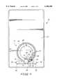
- FIG. 1is a plan view showing construction details of an electronic device embodying the invention prior to completing or closing a housing thereof.
- FIG. 2is a plan view of a substrate employed in a method of manufacturing the device of FIG. 1.
- FIG. 3is a plan view of the substrate of FIG. 2 after further processing in accordance with the method of manufacturing the device of FIG. 1.
- FIG. 4is a plan view showing further processing in accordance with the method of manufacturing the device of FIG. 1.
- FIG. 5is a plan view showing further processing in accordance with the method of manufacturing the device of FIG. 1.
- FIG. 6is a plan view showing further processing in accordance with the method of manufacturing the device of FIG. 1.
- FIG. 7is a plan view illustrating an alternative embodiment of the invention at a processing stage similar to the stage illustrated in FIG. 6.
- FIG. 8is a plan view illustrating another alternative embodiment of the invention at a processing stage similar to the stage illustrated in FIG. 6.
- FIG. 9is a plan view illustrating processing after the stage shown in FIG. 6, 7, or 8.
- FIG. 1illustrates an electronic device 10 in accordance with one embodiment of the invention.
- the device 10includes a substrate 12.
- the substrate 12can be a printed circuit board or a substrate appropriate for a flex circuit.
- the device 10further includes circuitry 14 including circuit components 16 on the substrate.
- the inventionhas application to circuitry including any of various types of circuit components.
- the circuit components 16can include one or more integrated circuits.
- the circuit components 16include an integrated circuit 18 as described in U.S. patent application Ser. No. 08/705,043, filed Aug. 29, 1996 and incorporated herein by reference.
- the integrated circuit 18comprises a receiver, a transmitter or backscatter modulator, a microprocessor, and a memory, and is useful for inventory monitoring or RFID (radio frequency identification device) or RIC (remote intelligent communications) applications.
- the circuit components 16further include a capacitor 20.
- Other types of circuit componentssuch as different types of integrated circuits, resistors, capacitors, inductors, etc. are employed in alternative embodiments.
- the circuitry 14further includes conductors or circuit traces 22 on the substrate 12 connecting together the circuit components 16.
- the circuit traces 22are typically copper if the substrate 12 is a printed circuit board, and are typically copper or Printed Thick Film (PTF) in a flex circuit.
- Printed Thick Filmcomprises a polymer filled with flecks of metal such as silver or copper.
- the circuitry 14includes a first or negative battery connection or terminal 23 (see FIG. 3).
- the negative battery connection 23is defined by a plurality of radially spaced apart contact points which provide an enhanced connection. In alternative embodiments a single, contiguous, or central contact point is provided. Other forms of battery connections, such as metal clip connections can be employed.
- the circuitry 14further includes a second or positive battery connection or terminal 25 defined by the conductive traces.
- the circuit traces 22connect at least one antenna to the integrated circuit 18 for electromagnetic transmission and reception. More particularly, in the illustrated embodiment, the integrated circuit 18 receives and sends microwave frequencies, and one of the circuit traces 22 defines a loop antenna 24 appropriately sized to receive microwave transmissions of a selected frequency, and other traces 22 define a dipole antenna 26 appropriately sized for responding at a selected microwave frequency, such as by backscatter reflection.
- the device 10further includes a power source 28.
- the power source 28is a battery.
- the batteryis a thin profile or button-type cell forming a small, thin energy cell more commonly utilized in watches and small electronic devices requiring a thin profile.
- Such battery cellshave a pair of terminals or electrodes: a lid or negative terminal, and a can or positive terminal.
- multiple batteriesare provided (e.g., coupled together in series or parallel).
- the device 10can be included in any appropriate housing or packaging. Various methods of manufacturing housings are described in commonly assigned U.S. Pat. No. 5,988,510, issued Nov. 23, 1999, and incorporated herein by reference. In the illustrated embodiment, the device 10 includes a housing defined in part by the substrate.
- FIGS. 2-9A method of manufacturing the device 10 will now be described, reference being made to FIGS. 2-9.
- the substrate 12is provided.
- substraterefers to any supporting or supportive structure, including, but not limited to, a supportive single layer of material or multiple layer constructions.
- the substrate 12comprises a polyester film. Other materials are possible.
- the substratecan be a printed circuit board.
- the circuit traces 22are then defined, as shown in FIG. 3.
- the circuit traces 22are typically copper if the substrate 12 is a printed circuit board, and are typically copper or Printed Thick Film (PTF) in a flex circuit.
- PTFis formed or applied over the substrate 12 to define the circuit traces 22.
- the circuit traces 22interconnect the circuit components 16.
- the circuit traces 22define, among other things, the first or negative battery connection 23 and the second or positive battery connection 25.
- One manner of forming or applying the conductive ink on the substrateis to screen print the ink on the substrate through conventional screen printing techniques.
- a gap 30is provided along a trace 22 or spaced apart portions are defined in the traces which cause an open circuit unless they are electrically coupled together. After the battery and integrated circuit are coupled to the traces 22, a complete circuit would be formed, including the circuit traces, the integrated circuit 16 (see FIG. 1), and the battery, but for the gap.
- the size of the gapis approximately 30 mils (thousandths of an inch). In one embodiment, the size of the gap is 30 mils or less. In another embodiment, the size of the gap is between 10 and 50 mils. In a more particular embodiment, the size of the gap is between 20 and 40 mils. In another embodiment, the size of the gap is sufficiently small that it can be bridged by a drop of conductive epoxy.
- Conductive epoxy 32is applied over desired areas (e.g., under the battery, under the integrated circuit, etc.) using a stencil printer to assist in material application, as shown in FIG. 4.
- the conductive epoxyis used to assist in component attachment.
- the battery 28is provided and mounted on the substrate 12 using the conductive epoxy on the connection 23 to secure the battery 28 to the substrate 12, as shown in FIG. 5.
- the battery 28is placed lid down such that the conductive epoxy makes electrical contact between the negative terminal of the battery and at least a portion of the first battery connection 23 that extends underneath the lid of the battery in the view shown in FIG. 1.
- Conductive epoxyis dispensed relative to the battery perimetral edge using a syringe dispenser, after the battery 28 is mounted.
- the conductive epoxyelectrically connects the perimetral edge of the battery 28 with an adjacent arcuate portion of the second battery connection 25.
- the perimetral edgedefines the can of the battery, such that the conductive epoxy connects the positive terminal of the battery to the battery connection terminal 25.
- the integrated circuit 18is provided and mounted on the substrate 12 using the conductive epoxy (e.g., picked and placed using surface mounting techniques), to produce the device shown in FIG. 6.
- conductive epoxye.g., picked and placed using surface mounting techniques
- An exemplary and preferred integrated circuitryis described in U.S. patent application Ser. No. 08/705,043 incorporated by reference above.
- the integrated circuit 18has pins, and the pins are coupled to appropriate conductive traces (e.g., using conductive epoxy) for connection of the integrated circuit 18 to the battery 28. If the integrated circuit 18 is used for communications, as is the case for the illustrated embodiment, pins of the integrated circuit 18 are coupled to conductive traces 22 defining one or more antennas 24 and 26.
- the integrated circuit 18defines a wireless identification device including a receiver, a modulator, a microprocessor and a memory.
- the receiverreceives microwave frequencies and the modulator is a backscatter modulator.
- the capacitor 20is similarly provided and mounted.
- the integrated circuit 18, capacitor 20 and battery 28can be provided and mounted to the substrate 12 in any order, or can occur simultaneously.
- a jumper 34is employed to electrically close or repair the gap 30 (see FIG. 3) and complete the circuit defined by the circuitry 14, shown in FIG. 1.
- a jumper 34comprises employing conductive epoxy 36.
- employing a jumper 34comprises dispensing conductive epoxy 36 over the gap 30.
- employing a jumper 34comprises dispensing conductive epoxy having a resistance of less than 1000 ohms within, for example, 500 milliseconds (or less) of being dispensed.
- the conductive epoxyhas a resistance of less than 1000 ohms within 200 milliseconds of being dispensed.
- One exemplary conductive epoxy that could by usedis Quick Connect Silver, EXPFDA-4118-D/4107 produced by International Micro Electronics Research Corporation, 8010 Dearborne Rd., Nampa, Id. 83686. This is in contrast to the conductive epoxy used to connect the battery 28 to the circuit traces 22.
- the conductive epoxy 32 used to connect the battery to the circuit traces 22is typically isotropic conductive epoxy that has a low and unstable conductivity until partially cured. This epoxy 22 performs s dual functions of forming electrical connections and mechanically supporting the battery 28 from the substrate 12. If the gap 30 is not employed, this slow curing may not allow the circuitry 14 to power up properly. For example, the integrated circuit 18 may lock up.
- the battery 28was not connected until the in circuit testing was completed. Then, the battery 28 was connected and another in circuit test would have to be performed to test the battery connections. Also, a reboot of the circuitry 14 had to be performed because conductive epoxy used to connect the battery 28 to the integrated circuit 18 does not have an uncured conductivity that is sufficiently high. Provision of the gap 30 and a sufficiently conductive material solves all these problems.
- employing a jumper 34comprises placing a conductor 38 across the gap 30 and coupling the conductor 38 to traces 40 and 42 on either side of the gap 30 with conductive epoxy 43 (e.g., conductive epoxy having a resistance of less than 1000 ohms within 500 milliseconds of being dispensed) or by wire bonding (ultrasonic bonding).
- conductive epoxy 43e.g., conductive epoxy having a resistance of less than 1000 ohms within 500 milliseconds of being dispensed
- employing a jumper 34comprises placing a resistor 44 across the gap 30 and coupling the resistor to traces on either side of the gap 30 with conductive liquid such as conductive epoxy (e.g., conductive epoxy having a resistance of less than 1000 ohms within 500 milliseconds of being dispensed).
- the gap 30would typically be larger than 30 mils and may be, for example, a distance less than or approximating the length of a resistor.
- the conductive epoxyis then cured.
- encapsulating epoxy material 46is flowed or provided to encapsulate the substrate 12, to cover the integrated circuit 18, battery 28, and conductive traces 22 and to define a second housing portion.
- the inventionallows in circuit testing to be performed after a battery has been electrically and mechanically coupled using conductive epoxy.
- Two step in circuit testing, before and after inserting a battery,is avoided.
- In circuit testingcan be performed after the battery is supported from the housing by conductive epoxy.
- Lock up of circuitryis avoided because connecting the battery to the circuitry now involves using only a small amount of conductive epoxy, that does not need to mechanically support the battery from the housing.
- Conductive epoxy used to mechanically support the battery from the housing and to electrically connect the battery to circuit tracesis allowed to cure before the gap is closed with conductive epoxy. The connection made between the battery and the circuit traces, with conductive epoxy, can also be tested during the in circuit test.
Landscapes
- Engineering & Computer Science (AREA)
- Microelectronics & Electronic Packaging (AREA)
- Physics & Mathematics (AREA)
- General Physics & Mathematics (AREA)
- Parts Printed On Printed Circuit Boards (AREA)
- Structure Of Printed Boards (AREA)
Abstract
Description
Claims (6)
Priority Applications (5)
| Application Number | Priority Date | Filing Date | Title |
|---|---|---|---|
| US08/954,551US6104280A (en) | 1997-10-20 | 1997-10-20 | Method of manufacturing and testing an electronic device, and an electronic device |
| US09/392,068US6167614B1 (en) | 1997-10-20 | 1999-09-08 | Method of manufacturing and testing an electronic device, and an electronic device |
| US09/393,224US6211785B1 (en) | 1997-10-20 | 1999-09-09 | Method of manufacturing and testing an electronic device, and an electronic device |
| US09/617,636US6344792B1 (en) | 1997-10-20 | 2000-07-17 | Method of manufacturing and testing an electronic device, and a electronic device |
| US09/767,593US6359561B2 (en) | 1997-10-20 | 2001-01-22 | Method of manufacturing and testing an electronic device, and an electronic device |
Applications Claiming Priority (1)
| Application Number | Priority Date | Filing Date | Title |
|---|---|---|---|
| US08/954,551US6104280A (en) | 1997-10-20 | 1997-10-20 | Method of manufacturing and testing an electronic device, and an electronic device |
Related Child Applications (3)
| Application Number | Title | Priority Date | Filing Date |
|---|---|---|---|
| US09/392,068DivisionUS6167614B1 (en) | 1997-10-20 | 1999-09-08 | Method of manufacturing and testing an electronic device, and an electronic device |
| US09/393,224DivisionUS6211785B1 (en) | 1997-10-20 | 1999-09-09 | Method of manufacturing and testing an electronic device, and an electronic device |
| US09/617,636ContinuationUS6344792B1 (en) | 1997-10-20 | 2000-07-17 | Method of manufacturing and testing an electronic device, and a electronic device |
Publications (1)
| Publication Number | Publication Date |
|---|---|
| US6104280Atrue US6104280A (en) | 2000-08-15 |
Family
ID=25495599
Family Applications (5)
| Application Number | Title | Priority Date | Filing Date |
|---|---|---|---|
| US08/954,551Expired - LifetimeUS6104280A (en) | 1997-10-20 | 1997-10-20 | Method of manufacturing and testing an electronic device, and an electronic device |
| US09/392,068Expired - LifetimeUS6167614B1 (en) | 1997-10-20 | 1999-09-08 | Method of manufacturing and testing an electronic device, and an electronic device |
| US09/393,224Expired - LifetimeUS6211785B1 (en) | 1997-10-20 | 1999-09-09 | Method of manufacturing and testing an electronic device, and an electronic device |
| US09/617,636Expired - LifetimeUS6344792B1 (en) | 1997-10-20 | 2000-07-17 | Method of manufacturing and testing an electronic device, and a electronic device |
| US09/767,593Expired - LifetimeUS6359561B2 (en) | 1997-10-20 | 2001-01-22 | Method of manufacturing and testing an electronic device, and an electronic device |
Family Applications After (4)
| Application Number | Title | Priority Date | Filing Date |
|---|---|---|---|
| US09/392,068Expired - LifetimeUS6167614B1 (en) | 1997-10-20 | 1999-09-08 | Method of manufacturing and testing an electronic device, and an electronic device |
| US09/393,224Expired - LifetimeUS6211785B1 (en) | 1997-10-20 | 1999-09-09 | Method of manufacturing and testing an electronic device, and an electronic device |
| US09/617,636Expired - LifetimeUS6344792B1 (en) | 1997-10-20 | 2000-07-17 | Method of manufacturing and testing an electronic device, and a electronic device |
| US09/767,593Expired - LifetimeUS6359561B2 (en) | 1997-10-20 | 2001-01-22 | Method of manufacturing and testing an electronic device, and an electronic device |
Country Status (1)
| Country | Link |
|---|---|
| US (5) | US6104280A (en) |
Cited By (10)
| Publication number | Priority date | Publication date | Assignee | Title |
|---|---|---|---|---|
| US6211785B1 (en)* | 1997-10-20 | 2001-04-03 | Micron Technology, Inc. | Method of manufacturing and testing an electronic device, and an electronic device |
| EP1233662A1 (en)* | 2001-02-19 | 2002-08-21 | Westvaco Corporation | Foil/ink composite inductor |
| US20020130817A1 (en)* | 2001-03-16 | 2002-09-19 | Forster Ian J. | Communicating with stackable objects using an antenna array |
| US20040036657A1 (en)* | 2002-04-24 | 2004-02-26 | Forster Ian J. | Energy source communication employing slot antenna |
| US20040080299A1 (en)* | 2002-04-24 | 2004-04-29 | Forster Ian J. | Energy source recharging device and method |
| US20040106376A1 (en)* | 2002-04-24 | 2004-06-03 | Forster Ian J. | Rechargeable interrogation reader device and method |
| US20040212544A1 (en)* | 1999-03-24 | 2004-10-28 | Pennaz Thomas J. | Circuit chip connector and method of connecting a circuit chip |
| US7967214B2 (en) | 2006-12-29 | 2011-06-28 | Solicore, Inc. | Card configured to receive separate battery |
| US8181879B2 (en) | 2006-12-29 | 2012-05-22 | Solicore, Inc. | Mailing apparatus for powered cards |
| EP1689020B1 (en)* | 2005-01-28 | 2013-03-20 | Mondi Gronau GmbH | Foil with a printed antenna |
Families Citing this family (75)
| Publication number | Priority date | Publication date | Assignee | Title |
|---|---|---|---|---|
| US20050033132A1 (en) | 1997-03-04 | 2005-02-10 | Shults Mark C. | Analyte measuring device |
| US6001067A (en)* | 1997-03-04 | 1999-12-14 | Shults; Mark C. | Device and method for determining analyte levels |
| US7657297B2 (en)* | 2004-05-03 | 2010-02-02 | Dexcom, Inc. | Implantable analyte sensor |
| US7192450B2 (en) | 2003-05-21 | 2007-03-20 | Dexcom, Inc. | Porous membranes for use with implantable devices |
| US6949816B2 (en) | 2003-04-21 | 2005-09-27 | Motorola, Inc. | Semiconductor component having first surface area for electrically coupling to a semiconductor chip and second surface area for electrically coupling to a substrate, and method of manufacturing same |
| US8974386B2 (en) | 1998-04-30 | 2015-03-10 | Abbott Diabetes Care Inc. | Analyte monitoring device and methods of use |
| US8346337B2 (en) | 1998-04-30 | 2013-01-01 | Abbott Diabetes Care Inc. | Analyte monitoring device and methods of use |
| US6175752B1 (en) | 1998-04-30 | 2001-01-16 | Therasense, Inc. | Analyte monitoring device and methods of use |
| US8480580B2 (en)* | 1998-04-30 | 2013-07-09 | Abbott Diabetes Care Inc. | Analyte monitoring device and methods of use |
| US9066695B2 (en)* | 1998-04-30 | 2015-06-30 | Abbott Diabetes Care Inc. | Analyte monitoring device and methods of use |
| US8688188B2 (en) | 1998-04-30 | 2014-04-01 | Abbott Diabetes Care Inc. | Analyte monitoring device and methods of use |
| US8465425B2 (en) | 1998-04-30 | 2013-06-18 | Abbott Diabetes Care Inc. | Analyte monitoring device and methods of use |
| US6560471B1 (en) | 2001-01-02 | 2003-05-06 | Therasense, Inc. | Analyte monitoring device and methods of use |
| EP1397068A2 (en) | 2001-04-02 | 2004-03-17 | Therasense, Inc. | Blood glucose tracking apparatus and methods |
| US20030032874A1 (en) | 2001-07-27 | 2003-02-13 | Dexcom, Inc. | Sensor head for use with implantable devices |
| US6702857B2 (en) | 2001-07-27 | 2004-03-09 | Dexcom, Inc. | Membrane for use with implantable devices |
| US8010174B2 (en) | 2003-08-22 | 2011-08-30 | Dexcom, Inc. | Systems and methods for replacing signal artifacts in a glucose sensor data stream |
| US9247901B2 (en) | 2003-08-22 | 2016-02-02 | Dexcom, Inc. | Systems and methods for replacing signal artifacts in a glucose sensor data stream |
| US9282925B2 (en)* | 2002-02-12 | 2016-03-15 | Dexcom, Inc. | Systems and methods for replacing signal artifacts in a glucose sensor data stream |
| US8260393B2 (en) | 2003-07-25 | 2012-09-04 | Dexcom, Inc. | Systems and methods for replacing signal data artifacts in a glucose sensor data stream |
| US7875293B2 (en)* | 2003-05-21 | 2011-01-25 | Dexcom, Inc. | Biointerface membranes incorporating bioactive agents |
| WO2005012871A2 (en)* | 2003-07-25 | 2005-02-10 | Dexcom, Inc. | Increasing bias for oxygen production in an electrode system |
| US8886273B2 (en)* | 2003-08-01 | 2014-11-11 | Dexcom, Inc. | Analyte sensor |
| US7591801B2 (en) | 2004-02-26 | 2009-09-22 | Dexcom, Inc. | Integrated delivery device for continuous glucose sensor |
| US8160669B2 (en) | 2003-08-01 | 2012-04-17 | Dexcom, Inc. | Transcutaneous analyte sensor |
| US7986986B2 (en) | 2003-08-01 | 2011-07-26 | Dexcom, Inc. | System and methods for processing analyte sensor data |
| US20100168657A1 (en)* | 2003-08-01 | 2010-07-01 | Dexcom, Inc. | System and methods for processing analyte sensor data |
| US8369919B2 (en)* | 2003-08-01 | 2013-02-05 | Dexcom, Inc. | Systems and methods for processing sensor data |
| US20190357827A1 (en) | 2003-08-01 | 2019-11-28 | Dexcom, Inc. | Analyte sensor |
| US20080119703A1 (en) | 2006-10-04 | 2008-05-22 | Mark Brister | Analyte sensor |
| US7774145B2 (en)* | 2003-08-01 | 2010-08-10 | Dexcom, Inc. | Transcutaneous analyte sensor |
| US8761856B2 (en) | 2003-08-01 | 2014-06-24 | Dexcom, Inc. | System and methods for processing analyte sensor data |
| US7519408B2 (en) | 2003-11-19 | 2009-04-14 | Dexcom, Inc. | Integrated receiver for continuous analyte sensor |
| US8060173B2 (en) | 2003-08-01 | 2011-11-15 | Dexcom, Inc. | System and methods for processing analyte sensor data |
| US8275437B2 (en) | 2003-08-01 | 2012-09-25 | Dexcom, Inc. | Transcutaneous analyte sensor |
| US8845536B2 (en)* | 2003-08-01 | 2014-09-30 | Dexcom, Inc. | Transcutaneous analyte sensor |
| US20140121989A1 (en) | 2003-08-22 | 2014-05-01 | Dexcom, Inc. | Systems and methods for processing analyte sensor data |
| US7920906B2 (en) | 2005-03-10 | 2011-04-05 | Dexcom, Inc. | System and methods for processing analyte sensor data for sensor calibration |
| US20050090607A1 (en)* | 2003-10-28 | 2005-04-28 | Dexcom, Inc. | Silicone composition for biocompatible membrane |
| US9247900B2 (en) | 2004-07-13 | 2016-02-02 | Dexcom, Inc. | Analyte sensor |
| US8364231B2 (en) | 2006-10-04 | 2013-01-29 | Dexcom, Inc. | Analyte sensor |
| ATE480761T1 (en) | 2003-12-05 | 2010-09-15 | Dexcom Inc | CALIBRATION METHODS FOR A CONTINUOUSLY WORKING ANALYTICAL SENSOR |
| US11633133B2 (en) | 2003-12-05 | 2023-04-25 | Dexcom, Inc. | Dual electrode system for a continuous analyte sensor |
| US8423114B2 (en) | 2006-10-04 | 2013-04-16 | Dexcom, Inc. | Dual electrode system for a continuous analyte sensor |
| EP2301428B1 (en)* | 2003-12-09 | 2016-11-30 | Dexcom, Inc. | Signal processing for continuous analyte sensor |
| US7637868B2 (en)* | 2004-01-12 | 2009-12-29 | Dexcom, Inc. | Composite material for implantable device |
| US20050182451A1 (en)* | 2004-01-12 | 2005-08-18 | Adam Griffin | Implantable device with improved radio frequency capabilities |
| WO2009048462A1 (en) | 2007-10-09 | 2009-04-16 | Dexcom, Inc. | Integrated insulin delivery system with continuous glucose sensor |
| US8808228B2 (en) | 2004-02-26 | 2014-08-19 | Dexcom, Inc. | Integrated medicament delivery device for use with continuous analyte sensor |
| US8792955B2 (en) | 2004-05-03 | 2014-07-29 | Dexcom, Inc. | Transcutaneous analyte sensor |
| US7654956B2 (en) | 2004-07-13 | 2010-02-02 | Dexcom, Inc. | Transcutaneous analyte sensor |
| US7477152B2 (en)* | 2005-03-14 | 2009-01-13 | Avery Dennison Corporation | RFID application test systems and methods |
| US7295117B2 (en) | 2005-04-07 | 2007-11-13 | Avery Dennison | RFID device test thresholds systems and methods |
| US7411498B2 (en) | 2005-04-07 | 2008-08-12 | Avery Dennison | RFID testing and classification systems and methods |
| US7298266B2 (en)* | 2005-05-09 | 2007-11-20 | Avery Dennison | RFID communication systems and methods |
| US7298267B2 (en)* | 2005-05-09 | 2007-11-20 | Avery Dennison | RFID test interface systems and methods |
| US7359823B2 (en) | 2005-05-25 | 2008-04-15 | Avery Dennison | RFID device variable test systems and methods |
| GB2431823B (en)* | 2005-10-27 | 2010-12-15 | Hewlett Packard Development Co | Inductively powered transponder device |
| US7750862B2 (en)* | 2005-11-10 | 2010-07-06 | Nxp B.V. | Broadband antenna for a transponder of a radio frequency identification system |
| WO2007102842A2 (en)* | 2006-03-09 | 2007-09-13 | Dexcom, Inc. | Systems and methods for processing analyte sensor data |
| WO2007143225A2 (en)* | 2006-06-07 | 2007-12-13 | Abbott Diabetes Care, Inc. | Analyte monitoring system and method |
| DK2044654T3 (en)* | 2006-07-25 | 2010-04-19 | Adc Gmbh | connection block |
| CN101455091B (en)* | 2006-07-25 | 2013-03-13 | Adc有限公司 | Connector block |
| AU313574S (en) | 2006-07-25 | 2007-04-10 | Tyco Electronics Services Gmbh | Connector block |
| USD574270S1 (en)* | 2007-03-17 | 2008-08-05 | John Kielty Bell | Emergency locator |
| WO2008154312A1 (en) | 2007-06-08 | 2008-12-18 | Dexcom, Inc. | Integrated medicament delivery device for use with continuous analyte sensor |
| US8417312B2 (en) | 2007-10-25 | 2013-04-09 | Dexcom, Inc. | Systems and methods for processing sensor data |
| EP2252196A4 (en) | 2008-02-21 | 2013-05-15 | Dexcom Inc | Systems and methods for processing, transmitting and displaying sensor data |
| US8241616B2 (en)* | 2008-04-03 | 2012-08-14 | Rohm And Haas Company | Hair styling composition |
| USD609122S1 (en)* | 2009-02-06 | 2010-02-02 | Cynthia Quinton | Portable item locator |
| USD628526S1 (en)* | 2009-09-08 | 2010-12-07 | Mclaren Automotive Limited | Automotive display housing |
| DE102010028868B4 (en)* | 2010-05-11 | 2019-11-14 | Robert Bosch Gmbh | Semiconductor substrate-based arrangement for an RFID device, RFID device and method for producing such a semiconductor substrate-based arrangement |
| EP2697650B1 (en) | 2011-04-15 | 2020-09-30 | Dexcom, Inc. | Advanced analyte sensor calibration and error detection |
| US20190120785A1 (en) | 2017-10-24 | 2019-04-25 | Dexcom, Inc. | Pre-connected analyte sensors |
| US11331022B2 (en) | 2017-10-24 | 2022-05-17 | Dexcom, Inc. | Pre-connected analyte sensors |
Citations (8)
| Publication number | Priority date | Publication date | Assignee | Title |
|---|---|---|---|---|
| US4075632A (en)* | 1974-08-27 | 1978-02-21 | The United States Of America As Represented By The United States Department Of Energy | Interrogation, and detection system |
| US4659872A (en)* | 1985-04-30 | 1987-04-21 | Amp Incorporated | Flexible flat multiconductor cable |
| US4926182A (en)* | 1986-05-30 | 1990-05-15 | Sharp Kabushiki Kaisha | Microwave data transmission apparatus |
| US5099090A (en)* | 1988-05-11 | 1992-03-24 | Ariel Electronics, Inc. | Circuit writer |
| US5156772A (en)* | 1988-05-11 | 1992-10-20 | Ariel Electronics, Inc. | Circuit writer materials |
| US5220488A (en)* | 1985-09-04 | 1993-06-15 | Ufe Incorporated | Injection molded printed circuits |
| US5621412A (en)* | 1994-04-26 | 1997-04-15 | Texas Instruments Incorporated | Multi-stage transponder wake-up, method and structure |
| US5649296A (en)* | 1995-06-19 | 1997-07-15 | Lucent Technologies Inc. | Full duplex modulated backscatter system |
Family Cites Families (13)
| Publication number | Priority date | Publication date | Assignee | Title |
|---|---|---|---|---|
| US4064552A (en)* | 1976-02-03 | 1977-12-20 | Angelucci Thomas L | Multilayer flexible printed circuit tape |
| US4157007A (en)* | 1976-12-22 | 1979-06-05 | National Semiconductor Corporation | Asymmetric digital watch module |
| US4675989A (en)* | 1984-05-11 | 1987-06-30 | Amp Incorporated | Method of making an electrical circuit package |
| US5468681A (en)* | 1989-08-28 | 1995-11-21 | Lsi Logic Corporation | Process for interconnecting conductive substrates using an interposer having conductive plastic filled vias |
| US5223741A (en)* | 1989-09-01 | 1993-06-29 | Tactical Fabs, Inc. | Package for an integrated circuit structure |
| US5727310A (en)* | 1993-01-08 | 1998-03-17 | Sheldahl, Inc. | Method of manufacturing a multilayer electronic circuit |
| US5479694A (en)* | 1993-04-13 | 1996-01-02 | Micron Technology, Inc. | Method for mounting integrated circuits onto printed circuit boards and testing |
| US5917229A (en)* | 1994-02-08 | 1999-06-29 | Prolinx Labs Corporation | Programmable/reprogrammable printed circuit board using fuse and/or antifuse as interconnect |
| KR980700712A (en)* | 1994-11-30 | 1998-03-30 | 더글라스 브루스 리틀 | ELECTRICAL CONNECTOR ASSEMBLY WITH INTERLEAVED MULTILAYER STRUCTURE AND FABRICATION METMOD |
| DE69612747T2 (en) | 1996-10-03 | 2001-08-23 | Hewlett-Packard Co. (N.D.Ges.D.Staates Delaware), Palo Alto | Mounting arrangement for fastening a system unit |
| US5861662A (en)* | 1997-02-24 | 1999-01-19 | General Instrument Corporation | Anti-tamper bond wire shield for an integrated circuit |
| US6104280A (en)* | 1997-10-20 | 2000-08-15 | Micron Technology, Inc. | Method of manufacturing and testing an electronic device, and an electronic device |
| US6025087A (en)* | 1998-02-19 | 2000-02-15 | Micron Technology, Inc. | Battery mounting and testing apparatuses, methods of forming battery mounting and testing apparatuses, battery-powered test configured electronic devices, and methods of forming battery-powered test configured electronic devices |
- 1997
- 1997-10-20USUS08/954,551patent/US6104280A/ennot_activeExpired - Lifetime
- 1999
- 1999-09-08USUS09/392,068patent/US6167614B1/ennot_activeExpired - Lifetime
- 1999-09-09USUS09/393,224patent/US6211785B1/ennot_activeExpired - Lifetime
- 2000
- 2000-07-17USUS09/617,636patent/US6344792B1/ennot_activeExpired - Lifetime
- 2001
- 2001-01-22USUS09/767,593patent/US6359561B2/ennot_activeExpired - Lifetime
Patent Citations (8)
| Publication number | Priority date | Publication date | Assignee | Title |
|---|---|---|---|---|
| US4075632A (en)* | 1974-08-27 | 1978-02-21 | The United States Of America As Represented By The United States Department Of Energy | Interrogation, and detection system |
| US4659872A (en)* | 1985-04-30 | 1987-04-21 | Amp Incorporated | Flexible flat multiconductor cable |
| US5220488A (en)* | 1985-09-04 | 1993-06-15 | Ufe Incorporated | Injection molded printed circuits |
| US4926182A (en)* | 1986-05-30 | 1990-05-15 | Sharp Kabushiki Kaisha | Microwave data transmission apparatus |
| US5099090A (en)* | 1988-05-11 | 1992-03-24 | Ariel Electronics, Inc. | Circuit writer |
| US5156772A (en)* | 1988-05-11 | 1992-10-20 | Ariel Electronics, Inc. | Circuit writer materials |
| US5621412A (en)* | 1994-04-26 | 1997-04-15 | Texas Instruments Incorporated | Multi-stage transponder wake-up, method and structure |
| US5649296A (en)* | 1995-06-19 | 1997-07-15 | Lucent Technologies Inc. | Full duplex modulated backscatter system |
Cited By (17)
| Publication number | Priority date | Publication date | Assignee | Title |
|---|---|---|---|---|
| US6344792B1 (en) | 1997-10-20 | 2002-02-05 | Micron Technology, Inc. | Method of manufacturing and testing an electronic device, and a electronic device |
| US6359561B2 (en) | 1997-10-20 | 2002-03-19 | Micron Technology, Inc. | Method of manufacturing and testing an electronic device, and an electronic device |
| US6211785B1 (en)* | 1997-10-20 | 2001-04-03 | Micron Technology, Inc. | Method of manufacturing and testing an electronic device, and an electronic device |
| US20040212544A1 (en)* | 1999-03-24 | 2004-10-28 | Pennaz Thomas J. | Circuit chip connector and method of connecting a circuit chip |
| US7300863B2 (en)* | 1999-03-24 | 2007-11-27 | Motorola, Inc. | Circuit chip connector and method of connecting a circuit chip |
| EP1233662A1 (en)* | 2001-02-19 | 2002-08-21 | Westvaco Corporation | Foil/ink composite inductor |
| US20020130817A1 (en)* | 2001-03-16 | 2002-09-19 | Forster Ian J. | Communicating with stackable objects using an antenna array |
| US20040106376A1 (en)* | 2002-04-24 | 2004-06-03 | Forster Ian J. | Rechargeable interrogation reader device and method |
| US20040080299A1 (en)* | 2002-04-24 | 2004-04-29 | Forster Ian J. | Energy source recharging device and method |
| US7123204B2 (en) | 2002-04-24 | 2006-10-17 | Forster Ian J | Energy source communication employing slot antenna |
| US20040036657A1 (en)* | 2002-04-24 | 2004-02-26 | Forster Ian J. | Energy source communication employing slot antenna |
| US7372418B2 (en) | 2002-04-24 | 2008-05-13 | Mineral Lassen Llc | Energy source communication employing slot antenna |
| US7414589B2 (en) | 2002-04-24 | 2008-08-19 | Mineral Lassen Llc | Energy source communication employing slot antenna |
| US7755556B2 (en) | 2002-04-24 | 2010-07-13 | Forster Ian J | Energy source communication employing slot antenna |
| EP1689020B1 (en)* | 2005-01-28 | 2013-03-20 | Mondi Gronau GmbH | Foil with a printed antenna |
| US7967214B2 (en) | 2006-12-29 | 2011-06-28 | Solicore, Inc. | Card configured to receive separate battery |
| US8181879B2 (en) | 2006-12-29 | 2012-05-22 | Solicore, Inc. | Mailing apparatus for powered cards |
Also Published As
| Publication number | Publication date |
|---|---|
| US6344792B1 (en) | 2002-02-05 |
| US6167614B1 (en) | 2001-01-02 |
| US6211785B1 (en) | 2001-04-03 |
| US20010002106A1 (en) | 2001-05-31 |
| US6359561B2 (en) | 2002-03-19 |
Similar Documents
| Publication | Publication Date | Title |
|---|---|---|
| US6104280A (en) | Method of manufacturing and testing an electronic device, and an electronic device | |
| US6031459A (en) | Wireless communication devices, radio frequency identification devices, and methods of forming wireless communication devices and radio frequency identification devices | |
| US6037879A (en) | Wireless identification device, RFID device, and method of manufacturing wireless identification device | |
| US7884724B2 (en) | Radio frequency data communications device with selectively removable antenna portion and method | |
| US6404643B1 (en) | Article having an embedded electronic device, and method of making same | |
| RU2298254C2 (en) | Method for connecting integrated-circuit chip to antenna in radio-frequency device for identifying contactless intelligent card | |
| US6339385B1 (en) | Electronic communication devices, methods of forming electrical communication devices, and communication methods | |
| US6259408B1 (en) | RFID transponders with paste antennas and flip-chip attachment | |
| US6601770B1 (en) | Response device in contact/contactless IC card communication system | |
| US6271793B1 (en) | Radio frequency (RF) transponder (Tag) with composite antenna | |
| US6693513B2 (en) | Wireless identification device, RFID device with push-on/push off switch, and method of manufacturing wireless identification device | |
| US6471129B2 (en) | Method of fabricating a remote intelligent communications device | |
| US6043745A (en) | Electronic devices and methods of forming electronic devices | |
| US20090173793A1 (en) | Ic module, ic inlet, and ic mounted body | |
| US6081047A (en) | Apparatus and method of resetting an electric device | |
| WO2000023941A1 (en) | Wireless identification device, rfid device, and method of manufacturing a wireless identification device | |
| HK1234185B (en) | Method for producing a circuit for a chip card module and circuit for a chip card module | |
| Saraf | Radio Frequency (RF) Transponder (TAG) with Composite Antenna | |
| WO2005022684A2 (en) | Low cost rfid antenna manufactured from conductive loaded resin-based materials | |
| WO2000023943A1 (en) | Wireless identification device, rfid device with push-on/push-off switch |
Legal Events
| Date | Code | Title | Description |
|---|---|---|---|
| AS | Assignment | Owner name:MICRON COMMUNICATIONS, INC., IDAHO Free format text:ASSIGNMENT OF ASSIGNORS INTEREST;ASSIGNORS:TUTTLE, MARK E.;LAKE, RICKIE C.;MEDLEN, CURTIS M.;REEL/FRAME:008866/0498 Effective date:19971015 | |
| AS | Assignment | Owner name:MICRON TECHNOLOGY, INC., IDAHO Free format text:MERGER;ASSIGNOR:MICRON COMMUNICATIONS, INC.;REEL/FRAME:010364/0738 Effective date:19990901 | |
| STCF | Information on status: patent grant | Free format text:PATENTED CASE | |
| FEPP | Fee payment procedure | Free format text:PAYOR NUMBER ASSIGNED (ORIGINAL EVENT CODE: ASPN); ENTITY STATUS OF PATENT OWNER: LARGE ENTITY | |
| CC | Certificate of correction | ||
| FPAY | Fee payment | Year of fee payment:4 | |
| AS | Assignment | Owner name:KEYSTONE TECHNOLOGY SOLUTIONS, LLC, IDAHO Free format text:ASSIGNMENT OF ASSIGNORS INTEREST;ASSIGNOR:MICRON TECHNOLOGY, INC.;REEL/FRAME:019825/0542 Effective date:20070628 Owner name:KEYSTONE TECHNOLOGY SOLUTIONS, LLC,IDAHO Free format text:ASSIGNMENT OF ASSIGNORS INTEREST;ASSIGNOR:MICRON TECHNOLOGY, INC.;REEL/FRAME:019825/0542 Effective date:20070628 | |
| FPAY | Fee payment | Year of fee payment:8 | |
| AS | Assignment | Owner name:ROUND ROCK RESEARCH, LLC,NEW YORK Free format text:ASSIGNMENT OF ASSIGNORS INTEREST;ASSIGNOR:MICRON TECHNOLOGY, INC.;REEL/FRAME:023786/0416 Effective date:20091223 Owner name:ROUND ROCK RESEARCH, LLC, NEW YORK Free format text:ASSIGNMENT OF ASSIGNORS INTEREST;ASSIGNOR:MICRON TECHNOLOGY, INC.;REEL/FRAME:023786/0416 Effective date:20091223 | |
| AS | Assignment | Owner name:MICRON TECHNOLOGY, INC., IDAHO Free format text:ASSIGNMENT OF ASSIGNORS INTEREST;ASSIGNOR:KEYSTONE TECHNOLOGY SOLUTIONS, LLC;REEL/FRAME:023839/0881 Effective date:20091222 Owner name:MICRON TECHNOLOGY, INC.,IDAHO Free format text:ASSIGNMENT OF ASSIGNORS INTEREST;ASSIGNOR:KEYSTONE TECHNOLOGY SOLUTIONS, LLC;REEL/FRAME:023839/0881 Effective date:20091222 | |
| FPAY | Fee payment | Year of fee payment:12 |