US6104045A - High density planar SRAM cell using bipolar latch-up and gated diode breakdown - Google Patents
High density planar SRAM cell using bipolar latch-up and gated diode breakdownDownload PDFInfo
- Publication number
- US6104045A US6104045AUS09/076,745US7674598AUS6104045AUS 6104045 AUS6104045 AUS 6104045AUS 7674598 AUS7674598 AUS 7674598AUS 6104045 AUS6104045 AUS 6104045A
- Authority
- US
- United States
- Prior art keywords
- region
- latch
- diode
- memory cell
- gate
- Prior art date
- Legal status (The legal status is an assumption and is not a legal conclusion. Google has not performed a legal analysis and makes no representation as to the accuracy of the status listed.)
- Expired - Lifetime
Links
- 230000015556catabolic processEffects0.000titleclaimsdescription7
- 230000015654memoryEffects0.000claimsabstractdescription59
- 230000003068static effectEffects0.000claimsabstractdescription16
- 238000000034methodMethods0.000claimsdescription28
- 239000000758substrateSubstances0.000claimsdescription14
- 230000000295complement effectEffects0.000claimsdescription11
- 230000001939inductive effectEffects0.000claimsdescription5
- 239000002019doping agentSubstances0.000claimsdescription3
- 239000011810insulating materialSubstances0.000claims2
- 238000003491arrayMethods0.000abstractdescription2
- 230000008569processEffects0.000description17
- 238000010586diagramMethods0.000description11
- 239000004065semiconductorSubstances0.000description10
- XUIMIQQOPSSXEZ-UHFFFAOYSA-NSiliconChemical compound[Si]XUIMIQQOPSSXEZ-UHFFFAOYSA-N0.000description7
- 230000003071parasitic effectEffects0.000description7
- 229920002120photoresistant polymerPolymers0.000description7
- 229910052710siliconInorganic materials0.000description7
- 239000010703siliconSubstances0.000description7
- 230000008901benefitEffects0.000description5
- 239000012212insulatorSubstances0.000description4
- 238000005468ion implantationMethods0.000description4
- 238000002955isolationMethods0.000description4
- 238000013459approachMethods0.000description3
- 230000009977dual effectEffects0.000description3
- 238000005530etchingMethods0.000description3
- 230000006870functionEffects0.000description3
- 230000001965increasing effectEffects0.000description3
- 238000004519manufacturing processMethods0.000description3
- 230000000873masking effectEffects0.000description3
- 150000004767nitridesChemical class0.000description3
- 238000012856packingMethods0.000description3
- 230000000737periodic effectEffects0.000description3
- 229910021420polycrystalline siliconInorganic materials0.000description3
- 229920005591polysiliconPolymers0.000description3
- 230000002441reversible effectEffects0.000description3
- NBIIXXVUZAFLBC-UHFFFAOYSA-NPhosphoric acidChemical compoundOP(O)(O)=ONBIIXXVUZAFLBC-UHFFFAOYSA-N0.000description2
- OAICVXFJPJFONN-UHFFFAOYSA-NPhosphorusChemical compound[P]OAICVXFJPJFONN-UHFFFAOYSA-N0.000description2
- VYPSYNLAJGMNEJ-UHFFFAOYSA-NSilicium dioxideChemical compoundO=[Si]=OVYPSYNLAJGMNEJ-UHFFFAOYSA-N0.000description2
- 229910052787antimonyInorganic materials0.000description2
- WATWJIUSRGPENY-UHFFFAOYSA-Nantimony atomChemical compound[Sb]WATWJIUSRGPENY-UHFFFAOYSA-N0.000description2
- 229910052785arsenicInorganic materials0.000description2
- RQNWIZPPADIBDY-UHFFFAOYSA-Narsenic atomChemical compound[As]RQNWIZPPADIBDY-UHFFFAOYSA-N0.000description2
- 238000005229chemical vapour depositionMethods0.000description2
- 238000013461designMethods0.000description2
- 229910044991metal oxideInorganic materials0.000description2
- 150000004706metal oxidesChemical class0.000description2
- 230000003647oxidationEffects0.000description2
- 238000007254oxidation reactionMethods0.000description2
- 229910052698phosphorusInorganic materials0.000description2
- 239000011574phosphorusSubstances0.000description2
- 238000003860storageMethods0.000description2
- 238000012546transferMethods0.000description2
- ZOXJGFHDIHLPTG-UHFFFAOYSA-NBoronChemical compound[B]ZOXJGFHDIHLPTG-UHFFFAOYSA-N0.000description1
- 229910007277Si3 N4Inorganic materials0.000description1
- 229910052581Si3N4Inorganic materials0.000description1
- 229910000147aluminium phosphateInorganic materials0.000description1
- 230000015572biosynthetic processEffects0.000description1
- 230000000903blocking effectEffects0.000description1
- 229910052796boronInorganic materials0.000description1
- 238000005520cutting processMethods0.000description1
- 238000000151depositionMethods0.000description1
- 230000008021depositionEffects0.000description1
- 238000006073displacement reactionMethods0.000description1
- 230000000694effectsEffects0.000description1
- 230000008713feedback mechanismEffects0.000description1
- 230000005669field effectEffects0.000description1
- 238000007730finishing processMethods0.000description1
- 239000002784hot electronSubstances0.000description1
- 230000006872improvementEffects0.000description1
- 239000012535impuritySubstances0.000description1
- 230000005865ionizing radiationEffects0.000description1
- 238000004518low pressure chemical vapour depositionMethods0.000description1
- 229910052751metalInorganic materials0.000description1
- 239000002184metalSubstances0.000description1
- 238000012986modificationMethods0.000description1
- 230000004048modificationEffects0.000description1
- 238000005457optimizationMethods0.000description1
- 238000004806packaging method and processMethods0.000description1
- 230000002093peripheral effectEffects0.000description1
- 238000005498polishingMethods0.000description1
- 238000012545processingMethods0.000description1
- 238000003672processing methodMethods0.000description1
- 230000008672reprogrammingEffects0.000description1
- 238000000682scanning probe acoustic microscopyMethods0.000description1
- 235000012239silicon dioxideNutrition0.000description1
- 239000000377silicon dioxideSubstances0.000description1
- HQVNEWCFYHHQES-UHFFFAOYSA-Nsilicon nitrideChemical compoundN12[Si]34N5[Si]62N3[Si]51N64HQVNEWCFYHHQES-UHFFFAOYSA-N0.000description1
- 230000001052transient effectEffects0.000description1
- 230000005641tunnelingEffects0.000description1
Images


Classifications
- H—ELECTRICITY
- H10—SEMICONDUCTOR DEVICES; ELECTRIC SOLID-STATE DEVICES NOT OTHERWISE PROVIDED FOR
- H10D—INORGANIC ELECTRIC SEMICONDUCTOR DEVICES
- H10D86/00—Integrated devices formed in or on insulating or conducting substrates, e.g. formed in silicon-on-insulator [SOI] substrates or on stainless steel or glass substrates
- H10D86/201—Integrated devices formed in or on insulating or conducting substrates, e.g. formed in silicon-on-insulator [SOI] substrates or on stainless steel or glass substrates the substrates comprising an insulating layer on a semiconductor body, e.g. SOI
- H—ELECTRICITY
- H10—SEMICONDUCTOR DEVICES; ELECTRIC SOLID-STATE DEVICES NOT OTHERWISE PROVIDED FOR
- H10B—ELECTRONIC MEMORY DEVICES
- H10B10/00—Static random access memory [SRAM] devices
- H10B10/10—SRAM devices comprising bipolar components
- Y—GENERAL TAGGING OF NEW TECHNOLOGICAL DEVELOPMENTS; GENERAL TAGGING OF CROSS-SECTIONAL TECHNOLOGIES SPANNING OVER SEVERAL SECTIONS OF THE IPC; TECHNICAL SUBJECTS COVERED BY FORMER USPC CROSS-REFERENCE ART COLLECTIONS [XRACs] AND DIGESTS
- Y10—TECHNICAL SUBJECTS COVERED BY FORMER USPC
- Y10S—TECHNICAL SUBJECTS COVERED BY FORMER USPC CROSS-REFERENCE ART COLLECTIONS [XRACs] AND DIGESTS
- Y10S257/00—Active solid-state devices, e.g. transistors, solid-state diodes
- Y10S257/903—FET configuration adapted for use as static memory cell
Definitions
- This inventionrelates generally to static memory devices. Particularly, this invention relates to a high density Static Random-Access Memory (SPAM) cell taking advantage of the latch-up phenomenon in a Complementary Metal Oxide Semiconductor (CMOS).
- CMOSComplementary Metal Oxide Semiconductor
- DRAMsDynamic random-access memories
- SRAMsStatic random-access memories
- SRAMsare bistable, meaning that they have two stable or self-maintaining operating states, corresponding to different output voltages. Each operating state defines one of the two possible binary bit values, zero or one.
- a static memory celltypically has an output which reflects the operating state of the memory cell. Such an output produces a "high” voltage to indicate a "set” operating state, usually representing a binary value of one, and produces a "low” voltage to indicate a "reset” operating state, which usually represents a zero. Without external stimuli, a static memory cell will operate continuously in a single one of its two operating states. It has internal feedback mechanisms that maintain a stable output voltage, corresponding to the operating state of the memory cell, as long as the memory cell receives power.
- a dynamic memory cellrequires periodic refreshing to maintain storage of a voltage for more than very short time periods, because it has no internal feedback to maintain a stable output voltage. Without refreshing, the output of a dynamic memory cell will drift toward intermediate or indeterminate voltages, resulting in loss of data.
- Dynamic memory cellsare used in spite of this limitation because of the significantly greater packaging densities which can be attained. For instance, a dynamic memory cell can be fabricated with a single MOSFET transistor, rather than the six transistors typically required in a static memory cell.
- CMOS SRAM cellsessentially consist of a pair of cross-coupled inverters as the storage flip-flop or latch, and a pair of pass transistors as the access devices for data transfer into and out of the cell.
- MOSFETsMetal Oxide Semiconductor Field Effect Transistors
- the large number of devices required for each CMOS SRAM cellresults in exceptionally large cell areas, typically over 100F 2 , where F is the minimum feature size.
- Fis the minimum feature size.
- Even using only n-channel devices, cell size in a compact SRAM designis commonly over 50F 2 . See U.S. Pat. No. 5,486,717. The result is much lower densities than for DRAMs, where the cell size is only 6 or 8F 2 .
- K. Sakui, et al."A new static memory cell based on reverse base current (RBC) effect of bipolar transistor," IEEE IEDM Tech. Dig., pp. 44-47, December 1988), refers to a Bipolar-CMOS (BICMOS) process in which only two devices are needed for a SRAM cell: one vertical bipolar transistor, and one MOSFET as a pass device. Extra processing steps and increased masks are required, along with special deep isolation techniques, resulting in high fabrication cost and process complexity. Yield of SRAM products utilizing such complex processes is usually low compared with the existing CMOS processes.
- BICMOSBipolar-CMOS
- Latch-upis a phenomenon that establishes a very low-resistance path between the V DD and V SS power lines, allowing large currents to flow through the circuit. This can cause the circuit to cease functioning, or even to destroy itself due to heat damage caused by high power dissipation.
- triggering currentsmay be and in practice are established in any one or more of a variety of ways, e.g., terminal overvoltage stress, transient displacement currents, ionizing radiation, or impact ionization by hot electrons.
- the present inventiontakes advantage of the normally undesirable latch-up phenomenon in CMOS circuits to construct a compact static memory cell.
- the present inventionprovides area efficient static memory cells and memory arrays by the use of parasitic bipolar transistors which can be latched in a bistable on state with small area transistors.
- Each bipolar transistor memory cellincludes a gate which is pulse biased during the write operation to latch-up the cell.
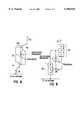
- FIG. 1is a perspective view of a SRAM cell array constructed in accordance with one embodiment of the present invention.
- FIG. 2is a circuit diagram illustrating one embodiment of a SRAM cell with latch-up and gated diode according to the present invention
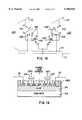
- FIG. 3is a cross-sectional view of the SRAM cell of FIG. 2 illustrating the regions and junctions of the semiconductor structure;
- FIG. 4is a schematic diagram illustrating the regions and features of the SRAM cell of FIG. 2;
- FIG. 5is a graph illustrating current-voltage characteristics and avalanche multiplication in the gated diode structure of the SRAM cell of FIG. 2;
- FIG. 6is a schematic diagram illustrating the regions involved in avalanche multiplication in the SRAM cell of FIG. 2;
- FIG. 7is a graph depicting the blocking, write and latch-up states of the SRAM cell of FIG. 2;
- FIG. 8is a circuit diagram for the SRAM cell of FIG. 2 having gated diode induced latch-up;
- FIG. 9is a schematic diagram for the SRAM cell of FIG. 2 having gated diode induced latch-up;
- FIG. 10is a circuit diagram illustrating a SRAM cell array with interconnect circuitry
- FIG. 11is a circuit diagram illustrating a SRAM cell array with interconnect and peripheral circuitry
- FIG. 12is a circuit diagram illustrating a second embodiment of a SRAM cell with latch-up and gated diode, and a shared n-p-n emitter and row address according to the present invention
- FIG. 13is a cross-sectional view of the SRAM cell of FIG. 12 illustrating the regions and junctions of the semiconductor structure
- FIG. 14is a schematic diagram illustrating the regions and features of the SRAM cell of FIG. 12;
- FIG. 15is a circuit diagram illustrating a third embodiment of a SRAM cell with latch-up and gated diode, and a shared p-n-p emitter and row address according to the present invention
- FIG. 16is a cross-sectional view of the SRAM cell of FIG. 15 illustrating the regions and junctions of the semiconductor structure.
- FIG. 17is a schematic diagram illustrating the regions and features of the SRAM cell of FIG. 15.
- wafer or substrate used in the following descriptioninclude any semiconductor-based structure having an exposed silicon surface in which to form the structure of this invention.
- Wafer and substrateare to be understood as including silicon-on-insulator, doped and undoped semiconductors, epitaxial layers of silicon supported by a base semiconductor foundation, and other semiconductor structures.
- previous process stepsmay have been utilized to form regions/junctions in the base-semiconductor structure or foundation. The following detailed description is, therefore, not to be taken in a limiting sense, and the scope of the present invention is defined by the appended claims.
- the array 10is comprised of a plurality of planar parasitic bipolar transistor pairs 12 on p-type silicon substrate 14. Planar transistor pairs or devices, noted generally 12, are separated from each other by isolation trenches 16, 18. Each parasitic bipolar transistor device 12 has dimensions of one F by four F, and each isolation trench 16, 18 is preferably one F wide. Thus, with the inclusion of transistor to transistor -isolation, the area per programmed device cell is 10F 2 (2F ⁇ 5F).
- a dual transistor memory cellcomprises two complementary bipolar transistors 22, 24 connected with a gate 28 to form a gated diode 26.
- Each memory cell 20is connected to other memory cells via three sets of interconnects.
- Column address line 30is connected to the emitter of transistor 22
- row address line 32is connected to the emitter of transistor 24, and write row address line 34 is connected to the gate 28 of gated diode 26.
- p+ region 40, n-region 42, and p-region 44comprise a lateral p-n-p bipolar transistor 22; and n+ region 46, p-region 44, and n-region 42 comprise a vertical n-p-n bipolar transistor 24.
- N-region 42underlies p-region 44, and is preferably formed as a retrograde n-well, meaning that the dopant is graded in the vertical direction with higher concentrations at the bottom of the well.
- the transistors 22, 24are connected so that the collector of transistor 22 is connected to the base of transistor 24, and vice-versa, as shown in FIGS. 1, 2 and 8.
- the interface between p+ region 40 and n-region 42comprises a first junction J1
- the interface between n-region 42 and p-region 44comprises a second junction J2
- the interface between p-region 44 and n+ region 46comprises a third junction J3.
- the second junction J2acts as a collector of holes from the first junction J1 and of electrons from the third junction J3.
- a gated diode 26is formed by gating the second junction J2 with a polysilicon gate 28. At equilibrium there is a depletion region at each junction, with a built-in potential determined by the impurity doping profile. When a positive voltage is applied to the anode 40, the second junction J2 will become reverse-biased, while the first and third junctions J1, J3 will be forward-biased.
- FIG. 4provides a schematic view of the dual transistor memory cell 20.
- the planar structure depictedhas an area of 10F 2 , a significant improvement over the prior art cells of 50 to 100 F 2 .
- the dual transistor memory cell 20operates as described hereinafter, and can best be understood by referencing FIGS. 5 through 11. Operation of the cell takes advantage of latch-up between the two complementary transistors to construct a compact SRAM cell.
- the cellwill block and not become latched-up until the power supply voltage, V DD , becomes very high.
- the cellcan be induced to latch-up at lower voltages by the application of a pulsed gate bias, thus inducing avalanche multiplication and breakdown in the gated diode structure 26.
- the breakdown voltage of an abrupt planar junction with a doping on the lightly doped side of the junction (n-type region 42 in FIG. 3) of ⁇ 1.5 ⁇ 10 17 cm -3is approximately 8 volts.
- band to band tunnelingoccurs and thus places a higher limit on the desired doping, as indicated by line 66.
- the doping of the heavily doped sideshould preferably have a concentration of 1 ⁇ 10 19 cm -3 in order to achieve an abrupt junction.
- Base currentcan be generated by introducing a pulsed gate bias and higher column voltage that initiates current multiplication in the gated diode.
- the pulse levelmust be calculated to yield sufficient current so that the sum of the common base current gains, ⁇ 1 and ⁇ 2 , of bipolar transistors 22, 24 exceeds one.
- the bias applied to induce latch-upis "pulsed" in the sense that it is only applied to initiate latch-up. As shown in FIG. 7, the cell is stable in the latched-up condition as a result of the pulse-initiated latch-up, which occurs during the "write” operation as discussed below.
- the collector and base currents (I C and I B , respectively) and the common base forward current transfer ratios or "current gain" ⁇ 1 and ⁇ 2are shown in FIG. 8. From FIG. 8, the collector current of the n-p-n transistor 24 provides the base drive for the p-n-p transistor 22. Also, the collector current of the p-n-p transistor 22 supplies the base drive for the n-p-n transistor 24.
- the base current of p-n-p transistor 22, IB 1is given by
- n-p-n transistor 24which is supplied by the collector of n-p-n transistor 24.
- the collector current of n-p-n transistor 24 with a common base current gain, ⁇ 2is given by
- the array structure of the CMOS SRAMincludes column decoder 68 and row decoder 70.
- the cellWhen the cell is not addressed, it is maintained in a low voltage state with V DD around 0.7 V to 0.8 V from the column address line 30 and the row address line 32 to reduce power consumption. Data is read by addressing a row and a column and increasing the power supply voltage across device 20 to 0.9 V or more at the coincidence of the column address line 30 and the row address line 32. If the cell is latched-up, a large current will be sensed between these row and column lines. If not latched-up, there will be little extra current.
- Writeis accomplished by raising the voltage across the cell at the coincidence of the write row address line 34 and column address line 30, to induce carrier multiplication in the gated diode 26.
- the high voltageinduces avalanche breakdown in the gated diode 26, and turns the transistors on strongly. The transistors then latch-up, so that the cell now will be read as storing a "one.”
- the voltage in the write row address line 34may be immediately lowered once the write operation is completed.
- transistor devices 20will provide about 100 ⁇ A of current. If this is read in 1.6 nanoseconds, then the total signal will be one million electrons, which is comparable to the read signal in DRAMs and easily sensed above any noise.
- a 4F 2 cellwill result in an area of less than 1 cm 2 for a 128 Mbit SRAM in 0.2 micron technology. If the standby current in each cell is 10 nanoamperes, then the standby current will be 1.28 A and the power dissipation about 1 Watt or 1 Watt/cm 2 , which is easily dissipated.
- a ratio of read current to standby current of 100 ⁇ A/0.01 ⁇ Acan be achieved since the read current is an exponential function of voltage, as shown in FIG. 7.
- a second embodiment of the present inventioninvolves the interconnection of two memory cells so that they share a common n-p-n emitter, as shown in FIGS. 12 and 13.
- Each parasitic bipolar transistor device 120, 120'comprises two complementary bipolar transistors 122, 124 connected with a gate 128 to form a gated diode 126.
- Each transistor device 120is connected to another transistor device 120' via a shared emitter region 146, as can best be seen by reference to FIGS. 12 and 13.
- Column address lines 30 and 30'are connected to the emitters of transistors 122 and 122', respectively, while row address line 32 is connected to the common emitter of transistors 124 and 124'.
- Write row address line 34is connected to the gates 128 and 128' of the gated diodes 126 and 126'.
- p+ region 140, n-region 142, and p-region 144comprise a p-n-p bipolar transistor 122; n+ region 146, p-region 144, and n-region 142 comprise an n-p-n bipolar transistor 124; n+ region 146, p-region 148, and n-region 150 comprise an n-p-n bipolar transistor 124'; and p-region 148, n-region 150, and p+ region 152 comprise a p-n-p bipolar transistor 122'.
- the transistors 122, 124are connected so that the collector of transistor 124 is connected to the base of transistor 122, and vice-versa.
- Transistors 122', 124'are interconnected in a similar fashion. In addition, transistors 124, 124' share the same emitter n+ region 146 that is connected to the row address line 32.
- the linked bipolar transistor devices 120, 120'function similarly to the single unlinked cell of the first embodiment. Because the write row address line 34 is still individually connected to each cell, and because each of the read and write operations operates at the coincidence of a column and a row, functioning of the devices 120 and 120' is not affected by their linkage.
- the shared emitter region 146 and shared row addressenable the cells to be manufactured in a denser array.
- the linked cellsmay be formed as a silicon-on-insulator (SOI) structure, with a layer of oxide 113 between the device and the underlying substrate 114 serving to isolate the device and permit denser packing of cells.
- SOIsilicon-on-insulator
- the two interlinked cells 120, 120'have a total area of 16F 2 , resulting in a per cell area of 8F 2 .
- a third embodiment of the present inventioninvolves the interconnection of two memory cells so that they share a common p-n-p emitter, as shown in FIGS. 15 and 16.
- Each parasitic bipolar transistor device 220, 220'comprises two complementary bipolar transistors 222, 224 connected with a gate 228 to form a gated diode 226.
- the transistor device 220is connected to another transistor device 220' via a shared emitter region 246, as can best be seen by reference to FIGS. 15 and 16.
- Column address lines 30 and 30'are connected to the emitters of transistors 222 and 222', respectively, while row address line 32 is connected to the common emitter of transistors 224 and 224'.
- Write row address line 34is connected to the gates 228 and 228' of the gated diodes 226 and 226'.
- n+ region 240, p-region 242, and n-region 244comprise an n-p-n bipolar transistor 222; p+ region 246, n-region 244, and p-region 242 comprise a p-n-p bipolar transistor 224; p+ region 246, n-region 248, and p-region 250 comprise a p-n-p bipolar transistor 224'; and n-region 248, p-region 250, and n+ region 252 comprise an n-p-n bipolar transistor 222'.
- the transistors 222, 224are connected so that the collector of transistor 224 is connected to the base of transistor 222, and vice-versa.
- Transistors 222', 224'are interconnected in a similar fashion. In addition, transistors 224, 224' share the same emitter p+ region 246 that is connected to the row address line 32.
- the linked bipolar transistor devices 220, 220'function similarly to the single, unlinked cell of the first embodiment. Because the write row address line 34 is still individually connected to each cell, and because each of the read and write operations operates at the coincidence of a column and a row, functioning of the devices 220, 220' is not affected by their linkage.
- the shared emitter region 246 and shared row addressenable the cells to be manufactured in a denser array.
- the linked cellsmay be formed as a silicon-on-insulator (SOI) structure, with a layer of oxide 213 between the device and the underlying substrate 214 serving to isolate the device and permit denser packing of cells.
- Two interlinked cells 220, 220'have a total area of 16F 2 , resulting in a per cell area of 8F 2 .
- the device array 10 of the first embodimentis manufactured through an exemplary process described as follows, resulting in the complete structure shown in FIG. 1. It is to be understood, however, that this process is only one example of many possible processes. For example, although the process as described begins with a p-type substrate, other processes may begin with a silicon-on-insulator (SOI) substrate. Another example is that a CMOS process involving standard twin-well process technology may be used instead of the disclosed process. Variants of the masking and etching processes are also contemplated, as is the use of conventional wells instead of implanted wells. The following description is, therefore, not to be taken in a limiting sense, and the scope of the present invention is defined by the appended claims.
- SOIsilicon-on-insulator
- a silicon substrate 14is selected as the base for the device array 10.
- the silicon substrate 14may be doped or undoped, but a doped p-type wafer is preferred.
- a thin oxide layeris grown on top of the silicon substrate by means of thermal oxidation, or other suitable means.
- a silicon nitride (Si 3 N 4 ) (“nitride”) layeris then formed, by chemical vapor deposition (CVD) or other deposition means, on top of the oxide layer.
- a photoresist and maskare applied, and photolithographic techniques are used to define areas to be etched-out. Etching is then carried out to etch through the nitride and oxide layers to expose trenches 16, 18 in which field oxide is to be formed.
- the photoresist and maskare then removed, and field oxide is then formed in the exposed trenches 16, 18, by a suitable process such as low-pressure CVD of silicon dioxide or thermal oxidation of the exposed substrate 14.
- a photoresist and maskare then applied to cover areas not to be doped in the following steps.
- N-wellsare then formed by high-energy ion implantation of arsenic, phosphorus or antimony into the exposed areas. Retrograde doping, where the concentration of n-dopant is highest at the bottom of the well, is achieved by extremely high-energy ion implantation at the MeV level.
- the photoresist and maskare then removed, and new photoresist and mask are applied to cover areas that are not to be counter-doped to form p-regions inside the n-wells, such as p-regions 40 and 44 shown in FIG. 1. Ion implantation of boron is then performed to counter-dope the exposed regions and form p-regions. The photoresist and mask are then removed, and new photoresist and mask are applied to cover areas that are not to be counter-doped to form n-regions inside some of the p-regions, such as the n+region 46 shown in FIG. 1.
- Ion implantation of arsenic, phosphorus or antimonyis then performed to counter-dope the exposed regions and form n-regions 46.
- the four regions of each device 20have now been formed, as the formation of the regions 40, 44, and 46 inside the n-well leaves the remaining area of the n-well as region 42 of the device 20.
- a gate 28is then formed over the central n-p junction J2 of each device 20.
- a thin gate oxide layeris formed on top of the junction by a suitable means, and then a polysilicon layer is deposited to serve as a gate layer.
- the device array 10then undergoes a finishing process. Selective etching with hot phosphoric acid or another suitable etchant is performed to remove any remaining masking layers or nitride layers from the top surface of the devices 20. If necessary, planarization by chemical-mechanical polishing or other suitable processes may be performed. Conventional processing methods may then be used to form contact holes and metal wiring to connect the devices.
- the final structure of the device array 10is as shown in FIG. 1.
Landscapes
- Semiconductor Memories (AREA)
Abstract
Description
I.sub.B1 =(1-α.sub.1)I.sub.A
I.sub.C2= α.sub.2 I.sub.K
I.sub.B1 -I.sub.AVALANCHE =I.sub.C2
Claims (47)
Priority Applications (2)
| Application Number | Priority Date | Filing Date | Title |
|---|---|---|---|
| US09/076,745US6104045A (en) | 1998-05-13 | 1998-05-13 | High density planar SRAM cell using bipolar latch-up and gated diode breakdown |
| US09/609,813US6773968B1 (en) | 1998-05-13 | 2000-07-03 | High density planar SRAM cell using bipolar latch-up and gated diode breakdown |
Applications Claiming Priority (1)
| Application Number | Priority Date | Filing Date | Title |
|---|---|---|---|
| US09/076,745US6104045A (en) | 1998-05-13 | 1998-05-13 | High density planar SRAM cell using bipolar latch-up and gated diode breakdown |
Related Child Applications (1)
| Application Number | Title | Priority Date | Filing Date |
|---|---|---|---|
| US09/609,813DivisionUS6773968B1 (en) | 1998-05-13 | 2000-07-03 | High density planar SRAM cell using bipolar latch-up and gated diode breakdown |
Publications (1)
| Publication Number | Publication Date |
|---|---|
| US6104045Atrue US6104045A (en) | 2000-08-15 |
Family
ID=22133920
Family Applications (2)
| Application Number | Title | Priority Date | Filing Date |
|---|---|---|---|
| US09/076,745Expired - LifetimeUS6104045A (en) | 1998-05-13 | 1998-05-13 | High density planar SRAM cell using bipolar latch-up and gated diode breakdown |
| US09/609,813Expired - Fee RelatedUS6773968B1 (en) | 1998-05-13 | 2000-07-03 | High density planar SRAM cell using bipolar latch-up and gated diode breakdown |
Family Applications After (1)
| Application Number | Title | Priority Date | Filing Date |
|---|---|---|---|
| US09/609,813Expired - Fee RelatedUS6773968B1 (en) | 1998-05-13 | 2000-07-03 | High density planar SRAM cell using bipolar latch-up and gated diode breakdown |
Country Status (1)
| Country | Link |
|---|---|
| US (2) | US6104045A (en) |
Cited By (61)
| Publication number | Priority date | Publication date | Assignee | Title |
|---|---|---|---|---|
| US6465864B2 (en)* | 2001-02-13 | 2002-10-15 | Faraday Technology Corp. | Diode structure on MOS wafer |
| US20030048657A1 (en)* | 2001-08-28 | 2003-03-13 | Leonard Forbes | Four terminal memory cell, a two-transistor SRAM cell, a SRAM array, a computer system, a process for forming a SRAM cell, a process for turning a SRAM cell off, a process for writing a SRAM cell and a process for reading data from a SRAM cell |
| US6552398B2 (en)* | 2001-01-16 | 2003-04-22 | Ibm Corporation | T-Ram array having a planar cell structure and method for fabricating the same |
| US20030094655A1 (en)* | 2000-04-27 | 2003-05-22 | Jukka Pekola | Method for measuring temperature in a wide range using a tunnel junction |
| US20030129215A1 (en)* | 1998-09-24 | 2003-07-10 | T-Ram, Inc. | Medical devices containing rapamycin analogs |
| US20030141545A1 (en)* | 2002-01-11 | 2003-07-31 | Seiko Epson Corporation | Semiconductor device |
| US6654275B2 (en) | 2001-03-15 | 2003-11-25 | Micron Technology, Inc. | SRAM cell with horizontal merged devices |
| US6653665B2 (en) | 2001-02-13 | 2003-11-25 | Kabushiki Kaisha Toshiba | Memory device |
| US6666481B1 (en) | 2002-10-01 | 2003-12-23 | T-Ram, Inc. | Shunt connection to emitter |
| US20040010186A1 (en)* | 2002-07-11 | 2004-01-15 | Optical Sensors, Inc. | Calibration technique for non-invasive medical devices |
| US6683330B1 (en) | 2002-10-01 | 2004-01-27 | T-Ram, Inc. | Recessed thyristor control port |
| US6686612B1 (en) | 2002-10-01 | 2004-02-03 | T-Ram, Inc. | Thyristor-based device adapted to inhibit parasitic current |
| US6690039B1 (en) | 2002-10-01 | 2004-02-10 | T-Ram, Inc. | Thyristor-based device that inhibits undesirable conductive channel formation |
| US20040041206A1 (en)* | 2002-08-30 | 2004-03-04 | Micron Technology, Inc. | One transistor SOI non-volatile random access memory cell |
| US20040041212A1 (en)* | 2002-08-30 | 2004-03-04 | Arup Bhattacharyya | Gated lateral thyristor-based random access memory cell (GLTRAM) |
| US20040041208A1 (en)* | 2002-08-30 | 2004-03-04 | Arup Bhattacharyya | One transistor SOI non-volatile random access memory cell |
| US20040042268A1 (en)* | 2002-08-30 | 2004-03-04 | Arup Bhattacharyya | One-device non-volatile random access memory cell |
| US6703646B1 (en) | 2002-09-24 | 2004-03-09 | T-Ram, Inc. | Thyristor with lightly-doped emitter |
| US6756612B1 (en) | 2002-10-28 | 2004-06-29 | T-Ram, Inc. | Carrier coupler for thyristor-based semiconductor device |
| US20040171219A1 (en)* | 1998-05-13 | 2004-09-02 | Noble Wendell P. | High density SRAM cell with latched vertical transistors |
| US6790713B1 (en) | 2002-09-09 | 2004-09-14 | T-Ram, Inc. | Method for making an inlayed thyristor-based device |
| US6815734B1 (en) | 2002-10-01 | 2004-11-09 | T-Ram, Inc. | Varied trench depth for thyristor isolation |
| US6818482B1 (en) | 2002-10-01 | 2004-11-16 | T-Ram, Inc. | Method for trench isolation for thyristor-based device |
| US6828202B1 (en) | 2002-10-01 | 2004-12-07 | T-Ram, Inc. | Semiconductor region self-aligned with ion implant shadowing |
| US6835997B1 (en) | 2001-03-22 | 2004-12-28 | T-Ram, Inc. | Thyristor-based device with trench dielectric material |
| US20050001232A1 (en)* | 2003-07-02 | 2005-01-06 | Micron Technology, Inc. | High-performance one-transistor memory cell |
| US6845026B1 (en) | 2003-05-30 | 2005-01-18 | Netlogic Microsystems, Inc. | Thyristor-based content addressable memory (CAM) cells |
| US6888177B1 (en) | 2002-09-24 | 2005-05-03 | T-Ram, Inc. | Increased base-emitter capacitance |
| US6891205B1 (en) | 2001-03-22 | 2005-05-10 | T-Ram, Inc. | Stability in thyristor-based memory device |
| US20050111863A1 (en)* | 2003-11-21 | 2005-05-26 | Sakae Ogashima | Fixing unit and image forming apparatus |
| US6913955B1 (en) | 2002-10-01 | 2005-07-05 | T-Ram, Inc. | Method of manufacturing a thyristor device with a control port in a trench |
| US6953953B1 (en) | 2002-10-01 | 2005-10-11 | T-Ram, Inc. | Deep trench isolation for thyristor-based semiconductor device |
| US6980457B1 (en) | 2002-11-06 | 2005-12-27 | T-Ram, Inc. | Thyristor-based device having a reduced-resistance contact to a buried emitter region |
| US6998652B1 (en) | 2002-10-01 | 2006-02-14 | T-Ram, Inc. | Trench isolation for thyristor-based device |
| US7030425B1 (en) | 2002-10-01 | 2006-04-18 | Tram, Inc. | Buried emitter contact for thyristor-based semiconductor device |
| US7053423B1 (en) | 2002-09-24 | 2006-05-30 | T-Ram, Inc. | Thyristor having a first emitter with relatively lightly doped portion to the base |
| US20060192591A1 (en)* | 2005-02-28 | 2006-08-31 | International Business Machines Corporation | Logic circuits utilizing gated diode sensing |
| US20060227601A1 (en)* | 2004-08-24 | 2006-10-12 | Micron Technology, Inc. | Memory cell with trenched gated thyristor |
| US20060239068A1 (en)* | 2005-04-21 | 2006-10-26 | Micron Technology, Inc. | Static random access memory cell |
| US7135745B1 (en)* | 2002-09-09 | 2006-11-14 | T-Ram, Inc. | Fin thyristor-based semiconductor device |
| US7193922B2 (en)* | 2002-06-03 | 2007-03-20 | Fujitsu Limited | Semiconductor integrated circuit |
| US7209384B1 (en) | 2005-12-08 | 2007-04-24 | Juhan Kim | Planar capacitor memory cell and its applications |
| US20070120173A1 (en)* | 2005-11-28 | 2007-05-31 | Bohumil Lojek | Non-volatile memory cell with high current output line |
| US7268373B1 (en)* | 2003-11-12 | 2007-09-11 | T-Ram Semiconductor, Inc. | Thyristor-based memory and its method of operation |
| US20070249115A1 (en)* | 2006-04-21 | 2007-10-25 | International Business Machines Corporation | Dynamic memory cell structures |
| US7374974B1 (en) | 2001-03-22 | 2008-05-20 | T-Ram Semiconductor, Inc. | Thyristor-based device with trench dielectric material |
| US20080251830A1 (en)* | 2007-04-13 | 2008-10-16 | Kabushiki Kaisha Toshiba | Semiconductor storage device and driving method thereof |
| US20080291751A1 (en)* | 2003-08-07 | 2008-11-27 | Daniel Robert Shepard | Scr matrix storage device |
| US7460395B1 (en) | 2005-06-22 | 2008-12-02 | T-Ram Semiconductor, Inc. | Thyristor-based semiconductor memory and memory array with data refresh |
| US7728626B2 (en) | 2002-07-08 | 2010-06-01 | Micron Technology, Inc. | Memory utilizing oxide nanolaminates |
| US7894255B1 (en) | 2005-06-22 | 2011-02-22 | T-Ram Semiconductor, Inc. | Thyristor based memory cell |
| US7894256B1 (en) | 2005-06-22 | 2011-02-22 | T-Ram Semiconductor, Inc. | Thyristor based memory cell |
| US20110051540A1 (en)* | 2009-09-01 | 2011-03-03 | Xiaowei Deng | Method and structure for SRAM cell trip voltage measurement |
| US8093107B1 (en) | 2005-06-22 | 2012-01-10 | T-Ram Semiconductor, Inc. | Thyristor semiconductor memory and method of manufacture |
| US20120061639A1 (en)* | 2010-09-14 | 2012-03-15 | Naoki Yasuda | Resistance change memory |
| US8767458B2 (en)* | 2010-11-16 | 2014-07-01 | Zeno Semiconductor, Inc. | Dual-port semiconductor memory and first in first out (FIFO) memory having electrically floating body transistor |
| US20140217502A1 (en)* | 2013-02-07 | 2014-08-07 | International Business Machines Corporation | Diode Structure and Method for Wire-Last Nanomesh Technologies |
| US9153333B2 (en) | 2007-10-24 | 2015-10-06 | Zeno Semiconductor, Inc. | Semiconductor memory having both volatile and non-volatile functionality and method of operating |
| US20160049403A1 (en)* | 2014-08-14 | 2016-02-18 | Gil Asa | Cmos compatible memory cells |
| US20170005187A1 (en)* | 2014-01-24 | 2017-01-05 | Walid M. Hafez | Fin-based semiconductor devices and methods |
| US10058641B2 (en) | 2001-09-10 | 2018-08-28 | Abbott Laboratories | Medical devices containing rapamycin analogs |
Families Citing this family (3)
| Publication number | Priority date | Publication date | Assignee | Title |
|---|---|---|---|---|
| US7732877B2 (en)* | 2007-04-02 | 2010-06-08 | Taiwan Semiconductor Manufacturing Company, Ltd. | Gated diode with non-planar source region |
| US8394683B2 (en) | 2008-01-15 | 2013-03-12 | Micron Technology, Inc. | Methods of forming semiconductor constructions, and methods of forming NAND unit cells |
| TWI668803B (en)* | 2016-12-13 | 2019-08-11 | 鈺創科技股份有限公司 | Memory circuit with thyristor |
Citations (15)
| Publication number | Priority date | Publication date | Assignee | Title |
|---|---|---|---|---|
| US4543595A (en)* | 1982-05-20 | 1985-09-24 | Fairchild Camera And Instrument Corporation | Bipolar memory cell |
| US4720845A (en)* | 1986-04-23 | 1988-01-19 | Siemens Aktiengesellschaft | Protective circuit for the overvoltage protection of a subscriber line interconnect circuit |
| US5173754A (en)* | 1992-02-03 | 1992-12-22 | Micron Technology, Inc. | Integrated circuit device with gate in sidewall |
| US5214295A (en)* | 1992-01-28 | 1993-05-25 | Micron Technology, Inc. | Thin film field effect transistor, CMOS inverter, and methods of forming thin film field effect transistors and CMOS inverters |
| US5286663A (en)* | 1992-01-29 | 1994-02-15 | Micron Technology, Inc. | Methods for producing thin film transistor having a diode shunt |
| US5486717A (en)* | 1993-10-29 | 1996-01-23 | Mitsubishi Denki Kabushiki Kaisha | SRAM with small planar layout |
| US5497011A (en)* | 1994-09-19 | 1996-03-05 | Mitsubishi Denki Kabushiki Kaisha | Semiconductor memory device and a method of using the same |
| US5535156A (en)* | 1994-05-05 | 1996-07-09 | California Institute Of Technology | Transistorless, multistable current-mode memory cells and memory arrays and methods of reading and writing to the same |
| US5581104A (en)* | 1991-01-16 | 1996-12-03 | Micron Technology, Inc. | Static discharge circuit having low breakdown voltage bipolar clamp |
| US5594683A (en)* | 1995-04-07 | 1997-01-14 | Chen; Ming-Jer | SRAM cell using a CMOS compatible high gain gated lateral BJT |
| US5624863A (en)* | 1995-07-17 | 1997-04-29 | Micron Technology, Inc. | Semiconductor processing method of forming complementary N-type doped and P-type doped active regions within a semiconductor substrate |
| US5650350A (en)* | 1995-08-11 | 1997-07-22 | Micron Technology, Inc. | Semiconductor processing method of forming a static random access memory cell and static random access memory cell |
| US5684737A (en)* | 1995-12-08 | 1997-11-04 | The Regents Of The University Of California | SRAM cell utilizing bistable diode having GeSi structure therein |
| US5705843A (en)* | 1995-03-23 | 1998-01-06 | Micron Technology, Inc. | Integrated circuits and SRAM memory cells |
| US5710741A (en)* | 1994-03-11 | 1998-01-20 | Micron Technology, Inc. | Power up intialization circuit responding to an input signal |
Family Cites Families (10)
| Publication number | Priority date | Publication date | Assignee | Title |
|---|---|---|---|---|
| JPS5233466A (en)* | 1975-09-10 | 1977-03-14 | Hitachi Ltd | Semiconductor switch |
| JPS5511331A (en)* | 1978-07-11 | 1980-01-26 | Hitachi Ltd | Method of manufacturing semiconductor integrated circuit |
| JPS55166957A (en)* | 1979-06-13 | 1980-12-26 | Nec Corp | Planar type thyristor |
| JPS63292675A (en)* | 1987-05-25 | 1988-11-29 | Nec Corp | Planar thyristor |
| US4861731A (en)* | 1988-02-02 | 1989-08-29 | General Motors Corporation | Method of fabricating a lateral dual gate thyristor |
| US5278076A (en)* | 1990-02-28 | 1994-01-11 | At&T Bell Laboratories | Method of marking a lateral mos controlled thyristor |
| JPH04284669A (en)* | 1991-03-14 | 1992-10-09 | Fuji Electric Co Ltd | Insulated-gate control thyristor |
| FR2729008B1 (en)* | 1994-12-30 | 1997-03-21 | Sgs Thomson Microelectronics | INTEGRATED POWER CIRCUIT |
| US5777346A (en)* | 1996-01-16 | 1998-07-07 | Harris Corporation | Metal oxide semiconductor controlled thyristor with an on-field effect transistor in a trench |
| FR2744287B1 (en)* | 1996-01-26 | 1998-04-30 | Sgs Thomson Microelectronics | SIDE COMPONENTS IN A SEMICONDUCTOR POWER DEVICE |
- 1998
- 1998-05-13USUS09/076,745patent/US6104045A/ennot_activeExpired - Lifetime
- 2000
- 2000-07-03USUS09/609,813patent/US6773968B1/ennot_activeExpired - Fee Related
Patent Citations (15)
| Publication number | Priority date | Publication date | Assignee | Title |
|---|---|---|---|---|
| US4543595A (en)* | 1982-05-20 | 1985-09-24 | Fairchild Camera And Instrument Corporation | Bipolar memory cell |
| US4720845A (en)* | 1986-04-23 | 1988-01-19 | Siemens Aktiengesellschaft | Protective circuit for the overvoltage protection of a subscriber line interconnect circuit |
| US5581104A (en)* | 1991-01-16 | 1996-12-03 | Micron Technology, Inc. | Static discharge circuit having low breakdown voltage bipolar clamp |
| US5214295A (en)* | 1992-01-28 | 1993-05-25 | Micron Technology, Inc. | Thin film field effect transistor, CMOS inverter, and methods of forming thin film field effect transistors and CMOS inverters |
| US5286663A (en)* | 1992-01-29 | 1994-02-15 | Micron Technology, Inc. | Methods for producing thin film transistor having a diode shunt |
| US5173754A (en)* | 1992-02-03 | 1992-12-22 | Micron Technology, Inc. | Integrated circuit device with gate in sidewall |
| US5486717A (en)* | 1993-10-29 | 1996-01-23 | Mitsubishi Denki Kabushiki Kaisha | SRAM with small planar layout |
| US5710741A (en)* | 1994-03-11 | 1998-01-20 | Micron Technology, Inc. | Power up intialization circuit responding to an input signal |
| US5535156A (en)* | 1994-05-05 | 1996-07-09 | California Institute Of Technology | Transistorless, multistable current-mode memory cells and memory arrays and methods of reading and writing to the same |
| US5497011A (en)* | 1994-09-19 | 1996-03-05 | Mitsubishi Denki Kabushiki Kaisha | Semiconductor memory device and a method of using the same |
| US5705843A (en)* | 1995-03-23 | 1998-01-06 | Micron Technology, Inc. | Integrated circuits and SRAM memory cells |
| US5594683A (en)* | 1995-04-07 | 1997-01-14 | Chen; Ming-Jer | SRAM cell using a CMOS compatible high gain gated lateral BJT |
| US5624863A (en)* | 1995-07-17 | 1997-04-29 | Micron Technology, Inc. | Semiconductor processing method of forming complementary N-type doped and P-type doped active regions within a semiconductor substrate |
| US5650350A (en)* | 1995-08-11 | 1997-07-22 | Micron Technology, Inc. | Semiconductor processing method of forming a static random access memory cell and static random access memory cell |
| US5684737A (en)* | 1995-12-08 | 1997-11-04 | The Regents Of The University Of California | SRAM cell utilizing bistable diode having GeSi structure therein |
Non-Patent Citations (19)
| Title |
|---|
| (For both A and B citations above published in IEEE 1998, Symposium on VLSI Technology, Honolulu, Hawaii, Jun. 9th and 11th, 1998).* |
| (For both A and B citations above--published in IEEE 1998, Symposium on VLSI Technology, Honolulu, Hawaii, Jun. 9th and 11th, 1998). |
| D. L. Hetherington et al, An Integrated GaAs N P N P Thyristor/JFET Memory Cell Exhibiting Nondestructive Read, IEEE Electron Device Letters, vol. 13, No. 9, Sep. 1992.* |
| D. L. Hetherington et al, An Integrated GaAs N-P-N-P Thyristor/JFET Memory Cell Exhibiting Nondestructive Read, IEEE Electron Device Letters, vol. 13, No. 9, Sep. 1992. |
| Farid Nemati et al, "A Novel High Density, Low Voltage SRAM Cell With a Vertical NDR Device", Center for Integrated Systems, Stanford University, CA, (2 pages). |
| Farid Nemati et al, A Novel High Density, Low Voltage SRAM Cell With a Vertical NDR Device , Center for Integrated Systems, Stanford University, CA, (2 pages).* |
| Hyun Jin Cho et al, A Novel Pillar DRAM Cell for 4GBIT and Beyond , Center for Integrated Systems, Stanford University, CA, (2 pages).* |
| Hyun-Jin Cho et al, "A Novel Pillar DRAM Cell for 4GBIT and Beyond", Center for Integrated Systems, Stanford University, CA, (2 pages). |
| I.T. Ho et al, Single Thyuristor Static Memory and its Fabrication, vol. 23, No.3, 1980.* |
| J.J. Ebers, Four Terminal P N P N Transistors, Proceedings of IRE, Nov. 1952, pp. 1361 1364.* |
| J.J. Ebers, Four-Terminal P-N-P-N Transistors, Proceedings of IRE, Nov. 1952, pp. 1361-1364. |
| R. C. Fang, Latchup Model for the Parasitic P N P N Path in Bulk CMOS, IEEE Transactions on Electron Devices, vol. Ed. 31, No. Jan. 1984.* |
| R. C. Fang, Latchup Model for the Parasitic P-N-P-N Path in Bulk CMOS, IEEE Transactions on Electron Devices, vol. Ed. 31, No. Jan. 1984. |
| R. R. Troutman et al. Transient Analysis of Latchup in Bulk CMOS, IEEE Transactions on Electron Devices, vol. Ed. 30, No. 2, Feb. 1993.* |
| S. M. Sze, Physics of Semiconductor Devices, Second Edition, A Wiley Interscience Pub. 1981.* |
| S. V. Vandebroek et al, High Gain Lateral Bipolar Action in a MOSFET Structure, IEEE Transactions on Electron Devices, vol. 38, No. 11, Nov. 1991.* |
| S. V. Vandebroek et al, High-Gain Lateral Bipolar Action in a MOSFET Structure, IEEE Transactions on Electron Devices, vol. 38, No. 11, Nov. 1991. |
| S.D. Malaviya, Single Device DC Stable Memory Cell, IBM Technical Disclosure Bulletin, vol. 20, No. 9, pp. 3492 3494, Nov. 1978.* |
| S.D. Malaviya, Single-Device DC Stable Memory Cell, IBM Technical Disclosure Bulletin, vol. 20, No. 9, pp. 3492-3494, Nov. 1978. |
Cited By (145)
| Publication number | Priority date | Publication date | Assignee | Title |
|---|---|---|---|---|
| US7105386B2 (en)* | 1998-05-13 | 2006-09-12 | Micron Technology, Inc. | High density SRAM cell with latched vertical transistors |
| US20040171219A1 (en)* | 1998-05-13 | 2004-09-02 | Noble Wendell P. | High density SRAM cell with latched vertical transistors |
| US20060216870A1 (en)* | 1998-05-13 | 2006-09-28 | Noble Wendell P Jr | High density SRAM cell with latched vertical transistors |
| US20030129215A1 (en)* | 1998-09-24 | 2003-07-10 | T-Ram, Inc. | Medical devices containing rapamycin analogs |
| US20030094655A1 (en)* | 2000-04-27 | 2003-05-22 | Jukka Pekola | Method for measuring temperature in a wide range using a tunnel junction |
| US6784012B2 (en) | 2000-04-27 | 2004-08-31 | Nanoway Oy | Method for measuring temperature in a wide range using a tunnel junction |
| US6552398B2 (en)* | 2001-01-16 | 2003-04-22 | Ibm Corporation | T-Ram array having a planar cell structure and method for fabricating the same |
| US6653665B2 (en) | 2001-02-13 | 2003-11-25 | Kabushiki Kaisha Toshiba | Memory device |
| US6465864B2 (en)* | 2001-02-13 | 2002-10-15 | Faraday Technology Corp. | Diode structure on MOS wafer |
| US20060067110A1 (en)* | 2001-03-15 | 2006-03-30 | Micron Technology, Inc. | SRAM cell with horizontal merged devices |
| US7020030B2 (en) | 2001-03-15 | 2006-03-28 | Micron Technology, Inc. | SRAM cell with horizontal merged devices |
| US6654275B2 (en) | 2001-03-15 | 2003-11-25 | Micron Technology, Inc. | SRAM cell with horizontal merged devices |
| US20040100816A1 (en)* | 2001-03-15 | 2004-05-27 | Micron Technology, Inc. | SRAM cell with horizontal merged devices |
| US7233531B2 (en) | 2001-03-15 | 2007-06-19 | Micro Technology, Inc. | SRAM cell with horizontal merged devices |
| US6891205B1 (en) | 2001-03-22 | 2005-05-10 | T-Ram, Inc. | Stability in thyristor-based memory device |
| US7374974B1 (en) | 2001-03-22 | 2008-05-20 | T-Ram Semiconductor, Inc. | Thyristor-based device with trench dielectric material |
| US6835997B1 (en) | 2001-03-22 | 2004-12-28 | T-Ram, Inc. | Thyristor-based device with trench dielectric material |
| US20040026697A1 (en)* | 2001-08-28 | 2004-02-12 | Leonard Forbes | Four terminal memory cell, a two-transistor SRAM cell, a SRAM array, a computer system, a process for forming a SRAM cell, a process for turning a SRAM cell off, a process for writing a SRAM cell and a process for reading data from a SRAM cell |
| US6919254B2 (en) | 2001-08-28 | 2005-07-19 | Micron Technology, Inc. | Computer systems, processes for forming a SRAM cell, processes for turning a SRAM cell off, processes for writing a SRAM cell and processes for reading data from a SRAM cell |
| US20050281069A1 (en)* | 2001-08-28 | 2005-12-22 | Leonard Forbes | Computer systems, processes for turning a SRAM cell off, and processes for writing a SRAM cell |
| US6999351B2 (en) | 2001-08-28 | 2006-02-14 | Micron Technology, Inc. | Computer systems, processes for turning a SRAM cell off, and processes for writing a SRAM cell and processes for reading data from a SRAM cell |
| US6888740B2 (en) | 2001-08-28 | 2005-05-03 | Micron Technology, Inc. | Two-transistor SRAM cells |
| US20030214840A1 (en)* | 2001-08-28 | 2003-11-20 | Leonard Forbes | Computer systems, processes for forming a SRAM cell, processes for turning a SRAM cell off, processes for writing a SRAM cell and processes for reading data from a SRAM cell |
| US20060193161A1 (en)* | 2001-08-28 | 2006-08-31 | Leonard Forbes | Processes for turning a SRAM cell off and processess for writing a SRAM cell |
| US20030048657A1 (en)* | 2001-08-28 | 2003-03-13 | Leonard Forbes | Four terminal memory cell, a two-transistor SRAM cell, a SRAM array, a computer system, a process for forming a SRAM cell, a process for turning a SRAM cell off, a process for writing a SRAM cell and a process for reading data from a SRAM cell |
| US20040196683A1 (en)* | 2001-08-28 | 2004-10-07 | Micron Technology, Inc. | Computer systems, processes for turning a SRAM cell off, and processes for writing a SRAM cell and processes for reading data from a SRAM cell |
| US6813180B2 (en)* | 2001-08-28 | 2004-11-02 | Micron Technology, Inc. | Four terminal memory cell, a two-transistor sram cell, a sram array, a computer system, a process for forming a sram cell, a process for turning a sram cell off, a process for writing a sram cell and a process for reading data from a sram cell |
| US7164597B2 (en) | 2001-08-28 | 2007-01-16 | Micron Technology, Inc. | Computer systems |
| US10058641B2 (en) | 2001-09-10 | 2018-08-28 | Abbott Laboratories | Medical devices containing rapamycin analogs |
| US6894351B2 (en)* | 2002-01-11 | 2005-05-17 | Seiko Epson Corporation | Semiconductor device for electrostatic protection |
| US20030141545A1 (en)* | 2002-01-11 | 2003-07-31 | Seiko Epson Corporation | Semiconductor device |
| US7193922B2 (en)* | 2002-06-03 | 2007-03-20 | Fujitsu Limited | Semiconductor integrated circuit |
| US8228725B2 (en) | 2002-07-08 | 2012-07-24 | Micron Technology, Inc. | Memory utilizing oxide nanolaminates |
| US7728626B2 (en) | 2002-07-08 | 2010-06-01 | Micron Technology, Inc. | Memory utilizing oxide nanolaminates |
| US20040010186A1 (en)* | 2002-07-11 | 2004-01-15 | Optical Sensors, Inc. | Calibration technique for non-invasive medical devices |
| US7485513B2 (en) | 2002-08-30 | 2009-02-03 | Micron Technology, Inc. | One-device non-volatile random access memory cell |
| US20040041208A1 (en)* | 2002-08-30 | 2004-03-04 | Arup Bhattacharyya | One transistor SOI non-volatile random access memory cell |
| US7456054B2 (en) | 2002-08-30 | 2008-11-25 | Micron Technology, Inc. | Gated lateral thyristor-based random access memory cell (GLTRAM) |
| US7184312B2 (en) | 2002-08-30 | 2007-02-27 | Micron Technology, Inc. | One transistor SOI non-volatile random access memory cell |
| US7130216B2 (en) | 2002-08-30 | 2006-10-31 | Micron Technology, Inc. | One-device non-volatile random access memory cell |
| US6888200B2 (en) | 2002-08-30 | 2005-05-03 | Micron Technology Inc. | One transistor SOI non-volatile random access memory cell |
| US20040042268A1 (en)* | 2002-08-30 | 2004-03-04 | Arup Bhattacharyya | One-device non-volatile random access memory cell |
| US7042027B2 (en) | 2002-08-30 | 2006-05-09 | Micron Technology, Inc. | Gated lateral thyristor-based random access memory cell (GLTRAM) |
| US20050026354A1 (en)* | 2002-08-30 | 2005-02-03 | Micron Technoloy Inc. | One transistor SOI non-volatile random access memory cell |
| US7566601B2 (en) | 2002-08-30 | 2009-07-28 | Micron Technology, Inc. | Method of making a one transistor SOI non-volatile random access memory cell |
| US6917078B2 (en) | 2002-08-30 | 2005-07-12 | Micron Technology Inc. | One transistor SOI non-volatile random access memory cell |
| US20050026353A1 (en)* | 2002-08-30 | 2005-02-03 | Micron Technology, Inc. | One transistor SOI non-volatile random access memory cell |
| US20060240653A1 (en)* | 2002-08-30 | 2006-10-26 | Micron Technology, Inc. | One-device non-volatile random access memory cell |
| US20050250261A1 (en)* | 2002-08-30 | 2005-11-10 | Micron Technology, Inc. | One transistor SOI non-volatile random access memory cell |
| US20050280023A1 (en)* | 2002-08-30 | 2005-12-22 | Micron Technology, Inc. | Gated lateral thyristor-based random access memory cell (GLTRAM) |
| US20040041212A1 (en)* | 2002-08-30 | 2004-03-04 | Arup Bhattacharyya | Gated lateral thyristor-based random access memory cell (GLTRAM) |
| US20040160825A1 (en)* | 2002-08-30 | 2004-08-19 | Micron Technology, Inc. | One-device non-volatile random access memory cell |
| US20040041206A1 (en)* | 2002-08-30 | 2004-03-04 | Micron Technology, Inc. | One transistor SOI non-volatile random access memory cell |
| US20070138555A1 (en)* | 2002-08-30 | 2007-06-21 | Micron Technology, Inc. | One transistor SOI non-volatile random access memory cell |
| US7339830B2 (en) | 2002-08-30 | 2008-03-04 | Micron Technology, Inc. | One transistor SOI non-volatile random access memory cell |
| US7440317B2 (en) | 2002-08-30 | 2008-10-21 | Micron Technology, Inc. | One transistor SOI non-volatile random access memory cell |
| US7968381B1 (en) | 2002-09-09 | 2011-06-28 | T-Ram Semiconductor, Inc. | Fin thyristor-based semiconductor device |
| US6790713B1 (en) | 2002-09-09 | 2004-09-14 | T-Ram, Inc. | Method for making an inlayed thyristor-based device |
| US7135745B1 (en)* | 2002-09-09 | 2006-11-14 | T-Ram, Inc. | Fin thyristor-based semiconductor device |
| US6703646B1 (en) | 2002-09-24 | 2004-03-09 | T-Ram, Inc. | Thyristor with lightly-doped emitter |
| US6888177B1 (en) | 2002-09-24 | 2005-05-03 | T-Ram, Inc. | Increased base-emitter capacitance |
| US7053423B1 (en) | 2002-09-24 | 2006-05-30 | T-Ram, Inc. | Thyristor having a first emitter with relatively lightly doped portion to the base |
| US6828176B1 (en) | 2002-09-24 | 2004-12-07 | T-Ram, Inc. | Thyristor having a first emitter with relatively lightly doped portion to the base |
| US6998652B1 (en) | 2002-10-01 | 2006-02-14 | T-Ram, Inc. | Trench isolation for thyristor-based device |
| US7049182B1 (en) | 2002-10-01 | 2006-05-23 | T-Ram, Inc. | Shunt connection to the emitter of a thyristor |
| US6666481B1 (en) | 2002-10-01 | 2003-12-23 | T-Ram, Inc. | Shunt connection to emitter |
| US6979602B1 (en) | 2002-10-01 | 2005-12-27 | T-Ram, Inc. | Method for making a recessed thyristor control port |
| US6953953B1 (en) | 2002-10-01 | 2005-10-11 | T-Ram, Inc. | Deep trench isolation for thyristor-based semiconductor device |
| US6913955B1 (en) | 2002-10-01 | 2005-07-05 | T-Ram, Inc. | Method of manufacturing a thyristor device with a control port in a trench |
| US7015077B1 (en) | 2002-10-01 | 2006-03-21 | T-Ram, Inc. | Varied trench depth for thyristor isolation |
| US6686612B1 (en) | 2002-10-01 | 2004-02-03 | T-Ram, Inc. | Thyristor-based device adapted to inhibit parasitic current |
| US6683330B1 (en) | 2002-10-01 | 2004-01-27 | T-Ram, Inc. | Recessed thyristor control port |
| US7030425B1 (en) | 2002-10-01 | 2006-04-18 | Tram, Inc. | Buried emitter contact for thyristor-based semiconductor device |
| US6828202B1 (en) | 2002-10-01 | 2004-12-07 | T-Ram, Inc. | Semiconductor region self-aligned with ion implant shadowing |
| US6818482B1 (en) | 2002-10-01 | 2004-11-16 | T-Ram, Inc. | Method for trench isolation for thyristor-based device |
| US6815734B1 (en) | 2002-10-01 | 2004-11-09 | T-Ram, Inc. | Varied trench depth for thyristor isolation |
| US7183591B1 (en) | 2002-10-01 | 2007-02-27 | T-Ram Semiconductor, Inc. | Trench isolation for thyristor-based device |
| US7351614B1 (en) | 2002-10-01 | 2008-04-01 | T-Ram Semiconductor, Inc. | Deep trench isolation for thyristor-based semiconductor device |
| US6690039B1 (en) | 2002-10-01 | 2004-02-10 | T-Ram, Inc. | Thyristor-based device that inhibits undesirable conductive channel formation |
| US6872602B1 (en) | 2002-10-28 | 2005-03-29 | T-Ram, Inc. | Carrier coupler for thyristor-based semiconductor device |
| US6756612B1 (en) | 2002-10-28 | 2004-06-29 | T-Ram, Inc. | Carrier coupler for thyristor-based semiconductor device |
| US6980457B1 (en) | 2002-11-06 | 2005-12-27 | T-Ram, Inc. | Thyristor-based device having a reduced-resistance contact to a buried emitter region |
| US6845026B1 (en) | 2003-05-30 | 2005-01-18 | Netlogic Microsystems, Inc. | Thyristor-based content addressable memory (CAM) cells |
| US20060244007A1 (en)* | 2003-07-02 | 2006-11-02 | Micron Technology, Inc. | High-performance one-transistor memory cell |
| US20060246653A1 (en)* | 2003-07-02 | 2006-11-02 | Micron Technology, Inc. | High-performance one-transistor memory cell |
| US7660144B2 (en) | 2003-07-02 | 2010-02-09 | Micron Technology, Inc. | High-performance one-transistor memory cell |
| US7728350B2 (en) | 2003-07-02 | 2010-06-01 | Micron Technology, Inc. | Memory cell with negative differential resistance |
| US20060245244A1 (en)* | 2003-07-02 | 2006-11-02 | Micron Technology, Inc. | High-performance one-transistor memory cell |
| US7968402B2 (en) | 2003-07-02 | 2011-06-28 | Micron Technology, Inc. | Method for forming a high-performance one-transistor memory cell |
| US8125003B2 (en) | 2003-07-02 | 2012-02-28 | Micron Technology, Inc. | High-performance one-transistor memory cell |
| US20050001232A1 (en)* | 2003-07-02 | 2005-01-06 | Micron Technology, Inc. | High-performance one-transistor memory cell |
| US20080291751A1 (en)* | 2003-08-07 | 2008-11-27 | Daniel Robert Shepard | Scr matrix storage device |
| US7652916B2 (en)* | 2003-08-07 | 2010-01-26 | Contour Semiconductor, Inc. | SCR matrix storage device |
| US7268373B1 (en)* | 2003-11-12 | 2007-09-11 | T-Ram Semiconductor, Inc. | Thyristor-based memory and its method of operation |
| US20050111863A1 (en)* | 2003-11-21 | 2005-05-26 | Sakae Ogashima | Fixing unit and image forming apparatus |
| US7440310B2 (en) | 2004-08-24 | 2008-10-21 | Micron Technology, Inc. | Memory cell with trenched gated thyristor |
| US7145186B2 (en) | 2004-08-24 | 2006-12-05 | Micron Technology, Inc. | Memory cell with trenched gated thyristor |
| US20060227601A1 (en)* | 2004-08-24 | 2006-10-12 | Micron Technology, Inc. | Memory cell with trenched gated thyristor |
| US20060192591A1 (en)* | 2005-02-28 | 2006-08-31 | International Business Machines Corporation | Logic circuits utilizing gated diode sensing |
| US7230455B2 (en)* | 2005-02-28 | 2007-06-12 | International Business Machines Corporation | Logic circuits utilizing gated diode sensing |
| US20070147108A1 (en)* | 2005-04-21 | 2007-06-28 | Micron Technology, Inc. | Static random access memory cell |
| US20070159873A1 (en)* | 2005-04-21 | 2007-07-12 | Micron Technology, Inc | Static random access memory cell |
| US20070153566A1 (en)* | 2005-04-21 | 2007-07-05 | Micron Technology, Inc. | Static random access memory cell |
| US20060239068A1 (en)* | 2005-04-21 | 2006-10-26 | Micron Technology, Inc. | Static random access memory cell |
| US7633792B2 (en) | 2005-04-21 | 2009-12-15 | Aptina Imaging Corporation | Static random access memory cell |
| US7633793B2 (en) | 2005-04-21 | 2009-12-15 | Aptina Imaging Corporation | Static random access memory cell |
| US7633794B2 (en) | 2005-04-21 | 2009-12-15 | Aptina Imaging Corporation | Static random access memory cell |
| US7321504B2 (en) | 2005-04-21 | 2008-01-22 | Micron Technology, Inc | Static random access memory cell |
| US7894256B1 (en) | 2005-06-22 | 2011-02-22 | T-Ram Semiconductor, Inc. | Thyristor based memory cell |
| US7969777B1 (en) | 2005-06-22 | 2011-06-28 | T-Ram Semiconductor, Inc. | Thyristor-based memory array having lines with standby voltages |
| US7460395B1 (en) | 2005-06-22 | 2008-12-02 | T-Ram Semiconductor, Inc. | Thyristor-based semiconductor memory and memory array with data refresh |
| US7894255B1 (en) | 2005-06-22 | 2011-02-22 | T-Ram Semiconductor, Inc. | Thyristor based memory cell |
| US8093107B1 (en) | 2005-06-22 | 2012-01-10 | T-Ram Semiconductor, Inc. | Thyristor semiconductor memory and method of manufacture |
| US20070120173A1 (en)* | 2005-11-28 | 2007-05-31 | Bohumil Lojek | Non-volatile memory cell with high current output line |
| US7466586B2 (en) | 2005-12-08 | 2008-12-16 | Juhan Kim | Diode-based capacitor memory and its applications |
| US20070133258A1 (en)* | 2005-12-08 | 2007-06-14 | Juhan Kim | Diode-based memory including floating-plate capacitor and its applications |
| US7242607B2 (en) | 2005-12-08 | 2007-07-10 | Juhan Kim | Diode-based memory including floating-plate capacitor and its applications |
| US7209384B1 (en) | 2005-12-08 | 2007-04-24 | Juhan Kim | Planar capacitor memory cell and its applications |
| US8648403B2 (en)* | 2006-04-21 | 2014-02-11 | International Business Machines Corporation | Dynamic memory cell structures |
| US20070249115A1 (en)* | 2006-04-21 | 2007-10-25 | International Business Machines Corporation | Dynamic memory cell structures |
| US20100039852A1 (en)* | 2006-04-21 | 2010-02-18 | International Business Machines Corporation | Dynamic Memory Cell Methods |
| US8604532B2 (en) | 2006-04-21 | 2013-12-10 | International Business Machines Corporation | Computing apparatus employing dynamic memory cell structures |
| US8603876B2 (en) | 2006-04-21 | 2013-12-10 | International Business Machines Corporation | Dynamic memory cell methods |
| US20080251830A1 (en)* | 2007-04-13 | 2008-10-16 | Kabushiki Kaisha Toshiba | Semiconductor storage device and driving method thereof |
| US7893478B2 (en)* | 2007-04-13 | 2011-02-22 | Kabushiki Kaisha Toshiba | Semiconductor storage device and driving method thereof |
| US10825520B2 (en) | 2007-10-24 | 2020-11-03 | Zeno Semiconductor, Inc. | Semiconductor memory having both volatile and non-volatile functionality and method of operating |
| US11862245B2 (en) | 2007-10-24 | 2024-01-02 | Zeno Semiconductor, Inc. | Semiconductor memory having both volatile and non-volatile functionality and method of operating |
| US11488665B2 (en) | 2007-10-24 | 2022-11-01 | Zeno Semiconductor, Inc. | Semiconductor memory having both volatile and non-volatile functionality and method of operating |
| US9761311B2 (en) | 2007-10-24 | 2017-09-12 | Zeno Semiconductor, Inc. | Semiconductor memory having both volatile and non-volatile functionality |
| US9153333B2 (en) | 2007-10-24 | 2015-10-06 | Zeno Semiconductor, Inc. | Semiconductor memory having both volatile and non-volatile functionality and method of operating |
| US10468102B2 (en) | 2007-10-24 | 2019-11-05 | Zeno Semiconductor, Inc | Semiconductor memory having both volatile and non-volatile functionality and method of operating |
| US9460790B2 (en) | 2007-10-24 | 2016-10-04 | Zeno Semiconductor, Inc. | Semiconductor memory having both volatile and non-volatile functionality and method of operating |
| US20110051540A1 (en)* | 2009-09-01 | 2011-03-03 | Xiaowei Deng | Method and structure for SRAM cell trip voltage measurement |
| US8233341B2 (en)* | 2009-09-01 | 2012-07-31 | Texas Instruments Incorporated | Method and structure for SRAM cell trip voltage measurement |
| US20120061639A1 (en)* | 2010-09-14 | 2012-03-15 | Naoki Yasuda | Resistance change memory |
| US8461563B2 (en)* | 2010-09-14 | 2013-06-11 | Kabushiki Kaisha Toshiba | Resistance change memory |
| US8767458B2 (en)* | 2010-11-16 | 2014-07-01 | Zeno Semiconductor, Inc. | Dual-port semiconductor memory and first in first out (FIFO) memory having electrically floating body transistor |
| US8994108B2 (en)* | 2013-02-07 | 2015-03-31 | International Business Machines Corporation | Diode structure and method for wire-last nanomesh technologies |
| US9006087B2 (en)* | 2013-02-07 | 2015-04-14 | International Business Machines Corporation | Diode structure and method for wire-last nanomesh technologies |
| US20140217364A1 (en)* | 2013-02-07 | 2014-08-07 | International Business Machines Corporation | Diode Structure and Method for Wire-Last Nanomesh Technologies |
| US20140217502A1 (en)* | 2013-02-07 | 2014-08-07 | International Business Machines Corporation | Diode Structure and Method for Wire-Last Nanomesh Technologies |
| US10002954B2 (en)* | 2014-01-24 | 2018-06-19 | Intel Corporation | Fin-based semiconductor devices and methods |
| US20170005187A1 (en)* | 2014-01-24 | 2017-01-05 | Walid M. Hafez | Fin-based semiconductor devices and methods |
| US9666586B2 (en)* | 2014-08-14 | 2017-05-30 | Gil Asa | CMOS compatible memory cells |
| US20160049403A1 (en)* | 2014-08-14 | 2016-02-18 | Gil Asa | Cmos compatible memory cells |
Also Published As
| Publication number | Publication date |
|---|---|
| US6773968B1 (en) | 2004-08-10 |
Similar Documents
| Publication | Publication Date | Title |
|---|---|---|
| US6104045A (en) | High density planar SRAM cell using bipolar latch-up and gated diode breakdown | |
| US6128216A (en) | High density planar SRAM cell with merged transistors | |
| US6545297B1 (en) | High density vertical SRAM cell using bipolar latchup induced by gated diode breakdown | |
| US6936886B2 (en) | High density SRAM cell with latched vertical transistors | |
| US5909400A (en) | Three device BICMOS gain cell | |
| US5324982A (en) | Semiconductor memory device having bipolar transistor and structure to avoid soft error | |
| US7029956B2 (en) | Memory system capable of operating at high temperatures and method for fabricating the same | |
| US6864559B2 (en) | Semiconductor memory device | |
| US6492662B2 (en) | T-RAM structure having dual vertical devices and method for fabricating the same | |
| US7630235B2 (en) | Memory cells, memory devices and integrated circuits incorporating the same | |
| US5148255A (en) | Semiconductor memory device | |
| US8760927B2 (en) | Efficient static random-access memory layout | |
| US8716808B2 (en) | Static random-access memory cell array with deep well regions | |
| US7504286B2 (en) | Semiconductor memory devices and methods for fabricating the same | |
| US7940560B2 (en) | Memory cells, memory devices and integrated circuits incorporating the same | |
| US5453636A (en) | MOS SRAM cell with open base bipolar loads | |
| US5116777A (en) | Method for fabricating semiconductor devices by use of an N+ buried layer for complete isolation | |
| US5945715A (en) | Semiconductor memory device having a memory cell region and a peripheral circuit region and method of manufacturing the same | |
| US6191460B1 (en) | Identical gate conductivity type static random access memory cell | |
| US7883941B2 (en) | Methods for fabricating memory cells and memory devices incorporating the same | |
| US5422841A (en) | Semiconductor memory device having reverse base current bipolar transistor-field effect transistor memory cell | |
| JPH0311665A (en) | Semiconductor storage device and its manufacturing method |
Legal Events
| Date | Code | Title | Description |
|---|---|---|---|
| AS | Assignment | Owner name:MICRON TECHNOLOGY, INC., IDAHO Free format text:ASSIGNMENT OF ASSIGNORS INTEREST;ASSIGNORS:FORBES, LEONARD;NOBLE, WENDELL;REEL/FRAME:009176/0969;SIGNING DATES FROM 19980505 TO 19980508 | |
| STCF | Information on status: patent grant | Free format text:PATENTED CASE | |
| CC | Certificate of correction | ||
| CC | Certificate of correction | ||
| FPAY | Fee payment | Year of fee payment:4 | |
| FEPP | Fee payment procedure | Free format text:PAYER NUMBER DE-ASSIGNED (ORIGINAL EVENT CODE: RMPN); ENTITY STATUS OF PATENT OWNER: LARGE ENTITY | |
| FPAY | Fee payment | Year of fee payment:8 | |
| FPAY | Fee payment | Year of fee payment:12 | |
| AS | Assignment | Owner name:U.S. BANK NATIONAL ASSOCIATION, AS COLLATERAL AGENT, CALIFORNIA Free format text:SECURITY INTEREST;ASSIGNOR:MICRON TECHNOLOGY, INC.;REEL/FRAME:038669/0001 Effective date:20160426 Owner name:U.S. BANK NATIONAL ASSOCIATION, AS COLLATERAL AGEN Free format text:SECURITY INTEREST;ASSIGNOR:MICRON TECHNOLOGY, INC.;REEL/FRAME:038669/0001 Effective date:20160426 | |
| AS | Assignment | Owner name:MORGAN STANLEY SENIOR FUNDING, INC., AS COLLATERAL AGENT, MARYLAND Free format text:PATENT SECURITY AGREEMENT;ASSIGNOR:MICRON TECHNOLOGY, INC.;REEL/FRAME:038954/0001 Effective date:20160426 Owner name:MORGAN STANLEY SENIOR FUNDING, INC., AS COLLATERAL Free format text:PATENT SECURITY AGREEMENT;ASSIGNOR:MICRON TECHNOLOGY, INC.;REEL/FRAME:038954/0001 Effective date:20160426 | |
| AS | Assignment | Owner name:U.S. BANK NATIONAL ASSOCIATION, AS COLLATERAL AGENT, CALIFORNIA Free format text:CORRECTIVE ASSIGNMENT TO CORRECT THE REPLACE ERRONEOUSLY FILED PATENT #7358718 WITH THE CORRECT PATENT #7358178 PREVIOUSLY RECORDED ON REEL 038669 FRAME 0001. ASSIGNOR(S) HEREBY CONFIRMS THE SECURITY INTEREST;ASSIGNOR:MICRON TECHNOLOGY, INC.;REEL/FRAME:043079/0001 Effective date:20160426 Owner name:U.S. BANK NATIONAL ASSOCIATION, AS COLLATERAL AGEN Free format text:CORRECTIVE ASSIGNMENT TO CORRECT THE REPLACE ERRONEOUSLY FILED PATENT #7358718 WITH THE CORRECT PATENT #7358178 PREVIOUSLY RECORDED ON REEL 038669 FRAME 0001. ASSIGNOR(S) HEREBY CONFIRMS THE SECURITY INTEREST;ASSIGNOR:MICRON TECHNOLOGY, INC.;REEL/FRAME:043079/0001 Effective date:20160426 | |
| AS | Assignment | Owner name:JPMORGAN CHASE BANK, N.A., AS COLLATERAL AGENT, ILLINOIS Free format text:SECURITY INTEREST;ASSIGNORS:MICRON TECHNOLOGY, INC.;MICRON SEMICONDUCTOR PRODUCTS, INC.;REEL/FRAME:047540/0001 Effective date:20180703 Owner name:JPMORGAN CHASE BANK, N.A., AS COLLATERAL AGENT, IL Free format text:SECURITY INTEREST;ASSIGNORS:MICRON TECHNOLOGY, INC.;MICRON SEMICONDUCTOR PRODUCTS, INC.;REEL/FRAME:047540/0001 Effective date:20180703 | |
| AS | Assignment | Owner name:MICRON TECHNOLOGY, INC., IDAHO Free format text:RELEASE BY SECURED PARTY;ASSIGNOR:U.S. BANK NATIONAL ASSOCIATION, AS COLLATERAL AGENT;REEL/FRAME:047243/0001 Effective date:20180629 | |
| AS | Assignment | Owner name:MICRON TECHNOLOGY, INC., IDAHO Free format text:RELEASE BY SECURED PARTY;ASSIGNOR:MORGAN STANLEY SENIOR FUNDING, INC., AS COLLATERAL AGENT;REEL/FRAME:050937/0001 Effective date:20190731 | |
| AS | Assignment | Owner name:MICRON SEMICONDUCTOR PRODUCTS, INC., IDAHO Free format text:RELEASE BY SECURED PARTY;ASSIGNOR:JPMORGAN CHASE BANK, N.A., AS COLLATERAL AGENT;REEL/FRAME:051028/0001 Effective date:20190731 Owner name:MICRON TECHNOLOGY, INC., IDAHO Free format text:RELEASE BY SECURED PARTY;ASSIGNOR:JPMORGAN CHASE BANK, N.A., AS COLLATERAL AGENT;REEL/FRAME:051028/0001 Effective date:20190731 |