US6103552A - Wafer scale packaging scheme - Google Patents
Wafer scale packaging schemeDownload PDFInfo
- Publication number
- US6103552A US6103552AUS09/131,429US13142998AUS6103552AUS 6103552 AUS6103552 AUS 6103552AUS 13142998 AUS13142998 AUS 13142998AUS 6103552 AUS6103552 AUS 6103552A
- Authority
- US
- United States
- Prior art keywords
- layer
- polymeric material
- via holes
- metal
- forming
- Prior art date
- Legal status (The legal status is an assumption and is not a legal conclusion. Google has not performed a legal analysis and makes no representation as to the accuracy of the status listed.)
- Expired - Lifetime
Links
Images

Classifications
- H—ELECTRICITY
- H01—ELECTRIC ELEMENTS
- H01L—SEMICONDUCTOR DEVICES NOT COVERED BY CLASS H10
- H01L24/00—Arrangements for connecting or disconnecting semiconductor or solid-state bodies; Methods or apparatus related thereto
- H01L24/01—Means for bonding being attached to, or being formed on, the surface to be connected, e.g. chip-to-package, die-attach, "first-level" interconnects; Manufacturing methods related thereto
- H01L24/10—Bump connectors ; Manufacturing methods related thereto
- H01L24/12—Structure, shape, material or disposition of the bump connectors prior to the connecting process
- H—ELECTRICITY
- H01—ELECTRIC ELEMENTS
- H01L—SEMICONDUCTOR DEVICES NOT COVERED BY CLASS H10
- H01L24/00—Arrangements for connecting or disconnecting semiconductor or solid-state bodies; Methods or apparatus related thereto
- H01L24/01—Means for bonding being attached to, or being formed on, the surface to be connected, e.g. chip-to-package, die-attach, "first-level" interconnects; Manufacturing methods related thereto
- H01L24/02—Bonding areas ; Manufacturing methods related thereto
- H01L24/03—Manufacturing methods
- H—ELECTRICITY
- H01—ELECTRIC ELEMENTS
- H01L—SEMICONDUCTOR DEVICES NOT COVERED BY CLASS H10
- H01L24/00—Arrangements for connecting or disconnecting semiconductor or solid-state bodies; Methods or apparatus related thereto
- H01L24/01—Means for bonding being attached to, or being formed on, the surface to be connected, e.g. chip-to-package, die-attach, "first-level" interconnects; Manufacturing methods related thereto
- H01L24/02—Bonding areas ; Manufacturing methods related thereto
- H01L24/04—Structure, shape, material or disposition of the bonding areas prior to the connecting process
- H01L24/05—Structure, shape, material or disposition of the bonding areas prior to the connecting process of an individual bonding area
- H—ELECTRICITY
- H01—ELECTRIC ELEMENTS
- H01L—SEMICONDUCTOR DEVICES NOT COVERED BY CLASS H10
- H01L24/00—Arrangements for connecting or disconnecting semiconductor or solid-state bodies; Methods or apparatus related thereto
- H01L24/01—Means for bonding being attached to, or being formed on, the surface to be connected, e.g. chip-to-package, die-attach, "first-level" interconnects; Manufacturing methods related thereto
- H01L24/10—Bump connectors ; Manufacturing methods related thereto
- H01L24/11—Manufacturing methods
- H—ELECTRICITY
- H01—ELECTRIC ELEMENTS
- H01L—SEMICONDUCTOR DEVICES NOT COVERED BY CLASS H10
- H01L2224/00—Indexing scheme for arrangements for connecting or disconnecting semiconductor or solid-state bodies and methods related thereto as covered by H01L24/00
- H01L2224/01—Means for bonding being attached to, or being formed on, the surface to be connected, e.g. chip-to-package, die-attach, "first-level" interconnects; Manufacturing methods related thereto
- H01L2224/02—Bonding areas; Manufacturing methods related thereto
- H01L2224/023—Redistribution layers [RDL] for bonding areas
- H01L2224/0231—Manufacturing methods of the redistribution layers
- H—ELECTRICITY
- H01—ELECTRIC ELEMENTS
- H01L—SEMICONDUCTOR DEVICES NOT COVERED BY CLASS H10
- H01L2224/00—Indexing scheme for arrangements for connecting or disconnecting semiconductor or solid-state bodies and methods related thereto as covered by H01L24/00
- H01L2224/01—Means for bonding being attached to, or being formed on, the surface to be connected, e.g. chip-to-package, die-attach, "first-level" interconnects; Manufacturing methods related thereto
- H01L2224/02—Bonding areas; Manufacturing methods related thereto
- H01L2224/04—Structure, shape, material or disposition of the bonding areas prior to the connecting process
- H01L2224/0401—Bonding areas specifically adapted for bump connectors, e.g. under bump metallisation [UBM]
- H—ELECTRICITY
- H01—ELECTRIC ELEMENTS
- H01L—SEMICONDUCTOR DEVICES NOT COVERED BY CLASS H10
- H01L2224/00—Indexing scheme for arrangements for connecting or disconnecting semiconductor or solid-state bodies and methods related thereto as covered by H01L24/00
- H01L2224/01—Means for bonding being attached to, or being formed on, the surface to be connected, e.g. chip-to-package, die-attach, "first-level" interconnects; Manufacturing methods related thereto
- H01L2224/02—Bonding areas; Manufacturing methods related thereto
- H01L2224/04—Structure, shape, material or disposition of the bonding areas prior to the connecting process
- H01L2224/05—Structure, shape, material or disposition of the bonding areas prior to the connecting process of an individual bonding area
- H01L2224/05001—Internal layers
- H01L2224/0502—Disposition
- H01L2224/05024—Disposition the internal layer being disposed on a redistribution layer on the semiconductor or solid-state body
- H—ELECTRICITY
- H01—ELECTRIC ELEMENTS
- H01L—SEMICONDUCTOR DEVICES NOT COVERED BY CLASS H10
- H01L2224/00—Indexing scheme for arrangements for connecting or disconnecting semiconductor or solid-state bodies and methods related thereto as covered by H01L24/00
- H01L2224/01—Means for bonding being attached to, or being formed on, the surface to be connected, e.g. chip-to-package, die-attach, "first-level" interconnects; Manufacturing methods related thereto
- H01L2224/02—Bonding areas; Manufacturing methods related thereto
- H01L2224/04—Structure, shape, material or disposition of the bonding areas prior to the connecting process
- H01L2224/05—Structure, shape, material or disposition of the bonding areas prior to the connecting process of an individual bonding area
- H01L2224/0554—External layer
- H01L2224/05541—Structure
- H—ELECTRICITY
- H01—ELECTRIC ELEMENTS
- H01L—SEMICONDUCTOR DEVICES NOT COVERED BY CLASS H10
- H01L2224/00—Indexing scheme for arrangements for connecting or disconnecting semiconductor or solid-state bodies and methods related thereto as covered by H01L24/00
- H01L2224/01—Means for bonding being attached to, or being formed on, the surface to be connected, e.g. chip-to-package, die-attach, "first-level" interconnects; Manufacturing methods related thereto
- H01L2224/02—Bonding areas; Manufacturing methods related thereto
- H01L2224/04—Structure, shape, material or disposition of the bonding areas prior to the connecting process
- H01L2224/05—Structure, shape, material or disposition of the bonding areas prior to the connecting process of an individual bonding area
- H01L2224/0554—External layer
- H01L2224/0556—Disposition
- H01L2224/05568—Disposition the whole external layer protruding from the surface
- H—ELECTRICITY
- H01—ELECTRIC ELEMENTS
- H01L—SEMICONDUCTOR DEVICES NOT COVERED BY CLASS H10
- H01L2224/00—Indexing scheme for arrangements for connecting or disconnecting semiconductor or solid-state bodies and methods related thereto as covered by H01L24/00
- H01L2224/01—Means for bonding being attached to, or being formed on, the surface to be connected, e.g. chip-to-package, die-attach, "first-level" interconnects; Manufacturing methods related thereto
- H01L2224/02—Bonding areas; Manufacturing methods related thereto
- H01L2224/04—Structure, shape, material or disposition of the bonding areas prior to the connecting process
- H01L2224/05—Structure, shape, material or disposition of the bonding areas prior to the connecting process of an individual bonding area
- H01L2224/0554—External layer
- H01L2224/0556—Disposition
- H01L2224/05571—Disposition the external layer being disposed in a recess of the surface
- H01L2224/05572—Disposition the external layer being disposed in a recess of the surface the external layer extending out of an opening
- H—ELECTRICITY
- H01—ELECTRIC ELEMENTS
- H01L—SEMICONDUCTOR DEVICES NOT COVERED BY CLASS H10
- H01L2224/00—Indexing scheme for arrangements for connecting or disconnecting semiconductor or solid-state bodies and methods related thereto as covered by H01L24/00
- H01L2224/01—Means for bonding being attached to, or being formed on, the surface to be connected, e.g. chip-to-package, die-attach, "first-level" interconnects; Manufacturing methods related thereto
- H01L2224/02—Bonding areas; Manufacturing methods related thereto
- H01L2224/04—Structure, shape, material or disposition of the bonding areas prior to the connecting process
- H01L2224/05—Structure, shape, material or disposition of the bonding areas prior to the connecting process of an individual bonding area
- H01L2224/0554—External layer
- H01L2224/05599—Material
- H—ELECTRICITY
- H01—ELECTRIC ELEMENTS
- H01L—SEMICONDUCTOR DEVICES NOT COVERED BY CLASS H10
- H01L2224/00—Indexing scheme for arrangements for connecting or disconnecting semiconductor or solid-state bodies and methods related thereto as covered by H01L24/00
- H01L2224/01—Means for bonding being attached to, or being formed on, the surface to be connected, e.g. chip-to-package, die-attach, "first-level" interconnects; Manufacturing methods related thereto
- H01L2224/10—Bump connectors; Manufacturing methods related thereto
- H01L2224/11—Manufacturing methods
- H01L2224/114—Manufacturing methods by blanket deposition of the material of the bump connector
- H01L2224/1146—Plating
- H01L2224/11462—Electroplating
- H—ELECTRICITY
- H01—ELECTRIC ELEMENTS
- H01L—SEMICONDUCTOR DEVICES NOT COVERED BY CLASS H10
- H01L2224/00—Indexing scheme for arrangements for connecting or disconnecting semiconductor or solid-state bodies and methods related thereto as covered by H01L24/00
- H01L2224/01—Means for bonding being attached to, or being formed on, the surface to be connected, e.g. chip-to-package, die-attach, "first-level" interconnects; Manufacturing methods related thereto
- H01L2224/10—Bump connectors; Manufacturing methods related thereto
- H01L2224/11—Manufacturing methods
- H01L2224/1147—Manufacturing methods using a lift-off mask
- H—ELECTRICITY
- H01—ELECTRIC ELEMENTS
- H01L—SEMICONDUCTOR DEVICES NOT COVERED BY CLASS H10
- H01L2224/00—Indexing scheme for arrangements for connecting or disconnecting semiconductor or solid-state bodies and methods related thereto as covered by H01L24/00
- H01L2224/01—Means for bonding being attached to, or being formed on, the surface to be connected, e.g. chip-to-package, die-attach, "first-level" interconnects; Manufacturing methods related thereto
- H01L2224/10—Bump connectors; Manufacturing methods related thereto
- H01L2224/12—Structure, shape, material or disposition of the bump connectors prior to the connecting process
- H01L2224/13—Structure, shape, material or disposition of the bump connectors prior to the connecting process of an individual bump connector
- H01L2224/13001—Core members of the bump connector
- H01L2224/13005—Structure
- H01L2224/13006—Bump connector larger than the underlying bonding area, e.g. than the under bump metallisation [UBM]
- H—ELECTRICITY
- H01—ELECTRIC ELEMENTS
- H01L—SEMICONDUCTOR DEVICES NOT COVERED BY CLASS H10
- H01L2224/00—Indexing scheme for arrangements for connecting or disconnecting semiconductor or solid-state bodies and methods related thereto as covered by H01L24/00
- H01L2224/01—Means for bonding being attached to, or being formed on, the surface to be connected, e.g. chip-to-package, die-attach, "first-level" interconnects; Manufacturing methods related thereto
- H01L2224/10—Bump connectors; Manufacturing methods related thereto
- H01L2224/12—Structure, shape, material or disposition of the bump connectors prior to the connecting process
- H01L2224/13—Structure, shape, material or disposition of the bump connectors prior to the connecting process of an individual bump connector
- H01L2224/13001—Core members of the bump connector
- H01L2224/1302—Disposition
- H01L2224/13022—Disposition the bump connector being at least partially embedded in the surface
- H—ELECTRICITY
- H01—ELECTRIC ELEMENTS
- H01L—SEMICONDUCTOR DEVICES NOT COVERED BY CLASS H10
- H01L2224/00—Indexing scheme for arrangements for connecting or disconnecting semiconductor or solid-state bodies and methods related thereto as covered by H01L24/00
- H01L2224/01—Means for bonding being attached to, or being formed on, the surface to be connected, e.g. chip-to-package, die-attach, "first-level" interconnects; Manufacturing methods related thereto
- H01L2224/10—Bump connectors; Manufacturing methods related thereto
- H01L2224/12—Structure, shape, material or disposition of the bump connectors prior to the connecting process
- H01L2224/13—Structure, shape, material or disposition of the bump connectors prior to the connecting process of an individual bump connector
- H01L2224/13001—Core members of the bump connector
- H01L2224/1302—Disposition
- H01L2224/13023—Disposition the whole bump connector protruding from the surface
- H—ELECTRICITY
- H01—ELECTRIC ELEMENTS
- H01L—SEMICONDUCTOR DEVICES NOT COVERED BY CLASS H10
- H01L2224/00—Indexing scheme for arrangements for connecting or disconnecting semiconductor or solid-state bodies and methods related thereto as covered by H01L24/00
- H01L2224/01—Means for bonding being attached to, or being formed on, the surface to be connected, e.g. chip-to-package, die-attach, "first-level" interconnects; Manufacturing methods related thereto
- H01L2224/10—Bump connectors; Manufacturing methods related thereto
- H01L2224/12—Structure, shape, material or disposition of the bump connectors prior to the connecting process
- H01L2224/13—Structure, shape, material or disposition of the bump connectors prior to the connecting process of an individual bump connector
- H01L2224/13001—Core members of the bump connector
- H01L2224/13099—Material
- H01L2224/131—Material with a principal constituent of the material being a metal or a metalloid, e.g. boron [B], silicon [Si], germanium [Ge], arsenic [As], antimony [Sb], tellurium [Te] and polonium [Po], and alloys thereof
- H—ELECTRICITY
- H01—ELECTRIC ELEMENTS
- H01L—SEMICONDUCTOR DEVICES NOT COVERED BY CLASS H10
- H01L2924/00—Indexing scheme for arrangements or methods for connecting or disconnecting semiconductor or solid-state bodies as covered by H01L24/00
- H01L2924/0001—Technical content checked by a classifier
- H01L2924/00013—Fully indexed content
- H—ELECTRICITY
- H01—ELECTRIC ELEMENTS
- H01L—SEMICONDUCTOR DEVICES NOT COVERED BY CLASS H10
- H01L2924/00—Indexing scheme for arrangements or methods for connecting or disconnecting semiconductor or solid-state bodies as covered by H01L24/00
- H01L2924/0001—Technical content checked by a classifier
- H01L2924/0002—Not covered by any one of groups H01L24/00, H01L24/00 and H01L2224/00
- H—ELECTRICITY
- H01—ELECTRIC ELEMENTS
- H01L—SEMICONDUCTOR DEVICES NOT COVERED BY CLASS H10
- H01L2924/00—Indexing scheme for arrangements or methods for connecting or disconnecting semiconductor or solid-state bodies as covered by H01L24/00
- H01L2924/01—Chemical elements
- H01L2924/01005—Boron [B]
- H—ELECTRICITY
- H01—ELECTRIC ELEMENTS
- H01L—SEMICONDUCTOR DEVICES NOT COVERED BY CLASS H10
- H01L2924/00—Indexing scheme for arrangements or methods for connecting or disconnecting semiconductor or solid-state bodies as covered by H01L24/00
- H01L2924/01—Chemical elements
- H01L2924/01006—Carbon [C]
- H—ELECTRICITY
- H01—ELECTRIC ELEMENTS
- H01L—SEMICONDUCTOR DEVICES NOT COVERED BY CLASS H10
- H01L2924/00—Indexing scheme for arrangements or methods for connecting or disconnecting semiconductor or solid-state bodies as covered by H01L24/00
- H01L2924/01—Chemical elements
- H01L2924/01013—Aluminum [Al]
- H—ELECTRICITY
- H01—ELECTRIC ELEMENTS
- H01L—SEMICONDUCTOR DEVICES NOT COVERED BY CLASS H10
- H01L2924/00—Indexing scheme for arrangements or methods for connecting or disconnecting semiconductor or solid-state bodies as covered by H01L24/00
- H01L2924/01—Chemical elements
- H01L2924/01014—Silicon [Si]
- H—ELECTRICITY
- H01—ELECTRIC ELEMENTS
- H01L—SEMICONDUCTOR DEVICES NOT COVERED BY CLASS H10
- H01L2924/00—Indexing scheme for arrangements or methods for connecting or disconnecting semiconductor or solid-state bodies as covered by H01L24/00
- H01L2924/01—Chemical elements
- H01L2924/01028—Nickel [Ni]
- H—ELECTRICITY
- H01—ELECTRIC ELEMENTS
- H01L—SEMICONDUCTOR DEVICES NOT COVERED BY CLASS H10
- H01L2924/00—Indexing scheme for arrangements or methods for connecting or disconnecting semiconductor or solid-state bodies as covered by H01L24/00
- H01L2924/01—Chemical elements
- H01L2924/01029—Copper [Cu]
- H—ELECTRICITY
- H01—ELECTRIC ELEMENTS
- H01L—SEMICONDUCTOR DEVICES NOT COVERED BY CLASS H10
- H01L2924/00—Indexing scheme for arrangements or methods for connecting or disconnecting semiconductor or solid-state bodies as covered by H01L24/00
- H01L2924/01—Chemical elements
- H01L2924/01033—Arsenic [As]
- H—ELECTRICITY
- H01—ELECTRIC ELEMENTS
- H01L—SEMICONDUCTOR DEVICES NOT COVERED BY CLASS H10
- H01L2924/00—Indexing scheme for arrangements or methods for connecting or disconnecting semiconductor or solid-state bodies as covered by H01L24/00
- H01L2924/01—Chemical elements
- H01L2924/01039—Yttrium [Y]
- H—ELECTRICITY
- H01—ELECTRIC ELEMENTS
- H01L—SEMICONDUCTOR DEVICES NOT COVERED BY CLASS H10
- H01L2924/00—Indexing scheme for arrangements or methods for connecting or disconnecting semiconductor or solid-state bodies as covered by H01L24/00
- H01L2924/01—Chemical elements
- H01L2924/0105—Tin [Sn]
- H—ELECTRICITY
- H01—ELECTRIC ELEMENTS
- H01L—SEMICONDUCTOR DEVICES NOT COVERED BY CLASS H10
- H01L2924/00—Indexing scheme for arrangements or methods for connecting or disconnecting semiconductor or solid-state bodies as covered by H01L24/00
- H01L2924/01—Chemical elements
- H01L2924/01078—Platinum [Pt]
- H—ELECTRICITY
- H01—ELECTRIC ELEMENTS
- H01L—SEMICONDUCTOR DEVICES NOT COVERED BY CLASS H10
- H01L2924/00—Indexing scheme for arrangements or methods for connecting or disconnecting semiconductor or solid-state bodies as covered by H01L24/00
- H01L2924/01—Chemical elements
- H01L2924/01079—Gold [Au]
- H—ELECTRICITY
- H01—ELECTRIC ELEMENTS
- H01L—SEMICONDUCTOR DEVICES NOT COVERED BY CLASS H10
- H01L2924/00—Indexing scheme for arrangements or methods for connecting or disconnecting semiconductor or solid-state bodies as covered by H01L24/00
- H01L2924/01—Chemical elements
- H01L2924/01082—Lead [Pb]
- H—ELECTRICITY
- H01—ELECTRIC ELEMENTS
- H01L—SEMICONDUCTOR DEVICES NOT COVERED BY CLASS H10
- H01L2924/00—Indexing scheme for arrangements or methods for connecting or disconnecting semiconductor or solid-state bodies as covered by H01L24/00
- H01L2924/013—Alloys
- H01L2924/014—Solder alloys
- H—ELECTRICITY
- H01—ELECTRIC ELEMENTS
- H01L—SEMICONDUCTOR DEVICES NOT COVERED BY CLASS H10
- H01L2924/00—Indexing scheme for arrangements or methods for connecting or disconnecting semiconductor or solid-state bodies as covered by H01L24/00
- H01L2924/049—Nitrides composed of metals from groups of the periodic table
- H01L2924/0504—14th Group
- H01L2924/05042—Si3N4
- H—ELECTRICITY
- H01—ELECTRIC ELEMENTS
- H01L—SEMICONDUCTOR DEVICES NOT COVERED BY CLASS H10
- H01L2924/00—Indexing scheme for arrangements or methods for connecting or disconnecting semiconductor or solid-state bodies as covered by H01L24/00
- H01L2924/10—Details of semiconductor or other solid state devices to be connected
- H01L2924/11—Device type
- H01L2924/12—Passive devices, e.g. 2 terminal devices
- H01L2924/1204—Optical Diode
- H01L2924/12042—LASER
- H—ELECTRICITY
- H01—ELECTRIC ELEMENTS
- H01L—SEMICONDUCTOR DEVICES NOT COVERED BY CLASS H10
- H01L2924/00—Indexing scheme for arrangements or methods for connecting or disconnecting semiconductor or solid-state bodies as covered by H01L24/00
- H01L2924/10—Details of semiconductor or other solid state devices to be connected
- H01L2924/11—Device type
- H01L2924/14—Integrated circuits
Definitions
- the inventionrelates to the general field of integrated circuit packaging with particular reference to low cost methods for packaging individual chips.
- wafer scale packaginghas been gaining in popularity. By this we mean that the entire wafer is packaged prior to its being separated into individual chips. A good example of this has been a recent publication by M. Hou "Wafer level packaging for CSPs" in Semiconductor International, July 1998 pp. 305-308. CSPs (chip scale packages) first made their appearance around 1996. Since then there have been a number of improvements exemplified by the structure described by Hou. In the process that she discusses, assembly of individual chip packages becomes an extension of the wafer fabrication line rather than a separate operation dedicated to chip packaging.
- Houinvolves compression molding of an encapsulant onto the top surface of the full wafer.
- a special molding presscustom built to fit each type of wafer that is to be used, is needed and reliance is made on the ability of the solder bumps, already present on the top surface of the completed wafer, to push through the plastic and reappear at the top surface of the package.
- this approachis suited primarily to low density packages.
- An additional object of the inventionhas been that said process result in the simultaneous packaging of all chips on a single wafer at the same time.
- a still further object of the inventionhas been that said process not require any special jigs or fixtures for its implementation.
- Yet another of object of the inventionhas been that said process be suitable for packages having a high density of interconnections.
- One more object of the inventionhas been that said process provide packages that are significantly cheaper than those obtained through individual chip packaging processes.
- the polymeric layercovers a redistribution network on a previously planarized surface of the chip. Individual chip-level networks are connected together in the kerf so that conductive posts may be formed inside the via holes through electroplating. After the formation of solder bumps, the wafer is diced into individual chips thereby isolating the individual redistribution networks. In a second embodiment, no redistribution network is present. In a third embodiment, there is also no redistribution network but electroplating is made possible by using a contacting layer. The polymeric layer then also serves as the final planarizing layer. Conductive posts are then formed in the via holes by means of electroless plating.
- a polymeric materialsuch as polyimide, silicone elastomer, or benzocyclobutene
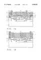
- FIG. 1ais a schematic cross-section of a fully packaged integrated circuit including a top layer of polymeric material that communicates to the chip level through extended via holes and a redistribution network.
- FIG. 1bis a schematic cross-section of a fully packaged integrated circuit including a top layer of polymeric material that communicates directly to the chip level through extended via holes.
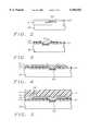
- FIG. 2shows parts of an integrated circuit prior to packaging.
- FIG. 3shows the structure of FIG. 2 after the addition of a planarizing layer that includes an access hole to the studs as well as a contacting layer.
- FIG. 4shows the structure of FIG. 3 following the addition of a redistribution layer.
- FIG. 5shows structure of FIG. 4 following the addition of a layer of polymetric material in which a via hole has been formed.
- FIG. 6is the structure seen in FIG. 5 after the via hole has been overfilled with metal to form a conducting post.
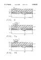
- FIG. 7ashows the structure of FIG. 6 following the formation of a solder ball at the end of a projecting post together with etchback to form a ⁇ lollipop ⁇ structure.
- FIG. 7bis like FIG. 7a except that a layer of UBM has been inserted between the solder ball and the polymeric layer.
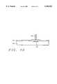
- FIG. 8shows the structure of FIG. 2 following the addition of a layer of polymetric material in which a via hole has been formed directly above the stud.
- FIG. 9is the structure seen in FIG. 8 after the via hole has been overfilled with metal to form a conducting post.
- FIG. 10ashows the structure of FIG. 9 following the formation of a solder ball at the end of a projecting post.
- FIG. 10bis like FIG. 10a except that a layer of UBM has been inserted between the solder ball and the polymeric layer.
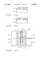
- FIGS. 11a and 11billustrate how the shape of a via hole formed in a photosensitive material may be modified depending on its properties and on the exposure mode used.
- FIG. 12shows how individual redistribution networks on chips may be connected together in the kerf to form a single common distribution network.
- FIG. 13shows a freestanding post which is to be almost covered by a layer of polymeric material.
- the present inventionteaches a process and a package for encapsulating an entire wafer with a layer of a polymeric material which is applied by any of several conventional techniques such as spin coating, dipping, spraying, or as a dry film and describes several low-cost ways of establishing electrical communication between terminals at the surface of the chip and solder bumps on the outer surface of the package.
- electroplatingis used to form parts of the package but it should be understood that electroless plating may be substituted for selected subprocesses without departing from the spirit of the invention.
- FIG. 1awe show a schematic representation of one embodiment.
- An integrated circuitis shown in cross-section as a series of layers that have been formed over silicon substrate 1.
- Successive layers 2, 3, and 4represent the device level and two levels of wiring respectively.
- Each layerhas been planarized.
- the top-level wiring, including I/O pads such as 6 and 7has been formed on the top surface of layer 4 and then covered by passivating layer 13 (usually silicon nitride) which in turn has been covered by a final planarizing layer 5 (typically, but not necessarily, of polyimide).
- passivating layer 13usually silicon nitride
- a final planarizing layer 5typically, but not necessarily, of polyimide.
- the pattern of studs 8will not coincide with the pattern of solder terminals on the card or board to which the chip is to be attached.
- BGAball grid array
- the chip manufacturing process for a standard flip chipwould normally terminate at this point.
- the processis continued with the application of a plastic (polymeric) layer 10 that gives the chip both environmental as well as mechanical protection.
- via holes 11, filled with a suitable conductive materialneed to be formed and fresh solder bumps 12 attached to their top ends.
- FIG. 1bis a schematic view of a second embodiment, representing a lower cost version of the package. It differs from FIG. 1a in that no redistribution network is present. This implies that the pattern of connecting studs is the same as the pattern of solder terminals on the next level package. This simplification allows final planarization layer 5 (in FIG. 1a) to be omitted from the structure. Instead, polymeric layer 15 is allowed to extend all the way down to passivating layer 13.
- polyimidessilicone elastomers
- benzocyclobuteneAll three types are readily applied by spin coating while in their uncured form and they may then be hardened (cured) through reaction with a hardening agent, usually, but not necessarily, accelerated by heating.
- the polyimidesare available in the form of dry films which can be applied directly to a surface by means of an adhesive. The choice of which material to use depends on a number of factors. These include:
- TCETemperature coefficient of expansion
- both Y and Ineed to be minimized.
- Ygold and solder are good choices although copper is to be preferred for other reasons, while I is proportional to the mass of the post, implying that a small diameter and low density are best.
- Integrated circuit 21is shown as having been formed over silicon substrate 20.
- Layer 22represents a passivating layer similar to layer 13 in FIGS. 1a and 1b, while connecting pad 23 (corresponding to stud 7 in FIG. 1a) is seen as being open to the outside world.
- layer 30represents everything in FIG. 2 below the pad 23, including layer 22.
- Layer 31 of polyimidehas been deposited by spin coating onto the surface of 30 and opening 32 has been formed in it using standard photolithographic techniques, including photosensitive polyimides. Layer 31 is generally between about 3 and 20 microns thick. This is followed by the deposition of layer 33 of chrome-copper generally but not necessarily, by sputtering, to a thickness that is between about 500 and 2,000 Angstroms.
- the individual chip-level distribution networksare connected to one another by using the otherwise empty space provided by the kerf, thereby forming a common distribution network as illustrated in FIG. 12 where individual redistribution networks in chip images 93-96 are seen to be connected together in the kerf regions 98 thereby forming a common distribution network one end of which is designated as 99.
- Electroplatingis then used to build up the thickness of the metal that forms the common distribution network. Electrical contact is made to metal layer 33 allowing metal to be plated in all areas not covered by the photoresist. For this metal we have preferred to use copper although metals such as aluminum could also have been used together with non-electroplating methods. At the completion of electroplating, resulting in an additional thickness of metal between about 0.5 and 5 microns thick, the photoresist is removed. An example of part of the redistribution network is shown as layer 41 in FIG. 4 and all parts of the contacting layer not covered by the redistribution network are selectively removed.
- a layer of polymeric materialis laid down. This is shown as layer 51 in FIG. 5. Its thickness is between about 20 and 250 microns.
- Via hole 52is then formed in it. This corresponds to via holes 11 in FIG. 1a.
- the polymeric materialis photosensitive.
- BCB and the polyimidesthere are many commercial compositions available for this.
- Via holes 52are then formed by exposing through a suitable mask and developing. By controlling the type of photosensitive materials as well as the exposure conditions, the shape of the via holes can be controlled. For example, if the photosensitive material generates a negative image of the mask this can cause the via holes to be wider closest to their bottom, i.e. closest to layer 41 as illustrated in FIG. 11a.
- the photosensitive materialgenerates a positive image of the mask and if an imaging system with a low depth of focus is used and if the image is focused in a plane midway between the two surfaces, the effect is for the via holes to be narrowest at a point halfway down the holes, as illustrated in FIG. 11b.
- the resulting conductive postswill have better strength and adhesion than conventional (simple cylindrical) posts.
- the polymeric materialis etched in the usual way using a photoresist mask. Since the photoresist and the polymeric material respond somewhat similarly to the etchants usually used for the latter, a hard mask (e.g. CVD silicon oxide) is often used.
- a hard maske.g. CVD silicon oxide
- the polymeric materialis etched using laser drilling.
- laser drillingFor polymeric layers thicker than about 100 microns this is the preferred method.
- An example of a laser well suited to this applicationis an eximer (209 nm) laser or a CO 2 (10.6 microns) laser with the capability of forming holes with diameters as low as about 50 microns.
- additional metalpreferably copper but other metals such as gold, solder (such as lead-tin), or aluminum (non-electroplated), could also have been used
- via hole 52was filled with metal, with post formation being continued past the point at which it was just filled.
- This projection of the post above the polymeric material surfaceis needed to anchor the solder bumps which are grown in the next step of the process.
- This ⁇ anchor ⁇ effectcan be further enhanced by etching back the polyimide material to some extent, as illustrated in FIG. 7a, to generate a ⁇ lollipop ⁇ structure for the post-bump combination.
- a solder bump such as 71is grown over the projecting tip of 67. Since electrical contact can still be made to 67 through the common distribution network, electroplating is the preferred method for accomplishing this. In general, electroplating offers better control, in particular control of the composition of the deposited layer, than is achievable by, for example, electroless plating.
- the extensions of the postsmay be first coated with a UBM layer 72 as shown in FIG. 7b prior to growing solder bump 71. This is done in the usual manner by first depositing over the entire surface and then patterning and etching.
- UBMUBM layer 72
- the advantage of providing this extra layer of UBMis that the base contact area for the solder balls is enlarged and hence their adhesion is increased. It would be used in cases where large solder balls are required. In both cases, the diameter of the solder bumps was between about 100 and 300 microns with a pitch that was typically between about 200 and 800 microns.
- solder bumps 71have been formed, the wafer is diced into individual chips by cutting along the kerf. In so doing the common distribution network is destroyed but each chip retains its own individual redistribution network.
- the processproceeds directly from the structure of FIG. 2 to the step of laying down a layer of polymeric material 80 (as illustrated in FIG. 8) whose thickness is between about 20 and 250 microns.
- via holes 82are formed in it with the added constraint that they are located directly above studs 23. These correspond to the via holes that will contain conductive posts 11 in FIG. 1b. In order to form these via holes, one of three subprocesses were used:
- the polymeric materialis photosensitive.
- the polymeric materialis photosensitive.
- polyimides or BCBthere are many commercial compositions available for this.
- Via holes 52are then formed by exposing through a suitable mask and developing. By controlling the type of photosensitive material as well as the exposure conditions, the shape of the via holes can be controlled. For example, if the photosensitive material generates a negative image of the mask this can cause the via holes to be wider closest to their bottom, i.e. closest to layer 41 as illustrated in FIG. 11a.
- the photosensitive materialgenerates a positive image of the mask and if an imaging system with a low depth of focus is used and if the image is focused in a plane midway between the two surfaces, the effect is for the via holes to be narrowest at a point halfway down the holes as illustrated in FIG. 11b.
- the polymeric materialis etched in the usual way using a photoresist mask. Since the photoresist and the polymeric material respond somewhat similarly to the etchants usually used for the latter, a hard mask (e.g. CVD silicon oxide) is often used .
- a hard maske.g. CVD silicon oxide
- the polymeric materialis etched using laser drilling.
- laser drillingFor polymeric layers thicker than about 100 microns this is the preferred method.
- An example of a laser well suited to this applicationis an eximer (209 nm) laser or a CO 2 (10.6 microns) laser with the capability of forming holes with diameters as low as about 50 microns.
- solder bump 81is grown over the projecting tip of 87. Since electrical contact cannot be made to 87, electroless plating has to be used.
- the extensions of the postsmay be first coated with a UBM layer 88 (as shown in FIG. 10b) prior to growing solder bump 81. This is done in the usual manner by first depositing over the entire surface and then patterning and etching.
- UBM layer 88as shown in FIG. 10b
- the advantage of providing this extra layer of UBMis that the base contact area for the solder balls is enlarged and hence their adhesion is increased. It would be used in cases where large solder balls are required. In both cases, the diameter of the solder bumps was between about 100 and 300 microns with a pitch that was typically between about 200 and 800 microns.
- solder bumpsinstead of forming the solder bumps through plating, they may be laid down by means of screen printing or stenciling. This is a viable approach for solder bumps having diameters in excess of about 100 microns with a pitch that is greater than about 200 microns.
- solder bumps 81have been formed, the wafer is diced into individual chips by cutting along the kerf.
- the preferred metal deposition methodis electroplating. Accordingly, a contacting metal layer is deposited over the entire passivation layer. See layer 45 in FIG. 13. This is followed by coating with a layer a photoresist in which via holes are formed in a similar manner to the formation of via holes in the photosensitive versions of the polymers as described in the first and second embodiments, including techniques for controlling the shapes of these via holes. The via holes are then filled with metal by means of electroplating following which the photoresist is stripped, leaving behind freestanding metal posts such as 46 in FIG. 13.
- the contacting layeris removed without any attack on the freestanding posts.
- the polymeric materialis applied to the wafer as a single layer whose thickness is less than the height of the freestanding posts, thereby allowing a certain amount of uncovered post material to project above the surface of the polymer.
- the structureis then completed as in the second embodiment through the formation of solder bumps by electroless plating, screen printing, or stenciling.
Landscapes
- Engineering & Computer Science (AREA)
- Computer Hardware Design (AREA)
- Microelectronics & Electronic Packaging (AREA)
- Power Engineering (AREA)
- Manufacturing & Machinery (AREA)
- Internal Circuitry In Semiconductor Integrated Circuit Devices (AREA)
Abstract
Description
TABLE I ______________________________________ PROPERTY POLYIMIDES ELASTOMERS BCB ______________________________________ Cure temperature 350° C. room temperature 250° C. Young's modulus 3.4 Gpa very small 2GPa Water absorption 3% low 0.2% TCE 40 × 10.sup.-6 /° C. 1 × 10.sup.-6 /° C. 52 × 10.sup.-6 /° C. Adhesion fair to good Good - excellent Fair to good ______________________________________
F=(3Yld)/L.sup.3, where Y=Young's modulus and I=moment of inertia
Claims (30)
Priority Applications (4)
| Application Number | Priority Date | Filing Date | Title |
|---|---|---|---|
| US09/131,429US6103552A (en) | 1998-08-10 | 1998-08-10 | Wafer scale packaging scheme |
| TW088111047ATW425645B (en) | 1998-08-10 | 1999-06-30 | Wafer scale packaging scheme |
| US09/617,012US6350705B1 (en) | 1998-08-10 | 2000-07-14 | Wafer scale packaging scheme |
| US09/619,017US6486563B1 (en) | 1998-08-10 | 2000-07-19 | Wafer scale packaging scheme |
Applications Claiming Priority (1)
| Application Number | Priority Date | Filing Date | Title |
|---|---|---|---|
| US09/131,429US6103552A (en) | 1998-08-10 | 1998-08-10 | Wafer scale packaging scheme |
Related Child Applications (2)
| Application Number | Title | Priority Date | Filing Date |
|---|---|---|---|
| US09/617,012Continuation-In-PartUS6350705B1 (en) | 1998-08-10 | 2000-07-14 | Wafer scale packaging scheme |
| US09/619,017DivisionUS6486563B1 (en) | 1998-08-10 | 2000-07-19 | Wafer scale packaging scheme |
Publications (1)
| Publication Number | Publication Date |
|---|---|
| US6103552Atrue US6103552A (en) | 2000-08-15 |
Family
ID=22449427
Family Applications (3)
| Application Number | Title | Priority Date | Filing Date |
|---|---|---|---|
| US09/131,429Expired - LifetimeUS6103552A (en) | 1998-08-10 | 1998-08-10 | Wafer scale packaging scheme |
| US09/617,012Expired - LifetimeUS6350705B1 (en) | 1998-08-10 | 2000-07-14 | Wafer scale packaging scheme |
| US09/619,017Expired - LifetimeUS6486563B1 (en) | 1998-08-10 | 2000-07-19 | Wafer scale packaging scheme |
Family Applications After (2)
| Application Number | Title | Priority Date | Filing Date |
|---|---|---|---|
| US09/617,012Expired - LifetimeUS6350705B1 (en) | 1998-08-10 | 2000-07-14 | Wafer scale packaging scheme |
| US09/619,017Expired - LifetimeUS6486563B1 (en) | 1998-08-10 | 2000-07-19 | Wafer scale packaging scheme |
Country Status (2)
| Country | Link |
|---|---|
| US (3) | US6103552A (en) |
| TW (1) | TW425645B (en) |
Cited By (157)
| Publication number | Priority date | Publication date | Assignee | Title |
|---|---|---|---|---|
| US6316830B1 (en) | 1998-12-17 | 2001-11-13 | Charles Wen Chyang Lin | Bumpless flip chip assembly with strips and via-fill |
| US6350633B1 (en)* | 2000-08-22 | 2002-02-26 | Charles W. C. Lin | Semiconductor chip assembly with simultaneously electroplated contact terminal and connection joint |
| US6350632B1 (en) | 2000-09-20 | 2002-02-26 | Charles W. C. Lin | Semiconductor chip assembly with ball bond connection joint |
| US6350386B1 (en) | 2000-09-20 | 2002-02-26 | Charles W. C. Lin | Method of making a support circuit with a tapered through-hole for a semiconductor chip assembly |
| US6372545B1 (en) | 2001-03-22 | 2002-04-16 | Taiwan Semiconductor Manufacturing Company | Method for under bump metal patterning of bumping process |
| US6403400B2 (en) | 1998-12-17 | 2002-06-11 | Charles Wen Chyang Lin | Bumpless flip chip assembly with strips-in-via and plating |
| US6403460B1 (en) | 2000-08-22 | 2002-06-11 | Charles W. C. Lin | Method of making a semiconductor chip assembly |
| US6402970B1 (en) | 2000-08-22 | 2002-06-11 | Charles W. C. Lin | Method of making a support circuit for a semiconductor chip assembly |
| US6406939B1 (en) | 1998-05-02 | 2002-06-18 | Charles W. C. Lin | Flip chip assembly with via interconnection |
| US6410414B1 (en)* | 1998-12-28 | 2002-06-25 | Samsung Electronics Co., Ltd. | Method for fabricating a semiconductor device |
| US20020093082A1 (en)* | 2001-01-18 | 2002-07-18 | Toshio Miyamoto | Semiconductor device and manufacturing method of that |
| US6436734B1 (en) | 2000-08-22 | 2002-08-20 | Charles W. C. Lin | Method of making a support circuit for a semiconductor chip assembly |
| US6440835B1 (en) | 2000-10-13 | 2002-08-27 | Charles W. C. Lin | Method of connecting a conductive trace to a semiconductor chip |
| US6444489B1 (en) | 2000-12-15 | 2002-09-03 | Charles W. C. Lin | Semiconductor chip assembly with bumped molded substrate |
| US6448644B1 (en)* | 1998-05-02 | 2002-09-10 | Charles W. C. Lin | Flip chip assembly with via interconnection |
| US6448108B1 (en) | 2000-10-02 | 2002-09-10 | Charles W. C. Lin | Method of making a semiconductor chip assembly with a conductive trace subtractively formed before and after chip attachment |
| US6479900B1 (en)* | 1998-12-22 | 2002-11-12 | Sanyo Electric Co., Ltd. | Semiconductor device and method of manufacturing the same |
| US6492252B1 (en) | 2000-10-13 | 2002-12-10 | Bridge Semiconductor Corporation | Method of connecting a bumped conductive trace to a semiconductor chip |
| WO2002101829A1 (en)* | 2001-06-13 | 2002-12-19 | Advanpack Solutions Pte Ltd | Method for forming a wafer level chip scale package, and package formed thereby |
| WO2002067292A3 (en)* | 2001-02-20 | 2002-12-19 | Dow Corning | Semiconductor package and method of preparing same |
| US20020195673A1 (en)* | 2001-06-08 | 2002-12-26 | Chou Tsung-Kuan A. | Low-temperature patterned wafer bonding with photosensitive benzocyclobutene (BCB) and 3D MEMS (microelectromechanical systems) structure fabrication |
| US6511865B1 (en) | 2000-09-20 | 2003-01-28 | Charles W. C. Lin | Method for forming a ball bond connection joint on a conductive trace and conductive pad in a semiconductor chip assembly |
| US6528891B2 (en) | 1998-12-17 | 2003-03-04 | Charles Wen Chyang Lin | Bumpless flip chip assembly with solder via |
| US6537851B1 (en) | 2000-10-13 | 2003-03-25 | Bridge Semiconductor Corporation | Method of connecting a bumped compliant conductive trace to a semiconductor chip |
| US6544813B1 (en) | 2000-10-02 | 2003-04-08 | Charles W. C. Lin | Method of making a semiconductor chip assembly with a conductive trace subtractively formed before and after chip attachment |
| US6548393B1 (en) | 2000-10-13 | 2003-04-15 | Charles W. C. Lin | Semiconductor chip assembly with hardened connection joint |
| US6551861B1 (en) | 2000-08-22 | 2003-04-22 | Charles W. C. Lin | Method of making a semiconductor chip assembly by joining the chip to a support circuit with an adhesive |
| US6557225B2 (en)* | 2000-04-13 | 2003-05-06 | Murata Manufacturing Co., Ltd. | Method of producing surface acoustic wave device |
| US6562657B1 (en) | 2000-08-22 | 2003-05-13 | Charles W. C. Lin | Semiconductor chip assembly with simultaneously electrolessly plated contact terminal and connection joint |
| US6562709B1 (en)* | 2000-08-22 | 2003-05-13 | Charles W. C. Lin | Semiconductor chip assembly with simultaneously electroplated contact terminal and connection joint |
| US6576493B1 (en) | 2000-10-13 | 2003-06-10 | Bridge Semiconductor Corporation | Method of connecting a conductive trace and an insulative base to a semiconductor chip using multiple etch steps |
| US6576539B1 (en) | 2000-10-13 | 2003-06-10 | Charles W.C. Lin | Semiconductor chip assembly with interlocked conductive trace |
| US6583040B1 (en) | 2000-10-13 | 2003-06-24 | Bridge Semiconductor Corporation | Method of making a pillar in a laminated structure for a semiconductor chip assembly |
| US6605525B2 (en)* | 2001-05-01 | 2003-08-12 | Industrial Technologies Research Institute | Method for forming a wafer level package incorporating a multiplicity of elastomeric blocks and package formed |
| US20030160335A1 (en)* | 2002-02-27 | 2003-08-28 | Ho-Ming Tong | Flip chip interconnection structure and fabrication process thereof |
| US6630359B1 (en)* | 1998-07-31 | 2003-10-07 | Commissariat A L'energie Atomique | Micro-system with multiple points for chemical or biological analysis |
| US20030211720A1 (en)* | 2002-05-13 | 2003-11-13 | Taiwan Semiconductor Manufacturing Co., Ltd. | Method of wafer level chip scale packaging |
| US6653170B1 (en) | 2001-02-06 | 2003-11-25 | Charles W. C. Lin | Semiconductor chip assembly with elongated wire ball bonded to chip and electrolessly plated to support circuit |
| US6660626B1 (en) | 2000-08-22 | 2003-12-09 | Charles W. C. Lin | Semiconductor chip assembly with simultaneously electrolessly plated contact terminal and connection joint |
| US6667229B1 (en) | 2000-10-13 | 2003-12-23 | Bridge Semiconductor Corporation | Method of connecting a bumped compliant conductive trace and an insulative base to a semiconductor chip |
| US6674162B2 (en)* | 2000-03-30 | 2004-01-06 | Sanyo Electric Co., Ltd. | Semiconductor device and manufacturing method thereof |
| US6699780B1 (en) | 2000-10-13 | 2004-03-02 | Bridge Semiconductor Corporation | Method of connecting a conductive trace to a semiconductor chip using plasma undercut etching |
| US6740576B1 (en) | 2000-10-13 | 2004-05-25 | Bridge Semiconductor Corporation | Method of making a contact terminal with a plated metal peripheral sidewall portion for a semiconductor chip assembly |
| US20040104486A1 (en)* | 2000-02-16 | 2004-06-03 | Micron Technology, Inc. | Electronic apparatus having an adhesive layer from wafer level packaging |
| US20040198022A1 (en)* | 2001-04-26 | 2004-10-07 | Advanpack Solutions Pte. Ltd. | Method for forming a wafer level chip scale package, and package formed thereby |
| US20040205565A1 (en)* | 2001-10-23 | 2004-10-14 | Sun Microsystems, Inc. | XML based report generator |
| US6818545B2 (en) | 2001-03-05 | 2004-11-16 | Megic Corporation | Low fabrication cost, fine pitch and high reliability solder bump |
| US20040245608A1 (en)* | 2003-06-09 | 2004-12-09 | Siliconware Precision Industries Co., Ltd. | Semiconductor package having conductive bumps on chip and method for fabricating the same |
| US20050064624A1 (en)* | 2003-09-18 | 2005-03-24 | Minami Co., Ltd. | Method of manufacturing wafer level chip size package |
| US6872591B1 (en) | 2000-10-13 | 2005-03-29 | Bridge Semiconductor Corporation | Method of making a semiconductor chip assembly with a conductive trace and a substrate |
| US6876072B1 (en) | 2000-10-13 | 2005-04-05 | Bridge Semiconductor Corporation | Semiconductor chip assembly with chip in substrate cavity |
| US20050104177A1 (en)* | 2000-10-18 | 2005-05-19 | Megic Corporation | Post passivation interconnection schemes on top of the IC chips |
| US6908788B1 (en) | 2000-10-13 | 2005-06-21 | Bridge Semiconductor Corporation | Method of connecting a conductive trace to a semiconductor chip using a metal base |
| US20050189650A1 (en)* | 2001-09-17 | 2005-09-01 | Megic Corporation | Low fabrication cost, high performance, high reliability chip scale package |
| US6940177B2 (en) | 2002-05-16 | 2005-09-06 | Dow Corning Corporation | Semiconductor package and method of preparing same |
| US6949408B1 (en) | 2000-10-13 | 2005-09-27 | Bridge Semiconductor Corporation | Method of connecting a conductive trace and an insulative base to a semiconductor chip using multiple etch steps |
| US20050242418A1 (en)* | 2004-04-30 | 2005-11-03 | Wen-Kun Yang | Structure of package |
| US6984576B1 (en) | 2000-10-13 | 2006-01-10 | Bridge Semiconductor Corporation | Method of connecting an additively and subtractively formed conductive trace and an insulative base to a semiconductor chip |
| US20060014316A1 (en)* | 2000-10-13 | 2006-01-19 | Bridge Semiconductor Corporation | Method of making a semiconductor chip assemby with a metal containment wall and a solder terminal |
| USRE38961E1 (en)* | 1998-10-06 | 2006-01-31 | Casio Computer Co., Ltd. | Method for production of semiconductor package |
| US20060022311A1 (en)* | 2003-05-08 | 2006-02-02 | Mou-Shiung Lin | Chip structure with redistribution Circuit, chip package and manufacturing process thereof |
| US7009297B1 (en) | 2000-10-13 | 2006-03-07 | Bridge Semiconductor Corporation | Semiconductor chip assembly with embedded metal particle |
| US20060063378A1 (en)* | 2004-09-23 | 2006-03-23 | Megie Corporation | Top layers of metal for integrated circuits |
| US20060138671A1 (en)* | 2004-12-24 | 2006-06-29 | Kiyonori Watanabe | Semiconductor device and fabrication method thereof |
| US7071089B1 (en) | 2000-10-13 | 2006-07-04 | Bridge Semiconductor Corporation | Method of making a semiconductor chip assembly with a carved bumped terminal |
| US7075186B1 (en) | 2000-10-13 | 2006-07-11 | Bridge Semiconductor Corporation | Semiconductor chip assembly with interlocked contact terminal |
| US7094676B1 (en) | 2000-10-13 | 2006-08-22 | Bridge Semiconductor Corporation | Semiconductor chip assembly with embedded metal pillar |
| US7112521B1 (en) | 2000-10-13 | 2006-09-26 | Bridge Semiconductor Corporation | Method of making a semiconductor chip assembly with a bumped metal pillar |
| US7129113B1 (en) | 2000-10-13 | 2006-10-31 | Bridge Semiconductor Corporation | Method of making a three-dimensional stacked semiconductor package with a metal pillar in an encapsulant aperture |
| US7132741B1 (en) | 2000-10-13 | 2006-11-07 | Bridge Semiconductor Corporation | Semiconductor chip assembly with carved bumped terminal |
| US20060279003A1 (en)* | 1999-11-11 | 2006-12-14 | Fujitsu Limited | Semiconductor device having an alignment mark formed by the same material with a metal post |
| US20070007659A1 (en)* | 2003-11-19 | 2007-01-11 | Chandrasekhar Narayan | Seedless wirebond pad plating |
| US20070015357A1 (en)* | 2005-07-15 | 2007-01-18 | Government Of The Usa, As Represented By Secretary Of U.S. Army | Process of adhesive bonding with patternable polymers for producing microstructure devices on a wafer assembly |
| US7190080B1 (en) | 2000-10-13 | 2007-03-13 | Bridge Semiconductor Corporation | Semiconductor chip assembly with embedded metal pillar |
| US20070057367A1 (en)* | 2001-07-10 | 2007-03-15 | Samsung Electronics Co., Ltd. | Semiconductor chip having bond pads and multi-chip package |
| US7262082B1 (en) | 2000-10-13 | 2007-08-28 | Bridge Semiconductor Corporation | Method of making a three-dimensional stacked semiconductor package with a metal pillar and a conductive interconnect in an encapsulant aperture |
| US20070200244A1 (en)* | 2003-10-15 | 2007-08-30 | Mou-Shiung Lin | Post passivation interconnection schemes on top of the IC chips |
| US7264991B1 (en) | 2000-10-13 | 2007-09-04 | Bridge Semiconductor Corporation | Method of connecting a conductive trace to a semiconductor chip using conductive adhesive |
| US7268421B1 (en) | 2004-11-10 | 2007-09-11 | Bridge Semiconductor Corporation | Semiconductor chip assembly with welded metal pillar that includes enlarged ball bond |
| US7271489B2 (en) | 2003-10-15 | 2007-09-18 | Megica Corporation | Post passivation interconnection schemes on top of the IC chips |
| US20070224779A1 (en)* | 2006-03-23 | 2007-09-27 | Park Soo G | Method for fabricating a BGA device and BGA device |
| US20070273032A1 (en)* | 1998-12-21 | 2007-11-29 | Mou-Shiung Lin | Top layers of metal for high performance IC's |
| US20080001244A1 (en)* | 2004-02-26 | 2008-01-03 | Herbert Schwarzbauer | System Comprising an Electrical Component and an Electrical Connecting Lead for Said Component, and Method for the Production of Said System |
| US7319265B1 (en) | 2000-10-13 | 2008-01-15 | Bridge Semiconductor Corporation | Semiconductor chip assembly with precision-formed metal pillar |
| US20080029819A1 (en)* | 2006-08-04 | 2008-02-07 | Seiko Epson Corporation | Semiconductor device |
| US20080067677A1 (en)* | 2001-03-05 | 2008-03-20 | Megica Corporation | Structure and manufacturing method of a chip scale package |
| US20080083976A1 (en)* | 2006-10-10 | 2008-04-10 | Tessera, Inc. | Edge connect wafer level stacking |
| US20080083977A1 (en)* | 2006-10-10 | 2008-04-10 | Tessera, Inc. | Edge connect wafer level stacking |
| US20080113504A1 (en)* | 2002-05-01 | 2008-05-15 | Megica Corporation | Low fabrication cost, high performance, high reliability chip scale package |
| US20080116545A1 (en)* | 2006-11-22 | 2008-05-22 | Tessera, Inc. | Packaged semiconductor chips |
| US20080116544A1 (en)* | 2006-11-22 | 2008-05-22 | Tessera, Inc. | Packaged semiconductor chips with array |
| US20080138935A1 (en)* | 2006-12-12 | 2008-06-12 | Siliconware Precision Industries Co., Ltd. | Chip scale package structure and method for fabricating the same |
| US20080157323A1 (en)* | 2006-12-28 | 2008-07-03 | Tessera, Inc. | Stacked packages |
| US7396703B1 (en) | 2003-11-20 | 2008-07-08 | Bridge Semiconductor Corporation | Method of making a semiconductor chip assembly with a bumped terminal and a filler |
| US20080171413A1 (en)* | 2007-01-17 | 2008-07-17 | International Business Machines Corporation | Method of Reducing Detrimental STI-Induced Stress in MOSFET Channels |
| US7405149B1 (en) | 1998-12-21 | 2008-07-29 | Megica Corporation | Post passivation method for semiconductor chip or wafer |
| US20080246136A1 (en)* | 2007-03-05 | 2008-10-09 | Tessera, Inc. | Chips having rear contacts connected by through vias to front contacts |
| US20080265413A1 (en)* | 2005-10-28 | 2008-10-30 | Megica Corporation | Semiconductor chip with post-passivation scheme formed over passivation layer |
| US7446419B1 (en) | 2004-11-10 | 2008-11-04 | Bridge Semiconductor Corporation | Semiconductor chip assembly with welded metal pillar of stacked metal balls |
| US20090039528A1 (en)* | 2007-08-09 | 2009-02-12 | Tessera, Inc. | Wafer level stacked packages with individual chip selection |
| US7494843B1 (en) | 2006-12-26 | 2009-02-24 | Bridge Semiconductor Corporation | Method of making a semiconductor chip assembly with thermal conductor and encapsulant grinding |
| US20090057895A1 (en)* | 2005-05-06 | 2009-03-05 | Megica Corporation | Post passivation structure for a semiconductor device and packaging process for same |
| US20090065907A1 (en)* | 2007-07-31 | 2009-03-12 | Tessera, Inc. | Semiconductor packaging process using through silicon vias |
| US7538415B1 (en) | 2003-11-20 | 2009-05-26 | Bridge Semiconductor Corporation | Semiconductor chip assembly with bumped terminal, filler and insulative base |
| US20090146305A1 (en)* | 2004-10-12 | 2009-06-11 | Megica Corporation | Post passivation interconnection schemes on top of the ic chips |
| US20090160065A1 (en)* | 2006-10-10 | 2009-06-25 | Tessera, Inc. | Reconstituted Wafer Level Stacking |
| US20090174045A1 (en)* | 2008-01-03 | 2009-07-09 | International Business Machines Corporation | Bump Pad Metallurgy Employing An Electrolytic Cu / Electorlytic Ni / Electrolytic Cu Stack |
| US20090212381A1 (en)* | 2008-02-26 | 2009-08-27 | Tessera, Inc. | Wafer level packages for rear-face illuminated solid state image sensors |
| US20090316378A1 (en)* | 2008-06-16 | 2009-12-24 | Tessera Research Llc | Wafer level edge stacking |
| US20100053407A1 (en)* | 2008-02-26 | 2010-03-04 | Tessera, Inc. | Wafer level compliant packages for rear-face illuminated solid state image sensors |
| US20100136715A1 (en)* | 2006-07-28 | 2010-06-03 | Midwest Research Institute | Screening of Silicon Wafers Used in Photovoltaics |
| US7750483B1 (en)* | 2004-11-10 | 2010-07-06 | Bridge Semiconductor Corporation | Semiconductor chip assembly with welded metal pillar and enlarged plated contact terminal |
| US20100219527A1 (en)* | 2009-02-27 | 2010-09-02 | Frank Feustel | Metallization system of a semiconductor device including metal pillars having a reduced diameter at the bottom |
| US20100230795A1 (en)* | 2009-03-13 | 2010-09-16 | Tessera Technologies Hungary Kft. | Stacked microelectronic assemblies having vias extending through bond pads |
| US7811863B1 (en) | 2006-10-26 | 2010-10-12 | Bridge Semiconductor Corporation | Method of making a semiconductor chip assembly with metal pillar and encapsulant grinding and heat sink attachment |
| US20100270679A1 (en)* | 2006-10-17 | 2010-10-28 | Tessera, Inc. | Microelectronic packages fabricated at the wafer level and methods therefor |
| US20110001234A1 (en)* | 2009-07-06 | 2011-01-06 | Oki Semiconductor Co., Ltd. | Semiconductor device and fabrication method thereof |
| US20110006432A1 (en)* | 2007-07-27 | 2011-01-13 | Tessera, Inc. | Reconstituted wafer stack packaging with after-applied pad extensions |
| US7993983B1 (en) | 2003-11-17 | 2011-08-09 | Bridge Semiconductor Corporation | Method of making a semiconductor chip assembly with chip and encapsulant grinding |
| US20110227219A1 (en)* | 2010-03-17 | 2011-09-22 | Maxim Integrated Products, Inc. | Enhanced wlp for superior temp cycling, drop test and high current applications |
| US20120086123A1 (en)* | 2010-10-06 | 2012-04-12 | Samsung Electronics Co., Ltd. | Semiconductor assembly and semiconductor package including a solder channel |
| US20120155055A1 (en)* | 2010-12-21 | 2012-06-21 | Tessera, Inc. | Semiconductor chip assembly and method for making same |
| US8242601B2 (en) | 2004-10-29 | 2012-08-14 | Megica Corporation | Semiconductor chip with passivation layer comprising metal interconnect and contact pads |
| USRE43674E1 (en) | 2000-10-18 | 2012-09-18 | Megica Corporation | Post passivation metal scheme for high-performance integrated circuit devices |
| US20120252168A1 (en)* | 2011-04-01 | 2012-10-04 | International Business Machines Corporation | Copper Post Solder Bumps on Substrate |
| US20120313243A1 (en)* | 2011-06-13 | 2012-12-13 | Siliconware Precision Industries Co., Ltd. | Chip-scale package |
| US8334174B2 (en) | 2010-07-26 | 2012-12-18 | Siliconware Precision Industries Co., Ltd. | Chip scale package and fabrication method thereof |
| US8432045B2 (en) | 2010-11-15 | 2013-04-30 | Tessera, Inc. | Conductive pads defined by embedded traces |
| US20130127045A1 (en)* | 2011-11-22 | 2013-05-23 | Taiwan Semiconductor Manufacturing Company, Ltd. | Mechanisms for forming fine-pitch copper bump structures |
| US8525348B2 (en) | 2010-08-04 | 2013-09-03 | Siliconware Precision Industries Co., Ltd. | Chip scale package and fabrication method thereof |
| US20130256840A1 (en)* | 2010-04-30 | 2013-10-03 | Stats Chippac, Ltd. | Semiconductor Device and Method of Forming Protective Coating Material Over Semiconductor Wafer to Reduce Lamination Tape Residue |
| US8551815B2 (en) | 2007-08-03 | 2013-10-08 | Tessera, Inc. | Stack packages using reconstituted wafers |
| US8587126B2 (en) | 2010-12-02 | 2013-11-19 | Tessera, Inc. | Stacked microelectronic assembly with TSVs formed in stages with plural active chips |
| US8598465B2 (en) | 2011-01-27 | 2013-12-03 | Northrop Grumman Systems Corporation | Hermetic circuit ring for BCB WSA circuits |
| US8610264B2 (en) | 2010-12-08 | 2013-12-17 | Tessera, Inc. | Compliant interconnects in wafers |
| US8610259B2 (en) | 2010-09-17 | 2013-12-17 | Tessera, Inc. | Multi-function and shielded 3D interconnects |
| US8637968B2 (en) | 2010-12-02 | 2014-01-28 | Tessera, Inc. | Stacked microelectronic assembly having interposer connecting active chips |
| US8736066B2 (en) | 2010-12-02 | 2014-05-27 | Tessera, Inc. | Stacked microelectronic assemby with TSVS formed in stages and carrier above chip |
| US8780343B2 (en) | 2006-07-28 | 2014-07-15 | Alliance For Sustainable Energy, Llc | Wafer screening device and methods for wafer screening |
| US8791575B2 (en) | 2010-07-23 | 2014-07-29 | Tessera, Inc. | Microelectronic elements having metallic pads overlying vias |
| US8796135B2 (en) | 2010-07-23 | 2014-08-05 | Tessera, Inc. | Microelectronic elements with rear contacts connected with via first or via middle structures |
| US8847380B2 (en) | 2010-09-17 | 2014-09-30 | Tessera, Inc. | Staged via formation from both sides of chip |
| US8872336B2 (en) | 2011-11-18 | 2014-10-28 | Chipmos Technologies Inc. | Conductive structure and method for forming the same |
| US8884433B2 (en) | 2005-06-24 | 2014-11-11 | Qualcomm Incorporated | Circuitry component and method for forming the same |
| US20150123264A1 (en)* | 2013-11-01 | 2015-05-07 | Infineon Technologies Ag | Semiconductor Devices and Methods of Forming Thereof |
| US20150137350A1 (en)* | 2013-11-18 | 2015-05-21 | Taiwan Semiconductor Manufacturing Company Ltd. | Semiconductor device and fabricating method thereof |
| US9040361B2 (en) | 2010-08-12 | 2015-05-26 | Siliconware Precision Industries Co., Ltd. | Chip scale package with electronic component received in encapsulant, and fabrication method thereof |
| US9245862B1 (en)* | 2013-02-12 | 2016-01-26 | Amkor Technology, Inc. | Electronic component package fabrication method and structure |
| US9570342B1 (en) | 2014-01-17 | 2017-02-14 | Altera Corporation | Via structure and method for its fabrication |
| US9640437B2 (en) | 2010-07-23 | 2017-05-02 | Tessera, Inc. | Methods of forming semiconductor elements using micro-abrasive particle stream |
| US9704818B1 (en) | 2016-07-06 | 2017-07-11 | Nanya Technology Corporation | Semiconductor structure and manufacturing method thereof |
| US20180114763A1 (en)* | 2016-08-05 | 2018-04-26 | Nanya Technology Corporation | Method for manufacturing a semiconductor structure |
| US20180218953A1 (en)* | 2016-04-28 | 2018-08-02 | Taiwan Semiconductor Manufacturing Co., Ltd. | Semiconductor structure with conductive structure |
| US10103114B2 (en) | 2016-09-21 | 2018-10-16 | Nanya Technology Corporation | Semiconductor structure and manufacturing method thereof |
| US10134670B2 (en)* | 2015-04-08 | 2018-11-20 | International Business Machines Corporation | Wafer with plated wires and method of fabricating same |
| US20200020548A1 (en)* | 2012-12-28 | 2020-01-16 | Taiwan Semiconductor Manufacturing Company, Ltd. | Post-passivation interconnect structure and method of forming the same |
| US11094659B2 (en)* | 2019-09-30 | 2021-08-17 | Texas Instruments Incorporated | Microelectronic device with pillars having flared ends |
Families Citing this family (17)
| Publication number | Priority date | Publication date | Assignee | Title |
|---|---|---|---|---|
| US6803667B2 (en)* | 2001-08-09 | 2004-10-12 | Denso Corporation | Semiconductor device having a protective film |
| US7205649B2 (en)* | 2003-06-30 | 2007-04-17 | Intel Corporation | Ball grid array copper balancing |
| US7402908B2 (en) | 2005-05-05 | 2008-07-22 | Micron Technology, Inc. | Intermediate semiconductor device structures |
| US8319343B2 (en)* | 2005-09-21 | 2012-11-27 | Agere Systems Llc | Routing under bond pad for the replacement of an interconnect layer |
| US7952206B2 (en)* | 2005-09-27 | 2011-05-31 | Agere Systems Inc. | Solder bump structure for flip chip semiconductor devices and method of manufacture therefore |
| US8552560B2 (en)* | 2005-11-18 | 2013-10-08 | Lsi Corporation | Alternate pad structures/passivation inegration schemes to reduce or eliminate IMC cracking in post wire bonded dies during Cu/Low-K BEOL processing |
| US7888257B2 (en)* | 2007-10-10 | 2011-02-15 | Agere Systems Inc. | Integrated circuit package including wire bonds |
| JP2011502352A (en)* | 2007-10-31 | 2011-01-20 | アギア システムズ インコーポレーテッド | Bond pad support structure for semiconductor devices |
| TWI364804B (en)* | 2007-11-14 | 2012-05-21 | Ind Tech Res Inst | Wafer level sensor package structure and method therefor |
| US8072071B2 (en)* | 2009-02-19 | 2011-12-06 | Infineon Technologies Ag | Semiconductor device including conductive element |
| TWI445147B (en)* | 2009-10-14 | 2014-07-11 | Advanced Semiconductor Eng | Semiconductor device |
| TW201113962A (en)* | 2009-10-14 | 2011-04-16 | Advanced Semiconductor Eng | Chip having metal pillar structure |
| US8294265B1 (en) | 2010-03-31 | 2012-10-23 | Amkor Technology, Inc. | Semiconductor device for improving electrical and mechanical connectivity of conductive pillers and method therefor |
| TWI478303B (en) | 2010-09-27 | 2015-03-21 | Advanced Semiconductor Eng | Chip having metal pillar and package having the same |
| TWI451546B (en) | 2010-10-29 | 2014-09-01 | Advanced Semiconductor Eng | Stacked semiconductor package, semiconductor package thereof and method for making a semiconductor package |
| US8884443B2 (en) | 2012-07-05 | 2014-11-11 | Advanced Semiconductor Engineering, Inc. | Substrate for semiconductor package and process for manufacturing |
| US8686568B2 (en) | 2012-09-27 | 2014-04-01 | Advanced Semiconductor Engineering, Inc. | Semiconductor package substrates having layered circuit segments, and related methods |
Citations (9)
| Publication number | Priority date | Publication date | Assignee | Title |
|---|---|---|---|---|
| US5239191A (en)* | 1990-01-19 | 1993-08-24 | Kabushiki Kaisha Toshiba | Semiconductor wafer |
| US5514613A (en)* | 1994-01-27 | 1996-05-07 | Integrated Device Technology | Parallel manufacturing of semiconductor devices and the resulting structure |
| US5530418A (en)* | 1995-07-26 | 1996-06-25 | Taiwan Semiconductor Manufacturing Company | Method for shielding polysilicon resistors from hydrogen intrusion |
| US5731222A (en)* | 1995-08-01 | 1998-03-24 | Hughes Aircraft Company | Externally connected thin electronic circuit having recessed bonding pads |
| US5837557A (en)* | 1997-03-14 | 1998-11-17 | Advanced Micro Devices, Inc. | Semiconductor fabrication method of forming a master layer to combine individually printed blocks of a circuit pattern |
| US5851911A (en)* | 1996-03-07 | 1998-12-22 | Micron Technology, Inc. | Mask repattern process |
| US5897337A (en)* | 1994-09-30 | 1999-04-27 | Nec Corporation | Process for adhesively bonding a semiconductor chip to a carrier film |
| US5958800A (en)* | 1996-10-07 | 1999-09-28 | Taiwan Semiconductor Manufacturing Company, Ltd. | Method for post planarization metal photolithography |
| US5994783A (en)* | 1996-09-11 | 1999-11-30 | Lg Semicon Co., Ltd. | Semiconductor chip package and fabrication method thereof |
Family Cites Families (5)
| Publication number | Priority date | Publication date | Assignee | Title |
|---|---|---|---|---|
| US5418687A (en)* | 1994-02-01 | 1995-05-23 | Hewlett-Packard Company | Wafer scale multi-chip module |
| US6028364A (en)* | 1994-09-20 | 2000-02-22 | Hitachi, Ltd. | Semiconductor device having a stress relieving mechanism |
| US6080605A (en)* | 1998-10-06 | 2000-06-27 | Tessera, Inc. | Methods of encapsulating a semiconductor chip using a settable encapsulant |
| JPH11148068A (en)* | 1997-11-18 | 1999-06-02 | Shinko Electric Ind Co Ltd | Anisotropic stress buffer and semiconductor device by using the same |
| US6197613B1 (en)* | 1999-03-23 | 2001-03-06 | Industrial Technology Research Institute | Wafer level packaging method and devices formed |
- 1998
- 1998-08-10USUS09/131,429patent/US6103552A/ennot_activeExpired - Lifetime
- 1999
- 1999-06-30TWTW088111047Apatent/TW425645B/ennot_activeIP Right Cessation
- 2000
- 2000-07-14USUS09/617,012patent/US6350705B1/ennot_activeExpired - Lifetime
- 2000-07-19USUS09/619,017patent/US6486563B1/ennot_activeExpired - Lifetime
Patent Citations (9)
| Publication number | Priority date | Publication date | Assignee | Title |
|---|---|---|---|---|
| US5239191A (en)* | 1990-01-19 | 1993-08-24 | Kabushiki Kaisha Toshiba | Semiconductor wafer |
| US5514613A (en)* | 1994-01-27 | 1996-05-07 | Integrated Device Technology | Parallel manufacturing of semiconductor devices and the resulting structure |
| US5897337A (en)* | 1994-09-30 | 1999-04-27 | Nec Corporation | Process for adhesively bonding a semiconductor chip to a carrier film |
| US5530418A (en)* | 1995-07-26 | 1996-06-25 | Taiwan Semiconductor Manufacturing Company | Method for shielding polysilicon resistors from hydrogen intrusion |
| US5731222A (en)* | 1995-08-01 | 1998-03-24 | Hughes Aircraft Company | Externally connected thin electronic circuit having recessed bonding pads |
| US5851911A (en)* | 1996-03-07 | 1998-12-22 | Micron Technology, Inc. | Mask repattern process |
| US5994783A (en)* | 1996-09-11 | 1999-11-30 | Lg Semicon Co., Ltd. | Semiconductor chip package and fabrication method thereof |
| US5958800A (en)* | 1996-10-07 | 1999-09-28 | Taiwan Semiconductor Manufacturing Company, Ltd. | Method for post planarization metal photolithography |
| US5837557A (en)* | 1997-03-14 | 1998-11-17 | Advanced Micro Devices, Inc. | Semiconductor fabrication method of forming a master layer to combine individually printed blocks of a circuit pattern |
Non-Patent Citations (2)
| Title |
|---|
| M. Hou, "Wafer level packaging for CSPS" Semiconductor International, Jul. 1998, p. 305-308. |
| M. Hou, Wafer level packaging for CSPS Semiconductor International, Jul. 1998, p. 305 308.* |
Cited By (361)
| Publication number | Priority date | Publication date | Assignee | Title |
|---|---|---|---|---|
| US20050215043A1 (en)* | 1998-03-31 | 2005-09-29 | Megic Corporation | Low fabrication cost, high performance, high reliability chip scale package |
| US7338890B2 (en)* | 1998-03-31 | 2008-03-04 | Megica Corporation | Low fabrication cost, high performance, high reliability chip scale package |
| US6406939B1 (en) | 1998-05-02 | 2002-06-18 | Charles W. C. Lin | Flip chip assembly with via interconnection |
| US6448644B1 (en)* | 1998-05-02 | 2002-09-10 | Charles W. C. Lin | Flip chip assembly with via interconnection |
| US6630359B1 (en)* | 1998-07-31 | 2003-10-07 | Commissariat A L'energie Atomique | Micro-system with multiple points for chemical or biological analysis |
| USRE38961E1 (en)* | 1998-10-06 | 2006-01-31 | Casio Computer Co., Ltd. | Method for production of semiconductor package |
| US6437452B2 (en) | 1998-12-17 | 2002-08-20 | Charles Wen Chyang Lin | Bumpless flip chip assembly with strips-in-via and plating |
| US6316830B1 (en) | 1998-12-17 | 2001-11-13 | Charles Wen Chyang Lin | Bumpless flip chip assembly with strips and via-fill |
| US6403400B2 (en) | 1998-12-17 | 2002-06-11 | Charles Wen Chyang Lin | Bumpless flip chip assembly with strips-in-via and plating |
| US6528891B2 (en) | 1998-12-17 | 2003-03-04 | Charles Wen Chyang Lin | Bumpless flip chip assembly with solder via |
| US6475833B2 (en) | 1998-12-17 | 2002-11-05 | Charles Wen Chyang Lin | Bumpless flip chip assembly with strips and via-fill |
| US7482693B2 (en) | 1998-12-21 | 2009-01-27 | Mou-Shiung Lin | Top layers of metal for high performance IC's |
| US8415800B2 (en) | 1998-12-21 | 2013-04-09 | Megica Corporation | Top layers of metal for high performance IC's |
| US7385291B2 (en) | 1998-12-21 | 2008-06-10 | Mou-Shiung Lin | Top layers of metal for high performance IC's |
| US7385292B2 (en) | 1998-12-21 | 2008-06-10 | Mou-Shiung Lin | Top layers of metal for high performance IC's |
| US7397135B2 (en) | 1998-12-21 | 2008-07-08 | Mou-Shiung Lin | Top layers of metal for high performance IC's |
| US8035227B2 (en) | 1998-12-21 | 2011-10-11 | Megica Corporation | Top layers of metal for high performance IC's |
| US8022546B2 (en) | 1998-12-21 | 2011-09-20 | Megica Corporation | Top layers of metal for high performance IC's |
| US7396756B2 (en) | 1998-12-21 | 2008-07-08 | Mou-Shiung Lin | Top layers of metal for high performance IC's |
| US7405149B1 (en) | 1998-12-21 | 2008-07-29 | Megica Corporation | Post passivation method for semiconductor chip or wafer |
| US7382058B2 (en) | 1998-12-21 | 2008-06-03 | Mou-Shiung Lin | Top layers of metal for high performance IC's |
| US20080121943A1 (en)* | 1998-12-21 | 2008-05-29 | Mou-Shiung Lin | Top layers of metal for integrated circuits |
| US7420276B2 (en) | 1998-12-21 | 2008-09-02 | Megica Corporation | Post passivation structure for semiconductor chip or wafer |
| US8022545B2 (en) | 1998-12-21 | 2011-09-20 | Megica Corporation | Top layers of metal for high performance IC's |
| US8304907B2 (en) | 1998-12-21 | 2012-11-06 | Megica Corporation | Top layers of metal for integrated circuits |
| US7358610B2 (en) | 1998-12-21 | 2008-04-15 | Mou-Shiung Lin | Top layers of metal for high performance IC's |
| US8350386B2 (en) | 1998-12-21 | 2013-01-08 | Megica Corporation | Top layers of metal for high performance IC's |
| US7425764B2 (en) | 1998-12-21 | 2008-09-16 | Mou-Shiung Lin | Top layers of metal for high performance IC's |
| US7999384B2 (en) | 1998-12-21 | 2011-08-16 | Megica Corporation | Top layers of metal for high performance IC's |
| US7884479B2 (en) | 1998-12-21 | 2011-02-08 | Megica Corporation | Top layers of metal for high performance IC's |
| US7863654B2 (en) | 1998-12-21 | 2011-01-04 | Megica Corporation | Top layers of metal for high performance IC's |
| US8471384B2 (en) | 1998-12-21 | 2013-06-25 | Megica Corporation | Top layers of metal for high performance IC's |
| US7442969B2 (en) | 1998-12-21 | 2008-10-28 | Mou-Shiung Lin | Top layers of metal for high performance IC's |
| US20100117236A1 (en)* | 1998-12-21 | 2010-05-13 | Megica Corporation | Top layers of metal for high performance ic's |
| US7456100B2 (en) | 1998-12-21 | 2008-11-25 | Mou-Shiung Lin | Top layers of metal for high performance IC's |
| US7465975B2 (en) | 1998-12-21 | 2008-12-16 | Mou-Shiung Lin | Top layers of metal for high performance IC's |
| US7388292B2 (en) | 1998-12-21 | 2008-06-17 | Mou-Shiung Lin | Top layers of metal for high performance IC's |
| US20090146307A1 (en)* | 1998-12-21 | 2009-06-11 | Megica Corporation | Top layers of metal for high performance IC's |
| US20070290368A1 (en)* | 1998-12-21 | 2007-12-20 | Mou-Shiung Lin | Top layers of metal for high performance IC's |
| US20070273032A1 (en)* | 1998-12-21 | 2007-11-29 | Mou-Shiung Lin | Top layers of metal for high performance IC's |
| US20070284739A1 (en)* | 1998-12-21 | 2007-12-13 | Mou-Shiung Lin | Top layers of metal for high performance IC's |
| US8531038B2 (en) | 1998-12-21 | 2013-09-10 | Megica Corporation | Top layers of metal for high performance IC's |
| US20070290350A1 (en)* | 1998-12-21 | 2007-12-20 | Mou-Shiung Lin | Top layers of metal for high performance IC's |
| US20070290349A1 (en)* | 1998-12-21 | 2007-12-20 | Mou-Shiung Lin | Top layers of metal for high performance IC's |
| US6479900B1 (en)* | 1998-12-22 | 2002-11-12 | Sanyo Electric Co., Ltd. | Semiconductor device and method of manufacturing the same |
| US6410414B1 (en)* | 1998-12-28 | 2002-06-25 | Samsung Electronics Co., Ltd. | Method for fabricating a semiconductor device |
| US8759119B2 (en) | 1999-11-11 | 2014-06-24 | Fujitsu Semiconductor Limited | Method of testing a semiconductor device and suctioning a semiconductor device in the wafer state |
| US20060279003A1 (en)* | 1999-11-11 | 2006-12-14 | Fujitsu Limited | Semiconductor device having an alignment mark formed by the same material with a metal post |
| US8404496B2 (en)* | 1999-11-11 | 2013-03-26 | Fujitsu Semiconductor Limited | Method of testing a semiconductor device and suctioning a semiconductor device in the wafer state |
| US20060261493A1 (en)* | 2000-02-16 | 2006-11-23 | Micron Technology, Inc. | Wafer level pre-packaged flip chip systems |
| US7646102B2 (en) | 2000-02-16 | 2010-01-12 | Micron Technology, Inc. | Wafer level pre-packaged flip chip systems |
| US20040104486A1 (en)* | 2000-02-16 | 2004-06-03 | Micron Technology, Inc. | Electronic apparatus having an adhesive layer from wafer level packaging |
| US20040113246A1 (en)* | 2000-02-16 | 2004-06-17 | Micron Technology, Inc. | Method of packaging at a wafer level |
| US20060255475A1 (en)* | 2000-02-16 | 2006-11-16 | Micron Technology, Inc. | Wafer level pre-packaged flip chip system |
| US7808112B2 (en) | 2000-02-16 | 2010-10-05 | Micron Technology, Inc. | Wafer level pre-packaged flip chip system |
| US20060258052A1 (en)* | 2000-02-16 | 2006-11-16 | Micron Technology, Inc. | Wafer level pre-packaged flip chip |
| US7812447B2 (en) | 2000-02-16 | 2010-10-12 | Micron Technology, Inc. | Wafer level pre-packaged flip chip |
| US20060261475A1 (en)* | 2000-02-16 | 2006-11-23 | Micron Technology, Inc. | Wafer level pre-packaged flip chip |
| US7943422B2 (en) | 2000-02-16 | 2011-05-17 | Micron Technology, Inc. | Wafer level pre-packaged flip chip |
| US6674162B2 (en)* | 2000-03-30 | 2004-01-06 | Sanyo Electric Co., Ltd. | Semiconductor device and manufacturing method thereof |
| US6557225B2 (en)* | 2000-04-13 | 2003-05-06 | Murata Manufacturing Co., Ltd. | Method of producing surface acoustic wave device |
| US6551861B1 (en) | 2000-08-22 | 2003-04-22 | Charles W. C. Lin | Method of making a semiconductor chip assembly by joining the chip to a support circuit with an adhesive |
| US6403460B1 (en) | 2000-08-22 | 2002-06-11 | Charles W. C. Lin | Method of making a semiconductor chip assembly |
| US6436734B1 (en) | 2000-08-22 | 2002-08-20 | Charles W. C. Lin | Method of making a support circuit for a semiconductor chip assembly |
| US6562657B1 (en) | 2000-08-22 | 2003-05-13 | Charles W. C. Lin | Semiconductor chip assembly with simultaneously electrolessly plated contact terminal and connection joint |
| US6660626B1 (en) | 2000-08-22 | 2003-12-09 | Charles W. C. Lin | Semiconductor chip assembly with simultaneously electrolessly plated contact terminal and connection joint |
| US6562709B1 (en)* | 2000-08-22 | 2003-05-13 | Charles W. C. Lin | Semiconductor chip assembly with simultaneously electroplated contact terminal and connection joint |
| US6350633B1 (en)* | 2000-08-22 | 2002-02-26 | Charles W. C. Lin | Semiconductor chip assembly with simultaneously electroplated contact terminal and connection joint |
| US6402970B1 (en) | 2000-08-22 | 2002-06-11 | Charles W. C. Lin | Method of making a support circuit for a semiconductor chip assembly |
| US6350386B1 (en) | 2000-09-20 | 2002-02-26 | Charles W. C. Lin | Method of making a support circuit with a tapered through-hole for a semiconductor chip assembly |
| US6511865B1 (en) | 2000-09-20 | 2003-01-28 | Charles W. C. Lin | Method for forming a ball bond connection joint on a conductive trace and conductive pad in a semiconductor chip assembly |
| US6627824B1 (en) | 2000-09-20 | 2003-09-30 | Charles W. C. Lin | Support circuit with a tapered through-hole for a semiconductor chip assembly |
| US6350632B1 (en) | 2000-09-20 | 2002-02-26 | Charles W. C. Lin | Semiconductor chip assembly with ball bond connection joint |
| US6544813B1 (en) | 2000-10-02 | 2003-04-08 | Charles W. C. Lin | Method of making a semiconductor chip assembly with a conductive trace subtractively formed before and after chip attachment |
| US6448108B1 (en) | 2000-10-02 | 2002-09-10 | Charles W. C. Lin | Method of making a semiconductor chip assembly with a conductive trace subtractively formed before and after chip attachment |
| US6949408B1 (en) | 2000-10-13 | 2005-09-27 | Bridge Semiconductor Corporation | Method of connecting a conductive trace and an insulative base to a semiconductor chip using multiple etch steps |
| US7232707B1 (en) | 2000-10-13 | 2007-06-19 | Bridge Semiconductor Corporation | Method of making a semiconductor chip assembly with an interlocked contact terminal |
| US20060014316A1 (en)* | 2000-10-13 | 2006-01-19 | Bridge Semiconductor Corporation | Method of making a semiconductor chip assemby with a metal containment wall and a solder terminal |
| US7009297B1 (en) | 2000-10-13 | 2006-03-07 | Bridge Semiconductor Corporation | Semiconductor chip assembly with embedded metal particle |
| US7015128B1 (en) | 2000-10-13 | 2006-03-21 | Bridge Semiconductor Corporation | Method of making a semiconductor chip assembly with an embedded metal particle |
| US6984576B1 (en) | 2000-10-13 | 2006-01-10 | Bridge Semiconductor Corporation | Method of connecting an additively and subtractively formed conductive trace and an insulative base to a semiconductor chip |
| US7067911B1 (en) | 2000-10-13 | 2006-06-27 | Bridge Semiconductor Corporation | Three-dimensional stacked semiconductor package with metal pillar in encapsulant aperture |
| US6440835B1 (en) | 2000-10-13 | 2002-08-27 | Charles W. C. Lin | Method of connecting a conductive trace to a semiconductor chip |
| US7071089B1 (en) | 2000-10-13 | 2006-07-04 | Bridge Semiconductor Corporation | Method of making a semiconductor chip assembly with a carved bumped terminal |
| US7071573B1 (en) | 2000-10-13 | 2006-07-04 | Bridge Semiconductor Corporation | Semiconductor chip assembly with welded metal pillar |
| US7075186B1 (en) | 2000-10-13 | 2006-07-11 | Bridge Semiconductor Corporation | Semiconductor chip assembly with interlocked contact terminal |
| US7094676B1 (en) | 2000-10-13 | 2006-08-22 | Bridge Semiconductor Corporation | Semiconductor chip assembly with embedded metal pillar |
| US7112521B1 (en) | 2000-10-13 | 2006-09-26 | Bridge Semiconductor Corporation | Method of making a semiconductor chip assembly with a bumped metal pillar |
| US7129113B1 (en) | 2000-10-13 | 2006-10-31 | Bridge Semiconductor Corporation | Method of making a three-dimensional stacked semiconductor package with a metal pillar in an encapsulant aperture |
| US7129575B1 (en) | 2000-10-13 | 2006-10-31 | Bridge Semiconductor Corporation | Semiconductor chip assembly with bumped metal pillar |
| US7132741B1 (en) | 2000-10-13 | 2006-11-07 | Bridge Semiconductor Corporation | Semiconductor chip assembly with carved bumped terminal |
| US6492252B1 (en) | 2000-10-13 | 2002-12-10 | Bridge Semiconductor Corporation | Method of connecting a bumped conductive trace to a semiconductor chip |
| US7414319B2 (en) | 2000-10-13 | 2008-08-19 | Bridge Semiconductor Corporation | Semiconductor chip assembly with metal containment wall and solder terminal |
| US7419851B2 (en) | 2000-10-13 | 2008-09-02 | Bridge Semiconductor Corporation | Method of making a semiconductor chip assembly with a metal containment wall and a solder terminal |
| US6537851B1 (en) | 2000-10-13 | 2003-03-25 | Bridge Semiconductor Corporation | Method of connecting a bumped compliant conductive trace to a semiconductor chip |
| US6548393B1 (en) | 2000-10-13 | 2003-04-15 | Charles W. C. Lin | Semiconductor chip assembly with hardened connection joint |
| US6576493B1 (en) | 2000-10-13 | 2003-06-10 | Bridge Semiconductor Corporation | Method of connecting a conductive trace and an insulative base to a semiconductor chip using multiple etch steps |
| US6908788B1 (en) | 2000-10-13 | 2005-06-21 | Bridge Semiconductor Corporation | Method of connecting a conductive trace to a semiconductor chip using a metal base |
| US6576539B1 (en) | 2000-10-13 | 2003-06-10 | Charles W.C. Lin | Semiconductor chip assembly with interlocked conductive trace |
| US6876072B1 (en) | 2000-10-13 | 2005-04-05 | Bridge Semiconductor Corporation | Semiconductor chip assembly with chip in substrate cavity |
| US6872591B1 (en) | 2000-10-13 | 2005-03-29 | Bridge Semiconductor Corporation | Method of making a semiconductor chip assembly with a conductive trace and a substrate |
| US6583040B1 (en) | 2000-10-13 | 2003-06-24 | Bridge Semiconductor Corporation | Method of making a pillar in a laminated structure for a semiconductor chip assembly |
| US7190080B1 (en) | 2000-10-13 | 2007-03-13 | Bridge Semiconductor Corporation | Semiconductor chip assembly with embedded metal pillar |
| US7319265B1 (en) | 2000-10-13 | 2008-01-15 | Bridge Semiconductor Corporation | Semiconductor chip assembly with precision-formed metal pillar |
| US6608374B1 (en) | 2000-10-13 | 2003-08-19 | Bridge Semiconductor Corporation | Semiconductor chip assembly with bumped conductive trace |
| US6653742B1 (en) | 2000-10-13 | 2003-11-25 | Charles W. C. Lin | Semiconductor chip assembly with interlocked conductive trace |
| US6653217B1 (en) | 2000-10-13 | 2003-11-25 | Charles W. C. Lin | Method of connecting a conductive trace to a semiconductor chip |
| US6667229B1 (en) | 2000-10-13 | 2003-12-23 | Bridge Semiconductor Corporation | Method of connecting a bumped compliant conductive trace and an insulative base to a semiconductor chip |
| US6809414B1 (en) | 2000-10-13 | 2004-10-26 | Bridge Semiconductor Corporation | Semiconductor chip assembly with bumped conductive trace |
| US7232706B1 (en) | 2000-10-13 | 2007-06-19 | Bridge Semiconductor Corporation | Method of making a semiconductor chip assembly with a precision-formed metal pillar |
| US20060012024A1 (en)* | 2000-10-13 | 2006-01-19 | Bridge Semiconductor Corporation | Semiconductor chip assembly with metal containment wall and solder terminal |
| US6673710B1 (en) | 2000-10-13 | 2004-01-06 | Bridge Semiconductor Corporation | Method of connecting a conductive trace and an insulative base to a semiconductor chip |
| US7262082B1 (en) | 2000-10-13 | 2007-08-28 | Bridge Semiconductor Corporation | Method of making a three-dimensional stacked semiconductor package with a metal pillar and a conductive interconnect in an encapsulant aperture |
| US6800506B1 (en) | 2000-10-13 | 2004-10-05 | Bridge Semiconductor Corporation | Method of making a bumped terminal in a laminated structure for a semiconductor chip assembly |
| US7264991B1 (en) | 2000-10-13 | 2007-09-04 | Bridge Semiconductor Corporation | Method of connecting a conductive trace to a semiconductor chip using conductive adhesive |
| US6740576B1 (en) | 2000-10-13 | 2004-05-25 | Bridge Semiconductor Corporation | Method of making a contact terminal with a plated metal peripheral sidewall portion for a semiconductor chip assembly |
| US6699780B1 (en) | 2000-10-13 | 2004-03-02 | Bridge Semiconductor Corporation | Method of connecting a conductive trace to a semiconductor chip using plasma undercut etching |
| US20050104177A1 (en)* | 2000-10-18 | 2005-05-19 | Megic Corporation | Post passivation interconnection schemes on top of the IC chips |
| USRE43674E1 (en) | 2000-10-18 | 2012-09-18 | Megica Corporation | Post passivation metal scheme for high-performance integrated circuit devices |
| US7372161B2 (en) | 2000-10-18 | 2008-05-13 | Megica Corporation | Post passivation interconnection schemes on top of the IC chips |
| US6444489B1 (en) | 2000-12-15 | 2002-09-03 | Charles W. C. Lin | Semiconductor chip assembly with bumped molded substrate |
| US20020093082A1 (en)* | 2001-01-18 | 2002-07-18 | Toshio Miyamoto | Semiconductor device and manufacturing method of that |
| US6946327B2 (en) | 2001-01-18 | 2005-09-20 | Renesas Technology Corp. | Semiconductor device and manufacturing method of that |
| US6861742B2 (en)* | 2001-01-18 | 2005-03-01 | Renesas Technology Corp. | Wafer level chip size package having rerouting layers |
| US6653170B1 (en) | 2001-02-06 | 2003-11-25 | Charles W. C. Lin | Semiconductor chip assembly with elongated wire ball bonded to chip and electrolessly plated to support circuit |
| US6617674B2 (en) | 2001-02-20 | 2003-09-09 | Dow Corning Corporation | Semiconductor package and method of preparing same |
| WO2002067292A3 (en)* | 2001-02-20 | 2002-12-19 | Dow Corning | Semiconductor package and method of preparing same |
| CN101581880B (en)* | 2001-02-20 | 2011-12-14 | 陶氏康宁公司 | Semiconductor package and method for making the same |
| US20050032349A1 (en)* | 2001-03-05 | 2005-02-10 | Megic Corporation | Low fabrication cost, fine pitch and high reliability solder bump |
| US8158508B2 (en) | 2001-03-05 | 2012-04-17 | Megica Corporation | Structure and manufacturing method of a chip scale package |
| US8368213B2 (en) | 2001-03-05 | 2013-02-05 | Megica Corporation | Low fabrication cost, fine pitch and high reliability solder bump |
| US20080258305A1 (en)* | 2001-03-05 | 2008-10-23 | Megica Corporation | Low fabrication cost, fine pitch and high reliability solder bump |
| US7863739B2 (en) | 2001-03-05 | 2011-01-04 | Megica Corporation | Low fabrication cost, fine pitch and high reliability solder bump |
| US8072070B2 (en) | 2001-03-05 | 2011-12-06 | Megica Corporation | Low fabrication cost, fine pitch and high reliability solder bump |
| US20080088019A1 (en)* | 2001-03-05 | 2008-04-17 | Megica Corporation | Structure and manufacturing method of a chip scale package |
| US7902679B2 (en) | 2001-03-05 | 2011-03-08 | Megica Corporation | Structure and manufacturing method of a chip scale package with low fabrication cost, fine pitch and high reliability solder bump |
| US6818545B2 (en) | 2001-03-05 | 2004-11-16 | Megic Corporation | Low fabrication cost, fine pitch and high reliability solder bump |
| US20080067677A1 (en)* | 2001-03-05 | 2008-03-20 | Megica Corporation | Structure and manufacturing method of a chip scale package |
| US20090267213A1 (en)* | 2001-03-05 | 2009-10-29 | Megica Corporation | Structure and manufacturing method of a chip scale package with low fabrication cost, fine pitch and high reliability solder bump |
| US20080188071A1 (en)* | 2001-03-05 | 2008-08-07 | Megic Corporation | Low fabrication cost, fine pitch and high reliability solder bump |
| US6372545B1 (en) | 2001-03-22 | 2002-04-16 | Taiwan Semiconductor Manufacturing Company | Method for under bump metal patterning of bumping process |
| US20040198022A1 (en)* | 2001-04-26 | 2004-10-07 | Advanpack Solutions Pte. Ltd. | Method for forming a wafer level chip scale package, and package formed thereby |
| US6605525B2 (en)* | 2001-05-01 | 2003-08-12 | Industrial Technologies Research Institute | Method for forming a wafer level package incorporating a multiplicity of elastomeric blocks and package formed |
| US20020195673A1 (en)* | 2001-06-08 | 2002-12-26 | Chou Tsung-Kuan A. | Low-temperature patterned wafer bonding with photosensitive benzocyclobutene (BCB) and 3D MEMS (microelectromechanical systems) structure fabrication |
| US6942750B2 (en) | 2001-06-08 | 2005-09-13 | The Regents Of The University Of Michigan | Low-temperature patterned wafer bonding with photosensitive benzocyclobutene (BCB) and 3D MEMS (microelectromechanical systems) structure fabrication |
| WO2002101829A1 (en)* | 2001-06-13 | 2002-12-19 | Advanpack Solutions Pte Ltd | Method for forming a wafer level chip scale package, and package formed thereby |
| CN1315187C (en)* | 2001-06-13 | 2007-05-09 | 先进封装解决方案私人有限公司 | Method for forming a wafer level chip scale package, and package formed thereby |
| US7541682B2 (en) | 2001-07-10 | 2009-06-02 | Samsung Electronics Co., Ltd. | Semiconductor chip having bond pads |
| US20070057383A1 (en)* | 2001-07-10 | 2007-03-15 | Samsung Electronics Co., Ltd. | Semiconductor chip having bond pads and multi-chip package |
| US20070108632A1 (en)* | 2001-07-10 | 2007-05-17 | Samsung Electronics Co., Ltd. | Semiconductor chip having bond pads |
| US7825523B2 (en) | 2001-07-10 | 2010-11-02 | Samsung Electronics Co., Ltd. | Semiconductor chip having bond pads |
| US20070057367A1 (en)* | 2001-07-10 | 2007-03-15 | Samsung Electronics Co., Ltd. | Semiconductor chip having bond pads and multi-chip package |
| US7576440B2 (en) | 2001-07-10 | 2009-08-18 | Samsung Electronics Co., Ltd. | Semiconductor chip having bond pads and multi-chip package |
| US7453159B2 (en) | 2001-07-10 | 2008-11-18 | Samsung Electronics Co., Ltd. | Semiconductor chip having bond pads |
| US20070108562A1 (en)* | 2001-07-10 | 2007-05-17 | Samsung Electronics Co., Ltd. | Semiconductor chip having bond pads |
| US20070108633A1 (en)* | 2001-07-10 | 2007-05-17 | Samsung Electronics Co., Ltd. | Semiconductor chip having bond pads |
| US7547977B2 (en) | 2001-07-10 | 2009-06-16 | Samsung Electronics Co., Ltd. | Semiconductor chip having bond pads |
| US9369175B2 (en) | 2001-09-17 | 2016-06-14 | Qualcomm Incorporated | Low fabrication cost, high performance, high reliability chip scale package |
| US20050189650A1 (en)* | 2001-09-17 | 2005-09-01 | Megic Corporation | Low fabrication cost, high performance, high reliability chip scale package |
| US7355288B2 (en)* | 2001-09-17 | 2008-04-08 | Megica Corporation | Low fabrication cost, high performance, high reliability chip scale package |
| US8178967B2 (en) | 2001-09-17 | 2012-05-15 | Megica Corporation | Low fabrication cost, high performance, high reliability chip scale package |
| US20040205565A1 (en)* | 2001-10-23 | 2004-10-14 | Sun Microsystems, Inc. | XML based report generator |
| US20030160335A1 (en)* | 2002-02-27 | 2003-08-28 | Ho-Ming Tong | Flip chip interconnection structure and fabrication process thereof |
| US20080113504A1 (en)* | 2002-05-01 | 2008-05-15 | Megica Corporation | Low fabrication cost, high performance, high reliability chip scale package |
| US8481418B2 (en) | 2002-05-01 | 2013-07-09 | Megica Corporation | Low fabrication cost, high performance, high reliability chip scale package |
| US20030211720A1 (en)* | 2002-05-13 | 2003-11-13 | Taiwan Semiconductor Manufacturing Co., Ltd. | Method of wafer level chip scale packaging |
| US6939789B2 (en)* | 2002-05-13 | 2005-09-06 | Taiwan Semiconductor Manufacturing Co., Ltd. | Method of wafer level chip scale packaging |
| US6940177B2 (en) | 2002-05-16 | 2005-09-06 | Dow Corning Corporation | Semiconductor package and method of preparing same |
| US20060022311A1 (en)* | 2003-05-08 | 2006-02-02 | Mou-Shiung Lin | Chip structure with redistribution Circuit, chip package and manufacturing process thereof |
| US7319277B2 (en) | 2003-05-08 | 2008-01-15 | Megica Corporation | Chip structure with redistribution traces |
| US20060118944A1 (en)* | 2003-06-09 | 2006-06-08 | Siliconware Precision Industries Co., Ltd. | Method for fabricating semiconductor package having conductive bumps on chip |
| US7002245B2 (en) | 2003-06-09 | 2006-02-21 | Siliconware Precicion Industries Co., Ltd. | Semiconductor package having conductive bumps on chip and method for fabricating the same |
| US7132312B2 (en) | 2003-06-09 | 2006-11-07 | Siliconware Precision Industrial Co., Ltd. | Method for fabricating semiconductor package having conductive bumps on chip |
| US20040245608A1 (en)* | 2003-06-09 | 2004-12-09 | Siliconware Precision Industries Co., Ltd. | Semiconductor package having conductive bumps on chip and method for fabricating the same |
| US20050064624A1 (en)* | 2003-09-18 | 2005-03-24 | Minami Co., Ltd. | Method of manufacturing wafer level chip size package |
| US20080116581A1 (en)* | 2003-10-15 | 2008-05-22 | Megica Corporation | Post passivation interconnection schemes on top of the ic chips |
| US7271489B2 (en) | 2003-10-15 | 2007-09-18 | Megica Corporation | Post passivation interconnection schemes on top of the IC chips |
| US8456013B2 (en) | 2003-10-15 | 2013-06-04 | Megica Corporation | Post passivation interconnection schemes on top of the IC chips |
| US20070246834A1 (en)* | 2003-10-15 | 2007-10-25 | Megica Corporation | Post passivation interconnection schemes on top of the IC chips |
| US20070200244A1 (en)* | 2003-10-15 | 2007-08-30 | Mou-Shiung Lin | Post passivation interconnection schemes on top of the IC chips |
| US7459790B2 (en) | 2003-10-15 | 2008-12-02 | Megica Corporation | Post passivation interconnection schemes on top of the IC chips |
| US7417317B2 (en) | 2003-10-15 | 2008-08-26 | Megica Corporation | Post passivation interconnection schemes on top of the IC chips |
| US8013449B2 (en) | 2003-10-15 | 2011-09-06 | Megica Corporation | Post passivation interconnection schemes on top of the IC chips |
| US7928576B2 (en)* | 2003-10-15 | 2011-04-19 | Megica Corporation | Post passivation interconnection schemes on top of the IC chips |
| US7993983B1 (en) | 2003-11-17 | 2011-08-09 | Bridge Semiconductor Corporation | Method of making a semiconductor chip assembly with chip and encapsulant grinding |
| US7534651B2 (en)* | 2003-11-19 | 2009-05-19 | International Business Machines Corporation | Seedless wirebond pad plating |
| US20070007659A1 (en)* | 2003-11-19 | 2007-01-11 | Chandrasekhar Narayan | Seedless wirebond pad plating |
| US7453140B1 (en) | 2003-11-20 | 2008-11-18 | Bridge Semiconductor Corporation | Semiconductor chip assembly with laterally aligned filler and insulative base |
| US7932165B1 (en) | 2003-11-20 | 2011-04-26 | Bridge Semiconductor Corporation | Method of making a semiconductor chip assembly with a laterally aligned filler and insulative base |
| US7396703B1 (en) | 2003-11-20 | 2008-07-08 | Bridge Semiconductor Corporation | Method of making a semiconductor chip assembly with a bumped terminal and a filler |
| US7459385B1 (en) | 2003-11-20 | 2008-12-02 | Bridge Semiconductor Corporation | Method of making a semiconductor chip assembly with a laterally aligned bumped terminal and filler |
| US7538415B1 (en) | 2003-11-20 | 2009-05-26 | Bridge Semiconductor Corporation | Semiconductor chip assembly with bumped terminal, filler and insulative base |
| US7417314B1 (en) | 2003-11-20 | 2008-08-26 | Bridge Semiconductor Corporation | Semiconductor chip assembly with laterally aligned bumped terminal and filler |
| US7833827B1 (en) | 2003-11-20 | 2010-11-16 | Bridge Semiconductor Corporation | Method of making a semiconductor chip assembly with a bumped terminal, a filler and an insulative base |
| US7425759B1 (en) | 2003-11-20 | 2008-09-16 | Bridge Semiconductor Corporation | Semiconductor chip assembly with bumped terminal and filler |
| US20080001244A1 (en)* | 2004-02-26 | 2008-01-03 | Herbert Schwarzbauer | System Comprising an Electrical Component and an Electrical Connecting Lead for Said Component, and Method for the Production of Said System |
| US20050242418A1 (en)* | 2004-04-30 | 2005-11-03 | Wen-Kun Yang | Structure of package |
| US7259468B2 (en)* | 2004-04-30 | 2007-08-21 | Advanced Chip Engineering Technology Inc. | Structure of package |
| US20060063378A1 (en)* | 2004-09-23 | 2006-03-23 | Megie Corporation | Top layers of metal for integrated circuits |
| US7381642B2 (en) | 2004-09-23 | 2008-06-03 | Megica Corporation | Top layers of metal for integrated circuits |
| US20090146305A1 (en)* | 2004-10-12 | 2009-06-11 | Megica Corporation | Post passivation interconnection schemes on top of the ic chips |
| US7880304B2 (en) | 2004-10-12 | 2011-02-01 | Megica Corporation | Post passivation interconnection schemes on top of the IC chips |
| US8242601B2 (en) | 2004-10-29 | 2012-08-14 | Megica Corporation | Semiconductor chip with passivation layer comprising metal interconnect and contact pads |
| US7268421B1 (en) | 2004-11-10 | 2007-09-11 | Bridge Semiconductor Corporation | Semiconductor chip assembly with welded metal pillar that includes enlarged ball bond |
| US7750483B1 (en)* | 2004-11-10 | 2010-07-06 | Bridge Semiconductor Corporation | Semiconductor chip assembly with welded metal pillar and enlarged plated contact terminal |
| US7446419B1 (en) | 2004-11-10 | 2008-11-04 | Bridge Semiconductor Corporation | Semiconductor chip assembly with welded metal pillar of stacked metal balls |
| US20110089562A1 (en)* | 2004-12-24 | 2011-04-21 | Oki Semiconductor Co., Ltd. | Semiconductor device having wafer-level chip size package |
| US7582972B2 (en)* | 2004-12-24 | 2009-09-01 | Oki Semiconductor Co., Ltd. | Semiconductor device and fabrication method thereof |
| US20090258486A1 (en)* | 2004-12-24 | 2009-10-15 | Oki Semiconductor Co., Ltd. | Semiconductor device fabrication method |
| US20060138671A1 (en)* | 2004-12-24 | 2006-06-29 | Kiyonori Watanabe | Semiconductor device and fabrication method thereof |
| US7884008B2 (en) | 2004-12-24 | 2011-02-08 | Oki Semiconductor Co., Ltd. | Semiconductor device fabrication method |
| US8558383B2 (en)* | 2005-05-06 | 2013-10-15 | Megica Corporation | Post passivation structure for a semiconductor device and packaging process for same |
| US20090057895A1 (en)* | 2005-05-06 | 2009-03-05 | Megica Corporation | Post passivation structure for a semiconductor device and packaging process for same |
| US8884433B2 (en) | 2005-06-24 | 2014-11-11 | Qualcomm Incorporated | Circuitry component and method for forming the same |
| EP2421036A1 (en) | 2005-06-24 | 2012-02-22 | Megica Corporation | Circuitry component and method for forming the same |
| US20070015357A1 (en)* | 2005-07-15 | 2007-01-18 | Government Of The Usa, As Represented By Secretary Of U.S. Army | Process of adhesive bonding with patternable polymers for producing microstructure devices on a wafer assembly |
| US20080265413A1 (en)* | 2005-10-28 | 2008-10-30 | Megica Corporation | Semiconductor chip with post-passivation scheme formed over passivation layer |
| US8004092B2 (en) | 2005-10-28 | 2011-08-23 | Megica Corporation | Semiconductor chip with post-passivation scheme formed over passivation layer |
| US8319354B2 (en) | 2005-10-28 | 2012-11-27 | Megica Corporation | Semiconductor chip with post-passivation scheme formed over passivation layer |
| US20070224779A1 (en)* | 2006-03-23 | 2007-09-27 | Park Soo G | Method for fabricating a BGA device and BGA device |
| US8006566B2 (en)* | 2006-07-28 | 2011-08-30 | Alliance For Sustainable Energy, Llc | Screening of silicon wafers used in photovoltaics |
| US20100136715A1 (en)* | 2006-07-28 | 2010-06-03 | Midwest Research Institute | Screening of Silicon Wafers Used in Photovoltaics |
| US8780343B2 (en) | 2006-07-28 | 2014-07-15 | Alliance For Sustainable Energy, Llc | Wafer screening device and methods for wafer screening |
| US20080029819A1 (en)* | 2006-08-04 | 2008-02-07 | Seiko Epson Corporation | Semiconductor device |
| US20090160065A1 (en)* | 2006-10-10 | 2009-06-25 | Tessera, Inc. | Reconstituted Wafer Level Stacking |
| US7829438B2 (en) | 2006-10-10 | 2010-11-09 | Tessera, Inc. | Edge connect wafer level stacking |
| US20080083977A1 (en)* | 2006-10-10 | 2008-04-10 | Tessera, Inc. | Edge connect wafer level stacking |
| US20110187007A1 (en)* | 2006-10-10 | 2011-08-04 | Tessera, Inc. | Edge connect wafer level stacking |
| US20110049696A1 (en)* | 2006-10-10 | 2011-03-03 | Tessera, Inc. | Off-chip vias in stacked chips |
| US20110033979A1 (en)* | 2006-10-10 | 2011-02-10 | Tessera, Inc. | Edge connect wafer level stacking |
| US20110031629A1 (en)* | 2006-10-10 | 2011-02-10 | Tessera, Inc. | Edge connect wafer level stacking |
| US8513789B2 (en) | 2006-10-10 | 2013-08-20 | Tessera, Inc. | Edge connect wafer level stacking with leads extending along edges |
| US8476774B2 (en) | 2006-10-10 | 2013-07-02 | Tessera, Inc. | Off-chip VIAS in stacked chips |
| US8022527B2 (en) | 2006-10-10 | 2011-09-20 | Tessera, Inc. | Edge connect wafer level stacking |
| US20080083976A1 (en)* | 2006-10-10 | 2008-04-10 | Tessera, Inc. | Edge connect wafer level stacking |
| US9378967B2 (en) | 2006-10-10 | 2016-06-28 | Tessera, Inc. | Method of making a stacked microelectronic package |
| US9899353B2 (en) | 2006-10-10 | 2018-02-20 | Tessera, Inc. | Off-chip vias in stacked chips |
| US8461673B2 (en) | 2006-10-10 | 2013-06-11 | Tessera, Inc. | Edge connect wafer level stacking |
| US8426957B2 (en) | 2006-10-10 | 2013-04-23 | Tessera, Inc. | Edge connect wafer level stacking |
| US8999810B2 (en) | 2006-10-10 | 2015-04-07 | Tessera, Inc. | Method of making a stacked microelectronic package |
| US9048234B2 (en) | 2006-10-10 | 2015-06-02 | Tessera, Inc. | Off-chip vias in stacked chips |
| US7901989B2 (en) | 2006-10-10 | 2011-03-08 | Tessera, Inc. | Reconstituted wafer level stacking |
| US8076788B2 (en) | 2006-10-10 | 2011-12-13 | Tessera, Inc. | Off-chip vias in stacked chips |
| US8431435B2 (en) | 2006-10-10 | 2013-04-30 | Tessera, Inc. | Edge connect wafer level stacking |
| US20100270679A1 (en)* | 2006-10-17 | 2010-10-28 | Tessera, Inc. | Microelectronic packages fabricated at the wafer level and methods therefor |
| US8241959B2 (en) | 2006-10-17 | 2012-08-14 | Tessera, Inc. | Microelectronic packages fabricated at the wafer level and methods therefor |
| US7811863B1 (en) | 2006-10-26 | 2010-10-12 | Bridge Semiconductor Corporation | Method of making a semiconductor chip assembly with metal pillar and encapsulant grinding and heat sink attachment |
| US20110012259A1 (en)* | 2006-11-22 | 2011-01-20 | Tessera, Inc. | Packaged semiconductor chips |
| US7791199B2 (en) | 2006-11-22 | 2010-09-07 | Tessera, Inc. | Packaged semiconductor chips |
| US9070678B2 (en) | 2006-11-22 | 2015-06-30 | Tessera, Inc. | Packaged semiconductor chips with array |
| US8653644B2 (en) | 2006-11-22 | 2014-02-18 | Tessera, Inc. | Packaged semiconductor chips with array |
| US8569876B2 (en) | 2006-11-22 | 2013-10-29 | Tessera, Inc. | Packaged semiconductor chips with array |
| US9548254B2 (en) | 2006-11-22 | 2017-01-17 | Tessera, Inc. | Packaged semiconductor chips with array |
| US20080116545A1 (en)* | 2006-11-22 | 2008-05-22 | Tessera, Inc. | Packaged semiconductor chips |
| US20080116544A1 (en)* | 2006-11-22 | 2008-05-22 | Tessera, Inc. | Packaged semiconductor chips with array |
| US8704347B2 (en) | 2006-11-22 | 2014-04-22 | Tessera, Inc. | Packaged semiconductor chips |
| US20080138935A1 (en)* | 2006-12-12 | 2008-06-12 | Siliconware Precision Industries Co., Ltd. | Chip scale package structure and method for fabricating the same |
| US20100233855A1 (en)* | 2006-12-12 | 2010-09-16 | Siliconware Precision Industries Co., Ltd. | Method for fabricating chip scale package structure with metal pads exposed from an encapsulant |
| US7750467B2 (en) | 2006-12-12 | 2010-07-06 | Siliconware Precision Industries Co., Ltd. | Chip scale package structure with metal pads exposed from an encapsulant |
| US8058100B2 (en) | 2006-12-12 | 2011-11-15 | Siliconware Precision Industries Co., Ltd. | Method for fabricating chip scale package structure with metal pads exposed from an encapsulant |
| US7494843B1 (en) | 2006-12-26 | 2009-02-24 | Bridge Semiconductor Corporation | Method of making a semiconductor chip assembly with thermal conductor and encapsulant grinding |
| US20080157323A1 (en)* | 2006-12-28 | 2008-07-03 | Tessera, Inc. | Stacked packages |
| US8349654B2 (en) | 2006-12-28 | 2013-01-08 | Tessera, Inc. | Method of fabricating stacked packages with bridging traces |
| US7952195B2 (en) | 2006-12-28 | 2011-05-31 | Tessera, Inc. | Stacked packages with bridging traces |
| US20110230013A1 (en)* | 2006-12-28 | 2011-09-22 | Tessera, Inc. | Stacked packages with bridging traces |
| US20080171413A1 (en)* | 2007-01-17 | 2008-07-17 | International Business Machines Corporation | Method of Reducing Detrimental STI-Induced Stress in MOSFET Channels |
| US8310036B2 (en) | 2007-03-05 | 2012-11-13 | DigitalOptics Corporation Europe Limited | Chips having rear contacts connected by through vias to front contacts |
| US8405196B2 (en) | 2007-03-05 | 2013-03-26 | DigitalOptics Corporation Europe Limited | Chips having rear contacts connected by through vias to front contacts |
| US8735205B2 (en) | 2007-03-05 | 2014-05-27 | Invensas Corporation | Chips having rear contacts connected by through vias to front contacts |
| US20100225006A1 (en)* | 2007-03-05 | 2010-09-09 | Tessera, Inc. | Chips having rear contacts connected by through vias to front contacts |
| US20080246136A1 (en)* | 2007-03-05 | 2008-10-09 | Tessera, Inc. | Chips having rear contacts connected by through vias to front contacts |
| US8883562B2 (en) | 2007-07-27 | 2014-11-11 | Tessera, Inc. | Reconstituted wafer stack packaging with after-applied pad extensions |
| US8461672B2 (en) | 2007-07-27 | 2013-06-11 | Tessera, Inc. | Reconstituted wafer stack packaging with after-applied pad extensions |
| US20110006432A1 (en)* | 2007-07-27 | 2011-01-13 | Tessera, Inc. | Reconstituted wafer stack packaging with after-applied pad extensions |
| US8193615B2 (en) | 2007-07-31 | 2012-06-05 | DigitalOptics Corporation Europe Limited | Semiconductor packaging process using through silicon vias |
| US8735287B2 (en) | 2007-07-31 | 2014-05-27 | Invensas Corp. | Semiconductor packaging process using through silicon vias |
| US20090065907A1 (en)* | 2007-07-31 | 2009-03-12 | Tessera, Inc. | Semiconductor packaging process using through silicon vias |
| US8551815B2 (en) | 2007-08-03 | 2013-10-08 | Tessera, Inc. | Stack packages using reconstituted wafers |
| US20090039528A1 (en)* | 2007-08-09 | 2009-02-12 | Tessera, Inc. | Wafer level stacked packages with individual chip selection |
| US8043895B2 (en) | 2007-08-09 | 2011-10-25 | Tessera, Inc. | Method of fabricating stacked assembly including plurality of stacked microelectronic elements |
| US8513794B2 (en) | 2007-08-09 | 2013-08-20 | Tessera, Inc. | Stacked assembly including plurality of stacked microelectronic elements |
| US20090174045A1 (en)* | 2008-01-03 | 2009-07-09 | International Business Machines Corporation | Bump Pad Metallurgy Employing An Electrolytic Cu / Electorlytic Ni / Electrolytic Cu Stack |
| US8232655B2 (en)* | 2008-01-03 | 2012-07-31 | International Business Machines Corporation | Bump pad metallurgy employing an electrolytic Cu / electorlytic Ni / electrolytic Cu stack |
| US20090212381A1 (en)* | 2008-02-26 | 2009-08-27 | Tessera, Inc. | Wafer level packages for rear-face illuminated solid state image sensors |
| US20100053407A1 (en)* | 2008-02-26 | 2010-03-04 | Tessera, Inc. | Wafer level compliant packages for rear-face illuminated solid state image sensors |
| US8680662B2 (en) | 2008-06-16 | 2014-03-25 | Tessera, Inc. | Wafer level edge stacking |
| US20090316378A1 (en)* | 2008-06-16 | 2009-12-24 | Tessera Research Llc | Wafer level edge stacking |
| US9245860B2 (en)* | 2009-02-27 | 2016-01-26 | Advanced Micro Devices, Inc. | Metallization system of a semiconductor device including metal pillars having a reduced diameter at the bottom |
| US20100219527A1 (en)* | 2009-02-27 | 2010-09-02 | Frank Feustel | Metallization system of a semiconductor device including metal pillars having a reduced diameter at the bottom |
| US20100230795A1 (en)* | 2009-03-13 | 2010-09-16 | Tessera Technologies Hungary Kft. | Stacked microelectronic assemblies having vias extending through bond pads |
| US8466542B2 (en) | 2009-03-13 | 2013-06-18 | Tessera, Inc. | Stacked microelectronic assemblies having vias extending through bond pads |
| US8742575B2 (en)* | 2009-07-06 | 2014-06-03 | Lapis Semiconductor Co., Ltd. | Semiconductor device and fabrication method thereof |
| US20110001234A1 (en)* | 2009-07-06 | 2011-01-06 | Oki Semiconductor Co., Ltd. | Semiconductor device and fabrication method thereof |
| US8264089B2 (en)* | 2010-03-17 | 2012-09-11 | Maxim Integrated Products, Inc. | Enhanced WLP for superior temp cycling, drop test and high current applications |
| US20110227219A1 (en)* | 2010-03-17 | 2011-09-22 | Maxim Integrated Products, Inc. | Enhanced wlp for superior temp cycling, drop test and high current applications |
| US9099345B2 (en) | 2010-03-17 | 2015-08-04 | Maxim Integrated Products, Inc. | Enhanced WLP for superior temp cycling, drop test and high current applications |
| US20130256840A1 (en)* | 2010-04-30 | 2013-10-03 | Stats Chippac, Ltd. | Semiconductor Device and Method of Forming Protective Coating Material Over Semiconductor Wafer to Reduce Lamination Tape Residue |
| US8791575B2 (en) | 2010-07-23 | 2014-07-29 | Tessera, Inc. | Microelectronic elements having metallic pads overlying vias |
| US9640437B2 (en) | 2010-07-23 | 2017-05-02 | Tessera, Inc. | Methods of forming semiconductor elements using micro-abrasive particle stream |
| US8796135B2 (en) | 2010-07-23 | 2014-08-05 | Tessera, Inc. | Microelectronic elements with rear contacts connected with via first or via middle structures |
| US8334174B2 (en) | 2010-07-26 | 2012-12-18 | Siliconware Precision Industries Co., Ltd. | Chip scale package and fabrication method thereof |
| US8525348B2 (en) | 2010-08-04 | 2013-09-03 | Siliconware Precision Industries Co., Ltd. | Chip scale package and fabrication method thereof |
| US9040361B2 (en) | 2010-08-12 | 2015-05-26 | Siliconware Precision Industries Co., Ltd. | Chip scale package with electronic component received in encapsulant, and fabrication method thereof |
| US9362203B2 (en) | 2010-09-17 | 2016-06-07 | Tessera, Inc. | Staged via formation from both sides of chip |
| US8809190B2 (en) | 2010-09-17 | 2014-08-19 | Tessera, Inc. | Multi-function and shielded 3D interconnects |
| US8847380B2 (en) | 2010-09-17 | 2014-09-30 | Tessera, Inc. | Staged via formation from both sides of chip |
| US9847277B2 (en) | 2010-09-17 | 2017-12-19 | Tessera, Inc. | Staged via formation from both sides of chip |
| US9355948B2 (en) | 2010-09-17 | 2016-05-31 | Tessera, Inc. | Multi-function and shielded 3D interconnects |
| US8610259B2 (en) | 2010-09-17 | 2013-12-17 | Tessera, Inc. | Multi-function and shielded 3D interconnects |
| US10354942B2 (en) | 2010-09-17 | 2019-07-16 | Tessera, Inc. | Staged via formation from both sides of chip |
| US20120086123A1 (en)* | 2010-10-06 | 2012-04-12 | Samsung Electronics Co., Ltd. | Semiconductor assembly and semiconductor package including a solder channel |
| US8710657B2 (en)* | 2010-10-06 | 2014-04-29 | Samsung Electronics Co., Ltd. | Semiconductor assembly and semiconductor package including a solder channel |
| US8772908B2 (en) | 2010-11-15 | 2014-07-08 | Tessera, Inc. | Conductive pads defined by embedded traces |
| US8432045B2 (en) | 2010-11-15 | 2013-04-30 | Tessera, Inc. | Conductive pads defined by embedded traces |
| US8637968B2 (en) | 2010-12-02 | 2014-01-28 | Tessera, Inc. | Stacked microelectronic assembly having interposer connecting active chips |
| US9620437B2 (en) | 2010-12-02 | 2017-04-11 | Tessera, Inc. | Stacked microelectronic assembly with TSVS formed in stages and carrier above chip |
| US8736066B2 (en) | 2010-12-02 | 2014-05-27 | Tessera, Inc. | Stacked microelectronic assemby with TSVS formed in stages and carrier above chip |
| US9269692B2 (en) | 2010-12-02 | 2016-02-23 | Tessera, Inc. | Stacked microelectronic assembly with TSVS formed in stages and carrier above chip |
| US9099296B2 (en) | 2010-12-02 | 2015-08-04 | Tessera, Inc. | Stacked microelectronic assembly with TSVS formed in stages with plural active chips |
| US8587126B2 (en) | 2010-12-02 | 2013-11-19 | Tessera, Inc. | Stacked microelectronic assembly with TSVs formed in stages with plural active chips |
| US9368476B2 (en) | 2010-12-02 | 2016-06-14 | Tessera, Inc. | Stacked microelectronic assembly with TSVs formed in stages with plural active chips |
| US9224649B2 (en) | 2010-12-08 | 2015-12-29 | Tessera, Inc. | Compliant interconnects in wafers |
| US8610264B2 (en) | 2010-12-08 | 2013-12-17 | Tessera, Inc. | Compliant interconnects in wafers |
| US8796828B2 (en) | 2010-12-08 | 2014-08-05 | Tessera, Inc. | Compliant interconnects in wafers |
| US9137903B2 (en)* | 2010-12-21 | 2015-09-15 | Tessera, Inc. | Semiconductor chip assembly and method for making same |
| US9716075B2 (en) | 2010-12-21 | 2017-07-25 | Tessera, Inc. | Semiconductor chip assembly and method for making same |
| US20120155055A1 (en)* | 2010-12-21 | 2012-06-21 | Tessera, Inc. | Semiconductor chip assembly and method for making same |
| US8598465B2 (en) | 2011-01-27 | 2013-12-03 | Northrop Grumman Systems Corporation | Hermetic circuit ring for BCB WSA circuits |
| US8669137B2 (en)* | 2011-04-01 | 2014-03-11 | International Business Machines Corporation | Copper post solder bumps on substrate |
| US20120252168A1 (en)* | 2011-04-01 | 2012-10-04 | International Business Machines Corporation | Copper Post Solder Bumps on Substrate |
| US20120313243A1 (en)* | 2011-06-13 | 2012-12-13 | Siliconware Precision Industries Co., Ltd. | Chip-scale package |
| TWI502691B (en)* | 2011-11-18 | 2015-10-01 | Chipmos Technologies Inc | Conductive structure and method for forming the same |
| US9159685B2 (en) | 2011-11-18 | 2015-10-13 | Chipmos Technologies Inc. | Conductive structure and method for forming the same |
| US8872336B2 (en) | 2011-11-18 | 2014-10-28 | Chipmos Technologies Inc. | Conductive structure and method for forming the same |
| US9978656B2 (en)* | 2011-11-22 | 2018-05-22 | Taiwan Semiconductor Manufacturing Company, Ltd. | Mechanisms for forming fine-pitch copper bump structures |
| US20130127045A1 (en)* | 2011-11-22 | 2013-05-23 | Taiwan Semiconductor Manufacturing Company, Ltd. | Mechanisms for forming fine-pitch copper bump structures |
| US20200020548A1 (en)* | 2012-12-28 | 2020-01-16 | Taiwan Semiconductor Manufacturing Company, Ltd. | Post-passivation interconnect structure and method of forming the same |
| US10777431B2 (en)* | 2012-12-28 | 2020-09-15 | Taiwan Semiconductor Manufacturing Company, Ltd. | Post-passivation interconnect structure and method of forming the same |
| US9245862B1 (en)* | 2013-02-12 | 2016-01-26 | Amkor Technology, Inc. | Electronic component package fabrication method and structure |
| US9484316B2 (en)* | 2013-11-01 | 2016-11-01 | Infineon Technologies Ag | Semiconductor devices and methods of forming thereof |
| US20150123264A1 (en)* | 2013-11-01 | 2015-05-07 | Infineon Technologies Ag | Semiconductor Devices and Methods of Forming Thereof |
| US10262959B2 (en) | 2013-11-01 | 2019-04-16 | Infineon Technologies Ag | Semiconductor devices and methods of forming thereof |
| US10163828B2 (en)* | 2013-11-18 | 2018-12-25 | Taiwan Semiconductor Manufacturing Company Ltd. | Semiconductor device and fabricating method thereof |
| US20150137350A1 (en)* | 2013-11-18 | 2015-05-21 | Taiwan Semiconductor Manufacturing Company Ltd. | Semiconductor device and fabricating method thereof |
| US9570342B1 (en) | 2014-01-17 | 2017-02-14 | Altera Corporation | Via structure and method for its fabrication |
| US10134670B2 (en)* | 2015-04-08 | 2018-11-20 | International Business Machines Corporation | Wafer with plated wires and method of fabricating same |
| US20200083125A1 (en)* | 2016-04-28 | 2020-03-12 | Taiwan Semiconductor Manufacturing Co., Ltd. | Semiconductor structure with conductive structure |
| US10978362B2 (en)* | 2016-04-28 | 2021-04-13 | Taiwan Semiconductor Manufacturing Co., Ltd. | Semiconductor structure with conductive structure |
| US10978363B2 (en)* | 2016-04-28 | 2021-04-13 | Taiwan Semiconductor Manufacturing Co., Ltd. | Semiconductor structure with conductive structure |
| US20180218953A1 (en)* | 2016-04-28 | 2018-08-02 | Taiwan Semiconductor Manufacturing Co., Ltd. | Semiconductor structure with conductive structure |
| US20200091022A1 (en)* | 2016-04-28 | 2020-03-19 | Taiwan Semiconductor Manufacturing Co., Ltd. | Semiconductor structure with conductive structure |
| US10490468B2 (en)* | 2016-04-28 | 2019-11-26 | Taiwan Semiconductor Manufacturing Co., Ltd. | Semiconductor structure with conductive structure |
| US9704818B1 (en) | 2016-07-06 | 2017-07-11 | Nanya Technology Corporation | Semiconductor structure and manufacturing method thereof |
| US9984987B2 (en)* | 2016-08-05 | 2018-05-29 | Nanya Technology Corporation | Semiconductor structure and manufacturing method thereof |
| US10141275B2 (en)* | 2016-08-05 | 2018-11-27 | Nanya Technology Corporation | Method for manufacturing a semiconductor structure |
| US20180114763A1 (en)* | 2016-08-05 | 2018-04-26 | Nanya Technology Corporation | Method for manufacturing a semiconductor structure |
| US10431559B2 (en) | 2016-09-21 | 2019-10-01 | Nanya Technology Corporation | Method for manufacturing a semiconductor structure |
| US10103114B2 (en) | 2016-09-21 | 2018-10-16 | Nanya Technology Corporation | Semiconductor structure and manufacturing method thereof |
| US11094659B2 (en)* | 2019-09-30 | 2021-08-17 | Texas Instruments Incorporated | Microelectronic device with pillars having flared ends |
| US20210375812A1 (en)* | 2019-09-30 | 2021-12-02 | Texas Instruments Incorporated | Microelectronic device with pillars having flared ends |
| US11756914B2 (en)* | 2019-09-30 | 2023-09-12 | Texas Instruments Incorporated | Microelectronic device with pillars having flared ends |
Also Published As
| Publication number | Publication date |
|---|---|
| US6486563B1 (en) | 2002-11-26 |
| TW425645B (en) | 2001-03-11 |
| US6350705B1 (en) | 2002-02-26 |
Similar Documents
| Publication | Publication Date | Title |
|---|---|---|
| US6103552A (en) | Wafer scale packaging scheme | |
| US6593220B1 (en) | Elastomer plating mask sealed wafer level package method | |
| US7071024B2 (en) | Method for packaging a microelectronic device using on-die bond pad expansion | |
| US6372619B1 (en) | Method for fabricating wafer level chip scale package with discrete package encapsulation | |
| US6051489A (en) | Electronic component package with posts on the active side of the substrate | |
| CN106328602B (en) | Package structure | |
| US6727576B2 (en) | Transfer wafer level packaging | |
| US6197613B1 (en) | Wafer level packaging method and devices formed | |
| CN100355063C (en) | Chip scale package and method of manufacturing chip scale package at wafer level | |
| US6277669B1 (en) | Wafer level packaging method and packages formed | |
| US7776647B2 (en) | Semiconductor components and methods of fabrication with circuit side contacts, conductive vias and backside conductors | |
| US6852616B2 (en) | Semiconductor device and method for producing the same | |
| US6333559B1 (en) | Method/structure for creating aluminum wirebound pad on copper BEOL | |
| US7416918B2 (en) | Direct build-up layer on an encapsulated die package having a moisture barrier structure | |
| US6555908B1 (en) | Compliant, solderable input/output bump structures | |
| US20080230925A1 (en) | Solder-bumping structures produced by a solder bumping method | |
| KR20000053501A (en) | Semiconductor device | |
| US20100062600A1 (en) | Method of manufacturing a semiconductor device | |
| US6358836B1 (en) | Wafer level package incorporating elastomeric pads in dummy plugs | |
| JP2002016212A (en) | Semiconductor device and manufacturing method thereof | |
| US6753609B2 (en) | Circuit probing contact pad formed on a bond pad in a flip chip package | |
| US6833986B2 (en) | Integrated passive components and package with posts | |
| US6767818B1 (en) | Method for forming electrically conductive bumps and devices formed | |
| US6539624B1 (en) | Method for forming wafer level package | |
| US6903451B1 (en) | Chip scale packages manufactured at wafer level |
Legal Events
| Date | Code | Title | Description |
|---|---|---|---|
| STCF | Information on status: patent grant | Free format text:PATENTED CASE | |
| FEPP | Fee payment procedure | Free format text:PAT HOLDER NO LONGER CLAIMS SMALL ENTITY STATUS, ENTITY STATUS SET TO UNDISCOUNTED (ORIGINAL EVENT CODE: STOL); ENTITY STATUS OF PATENT OWNER: LARGE ENTITY | |
| FPAY | Fee payment | Year of fee payment:4 | |
| FEPP | Fee payment procedure | Free format text:PAT HOLDER CLAIMS SMALL ENTITY STATUS, ENTITY STATUS SET TO SMALL (ORIGINAL EVENT CODE: LTOS); ENTITY STATUS OF PATENT OWNER: LARGE ENTITY | |
| FPAY | Fee payment | Year of fee payment:8 | |
| AS | Assignment | Owner name:MEGICA CORPORATION, TAIWAN Free format text:ASSIGNMENT OF ASSIGNORS INTEREST;ASSIGNOR:LIN, MOU-SHIUNG, DR.;REEL/FRAME:023119/0387 Effective date:20090728 | |
| FPAY | Fee payment | Year of fee payment:12 | |
| FEPP | Fee payment procedure | Free format text:PAYOR NUMBER ASSIGNED (ORIGINAL EVENT CODE: ASPN); ENTITY STATUS OF PATENT OWNER: LARGE ENTITY Free format text:PAT HOLDER NO LONGER CLAIMS SMALL ENTITY STATUS, ENTITY STATUS SET TO UNDISCOUNTED (ORIGINAL EVENT CODE: STOL); ENTITY STATUS OF PATENT OWNER: LARGE ENTITY Free format text:PAYER NUMBER DE-ASSIGNED (ORIGINAL EVENT CODE: RMPN); ENTITY STATUS OF PATENT OWNER: LARGE ENTITY | |
| REFU | Refund | Free format text:REFUND - PAYMENT OF FILING FEES UNDER 1.28(C) (ORIGINAL EVENT CODE: R1461); ENTITY STATUS OF PATENT OWNER: LARGE ENTITY | |
| SULP | Surcharge for late payment | ||
| AS | Assignment | Owner name:MEGIT ACQUISITION CORP., CALIFORNIA Free format text:MERGER;ASSIGNOR:MEGICA CORPORATION;REEL/FRAME:031283/0198 Effective date:20130611 | |
| AS | Assignment | Owner name:QUALCOMM INCORPORATED, CALIFORNIA Free format text:ASSIGNMENT OF ASSIGNORS INTEREST;ASSIGNOR:MEGIT ACQUISITION CORP.;REEL/FRAME:033303/0124 Effective date:20140709 |