US6101210A - External cavity laser - Google Patents
External cavity laserDownload PDFInfo
- Publication number
- US6101210A US6101210AUS09/144,075US14407598AUS6101210AUS 6101210 AUS6101210 AUS 6101210AUS 14407598 AUS14407598 AUS 14407598AUS 6101210 AUS6101210 AUS 6101210A
- Authority
- US
- United States
- Prior art keywords
- external cavity
- cavity laser
- grating
- waveguide
- silicon
- Prior art date
- Legal status (The legal status is an assumption and is not a legal conclusion. Google has not performed a legal analysis and makes no representation as to the accuracy of the status listed.)
- Expired - Lifetime
Links
- XUIMIQQOPSSXEZ-UHFFFAOYSA-NSiliconChemical compound[Si]XUIMIQQOPSSXEZ-UHFFFAOYSA-N0.000claimsabstractdescription36
- 229910052710siliconInorganic materials0.000claimsabstractdescription36
- 239000010703siliconSubstances0.000claimsabstractdescription36
- 230000003287optical effectEffects0.000claimsabstractdescription20
- 238000001816coolingMethods0.000claimsdescription8
- 238000010438heat treatmentMethods0.000claimsdescription3
- 239000012212insulatorSubstances0.000claims1
- 238000004519manufacturing processMethods0.000abstractdescription16
- 238000007567mass-production techniqueMethods0.000abstractdescription5
- 239000000835fiberSubstances0.000description16
- VYPSYNLAJGMNEJ-UHFFFAOYSA-NSilicium dioxideChemical compoundO=[Si]=OVYPSYNLAJGMNEJ-UHFFFAOYSA-N0.000description11
- 238000000034methodMethods0.000description11
- 238000012544monitoring processMethods0.000description7
- 239000004065semiconductorSubstances0.000description7
- 238000005516engineering processMethods0.000description6
- 239000011248coating agentSubstances0.000description5
- 238000000576coating methodMethods0.000description5
- 239000000377silicon dioxideSubstances0.000description5
- 230000008901benefitEffects0.000description4
- 230000008878couplingEffects0.000description4
- 238000010168coupling processMethods0.000description4
- 238000005859coupling reactionMethods0.000description4
- 230000008569processEffects0.000description4
- 230000010354integrationEffects0.000description3
- 239000000463materialSubstances0.000description3
- 230000009467reductionEffects0.000description3
- 235000012239silicon dioxideNutrition0.000description3
- 230000006641stabilisationEffects0.000description3
- 238000004806packaging method and processMethods0.000description2
- 230000000737periodic effectEffects0.000description2
- 238000001020plasma etchingMethods0.000description2
- 239000000758substrateSubstances0.000description2
- 229910007277Si3 N4Inorganic materials0.000description1
- 229910052581Si3N4Inorganic materials0.000description1
- 230000032683agingEffects0.000description1
- 230000003679aging effectEffects0.000description1
- 230000005540biological transmissionEffects0.000description1
- 239000000919ceramicSubstances0.000description1
- 238000005253claddingMethods0.000description1
- 238000002508contact lithographyMethods0.000description1
- 230000007547defectEffects0.000description1
- 238000010586diagramMethods0.000description1
- 230000000694effectsEffects0.000description1
- 238000010894electron beam technologyMethods0.000description1
- 230000006872improvementEffects0.000description1
- 238000001459lithographyMethods0.000description1
- 230000007774longtermEffects0.000description1
- 239000013307optical fiberSubstances0.000description1
- 238000012856packingMethods0.000description1
- 229920002120photoresistant polymerPolymers0.000description1
- 239000004033plasticSubstances0.000description1
- 229920003023plasticPolymers0.000description1
- 238000002310reflectometryMethods0.000description1
- HQVNEWCFYHHQES-UHFFFAOYSA-Nsilicon nitrideChemical compoundN12[Si]34N5[Si]62N3[Si]51N64HQVNEWCFYHHQES-UHFFFAOYSA-N0.000description1
- 238000000992sputter etchingMethods0.000description1
Images


Classifications
- H—ELECTRICITY
- H01—ELECTRIC ELEMENTS
- H01S—DEVICES USING THE PROCESS OF LIGHT AMPLIFICATION BY STIMULATED EMISSION OF RADIATION [LASER] TO AMPLIFY OR GENERATE LIGHT; DEVICES USING STIMULATED EMISSION OF ELECTROMAGNETIC RADIATION IN WAVE RANGES OTHER THAN OPTICAL
- H01S5/00—Semiconductor lasers
- H01S5/02—Structural details or components not essential to laser action
- H01S5/022—Mountings; Housings
- H01S5/023—Mount members, e.g. sub-mount members
- H01S5/02325—Mechanically integrated components on mount members or optical micro-benches
- H—ELECTRICITY
- H01—ELECTRIC ELEMENTS
- H01S—DEVICES USING THE PROCESS OF LIGHT AMPLIFICATION BY STIMULATED EMISSION OF RADIATION [LASER] TO AMPLIFY OR GENERATE LIGHT; DEVICES USING STIMULATED EMISSION OF ELECTROMAGNETIC RADIATION IN WAVE RANGES OTHER THAN OPTICAL
- H01S5/00—Semiconductor lasers
- H01S5/02—Structural details or components not essential to laser action
- H01S5/024—Arrangements for thermal management
- H01S5/02407—Active cooling, e.g. the laser temperature is controlled by a thermo-electric cooler or water cooling
- H01S5/02415—Active cooling, e.g. the laser temperature is controlled by a thermo-electric cooler or water cooling by using a thermo-electric cooler [TEC], e.g. Peltier element
- H—ELECTRICITY
- H01—ELECTRIC ELEMENTS
- H01S—DEVICES USING THE PROCESS OF LIGHT AMPLIFICATION BY STIMULATED EMISSION OF RADIATION [LASER] TO AMPLIFY OR GENERATE LIGHT; DEVICES USING STIMULATED EMISSION OF ELECTROMAGNETIC RADIATION IN WAVE RANGES OTHER THAN OPTICAL
- H01S5/00—Semiconductor lasers
- H01S5/02—Structural details or components not essential to laser action
- H01S5/026—Monolithically integrated components, e.g. waveguides, monitoring photo-detectors, drivers
- H01S5/0262—Photo-diodes, e.g. transceiver devices, bidirectional devices
- H—ELECTRICITY
- H01—ELECTRIC ELEMENTS
- H01S—DEVICES USING THE PROCESS OF LIGHT AMPLIFICATION BY STIMULATED EMISSION OF RADIATION [LASER] TO AMPLIFY OR GENERATE LIGHT; DEVICES USING STIMULATED EMISSION OF ELECTROMAGNETIC RADIATION IN WAVE RANGES OTHER THAN OPTICAL
- H01S5/00—Semiconductor lasers
- H01S5/04—Processes or apparatus for excitation, e.g. pumping, e.g. by electron beams
- H01S5/042—Electrical excitation ; Circuits therefor
- H01S5/0421—Electrical excitation ; Circuits therefor characterised by the semiconducting contacting layers
- H01S5/0422—Electrical excitation ; Circuits therefor characterised by the semiconducting contacting layers with n- and p-contacts on the same side of the active layer
- H—ELECTRICITY
- H01—ELECTRIC ELEMENTS
- H01S—DEVICES USING THE PROCESS OF LIGHT AMPLIFICATION BY STIMULATED EMISSION OF RADIATION [LASER] TO AMPLIFY OR GENERATE LIGHT; DEVICES USING STIMULATED EMISSION OF ELECTROMAGNETIC RADIATION IN WAVE RANGES OTHER THAN OPTICAL
- H01S5/00—Semiconductor lasers
- H01S5/06—Arrangements for controlling the laser output parameters, e.g. by operating on the active medium
- H01S5/062—Arrangements for controlling the laser output parameters, e.g. by operating on the active medium by varying the potential of the electrodes
- H01S5/0625—Arrangements for controlling the laser output parameters, e.g. by operating on the active medium by varying the potential of the electrodes in multi-section lasers
- H01S5/06255—Controlling the frequency of the radiation
- H01S5/06256—Controlling the frequency of the radiation with DBR-structure
- H—ELECTRICITY
- H05—ELECTRIC TECHNIQUES NOT OTHERWISE PROVIDED FOR
- H05B—ELECTRIC HEATING; ELECTRIC LIGHT SOURCES NOT OTHERWISE PROVIDED FOR; CIRCUIT ARRANGEMENTS FOR ELECTRIC LIGHT SOURCES, IN GENERAL
- H05B3/00—Ohmic-resistance heating
- H05B3/10—Heating elements characterised by the composition or nature of the materials or by the arrangement of the conductor
- H05B3/12—Heating elements characterised by the composition or nature of the materials or by the arrangement of the conductor characterised by the composition or nature of the conductive material
- H—ELECTRICITY
- H01—ELECTRIC ELEMENTS
- H01S—DEVICES USING THE PROCESS OF LIGHT AMPLIFICATION BY STIMULATED EMISSION OF RADIATION [LASER] TO AMPLIFY OR GENERATE LIGHT; DEVICES USING STIMULATED EMISSION OF ELECTROMAGNETIC RADIATION IN WAVE RANGES OTHER THAN OPTICAL
- H01S5/00—Semiconductor lasers
- H01S5/02—Structural details or components not essential to laser action
- H01S5/022—Mountings; Housings
- H01S5/0225—Out-coupling of light
- H01S5/02251—Out-coupling of light using optical fibres
- H—ELECTRICITY
- H01—ELECTRIC ELEMENTS
- H01S—DEVICES USING THE PROCESS OF LIGHT AMPLIFICATION BY STIMULATED EMISSION OF RADIATION [LASER] TO AMPLIFY OR GENERATE LIGHT; DEVICES USING STIMULATED EMISSION OF ELECTROMAGNETIC RADIATION IN WAVE RANGES OTHER THAN OPTICAL
- H01S5/00—Semiconductor lasers
- H01S5/06—Arrangements for controlling the laser output parameters, e.g. by operating on the active medium
- H01S5/068—Stabilisation of laser output parameters
- H01S5/0683—Stabilisation of laser output parameters by monitoring the optical output parameters
- H—ELECTRICITY
- H01—ELECTRIC ELEMENTS
- H01S—DEVICES USING THE PROCESS OF LIGHT AMPLIFICATION BY STIMULATED EMISSION OF RADIATION [LASER] TO AMPLIFY OR GENERATE LIGHT; DEVICES USING STIMULATED EMISSION OF ELECTROMAGNETIC RADIATION IN WAVE RANGES OTHER THAN OPTICAL
- H01S5/00—Semiconductor lasers
- H01S5/10—Construction or shape of the optical resonator, e.g. extended or external cavity, coupled cavities, bent-guide, varying width, thickness or composition of the active region
- H01S5/14—External cavity lasers
- H01S5/141—External cavity lasers using a wavelength selective device, e.g. a grating or etalon
- H—ELECTRICITY
- H01—ELECTRIC ELEMENTS
- H01S—DEVICES USING THE PROCESS OF LIGHT AMPLIFICATION BY STIMULATED EMISSION OF RADIATION [LASER] TO AMPLIFY OR GENERATE LIGHT; DEVICES USING STIMULATED EMISSION OF ELECTROMAGNETIC RADIATION IN WAVE RANGES OTHER THAN OPTICAL
- H01S5/00—Semiconductor lasers
- H01S5/40—Arrangement of two or more semiconductor lasers, not provided for in groups H01S5/02 - H01S5/30
- H01S5/4025—Array arrangements, e.g. constituted by discrete laser diodes or laser bar
- H01S5/4031—Edge-emitting structures
- H—ELECTRICITY
- H01—ELECTRIC ELEMENTS
- H01S—DEVICES USING THE PROCESS OF LIGHT AMPLIFICATION BY STIMULATED EMISSION OF RADIATION [LASER] TO AMPLIFY OR GENERATE LIGHT; DEVICES USING STIMULATED EMISSION OF ELECTROMAGNETIC RADIATION IN WAVE RANGES OTHER THAN OPTICAL
- H01S5/00—Semiconductor lasers
- H01S5/40—Arrangement of two or more semiconductor lasers, not provided for in groups H01S5/02 - H01S5/30
- H01S5/4025—Array arrangements, e.g. constituted by discrete laser diodes or laser bar
- H01S5/4087—Array arrangements, e.g. constituted by discrete laser diodes or laser bar emitting more than one wavelength
Definitions
- This inventionrelates to external cavity lasers, particularly narrow linewidth lasers for use in telecommunication applications.
- Frequency selective feedbackmay be provided by a periodic structure either with an external element or within the semiconductor (i.e. monolithic), which can take the form of a DBR (distributed Bragg reflector) or DFB (distributed feedback) laser.
- a DBRdistributed Bragg reflector
- DFBdistributed feedback
- External cavity lasersconsist of an optical gain medium that is located between, but does not occupy the full distance between, two reflectors, one reflector commonly being the back facet of the gain medium and the other an external Bragg grating which may be produced in a fibre or waveguide.
- the external gratingis formed either in a single mode fibre, or a Silicon Nitride (Si 3 N 4 ) or Silica (SiO 2 ) waveguide.
- DFB lasershave a major disadvantage in that, since the output wavelength is a function of both the grating period and the effective refractive index of the device, the output wavelength cannot be accurately controlled from wafer to wafer. Therefore to utilise DFB lasers on a specified frequency, the devices must be sorted by testing and selecting into wavelength ranges and then temperature tuned to attain the desired wavelength. This tuning requirement complicates the temperature stabilisation of the devices, as components such as variable value resistors must be included, making an integrated temperature controller difficult. DBR lasers suffer from similar problems (i.e.
- DFB lasersFor use in WDM (wavelength division multiplexing) systems, DFB lasers also require drive-compensating circuits to account for ageing effects which alter the effective refractive index of the device. This also increases the complexity of the control circuit and so may impair long term reliability of the device.
- FGLsare external cavity lasers that essentially consist of a semiconductor laser chip with a reflecting back facet (often HR (high reflection) coated), where lasing is frustrated either by an AR (anti-reflection) coating on the front facet, angled facets/waveguide or a combination of these, coupled to an optical fibre into which a wavelength selective grating is written.
- Such gratingsare directly written using an UV holographic technique to introduce F-centres (defects) into the fibre in a periodic structure that reflects a selected wavelength.
- FGLshave the advantage (compared to DFB lasers) that the output wavelength is not determined by the active region and so the wavelength can be accurately pre-determined eliminating the need for sorting and temperature tuning.
- FGLsalso exhibit a smaller wavelength dependence on temperature and so can be operated without temperature compensation over a temperature range of ⁇ 30° C.
- TECthermoelectric cooler
- the major difficulty with FGLsis in manufacture.
- the grating write processis essentially serial and therefore unsuitable for volume production.
- FGLsare also not suitable for single chip integration with other WDM elements, eg MUX (multiplexers) and DMUX (de-multiplexers).
- WDM elementseg MUX (multiplexers) and DMUX (de-multiplexers).
- Silica waveguide grating lasersare similar to FGLs but with the grating written into a silica planar waveguide. These suffer from similar manufacturing problems as FGLs, being a serial write process with the additional problem that the output wavelength can not be accurately pre-selected due to the difficulty in controlling the high temperature doping processes required, leading to a requirement for temperature tuning.
- an external cavity lasercomprising first and second feedback means with an optical gain medium therebetween, one of the feedback means comprising a grating formed in a silicon waveguide.
- the laseris formed on a silicon chip, the silicon waveguide being a rib waveguide integrated on the chip and the optical gain medium being provided by an optical amplifier mounted on the chip.
- the back facet of the optical amplifierpreferably forms the other feedback means.
- the inventionthus enables integrated optics technology to be used to form a wavelength stabilised external cavity laser, using a reflection amplifier (RA).
- the RAis coupled to a silicon waveguide grating.
- the resulting deviceis an improvement on the prior art such as DBRs or DFBs in that it is possible to reproducibly predetermine the output wavelength of the laser. This removes any need for temperature tuning, resulting in simplified temperature control stabilisation circuitry.
- the refractive index of the silicon waveguideis known so the output wavelength of the laser, at a given temperature, can be set in the manufacturing process.
- the gratingis separate from the active region of the laser, ageing has no effect on the output wavelength with the result that compensated drive circuits are also not required.
- the combination of these factorsmakes possible a single chip solution to control both temperature stabilisation and laser drive and in addition, the resulting device can be manufactured by mass production techniques, unlike the FGLs and waveguide grating lasers described above.
- the inventionthus provides the advantages of the different prior art devices described above whilst avoiding the disadvantages thereof.
- an array of external cavity lasersas described above.
- Multiplexing meansmay be provided for combining the outputs of the array of lasers onto a single output.
- the array of lasersmay also use a common optical gain medium and power splitting means to divide the output of the gain medium into a plurality of signals each of which is directed to a different grating.
- FIG. 1is a schematic diagram of external cavity laser according to a first embodiment of the invention
- FIG. 2is a schematic perspective view of a grating formed in a silicon waveguide as used in the laser shown in FIG. 1;
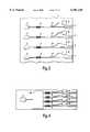
- FIG. 3is a schematic view of an array of external cavity laser such as that shown in FIG. 1 fined on a single chip;
- FIG. 4is a schematic view of an alternative arrangement providing an array of external cavity lasers on a single chip.
- FIG. 5is a schematic view of another arrangement providing an array of external cavity lasers on a single chip.
- FIG. 1shows an external cavity laser formed on an SOI chip 1 which comprises an upper, light transmissive layer of silicon separated from a silicon substrate by an insulating layer, typically of silicon dioxide.
- the devicecomprises an RA 2, aligned with a silicon waveguide 3 in which a grating 4 is provided.
- the RApreferably includes a waveguide therein at an angle to the normal of its front facet 2A.
- a back facet 2B of the RAis coated with a HR coating and the front facet thereof is AR coated.
- the RA 2is passively aligned on the SOI chip 1 by means of location surfaces of the RA being abutted against location surfaces of a location recess 5 etched in the SOI chip 1. Further details of this method of mounting an optical component are given in U.S. application Ser. No. 08/853,104; the disclosure of which is incorporated herein by reference.
- the RA 2is coupled to the silicon waveguide 3 within which a Bragg grating 4 is formed.
- the grating 4effectively forms the front facet of the external cavity laser.
- An NTC (negative temperature coefficient) thermistor 6is located next to the grating 4 to sense the temperature of the grating 4.
- the thermistor 6provides an input for a temperature compensation system comprising the thermistor 6, a control circuit (not shown), and a cooling device.
- the cooling devicemay comprise a Peltier cooler mounted underneath the chip so as to cool the chip or at least the grating 4 which determines the output wavelength. This temperature compensation system is provided to extend the operating range of the laser (as in an FGL) rather than for tuning the device to compensate for variations in the manufacturing process.
- An output fibre 7is located within an anisotropically etched V-groove in the SOI chip 1 to passively align the fibre to the silicon waveguide 3.
- a method of coupling a fibre to a rib waveguide on an SOI chipis described in U.S. application Ser. No. 08/643,476 the disclosure of which is incorporated herein by reference.
- the output of the external cavity lasermay also be directed to other optical devices provided on the same chip.
- a monitor photodiode 8is provided to monitor the output of the external cavity laser by means of a waveguide coupler 9 which couples a portion of the laser output into the photodiode 8.
- the coupler 9may comprise a Y-junction or an evanescent coupler.
- FIG. 2shows the grating 4 formed in the silicon waveguide 3 in more detail.
- the Bragg waveguide gratingforms a wavelength selective element and can be produced, for example, by direct electron beam writing onto a photoresist coating formed over the waveguide, the pattern then being etched using RIE (reactive ion etching) to form the grooves of the waveguide grating.
- RIEreactive ion etching
- the grooves of the gratingpreferably extend approximately halfway through the height H of the rib waveguide (whereby H is typically in the range 1.4-5 microns measured from the upper surface of the adjacent areas of the chip).
- the depth D of the groovesis chosen to optimise the grating coupling, i.e. its reflectivity, the output power of the laser and the optical losses associated with the grating, and preferably D is 30-70% of H.
- DIn a rib waveguide with H being 1.4-1.5 microns, D would thus be in the range 0.4 to 1.1 microns.
- the other dimensions of the gratingare determined by the wavelength to be selected but a typical grating would have a series of grooves with a 200 nm period P and a 50% mark/space ratio, i.e. each groove is approximately 100 nm wide (in the direction parallel to the optical axis of the waveguide) and spaced 100 nm from the adjacent grooves.
- the gratingwould typically extend over a length L of the waveguide of about 1 to 5 mm.
- the grooves of the grating 4may be filled or partially filled with other material, e.g. silicon dioxide, but the essential requirements of the grating are that it provide periodically alternating regions of different refractive index, so that it reflects a proportion of the selected wavelength, and that it can be formed using mass production techniques.
- other materiale.g. silicon dioxide
- the grating 4may be formed by grooves in a silicon dioxide cladding layer provided over the waveguide rib in place of, or in addition to, grooves in the silicon rib.
- the optical length of the laser cavityfrom the back facet 2B of the RA 2 to the effective reflective centre of the grating 4, would typically be of the order of 12 mm.
- siliconhas a refractive index of 3.5
- the physical length of the cavityis thus 12 mm/3.5, i.e. about 3.4 mm.
- the fibre to waveguide alignmentcan also be performed by butt coupling or any other suitable method of achieving good alignment between the waveguide and the fibre core.
- the use of front facet monitoring as described above and a 100% HR coating on the back facet 2B of the RA 2also enables higher output powers to be achieved.
- conventional back facet monitoringmay be used in place of the front facet monitoring described above.
- Manufacturability of the devicemay be improved by the use of phase interference masks to produce the waveguide grating. This would enable the grating lithography to be carried out on conventional contact lithography systems with a consequent reduction in production costs, and the possibility for very high volume production.
- the NTC thermistor 6is hybridised on the chip adjacent to the grating 4.
- Other types of hybridised sensormay be used, or a doped structure integrated into the SOI chip may be used.
- Possible structuresinclude a p-i-n diode or p-n junction, whose properties vary with temperature, provided adjacent or across the waveguide in which the grating is formed. The use of such a monolithic sensor reduces the number of assembly operations required and provides for optimum and repeatable positioning of the temperature sensor.
- the waveguide grating 4may also be provided on a thermally isolated substrate, such as that described in U.S. application Ser. No. 09/057,641 with the grating temperature maintained at a steady temperature by use of a resistive heater and a temperature sensor. This would remove the need for device cooling using a cooling device since it is the temperature of the grating 4 that determines the output wavelength of the laser.
- the gratingis formed on a portion of the silicon waveguide which is substantially thermally isolated from its surroundings.
- the portion of the waveguide in which the grating is formedmay, for example, be formed on a portion of a silicon layer which extends over a recess in the silicon chip, e.g. in the form of a bridge, or between trenches formed in adjacent areas of the silicon layer.
- the trenchespreferably extend through the silicon layer (which has a relatively high thermal conductivity) down to the insulating layer but may extend through the insulating layer further into the chip.
- the trenchesmay be V-grooves formed on either side of the rib waveguide.
- thermoelectric coolingrequires less power than thermoelectric cooling
- the use of a thermally isolated gratingalso make it feasible to integrate of the temperature control circuit into the laser module with consequent system benefits such as reduction in complexity of the drive circuit controlling the device.
- the arrangement described abovecould be used to fine-tune the wavelength of the laser, e.g. to adjust precisely to the. centre of a very narrow WDM band.
- SOI technologyfacilitates integration of devices so making it possible to provide an array of lasers on a single chip as shown in FIG. 3.
- Each of the lasers shown in FIG. 3is essentially identical to that described above in relation to FIGS. 1 and 2 but with each grating designed to reflect a different wavelength.
- SOI technologyenables each of the lasers in the array to be formed simultaneously using conventional lithographic techniques.
- the fibres 7 connected to the array of lasersmay be separate optical fibres or part of a fibre ribbon.
- a multiplexer device 12may be integrated with the laser array to multiplex the signals from each laser onto a single output waveguide 14 and so produce a single fibre multichannel WDM source.
- An external cavity laser or array of such lasers as described abovemay also be used as part of a transceiver by providing one or more photodiodes on the chip.
- FIG. 4shows an alternative form of array which comprises a single RA 2 connected to a plurality of gratings 4 to produce a multi-channel source with a reduced number of active elements.
- a dispersive power splitting element 10such as a transmission or reflection grating, or an array of cascaded Y-junctions, is incorporated between the RA 2 and the gratings 4.
- Such a devicewill have single mode outputs at each of the Bragg wavelengths of the respective gratings 4.
- the gratingmust be written into a silicon waveguide, preferably on an SOI chip.
- the deviceis very similar to a fibre grating laser (or other external cavity laser using a Bragg grating as a feedback element), the significant difference being that the use of integrated silicon optics enables mass production techniques to be employed, as well as the integration of further functions onto a single device with better manageability of the temperature characteristics of the device.
- the output wavelength of the laseris determined by the grating formed in the silicon waveguide so the output wavelength, at a given temperature, can be determined during manufacture of the device, without the need to tune the device, and all parts of the laser can be made by mass production techniques.
- SOI technologyleads to significantly reduced production costs compared to the prior art and enables volume production of devices.
- SOI technologyalso enables passive alignment of active elements on the device with repeatable and accurate positioning. Further SOI technology allows for additional functionality within a single module, for example the addition of MUX/DMUX and Rx (receiver) elements.
- the use of SOI waveguidesalso enables the use of front facet monitoring of the laser using a waveguide coupler to couple a proportion of the output light into a monitor photodiode. This reduces tracking error (the difference between the actual power in the fibre compared to that inferred from the monitor photodiode) and removes the need for back facet monitoring (which is required to provide power monitoring for all devices described by the prior art). This makes possible a more efficient laser since the HR coating on the back facet can be increased to 100% reflection.
Landscapes
- Physics & Mathematics (AREA)
- Condensed Matter Physics & Semiconductors (AREA)
- General Physics & Mathematics (AREA)
- Electromagnetism (AREA)
- Optics & Photonics (AREA)
- Optical Integrated Circuits (AREA)
- Semiconductor Lasers (AREA)
- Optical Couplings Of Light Guides (AREA)
Abstract
Description
Claims (16)
Applications Claiming Priority (2)
| Application Number | Priority Date | Filing Date | Title |
|---|---|---|---|
| GB9815070AGB2325334B (en) | 1998-07-10 | 1998-07-10 | External cavity laser |
| GB9815070 | 1998-07-10 |
Publications (1)
| Publication Number | Publication Date |
|---|---|
| US6101210Atrue US6101210A (en) | 2000-08-08 |
Family
ID=10835357
Family Applications (1)
| Application Number | Title | Priority Date | Filing Date |
|---|---|---|---|
| US09/144,075Expired - LifetimeUS6101210A (en) | 1998-07-10 | 1998-08-31 | External cavity laser |
Country Status (11)
| Country | Link |
|---|---|
| US (1) | US6101210A (en) |
| EP (1) | EP1097394B1 (en) |
| JP (1) | JP2002520858A (en) |
| KR (1) | KR20010071852A (en) |
| CN (1) | CN1309827A (en) |
| AU (1) | AU1344299A (en) |
| CA (1) | CA2336981A1 (en) |
| DE (1) | DE69808342T2 (en) |
| GB (1) | GB2325334B (en) |
| IL (1) | IL140587A0 (en) |
| WO (1) | WO2000003461A1 (en) |
Cited By (80)
| Publication number | Priority date | Publication date | Assignee | Title |
|---|---|---|---|---|
| US6278721B1 (en)* | 1999-03-03 | 2001-08-21 | Lucent Technologies, Inc. | Method for minimizing locking range variability of a laser module |
| US6316281B1 (en)* | 1998-09-12 | 2001-11-13 | Electronics And Telecommunications Research Institute | Method for fabricating a hybrid optical integrated circuit employing SOI optical waveguide |
| US20020037025A1 (en)* | 2000-09-25 | 2002-03-28 | Bartman Randall K. | Hybrid narrow -linewidth semiconductor lasers |
| US20020106150A1 (en)* | 2000-11-27 | 2002-08-08 | Bendett Mark P. | Apparatus and method for integrated photonic devices having high-performance waveguides and multicompositional substrates |
| GB2378811A (en)* | 2001-08-16 | 2003-02-19 | Bookham Technology Plc | A Laser System |
| US6525864B1 (en) | 2000-07-20 | 2003-02-25 | Nayna Networks, Inc. | Integrated mirror array and circuit device |
| US20030047738A1 (en)* | 2001-08-28 | 2003-03-13 | The Furukawa Electric Co., Ltd. | Semiconductor laser device having selective absorption qualities over a wide temperature range |
| US20030053495A1 (en)* | 2001-09-10 | 2003-03-20 | Woodley Bruce Robert | Wavelength agile laser |
| US20030095737A1 (en)* | 2001-10-09 | 2003-05-22 | Welch David F. | Transmitter photonic integrated circuits (TxPIC) and optical transport networks employing TxPICs |
| WO2002054544A3 (en)* | 2001-01-02 | 2003-09-04 | Fiberspace Inc | Tunable semiconductor laser having a cavity with wavelength selective mirror and mach-tehnder interferometer |
| US20030185514A1 (en)* | 2002-03-29 | 2003-10-02 | Bendett Mark P. | Method and apparatus for tapping a waveguide on a substrate |
| US6661945B2 (en) | 2000-04-28 | 2003-12-09 | Kaiser Optical Systems, Inc. | Multi-band wavelength dispersive device for use in dense wavelength division multiplexing (DWDM) networks |
| US20030231686A1 (en)* | 2002-06-13 | 2003-12-18 | Ansheng Liu | Method and apparatus for tunable wavelength conversion using a bragg grating and a laser in a semiconductor substrate |
| US20040020896A1 (en)* | 2002-02-15 | 2004-02-05 | Lockheed Martin Corporation | Tapered optical fiber for fiber to waveguide interconnection |
| WO2002065600A3 (en)* | 2001-02-14 | 2004-02-26 | Gemfire Corp | Multi-channel laser pump source and packaging method therefor |
| WO2004034530A1 (en)* | 2002-10-08 | 2004-04-22 | Infinera Corporation | TRANSMITTER PHOTONIC INTEGRATED CIRCUIT (TxPIC) CHIPS |
| US6771851B1 (en) | 2001-06-19 | 2004-08-03 | Nayna Networks | Fast switching method for a micro-mirror device for optical switching applications |
| US20040264856A1 (en)* | 2003-06-30 | 2004-12-30 | Mina Farr | Micro-module with micro-lens |
| US20050025420A1 (en)* | 2003-06-30 | 2005-02-03 | Mina Farr | Optical sub-assembly laser mount having integrated microlens |
| US20050046928A1 (en)* | 2001-02-14 | 2005-03-03 | Gemfire Corporation | Multi-channel laser pump source for optical amplifiers |
| US6888863B1 (en) | 2000-06-30 | 2005-05-03 | Lucent Technologies Inc. | System comprising optical semiconductor waveguide device |
| US20050129402A1 (en)* | 2003-10-21 | 2005-06-16 | Kim Byoung W. | WDM-PON system with optical wavelength alignment function |
| US6941043B1 (en)* | 2001-07-10 | 2005-09-06 | K2 Optronics, Inc. | Wavelength stabilization of an external cavity laser diode (ECLD) |
| US6947457B2 (en)* | 2000-02-14 | 2005-09-20 | Yokogawa Electric Corporation | DFB laser driving device, DFB laser driving method and storage medium |
| US6970494B1 (en) | 1999-01-27 | 2005-11-29 | Teem Photonics, S.A. | Rare-earth doped phosphate-glass lasers and associated methods |
| US20060002443A1 (en)* | 2004-06-30 | 2006-01-05 | Gennady Farber | Multimode external cavity semiconductor lasers |
| US20060133730A1 (en)* | 2004-05-04 | 2006-06-22 | Electronics And Telecommunications Research Institute | Base station optical line terminal of passive optical subscriber network using wavelength division multiplexing method and method for manufacturing the same |
| US20060177177A1 (en)* | 2003-03-22 | 2006-08-10 | Qinetiq Limited | Optical wavelength division multiplexer/demultiplexer device |
| US7092419B2 (en) | 2001-09-10 | 2006-08-15 | San Jose Systems, Inc. | Wavelength agile laser |
| US20070041679A1 (en)* | 2005-07-01 | 2007-02-22 | Zhaoran Huang | Integrated thin film MSM photodetector/grating for WDM |
| US20070077005A1 (en)* | 2005-10-05 | 2007-04-05 | Doosan Corporation | Optical waveguide having curved reflecting mirror surface and method of manufacturing the same |
| US20070280326A1 (en)* | 2005-12-16 | 2007-12-06 | Sioptical, Inc. | External cavity laser in thin SOI with monolithic electronics |
| US20080031626A1 (en)* | 2001-10-09 | 2008-02-07 | Infinera Corporation | Photonic Integrated Circuit (PIC) Chips |
| US20080044128A1 (en)* | 2001-10-09 | 2008-02-21 | Infinera Corporation | TRANSMITTER PHOTONIC INTEGRATED CIRCUITS (TxPICs) AND OPTICAL TRANSPORT NETWORK SYSTEM EMPLOYING TxPICs |
| US20080088928A1 (en)* | 2006-10-13 | 2008-04-17 | Kaiser Optical Systems | Optical configurations for achieving uniform channel spacing in wdm telecommunications applications |
| US20080138088A1 (en)* | 2001-10-09 | 2008-06-12 | Infinera Corporation | Monolithic transmitter photonic integrated circuit (txpic) having tunable modulated sources with feedback system for source power level or wavelength tuning |
| US20080181561A1 (en)* | 2006-12-26 | 2008-07-31 | Hideto Furuyama | Optoelectronic interconnection board, optoelectronic interconnection apparatus, and manufacturing method thereof |
| US20090021835A1 (en)* | 2002-10-08 | 2009-01-22 | Infinera Corporation | TILTED COMBINERS/DECOMBINERS AND PHOTONIC INTEGRATED CIRCUITS (PICs) EMPLOYING THE SAME |
| US7565084B1 (en) | 2004-09-15 | 2009-07-21 | Wach Michael L | Robustly stabilizing laser systems |
| US20090225797A1 (en)* | 2004-07-30 | 2009-09-10 | Osram Opto Semiconductors Gmbh | Semiconductor laser component , optical device for a semiconductor laser component, and method for producing an optical device |
| US20110085577A1 (en)* | 2009-10-13 | 2011-04-14 | Skorpios Technologies, Inc. | Method and system of heterogeneous substrate bonding for photonic integration |
| US20110085572A1 (en)* | 2009-10-13 | 2011-04-14 | Skorpios Technologies, Inc. | Method and system for hybrid integration of a tunable laser |
| US20120057079A1 (en)* | 2009-10-13 | 2012-03-08 | Skorpios Technolgies, Inc. | Method and system for hybrid integration of a tunable laser for a cable tv transmitter |
| US20120057609A1 (en)* | 2009-10-13 | 2012-03-08 | Skorpios Technologies, Inc. | Method and system for hybrid integration of a tunable laser and a mach zehnder modulator |
| US20120057610A1 (en)* | 2009-10-13 | 2012-03-08 | Skorpios Technologies, Inc. | Method and system for hybrid integration of a tunable laser and a phase modulator |
| US20120082016A1 (en)* | 2010-10-05 | 2012-04-05 | Tdk Corporation | Optical waveguide and thermally-assisted magnetic recording head therewith |
| US20120099611A1 (en)* | 2009-06-12 | 2012-04-26 | Mel | External cavity tunable laser module |
| US8368995B2 (en) | 2009-10-13 | 2013-02-05 | Skorpios Technologies, Inc. | Method and system for hybrid integration of an opto-electronic integrated circuit |
| WO2013055396A1 (en)* | 2011-10-14 | 2013-04-18 | Kotura, Inc. | Reduction of mode hopping in a laser cavity |
| US8611388B2 (en) | 2009-10-13 | 2013-12-17 | Skorpios Technologies, Inc. | Method and system for heterogeneous substrate bonding of waveguide receivers |
| US20140199020A1 (en)* | 2011-03-31 | 2014-07-17 | Thales | System for transmitting optical signals |
| US20150207291A1 (en)* | 2014-01-20 | 2015-07-23 | Rockley Photonics Limited | Tunable soi laser |
| US9240673B2 (en) | 2014-01-20 | 2016-01-19 | Rockley Photonics Limited | Tunable SOI laser |
| CN105428998A (en)* | 2015-12-28 | 2016-03-23 | 中国科学院半导体研究所 | External cavity narrow linewidth laser device |
| US9316785B2 (en) | 2013-10-09 | 2016-04-19 | Skorpios Technologies, Inc. | Integration of an unprocessed, direct-bandgap chip into a silicon photonic device |
| WO2016073506A1 (en)* | 2014-11-05 | 2016-05-12 | Coriant Advanced Technology, LLC | Photonic integrated circuit incorporating a bandgap temperature sensor |
| US9356419B1 (en) | 2015-04-09 | 2016-05-31 | International Business Machines Corporation | Temperature insensitive external cavity lasers on silicon |
| US9379515B1 (en) | 2011-02-10 | 2016-06-28 | Mellanox Technologies Silicon Photonics Inc. | Laser combining light signals from multiple laser cavities |
| US9496431B2 (en) | 2013-10-09 | 2016-11-15 | Skorpios Technologies, Inc. | Coplanar integration of a direct-bandgap chip into a silicon photonic device |
| US9513437B2 (en) | 2014-11-05 | 2016-12-06 | Coriant Advanced Technology, LLC | Photonic integrated circuit incorporating a bandgap temperature sensor |
| TWI569548B (en)* | 2009-10-13 | 2017-02-01 | 思科皮爾斯科技公司 | Method and system for hybrid integration of a tunable laser |
| US9829630B2 (en) | 2011-09-08 | 2017-11-28 | Skorpios Technologies, Inc. | Tunable reflectors based on multi-cavity interference |
| US9829631B2 (en) | 2015-04-20 | 2017-11-28 | Skorpios Technologies, Inc. | Vertical output couplers for photonic devices |
| US9885832B2 (en) | 2014-05-27 | 2018-02-06 | Skorpios Technologies, Inc. | Waveguide mode expander using amorphous silicon |
| WO2018060710A1 (en)* | 2016-09-30 | 2018-04-05 | Oclaro Technology Limited | Tuneable dbr laser without external frequency locker |
| US9977188B2 (en) | 2011-08-30 | 2018-05-22 | Skorpios Technologies, Inc. | Integrated photonics mode expander |
| US10003173B2 (en) | 2014-04-23 | 2018-06-19 | Skorpios Technologies, Inc. | Widely tunable laser control |
| US10088629B2 (en) | 2014-03-07 | 2018-10-02 | Skorpios Technologies, Inc. | Wide shoulder, high order mode filter for thick-silicon waveguides |
| US10649148B2 (en) | 2017-10-25 | 2020-05-12 | Skorpios Technologies, Inc. | Multistage spot size converter in silicon photonics |
| CN111323879A (en)* | 2020-04-13 | 2020-06-23 | 易锐光电科技(安徽)有限公司 | Optical module |
| US10811848B2 (en) | 2017-06-14 | 2020-10-20 | Rockley Photonics Limited | Broadband arbitrary wavelength multichannel laser source |
| US11177627B2 (en) | 2016-02-19 | 2021-11-16 | Rockley Photonics Limited | Tunable laser |
| US11181688B2 (en) | 2009-10-13 | 2021-11-23 | Skorpios Technologies, Inc. | Integration of an unprocessed, direct-bandgap chip into a silicon photonic device |
| US11183492B2 (en) | 2010-12-08 | 2021-11-23 | Skorpios Technologies, Inc. | Multilevel template assisted wafer bonding |
| US11360263B2 (en) | 2019-01-31 | 2022-06-14 | Skorpios Technologies. Inc. | Self-aligned spot size converter |
| US20230072926A1 (en)* | 2021-09-03 | 2023-03-09 | Freedom Photonics Llc | Multiwavelength optical sources |
| US20230187903A1 (en)* | 2020-05-25 | 2023-06-15 | Nippon Telegraph And Telephone Corporation | Tunable Laser Diode |
| US11699892B2 (en) | 2016-02-19 | 2023-07-11 | Rockley Photonics Limited | Discrete wavelength tunable laser |
| US12368283B2 (en) | 2017-06-14 | 2025-07-22 | Rockley Photonics Limited | Broadband arbitrary wavelength multichannel laser source |
| US12444723B2 (en) | 2022-09-20 | 2025-10-14 | Skorpios Technologies, Inc. | Heterogeneous bonding for photonic integration |
Families Citing this family (7)
| Publication number | Priority date | Publication date | Assignee | Title |
|---|---|---|---|---|
| GB2353898A (en)* | 1999-08-25 | 2001-03-07 | Bookham Technology Ltd | A semiconductor laser amplifier using waveguides |
| SE524828C2 (en)* | 2002-06-06 | 2004-10-12 | Alfa Exx Ab | Resonator |
| DE10240949A1 (en)* | 2002-09-02 | 2004-03-04 | Hentze-Lissotschenko Patentverwaltungs Gmbh & Co.Kg | Semiconducting laser device has at least one external reflection arrangement with concave reflective surface that can reflect at least some laser light back to influence laser light mode spectrum |
| US7228030B2 (en)* | 2004-03-29 | 2007-06-05 | Intel Corporation | Method and apparatus providing an output coupler for an optical beam |
| KR100647904B1 (en) | 2004-12-20 | 2006-11-23 | 한국전자통신연구원 | Method for manufacturing laser having optical Bragg grating external resonator and laser produced by |
| FR2909491B1 (en)* | 2006-12-05 | 2010-04-23 | Commissariat Energie Atomique | LASER SOURCE LASER DEVICE AND TORQUE WAVEGUIDE |
| CN102565955B (en)* | 2012-01-16 | 2013-03-20 | 中国科学院半导体研究所 | Electric tunable grating coupler |
Citations (1)
| Publication number | Priority date | Publication date | Assignee | Title |
|---|---|---|---|---|
| US4911512A (en)* | 1986-11-05 | 1990-03-27 | Sharp Kabushiki Kaisha | Waveguide type optical head |
Family Cites Families (4)
| Publication number | Priority date | Publication date | Assignee | Title |
|---|---|---|---|---|
| US5537432A (en)* | 1993-01-07 | 1996-07-16 | Sdl, Inc. | Wavelength-stabilized, high power semiconductor laser |
| US6064783A (en)* | 1994-05-25 | 2000-05-16 | Congdon; Philip A. | Integrated laser and coupled waveguide |
| JPH10148726A (en)* | 1996-11-19 | 1998-06-02 | Mitsubishi Electric Corp | Optical waveguide grating, method of manufacturing the same, optical filter using the optical waveguide grating, and wavelength division multiplexing optical transmission system using the optical filter |
| GB2320104B (en)* | 1997-10-16 | 1998-11-18 | Bookham Technology Ltd | Thermally isolated silicon layer |
- 1998
- 1998-07-10GBGB9815070Apatent/GB2325334B/ennot_activeExpired - Fee Related
- 1998-08-31USUS09/144,075patent/US6101210A/ennot_activeExpired - Lifetime
- 1998-12-02WOPCT/GB1998/003595patent/WO2000003461A1/ennot_activeApplication Discontinuation
- 1998-12-02JPJP2000559620Apatent/JP2002520858A/ennot_activeWithdrawn
- 1998-12-02ILIL14058798Apatent/IL140587A0/enunknown
- 1998-12-02AUAU13442/99Apatent/AU1344299A/ennot_activeAbandoned
- 1998-12-02DEDE69808342Tpatent/DE69808342T2/ennot_activeExpired - Fee Related
- 1998-12-02EPEP98957012Apatent/EP1097394B1/ennot_activeExpired - Lifetime
- 1998-12-02CNCN98814221Apatent/CN1309827A/enactivePending
- 1998-12-02CACA002336981Apatent/CA2336981A1/ennot_activeAbandoned
- 1998-12-02KRKR1020017000455Apatent/KR20010071852A/ennot_activeWithdrawn
Patent Citations (1)
| Publication number | Priority date | Publication date | Assignee | Title |
|---|---|---|---|---|
| US4911512A (en)* | 1986-11-05 | 1990-03-27 | Sharp Kabushiki Kaisha | Waveguide type optical head |
Cited By (148)
| Publication number | Priority date | Publication date | Assignee | Title |
|---|---|---|---|---|
| US6316281B1 (en)* | 1998-09-12 | 2001-11-13 | Electronics And Telecommunications Research Institute | Method for fabricating a hybrid optical integrated circuit employing SOI optical waveguide |
| US6970494B1 (en) | 1999-01-27 | 2005-11-29 | Teem Photonics, S.A. | Rare-earth doped phosphate-glass lasers and associated methods |
| US6278721B1 (en)* | 1999-03-03 | 2001-08-21 | Lucent Technologies, Inc. | Method for minimizing locking range variability of a laser module |
| US6947457B2 (en)* | 2000-02-14 | 2005-09-20 | Yokogawa Electric Corporation | DFB laser driving device, DFB laser driving method and storage medium |
| US6661945B2 (en) | 2000-04-28 | 2003-12-09 | Kaiser Optical Systems, Inc. | Multi-band wavelength dispersive device for use in dense wavelength division multiplexing (DWDM) networks |
| US6888863B1 (en) | 2000-06-30 | 2005-05-03 | Lucent Technologies Inc. | System comprising optical semiconductor waveguide device |
| US6525864B1 (en) | 2000-07-20 | 2003-02-25 | Nayna Networks, Inc. | Integrated mirror array and circuit device |
| US20020037025A1 (en)* | 2000-09-25 | 2002-03-28 | Bartman Randall K. | Hybrid narrow -linewidth semiconductor lasers |
| US6954564B2 (en) | 2000-11-27 | 2005-10-11 | Teem Photonics | Apparatus and method for integrated photonic devices having high-performance waveguides and multicompositional substrates |
| US20020106150A1 (en)* | 2000-11-27 | 2002-08-08 | Bendett Mark P. | Apparatus and method for integrated photonic devices having high-performance waveguides and multicompositional substrates |
| WO2002054544A3 (en)* | 2001-01-02 | 2003-09-04 | Fiberspace Inc | Tunable semiconductor laser having a cavity with wavelength selective mirror and mach-tehnder interferometer |
| WO2002065600A3 (en)* | 2001-02-14 | 2004-02-26 | Gemfire Corp | Multi-channel laser pump source and packaging method therefor |
| US20050046928A1 (en)* | 2001-02-14 | 2005-03-03 | Gemfire Corporation | Multi-channel laser pump source for optical amplifiers |
| US7653109B2 (en) | 2001-02-14 | 2010-01-26 | Gemfire Corporation | Multi-channel laser pump source for optical amplifiers |
| US7235150B2 (en) | 2001-02-14 | 2007-06-26 | Gemfire Corporation | Multi-channel laser pump source for optical amplifiers |
| US20070248139A1 (en)* | 2001-02-14 | 2007-10-25 | Gemfire Corporation | Multi-Channel Laser Pump Source for Optical Amplifiers |
| US6771851B1 (en) | 2001-06-19 | 2004-08-03 | Nayna Networks | Fast switching method for a micro-mirror device for optical switching applications |
| US6941043B1 (en)* | 2001-07-10 | 2005-09-06 | K2 Optronics, Inc. | Wavelength stabilization of an external cavity laser diode (ECLD) |
| US20030035449A1 (en)* | 2001-08-16 | 2003-02-20 | Andrew Tomlinson | Laser systems |
| GB2378811A (en)* | 2001-08-16 | 2003-02-19 | Bookham Technology Plc | A Laser System |
| US20030047738A1 (en)* | 2001-08-28 | 2003-03-13 | The Furukawa Electric Co., Ltd. | Semiconductor laser device having selective absorption qualities over a wide temperature range |
| US7092419B2 (en) | 2001-09-10 | 2006-08-15 | San Jose Systems, Inc. | Wavelength agile laser |
| US6987784B2 (en) | 2001-09-10 | 2006-01-17 | San Jose Systems, Inc. | Wavelength agile laser |
| US20030053495A1 (en)* | 2001-09-10 | 2003-03-20 | Woodley Bruce Robert | Wavelength agile laser |
| US7062114B2 (en) | 2001-10-09 | 2006-06-13 | Infinera Corporation | Submount for a photonic integrated circuit (PIC) chip |
| US20070242918A1 (en)* | 2001-10-09 | 2007-10-18 | Infinera Corporation | Transmitter Photonic Integrated Circuits (TxPICs) with Directly Modulated Lasers and Wavelength Selective Combiners |
| US20050063636A1 (en)* | 2001-10-09 | 2005-03-24 | Infinera Corporation | Method and apparatus for providing an antireflection coating on the output facet of a photonic integrated circuit (PIC) chip |
| US20050025409A1 (en)* | 2001-10-09 | 2005-02-03 | Infinera Corporation | Submount for a photonic integrated circuit (PIC) chip |
| US20050094926A1 (en)* | 2001-10-09 | 2005-05-05 | Infinera Corporation | Method of calibrating a monolithic transmitter photonic integrated circuit (TxPIC) chip |
| US20050094925A1 (en)* | 2001-10-09 | 2005-05-05 | Infinera Corporation | Method of in-wafer testing of monolithic photonic integrated circuits (PICs) formed in a semiconductor wafer |
| US20050094927A1 (en)* | 2001-10-09 | 2005-05-05 | Infinera Corporation | Probe card for testing in-wafer photonic integrated circuits (PICs) and method of use |
| US20050100345A1 (en)* | 2001-10-09 | 2005-05-12 | Infinera Corporation | Monolithic transmitter/receiver photonic integrated circuit (Tx/RxPIC) transceiver chip |
| US7792396B2 (en) | 2001-10-09 | 2010-09-07 | Infinera Corporation | Probe card for testing in-wafer photonic integrated circuits (PICs) and method of use |
| US7460742B2 (en) | 2001-10-09 | 2008-12-02 | Infinera Corporation | Method and apparatus for providing an antireflection coating on the output facet of a photonic integrated circuit (PIC) chip |
| US7885492B2 (en) | 2001-10-09 | 2011-02-08 | Infinera Corporation | Transmitter photonic integrated circuit (TxPIC) chips |
| US20080044128A1 (en)* | 2001-10-09 | 2008-02-21 | Infinera Corporation | TRANSMITTER PHOTONIC INTEGRATED CIRCUITS (TxPICs) AND OPTICAL TRANSPORT NETWORK SYSTEM EMPLOYING TxPICs |
| US20040067006A1 (en)* | 2001-10-09 | 2004-04-08 | Welch David F. | Transmitter photonic integrated circuit ( TxPIC) chips |
| US7680368B2 (en) | 2001-10-09 | 2010-03-16 | Infinera Corporation | Monolithic transmitter photonic integrated circuit (TxPIC) with a traversely disposed output |
| WO2003032021A3 (en)* | 2001-10-09 | 2004-03-25 | Infinera Corp | TRANSMITTER PHOTONIC INTEGRATED CIRCUITS (TxPIC) AND OPTICAL TRANSPORT NETWORKS EMPLOYING TxPICs |
| US20060023992A1 (en)* | 2001-10-09 | 2006-02-02 | Infinera Corporation | Method of in-wafer testing of monolithic photonic integrated circuits (PICs) formed in a semiconductor wafer |
| US7043109B2 (en) | 2001-10-09 | 2006-05-09 | Infinera Corporation | Method of in-wafer testing of monolithic photonic integrated circuits (PICs) formed in a semiconductor wafer |
| US20080138088A1 (en)* | 2001-10-09 | 2008-06-12 | Infinera Corporation | Monolithic transmitter photonic integrated circuit (txpic) having tunable modulated sources with feedback system for source power level or wavelength tuning |
| US7672546B2 (en) | 2001-10-09 | 2010-03-02 | Infinera Corporation | Optical transport network having a plurality of monolithic photonic integrated circuit semiconductor chips |
| US20080031626A1 (en)* | 2001-10-09 | 2008-02-07 | Infinera Corporation | Photonic Integrated Circuit (PIC) Chips |
| US7466882B2 (en) | 2001-10-09 | 2008-12-16 | Infinera Corporation | Monolithic transmitter/receiver photonic integrated circuit (Tx/RxPIC) transceiver chip |
| US7519246B2 (en) | 2001-10-09 | 2009-04-14 | Infinera Corporation | Photonic integrated circuit (PIC) chips |
| US7483599B2 (en) | 2001-10-09 | 2009-01-27 | Infinera Corporation | Method of calibrating a monolithic transmitter photonic integrated circuit (TXPIC) chip |
| US7477807B2 (en) | 2001-10-09 | 2009-01-13 | Infinera Corporation | Monolithic transmitter photonic integrated circuit (TxPIC) semiconductor chip |
| US7283694B2 (en) | 2001-10-09 | 2007-10-16 | Infinera Corporation | Transmitter photonic integrated circuits (TxPIC) and optical transport networks employing TxPICs |
| US7751658B2 (en) | 2001-10-09 | 2010-07-06 | Infinera Corporation | Monolithic transmitter photonic integrated circuit (TxPIC) having tunable modulated sources with feedback system for source power level or wavelength tuning |
| US20070248299A1 (en)* | 2001-10-09 | 2007-10-25 | Infinera Corporation | Monolithic Transmitter Photonic Integrated Circuit (TxPIC) Semiconductor Chip |
| US20030095737A1 (en)* | 2001-10-09 | 2003-05-22 | Welch David F. | Transmitter photonic integrated circuits (TxPIC) and optical transport networks employing TxPICs |
| US20040020896A1 (en)* | 2002-02-15 | 2004-02-05 | Lockheed Martin Corporation | Tapered optical fiber for fiber to waveguide interconnection |
| US20030185514A1 (en)* | 2002-03-29 | 2003-10-02 | Bendett Mark P. | Method and apparatus for tapping a waveguide on a substrate |
| WO2003083538A3 (en)* | 2002-03-29 | 2004-04-08 | Teem Photonics | Method and apparatus for tapping optical waveguides |
| US20030231686A1 (en)* | 2002-06-13 | 2003-12-18 | Ansheng Liu | Method and apparatus for tunable wavelength conversion using a bragg grating and a laser in a semiconductor substrate |
| US6788727B2 (en)* | 2002-06-13 | 2004-09-07 | Intel Corporation | Method and apparatus for tunable wavelength conversion using a bragg grating and a laser in a semiconductor substrate |
| US7747114B2 (en) | 2002-10-08 | 2010-06-29 | Infinera Corporation | Tilted combiners/decombiners and photonic integrated circuits (PICs) employing the same |
| US20090021835A1 (en)* | 2002-10-08 | 2009-01-22 | Infinera Corporation | TILTED COMBINERS/DECOMBINERS AND PHOTONIC INTEGRATED CIRCUITS (PICs) EMPLOYING THE SAME |
| WO2004034530A1 (en)* | 2002-10-08 | 2004-04-22 | Infinera Corporation | TRANSMITTER PHOTONIC INTEGRATED CIRCUIT (TxPIC) CHIPS |
| US20060177177A1 (en)* | 2003-03-22 | 2006-08-10 | Qinetiq Limited | Optical wavelength division multiplexer/demultiplexer device |
| US7689075B2 (en)* | 2003-03-22 | 2010-03-30 | Qinetiq Limited | Optical wavelength division multiplexer/demultiplexer device |
| US20040264856A1 (en)* | 2003-06-30 | 2004-12-30 | Mina Farr | Micro-module with micro-lens |
| US7422377B2 (en)* | 2003-06-30 | 2008-09-09 | Finisar Corporation | Micro-module with micro-lens |
| US20050025420A1 (en)* | 2003-06-30 | 2005-02-03 | Mina Farr | Optical sub-assembly laser mount having integrated microlens |
| US7327771B2 (en)* | 2003-10-21 | 2008-02-05 | Electronics And Telecommunications Research Institute | WDM-PON system with optical wavelength alignment function |
| US20050129402A1 (en)* | 2003-10-21 | 2005-06-16 | Kim Byoung W. | WDM-PON system with optical wavelength alignment function |
| US20060133730A1 (en)* | 2004-05-04 | 2006-06-22 | Electronics And Telecommunications Research Institute | Base station optical line terminal of passive optical subscriber network using wavelength division multiplexing method and method for manufacturing the same |
| US20060002443A1 (en)* | 2004-06-30 | 2006-01-05 | Gennady Farber | Multimode external cavity semiconductor lasers |
| US20090225797A1 (en)* | 2004-07-30 | 2009-09-10 | Osram Opto Semiconductors Gmbh | Semiconductor laser component , optical device for a semiconductor laser component, and method for producing an optical device |
| US7860144B2 (en) | 2004-07-30 | 2010-12-28 | Osram Opto Semiconductors Gmbh | Semiconductor laser component, optical device for a semiconductor laser component, and method for producing an optical device |
| US8521038B1 (en) | 2004-09-15 | 2013-08-27 | Cirrex Systems, Llc | Robustly stabilizing laser systems |
| US7565084B1 (en) | 2004-09-15 | 2009-07-21 | Wach Michael L | Robustly stabilizing laser systems |
| US7965949B1 (en) | 2004-09-15 | 2011-06-21 | Cirrex Systems Llc | Robustly stabilizing laser systems |
| US9065572B1 (en) | 2004-09-15 | 2015-06-23 | Cirrex Systems, Llc | Robustly stabilizing laser systems |
| US20070041679A1 (en)* | 2005-07-01 | 2007-02-22 | Zhaoran Huang | Integrated thin film MSM photodetector/grating for WDM |
| US20070077005A1 (en)* | 2005-10-05 | 2007-04-05 | Doosan Corporation | Optical waveguide having curved reflecting mirror surface and method of manufacturing the same |
| WO2007078836A3 (en)* | 2005-12-16 | 2008-04-24 | Sioptical Inc | External cavity laser in thin soi with monolithic electronics |
| US20070280326A1 (en)* | 2005-12-16 | 2007-12-06 | Sioptical, Inc. | External cavity laser in thin SOI with monolithic electronics |
| US20080088928A1 (en)* | 2006-10-13 | 2008-04-17 | Kaiser Optical Systems | Optical configurations for achieving uniform channel spacing in wdm telecommunications applications |
| US20080181561A1 (en)* | 2006-12-26 | 2008-07-31 | Hideto Furuyama | Optoelectronic interconnection board, optoelectronic interconnection apparatus, and manufacturing method thereof |
| US7623743B2 (en)* | 2006-12-26 | 2009-11-24 | Kabushiki Kaisha Toshiba | Optoelectronic interconnection board, optoelectronic interconnection apparatus, and manufacturing method thereof |
| US20120099611A1 (en)* | 2009-06-12 | 2012-04-26 | Mel | External cavity tunable laser module |
| US9190400B2 (en) | 2009-10-13 | 2015-11-17 | Skorpios Technologies, Inc. | Method and system for heterogeneous substrate bonding for photonic integration |
| US20110085572A1 (en)* | 2009-10-13 | 2011-04-14 | Skorpios Technologies, Inc. | Method and system for hybrid integration of a tunable laser |
| US9709735B2 (en) | 2009-10-13 | 2017-07-18 | Skorpios Technologies, Inc. | Method and system for heterogeneous substrate bonding for photonic integration |
| US20120057609A1 (en)* | 2009-10-13 | 2012-03-08 | Skorpios Technologies, Inc. | Method and system for hybrid integration of a tunable laser and a mach zehnder modulator |
| TWI569548B (en)* | 2009-10-13 | 2017-02-01 | 思科皮爾斯科技公司 | Method and system for hybrid integration of a tunable laser |
| US8368995B2 (en) | 2009-10-13 | 2013-02-05 | Skorpios Technologies, Inc. | Method and system for hybrid integration of an opto-electronic integrated circuit |
| US10373939B2 (en) | 2009-10-13 | 2019-08-06 | Skorpios Technologies, Inc. | Hybrid integrated optical device |
| US20120057079A1 (en)* | 2009-10-13 | 2012-03-08 | Skorpios Technolgies, Inc. | Method and system for hybrid integration of a tunable laser for a cable tv transmitter |
| US8559470B2 (en)* | 2009-10-13 | 2013-10-15 | Skorpios Technologies, Inc. | Method and system for hybrid integration of a tunable laser and a phase modulator |
| US8605766B2 (en)* | 2009-10-13 | 2013-12-10 | Skorpios Technologies, Inc. | Method and system for hybrid integration of a tunable laser and a mach zehnder modulator |
| US8611388B2 (en) | 2009-10-13 | 2013-12-17 | Skorpios Technologies, Inc. | Method and system for heterogeneous substrate bonding of waveguide receivers |
| US8615025B2 (en)* | 2009-10-13 | 2013-12-24 | Skorpios Technologies, Inc. | Method and system for hybrid integration of a tunable laser |
| US8630326B2 (en) | 2009-10-13 | 2014-01-14 | Skorpios Technologies, Inc. | Method and system of heterogeneous substrate bonding for photonic integration |
| US11181688B2 (en) | 2009-10-13 | 2021-11-23 | Skorpios Technologies, Inc. | Integration of an unprocessed, direct-bandgap chip into a silicon photonic device |
| US8867578B2 (en)* | 2009-10-13 | 2014-10-21 | Skorpios Technologies, Inc. | Method and system for hybrid integration of a tunable laser for a cable TV transmitter |
| US20110085577A1 (en)* | 2009-10-13 | 2011-04-14 | Skorpios Technologies, Inc. | Method and system of heterogeneous substrate bonding for photonic integration |
| US12287510B2 (en) | 2009-10-13 | 2025-04-29 | Skorpios Technologies, Inc. | Integration of an unprocessed, direct-bandgap chip into a silicon photonic device |
| US20120057610A1 (en)* | 2009-10-13 | 2012-03-08 | Skorpios Technologies, Inc. | Method and system for hybrid integration of a tunable laser and a phase modulator |
| US11482513B2 (en) | 2009-10-13 | 2022-10-25 | Skorpios Technologies, Inc. | Heterogeneous substrate bonding for photonic integration |
| US8270791B2 (en)* | 2010-10-05 | 2012-09-18 | Tdk Corporation | Optical waveguide and thermally-assisted magnetic recording head therewith |
| US20120082016A1 (en)* | 2010-10-05 | 2012-04-05 | Tdk Corporation | Optical waveguide and thermally-assisted magnetic recording head therewith |
| US11183492B2 (en) | 2010-12-08 | 2021-11-23 | Skorpios Technologies, Inc. | Multilevel template assisted wafer bonding |
| US9379515B1 (en) | 2011-02-10 | 2016-06-28 | Mellanox Technologies Silicon Photonics Inc. | Laser combining light signals from multiple laser cavities |
| US20140199020A1 (en)* | 2011-03-31 | 2014-07-17 | Thales | System for transmitting optical signals |
| US9977188B2 (en) | 2011-08-30 | 2018-05-22 | Skorpios Technologies, Inc. | Integrated photonics mode expander |
| US10895686B2 (en) | 2011-08-30 | 2021-01-19 | Skorpios Technologies, Inc. | Integrated photonics mode expander |
| US9829630B2 (en) | 2011-09-08 | 2017-11-28 | Skorpios Technologies, Inc. | Tunable reflectors based on multi-cavity interference |
| US10126501B2 (en) | 2011-09-08 | 2018-11-13 | Skorpios Technologies, Inc. | Tunable reflectors based on multi-cavity interference |
| WO2013055396A1 (en)* | 2011-10-14 | 2013-04-18 | Kotura, Inc. | Reduction of mode hopping in a laser cavity |
| US10305243B2 (en) | 2011-10-14 | 2019-05-28 | Mellanox Technologies Silicon Photonics Inc. | Reduction of mode hopping in a laser cavity |
| US9923105B2 (en) | 2013-10-09 | 2018-03-20 | Skorpios Technologies, Inc. | Processing of a direct-bandgap chip after bonding to a silicon photonic device |
| US9496431B2 (en) | 2013-10-09 | 2016-11-15 | Skorpios Technologies, Inc. | Coplanar integration of a direct-bandgap chip into a silicon photonic device |
| US9882073B2 (en) | 2013-10-09 | 2018-01-30 | Skorpios Technologies, Inc. | Structures for bonding a direct-bandgap chip to a silicon photonic device |
| US9316785B2 (en) | 2013-10-09 | 2016-04-19 | Skorpios Technologies, Inc. | Integration of an unprocessed, direct-bandgap chip into a silicon photonic device |
| US9270078B2 (en)* | 2014-01-20 | 2016-02-23 | Rockley Photonics Limited | Tunable SOI laser |
| US9240673B2 (en) | 2014-01-20 | 2016-01-19 | Rockley Photonics Limited | Tunable SOI laser |
| US20150207291A1 (en)* | 2014-01-20 | 2015-07-23 | Rockley Photonics Limited | Tunable soi laser |
| US9660411B2 (en) | 2014-01-20 | 2017-05-23 | Rockley Photonics Limited | Tunable SOI laser |
| US10088629B2 (en) | 2014-03-07 | 2018-10-02 | Skorpios Technologies, Inc. | Wide shoulder, high order mode filter for thick-silicon waveguides |
| US10295746B2 (en) | 2014-03-07 | 2019-05-21 | Skorpios Technologies, Inc. | Wide shoulder, high order mode filter for thick-silicon waveguides |
| US10003173B2 (en) | 2014-04-23 | 2018-06-19 | Skorpios Technologies, Inc. | Widely tunable laser control |
| US10001600B2 (en) | 2014-05-27 | 2018-06-19 | Skorpios Technologies, Inc. | Waveguide mode expander having an amorphous-silicon shoulder |
| US11409039B2 (en) | 2014-05-27 | 2022-08-09 | Skorpios Technologies, Inc. | Waveguide mode expander having non-crystalline silicon features |
| US10345521B2 (en) | 2014-05-27 | 2019-07-09 | Skorpios Technologies, Inc. | Method of modifying mode size of an optical beam, using a waveguide mode expander having non-crystalline silicon features |
| US9885832B2 (en) | 2014-05-27 | 2018-02-06 | Skorpios Technologies, Inc. | Waveguide mode expander using amorphous silicon |
| WO2016073506A1 (en)* | 2014-11-05 | 2016-05-12 | Coriant Advanced Technology, LLC | Photonic integrated circuit incorporating a bandgap temperature sensor |
| US9513437B2 (en) | 2014-11-05 | 2016-12-06 | Coriant Advanced Technology, LLC | Photonic integrated circuit incorporating a bandgap temperature sensor |
| USRE48654E1 (en) | 2014-11-05 | 2021-07-20 | Nokia Solutions & Networks Oy | Photonic integrated circuit incorporating a bandgap temperature sensor |
| US9356419B1 (en) | 2015-04-09 | 2016-05-31 | International Business Machines Corporation | Temperature insensitive external cavity lasers on silicon |
| US10132996B2 (en) | 2015-04-20 | 2018-11-20 | Skorpios Technologies, Inc. | Back side via vertical output couplers |
| US9829631B2 (en) | 2015-04-20 | 2017-11-28 | Skorpios Technologies, Inc. | Vertical output couplers for photonic devices |
| CN105428998A (en)* | 2015-12-28 | 2016-03-23 | 中国科学院半导体研究所 | External cavity narrow linewidth laser device |
| US11699892B2 (en) | 2016-02-19 | 2023-07-11 | Rockley Photonics Limited | Discrete wavelength tunable laser |
| US11177627B2 (en) | 2016-02-19 | 2021-11-16 | Rockley Photonics Limited | Tunable laser |
| WO2018060710A1 (en)* | 2016-09-30 | 2018-04-05 | Oclaro Technology Limited | Tuneable dbr laser without external frequency locker |
| US10522972B2 (en) | 2016-09-30 | 2019-12-31 | Lumentum Technology Uk Limited | Tuneable DBR laser without external frequency locker |
| US10811848B2 (en) | 2017-06-14 | 2020-10-20 | Rockley Photonics Limited | Broadband arbitrary wavelength multichannel laser source |
| US12368283B2 (en) | 2017-06-14 | 2025-07-22 | Rockley Photonics Limited | Broadband arbitrary wavelength multichannel laser source |
| US11079549B2 (en) | 2017-10-25 | 2021-08-03 | Skorpios Technologies, Inc. | Multistage spot size converter in silicon photonics |
| US10649148B2 (en) | 2017-10-25 | 2020-05-12 | Skorpios Technologies, Inc. | Multistage spot size converter in silicon photonics |
| US11360263B2 (en) | 2019-01-31 | 2022-06-14 | Skorpios Technologies. Inc. | Self-aligned spot size converter |
| CN111323879A (en)* | 2020-04-13 | 2020-06-23 | 易锐光电科技(安徽)有限公司 | Optical module |
| US20230187903A1 (en)* | 2020-05-25 | 2023-06-15 | Nippon Telegraph And Telephone Corporation | Tunable Laser Diode |
| US20230072926A1 (en)* | 2021-09-03 | 2023-03-09 | Freedom Photonics Llc | Multiwavelength optical sources |
| US12444723B2 (en) | 2022-09-20 | 2025-10-14 | Skorpios Technologies, Inc. | Heterogeneous bonding for photonic integration |
Also Published As
| Publication number | Publication date |
|---|---|
| KR20010071852A (en) | 2001-07-31 |
| JP2002520858A (en) | 2002-07-09 |
| GB9815070D0 (en) | 1998-09-09 |
| DE69808342T2 (en) | 2003-05-22 |
| GB2325334A (en) | 1998-11-18 |
| CN1309827A (en) | 2001-08-22 |
| DE69808342D1 (en) | 2002-10-31 |
| EP1097394A1 (en) | 2001-05-09 |
| IL140587A0 (en) | 2002-02-10 |
| AU1344299A (en) | 2000-02-01 |
| EP1097394B1 (en) | 2002-09-25 |
| CA2336981A1 (en) | 2000-01-20 |
| WO2000003461A1 (en) | 2000-01-20 |
| GB2325334B (en) | 1999-04-14 |
Similar Documents
| Publication | Publication Date | Title |
|---|---|---|
| US6101210A (en) | External cavity laser | |
| US7440643B2 (en) | Variable light controlling device and variable light controlling method | |
| US6853654B2 (en) | Tunable external cavity laser | |
| US7701985B2 (en) | SOI-based tunable laser | |
| US8908723B2 (en) | External cavity widely tunable laser using a silicon resonator and micromechanically adjustable coupling | |
| US6910780B2 (en) | Laser and laser signal combiner | |
| US6690694B2 (en) | Thermally wavelength tunable lasers | |
| KR101098605B1 (en) | Thermo-optic tunable laser device | |
| KR101004175B1 (en) | Retroreflective Lens for External Cavity Optics | |
| GB2321130A (en) | An integrated optical transceiver | |
| KR100420950B1 (en) | Tunable wavelength laser light source | |
| WO2002082599A1 (en) | Tunable external cavity laser | |
| US6798799B2 (en) | Wavelength locked integrated optical source structure using multiple microcavity | |
| JP4410584B2 (en) | Thermo-optic optical functional component and control method thereof | |
| KR20150047699A (en) | Highly Efficeient External Cavity Tunable Laser | |
| JPH0821932A (en) | Variable frequency light source module | |
| KR100349661B1 (en) | structure of microcavity filter integrated laser diodes for wavelength locking |
Legal Events
| Date | Code | Title | Description |
|---|---|---|---|
| AS | Assignment | Owner name:BOOKHAM TECHNOLOGY LTD., UNITED KINGDOM Free format text:ASSIGNMENT OF ASSIGNORS INTEREST;ASSIGNORS:BESTWICK, TIMOTHY D.;TIDMARSH, JOLYON R.;FASHAM, STEPHEN J.;REEL/FRAME:009431/0785 Effective date:19980814 | |
| AS | Assignment | Owner name:BOOKHAM TECHNOLOGY PLC, UNITED KINGDOM Free format text:CHANGE OF NAME;ASSIGNOR:BOOKHAM TECHNOLOGY LIMITED;REEL/FRAME:010817/0470 Effective date:20000420 | |
| STCF | Information on status: patent grant | Free format text:PATENTED CASE | |
| FPAY | Fee payment | Year of fee payment:4 | |
| FEPP | Fee payment procedure | Free format text:PAT HOLDER CLAIMS SMALL ENTITY STATUS, ENTITY STATUS SET TO SMALL (ORIGINAL EVENT CODE: LTOS); ENTITY STATUS OF PATENT OWNER: SMALL ENTITY | |
| AS | Assignment | Owner name:WELLS FARGO FOOTHILL, INC.,CALIFORNIA Free format text:SECURITY AGREEMENT;ASSIGNOR:BOOKHAM TECHNOLOGY, PLC;REEL/FRAME:018524/0089 Effective date:20060802 Owner name:WELLS FARGO FOOTHILL, INC., CALIFORNIA Free format text:SECURITY AGREEMENT;ASSIGNOR:BOOKHAM TECHNOLOGY, PLC;REEL/FRAME:018524/0089 Effective date:20060802 | |
| AS | Assignment | Owner name:WELLS FARGO FOOTHILL, INC., CALIFORNIA Free format text:PARTIAL RELEASE AND REASSIGNMENT OF PATENTS AND PATENT APPLICATIONS;ASSIGNOR:BOOKHAM TECHNOLOGY PLC;REEL/FRAME:019520/0714 Effective date:20070706 Owner name:WELLS FARGO FOOTHILL, INC.,CALIFORNIA Free format text:PARTIAL RELEASE AND REASSIGNMENT OF PATENTS AND PATENT APPLICATIONS;ASSIGNOR:BOOKHAM TECHNOLOGY PLC;REEL/FRAME:019520/0714 Effective date:20070706 | |
| AS | Assignment | Owner name:KOTURA, INC., CALIFORNIA Free format text:ASSIGNMENT OF ASSIGNORS INTEREST;ASSIGNOR:BOOKHAM TECHNOLOGY PLC;REEL/FRAME:019649/0988 Effective date:20070625 | |
| FPAY | Fee payment | Year of fee payment:8 | |
| FPAY | Fee payment | Year of fee payment:12 | |
| AS | Assignment | Owner name:MELLANOX TECHNOLOGIES SILICON PHOTONICS INC., CALI Free format text:CHANGE OF NAME;ASSIGNOR:KOTURA, INC.;REEL/FRAME:037565/0047 Effective date:20151215 | |
| AS | Assignment | Owner name:JPMORGAN CHASE BANK, N.A., AS ADMINISTRATIVE AGENT Free format text:PATENT SECURITY AGREEMENT;ASSIGNOR:MELLANOX TECHNOLOGIES SILICON PHOTONICS INC.;REEL/FRAME:037897/0418 Effective date:20160222 | |
| AS | Assignment | Owner name:MELLANOX TECHNOLOGIES SILICON PHOTONICS INC., CALI Free format text:RELEASE OF SECURITY INTEREST IN PATENT COLLATERAL AT REEL/FRAME NO. 37897/0418;ASSIGNOR:JPMORGAN CHASE BANK, N.A., AS ADMINISTRATIVE AGENT;REEL/FRAME:046542/0669 Effective date:20180709 |