US6100850A - Electronic price label antenna - Google Patents
Electronic price label antennaDownload PDFInfo
- Publication number
- US6100850A US6100850AUS09/383,550US38355099AUS6100850AUS 6100850 AUS6100850 AUS 6100850AUS 38355099 AUS38355099 AUS 38355099AUS 6100850 AUS6100850 AUS 6100850A
- Authority
- US
- United States
- Prior art keywords
- ground plane
- generally planar
- plane portion
- antenna
- circuit board
- Prior art date
- Legal status (The legal status is an assumption and is not a legal conclusion. Google has not performed a legal analysis and makes no representation as to the accuracy of the status listed.)
- Expired - Lifetime
Links
- 239000004020conductorSubstances0.000claimsabstractdescription55
- 229910000679solderInorganic materials0.000claimsabstractdescription20
- 239000002184metalSubstances0.000claimsabstractdescription9
- 230000005684electric fieldEffects0.000claimsabstractdescription8
- 230000010287polarizationEffects0.000claimsabstractdescription5
- 238000004891communicationMethods0.000description10
- 238000013461designMethods0.000description8
- 238000001352electron-beam projection lithographyMethods0.000description7
- 229920001351ε-poly-L-lysinePolymers0.000description7
- 238000012545processingMethods0.000description4
- 230000008901benefitEffects0.000description3
- 230000000694effectsEffects0.000description2
- 238000000034methodMethods0.000description2
- XUIMIQQOPSSXEZ-UHFFFAOYSA-NSiliconChemical compound[Si]XUIMIQQOPSSXEZ-UHFFFAOYSA-N0.000description1
- 229910000831SteelInorganic materials0.000description1
- 230000005540biological transmissionEffects0.000description1
- 239000003990capacitorSubstances0.000description1
- 230000008859changeEffects0.000description1
- 239000010960cold rolled steelSubstances0.000description1
- 238000010586diagramMethods0.000description1
- 230000001939inductive effectEffects0.000description1
- 238000004519manufacturing processMethods0.000description1
- 239000000463materialSubstances0.000description1
- 238000012986modificationMethods0.000description1
- 230000004048modificationEffects0.000description1
- 230000008569processEffects0.000description1
- 230000005855radiationEffects0.000description1
- 229910052710siliconInorganic materials0.000description1
- 239000010703siliconSubstances0.000description1
- 238000005476solderingMethods0.000description1
- 239000010935stainless steelSubstances0.000description1
- 230000003068static effectEffects0.000description1
- 239000010959steelSubstances0.000description1
Images


Classifications
- H—ELECTRICITY
- H01—ELECTRIC ELEMENTS
- H01Q—ANTENNAS, i.e. RADIO AERIALS
- H01Q1/00—Details of, or arrangements associated with, antennas
- H01Q1/12—Supports; Mounting means
- H01Q1/22—Supports; Mounting means by structural association with other equipment or articles
- H01Q1/2208—Supports; Mounting means by structural association with other equipment or articles associated with components used in interrogation type services, i.e. in systems for information exchange between an interrogator/reader and a tag/transponder, e.g. in Radio Frequency Identification [RFID] systems
- H01Q1/2225—Supports; Mounting means by structural association with other equipment or articles associated with components used in interrogation type services, i.e. in systems for information exchange between an interrogator/reader and a tag/transponder, e.g. in Radio Frequency Identification [RFID] systems used in active tags, i.e. provided with its own power source or in passive tags, i.e. deriving power from RF signal
- H—ELECTRICITY
- H01—ELECTRIC ELEMENTS
- H01Q—ANTENNAS, i.e. RADIO AERIALS
- H01Q1/00—Details of, or arrangements associated with, antennas
- H01Q1/12—Supports; Mounting means
- H01Q1/22—Supports; Mounting means by structural association with other equipment or articles
- H—ELECTRICITY
- H01—ELECTRIC ELEMENTS
- H01Q—ANTENNAS, i.e. RADIO AERIALS
- H01Q1/00—Details of, or arrangements associated with, antennas
- H01Q1/12—Supports; Mounting means
- H01Q1/22—Supports; Mounting means by structural association with other equipment or articles
- H01Q1/24—Supports; Mounting means by structural association with other equipment or articles with receiving set
- H01Q1/241—Supports; Mounting means by structural association with other equipment or articles with receiving set used in mobile communications, e.g. GSM
- H01Q1/242—Supports; Mounting means by structural association with other equipment or articles with receiving set used in mobile communications, e.g. GSM specially adapted for hand-held use
- H01Q1/243—Supports; Mounting means by structural association with other equipment or articles with receiving set used in mobile communications, e.g. GSM specially adapted for hand-held use with built-in antennas
- H—ELECTRICITY
- H01—ELECTRIC ELEMENTS
- H01Q—ANTENNAS, i.e. RADIO AERIALS
- H01Q1/00—Details of, or arrangements associated with, antennas
- H01Q1/36—Structural form of radiating elements, e.g. cone, spiral, umbrella; Particular materials used therewith
- H01Q1/38—Structural form of radiating elements, e.g. cone, spiral, umbrella; Particular materials used therewith formed by a conductive layer on an insulating support
- H—ELECTRICITY
- H01—ELECTRIC ELEMENTS
- H01Q—ANTENNAS, i.e. RADIO AERIALS
- H01Q9/00—Electrically-short antennas having dimensions not more than twice the operating wavelength and consisting of conductive active radiating elements
- H01Q9/04—Resonant antennas
- H01Q9/0407—Substantially flat resonant element parallel to ground plane, e.g. patch antenna
- H01Q9/0421—Substantially flat resonant element parallel to ground plane, e.g. patch antenna with a shorting wall or a shorting pin at one end of the element
Definitions
- the present inventionrelates to electronic price label (EPL) systems, and more specifically to an electronic price label antenna.
- EPLelectronic price label
- EPL systemstypically include a plurality of EPLs for merchandise items in a transaction establishment.
- EPLstypically display the prices of corresponding merchandise items on store shelves and are typically attached to a rail along the leading edge of the shelves.
- a transaction establishmentmay contain thousands of EPLs to display the prices of the merchandise items.
- the EPLsare coupled to a central server from where information about the EPLs is typically maintained in an EPL data file.
- Price information displayed by the EPLsis obtained from a price look-up (PLU) data file and stored within an EPL price change record.
- PLUprice look-up
- An example of an EPLis disclosed in U.S. Pat. No. 5,668,560, which is assigned to the assignee of the present invention. This patent is hereby incorporated by reference.
- Previous antenna designsrequire a large printed circuit board area for a ground plane implementation. Previous antenna designs also require multiple number of folded metal components, such as a radiator and a shield-wall. Previous antenna designs also require numerous solder points, especially for assembling a shield-wall.
- an electronic price label (EPL) antennais provided.
- the antennaincludes
- a generally planar radiator portionhaving a length and width and oriented generally parallel to the ground plane portion;
- width of the ground plane portionis larger than the width of the radiator portion
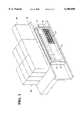
- FIG. 1is a perspective view of the EPL antenna and a circuit board with communication circuitry
- FIG. 2is a perspective view of the EPL antenna, the circuit board, and a display;
- FIG. 3is a perspective view of an EPL containing the components of FIG. 2;
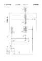
- FIG. 4is a circuit diagram of the EPL.
- electronic price label 10includes antenna 12, display 14 (FIG. 2), and printed circuit board 16.
- Antenna 12is an air dielectric Inverted-F antenna, implemented as a folded planar conductor 17.
- Antenna 12includes strip 18, top planar conductor 20, first side planar conductor 22, bottom planar conductor 24, second side planar conductor 26, and third side planar conductor 28.
- Strip 18extends from top planar conductor 20 and acts as an electrical link between top planar conductor 20 and printed circuit board 16, and maintains conductor 20 at a predetermined height above ground plane 24.
- Strip 18is generally L-shaped with the bottom end of strip 18 forming an antenna port 36 for passing a received signal to communication circuitry 30.
- Strip 18is about 6 mm in width, about 2.5 mm in length, and after the bend, about 4 mm in height.
- Strip 18leaves top planar conductor 20 perpendicularly at about 17 mm from end closest to conductor 22.
- Top planar conductor 20acts as a radiator of antenna 12.
- Top planar conductor 20is about 54 mm long by about 4 mm wide.
- Top planar conductor 20is oriented substantially perpendicularly to first side planar conductor 22.
- First side planar conductor 22is electrically connected or shorted to bottom planar conductor 24 and is oriented substantially perpendicularly at one end of bottom planar conductor 24.
- First side planar conductor 22maintains antenna 12 at a predetermined height above bottom planar conductor 24, and acts as a closed-end point of radiator top planar conductor 20.
- First side planar conductor 22is about 2.5 mm long by about 5 mm high.
- Bottom planar conductor 24acts as a ground plane of antenna 12 and is electrically connected to the common ground of communication circuitry 30 through ground strip 32. Bottom planar conductor 24 is substantially parallel to top planar conductor 20. Bottom planar conductor 24 is about 70 mm long by about 8 mm wide.
- Second and third side planar conductors 26 and 28extend from bottom planar conductor 24 and also act as corner reflectors which enhance the performance of antenna 12.
- Second side planar conductor 26is located at an opposite side of bottom planar conductor 24 from first side planar conductor 22. Since a shield effect against electric field disturbance from display 14 cannot be achieved by using only a flat ground plane, second side planar conductor 26 provides a shielding function against electromagnetic disturbance from display 14.
- Second side planar conductor 26is in close proximity to display 14 to provide more space for radiation around top planar conductor 20.
- Second side planar conductor 26is about 48 mm long by about 5 mm high.
- Third side planar conductor 28is located at an opposite end of bottom planar conductor 24 from first side planar conductor 22. Since antenna 12 has its electric field polarity along the "length" axis, a large extension of bottom planar conductor (ground plane) 24 in this direction, and toward the side of the open-end of top planar conductor 20, as much as possible, is desirable for better antenna performance. However, since EPL housing size is typically limited in the length direction, third side planar conductor 28 must be bent upwards from bottom planar conductor (ground plane) 24. This additional ground plane area provides better antenna performance. Third side planar conductor 28 is about 8 mm wide by about 5 mm high.
- Antenna 12has an operating frequency of about 2.45 GHz.
- Antenna 12uses the air gap between top planar conductor 20 and bottom planar conductor 24 as a dielectric.
- the length between the open end of top planar conductor 20 and strip 18 (about 37 mm) together with the height of first side planar conductor 22 (about 5 mm)determine the resonant frequency of antenna 12.
- top planar conductor 20 and strip 18determine the length between the closed end of top planar conductor 20 and strip 18 (about 17 mm), the length and height of first side planar conductor 22 (about 2.5 mm and 5 mm, respectively) and the length, width and height of strip 18 (about 2.5 mm, 6 mm, and 4 mm, respectively) determine the impedance of antenna port 36.
- top planar conductor 20determines bandwidth.
- antenna 12has an electric field polarity oriented along the length axis.
- Antenna 12may be fabricated from a stainless or cold-rolled steel to a thickness of about 0.2 mm. The steel is then bent, resulting in antenna 12 having the shape illustrated in FIG. 1.
- Printed circuit board 16has a thickness of about 1 mm.
- Communication circuitry 30is shown as a single element to simplify the drawings, but actually employs much of the area of printed circuit board 16.
- Communication circuitry 30is preferably wireless communication circuitry which operates using wireless backscatter communication techniques.
- Printed circuit board 16sits adjacent antenna 12. Since bottom planar conductor 24 acts as the ground plane, printed circuit board 16 area is minimized.
- Printed circuit board 16additionally includes power supply 34, which is preferably a battery.
- Strip 18connects to communication circuitry 30 through electrical traces 38 to form an antenna port 36 for antenna 12.
- Antenna port 36is a soldering pad on printed circuit board 16 and connects to electrical traces 38.
- printed circuit board 16includes only two solder points 80 and 82, point 80 at antenna port 36 and point 82 at ground strip 32.
- antenna 12, printed circuit board 16, and display 14 of electronic price label 10are shown.
- Electronic price label 10further includes housing 42 and overlay 44.
- Housing 42can be made smaller in height, to no more than about 7 mm to 9 mm, using antenna 12.
- Housing 42fits within a suitable mount on the edge of shelf 46 where items 48 are arranged.
- Overlay 44typically uses as much frontal surface area of housing 42 as is practical for displaying static information.
- a signal incident on antenna 12generates an RF voltage between antenna port 36 and bottom planar conductor 24.
- This RF voltageis resonated and detected by detector 60 in communication circuitry 30.
- Antenna 12is designed to have a port impedance that is inductive to conjugately match the capacitive impedance of detector 60.
- Communication circuitry 30includes detector 60, signal processing circuitry 62, microcontroller 64, and bias control circuit 66.
- Detector 60is preferably a Schottky barrier-type silicon diode. Detector 60 couples to data port 88 at the junction of capacitance 68 and capacitance 70.
- Capacitance 68is a quarter-wave transmission line or RF open-circuit stub or discrete capacitor component which shorts out the radio frequency signal after it is detected by detector 60.
- Capacitance 70is a discrete component between detector 60 and signal processing circuitry 62.
- a modulated RF signalis received by antenna 12. Because of the series resonance of antenna 12 and diode 60, all of the detected RF signal appears across capacitance 68. Capacitance 70 couples the resulting signal to signal processing circuitry 62. Signal processing circuitry 62 amplifies the detected RF signal and detects on/off keyed data bits in the amplified RF signal. Microcontroller 64 processes the data bits to generate data for display by display 14. Microcontroller 64 also controls bias circuit 66 which controls a bias current and impedance of detector 60.
- antenna 12reduces cost because it uses a smaller printed circuit board area by transferring its ground plane area from an expensive printed circuit board to a cheap sheet of metal. Also antenna 12 reduces component count of folded metal which enables less material handling cost. Assembly is also easier, since a single sheet of metal and only two solder points are necessary.
Landscapes
- Engineering & Computer Science (AREA)
- Computer Networks & Wireless Communication (AREA)
- Waveguide Aerials (AREA)
Abstract
Description
Claims (6)
Priority Applications (1)
| Application Number | Priority Date | Filing Date | Title |
|---|---|---|---|
| US09/383,550US6100850A (en) | 1999-08-26 | 1999-08-26 | Electronic price label antenna |
Applications Claiming Priority (1)
| Application Number | Priority Date | Filing Date | Title |
|---|---|---|---|
| US09/383,550US6100850A (en) | 1999-08-26 | 1999-08-26 | Electronic price label antenna |
Publications (1)
| Publication Number | Publication Date |
|---|---|
| US6100850Atrue US6100850A (en) | 2000-08-08 |
Family
ID=23513661
Family Applications (1)
| Application Number | Title | Priority Date | Filing Date |
|---|---|---|---|
| US09/383,550Expired - LifetimeUS6100850A (en) | 1999-08-26 | 1999-08-26 | Electronic price label antenna |
Country Status (1)
| Country | Link |
|---|---|
| US (1) | US6100850A (en) |
Cited By (22)
| Publication number | Priority date | Publication date | Assignee | Title |
|---|---|---|---|---|
| US6268831B1 (en)* | 2000-04-04 | 2001-07-31 | Ericsson Inc. | Inverted-f antennas with multiple planar radiating elements and wireless communicators incorporating same |
| WO2002039538A3 (en)* | 2000-10-20 | 2002-08-29 | Rangestar Wireless Inc | Compact antenna with multiple polarizations |
| US6577278B1 (en)* | 2001-12-29 | 2003-06-10 | Hon Hai Precision Ind. Co., Ltd. | Dual band antenna with bending structure |
| US20030124985A1 (en)* | 2001-04-11 | 2003-07-03 | Shin Hyo Sik | Multi-band antenna and notebook computer with built-in multi-band antenna |
| EP1249888A3 (en)* | 2001-04-11 | 2004-01-07 | Lg Electronics Inc. | Internal display-mounted antenna for mobile electronic equipment and mobile electronic equipment incorporating same |
| US6700544B2 (en) | 2002-02-05 | 2004-03-02 | Theodore R. Anderson | Near-field plasma reader |
| WO2004034507A2 (en) | 2002-10-10 | 2004-04-22 | Centurion Wireless Technologies, Inc. | Narrow width dual/tri ism band pifa for wireless applications |
| US20040135730A1 (en)* | 2003-01-06 | 2004-07-15 | Samsung Electronics Co., Ltd. | Portable computer |
| WO2006070233A1 (en) | 2004-12-31 | 2006-07-06 | Nokia Corporation | Internal multi-band antenna with planar strip elements |
| US20060285345A1 (en)* | 2005-06-20 | 2006-12-21 | Visteon Global Technologies, Inc. | Integrated antenna in display or lightbox |
| US7183981B1 (en)* | 2005-09-02 | 2007-02-27 | Arcadyan Technology Corporation | Monopole antenna |
| EP2026412A1 (en)* | 2007-08-14 | 2009-02-18 | Wistron NeWeb Corp. | Broadband antenna and an electronic device thereof |
| US20110187611A1 (en)* | 2010-02-02 | 2011-08-04 | Laird Technologies Ab | Antenna Device For A Radio Communication Device |
| EP2355241A1 (en)* | 2010-02-02 | 2011-08-10 | Laird Technologies AB | An antenna device for a radio communication device |
| CN102576928A (en)* | 2009-10-29 | 2012-07-11 | 莱尔德技术股份有限公司 | A metal cover for a radio communication device |
| USRE43699E1 (en) | 2002-02-05 | 2012-10-02 | Theodore R. Anderson | Reconfigurable scanner and RFID system using the scanner |
| KR101273745B1 (en)* | 2011-11-17 | 2013-06-12 | 삼성전기주식회사 | Electronic shelf lable tag |
| EP1886379A4 (en)* | 2005-05-12 | 2014-03-19 | Valtion Teknillinen | ANTENNA CONSTRUCTION TO THE EXAMPLE OF AN RFID TRANSPONDERSYSTEM |
| US8730044B2 (en) | 2002-01-09 | 2014-05-20 | Tyco Fire & Security Gmbh | Method of assigning and deducing the location of articles detected by multiple RFID antennae |
| US20140327592A1 (en)* | 2013-05-03 | 2014-11-06 | Fih (Hong Kong) Limited | Antenna structure and wireless communication device employing same |
| EP3392960A4 (en)* | 2015-12-15 | 2019-01-02 | LG Innotek Co., Ltd. | Electronic shelf label and antenna therefor |
| US20230383979A1 (en)* | 2020-10-14 | 2023-11-30 | Honeywell International Inc. | Building controller with antenna |
Citations (9)
| Publication number | Priority date | Publication date | Assignee | Title |
|---|---|---|---|---|
| US4002886A (en)* | 1975-06-20 | 1977-01-11 | Ronald Murl Sundelin | Electronic price display unit |
| US4500880A (en)* | 1981-07-06 | 1985-02-19 | Motorola, Inc. | Real time, computer-driven retail pricing display system |
| US4924363A (en)* | 1989-02-15 | 1990-05-08 | Dapopp Products Ltd. | Attention-attracting device for use beneath a display shelf |
| US5172314A (en)* | 1991-05-03 | 1992-12-15 | Electronic Retailing Systems International | Apparatus for communicating price changes including printer and display devices |
| US5394159A (en)* | 1993-11-02 | 1995-02-28 | At&T Corp. | Microstrip patch antenna with embedded detector |
| US5448226A (en)* | 1994-02-24 | 1995-09-05 | Electronic Retailing Systems International, Inc. | Shelf talker management system |
| US5598169A (en)* | 1995-03-24 | 1997-01-28 | Lucent Technologies Inc. | Detector and modulator circuits for passive microwave links |
| US5668560A (en)* | 1995-01-30 | 1997-09-16 | Ncr Corporation | Wireless electronic module |
| US5794211A (en)* | 1995-06-13 | 1998-08-11 | Ncr Corporation | EPL price verification system and method |
- 1999
- 1999-08-26USUS09/383,550patent/US6100850A/ennot_activeExpired - Lifetime
Patent Citations (9)
| Publication number | Priority date | Publication date | Assignee | Title |
|---|---|---|---|---|
| US4002886A (en)* | 1975-06-20 | 1977-01-11 | Ronald Murl Sundelin | Electronic price display unit |
| US4500880A (en)* | 1981-07-06 | 1985-02-19 | Motorola, Inc. | Real time, computer-driven retail pricing display system |
| US4924363A (en)* | 1989-02-15 | 1990-05-08 | Dapopp Products Ltd. | Attention-attracting device for use beneath a display shelf |
| US5172314A (en)* | 1991-05-03 | 1992-12-15 | Electronic Retailing Systems International | Apparatus for communicating price changes including printer and display devices |
| US5394159A (en)* | 1993-11-02 | 1995-02-28 | At&T Corp. | Microstrip patch antenna with embedded detector |
| US5448226A (en)* | 1994-02-24 | 1995-09-05 | Electronic Retailing Systems International, Inc. | Shelf talker management system |
| US5668560A (en)* | 1995-01-30 | 1997-09-16 | Ncr Corporation | Wireless electronic module |
| US5598169A (en)* | 1995-03-24 | 1997-01-28 | Lucent Technologies Inc. | Detector and modulator circuits for passive microwave links |
| US5794211A (en)* | 1995-06-13 | 1998-08-11 | Ncr Corporation | EPL price verification system and method |
Cited By (35)
| Publication number | Priority date | Publication date | Assignee | Title |
|---|---|---|---|---|
| US6268831B1 (en)* | 2000-04-04 | 2001-07-31 | Ericsson Inc. | Inverted-f antennas with multiple planar radiating elements and wireless communicators incorporating same |
| WO2002039538A3 (en)* | 2000-10-20 | 2002-08-29 | Rangestar Wireless Inc | Compact antenna with multiple polarizations |
| US6957085B2 (en) | 2001-04-11 | 2005-10-18 | Lg Electronics Inc | Internal display-mounted antenna for mobile electronic equipment and mobile electronic equipment incorporating same |
| US20030124985A1 (en)* | 2001-04-11 | 2003-07-03 | Shin Hyo Sik | Multi-band antenna and notebook computer with built-in multi-band antenna |
| EP1249888A3 (en)* | 2001-04-11 | 2004-01-07 | Lg Electronics Inc. | Internal display-mounted antenna for mobile electronic equipment and mobile electronic equipment incorporating same |
| US7072690B2 (en) | 2001-04-11 | 2006-07-04 | Lg Electronics Inc. | Multi-band antenna and notebook computer with built-in multi-band antenna |
| US6577278B1 (en)* | 2001-12-29 | 2003-06-10 | Hon Hai Precision Ind. Co., Ltd. | Dual band antenna with bending structure |
| US20030122717A1 (en)* | 2001-12-29 | 2003-07-03 | Chuck Hood | Dual band antenna with bending structure |
| US8730044B2 (en) | 2002-01-09 | 2014-05-20 | Tyco Fire & Security Gmbh | Method of assigning and deducing the location of articles detected by multiple RFID antennae |
| US6700544B2 (en) | 2002-02-05 | 2004-03-02 | Theodore R. Anderson | Near-field plasma reader |
| USRE43699E1 (en) | 2002-02-05 | 2012-10-02 | Theodore R. Anderson | Reconfigurable scanner and RFID system using the scanner |
| EP1576694A4 (en)* | 2002-10-10 | 2006-01-04 | Centurion Wireless Tech Inc | Narrow width dual/tri ism band pifa for wireless applications |
| WO2004034507A2 (en) | 2002-10-10 | 2004-04-22 | Centurion Wireless Technologies, Inc. | Narrow width dual/tri ism band pifa for wireless applications |
| US20040135730A1 (en)* | 2003-01-06 | 2004-07-15 | Samsung Electronics Co., Ltd. | Portable computer |
| US7170452B2 (en)* | 2003-01-06 | 2007-01-30 | Samsung Electronics Co., Ltd. | Portable computer |
| WO2006070233A1 (en) | 2004-12-31 | 2006-07-06 | Nokia Corporation | Internal multi-band antenna with planar strip elements |
| CN101258641A (en)* | 2004-12-31 | 2008-09-03 | 诺基亚公司 | Built-in multiband antenna with planar strip element |
| EP1886379A4 (en)* | 2005-05-12 | 2014-03-19 | Valtion Teknillinen | ANTENNA CONSTRUCTION TO THE EXAMPLE OF AN RFID TRANSPONDERSYSTEM |
| US20060285345A1 (en)* | 2005-06-20 | 2006-12-21 | Visteon Global Technologies, Inc. | Integrated antenna in display or lightbox |
| US7535426B2 (en) | 2005-06-20 | 2009-05-19 | Visteon Global Technologies, Inc. | Integrated antenna in display or lightbox |
| US20070052591A1 (en)* | 2005-09-02 | 2007-03-08 | Wen-Shin Chao | Monopole antenna |
| US7183981B1 (en)* | 2005-09-02 | 2007-02-27 | Arcadyan Technology Corporation | Monopole antenna |
| US20090046016A1 (en)* | 2007-08-14 | 2009-02-19 | Wistron Neweb Corp. | Broadband antenna and an electronic device thereof |
| US7742003B2 (en) | 2007-08-14 | 2010-06-22 | Wistron Neweb Corp. | Broadband antenna and an electronic device thereof |
| EP2026412A1 (en)* | 2007-08-14 | 2009-02-18 | Wistron NeWeb Corp. | Broadband antenna and an electronic device thereof |
| CN102576928A (en)* | 2009-10-29 | 2012-07-11 | 莱尔德技术股份有限公司 | A metal cover for a radio communication device |
| US20110187611A1 (en)* | 2010-02-02 | 2011-08-04 | Laird Technologies Ab | Antenna Device For A Radio Communication Device |
| EP2355241A1 (en)* | 2010-02-02 | 2011-08-10 | Laird Technologies AB | An antenna device for a radio communication device |
| CN102244315A (en)* | 2010-02-02 | 2011-11-16 | 莱尔德技术股份有限公司 | An antenna device for a radio communication device |
| KR101273745B1 (en)* | 2011-11-17 | 2013-06-12 | 삼성전기주식회사 | Electronic shelf lable tag |
| US20140327592A1 (en)* | 2013-05-03 | 2014-11-06 | Fih (Hong Kong) Limited | Antenna structure and wireless communication device employing same |
| EP3392960A4 (en)* | 2015-12-15 | 2019-01-02 | LG Innotek Co., Ltd. | Electronic shelf label and antenna therefor |
| JP2019505115A (en)* | 2015-12-15 | 2019-02-21 | エルジー イノテック カンパニー リミテッド | COMMUNICATION DEVICE AND ELECTRONIC DEVICE INCLUDING THE SAME |
| US10607512B2 (en) | 2015-12-15 | 2020-03-31 | Atec Ap Co., Ltd. | Communication device and electronic device comprising the same |
| US20230383979A1 (en)* | 2020-10-14 | 2023-11-30 | Honeywell International Inc. | Building controller with antenna |
Similar Documents
| Publication | Publication Date | Title |
|---|---|---|
| US6100850A (en) | Electronic price label antenna | |
| US6184834B1 (en) | Electronic price label antenna for electronic price labels of different sizes | |
| US5668560A (en) | Wireless electronic module | |
| EP2183709B1 (en) | Antenna systems for passive rfid tags | |
| US7446729B2 (en) | Loop antenna unit and radio communication medium processor | |
| US6097347A (en) | Wire antenna with stubs to optimize impedance for connecting to a circuit | |
| US5394159A (en) | Microstrip patch antenna with embedded detector | |
| KR101119991B1 (en) | Rfid tag with enhanced readability | |
| US5861854A (en) | Surface-mount antenna and a communication apparatus using the same | |
| US7323994B2 (en) | RFID tag | |
| US6028564A (en) | Wire antenna with optimized impedance for connecting to a circuit | |
| EP2071495B1 (en) | Wireless ic device | |
| US7743997B2 (en) | Handheld combination bar code and RFID reader with integrated electronics and antenna | |
| US6040806A (en) | Circular-polarization antenna | |
| JP2011501519A (en) | RFID patch antenna with coplanar reference ground and floating ground | |
| KR20110076811A (en) | Wireless tag | |
| US20220255232A1 (en) | Antenna structure and mobile device including the same | |
| US7378972B2 (en) | RFID tag | |
| WO2007029296A1 (en) | Rf tag and method for manufacturing rf tag | |
| US20050174296A1 (en) | Antenna and wireless communications device having antenna | |
| JP6602513B2 (en) | Antenna device | |
| US11217887B2 (en) | Antenna module | |
| KR100848560B1 (en) | Solid State Flat Antenna | |
| US20050253685A1 (en) | Electronic label antenna | |
| US20210083361A1 (en) | Wireless communication device |
Legal Events
| Date | Code | Title | Description |
|---|---|---|---|
| AS | Assignment | Owner name:NCR CORPORATION, OHIO Free format text:ASSIGNMENT OF ASSIGNORS INTEREST;ASSIGNOR:UTSUMI, YOSHITAKA;REEL/FRAME:010203/0667 Effective date:19990818 | |
| STCF | Information on status: patent grant | Free format text:PATENTED CASE | |
| FPAY | Fee payment | Year of fee payment:4 | |
| FPAY | Fee payment | Year of fee payment:8 | |
| SULP | Surcharge for late payment | Year of fee payment:7 | |
| FPAY | Fee payment | Year of fee payment:12 | |
| AS | Assignment | Owner name:JPMORGAN CHASE BANK, N.A., AS ADMINISTRATIVE AGENT, ILLINOIS Free format text:SECURITY AGREEMENT;ASSIGNORS:NCR CORPORATION;NCR INTERNATIONAL, INC.;REEL/FRAME:032034/0010 Effective date:20140106 Owner name:JPMORGAN CHASE BANK, N.A., AS ADMINISTRATIVE AGENT Free format text:SECURITY AGREEMENT;ASSIGNORS:NCR CORPORATION;NCR INTERNATIONAL, INC.;REEL/FRAME:032034/0010 Effective date:20140106 | |
| AS | Assignment | Owner name:JPMORGAN CHASE BANK, N.A., ILLINOIS Free format text:SECURITY AGREEMENT;ASSIGNORS:NCR CORPORATION;NCR INTERNATIONAL, INC.;REEL/FRAME:038646/0001 Effective date:20160331 | |
| AS | Assignment | Owner name:NCR VOYIX CORPORATION, GEORGIA Free format text:RELEASE OF PATENT SECURITY INTEREST;ASSIGNOR:JPMORGAN CHASE BANK, N.A., AS ADMINISTRATIVE AGENT;REEL/FRAME:065346/0531 Effective date:20231016 Owner name:BANK OF AMERICA, N.A., AS ADMINISTRATIVE AGENT, NORTH CAROLINA Free format text:SECURITY INTEREST;ASSIGNOR:NCR VOYIX CORPORATION;REEL/FRAME:065346/0168 Effective date:20231016 | |
| AS | Assignment | Owner name:NCR VOYIX CORPORATION, GEORGIA Free format text:CHANGE OF NAME;ASSIGNOR:NCR CORPORATION;REEL/FRAME:065820/0704 Effective date:20231013 |