US6100846A - Fixed patch array scanning antenna - Google Patents
Fixed patch array scanning antennaDownload PDFInfo
- Publication number
- US6100846A US6100846AUS09/265,278US26527899AUS6100846AUS 6100846 AUS6100846 AUS 6100846AUS 26527899 AUS26527899 AUS 26527899AUS 6100846 AUS6100846 AUS 6100846A
- Authority
- US
- United States
- Prior art keywords
- antenna
- laminate
- patches
- apertures
- waveguide
- Prior art date
- Legal status (The legal status is an assumption and is not a legal conclusion. Google has not performed a legal analysis and makes no representation as to the accuracy of the status listed.)
- Expired - Fee Related
Links
- 239000004020conductorSubstances0.000claimsabstractdescription46
- 230000033001locomotionEffects0.000claimsdescription16
- 230000000694effectsEffects0.000claimsdescription7
- 230000010363phase shiftEffects0.000abstractdescription7
- 238000004891communicationMethods0.000abstractdescription5
- 230000008878couplingEffects0.000description9
- 238000010168coupling processMethods0.000description9
- 238000005859coupling reactionMethods0.000description9
- 230000008901benefitEffects0.000description8
- 238000000034methodMethods0.000description7
- 229910000859α-FeInorganic materials0.000description4
- 230000033228biological regulationEffects0.000description3
- 238000003491arrayMethods0.000description2
- 239000000463materialSubstances0.000description2
- 238000012986modificationMethods0.000description2
- 230000004048modificationEffects0.000description2
- RYGMFSIKBFXOCR-UHFFFAOYSA-NCopperChemical compound[Cu]RYGMFSIKBFXOCR-UHFFFAOYSA-N0.000description1
- 238000004458analytical methodMethods0.000description1
- 230000003466anti-cipated effectEffects0.000description1
- 230000008859changeEffects0.000description1
- 230000001276controlling effectEffects0.000description1
- 229910052802copperInorganic materials0.000description1
- 239000010949copperSubstances0.000description1
- 238000013461designMethods0.000description1
- 238000001514detection methodMethods0.000description1
- 239000003989dielectric materialSubstances0.000description1
- 238000005530etchingMethods0.000description1
- 238000003780insertionMethods0.000description1
- 230000037431insertionEffects0.000description1
- 239000007788liquidSubstances0.000description1
- 238000004519manufacturing processMethods0.000description1
- 230000007246mechanismEffects0.000description1
- 230000001902propagating effectEffects0.000description1
- 230000001105regulatory effectEffects0.000description1
- 238000000926separation methodMethods0.000description1
- 239000007787solidSubstances0.000description1
- 239000000126substanceSubstances0.000description1
- 239000000758substrateSubstances0.000description1
- 238000012360testing methodMethods0.000description1
Images


Classifications
- H—ELECTRICITY
- H01—ELECTRIC ELEMENTS
- H01Q—ANTENNAS, i.e. RADIO AERIALS
- H01Q13/00—Waveguide horns or mouths; Slot antennas; Leaky-waveguide antennas; Equivalent structures causing radiation along the transmission path of a guided wave
- H01Q13/20—Non-resonant leaky-waveguide or transmission-line antennas; Equivalent structures causing radiation along the transmission path of a guided wave
- H01Q13/28—Non-resonant leaky-waveguide or transmission-line antennas; Equivalent structures causing radiation along the transmission path of a guided wave comprising elements constituting electric discontinuities and spaced in direction of wave propagation, e.g. dielectric elements or conductive elements forming artificial dielectric
- H—ELECTRICITY
- H01—ELECTRIC ELEMENTS
- H01Q—ANTENNAS, i.e. RADIO AERIALS
- H01Q1/00—Details of, or arrangements associated with, antennas
- H01Q1/36—Structural form of radiating elements, e.g. cone, spiral, umbrella; Particular materials used therewith
- H01Q1/38—Structural form of radiating elements, e.g. cone, spiral, umbrella; Particular materials used therewith formed by a conductive layer on an insulating support
- H—ELECTRICITY
- H01—ELECTRIC ELEMENTS
- H01Q—ANTENNAS, i.e. RADIO AERIALS
- H01Q21/00—Antenna arrays or systems
- H01Q21/06—Arrays of individually energised antenna units similarly polarised and spaced apart
- H01Q21/08—Arrays of individually energised antenna units similarly polarised and spaced apart the units being spaced along or adjacent to a rectilinear path
- H—ELECTRICITY
- H01—ELECTRIC ELEMENTS
- H01Q—ANTENNAS, i.e. RADIO AERIALS
- H01Q3/00—Arrangements for changing or varying the orientation or the shape of the directional pattern of the waves radiated from an antenna or antenna system
- H01Q3/12—Arrangements for changing or varying the orientation or the shape of the directional pattern of the waves radiated from an antenna or antenna system using mechanical relative movement between primary active elements and secondary devices of antennas or antenna systems
- H01Q3/14—Arrangements for changing or varying the orientation or the shape of the directional pattern of the waves radiated from an antenna or antenna system using mechanical relative movement between primary active elements and secondary devices of antennas or antenna systems for varying the relative position of primary active element and a refracting or diffracting device
Definitions
- This inventionrelates generally to scanning beam antennas and more particularly a fixed antenna that generates a scanning beam useful for radar and communication system applications.
- phase shifting antennasutilizing ferrite materials.
- One such phase shifting deviceis disclosed in U.S. Pat. No. 4,691,208. This device includes a ferrite plate surrounding a dielectric waveguide.
- ferrite phase shiftersare readily adaptable into antenna systems at microwave frequencies up to 20 GHz. Above that frequency, they are not particularly usable. Limitations of ferrite phase-shifting antennas include requiring a substantial power input to effect a phase change, high insertion loss, and requiring circuity not easy to integrate.
- Another scanning array antennais disclosed in U.S. Pat. No. 5,504,466.
- This antennauses a suspended dielectric and microstrip type microwave phase shifter. While this phase shifter can be easily integrated with other circuitry, there are substantial fabrication costs. These higher costs relate to needs for a large microwave laminate for the antenna substrate and special dielectric materials for the phase shifter. Also, this antenna is inefficient because of high circuit loss in the microstrip power splitter and phase shifter.
- An antenna of this inventionthat is particularly adapted to produce a scanning beam usable for radar and communication applications includes a frame. Attached to the support frame on an input side of the antenna is a reciprocating device that is operatively connected to a movable conductor. Spaced from the conductor is a conductive layer of a laminate. The laminate conductive layer is formed with a set of spaced apart, aligned apertures. These apertures than are covered by an elongated dielectric waveguide. The waveguide is attached to an outer surface of the laminate conductive layer and spaced from the movable conductor to form a uniform gap therebetween.
- a dielectric layerJoined to the conductive layer of the laminate on an input side of the antenna is a dielectric layer.
- a set of conducting patchesthat conductively align with the laminate conductive layer apertures.
- an electromagnetic waveis transmitted through the waveguide. This wave disseminates through the laminate conductive layer apertures to respectively energize the patches.
- Electromagnetic energy from the energized patchesthen combines to form an outward projecting, fan-shaped beam of radiated energy.
- This beamis positioned perpendicular to the plane of the laminate.
- the reflecting conductorreciprocates back and forth toward the dielectric waveguide to vary the uniform gap and produce a phase shift in the electromagnetic wave propagating in the waveguide.
- the phase shifting of the wavecauses the beam to scan left and right in alignment with the patches.
- the antenna of this inventionproduces several advantages over scanning antennas known or now in use.
- a first advantage of this inventive antennais that its operation requires minimal mechanical input. Structure producing this input is simple, inexpensive, and highly reliable. Any required service is easily performed by a semi-skilled technician.
- a second advantageis that the antenna structure is light weight and compact. This characteristic is particularly valuable where this inventive antenna is adapted for use in motor vehicles and aircraft radar systems.
- a third advantageis that structure of the antenna may be adapted to produce one-directional and two-directional scanning. Where used in a radar system, for example, detection capability may be tailored to the anticipated spacial positioning of the object to be detected.
- a fourth advantageis that the patches of antenna may be arranged in varying arrays to form different beam configurations.
- t he antennamay be adapted to operate at different frequencies for example in a range from one to one thousand GizaHerz.
- the antenna structuremay have different end uses in conformance with governmental regulation, such as published by the FCC.
- FIG. 1is a perspective view of an input side of an antenna of this invention shown without a reciprocating device.
- FIG. 2is an end elevational view of the antenna of FIG. 1 where the reciprocating device now is shown.
- FIG. 3is a perspective view of an output side of the antenna of FIG. 1.
- FIG . 3Ais a detailed plan view of a portion of a laminate of the antenna of FIG. 1 showing offsetting of apertures in the laminate.
- FIG. 4is a perspective view of an input side of a further antenna embodiment of this invention that again is shown without a reciprocating device.
- FIG. 5is an end elevational view of the antenna shown in FIG. 4.
- FIG. 6is a cross-sectional view as seen generally alone to line 6--6 in FIG. 4 showing one pair of patches.
- FIG. 7is a cross-sectional view as seen generally along the line 7--7 in FIG. 6.
- FIG. 8is a perspective view of an output side of the antenna of FIG. 4.
- FIG. 9is a plan view of an input side of an antenna similar to that in FIG. 4 but having a more extensive array of patches.
- FIG. 10is an end elevational view of the antenna of FIG. 9.
- FIG. 11is a perspective view of an output side of the antenna of FIG. 9.
- FIG. 12is a detailed plan view of a portion of the output side of the antenna of FIG. 9 as seen generally alone the line 12--12 of FIG. 11.
- FIG. 13is a perspective view of a rotating cam-type reflecting conductor to effect phase shifting.
- FIG. 14is a plan view of an input side on an antenna of this invention for scanning in two directions.
- FIG. 15is a side elevational view of a portion of the FIG. 14 antenna as seen generally along the line 15--15 in FIG. 14.
- FIG. 16is a perspective view of an output side of the antenna of FIG. 14.
- FIG. 17is a view showing a two-directional angular path of movement of a beam emitting from the FIG. 14 antenna.
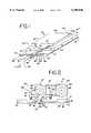
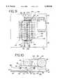
- FIGS. 1-3An antenna of this invention, particularly adapted for use in a vehicular radar system, is shown generally in FIGS. 1-3 and designated 10.
- the antenna 10includes a frame 12 that supported a laminate 16.
- the laminate 16includes a conductive layer 18 on an input side 20 of the antenna 10 and a dielectric layer 22 on a output side 24 of the antenna 10.
- first and second support plates 26, 27Attached to the frame 12 and projecting rearward on the antenna input side 20 are first and second support plates 26, 27. Attached to the first plate 26 is a motor 28 having a motor pulley 30. Mounted on the second plate 27 is an eccentric drive cam 32, a drive cam shaft 34, and a drive cam pulley 36. A belt 35 then connects the motor pulley 30 to the drive cam pulley 36.
- the drive cam 32is operatively attached to an outer side 37 of a reflecting conductive plate 38. Ends 39 of the reflecting conductive plate 38 are movably carried on guides 40 attached to the frame 12. As carried, a uniform space 42 is formed between an inner side 44 of the conductive plate 38 and an outer surface 46 of the laminate conductive layer 18. A uniform gap 43 then is formed between the inner side 44 of the plate 38 and a dielectric waveguide 50 carried on the laminate conductive layer outer surface 46.
- the laminate conductive layer 18is formed with a set of spaced apart, longitudinally align ed apertures 48.
- the preferred aperture configurationis rectangular.
- the waveguide 50covers the apertures 48.
- a setis a set of spaced apart, rectangular shaped patches 54.
- the preferred patch materialis copper.
- the patches 54are positioned so that a longitudinal axis L-L(P) of the patches 54 aligns with a longitudinal axis L-L(A) of the apertures 48 and a longitudinal axis L-L(W) of the waveguide 50.
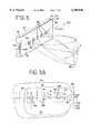
- an electromagnetic wave input EI(1)is introduced into an input end 56 of the waveguide 50. Because the antenna 10 is for vehicular use, the prescribed FCC wave frequency is 76.5 GHz.
- An appropriate electromagnetic wave mode launcher(not shown) may be required to connect the antenna input EI(1) to a source of energy, for example a solid state waveguide oscillator.
- the waveguide 50distributes this wave energy input EI(1) to the apertures 48 in the laminate conductive layer 18. Distribution of this wave energy EI is unequal. Control of the coupled energy through the apertures 48 is regulated to maximize energy radiated into the desired beam and minimize energy into undesired sidelobe beams in other directions. As may be better understood by viewing FIG. 3A, to effect these needed input differences the apertures 48 are individually laterally offset from the aperture axis L-L(A). As shown, the aperture 48a, which is closest to the input end 56 of the guidewave 50, is laterally offset from the aperture axis L-L(A) a distance d-2. The next closest aperture 48b is offset a lesser distance d-1.
- the next over aperture 48cis offset an even lesser distance d so that a center of the aperture 48c substantially aligns with the L-L(A) axis.
- An alternative method to vary energy couplingis to align the apertures 48 along the axis L-L(A) and then vary aperture dimensions.
- the now distributed wave energyenergizes the patches 54 by causing currents to flow on a surface of the patches 54.
- Electromagnetic energy radiated from the energized patches 54combines in space to form a beam 58 of radiated energy that projects outwardly from the antenna output side 24.
- the beam 58has a fan-like shape at a distance from the antenna 10.
- the beam 58is narrow in a plane aligning with the axis L-L(P) of the patches 54 and is wide in a plane perpendicular to that axis.
- the motor 28is energized to rotate the motor pulley 30 to drive the belt 35 and rotate drive cam shaft 34 and drive cam pulley 36.
- Resulting drive cam rotationcauses the reflecting conductive plate 39 to reciprocate back and forth toward the waveguide 50 to vary the gap 43.
- the plate guides 40insure that the gap 43 between the plate 38 and the waveguide 50 remains uniform. This movement of the plate 36 and thus variation of the gap 43 induces a phase shift in the electromagnetic wave input EI passing through the waveguide 50 and then to the patches 54.
- This phase shifting of the input EIcauses the beam 58 emitting from the patches 54 in the plane in which the fan-shaped beam 58 is narrow to scan back and forth as seen in FIG. 3.
- the arc of scanningdepends on the variation of the gap 43 and the corresponding phase shift induced in the electromagnetic wave input EI.
- Maximum beam scanningdepends on the frequency of the EI input, the dimensions and dielectric constant of the dielectric waveguide 50 as well as the dimensional variation of the gap 43.
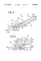
- FIGS. 4-8A further embodiment of this inventive antenna is shown generally in FIGS. 4-8 and designated 70. Where the structure of antenna 70 is like that of the antenna 10, like reference numbers are used.
- the antenna 70like the antenna 10, has a frame 12 to support a laminate 16.
- the laminate 16includes a conductive layer 18 on an input side 20 of the antenna 70 and a dielectric layer 22 on an output side 24 of the antenna 70.
- Attached to the frame 12 and projecting rearward on the antenna input side 20are support plates 26 and 27. Attached to the plate 26 is a motor 28 having a motor pulley 30. On the second plate 27 is mounted an eccentric drive cam 32, a drive cam shaft 34, and a drive cam pulley 36. The drive cam 32 is operatively attached to an outer side 37 of a reflecting conductive plate 38. Ends 39 of the reflecting conductive plate 38 are moveable carried on guides 40 attached to the frame 12. As carried, a uniform space 42 is formed between an inner side 44 of the conductive plate 38 and an outer surface 46 of the laminate of the laminate conductive layer 18. A uniform gap 43 then is formed between the plate inner side 44 and a dielectric waveguide 50 carried on the outer surface 46 of the laminate conductive layer 18.
- the laminate conductive layer 18is formed with a set of spaced apart, longitudinally aligned apertures 48.
- the preferred apertures configurationagain is rectangular.
- the waveguide 50covers the apertures 48 and is positioned so that the longitudinal axis L-L(W) of the waveguide 50 and a parallel longitudinal axis L-L(M) passing through centers of set of tree-shaped conducting microstrip lines or trees 82 are aligned.
- each laminate conductive layer aperture 48is vertically aligned with a trunk section 80 of one microstrip conducting distribution tree 82.
- the lines 82are attached to an outer surface 52 of the laminate dielectric layer 22 such that each aperture 48 in the laminate conductive layer in inwardly offset from an open end 84 of each tree trunk section 80 a distance equal to one-half the wavelength (of the wave in the microstrip line) at the frequency of an electromagnetic wave input EI(2) to the antenna 70.
- An outer end 86 of each tree trunk section 80connects with a pair of limb sections 88 that extend respectively outward from each side of the tree truck section 80.
- each tree limb section 88 of each tree 82Longitudinally offset from outer ends 90 of the tree limb sections 88 of each tree 82 is a pair of spaced apart conducting patches 92.
- the patches 92 of each pairare connected to the respective tree limb section outer ends 90 by a respective tree branch section 94.
- each patch pairconnecting with one microstrip tree 82.
- the patches 92 of each pairare arranged to define five columns 96 of patches 92 with the patches 92 of adjacent columns 96 then arranged to define a two rows 98 of patches 92.
- an electromagnetic wave input EI(2)is introduced into an input end 56 of the waveguide 50. Because the antenna 70 also is particularly adapted for vehicular use, the prescribed FCC wave frequency is 76.5 GHz.
- the waveguide 50distributes this wave energy input EI(2) to the apertures 48 in the laminate conductive layer 18.
- the now divided wave energy EI(2)then passes through the apertures 48 to the trunk section 80 of each microstrip distribution tree 82.
- the electromagnetic wave EI(2) portion in each trunk section 80again divides to energize each pair of patches 92 by passing through connecting tree limb sections 88 and branch sections 94.
- Radiated electromagnetic energy from the energized patches 94combines to form a beam 100 of radiated energy that projects outwardly from the output side 24 of the antenna 70.
- the beam 100is fan-shaped such that the beam 100 vertically is more broadly focused and horizontally is more narrowly focused.
- the motor 28Concurrent with the EI(2) wave input, the motor 28 is energized to rotate the drive cam 32. Cam rotation causes the reflecting conductive plate 38 to reciprocate back and forth toward the waveguide 50 to vary the gap 43.
- the plate guides 40insure that the gap 43 between the plate 38 and the waveguide 50 remains uniform over the length of the waveguide 50 during plate movement. Movement of the plate 38 induces a phase shift in the electromagnetic wave input EI(2) passing through the waveguide 50 and then to the patches 94 through the microstrip distribution trees 82.
- Phase shifting of the input EI(2)causes the beam 100 emitting from the patches 94 to scan back and forth in an arcuate shaped path 102.
- a plane of the path 102aligns with the axis L-L(M) of the microstrip lines 82.
- the beam 100may readily reflect from an object, for example another vehicle, 100 meters in front and 10 meters on each side of the antenna 70.
- the degree of arc spanningdepends on the variation of the gap 43 and corresponding phase shift induced in the electromagnetic wave EI(2).
- Maximum beam scanningdepends on the frequency of input EI(2), the dimensions and dielectric constant of the waveguide 50 as well the dimensional variations of the gap 43.
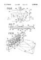
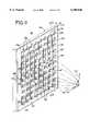
- FIGS. 9-12 and designated 108A still further embodiment of this inventive antenna is shown generally in FIGS. 9-12 and designated 108.
- the antenna 108includes operative rotating means 112 to effect phase shifting of an electromagnetic wave input EI(3) to the antenna 108.
- the antenna 108includes a frame 12. Attached to the frame 12 is a laminate 114 having an conductive layer 116 on the input side 110 of the antenna 108 and a dielectric layer 118 on an output side 120 of the antenna 108.
- the laminate conductive layer 116is formed with a set of spaced apart, rectangular apertures 122. Aligning with the apertures 112 and attached to an outer surface 124 of the laminate conductive layer 116 is a further elongated dielectric waveguide 126. End 128a, 128b of the waveguide 126 is pointed and contained in a channel-shaped conductive mode launcher 130. The launchers 130 in turn are respectively held by screws 132 secured in the frame 12. The launcher 130 at an input end 128a of the waveguide 126 allows connection of an electromagnetic source to the launcher 130.
- the launcher 130 at the opposite end 128b of the waveguide 126is primarily for test purposes to determine the small percent of energy reaching this end 128b of the dielectric waveguide 126. In practice this end launcher 130 may be removed.
- the pointed end 128b of the dielectric waveguide 126may be coated with a liquid absorbing substance to absorb energy and prevent unwanted energy reflection.
- each column 142is connected in parallel to a microstrip wave distribution tree 144.
- the trees 144are attached to the laminate dielectric layer outer surface 134. Because there are eight columns 142, there are eight (8) distribution trees 144.
- Each tree 144has a central trunk section 146 that aligns with one aperture 122 in the laminate conductive layer 116. As aligned, the respective apertures 122 are inwardly offset from an open end 148 of that tree trunk section 146.
- the dimension of the offsetis based on a frequency of an electromagnetic wave input EI(3) to the antenna 108.
- the offsetis one-quarter of the wavelength of the electromagnetic wave EI(3) which propagates in the microstrip tree trunk section 146.
- each tree trunk section 146connects with inner ends 152 of right and left aligned limb sections 154, 156.
- a set of ten spaced apart patches 138is connected one each to the limb sections 154, 156 of each tree 144 by a respective branch section 158.
- the limb sections 154, 156 of the eight (8) distribution tree 144are aligned parallel to each other but positioned perpendicular to a longitudinal axis L-L(W) of the waveguide 126.
- electromagnetic wave EI(3)is inputed into the end 128a of the dielectric wave guide 126.
- the wave frequencyis 76.5 GHz in accordance with FCC regulations.
- the waveguide 126distributes this wave energy input EI(3) to the apertures 122 in the laminate conductive layer 116. Distribution of the wave energy input EI(3) is unequal. Control of the coupled energy through the aperture 122 is done to maximize energy radiated into the desired beam and minimize energy radiated into undesired sidelobes beams in other directions.
- the apertures 122are individually offset respectively from an axis L-L(A) of the apertures 122.
- An alterative method to vary energy couplingis to align the apertures 122 along the L-L(A) axis but vary aperture dimensions.
- the now divided wave energy EI(3)then passes through the apertures 122 to the trunk section 146 of each microstrip distribution tree 144.
- the electromagnetic wave EI(3) in each trunk section 146again divides to energize the limb sections 154, 156 of that tree 144.
- the now further divided input wave EI(3)then flows through the branch sections 158 to the connecting patches 138 to energize the patch array 136 of eighty patches 138.
- other patch arrayscomprising different a different number of rows 140 and columns 142 may be used.
- the number of patches 138 in the rows 138 and columns 140is selected to achieve a desired beam angle in each of the planes of the beam. Available design procedures to determine beam angles are not affected by the use of aperture coupling in the laminate conductive layer 116, by the dielectric feed line method, nor by the phase shift scanning method.
- Electromagnetic energy from the energized patches 138combines to form a beam 160 of radiated energy that projects outwardly from the output side 120 of the antenna 108.
- the beam 160is both vertically and horizontally focused; the half-power beamwidth in each plane depends on the patch separation and the number of patches 138 in the rows 140 and columns 142.
- a motor 28 of the antenna 108is energized to rotate the phase-shifting device 112, see FIG. 10.
- the rotation of a drive cam 32 of the device 112 against an outer surface 37 of a movable conductor 38 of the device 112causes motion of the conductor 38 against springs 41 such that a gap 43 between the conductor 38 and the dielectric waveguide 126 of the antenna 108 is varied.
- Typical variation of this gap 43is from 0.001 to 0.050 in. to achieve typical beam scanning of 20 degrees in a plane of the dielectric waveguide 126.
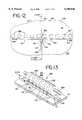
- An alternate method to achieve variation of the gap 43is to locate a rotating reflecting conductor cam device 162, shown typically in FIG. 13, directly over the dielectric waveguide 126.
- This cam device 162includes a conductor cam shaft 164 that is operatively connected to a conductor cam pulley, belt, and a motor pulley of a motor (not shown).
- Carried on the conductor cam shaft 164is a set of like-eccentrically positioned reflecting conductor cams 166.
- the conductor cams 166are separated by spaces 167 so that the conductor cams 166 locate between adjacent apertures 122 in the laminate conductive layer 116. As spaced apart, only seven conductor cams 166 are required for the eight apertures 122.
- the spaces 167 between the conductor cams 166align respectively with the apertures 122 to minimize the effect of the cam presence as the cams 166 rotate on the coupling of energy through the apertures 122.
- the conductor cams 166rotate to increase and decrease the gap 168 between the cams 166 and the waveguide 126, the conductor cams 166 induce a phase-shifting in the electromagnetic wave input EI(3) passing through the waveguide 126.
- the EI(3) wave input to the patches 138then likewise is shifted in phase causing the beam 160 emitting from the patches 138 to scan back and forth in an arcuate shaped path 170.
- the path 170 of beam movementremains substantially aligned with the waveguide axis L-L(W) and is proximately 20 degrees wide.
- the beam 160readily reflects from objects, for example other vehicles, a far as 100 meters in front and 10 meters on each side of the antenna 108 in front of the vehicle on which the antenna 108 is mounted.
- FIG. 14-16A two-directional antenna of this invention, capable of beam scanning in both planes of the array, is shown in FIG. 14-16 and designated 180.
- the antenna 180includes a frame 182. Positioned within the frame 182 is a laminate 183 having a conductive layer 184 positioned on an input side 186 of the antenna 180 and a dielectric layer 218 positioned on an output side 210 of the antenna 180.
- the laminate conductive layer 184is formed with four sets of spaced apart, aligned rectangular apertures 188. Each set of apertures 188 then is covered by a secondary dielectric waveguide 190 attached to an outer surface 192 of the laminate conductive layer 184.
- Each secondary waveguide 190is defined by an elongated portion 194 positioned over a respective set of the apertures 188 and a connecting arcuate portion 196 positioned in a border area 198 of the frame 182.
- a primary waveguide 202Located next and spaced from outermost points 200 of the waveguide arcuate portions 196 is a primary waveguide 202. As positioned, respective primary gaps 201, 203, 205, and 207 are formed between the primary waveguide 202 and the outermost points 200 of each arcuate portion 196 of the secondary waveguides 190. These primary gaps 201-207 are not the same. The size of the primary gaps 201-207 controls the percent coupling level of electromagnetic energy in the secondary waveguides 190. The benefit of controlling the percent coupling level in the secondary waveguides 190 is to maximize the energy in the desired beam of radiated energy from the antenna 180 and minimize the energy radiated into undesired sidelobes directions. Input end 204 of the primary waveguide 202 is carried in an channel of an electromagnetic wave mode launcher 206 secured to the frame 182 by screws 208.
- the output side 210 of the antenna 180is shown in detail in FIG. 16.
- the antenna output side 210includes a grid-like array 212 of conducting patches 214. These patches 214 are attached to an outer surface 216 of the dielectric layer 218 of the laminate 183.
- the patch array 212is defined by eight rows 220 and four columns 222 with the rows 220 and columns 222 with the rows 220 and the columns 222 positioned perpendicular.
- the patches 214 in respective columns 222are located to align with the apertures 188 covered by the respective waveguides 190.
- the rectangular apertures 188are of like size along the length of the conducting plane under the secondary dielectric wave guides 190. However, it is desirable to control the percent of energy which couples through the apertures 188 from the secondary waveguides 190. This control (reduced percentage) is obtained by moving the center of the aperture 188 laterally from the center axis of the apertures 188 which is parallel to the axis of the patches 214. Standard analysis is used to compute the desired percent coupling value for each of the nine apertures 188 and also how far to displace the center of the aperture 188 from the center of the secondary dielectric waveguide 190 to obtain the desired percent coupling for each of the apertures 188.
- the antenna 180is operated by introducing an electromagnetic wave EI(4) into the input end 204 of the primary dielectric waveguide 202.
- the frequency of the energy input EI(4)is 76.5 GHz in accordance with FCC regulations.
- the primary waveguide 202distributes this wave energy input EI(4) in a non-uniform manner through the coupling gaps 201-207 to the arcuate portions 196 of the secondary waveguides 190.
- the now divided wave energy EL(4)then flows through the elongated portion 194 of each secondary waveguide 190 and into the respective laminate conductive layer apertures 188 to energize the patches 214 respectively aligned with those apertures 188.
- Electromagnetic energy emitting from the now energized patches 214combines to form a beam 226 of radiated energy that projects outwardly from the output side 210 of the antenna 180.
- the beam 226is essentially pencil-shaped that typically will have differing (half-power) beam angles in the two planes. In this case, because there are more patches 214 in the direction of the columns 222, the beam angle in the vertical plane will be smaller than in the perpendicular (horizontal) plane of rows 220.
- a primary motor 228 carried by the antenna 180 on its input side 186is energized.
- An output shaft 230 of the primary motor 228is operatively connected to a primary conductor cam drive shaft 232. Ends of the shaft 232 are carried by bearing supports 236.
- the conductor cam drive shaft 232is positioned parallel to and directly over the primary waveguide 202.
- On the primary conductor cam drive shaft 232is a set of three spaced apart reflecting conductor cams 238 placed to align with and be spaced respectively between the outermost points 200 of secondary waveguide arcuate portions 196. As located, a primary gap 240 is formed between each conductor cam 238 and a top surface of the primary waveguide 202.
- a secondary motor 248 carried on the input side 186 of the antenna 180is energized.
- An output shaft 230 of the secondary motor 248is operatively connected to a secondary cam drive shaft 250 having ends carried by a further pair of bearing supports 236. Spaced between these bearing supports 236 is a set of drive cams 252 operatively connected to a reflecting conductor plate 254.
- the plate 254is spaced from the secondary wave guides elongated portions 194 to form a secondary uniform gap 256 therebetween, see FIG. 15.
- the reflecting conductor plate 254moves back and forth toward the secondary wave guide elongated portions 194 to increase and decrease the secondary gap 256.
- This plate movementinduces a secondary phase-shifting in the energy wave input EI(4) passing through the waveguide elongated portions 194 and then to the patches 214. Because of this secondary phase-shifting input to the patches 214, the electromagnetic energy emitting from the patches 214 then combines to cause the beam 226 to scan up-and-down in an arcuate path of movement 258, see FIG. 16.
- the paths of movement 242, 258form a combined path of beam movement 260 shown typically in FIG. 17.
- the path 260 of the beam 226is in vertical and horizontal directions may be controlled by adjusting the rotational velocity of the motors 228, 248.
- the scanning beam 226may readily reflect from objects, for example another object or vehicle as far as 100 meters in front, 10 meters on each side, and 10 meters above and below the object or vehicle on which a radar system including the antenna 180 is mounted.
Landscapes
- Variable-Direction Aerials And Aerial Arrays (AREA)
- Waveguide Aerials (AREA)
Abstract
Description
1. Field of the Invention
This invention relates generally to scanning beam antennas and more particularly a fixed antenna that generates a scanning beam useful for radar and communication system applications.
2. Prior Art
Known scanning antennas heretofore included phase shifting antennas utilizing ferrite materials. One such phase shifting device is disclosed in U.S. Pat. No. 4,691,208. This device includes a ferrite plate surrounding a dielectric waveguide.
Generally, ferrite phase shifters are readily adaptable into antenna systems at microwave frequencies up to 20 GHz. Above that frequency, they are not particularly usable. Limitations of ferrite phase-shifting antennas include requiring a substantial power input to effect a phase change, high insertion loss, and requiring circuity not easy to integrate.
An electronic scanning antenna is shown in U.S. Pat. No. 4,667,201. While this antenna provides a wide range of scanning angles, its phase shifter is expensive especially in millimeter wave frequencies.
Another scanning array antenna is described in a paper authored by M-Y Li, S. Kanamalura, and K. Chang, entitled, Aperture-Coupled Microstrip Antenna Array Fed By Dielectric Image Line, and published in Electronics Letters, pp. 1105-1106, Vol. 30, No. Jul. 14, 1994. Structure of the discussed antenna is quite simple. In this case, the required phase shifting is effected by operating at different frequencies. Frequency scanning antennas have several limitations, however. First, the frequency bandwidth must be quite wide to obtain an effective scanning angle range. However, the needed frequency bandwidth may not comply with frequency bandwidth uses established by the Federal Communication Commission (FCC). Secondly, frequency scanning antennas cannot be used with radar or communication systems utilizing frequency modulation mechanisms.
Another scanning array antenna is disclosed in U.S. Pat. No. 5,504,466. This antenna uses a suspended dielectric and microstrip type microwave phase shifter. While this phase shifter can be easily integrated with other circuitry, there are substantial fabrication costs. These higher costs relate to needs for a large microwave laminate for the antenna substrate and special dielectric materials for the phase shifter. Also, this antenna is inefficient because of high circuit loss in the microstrip power splitter and phase shifter.
An antenna of this invention that is particularly adapted to produce a scanning beam usable for radar and communication applications includes a frame. Attached to the support frame on an input side of the antenna is a reciprocating device that is operatively connected to a movable conductor. Spaced from the conductor is a conductive layer of a laminate. The laminate conductive layer is formed with a set of spaced apart, aligned apertures. These apertures than are covered by an elongated dielectric waveguide. The waveguide is attached to an outer surface of the laminate conductive layer and spaced from the movable conductor to form a uniform gap therebetween.
Joined to the conductive layer of the laminate on an input side of the antenna is a dielectric layer. On an outer surface of the laminate dielectric layer is a set of conducting patches that conductively align with the laminate conductive layer apertures.
For use, an electromagnetic wave is transmitted through the waveguide. This wave disseminates through the laminate conductive layer apertures to respectively energize the patches.
Electromagnetic energy from the energized patches then combines to form an outward projecting, fan-shaped beam of radiated energy. This beam is positioned perpendicular to the plane of the laminate. Concurrent with energizing the patches, the reflecting conductor reciprocates back and forth toward the dielectric waveguide to vary the uniform gap and produce a phase shift in the electromagnetic wave propagating in the waveguide. The phase shifting of the wave causes the beam to scan left and right in alignment with the patches.
The antenna of this invention produces several advantages over scanning antennas known or now in use.
A first advantage of this inventive antenna is that its operation requires minimal mechanical input. Structure producing this input is simple, inexpensive, and highly reliable. Any required service is easily performed by a semi-skilled technician.
A second advantage is that the antenna structure is light weight and compact. This characteristic is particularly valuable where this inventive antenna is adapted for use in motor vehicles and aircraft radar systems.
A third advantage is that structure of the antenna may be adapted to produce one-directional and two-directional scanning. Where used in a radar system, for example, detection capability may be tailored to the anticipated spacial positioning of the object to be detected.
A fourth advantage is that the patches of antenna may be arranged in varying arrays to form different beam configurations.
Lastly, by changing the size of the patches and the configuration of the dielectric waveguide for example, t he antenna may be adapted to operate at different frequencies for example in a range from one to one thousand GizaHerz. Thus, the antenna structure may have different end uses in conformance with governmental regulation, such as published by the FCC.
FIG. 1 is a perspective view of an input side of an antenna of this invention shown without a reciprocating device.
FIG. 2 is an end elevational view of the antenna of FIG. 1 where the reciprocating device now is shown.
FIG. 3 is a perspective view of an output side of the antenna of FIG. 1.
FIG . 3A is a detailed plan view of a portion of a laminate of the antenna of FIG. 1 showing offsetting of apertures in the laminate.
FIG. 4 is a perspective view of an input side of a further antenna embodiment of this invention that again is shown without a reciprocating device.
FIG. 5 is an end elevational view of the antenna shown in FIG. 4.
FIG. 6 is a cross-sectional view as seen generally alone toline 6--6 in FIG. 4 showing one pair of patches.
FIG. 7 is a cross-sectional view as seen generally along theline 7--7 in FIG. 6.
FIG. 8 is a perspective view of an output side of the antenna of FIG. 4.
FIG. 9 is a plan view of an input side of an antenna similar to that in FIG. 4 but having a more extensive array of patches.
FIG. 10 is an end elevational view of the antenna of FIG. 9.
FIG. 11 is a perspective view of an output side of the antenna of FIG. 9.
FIG. 12 is a detailed plan view of a portion of the output side of the antenna of FIG. 9 as seen generally alone theline 12--12 of FIG. 11.
FIG. 13 is a perspective view of a rotating cam-type reflecting conductor to effect phase shifting.
FIG. 14 is a plan view of an input side on an antenna of this invention for scanning in two directions.
FIG. 15 is a side elevational view of a portion of the FIG. 14 antenna as seen generally along theline 15--15 in FIG. 14.
FIG. 16 is a perspective view of an output side of the antenna of FIG. 14.
FIG. 17 is a view showing a two-directional angular path of movement of a beam emitting from the FIG. 14 antenna.
An antenna of this invention, particularly adapted for use in a vehicular radar system, is shown generally in FIGS. 1-3 and designated 10. Theantenna 10 includes aframe 12 that supported a laminate 16. The laminate 16 includes aconductive layer 18 on aninput side 20 of theantenna 10 and adielectric layer 22 on aoutput side 24 of theantenna 10.
Attached to theframe 12 and projecting rearward on theantenna input side 20 are first andsecond support plates first plate 26 is amotor 28 having amotor pulley 30. Mounted on thesecond plate 27 is aneccentric drive cam 32, adrive cam shaft 34, and adrive cam pulley 36. Abelt 35 then connects themotor pulley 30 to thedrive cam pulley 36. Thedrive cam 32 is operatively attached to anouter side 37 of a reflectingconductive plate 38. Ends 39 of the reflectingconductive plate 38 are movably carried onguides 40 attached to theframe 12. As carried, auniform space 42 is formed between aninner side 44 of theconductive plate 38 and anouter surface 46 of the laminateconductive layer 18. Auniform gap 43 then is formed between theinner side 44 of theplate 38 and adielectric waveguide 50 carried on the laminate conductive layerouter surface 46.
As best seen in FIGS. 1 and 2, the laminateconductive layer 18 is formed with a set of spaced apart, longitudinally aligned apertures 48. The preferred aperture configuration is rectangular. As attached to the laminate conductive layer outer surf ace 46, thewaveguide 50 covers theapertures 48.
Then, as best seen in FIGS. 2 and 3, formed by etching away aconducting layer 49 and anouter surface 52 of thelaminate dielectric layer 22 is a set is a set of spaced apart, rectangular shapedpatches 54. The preferred patch material is copper. Thepatches 54 are positioned so that a longitudinal axis L-L(P) of thepatches 54 aligns with a longitudinal axis L-L(A) of theapertures 48 and a longitudinal axis L-L(W) of thewaveguide 50.
During operation of theantenna 10, an electromagnetic wave input EI(1) is introduced into aninput end 56 of thewaveguide 50. Because theantenna 10 is for vehicular use, the prescribed FCC wave frequency is 76.5 GHz. An appropriate electromagnetic wave mode launcher (not shown) may be required to connect the antenna input EI(1) to a source of energy, for example a solid state waveguide oscillator.
Thewaveguide 50 distributes this wave energy input EI(1) to theapertures 48 in the laminateconductive layer 18. Distribution of this wave energy EI is unequal. Control of the coupled energy through theapertures 48 is regulated to maximize energy radiated into the desired beam and minimize energy into undesired sidelobe beams in other directions. As may be better understood by viewing FIG. 3A, to effect these needed input differences theapertures 48 are individually laterally offset from the aperture axis L-L(A). As shown, the aperture 48a, which is closest to theinput end 56 of theguidewave 50, is laterally offset from the aperture axis L-L(A) a distance d-2. The nextclosest aperture 48b is offset a lesser distance d-1. The next overaperture 48c is offset an even lesser distance d so that a center of theaperture 48c substantially aligns with the L-L(A) axis. An alternative method to vary energy coupling is to align theapertures 48 along the axis L-L(A) and then vary aperture dimensions.
The now distributed wave energy energizes thepatches 54 by causing currents to flow on a surface of thepatches 54. Electromagnetic energy radiated from the energizedpatches 54 combines in space to form abeam 58 of radiated energy that projects outwardly from theantenna output side 24. As seen in FIG. 3, thebeam 58 has a fan-like shape at a distance from theantenna 10. Thebeam 58 is narrow in a plane aligning with the axis L-L(P) of thepatches 54 and is wide in a plane perpendicular to that axis.
At the same time, themotor 28 is energized to rotate themotor pulley 30 to drive thebelt 35 and rotatedrive cam shaft 34 and drivecam pulley 36. Resulting drive cam rotation causes the reflectingconductive plate 39 to reciprocate back and forth toward thewaveguide 50 to vary thegap 43. The plate guides 40 insure that thegap 43 between theplate 38 and thewaveguide 50 remains uniform. This movement of theplate 36 and thus variation of thegap 43 induces a phase shift in the electromagnetic wave input EI passing through thewaveguide 50 and then to thepatches 54.
This phase shifting of the input EI causes thebeam 58 emitting from thepatches 54 in the plane in which the fan-shapedbeam 58 is narrow to scan back and forth as seen in FIG. 3. The arc of scanning depends on the variation of thegap 43 and the corresponding phase shift induced in the electromagnetic wave input EI. Maximum beam scanning depends on the frequency of the EI input, the dimensions and dielectric constant of thedielectric waveguide 50 as well as the dimensional variation of thegap 43.
A further embodiment of this inventive antenna is shown generally in FIGS. 4-8 and designated 70. Where the structure ofantenna 70 is like that of theantenna 10, like reference numbers are used.
Theantenna 70, like theantenna 10, has aframe 12 to support a laminate 16. Again, the laminate 16 includes aconductive layer 18 on aninput side 20 of theantenna 70 and adielectric layer 22 on anoutput side 24 of theantenna 70.
Attached to theframe 12 and projecting rearward on theantenna input side 20 aresupport plates plate 26 is amotor 28 having amotor pulley 30. On thesecond plate 27 is mounted aneccentric drive cam 32, adrive cam shaft 34, and adrive cam pulley 36. Thedrive cam 32 is operatively attached to anouter side 37 of a reflectingconductive plate 38. Ends 39 of the reflectingconductive plate 38 are moveable carried onguides 40 attached to theframe 12. As carried, auniform space 42 is formed between aninner side 44 of theconductive plate 38 and anouter surface 46 of the laminate of the laminateconductive layer 18. Auniform gap 43 then is formed between the plateinner side 44 and adielectric waveguide 50 carried on theouter surface 46 of the laminateconductive layer 18.
As shown in FIGS. 4 and 5, the laminateconductive layer 18 is formed with a set of spaced apart, longitudinally alignedapertures 48. The preferred apertures configuration again is rectangular. As attached to the laminate conductive layerouter surface 46, thewaveguide 50 covers theapertures 48 and is positioned so that the longitudinal axis L-L(W) of thewaveguide 50 and a parallel longitudinal axis L-L(M) passing through centers of set of tree-shaped conducting microstrip lines ortrees 82 are aligned.
Now referring to FIGS. 6 and 7, each laminateconductive layer aperture 48 is vertically aligned with atrunk section 80 of one microstrip conductingdistribution tree 82. Thelines 82 are attached to anouter surface 52 of thelaminate dielectric layer 22 such that eachaperture 48 in the laminate conductive layer in inwardly offset from anopen end 84 of each tree trunk section 80 a distance equal to one-half the wavelength (of the wave in the microstrip line) at the frequency of an electromagnetic wave input EI(2) to theantenna 70. Anouter end 86 of eachtree trunk section 80 connects with a pair oflimb sections 88 that extend respectively outward from each side of thetree truck section 80. Longitudinally offset fromouter ends 90 of thetree limb sections 88 of eachtree 82 is a pair of spaced apart conductingpatches 92. Thepatches 92 of each pair are connected to the respective tree limb section outer ends 90 by a respectivetree branch section 94.
As seen in FIG. 8, there are multiple pairs of patches 92 (in this case five such pairs) with each patch pair connecting with onemicrostrip tree 82. Thepatches 92 of each pair are arranged to define fivecolumns 96 ofpatches 92 with thepatches 92 ofadjacent columns 96 then arranged to define a tworows 98 ofpatches 92.
During operation of theantenna 70, an electromagnetic wave input EI(2) is introduced into aninput end 56 of thewaveguide 50. Because theantenna 70 also is particularly adapted for vehicular use, the prescribed FCC wave frequency is 76.5 GHz. Thewaveguide 50 distributes this wave energy input EI(2) to theapertures 48 in the laminateconductive layer 18.
The now divided wave energy EI(2) then passes through theapertures 48 to thetrunk section 80 of eachmicrostrip distribution tree 82. The electromagnetic wave EI(2) portion in eachtrunk section 80 again divides to energize each pair ofpatches 92 by passing through connectingtree limb sections 88 andbranch sections 94. Radiated electromagnetic energy from the energizedpatches 94 combines to form abeam 100 of radiated energy that projects outwardly from theoutput side 24 of theantenna 70. As seen in FIG. 8, at a distance from theantenna 70 thebeam 100 is fan-shaped such that thebeam 100 vertically is more broadly focused and horizontally is more narrowly focused.
Concurrent with the EI(2) wave input, themotor 28 is energized to rotate thedrive cam 32. Cam rotation causes the reflectingconductive plate 38 to reciprocate back and forth toward thewaveguide 50 to vary thegap 43. The plate guides 40 insure that thegap 43 between theplate 38 and thewaveguide 50 remains uniform over the length of thewaveguide 50 during plate movement. Movement of theplate 38 induces a phase shift in the electromagnetic wave input EI(2) passing through thewaveguide 50 and then to thepatches 94 through themicrostrip distribution trees 82. Phase shifting of the input EI(2) causes thebeam 100 emitting from thepatches 94 to scan back and forth in an arcuateshaped path 102. A plane of thepath 102 aligns with the axis L-L(M) of the microstrip lines 82. When theantenna 70 is scanning, thebeam 100 may readily reflect from an object, for example another vehicle, 100 meters in front and 10 meters on each side of theantenna 70.
The degree of arc spanning depends on the variation of thegap 43 and corresponding phase shift induced in the electromagnetic wave EI(2). Maximum beam scanning depends on the frequency of input EI(2), the dimensions and dielectric constant of thewaveguide 50 as well the dimensional variations of thegap 43.
A still further embodiment of this inventive antenna is shown generally in FIGS. 9-12 and designated 108. As seen in FIG. 9 and 10, theantenna 108 includes operative rotating means 112 to effect phase shifting of an electromagnetic wave input EI(3) to theantenna 108.
Similar to theantennas antenna 108 includes aframe 12. Attached to theframe 12 is a laminate 114 having anconductive layer 116 on theinput side 110 of theantenna 108 and adielectric layer 118 on anoutput side 120 of theantenna 108.
As seen in FIGS. 9 and 10, the laminateconductive layer 116 is formed with a set of spaced apart,rectangular apertures 122. Aligning with theapertures 112 and attached to anouter surface 124 of the laminateconductive layer 116 is a further elongateddielectric waveguide 126.End 128a, 128b of thewaveguide 126 is pointed and contained in a channel-shapedconductive mode launcher 130. Thelaunchers 130 in turn are respectively held byscrews 132 secured in theframe 12. Thelauncher 130 at an input end 128a of thewaveguide 126 allows connection of an electromagnetic source to thelauncher 130. Thelauncher 130 at theopposite end 128b of thewaveguide 126 is primarily for test purposes to determine the small percent of energy reaching thisend 128b of thedielectric waveguide 126. In practice thisend launcher 130 may be removed. Thepointed end 128b of thedielectric waveguide 126 may be coated with a liquid absorbing substance to absorb energy and prevent unwanted energy reflection.
As then best seen in FIGS. 9, 11 and 12 on anouter surface 134 of thelaminate dielectric layer 118 on theoutput side 120 of theantenna 108 is a grid-like array 136 of spaced apartpatches 138. There are eightypatches 138 arranged in tenparallel rows 140 and eight (8)parallel columns 142. Therows 140 andcolumns 144 are positioned perpendicular.
Thepatches 138 in eachcolumn 142 are connected in parallel to a microstripwave distribution tree 144. Thetrees 144 are attached to the laminate dielectric layerouter surface 134. Because there are eightcolumns 142, there are eight (8)distribution trees 144. Eachtree 144 has acentral trunk section 146 that aligns with oneaperture 122 in the laminateconductive layer 116. As aligned, therespective apertures 122 are inwardly offset from anopen end 148 of thattree trunk section 146. The dimension of the offset is based on a frequency of an electromagnetic wave input EI(3) to theantenna 108. The offset is one-quarter of the wavelength of the electromagnetic wave EI(3) which propagates in the microstriptree trunk section 146. An oppositeopen end 150 of eachtree trunk section 146 then connects withinner ends 152 of right and left alignedlimb sections patches 138 is connected one each to thelimb sections tree 144 by arespective branch section 158. As seen in FIGS. 9 and 12, thelimb sections distribution tree 144 are aligned parallel to each other but positioned perpendicular to a longitudinal axis L-L(W) of thewaveguide 126.
To operate theantenna 108, electromagnetic wave EI(3) is inputed into the end 128a of thedielectric wave guide 126. Again, theantenna 108 being for vehicular use, the wave frequency is 76.5 GHz in accordance with FCC regulations. Thewaveguide 126 distributes this wave energy input EI(3) to theapertures 122 in the laminateconductive layer 116. Distribution of the wave energy input EI(3) is unequal. Control of the coupled energy through theaperture 122 is done to maximize energy radiated into the desired beam and minimize energy radiated into undesired sidelobes beams in other directions. As discussed above, to effect these needed input differences, theapertures 122 are individually offset respectively from an axis L-L(A) of theapertures 122. An alterative method to vary energy coupling is to align theapertures 122 along the L-L(A) axis but vary aperture dimensions.
The now divided wave energy EI(3) then passes through theapertures 122 to thetrunk section 146 of eachmicrostrip distribution tree 144. The electromagnetic wave EI(3) in eachtrunk section 146 again divides to energize thelimb sections tree 144. The now further divided input wave EI(3) then flows through thebranch sections 158 to the connectingpatches 138 to energize thepatch array 136 of eightypatches 138. It should be understood that other patch arrays comprising different a different number ofrows 140 andcolumns 142 may be used. In general, the number ofpatches 138 in therows 138 andcolumns 140 is selected to achieve a desired beam angle in each of the planes of the beam. Available design procedures to determine beam angles are not affected by the use of aperture coupling in the laminateconductive layer 116, by the dielectric feed line method, nor by the phase shift scanning method.
Electromagnetic energy from the energizedpatches 138 combines to form abeam 160 of radiated energy that projects outwardly from theoutput side 120 of theantenna 108. As seen in FIG. 11, thebeam 160 is both vertically and horizontally focused; the half-power beamwidth in each plane depends on the patch separation and the number ofpatches 138 in therows 140 andcolumns 142.
Concurrent with the EI(3) wave input, amotor 28 of theantenna 108 is energized to rotate the phase-shiftingdevice 112, see FIG. 10. The rotation of adrive cam 32 of thedevice 112 against anouter surface 37 of amovable conductor 38 of thedevice 112 causes motion of theconductor 38 againstsprings 41 such that agap 43 between theconductor 38 and thedielectric waveguide 126 of theantenna 108 is varied. Typical variation of thisgap 43 is from 0.001 to 0.050 in. to achieve typical beam scanning of 20 degrees in a plane of thedielectric waveguide 126.
An alternate method to achieve variation of thegap 43 is to locate a rotating reflectingconductor cam device 162, shown typically in FIG. 13, directly over thedielectric waveguide 126. Thiscam device 162 includes aconductor cam shaft 164 that is operatively connected to a conductor cam pulley, belt, and a motor pulley of a motor (not shown). Carried on theconductor cam shaft 164 is a set of like-eccentrically positioned reflectingconductor cams 166. Theconductor cams 166 are separated byspaces 167 so that theconductor cams 166 locate betweenadjacent apertures 122 in the laminateconductive layer 116. As spaced apart, only sevenconductor cams 166 are required for the eightapertures 122. Thespaces 167 between theconductor cams 166 align respectively with theapertures 122 to minimize the effect of the cam presence as thecams 166 rotate on the coupling of energy through theapertures 122.
As theconductor cams 166 rotate to increase and decrease the gap 168 between thecams 166 and thewaveguide 126, theconductor cams 166 induce a phase-shifting in the electromagnetic wave input EI(3) passing through thewaveguide 126. The EI(3) wave input to thepatches 138 then likewise is shifted in phase causing thebeam 160 emitting from thepatches 138 to scan back and forth in an arcuateshaped path 170. Thepath 170 of beam movement remains substantially aligned with the waveguide axis L-L(W) and is proximately 20 degrees wide. When theantenna 108 is scanning, thebeam 160 readily reflects from objects, for example other vehicles, a far as 100 meters in front and 10 meters on each side of theantenna 108 in front of the vehicle on which theantenna 108 is mounted.
A two-directional antenna of this invention, capable of beam scanning in both planes of the array, is shown in FIG. 14-16 and designated 180. As seen in FIG. 14, theantenna 180 includes aframe 182. Positioned within theframe 182 is a laminate 183 having aconductive layer 184 positioned on aninput side 186 of theantenna 180 and adielectric layer 218 positioned on anoutput side 210 of theantenna 180. The laminateconductive layer 184 is formed with four sets of spaced apart, alignedrectangular apertures 188. Each set ofapertures 188 then is covered by a secondarydielectric waveguide 190 attached to anouter surface 192 of the laminateconductive layer 184.
Eachsecondary waveguide 190 is defined by anelongated portion 194 positioned over a respective set of theapertures 188 and a connectingarcuate portion 196 positioned in aborder area 198 of theframe 182.
Located next and spaced fromoutermost points 200 of the waveguidearcuate portions 196 is aprimary waveguide 202. As positioned, respectiveprimary gaps primary waveguide 202 and theoutermost points 200 of eacharcuate portion 196 of thesecondary waveguides 190. These primary gaps 201-207 are not the same. The size of the primary gaps 201-207 controls the percent coupling level of electromagnetic energy in thesecondary waveguides 190. The benefit of controlling the percent coupling level in thesecondary waveguides 190 is to maximize the energy in the desired beam of radiated energy from theantenna 180 and minimize the energy radiated into undesired sidelobes directions.Input end 204 of theprimary waveguide 202 is carried in an channel of an electromagneticwave mode launcher 206 secured to theframe 182 byscrews 208.
Theoutput side 210 of theantenna 180 is shown in detail in FIG. 16. Theantenna output side 210 includes a grid-like array 212 of conductingpatches 214. Thesepatches 214 are attached to anouter surface 216 of thedielectric layer 218 of the laminate 183. Thepatch array 212 is defined by eightrows 220 and fourcolumns 222 with therows 220 andcolumns 222 with therows 220 and thecolumns 222 positioned perpendicular. Thepatches 214 inrespective columns 222 are located to align with theapertures 188 covered by therespective waveguides 190.
Therectangular apertures 188 are of like size along the length of the conducting plane under the secondary dielectric wave guides 190. However, it is desirable to control the percent of energy which couples through theapertures 188 from thesecondary waveguides 190. This control (reduced percentage) is obtained by moving the center of theaperture 188 laterally from the center axis of theapertures 188 which is parallel to the axis of thepatches 214. Standard analysis is used to compute the desired percent coupling value for each of the nineapertures 188 and also how far to displace the center of theaperture 188 from the center of the secondarydielectric waveguide 190 to obtain the desired percent coupling for each of theapertures 188.
Theantenna 180 is operated by introducing an electromagnetic wave EI(4) into theinput end 204 of theprimary dielectric waveguide 202. Where theantenna 180 is adapted for vehicular use, the frequency of the energy input EI(4) is 76.5 GHz in accordance with FCC regulations. Theprimary waveguide 202 distributes this wave energy input EI(4) in a non-uniform manner through the coupling gaps 201-207 to thearcuate portions 196 of thesecondary waveguides 190. The now divided wave energy EL(4) then flows through theelongated portion 194 of eachsecondary waveguide 190 and into the respective laminateconductive layer apertures 188 to energize thepatches 214 respectively aligned with thoseapertures 188.
Electromagnetic energy emitting from the now energizedpatches 214 combines to form abeam 226 of radiated energy that projects outwardly from theoutput side 210 of theantenna 180. As seen in FIG. 16, thebeam 226 is essentially pencil-shaped that typically will have differing (half-power) beam angles in the two planes. In this case, because there aremore patches 214 in the direction of thecolumns 222, the beam angle in the vertical plane will be smaller than in the perpendicular (horizontal) plane ofrows 220.
Concurrent with the EI(4) wave input, aprimary motor 228 carried by theantenna 180 on itsinput side 186 is energized. Anoutput shaft 230 of theprimary motor 228 is operatively connected to a primary conductorcam drive shaft 232. Ends of theshaft 232 are carried by bearingsupports 236. The conductorcam drive shaft 232 is positioned parallel to and directly over theprimary waveguide 202. On the primary conductorcam drive shaft 232 is a set of three spaced apart reflecting conductor cams 238 placed to align with and be spaced respectively between theoutermost points 200 of secondary waveguidearcuate portions 196. As located, aprimary gap 240 is formed between each conductor cam 238 and a top surface of theprimary waveguide 202.
As theprimary motor 228 rotates the conductor cams 238 to increase and then decease theprimary gap 240, this cam movement induces a primary phase-shifting in the electromagnetic wave input EI(4) passing through theprimary waveguide 202. This shifting wave of energy passes to the secondary waveguide elongatedportions 194, through theapertures 188, and to thepatches 214. As a result of the primary phase-shifting input to thepatches 214, the electromagnetic energy emitting from thepatches 214 combines to cause thebeam 226 to scan side-to-side in a arcuate (horizontal) path ofmovement 242, see FIG. 16.
Concurrent with operation of theprimary motor 228, asecondary motor 248 carried on theinput side 186 of theantenna 180 is energized. Anoutput shaft 230 of thesecondary motor 248 is operatively connected to a secondarycam drive shaft 250 having ends carried by a further pair of bearing supports 236. Spaced between these bearing supports 236 is a set ofdrive cams 252 operatively connected to a reflectingconductor plate 254. Theplate 254 is spaced from the secondary wave guideselongated portions 194 to form asecondary uniform gap 256 therebetween, see FIG. 15.
As thesecondary motor 248 operates to rotate thedrive cams 252, the reflectingconductor plate 254 moves back and forth toward the secondary wave guideelongated portions 194 to increase and decrease thesecondary gap 256. This plate movement induces a secondary phase-shifting in the energy wave input EI(4) passing through the waveguide elongatedportions 194 and then to thepatches 214. Because of this secondary phase-shifting input to thepatches 214, the electromagnetic energy emitting from thepatches 214 then combines to cause thebeam 226 to scan up-and-down in an arcuate path ofmovement 258, see FIG. 16.
When thebeam 226 of theantenna 180 is scanning in two directions, the paths ofmovement beam movement 260 shown typically in FIG. 17. Thepath 260 of thebeam 226 is in vertical and horizontal directions may be controlled by adjusting the rotational velocity of themotors scanning beam 226 may readily reflect from objects, for example another object or vehicle as far as 100 meters in front, 10 meters on each side, and 10 meters above and below the object or vehicle on which a radar system including theantenna 180 is mounted.
While embodiments, methods of operation, uses, and advantages of this inventive antenna have been shown and described, it should be understood that this invention is limited only by the scope of the claims. Those skilled in the art will appreciate that various modifications or changes may be made without departing from the scope and spirit of the invention. These modifications and changes may result in further uses and advantages.
Claims (12)
1. A fixed patch array scanning antenna comprising:
a body,
a laminate carried by said body and defined by a conductive layer located on an input side of said antenna and a dielectric layer located on an output side of said antenna,
a series of spaced apart apertures formed in said laminate conductive layer,
a dielectric waveguide carried by said laminate conductive layer to cover said apertures,
a set of patches carried by said dielectric layer and positioned to receive an electromagnetic wave input passing through said apertures, and
a reflecting conductor movably carried by said body and positioned to form a uniform gap with said waveguide,
wherein during operation of said antenna, said electromagnetic wave input is transmitted though said waveguide to pass through said apertures and energize said patches, said energized patches emit electromagnetic energy that combines to form an outwardly projecting beam, and said conductor moves toward and away from said waveguide in said gap to produce phase shifting in said electromagnetic wave in said wave guide that causes said beam to scan in a back-and-forth path of movement.
2. An antenna as defined by claim 1 and further characterized by said antenna including,
reciprocating means carried by said body and operatively attached to said reflecting conductor to move said reflecting conductor toward and away from said dielectric wave guide and increase and decrease said gap.
3. An antenna as defined by claim 1 and further characterized by said antenna including,
a microstrip having one end positioned to receive said electromagnetic wave from one said laminate aperture and an opposite end positioned to pass said wave to one said patch.
4. An antenna as defined by claim 3 and further characterized by,
said microstrip being a distribution tree with said one end being a trunk section of said tree, said opposite end of said microstrip being a branch of said tree, said laminate aperture being aligned with said trunk section and inwardly offset from a open end of said trunk section, and said tree having a limb section connecting said trunk section to said branch section.
5. An antenna as defined by claim 3 and further characterized by,
said laminate apertures being aligned,
said microstrip having a tree-like shape defined by a trunk section aligned with said laminate aperture, limb sections of said microstrip connecting with an closed end of said trunk section to extend outwardly in opposite directions from said trunk section, and first and second branch sections connecting respectively to limb sections, and
said set of patches including patches connecting one each to said tree branch sections.
6. An antenna as defined by claim 5 and further characterized by,
said patches connecting with said tree branch sections being laterally aligned and spaced apart an equidistance on respective sides of an axis of said laminate apertures.
7. An antenna as defined by claim 1 and further characterized by said antenna including a set of aligned microstrip distribution trees,
said trees carried by said laminate dielectric layer and having trunk sections aligning one each with said laminate apertures,
a set of first limb sections connecting one each to closed ends of said trunk sections to extend outwardly in a first direction,
a set of second limb sections connecting one each to said trunk section closed ends to extend outwardly in a second opposite direction, and
said set of patches including spaced apart pairs of laterally aligned patches equispaced on each side of an axis of said apertures with said patches of said respective pairs joined respectively to said distribution tree limbs by branch sections.
8. An antenna as defined by claim 1 and further characterized by,
said set of patches comprising rows and columns of spaced apart patches positioned in a grid-like array with an axis of said laminate apertures aligning with said patch columns and said axis dividing said patch rows into a first side and a second side, and
a set of microstrip distribution trees having respective truck sections aligning respectively with said laminate apertures, and first and second limb sections connecting respectively said tree trunk sections, said first limb sections extending outward on said row first side to connect respectively in parallel with said patches in said row first side, and said second limb sections extending outward on said second side of said patch rows to connect respectively in parallel with said patches in said row second side.
9. A two-directional fixed array scanning antenna comprising:
a body,
a laminate carried by said body, said laminate having a conductive layer located on an input side of said antenna and a dielectric layer located on an output side of said antenna,
sets of aligned, spaced apart apertures formed in said laminate conductive layer,
a set of secondary dielectric wave guides carried by said laminate conductive layer, said secondary wave guides having elongated portions positioned one each over one said set of laminate apertures and connecting arcuate portions,
an elongated primary dielectric waveguide carried by said body and positioned equidistant from an outermost point of each said secondary waveguide arcuate portion,
patches carried by said laminate dielectric layer, said patches positioned to align respectively with said laminate apertures,
a primary reflecting conductor movable carried by said body to maintain a primary uniform gap with said primary waveguide, and
a secondary reflecting conductor movable carried by said body to maintain a secondary uniform gap with said elongated portions of said secondary waveguides,
wherein during operation of said antenna, an electromagnetic wave is inputed to said primary waveguide, said primary waveguide passes said wave to said secondary waveguides through said outermost points, said secondary waveguides then passes said wave to said respectively covered apertures, said apertures pass said wave to said respectively aligned patches to energize said patches and thereafter emit electromagnetic energy that combines to form an outward projecting beam, said primary conductor moves in a reciprocating manner to induce primary phase shifting in said wave passing through said primary waveguide, said secondary conductor moves in a reciprocating manner to induce secondary phase shifting in said wave passing through said secondary waveguides, said primary phase shifting causing said beam to scan in a first path of movement, and said secondary phasing shifting causing said beam to scan in a second perpendicular path of movement.
10. An antenna as defined by claim 9 and further characterized by said primary reflecting conductor including,
a shaft positioned parallel to said primary waveguide, and
a set of conductor cams carried by said shaft to locate one each between said secondary waveguide arcuate portion outermost points.
11. An antenna as defined by claim 9 and further characterized by said secondary reflecting conductor including,
a conductor plate positioned over said secondary waveguide elongated portions.
12. A fixed patch array scanning antenna comprising:
a body,
a laminate carried by said body and defined by a dielectric layer on an output side on said antenna joined to a conductive layer on an input side of said antenna,
a series of aligned, spaced apart apertures formed in said laminate conductive layer,
a dielectric wave guide carried by said laminate conductive layer to cover said apertures,
a series of microstrip distribution trees carried by said laminate dielectric layer, each said distribution trees having a goalpost-like shape defined by a trunk section connecting with outward and opposing extending limb sections with said laminate conductive layer apertures respectively aligned with said tree trunk portions and positioned inward from open ends of said trunk sections,
pairs of patches carried by said laminate dielectric layer, said patches of each said pair equispaced on each said of an axis of said laminate apertures and said patches of adjacent pairs being aligned with said axis, and said patches of each pair being respectively joined to respective limb sections of said distribution trees by branch sections, and
a movable reflecting conductor carried by said body on said antenna input side, said conductor positioned to form a uniform gap between said reflecting conductor and said waveguide,
wherein during operation of said antenna, an electromagnetic wave is transmitted though said waveguide to pass through said apertures to said microstrip distribution tree trunk sections, said trunk sections distribute said wave to said patches through said connecting limb sections and branch sections to energize said patches, said energized patches emit a radiated electromagnetic beam projecting toward from said antenna, and said reflecting conductor moves in reciprocating mode to effect phase shifting of said electromagnetic wave in said waveguide then passing to said patches to cause said beam to scan in a path of movement perpendicular to said aperture axis.
Priority Applications (1)
| Application Number | Priority Date | Filing Date | Title |
|---|---|---|---|
| US09/265,278US6100846A (en) | 1999-03-09 | 1999-03-09 | Fixed patch array scanning antenna |
Applications Claiming Priority (1)
| Application Number | Priority Date | Filing Date | Title |
|---|---|---|---|
| US09/265,278US6100846A (en) | 1999-03-09 | 1999-03-09 | Fixed patch array scanning antenna |
Publications (1)
| Publication Number | Publication Date |
|---|---|
| US6100846Atrue US6100846A (en) | 2000-08-08 |
Family
ID=23009797
Family Applications (1)
| Application Number | Title | Priority Date | Filing Date |
|---|---|---|---|
| US09/265,278Expired - Fee RelatedUS6100846A (en) | 1999-03-09 | 1999-03-09 | Fixed patch array scanning antenna |
Country Status (1)
| Country | Link |
|---|---|
| US (1) | US6100846A (en) |
Cited By (167)
| Publication number | Priority date | Publication date | Assignee | Title |
|---|---|---|---|---|
| US20090058753A1 (en)* | 2007-08-31 | 2009-03-05 | Et Industries, Inc. | Tree Trunk Antenna |
| US20090061789A1 (en)* | 2007-08-31 | 2009-03-05 | Et Industries, Inc. | Polypod Antenna |
| US20110128202A1 (en)* | 2009-11-30 | 2011-06-02 | Electronics And Telecommunications Research Institute | Antenna with superstrate providing high-gain and beam width control |
| US9119127B1 (en) | 2012-12-05 | 2015-08-25 | At&T Intellectual Property I, Lp | Backhaul link for distributed antenna system |
| US20150255867A1 (en)* | 2012-11-23 | 2015-09-10 | Furukawa Electric Co., Ltd. | Array antenna device |
| US9154966B2 (en) | 2013-11-06 | 2015-10-06 | At&T Intellectual Property I, Lp | Surface-wave communications and methods thereof |
| US9209902B2 (en) | 2013-12-10 | 2015-12-08 | At&T Intellectual Property I, L.P. | Quasi-optical coupler |
| US9312919B1 (en) | 2014-10-21 | 2016-04-12 | At&T Intellectual Property I, Lp | Transmission device with impairment compensation and methods for use therewith |
| US9461706B1 (en) | 2015-07-31 | 2016-10-04 | At&T Intellectual Property I, Lp | Method and apparatus for exchanging communication signals |
| US9490869B1 (en) | 2015-05-14 | 2016-11-08 | At&T Intellectual Property I, L.P. | Transmission medium having multiple cores and methods for use therewith |
| US9503189B2 (en) | 2014-10-10 | 2016-11-22 | At&T Intellectual Property I, L.P. | Method and apparatus for arranging communication sessions in a communication system |
| US9509415B1 (en) | 2015-06-25 | 2016-11-29 | At&T Intellectual Property I, L.P. | Methods and apparatus for inducing a fundamental wave mode on a transmission medium |
| US9520945B2 (en) | 2014-10-21 | 2016-12-13 | At&T Intellectual Property I, L.P. | Apparatus for providing communication services and methods thereof |
| US9525524B2 (en) | 2013-05-31 | 2016-12-20 | At&T Intellectual Property I, L.P. | Remote distributed antenna system |
| US9525210B2 (en) | 2014-10-21 | 2016-12-20 | At&T Intellectual Property I, L.P. | Guided-wave transmission device with non-fundamental mode propagation and methods for use therewith |
| US9531427B2 (en) | 2014-11-20 | 2016-12-27 | At&T Intellectual Property I, L.P. | Transmission device with mode division multiplexing and methods for use therewith |
| US9564947B2 (en) | 2014-10-21 | 2017-02-07 | At&T Intellectual Property I, L.P. | Guided-wave transmission device with diversity and methods for use therewith |
| US9577307B2 (en) | 2014-10-21 | 2017-02-21 | At&T Intellectual Property I, L.P. | Guided-wave transmission device and methods for use therewith |
| US9608692B2 (en) | 2015-06-11 | 2017-03-28 | At&T Intellectual Property I, L.P. | Repeater and methods for use therewith |
| US9608740B2 (en) | 2015-07-15 | 2017-03-28 | At&T Intellectual Property I, L.P. | Method and apparatus for launching a wave mode that mitigates interference |
| US9615269B2 (en) | 2014-10-02 | 2017-04-04 | At&T Intellectual Property I, L.P. | Method and apparatus that provides fault tolerance in a communication network |
| US9628116B2 (en) | 2015-07-14 | 2017-04-18 | At&T Intellectual Property I, L.P. | Apparatus and methods for transmitting wireless signals |
| US9628854B2 (en) | 2014-09-29 | 2017-04-18 | At&T Intellectual Property I, L.P. | Method and apparatus for distributing content in a communication network |
| US9640850B2 (en) | 2015-06-25 | 2017-05-02 | At&T Intellectual Property I, L.P. | Methods and apparatus for inducing a non-fundamental wave mode on a transmission medium |
| US9653770B2 (en) | 2014-10-21 | 2017-05-16 | At&T Intellectual Property I, L.P. | Guided wave coupler, coupling module and methods for use therewith |
| US9654173B2 (en) | 2014-11-20 | 2017-05-16 | At&T Intellectual Property I, L.P. | Apparatus for powering a communication device and methods thereof |
| US9667317B2 (en) | 2015-06-15 | 2017-05-30 | At&T Intellectual Property I, L.P. | Method and apparatus for providing security using network traffic adjustments |
| US9680670B2 (en) | 2014-11-20 | 2017-06-13 | At&T Intellectual Property I, L.P. | Transmission device with channel equalization and control and methods for use therewith |
| US9685992B2 (en) | 2014-10-03 | 2017-06-20 | At&T Intellectual Property I, L.P. | Circuit panel network and methods thereof |
| US9692101B2 (en) | 2014-08-26 | 2017-06-27 | At&T Intellectual Property I, L.P. | Guided wave couplers for coupling electromagnetic waves between a waveguide surface and a surface of a wire |
| US9705571B2 (en) | 2015-09-16 | 2017-07-11 | At&T Intellectual Property I, L.P. | Method and apparatus for use with a radio distributed antenna system |
| US9705561B2 (en) | 2015-04-24 | 2017-07-11 | At&T Intellectual Property I, L.P. | Directional coupling device and methods for use therewith |
| US9722318B2 (en) | 2015-07-14 | 2017-08-01 | At&T Intellectual Property I, L.P. | Method and apparatus for coupling an antenna to a device |
| US9729197B2 (en) | 2015-10-01 | 2017-08-08 | At&T Intellectual Property I, L.P. | Method and apparatus for communicating network management traffic over a network |
| US9735833B2 (en) | 2015-07-31 | 2017-08-15 | At&T Intellectual Property I, L.P. | Method and apparatus for communications management in a neighborhood network |
| US9742462B2 (en) | 2014-12-04 | 2017-08-22 | At&T Intellectual Property I, L.P. | Transmission medium and communication interfaces and methods for use therewith |
| US9749053B2 (en) | 2015-07-23 | 2017-08-29 | At&T Intellectual Property I, L.P. | Node device, repeater and methods for use therewith |
| US9749013B2 (en) | 2015-03-17 | 2017-08-29 | At&T Intellectual Property I, L.P. | Method and apparatus for reducing attenuation of electromagnetic waves guided by a transmission medium |
| US9748626B2 (en) | 2015-05-14 | 2017-08-29 | At&T Intellectual Property I, L.P. | Plurality of cables having different cross-sectional shapes which are bundled together to form a transmission medium |
| US9755697B2 (en) | 2014-09-15 | 2017-09-05 | At&T Intellectual Property I, L.P. | Method and apparatus for sensing a condition in a transmission medium of electromagnetic waves |
| US9762289B2 (en) | 2014-10-14 | 2017-09-12 | At&T Intellectual Property I, L.P. | Method and apparatus for transmitting or receiving signals in a transportation system |
| US9769020B2 (en) | 2014-10-21 | 2017-09-19 | At&T Intellectual Property I, L.P. | Method and apparatus for responding to events affecting communications in a communication network |
| US9769128B2 (en) | 2015-09-28 | 2017-09-19 | At&T Intellectual Property I, L.P. | Method and apparatus for encryption of communications over a network |
| US9780834B2 (en) | 2014-10-21 | 2017-10-03 | At&T Intellectual Property I, L.P. | Method and apparatus for transmitting electromagnetic waves |
| US9793951B2 (en) | 2015-07-15 | 2017-10-17 | At&T Intellectual Property I, L.P. | Method and apparatus for launching a wave mode that mitigates interference |
| US9793955B2 (en) | 2015-04-24 | 2017-10-17 | At&T Intellectual Property I, Lp | Passive electrical coupling device and methods for use therewith |
| US9793954B2 (en) | 2015-04-28 | 2017-10-17 | At&T Intellectual Property I, L.P. | Magnetic coupling device and methods for use therewith |
| US9800327B2 (en) | 2014-11-20 | 2017-10-24 | At&T Intellectual Property I, L.P. | Apparatus for controlling operations of a communication device and methods thereof |
| US9820146B2 (en) | 2015-06-12 | 2017-11-14 | At&T Intellectual Property I, L.P. | Method and apparatus for authentication and identity management of communicating devices |
| US9836957B2 (en) | 2015-07-14 | 2017-12-05 | At&T Intellectual Property I, L.P. | Method and apparatus for communicating with premises equipment |
| US9838896B1 (en) | 2016-12-09 | 2017-12-05 | At&T Intellectual Property I, L.P. | Method and apparatus for assessing network coverage |
| US9847566B2 (en) | 2015-07-14 | 2017-12-19 | At&T Intellectual Property I, L.P. | Method and apparatus for adjusting a field of a signal to mitigate interference |
| US9847850B2 (en) | 2014-10-14 | 2017-12-19 | At&T Intellectual Property I, L.P. | Method and apparatus for adjusting a mode of communication in a communication network |
| US9853342B2 (en) | 2015-07-14 | 2017-12-26 | At&T Intellectual Property I, L.P. | Dielectric transmission medium connector and methods for use therewith |
| US9860075B1 (en) | 2016-08-26 | 2018-01-02 | At&T Intellectual Property I, L.P. | Method and communication node for broadband distribution |
| US9865911B2 (en) | 2015-06-25 | 2018-01-09 | At&T Intellectual Property I, L.P. | Waveguide system for slot radiating first electromagnetic waves that are combined into a non-fundamental wave mode second electromagnetic wave on a transmission medium |
| US9866309B2 (en) | 2015-06-03 | 2018-01-09 | At&T Intellectual Property I, Lp | Host node device and methods for use therewith |
| US9871283B2 (en) | 2015-07-23 | 2018-01-16 | At&T Intellectual Property I, Lp | Transmission medium having a dielectric core comprised of plural members connected by a ball and socket configuration |
| US9871282B2 (en) | 2015-05-14 | 2018-01-16 | At&T Intellectual Property I, L.P. | At least one transmission medium having a dielectric surface that is covered at least in part by a second dielectric |
| US9876264B2 (en) | 2015-10-02 | 2018-01-23 | At&T Intellectual Property I, Lp | Communication system, guided wave switch and methods for use therewith |
| US9876570B2 (en) | 2015-02-20 | 2018-01-23 | At&T Intellectual Property I, Lp | Guided-wave transmission device with non-fundamental mode propagation and methods for use therewith |
| US9876605B1 (en) | 2016-10-21 | 2018-01-23 | At&T Intellectual Property I, L.P. | Launcher and coupling system to support desired guided wave mode |
| US9882257B2 (en) | 2015-07-14 | 2018-01-30 | At&T Intellectual Property I, L.P. | Method and apparatus for launching a wave mode that mitigates interference |
| US9882277B2 (en) | 2015-10-02 | 2018-01-30 | At&T Intellectual Property I, Lp | Communication device and antenna assembly with actuated gimbal mount |
| US9893795B1 (en) | 2016-12-07 | 2018-02-13 | At&T Intellectual Property I, Lp | Method and repeater for broadband distribution |
| US9904535B2 (en) | 2015-09-14 | 2018-02-27 | At&T Intellectual Property I, L.P. | Method and apparatus for distributing software |
| US9906269B2 (en) | 2014-09-17 | 2018-02-27 | At&T Intellectual Property I, L.P. | Monitoring and mitigating conditions in a communication network |
| US9912419B1 (en) | 2016-08-24 | 2018-03-06 | At&T Intellectual Property I, L.P. | Method and apparatus for managing a fault in a distributed antenna system |
| US9912381B2 (en) | 2015-06-03 | 2018-03-06 | At&T Intellectual Property I, Lp | Network termination and methods for use therewith |
| US9913139B2 (en) | 2015-06-09 | 2018-03-06 | At&T Intellectual Property I, L.P. | Signal fingerprinting for authentication of communicating devices |
| US9912027B2 (en) | 2015-07-23 | 2018-03-06 | At&T Intellectual Property I, L.P. | Method and apparatus for exchanging communication signals |
| US9911020B1 (en) | 2016-12-08 | 2018-03-06 | At&T Intellectual Property I, L.P. | Method and apparatus for tracking via a radio frequency identification device |
| US9917341B2 (en) | 2015-05-27 | 2018-03-13 | At&T Intellectual Property I, L.P. | Apparatus and method for launching electromagnetic waves and for modifying radial dimensions of the propagating electromagnetic waves |
| US9927517B1 (en) | 2016-12-06 | 2018-03-27 | At&T Intellectual Property I, L.P. | Apparatus and methods for sensing rainfall |
| US9948333B2 (en) | 2015-07-23 | 2018-04-17 | At&T Intellectual Property I, L.P. | Method and apparatus for wireless communications to mitigate interference |
| US9948354B2 (en) | 2015-04-28 | 2018-04-17 | At&T Intellectual Property I, L.P. | Magnetic coupling device with reflective plate and methods for use therewith |
| US9954287B2 (en) | 2014-11-20 | 2018-04-24 | At&T Intellectual Property I, L.P. | Apparatus for converting wireless signals and electromagnetic waves and methods thereof |
| US9967173B2 (en) | 2015-07-31 | 2018-05-08 | At&T Intellectual Property I, L.P. | Method and apparatus for authentication and identity management of communicating devices |
| US9973940B1 (en) | 2017-02-27 | 2018-05-15 | At&T Intellectual Property I, L.P. | Apparatus and methods for dynamic impedance matching of a guided wave launcher |
| US9991580B2 (en) | 2016-10-21 | 2018-06-05 | At&T Intellectual Property I, L.P. | Launcher and coupling system for guided wave mode cancellation |
| US9999038B2 (en) | 2013-05-31 | 2018-06-12 | At&T Intellectual Property I, L.P. | Remote distributed antenna system |
| US9997819B2 (en) | 2015-06-09 | 2018-06-12 | At&T Intellectual Property I, L.P. | Transmission medium and method for facilitating propagation of electromagnetic waves via a core |
| US9998870B1 (en) | 2016-12-08 | 2018-06-12 | At&T Intellectual Property I, L.P. | Method and apparatus for proximity sensing |
| US10009901B2 (en) | 2015-09-16 | 2018-06-26 | At&T Intellectual Property I, L.P. | Method, apparatus, and computer-readable storage medium for managing utilization of wireless resources between base stations |
| US10009065B2 (en) | 2012-12-05 | 2018-06-26 | At&T Intellectual Property I, L.P. | Backhaul link for distributed antenna system |
| US10009063B2 (en) | 2015-09-16 | 2018-06-26 | At&T Intellectual Property I, L.P. | Method and apparatus for use with a radio distributed antenna system having an out-of-band reference signal |
| US10009067B2 (en) | 2014-12-04 | 2018-06-26 | At&T Intellectual Property I, L.P. | Method and apparatus for configuring a communication interface |
| US10020844B2 (en) | 2016-12-06 | 2018-07-10 | T&T Intellectual Property I, L.P. | Method and apparatus for broadcast communication via guided waves |
| US10020587B2 (en) | 2015-07-31 | 2018-07-10 | At&T Intellectual Property I, L.P. | Radial antenna and methods for use therewith |
| US10027397B2 (en) | 2016-12-07 | 2018-07-17 | At&T Intellectual Property I, L.P. | Distributed antenna system and methods for use therewith |
| US10033107B2 (en) | 2015-07-14 | 2018-07-24 | At&T Intellectual Property I, L.P. | Method and apparatus for coupling an antenna to a device |
| US10033108B2 (en) | 2015-07-14 | 2018-07-24 | At&T Intellectual Property I, L.P. | Apparatus and methods for generating an electromagnetic wave having a wave mode that mitigates interference |
| US10044409B2 (en) | 2015-07-14 | 2018-08-07 | At&T Intellectual Property I, L.P. | Transmission medium and methods for use therewith |
| US10051483B2 (en) | 2015-10-16 | 2018-08-14 | At&T Intellectual Property I, L.P. | Method and apparatus for directing wireless signals |
| US10051629B2 (en) | 2015-09-16 | 2018-08-14 | At&T Intellectual Property I, L.P. | Method and apparatus for use with a radio distributed antenna system having an in-band reference signal |
| US10069535B2 (en) | 2016-12-08 | 2018-09-04 | At&T Intellectual Property I, L.P. | Apparatus and methods for launching electromagnetic waves having a certain electric field structure |
| US10074890B2 (en) | 2015-10-02 | 2018-09-11 | At&T Intellectual Property I, L.P. | Communication device and antenna with integrated light assembly |
| US10079661B2 (en) | 2015-09-16 | 2018-09-18 | At&T Intellectual Property I, L.P. | Method and apparatus for use with a radio distributed antenna system having a clock reference |
| US10090594B2 (en) | 2016-11-23 | 2018-10-02 | At&T Intellectual Property I, L.P. | Antenna system having structural configurations for assembly |
| US10090606B2 (en) | 2015-07-15 | 2018-10-02 | At&T Intellectual Property I, L.P. | Antenna system with dielectric array and methods for use therewith |
| US10103801B2 (en) | 2015-06-03 | 2018-10-16 | At&T Intellectual Property I, L.P. | Host node device and methods for use therewith |
| US10103422B2 (en) | 2016-12-08 | 2018-10-16 | At&T Intellectual Property I, L.P. | Method and apparatus for mounting network devices |
| US10135146B2 (en) | 2016-10-18 | 2018-11-20 | At&T Intellectual Property I, L.P. | Apparatus and methods for launching guided waves via circuits |
| US10135145B2 (en) | 2016-12-06 | 2018-11-20 | At&T Intellectual Property I, L.P. | Apparatus and methods for generating an electromagnetic wave along a transmission medium |
| US10136434B2 (en) | 2015-09-16 | 2018-11-20 | At&T Intellectual Property I, L.P. | Method and apparatus for use with a radio distributed antenna system having an ultra-wideband control channel |
| US10135147B2 (en) | 2016-10-18 | 2018-11-20 | At&T Intellectual Property I, L.P. | Apparatus and methods for launching guided waves via an antenna |
| US10139820B2 (en) | 2016-12-07 | 2018-11-27 | At&T Intellectual Property I, L.P. | Method and apparatus for deploying equipment of a communication system |
| US10142086B2 (en) | 2015-06-11 | 2018-11-27 | At&T Intellectual Property I, L.P. | Repeater and methods for use therewith |
| US10148016B2 (en) | 2015-07-14 | 2018-12-04 | At&T Intellectual Property I, L.P. | Apparatus and methods for communicating utilizing an antenna array |
| US10144036B2 (en) | 2015-01-30 | 2018-12-04 | At&T Intellectual Property I, L.P. | Method and apparatus for mitigating interference affecting a propagation of electromagnetic waves guided by a transmission medium |
| US10154493B2 (en) | 2015-06-03 | 2018-12-11 | At&T Intellectual Property I, L.P. | Network termination and methods for use therewith |
| US10170840B2 (en) | 2015-07-14 | 2019-01-01 | At&T Intellectual Property I, L.P. | Apparatus and methods for sending or receiving electromagnetic signals |
| US10168695B2 (en) | 2016-12-07 | 2019-01-01 | At&T Intellectual Property I, L.P. | Method and apparatus for controlling an unmanned aircraft |
| US10178445B2 (en) | 2016-11-23 | 2019-01-08 | At&T Intellectual Property I, L.P. | Methods, devices, and systems for load balancing between a plurality of waveguides |
| US10205655B2 (en) | 2015-07-14 | 2019-02-12 | At&T Intellectual Property I, L.P. | Apparatus and methods for communicating utilizing an antenna array and multiple communication paths |
| US10224634B2 (en) | 2016-11-03 | 2019-03-05 | At&T Intellectual Property I, L.P. | Methods and apparatus for adjusting an operational characteristic of an antenna |
| US10225025B2 (en) | 2016-11-03 | 2019-03-05 | At&T Intellectual Property I, L.P. | Method and apparatus for detecting a fault in a communication system |
| US10243784B2 (en) | 2014-11-20 | 2019-03-26 | At&T Intellectual Property I, L.P. | System for generating topology information and methods thereof |
| US10243270B2 (en) | 2016-12-07 | 2019-03-26 | At&T Intellectual Property I, L.P. | Beam adaptive multi-feed dielectric antenna system and methods for use therewith |
| US10264586B2 (en) | 2016-12-09 | 2019-04-16 | At&T Mobility Ii Llc | Cloud-based packet controller and methods for use therewith |
| US10291334B2 (en) | 2016-11-03 | 2019-05-14 | At&T Intellectual Property I, L.P. | System for detecting a fault in a communication system |
| US10291311B2 (en) | 2016-09-09 | 2019-05-14 | At&T Intellectual Property I, L.P. | Method and apparatus for mitigating a fault in a distributed antenna system |
| US10298293B2 (en) | 2017-03-13 | 2019-05-21 | At&T Intellectual Property I, L.P. | Apparatus of communication utilizing wireless network devices |
| US10305190B2 (en) | 2016-12-01 | 2019-05-28 | At&T Intellectual Property I, L.P. | Reflecting dielectric antenna system and methods for use therewith |
| US10312567B2 (en) | 2016-10-26 | 2019-06-04 | At&T Intellectual Property I, L.P. | Launcher with planar strip antenna and methods for use therewith |
| US10320586B2 (en) | 2015-07-14 | 2019-06-11 | At&T Intellectual Property I, L.P. | Apparatus and methods for generating non-interfering electromagnetic waves on an insulated transmission medium |
| US10326689B2 (en) | 2016-12-08 | 2019-06-18 | At&T Intellectual Property I, L.P. | Method and system for providing alternative communication paths |
| US10326494B2 (en) | 2016-12-06 | 2019-06-18 | At&T Intellectual Property I, L.P. | Apparatus for measurement de-embedding and methods for use therewith |
| US10340601B2 (en) | 2016-11-23 | 2019-07-02 | At&T Intellectual Property I, L.P. | Multi-antenna system and methods for use therewith |
| US10340603B2 (en) | 2016-11-23 | 2019-07-02 | At&T Intellectual Property I, L.P. | Antenna system having shielded structural configurations for assembly |
| US10340600B2 (en) | 2016-10-18 | 2019-07-02 | At&T Intellectual Property I, L.P. | Apparatus and methods for launching guided waves via plural waveguide systems |
| US10340983B2 (en) | 2016-12-09 | 2019-07-02 | At&T Intellectual Property I, L.P. | Method and apparatus for surveying remote sites via guided wave communications |
| US10341142B2 (en) | 2015-07-14 | 2019-07-02 | At&T Intellectual Property I, L.P. | Apparatus and methods for generating non-interfering electromagnetic waves on an uninsulated conductor |
| US10340573B2 (en) | 2016-10-26 | 2019-07-02 | At&T Intellectual Property I, L.P. | Launcher with cylindrical coupling device and methods for use therewith |
| US10348391B2 (en) | 2015-06-03 | 2019-07-09 | At&T Intellectual Property I, L.P. | Client node device with frequency conversion and methods for use therewith |
| US10355367B2 (en) | 2015-10-16 | 2019-07-16 | At&T Intellectual Property I, L.P. | Antenna structure for exchanging wireless signals |
| US10359749B2 (en) | 2016-12-07 | 2019-07-23 | At&T Intellectual Property I, L.P. | Method and apparatus for utilities management via guided wave communication |
| US10361489B2 (en) | 2016-12-01 | 2019-07-23 | At&T Intellectual Property I, L.P. | Dielectric dish antenna system and methods for use therewith |
| US10374316B2 (en) | 2016-10-21 | 2019-08-06 | At&T Intellectual Property I, L.P. | System and dielectric antenna with non-uniform dielectric |
| US10382976B2 (en) | 2016-12-06 | 2019-08-13 | At&T Intellectual Property I, L.P. | Method and apparatus for managing wireless communications based on communication paths and network device positions |
| US10389037B2 (en) | 2016-12-08 | 2019-08-20 | At&T Intellectual Property I, L.P. | Apparatus and methods for selecting sections of an antenna array and use therewith |
| US10389029B2 (en) | 2016-12-07 | 2019-08-20 | At&T Intellectual Property I, L.P. | Multi-feed dielectric antenna system with core selection and methods for use therewith |
| US10396887B2 (en) | 2015-06-03 | 2019-08-27 | At&T Intellectual Property I, L.P. | Client node device and methods for use therewith |
| US10411356B2 (en) | 2016-12-08 | 2019-09-10 | At&T Intellectual Property I, L.P. | Apparatus and methods for selectively targeting communication devices with an antenna array |
| US10439675B2 (en) | 2016-12-06 | 2019-10-08 | At&T Intellectual Property I, L.P. | Method and apparatus for repeating guided wave communication signals |
| US10446936B2 (en) | 2016-12-07 | 2019-10-15 | At&T Intellectual Property I, L.P. | Multi-feed dielectric antenna system and methods for use therewith |
| US10498044B2 (en) | 2016-11-03 | 2019-12-03 | At&T Intellectual Property I, L.P. | Apparatus for configuring a surface of an antenna |
| US10530505B2 (en) | 2016-12-08 | 2020-01-07 | At&T Intellectual Property I, L.P. | Apparatus and methods for launching electromagnetic waves along a transmission medium |
| US10535928B2 (en) | 2016-11-23 | 2020-01-14 | At&T Intellectual Property I, L.P. | Antenna system and methods for use therewith |
| US10547348B2 (en) | 2016-12-07 | 2020-01-28 | At&T Intellectual Property I, L.P. | Method and apparatus for switching transmission mediums in a communication system |
| US10601494B2 (en) | 2016-12-08 | 2020-03-24 | At&T Intellectual Property I, L.P. | Dual-band communication device and method for use therewith |
| US10637149B2 (en) | 2016-12-06 | 2020-04-28 | At&T Intellectual Property I, L.P. | Injection molded dielectric antenna and methods for use therewith |
| US10650940B2 (en) | 2015-05-15 | 2020-05-12 | At&T Intellectual Property I, L.P. | Transmission medium having a conductive material and methods for use therewith |
| US10665942B2 (en) | 2015-10-16 | 2020-05-26 | At&T Intellectual Property I, L.P. | Method and apparatus for adjusting wireless communications |
| US10679767B2 (en) | 2015-05-15 | 2020-06-09 | At&T Intellectual Property I, L.P. | Transmission medium having a conductive material and methods for use therewith |
| US10694379B2 (en) | 2016-12-06 | 2020-06-23 | At&T Intellectual Property I, L.P. | Waveguide system with device-based authentication and methods for use therewith |
| US10727599B2 (en) | 2016-12-06 | 2020-07-28 | At&T Intellectual Property I, L.P. | Launcher with slot antenna and methods for use therewith |
| US10755542B2 (en) | 2016-12-06 | 2020-08-25 | At&T Intellectual Property I, L.P. | Method and apparatus for surveillance via guided wave communication |
| US10777873B2 (en) | 2016-12-08 | 2020-09-15 | At&T Intellectual Property I, L.P. | Method and apparatus for mounting network devices |
| US10784670B2 (en) | 2015-07-23 | 2020-09-22 | At&T Intellectual Property I, L.P. | Antenna support for aligning an antenna |
| US10811767B2 (en) | 2016-10-21 | 2020-10-20 | At&T Intellectual Property I, L.P. | System and dielectric antenna with convex dielectric radome |
| US10819035B2 (en) | 2016-12-06 | 2020-10-27 | At&T Intellectual Property I, L.P. | Launcher with helical antenna and methods for use therewith |
| US10916969B2 (en) | 2016-12-08 | 2021-02-09 | At&T Intellectual Property I, L.P. | Method and apparatus for providing power using an inductive coupling |
| US10938108B2 (en) | 2016-12-08 | 2021-03-02 | At&T Intellectual Property I, L.P. | Frequency selective multi-feed dielectric antenna system and methods for use therewith |
| US11032819B2 (en) | 2016-09-15 | 2021-06-08 | At&T Intellectual Property I, L.P. | Method and apparatus for use with a radio distributed antenna system having a control channel reference signal |
| US11387571B2 (en)* | 2020-03-09 | 2022-07-12 | Fujitsu Limited | Slot antenna apparatus, communication system, and method for adjusting angle of radio waves emitted from slot antenna apparatus |
| US12046823B2 (en) | 2022-04-04 | 2024-07-23 | Htc Corporation | Communication device for antenna adjustment |
Citations (6)
| Publication number | Priority date | Publication date | Assignee | Title |
|---|---|---|---|---|
| US4667201A (en)* | 1983-11-29 | 1987-05-19 | Nec Corporation | Electronic scanning antenna |
| US4691208A (en)* | 1984-07-02 | 1987-09-01 | The United States Of America As Represented By The Secretary Of The Army | Ferrite waveguide scanning antenna |
| US5504466A (en)* | 1986-07-04 | 1996-04-02 | Office National D'etudes Et De Recherches Aerospatiales | Suspended dielectric and microstrip type microwave phase shifter and application to lobe scanning antenne networks |
| US5694134A (en)* | 1992-12-01 | 1997-12-02 | Superconducting Core Technologies, Inc. | Phased array antenna system including a coplanar waveguide feed arrangement |
| US5712644A (en)* | 1994-06-29 | 1998-01-27 | Kolak; Frank Stan | Microstrip antenna |
| US5923290A (en)* | 1995-03-31 | 1999-07-13 | Kabushiki Kasiha Toshiba | Array antenna apparatus |
- 1999
- 1999-03-09USUS09/265,278patent/US6100846A/ennot_activeExpired - Fee Related
Patent Citations (6)
| Publication number | Priority date | Publication date | Assignee | Title |
|---|---|---|---|---|
| US4667201A (en)* | 1983-11-29 | 1987-05-19 | Nec Corporation | Electronic scanning antenna |
| US4691208A (en)* | 1984-07-02 | 1987-09-01 | The United States Of America As Represented By The Secretary Of The Army | Ferrite waveguide scanning antenna |
| US5504466A (en)* | 1986-07-04 | 1996-04-02 | Office National D'etudes Et De Recherches Aerospatiales | Suspended dielectric and microstrip type microwave phase shifter and application to lobe scanning antenne networks |
| US5694134A (en)* | 1992-12-01 | 1997-12-02 | Superconducting Core Technologies, Inc. | Phased array antenna system including a coplanar waveguide feed arrangement |
| US5712644A (en)* | 1994-06-29 | 1998-01-27 | Kolak; Frank Stan | Microstrip antenna |
| US5923290A (en)* | 1995-03-31 | 1999-07-13 | Kabushiki Kasiha Toshiba | Array antenna apparatus |
Cited By (229)
| Publication number | Priority date | Publication date | Assignee | Title |
|---|---|---|---|---|
| US20090061789A1 (en)* | 2007-08-31 | 2009-03-05 | Et Industries, Inc. | Polypod Antenna |
| US7940217B2 (en) | 2007-08-31 | 2011-05-10 | Et Industries, Inc. | Tree trunk antenna |
| US8170634B2 (en) | 2007-08-31 | 2012-05-01 | Et Industries, Inc. | Polypod antenna |
| US20090058753A1 (en)* | 2007-08-31 | 2009-03-05 | Et Industries, Inc. | Tree Trunk Antenna |
| US20110128202A1 (en)* | 2009-11-30 | 2011-06-02 | Electronics And Telecommunications Research Institute | Antenna with superstrate providing high-gain and beam width control |
| US9553362B2 (en)* | 2012-11-23 | 2017-01-24 | Furukawa Electric Co., Ltd. | Array antenna device |
| US20150255867A1 (en)* | 2012-11-23 | 2015-09-10 | Furukawa Electric Co., Ltd. | Array antenna device |
| US10194437B2 (en) | 2012-12-05 | 2019-01-29 | At&T Intellectual Property I, L.P. | Backhaul link for distributed antenna system |
| US10009065B2 (en) | 2012-12-05 | 2018-06-26 | At&T Intellectual Property I, L.P. | Backhaul link for distributed antenna system |
| US9788326B2 (en) | 2012-12-05 | 2017-10-10 | At&T Intellectual Property I, L.P. | Backhaul link for distributed antenna system |
| US9119127B1 (en) | 2012-12-05 | 2015-08-25 | At&T Intellectual Property I, Lp | Backhaul link for distributed antenna system |
| US9699785B2 (en) | 2012-12-05 | 2017-07-04 | At&T Intellectual Property I, L.P. | Backhaul link for distributed antenna system |
| US9525524B2 (en) | 2013-05-31 | 2016-12-20 | At&T Intellectual Property I, L.P. | Remote distributed antenna system |
| US10091787B2 (en) | 2013-05-31 | 2018-10-02 | At&T Intellectual Property I, L.P. | Remote distributed antenna system |
| US9999038B2 (en) | 2013-05-31 | 2018-06-12 | At&T Intellectual Property I, L.P. | Remote distributed antenna system |
| US9930668B2 (en) | 2013-05-31 | 2018-03-27 | At&T Intellectual Property I, L.P. | Remote distributed antenna system |
| US10051630B2 (en) | 2013-05-31 | 2018-08-14 | At&T Intellectual Property I, L.P. | Remote distributed antenna system |
| US9467870B2 (en) | 2013-11-06 | 2016-10-11 | At&T Intellectual Property I, L.P. | Surface-wave communications and methods thereof |
| US9154966B2 (en) | 2013-11-06 | 2015-10-06 | At&T Intellectual Property I, Lp | Surface-wave communications and methods thereof |
| US9674711B2 (en) | 2013-11-06 | 2017-06-06 | At&T Intellectual Property I, L.P. | Surface-wave communications and methods thereof |
| US9661505B2 (en) | 2013-11-06 | 2017-05-23 | At&T Intellectual Property I, L.P. | Surface-wave communications and methods thereof |
| US9794003B2 (en) | 2013-12-10 | 2017-10-17 | At&T Intellectual Property I, L.P. | Quasi-optical coupler |
| US9479266B2 (en) | 2013-12-10 | 2016-10-25 | At&T Intellectual Property I, L.P. | Quasi-optical coupler |
| US9209902B2 (en) | 2013-12-10 | 2015-12-08 | At&T Intellectual Property I, L.P. | Quasi-optical coupler |
| US9876584B2 (en) | 2013-12-10 | 2018-01-23 | At&T Intellectual Property I, L.P. | Quasi-optical coupler |
| US9692101B2 (en) | 2014-08-26 | 2017-06-27 | At&T Intellectual Property I, L.P. | Guided wave couplers for coupling electromagnetic waves between a waveguide surface and a surface of a wire |
| US10096881B2 (en) | 2014-08-26 | 2018-10-09 | At&T Intellectual Property I, L.P. | Guided wave couplers for coupling electromagnetic waves to an outer surface of a transmission medium |
| US9755697B2 (en) | 2014-09-15 | 2017-09-05 | At&T Intellectual Property I, L.P. | Method and apparatus for sensing a condition in a transmission medium of electromagnetic waves |
| US9768833B2 (en) | 2014-09-15 | 2017-09-19 | At&T Intellectual Property I, L.P. | Method and apparatus for sensing a condition in a transmission medium of electromagnetic waves |
| US10063280B2 (en) | 2014-09-17 | 2018-08-28 | At&T Intellectual Property I, L.P. | Monitoring and mitigating conditions in a communication network |
| US9906269B2 (en) | 2014-09-17 | 2018-02-27 | At&T Intellectual Property I, L.P. | Monitoring and mitigating conditions in a communication network |
| US9628854B2 (en) | 2014-09-29 | 2017-04-18 | At&T Intellectual Property I, L.P. | Method and apparatus for distributing content in a communication network |
| US9615269B2 (en) | 2014-10-02 | 2017-04-04 | At&T Intellectual Property I, L.P. | Method and apparatus that provides fault tolerance in a communication network |
| US9998932B2 (en) | 2014-10-02 | 2018-06-12 | At&T Intellectual Property I, L.P. | Method and apparatus that provides fault tolerance in a communication network |
| US9973416B2 (en) | 2014-10-02 | 2018-05-15 | At&T Intellectual Property I, L.P. | Method and apparatus that provides fault tolerance in a communication network |
| US9685992B2 (en) | 2014-10-03 | 2017-06-20 | At&T Intellectual Property I, L.P. | Circuit panel network and methods thereof |
| US9503189B2 (en) | 2014-10-10 | 2016-11-22 | At&T Intellectual Property I, L.P. | Method and apparatus for arranging communication sessions in a communication system |
| US9866276B2 (en) | 2014-10-10 | 2018-01-09 | At&T Intellectual Property I, L.P. | Method and apparatus for arranging communication sessions in a communication system |
| US9762289B2 (en) | 2014-10-14 | 2017-09-12 | At&T Intellectual Property I, L.P. | Method and apparatus for transmitting or receiving signals in a transportation system |
| US9847850B2 (en) | 2014-10-14 | 2017-12-19 | At&T Intellectual Property I, L.P. | Method and apparatus for adjusting a mode of communication in a communication network |
| US9973299B2 (en) | 2014-10-14 | 2018-05-15 | At&T Intellectual Property I, L.P. | Method and apparatus for adjusting a mode of communication in a communication network |
| US9596001B2 (en) | 2014-10-21 | 2017-03-14 | At&T Intellectual Property I, L.P. | Apparatus for providing communication services and methods thereof |
| US9564947B2 (en) | 2014-10-21 | 2017-02-07 | At&T Intellectual Property I, L.P. | Guided-wave transmission device with diversity and methods for use therewith |
| US9577306B2 (en) | 2014-10-21 | 2017-02-21 | At&T Intellectual Property I, L.P. | Guided-wave transmission device and methods for use therewith |
| US9948355B2 (en) | 2014-10-21 | 2018-04-17 | At&T Intellectual Property I, L.P. | Apparatus for providing communication services and methods thereof |
| US9705610B2 (en) | 2014-10-21 | 2017-07-11 | At&T Intellectual Property I, L.P. | Transmission device with impairment compensation and methods for use therewith |
| US9577307B2 (en) | 2014-10-21 | 2017-02-21 | At&T Intellectual Property I, L.P. | Guided-wave transmission device and methods for use therewith |
| US9912033B2 (en) | 2014-10-21 | 2018-03-06 | At&T Intellectual Property I, Lp | Guided wave coupler, coupling module and methods for use therewith |
| US9571209B2 (en) | 2014-10-21 | 2017-02-14 | At&T Intellectual Property I, L.P. | Transmission device with impairment compensation and methods for use therewith |
| US9876587B2 (en) | 2014-10-21 | 2018-01-23 | At&T Intellectual Property I, L.P. | Transmission device with impairment compensation and methods for use therewith |
| US9960808B2 (en) | 2014-10-21 | 2018-05-01 | At&T Intellectual Property I, L.P. | Guided-wave transmission device and methods for use therewith |
| US9871558B2 (en) | 2014-10-21 | 2018-01-16 | At&T Intellectual Property I, L.P. | Guided-wave transmission device and methods for use therewith |
| US9627768B2 (en) | 2014-10-21 | 2017-04-18 | At&T Intellectual Property I, L.P. | Guided-wave transmission device with non-fundamental mode propagation and methods for use therewith |
| US9954286B2 (en) | 2014-10-21 | 2018-04-24 | At&T Intellectual Property I, L.P. | Guided-wave transmission device with non-fundamental mode propagation and methods for use therewith |
| US9525210B2 (en) | 2014-10-21 | 2016-12-20 | At&T Intellectual Property I, L.P. | Guided-wave transmission device with non-fundamental mode propagation and methods for use therewith |
| US9520945B2 (en) | 2014-10-21 | 2016-12-13 | At&T Intellectual Property I, L.P. | Apparatus for providing communication services and methods thereof |
| US9780834B2 (en) | 2014-10-21 | 2017-10-03 | At&T Intellectual Property I, L.P. | Method and apparatus for transmitting electromagnetic waves |
| US9653770B2 (en) | 2014-10-21 | 2017-05-16 | At&T Intellectual Property I, L.P. | Guided wave coupler, coupling module and methods for use therewith |
| US9769020B2 (en) | 2014-10-21 | 2017-09-19 | At&T Intellectual Property I, L.P. | Method and apparatus for responding to events affecting communications in a communication network |
| US9312919B1 (en) | 2014-10-21 | 2016-04-12 | At&T Intellectual Property I, Lp | Transmission device with impairment compensation and methods for use therewith |
| US9954287B2 (en) | 2014-11-20 | 2018-04-24 | At&T Intellectual Property I, L.P. | Apparatus for converting wireless signals and electromagnetic waves and methods thereof |
| US9544006B2 (en) | 2014-11-20 | 2017-01-10 | At&T Intellectual Property I, L.P. | Transmission device with mode division multiplexing and methods for use therewith |
| US9749083B2 (en) | 2014-11-20 | 2017-08-29 | At&T Intellectual Property I, L.P. | Transmission device with mode division multiplexing and methods for use therewith |
| US9742521B2 (en) | 2014-11-20 | 2017-08-22 | At&T Intellectual Property I, L.P. | Transmission device with mode division multiplexing and methods for use therewith |
| US9712350B2 (en) | 2014-11-20 | 2017-07-18 | At&T Intellectual Property I, L.P. | Transmission device with channel equalization and control and methods for use therewith |
| US9680670B2 (en) | 2014-11-20 | 2017-06-13 | At&T Intellectual Property I, L.P. | Transmission device with channel equalization and control and methods for use therewith |
| US9654173B2 (en) | 2014-11-20 | 2017-05-16 | At&T Intellectual Property I, L.P. | Apparatus for powering a communication device and methods thereof |
| US10243784B2 (en) | 2014-11-20 | 2019-03-26 | At&T Intellectual Property I, L.P. | System for generating topology information and methods thereof |
| US9800327B2 (en) | 2014-11-20 | 2017-10-24 | At&T Intellectual Property I, L.P. | Apparatus for controlling operations of a communication device and methods thereof |
| US9531427B2 (en) | 2014-11-20 | 2016-12-27 | At&T Intellectual Property I, L.P. | Transmission device with mode division multiplexing and methods for use therewith |
| US10009067B2 (en) | 2014-12-04 | 2018-06-26 | At&T Intellectual Property I, L.P. | Method and apparatus for configuring a communication interface |
| US9742462B2 (en) | 2014-12-04 | 2017-08-22 | At&T Intellectual Property I, L.P. | Transmission medium and communication interfaces and methods for use therewith |
| US10144036B2 (en) | 2015-01-30 | 2018-12-04 | At&T Intellectual Property I, L.P. | Method and apparatus for mitigating interference affecting a propagation of electromagnetic waves guided by a transmission medium |
| US9876571B2 (en) | 2015-02-20 | 2018-01-23 | At&T Intellectual Property I, Lp | Guided-wave transmission device with non-fundamental mode propagation and methods for use therewith |
| US9876570B2 (en) | 2015-02-20 | 2018-01-23 | At&T Intellectual Property I, Lp | Guided-wave transmission device with non-fundamental mode propagation and methods for use therewith |
| US9749013B2 (en) | 2015-03-17 | 2017-08-29 | At&T Intellectual Property I, L.P. | Method and apparatus for reducing attenuation of electromagnetic waves guided by a transmission medium |
| US10224981B2 (en) | 2015-04-24 | 2019-03-05 | At&T Intellectual Property I, Lp | Passive electrical coupling device and methods for use therewith |
| US9793955B2 (en) | 2015-04-24 | 2017-10-17 | At&T Intellectual Property I, Lp | Passive electrical coupling device and methods for use therewith |
| US9705561B2 (en) | 2015-04-24 | 2017-07-11 | At&T Intellectual Property I, L.P. | Directional coupling device and methods for use therewith |
| US9831912B2 (en) | 2015-04-24 | 2017-11-28 | At&T Intellectual Property I, Lp | Directional coupling device and methods for use therewith |
| US9793954B2 (en) | 2015-04-28 | 2017-10-17 | At&T Intellectual Property I, L.P. | Magnetic coupling device and methods for use therewith |
| US9948354B2 (en) | 2015-04-28 | 2018-04-17 | At&T Intellectual Property I, L.P. | Magnetic coupling device with reflective plate and methods for use therewith |
| US9490869B1 (en) | 2015-05-14 | 2016-11-08 | At&T Intellectual Property I, L.P. | Transmission medium having multiple cores and methods for use therewith |
| US9871282B2 (en) | 2015-05-14 | 2018-01-16 | At&T Intellectual Property I, L.P. | At least one transmission medium having a dielectric surface that is covered at least in part by a second dielectric |
| US9748626B2 (en) | 2015-05-14 | 2017-08-29 | At&T Intellectual Property I, L.P. | Plurality of cables having different cross-sectional shapes which are bundled together to form a transmission medium |
| US10389005B2 (en) | 2015-05-14 | 2019-08-20 | At&T Intellectual Property I, L.P. | Transmission medium having at least one dielectric core surrounded by one of a plurality of dielectric material structures |
| US9887447B2 (en) | 2015-05-14 | 2018-02-06 | At&T Intellectual Property I, L.P. | Transmission medium having multiple cores and methods for use therewith |
| US11031668B2 (en) | 2015-05-14 | 2021-06-08 | At&T Intellectual Property I, L.P. | Transmission medium comprising a non-circular dielectric core adaptable for mating with a second dielectric core splicing device |
| US10679767B2 (en) | 2015-05-15 | 2020-06-09 | At&T Intellectual Property I, L.P. | Transmission medium having a conductive material and methods for use therewith |
| US10650940B2 (en) | 2015-05-15 | 2020-05-12 | At&T Intellectual Property I, L.P. | Transmission medium having a conductive material and methods for use therewith |
| US9917341B2 (en) | 2015-05-27 | 2018-03-13 | At&T Intellectual Property I, L.P. | Apparatus and method for launching electromagnetic waves and for modifying radial dimensions of the propagating electromagnetic waves |
| US9935703B2 (en) | 2015-06-03 | 2018-04-03 | At&T Intellectual Property I, L.P. | Host node device and methods for use therewith |
| US9912382B2 (en) | 2015-06-03 | 2018-03-06 | At&T Intellectual Property I, Lp | Network termination and methods for use therewith |
| US10812174B2 (en) | 2015-06-03 | 2020-10-20 | At&T Intellectual Property I, L.P. | Client node device and methods for use therewith |
| US10348391B2 (en) | 2015-06-03 | 2019-07-09 | At&T Intellectual Property I, L.P. | Client node device with frequency conversion and methods for use therewith |
| US10154493B2 (en) | 2015-06-03 | 2018-12-11 | At&T Intellectual Property I, L.P. | Network termination and methods for use therewith |
| US10103801B2 (en) | 2015-06-03 | 2018-10-16 | At&T Intellectual Property I, L.P. | Host node device and methods for use therewith |
| US9866309B2 (en) | 2015-06-03 | 2018-01-09 | At&T Intellectual Property I, Lp | Host node device and methods for use therewith |
| US10396887B2 (en) | 2015-06-03 | 2019-08-27 | At&T Intellectual Property I, L.P. | Client node device and methods for use therewith |
| US10050697B2 (en) | 2015-06-03 | 2018-08-14 | At&T Intellectual Property I, L.P. | Host node device and methods for use therewith |
| US9912381B2 (en) | 2015-06-03 | 2018-03-06 | At&T Intellectual Property I, Lp | Network termination and methods for use therewith |
| US9967002B2 (en) | 2015-06-03 | 2018-05-08 | At&T Intellectual I, Lp | Network termination and methods for use therewith |
| US10797781B2 (en) | 2015-06-03 | 2020-10-06 | At&T Intellectual Property I, L.P. | Client node device and methods for use therewith |
| US9913139B2 (en) | 2015-06-09 | 2018-03-06 | At&T Intellectual Property I, L.P. | Signal fingerprinting for authentication of communicating devices |
| US9997819B2 (en) | 2015-06-09 | 2018-06-12 | At&T Intellectual Property I, L.P. | Transmission medium and method for facilitating propagation of electromagnetic waves via a core |
| US9608692B2 (en) | 2015-06-11 | 2017-03-28 | At&T Intellectual Property I, L.P. | Repeater and methods for use therewith |
| US10142010B2 (en) | 2015-06-11 | 2018-11-27 | At&T Intellectual Property I, L.P. | Repeater and methods for use therewith |
| US10142086B2 (en) | 2015-06-11 | 2018-11-27 | At&T Intellectual Property I, L.P. | Repeater and methods for use therewith |
| US10027398B2 (en) | 2015-06-11 | 2018-07-17 | At&T Intellectual Property I, Lp | Repeater and methods for use therewith |
| US9820146B2 (en) | 2015-06-12 | 2017-11-14 | At&T Intellectual Property I, L.P. | Method and apparatus for authentication and identity management of communicating devices |
| US9667317B2 (en) | 2015-06-15 | 2017-05-30 | At&T Intellectual Property I, L.P. | Method and apparatus for providing security using network traffic adjustments |
| US9509415B1 (en) | 2015-06-25 | 2016-11-29 | At&T Intellectual Property I, L.P. | Methods and apparatus for inducing a fundamental wave mode on a transmission medium |
| US9882657B2 (en) | 2015-06-25 | 2018-01-30 | At&T Intellectual Property I, L.P. | Methods and apparatus for inducing a fundamental wave mode on a transmission medium |
| US9865911B2 (en) | 2015-06-25 | 2018-01-09 | At&T Intellectual Property I, L.P. | Waveguide system for slot radiating first electromagnetic waves that are combined into a non-fundamental wave mode second electromagnetic wave on a transmission medium |
| US9787412B2 (en) | 2015-06-25 | 2017-10-10 | At&T Intellectual Property I, L.P. | Methods and apparatus for inducing a fundamental wave mode on a transmission medium |
| US10069185B2 (en) | 2015-06-25 | 2018-09-04 | At&T Intellectual Property I, L.P. | Methods and apparatus for inducing a non-fundamental wave mode on a transmission medium |
| US10090601B2 (en) | 2015-06-25 | 2018-10-02 | At&T Intellectual Property I, L.P. | Waveguide system and methods for inducing a non-fundamental wave mode on a transmission medium |
| US9640850B2 (en) | 2015-06-25 | 2017-05-02 | At&T Intellectual Property I, L.P. | Methods and apparatus for inducing a non-fundamental wave mode on a transmission medium |
| US10320586B2 (en) | 2015-07-14 | 2019-06-11 | At&T Intellectual Property I, L.P. | Apparatus and methods for generating non-interfering electromagnetic waves on an insulated transmission medium |
| US9836957B2 (en) | 2015-07-14 | 2017-12-05 | At&T Intellectual Property I, L.P. | Method and apparatus for communicating with premises equipment |
| US9882257B2 (en) | 2015-07-14 | 2018-01-30 | At&T Intellectual Property I, L.P. | Method and apparatus for launching a wave mode that mitigates interference |
| US9722318B2 (en) | 2015-07-14 | 2017-08-01 | At&T Intellectual Property I, L.P. | Method and apparatus for coupling an antenna to a device |
| US10341142B2 (en) | 2015-07-14 | 2019-07-02 | At&T Intellectual Property I, L.P. | Apparatus and methods for generating non-interfering electromagnetic waves on an uninsulated conductor |
| US9628116B2 (en) | 2015-07-14 | 2017-04-18 | At&T Intellectual Property I, L.P. | Apparatus and methods for transmitting wireless signals |
| US10033108B2 (en) | 2015-07-14 | 2018-07-24 | At&T Intellectual Property I, L.P. | Apparatus and methods for generating an electromagnetic wave having a wave mode that mitigates interference |
| US10148016B2 (en) | 2015-07-14 | 2018-12-04 | At&T Intellectual Property I, L.P. | Apparatus and methods for communicating utilizing an antenna array |
| US10033107B2 (en) | 2015-07-14 | 2018-07-24 | At&T Intellectual Property I, L.P. | Method and apparatus for coupling an antenna to a device |
| US10170840B2 (en) | 2015-07-14 | 2019-01-01 | At&T Intellectual Property I, L.P. | Apparatus and methods for sending or receiving electromagnetic signals |
| US9947982B2 (en) | 2015-07-14 | 2018-04-17 | At&T Intellectual Property I, Lp | Dielectric transmission medium connector and methods for use therewith |
| US9853342B2 (en) | 2015-07-14 | 2017-12-26 | At&T Intellectual Property I, L.P. | Dielectric transmission medium connector and methods for use therewith |
| US9847566B2 (en) | 2015-07-14 | 2017-12-19 | At&T Intellectual Property I, L.P. | Method and apparatus for adjusting a field of a signal to mitigate interference |
| US10044409B2 (en) | 2015-07-14 | 2018-08-07 | At&T Intellectual Property I, L.P. | Transmission medium and methods for use therewith |
| US10205655B2 (en) | 2015-07-14 | 2019-02-12 | At&T Intellectual Property I, L.P. | Apparatus and methods for communicating utilizing an antenna array and multiple communication paths |
| US9929755B2 (en) | 2015-07-14 | 2018-03-27 | At&T Intellectual Property I, L.P. | Method and apparatus for coupling an antenna to a device |
| US9793951B2 (en) | 2015-07-15 | 2017-10-17 | At&T Intellectual Property I, L.P. | Method and apparatus for launching a wave mode that mitigates interference |
| US10090606B2 (en) | 2015-07-15 | 2018-10-02 | At&T Intellectual Property I, L.P. | Antenna system with dielectric array and methods for use therewith |
| US9608740B2 (en) | 2015-07-15 | 2017-03-28 | At&T Intellectual Property I, L.P. | Method and apparatus for launching a wave mode that mitigates interference |
| US9948333B2 (en) | 2015-07-23 | 2018-04-17 | At&T Intellectual Property I, L.P. | Method and apparatus for wireless communications to mitigate interference |
| US9749053B2 (en) | 2015-07-23 | 2017-08-29 | At&T Intellectual Property I, L.P. | Node device, repeater and methods for use therewith |
| US10784670B2 (en) | 2015-07-23 | 2020-09-22 | At&T Intellectual Property I, L.P. | Antenna support for aligning an antenna |
| US9871283B2 (en) | 2015-07-23 | 2018-01-16 | At&T Intellectual Property I, Lp | Transmission medium having a dielectric core comprised of plural members connected by a ball and socket configuration |
| US9806818B2 (en) | 2015-07-23 | 2017-10-31 | At&T Intellectual Property I, Lp | Node device, repeater and methods for use therewith |
| US9912027B2 (en) | 2015-07-23 | 2018-03-06 | At&T Intellectual Property I, L.P. | Method and apparatus for exchanging communication signals |
| US10074886B2 (en) | 2015-07-23 | 2018-09-11 | At&T Intellectual Property I, L.P. | Dielectric transmission medium comprising a plurality of rigid dielectric members coupled together in a ball and socket configuration |
| US9838078B2 (en) | 2015-07-31 | 2017-12-05 | At&T Intellectual Property I, L.P. | Method and apparatus for exchanging communication signals |
| US10020587B2 (en) | 2015-07-31 | 2018-07-10 | At&T Intellectual Property I, L.P. | Radial antenna and methods for use therewith |
| US9735833B2 (en) | 2015-07-31 | 2017-08-15 | At&T Intellectual Property I, L.P. | Method and apparatus for communications management in a neighborhood network |
| US9967173B2 (en) | 2015-07-31 | 2018-05-08 | At&T Intellectual Property I, L.P. | Method and apparatus for authentication and identity management of communicating devices |
| US9461706B1 (en) | 2015-07-31 | 2016-10-04 | At&T Intellectual Property I, Lp | Method and apparatus for exchanging communication signals |
| US9904535B2 (en) | 2015-09-14 | 2018-02-27 | At&T Intellectual Property I, L.P. | Method and apparatus for distributing software |
| US10009063B2 (en) | 2015-09-16 | 2018-06-26 | At&T Intellectual Property I, L.P. | Method and apparatus for use with a radio distributed antenna system having an out-of-band reference signal |
| US10079661B2 (en) | 2015-09-16 | 2018-09-18 | At&T Intellectual Property I, L.P. | Method and apparatus for use with a radio distributed antenna system having a clock reference |
| US10051629B2 (en) | 2015-09-16 | 2018-08-14 | At&T Intellectual Property I, L.P. | Method and apparatus for use with a radio distributed antenna system having an in-band reference signal |
| US10225842B2 (en) | 2015-09-16 | 2019-03-05 | At&T Intellectual Property I, L.P. | Method, device and storage medium for communications using a modulated signal and a reference signal |
| US10009901B2 (en) | 2015-09-16 | 2018-06-26 | At&T Intellectual Property I, L.P. | Method, apparatus, and computer-readable storage medium for managing utilization of wireless resources between base stations |
| US10136434B2 (en) | 2015-09-16 | 2018-11-20 | At&T Intellectual Property I, L.P. | Method and apparatus for use with a radio distributed antenna system having an ultra-wideband control channel |
| US9705571B2 (en) | 2015-09-16 | 2017-07-11 | At&T Intellectual Property I, L.P. | Method and apparatus for use with a radio distributed antenna system |
| US10349418B2 (en) | 2015-09-16 | 2019-07-09 | At&T Intellectual Property I, L.P. | Method and apparatus for managing utilization of wireless resources via use of a reference signal to reduce distortion |
| US9769128B2 (en) | 2015-09-28 | 2017-09-19 | At&T Intellectual Property I, L.P. | Method and apparatus for encryption of communications over a network |
| US9729197B2 (en) | 2015-10-01 | 2017-08-08 | At&T Intellectual Property I, L.P. | Method and apparatus for communicating network management traffic over a network |
| US10074890B2 (en) | 2015-10-02 | 2018-09-11 | At&T Intellectual Property I, L.P. | Communication device and antenna with integrated light assembly |
| US9876264B2 (en) | 2015-10-02 | 2018-01-23 | At&T Intellectual Property I, Lp | Communication system, guided wave switch and methods for use therewith |
| US9882277B2 (en) | 2015-10-02 | 2018-01-30 | At&T Intellectual Property I, Lp | Communication device and antenna assembly with actuated gimbal mount |
| US10355367B2 (en) | 2015-10-16 | 2019-07-16 | At&T Intellectual Property I, L.P. | Antenna structure for exchanging wireless signals |
| US10051483B2 (en) | 2015-10-16 | 2018-08-14 | At&T Intellectual Property I, L.P. | Method and apparatus for directing wireless signals |
| US10665942B2 (en) | 2015-10-16 | 2020-05-26 | At&T Intellectual Property I, L.P. | Method and apparatus for adjusting wireless communications |
| US9912419B1 (en) | 2016-08-24 | 2018-03-06 | At&T Intellectual Property I, L.P. | Method and apparatus for managing a fault in a distributed antenna system |
| US9860075B1 (en) | 2016-08-26 | 2018-01-02 | At&T Intellectual Property I, L.P. | Method and communication node for broadband distribution |
| US10291311B2 (en) | 2016-09-09 | 2019-05-14 | At&T Intellectual Property I, L.P. | Method and apparatus for mitigating a fault in a distributed antenna system |
| US11032819B2 (en) | 2016-09-15 | 2021-06-08 | At&T Intellectual Property I, L.P. | Method and apparatus for use with a radio distributed antenna system having a control channel reference signal |
| US10135147B2 (en) | 2016-10-18 | 2018-11-20 | At&T Intellectual Property I, L.P. | Apparatus and methods for launching guided waves via an antenna |
| US10135146B2 (en) | 2016-10-18 | 2018-11-20 | At&T Intellectual Property I, L.P. | Apparatus and methods for launching guided waves via circuits |
| US10340600B2 (en) | 2016-10-18 | 2019-07-02 | At&T Intellectual Property I, L.P. | Apparatus and methods for launching guided waves via plural waveguide systems |
| US10811767B2 (en) | 2016-10-21 | 2020-10-20 | At&T Intellectual Property I, L.P. | System and dielectric antenna with convex dielectric radome |
| US10374316B2 (en) | 2016-10-21 | 2019-08-06 | At&T Intellectual Property I, L.P. | System and dielectric antenna with non-uniform dielectric |
| US9991580B2 (en) | 2016-10-21 | 2018-06-05 | At&T Intellectual Property I, L.P. | Launcher and coupling system for guided wave mode cancellation |
| US9876605B1 (en) | 2016-10-21 | 2018-01-23 | At&T Intellectual Property I, L.P. | Launcher and coupling system to support desired guided wave mode |
| US10340573B2 (en) | 2016-10-26 | 2019-07-02 | At&T Intellectual Property I, L.P. | Launcher with cylindrical coupling device and methods for use therewith |
| US10312567B2 (en) | 2016-10-26 | 2019-06-04 | At&T Intellectual Property I, L.P. | Launcher with planar strip antenna and methods for use therewith |
| US10291334B2 (en) | 2016-11-03 | 2019-05-14 | At&T Intellectual Property I, L.P. | System for detecting a fault in a communication system |
| US10224634B2 (en) | 2016-11-03 | 2019-03-05 | At&T Intellectual Property I, L.P. | Methods and apparatus for adjusting an operational characteristic of an antenna |
| US10498044B2 (en) | 2016-11-03 | 2019-12-03 | At&T Intellectual Property I, L.P. | Apparatus for configuring a surface of an antenna |
| US10225025B2 (en) | 2016-11-03 | 2019-03-05 | At&T Intellectual Property I, L.P. | Method and apparatus for detecting a fault in a communication system |
| US10178445B2 (en) | 2016-11-23 | 2019-01-08 | At&T Intellectual Property I, L.P. | Methods, devices, and systems for load balancing between a plurality of waveguides |
| US10090594B2 (en) | 2016-11-23 | 2018-10-02 | At&T Intellectual Property I, L.P. | Antenna system having structural configurations for assembly |
| US10340601B2 (en) | 2016-11-23 | 2019-07-02 | At&T Intellectual Property I, L.P. | Multi-antenna system and methods for use therewith |
| US10340603B2 (en) | 2016-11-23 | 2019-07-02 | At&T Intellectual Property I, L.P. | Antenna system having shielded structural configurations for assembly |
| US10535928B2 (en) | 2016-11-23 | 2020-01-14 | At&T Intellectual Property I, L.P. | Antenna system and methods for use therewith |
| US10361489B2 (en) | 2016-12-01 | 2019-07-23 | At&T Intellectual Property I, L.P. | Dielectric dish antenna system and methods for use therewith |
| US10305190B2 (en) | 2016-12-01 | 2019-05-28 | At&T Intellectual Property I, L.P. | Reflecting dielectric antenna system and methods for use therewith |
| US10755542B2 (en) | 2016-12-06 | 2020-08-25 | At&T Intellectual Property I, L.P. | Method and apparatus for surveillance via guided wave communication |
| US10439675B2 (en) | 2016-12-06 | 2019-10-08 | At&T Intellectual Property I, L.P. | Method and apparatus for repeating guided wave communication signals |
| US9927517B1 (en) | 2016-12-06 | 2018-03-27 | At&T Intellectual Property I, L.P. | Apparatus and methods for sensing rainfall |
| US10020844B2 (en) | 2016-12-06 | 2018-07-10 | T&T Intellectual Property I, L.P. | Method and apparatus for broadcast communication via guided waves |
| US10326494B2 (en) | 2016-12-06 | 2019-06-18 | At&T Intellectual Property I, L.P. | Apparatus for measurement de-embedding and methods for use therewith |
| US10694379B2 (en) | 2016-12-06 | 2020-06-23 | At&T Intellectual Property I, L.P. | Waveguide system with device-based authentication and methods for use therewith |
| US10637149B2 (en) | 2016-12-06 | 2020-04-28 | At&T Intellectual Property I, L.P. | Injection molded dielectric antenna and methods for use therewith |
| US10382976B2 (en) | 2016-12-06 | 2019-08-13 | At&T Intellectual Property I, L.P. | Method and apparatus for managing wireless communications based on communication paths and network device positions |
| US10135145B2 (en) | 2016-12-06 | 2018-11-20 | At&T Intellectual Property I, L.P. | Apparatus and methods for generating an electromagnetic wave along a transmission medium |
| US10819035B2 (en) | 2016-12-06 | 2020-10-27 | At&T Intellectual Property I, L.P. | Launcher with helical antenna and methods for use therewith |
| US10727599B2 (en) | 2016-12-06 | 2020-07-28 | At&T Intellectual Property I, L.P. | Launcher with slot antenna and methods for use therewith |
| US10168695B2 (en) | 2016-12-07 | 2019-01-01 | At&T Intellectual Property I, L.P. | Method and apparatus for controlling an unmanned aircraft |
| US10389029B2 (en) | 2016-12-07 | 2019-08-20 | At&T Intellectual Property I, L.P. | Multi-feed dielectric antenna system with core selection and methods for use therewith |
| US10027397B2 (en) | 2016-12-07 | 2018-07-17 | At&T Intellectual Property I, L.P. | Distributed antenna system and methods for use therewith |
| US10446936B2 (en) | 2016-12-07 | 2019-10-15 | At&T Intellectual Property I, L.P. | Multi-feed dielectric antenna system and methods for use therewith |
| US10243270B2 (en) | 2016-12-07 | 2019-03-26 | At&T Intellectual Property I, L.P. | Beam adaptive multi-feed dielectric antenna system and methods for use therewith |
| US10359749B2 (en) | 2016-12-07 | 2019-07-23 | At&T Intellectual Property I, L.P. | Method and apparatus for utilities management via guided wave communication |
| US10139820B2 (en) | 2016-12-07 | 2018-11-27 | At&T Intellectual Property I, L.P. | Method and apparatus for deploying equipment of a communication system |
| US10547348B2 (en) | 2016-12-07 | 2020-01-28 | At&T Intellectual Property I, L.P. | Method and apparatus for switching transmission mediums in a communication system |
| US9893795B1 (en) | 2016-12-07 | 2018-02-13 | At&T Intellectual Property I, Lp | Method and repeater for broadband distribution |
| US10601494B2 (en) | 2016-12-08 | 2020-03-24 | At&T Intellectual Property I, L.P. | Dual-band communication device and method for use therewith |
| US10916969B2 (en) | 2016-12-08 | 2021-02-09 | At&T Intellectual Property I, L.P. | Method and apparatus for providing power using an inductive coupling |
| US10530505B2 (en) | 2016-12-08 | 2020-01-07 | At&T Intellectual Property I, L.P. | Apparatus and methods for launching electromagnetic waves along a transmission medium |
| US10069535B2 (en) | 2016-12-08 | 2018-09-04 | At&T Intellectual Property I, L.P. | Apparatus and methods for launching electromagnetic waves having a certain electric field structure |
| US10389037B2 (en) | 2016-12-08 | 2019-08-20 | At&T Intellectual Property I, L.P. | Apparatus and methods for selecting sections of an antenna array and use therewith |
| US10411356B2 (en) | 2016-12-08 | 2019-09-10 | At&T Intellectual Property I, L.P. | Apparatus and methods for selectively targeting communication devices with an antenna array |
| US10326689B2 (en) | 2016-12-08 | 2019-06-18 | At&T Intellectual Property I, L.P. | Method and system for providing alternative communication paths |
| US10777873B2 (en) | 2016-12-08 | 2020-09-15 | At&T Intellectual Property I, L.P. | Method and apparatus for mounting network devices |
| US9998870B1 (en) | 2016-12-08 | 2018-06-12 | At&T Intellectual Property I, L.P. | Method and apparatus for proximity sensing |
| US10938108B2 (en) | 2016-12-08 | 2021-03-02 | At&T Intellectual Property I, L.P. | Frequency selective multi-feed dielectric antenna system and methods for use therewith |
| US9911020B1 (en) | 2016-12-08 | 2018-03-06 | At&T Intellectual Property I, L.P. | Method and apparatus for tracking via a radio frequency identification device |
| US10103422B2 (en) | 2016-12-08 | 2018-10-16 | At&T Intellectual Property I, L.P. | Method and apparatus for mounting network devices |
| US10264586B2 (en) | 2016-12-09 | 2019-04-16 | At&T Mobility Ii Llc | Cloud-based packet controller and methods for use therewith |
| US10340983B2 (en) | 2016-12-09 | 2019-07-02 | At&T Intellectual Property I, L.P. | Method and apparatus for surveying remote sites via guided wave communications |
| US9838896B1 (en) | 2016-12-09 | 2017-12-05 | At&T Intellectual Property I, L.P. | Method and apparatus for assessing network coverage |
| US9973940B1 (en) | 2017-02-27 | 2018-05-15 | At&T Intellectual Property I, L.P. | Apparatus and methods for dynamic impedance matching of a guided wave launcher |
| US10298293B2 (en) | 2017-03-13 | 2019-05-21 | At&T Intellectual Property I, L.P. | Apparatus of communication utilizing wireless network devices |
| US11387571B2 (en)* | 2020-03-09 | 2022-07-12 | Fujitsu Limited | Slot antenna apparatus, communication system, and method for adjusting angle of radio waves emitted from slot antenna apparatus |
| US12046823B2 (en) | 2022-04-04 | 2024-07-23 | Htc Corporation | Communication device for antenna adjustment |
Similar Documents
| Publication | Publication Date | Title |
|---|---|---|
| US6100846A (en) | Fixed patch array scanning antenna | |
| US5729239A (en) | Voltage controlled ferroelectric lens phased array | |
| KR102199352B1 (en) | Adaptive polarization radar architecture for autonomous driving | |
| KR100679571B1 (en) | Scanning directional antenna with lens / reflector assembly | |
| US5128687A (en) | Shared aperture antenna for independently steered, multiple simultaneous beams | |
| US6667714B1 (en) | Downtilt control for multiple antenna arrays | |
| US4458250A (en) | 360-Degree scanning antenna with cylindrical array of slotted waveguides | |
| KR100304128B1 (en) | Microwave beam antenna system | |
| US6307519B1 (en) | Multiband antenna system using RF micro-electro-mechanical switches, method for transmitting multiband signals, and signal produced therefrom | |
| US4839663A (en) | Dual polarized slot-dipole radiating element | |
| US3852762A (en) | Scanning lens antenna | |
| US3969729A (en) | Network-fed phased array antenna system with intrinsic RF phase shift capability | |
| JP2006270954A (en) | Scanning panel and method using the same | |
| US4297708A (en) | Apparatus and methods for correcting dispersion in a microwave antenna system | |
| US6396448B1 (en) | Scanning directional antenna with lens and reflector assembly | |
| US4186400A (en) | Aircraft scanning antenna system with inter-element isolators | |
| US4163974A (en) | Antenna feed system | |
| AU2002331683B2 (en) | Conformal two dimensional electronic scan antenna with butler matrix and lens ESA | |
| Ares et al. | Optimal compromise among sum and difference patterns | |
| US4250508A (en) | Scanning beam antenna arrangement | |
| US3484784A (en) | Antenna array duplexing system | |
| US3568208A (en) | Varying propagation constant waveguide | |
| US3238531A (en) | Electronically steerable narrow beam antenna system utilizing dipolar resonant plasma columns | |
| US3918064A (en) | Wide angle antenna system | |
| US4358771A (en) | Power distribution type antenna |
Legal Events
| Date | Code | Title | Description |
|---|---|---|---|
| AS | Assignment | Owner name:EPSILON LAMBDA ELECTRONICS CORP., ILLINOIS Free format text:ASSIGNMENT OF ASSIGNORS INTEREST;ASSIGNORS:LI, DAVID D.;WU, XIAO-DONG;GILLIAM, KENNETH D., II;AND OTHERS;REEL/FRAME:010037/0982 Effective date:19990309 | |
| AS | Assignment | Owner name:UNITED STATES AIR FORCE, NEW YORK Free format text:CONFIRMATORY LICENSE;ASSIGNOR:EPSILON LAMBDA ELECTRONICS;REEL/FRAME:012145/0898 Effective date:20010828 | |
| CC | Certificate of correction | ||
| REMI | Maintenance fee reminder mailed | ||
| LAPS | Lapse for failure to pay maintenance fees | ||
| FP | Lapsed due to failure to pay maintenance fee | Effective date:20040808 | |
| AS | Assignment | Owner name:GIGABEAM CORPORATION, VIRGINIA Free format text:ASSIGNMENT OF ASSIGNORS INTEREST;ASSIGNOR:EPSILON LAMBDA ELECTRONICS CORPORATION;REEL/FRAME:016871/0183 Effective date:20041230 | |
| STCH | Information on status: patent discontinuation | Free format text:PATENT EXPIRED DUE TO NONPAYMENT OF MAINTENANCE FEES UNDER 37 CFR 1.362 |