US6100591A - Semiconductor device and method of fabricating the same - Google Patents
Semiconductor device and method of fabricating the sameDownload PDFInfo
- Publication number
- US6100591A US6100591AUS09/314,582US31458299AUS6100591AUS 6100591 AUS6100591 AUS 6100591AUS 31458299 AUS31458299 AUS 31458299AUS 6100591 AUS6100591 AUS 6100591A
- Authority
- US
- United States
- Prior art keywords
- electrically conductive
- conductive layer
- insulating film
- layer
- set forth
- Prior art date
- Legal status (The legal status is an assumption and is not a legal conclusion. Google has not performed a legal analysis and makes no representation as to the accuracy of the status listed.)
- Expired - Lifetime
Links
Images


Classifications
- H—ELECTRICITY
- H01—ELECTRIC ELEMENTS
- H01L—SEMICONDUCTOR DEVICES NOT COVERED BY CLASS H10
- H01L23/00—Details of semiconductor or other solid state devices
- H01L23/48—Arrangements for conducting electric current to or from the solid state body in operation, e.g. leads, terminal arrangements ; Selection of materials therefor
- H01L23/482—Arrangements for conducting electric current to or from the solid state body in operation, e.g. leads, terminal arrangements ; Selection of materials therefor consisting of lead-in layers inseparably applied to the semiconductor body (electrodes)
- H01L23/4824—Pads with extended contours, e.g. grid structure, branch structure, finger structure
- H—ELECTRICITY
- H10—SEMICONDUCTOR DEVICES; ELECTRIC SOLID-STATE DEVICES NOT OTHERWISE PROVIDED FOR
- H10D—INORGANIC ELECTRIC SEMICONDUCTOR DEVICES
- H10D1/00—Resistors, capacitors or inductors
- H10D1/60—Capacitors
- H10D1/68—Capacitors having no potential barriers
- H—ELECTRICITY
- H01—ELECTRIC ELEMENTS
- H01L—SEMICONDUCTOR DEVICES NOT COVERED BY CLASS H10
- H01L2924/00—Indexing scheme for arrangements or methods for connecting or disconnecting semiconductor or solid-state bodies as covered by H01L24/00
- H01L2924/0001—Technical content checked by a classifier
- H01L2924/0002—Not covered by any one of groups H01L24/00, H01L24/00 and H01L2224/00
Definitions
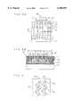
- the first wiring layer 58makes electrical contact with the first electrically conductive layer 53 through the first contact hole 56.
- the second wiring layer 59makes electrical contact with the second electrically conductive layer 55 through the second contact hole 57.
Landscapes
- Physics & Mathematics (AREA)
- Condensed Matter Physics & Semiconductors (AREA)
- General Physics & Mathematics (AREA)
- Engineering & Computer Science (AREA)
- Computer Hardware Design (AREA)
- Microelectronics & Electronic Packaging (AREA)
- Power Engineering (AREA)
- Semiconductor Integrated Circuits (AREA)
- Internal Circuitry In Semiconductor Integrated Circuit Devices (AREA)
Abstract
Description
Claims (24)
Applications Claiming Priority (2)
| Application Number | Priority Date | Filing Date | Title |
|---|---|---|---|
| JP10-142456 | 1998-05-25 | ||
| JP14245698AJP3407020B2 (en) | 1998-05-25 | 1998-05-25 | Semiconductor device |
Publications (1)
| Publication Number | Publication Date |
|---|---|
| US6100591Atrue US6100591A (en) | 2000-08-08 |
Family
ID=15315746
Family Applications (1)
| Application Number | Title | Priority Date | Filing Date |
|---|---|---|---|
| US09/314,582Expired - LifetimeUS6100591A (en) | 1998-05-25 | 1999-05-18 | Semiconductor device and method of fabricating the same |
Country Status (2)
| Country | Link |
|---|---|
| US (1) | US6100591A (en) |
| JP (1) | JP3407020B2 (en) |
Cited By (16)
| Publication number | Priority date | Publication date | Assignee | Title |
|---|---|---|---|---|
| US6353261B1 (en)* | 1999-05-03 | 2002-03-05 | Vlsi Technology, Inc. | Method and apparatus for reducing interconnect resistance using an interconnect well |
| US6445056B2 (en)* | 2000-01-05 | 2002-09-03 | Nec Corporation | Semiconductor capacitor device |
| US6548902B2 (en)* | 2000-12-27 | 2003-04-15 | Fujitsu Limited | Semiconductor integrated circuit device, circuit design apparatus, and circuit design method |
| WO2003090283A3 (en)* | 2002-04-19 | 2004-01-15 | Infineon Technologies Ag | Semiconductor component comprising an integrated capacitor structure that has a plurality of metallization planes |
| US20040089911A1 (en)* | 2002-10-18 | 2004-05-13 | Takeya Fujino | Semiconductor integrated circuit and method of manufacturing the same |
| US20050161706A1 (en)* | 2004-01-26 | 2005-07-28 | Marvell International Ltd. | Interconnect structure for power transistors |
| US20070034904A1 (en)* | 2003-10-22 | 2007-02-15 | Sehat Sutardja | Efficient transistor structure |
| US20070190760A1 (en)* | 2006-01-13 | 2007-08-16 | Coolbaugh Douglas D | Integrated parallel plate capacitors |
| US20070195946A1 (en)* | 2006-02-17 | 2007-08-23 | Fujitsu Limited | Semiconductor integrated circuit device |
| US20080157209A1 (en)* | 2003-10-22 | 2008-07-03 | Sehat Sutardja | Integrated circuits and interconnect structure for integrated circuits |
| US7471225B1 (en) | 2006-02-27 | 2008-12-30 | Marvell International Ltd. | Transmitter digital-to-analog converter with noise shaping |
| US8169081B1 (en) | 2007-12-27 | 2012-05-01 | Volterra Semiconductor Corporation | Conductive routings in integrated circuits using under bump metallization |
| US20160042995A1 (en)* | 2012-04-18 | 2016-02-11 | Micron Technology, Inc. | Interconnect structures for integrated circuits and their formation |
| CN110168707A (en)* | 2017-07-13 | 2019-08-23 | 富士电机株式会社 | Semiconductor device |
| US10504920B2 (en) | 2011-06-01 | 2019-12-10 | Semiconductor Energy Laboratory Co., Ltd. | Semiconductor device |
| US11367695B2 (en)* | 2018-07-31 | 2022-06-21 | Taiwan Semiconductor Manufacturing Company, Ltd. | Interposer with capacitors |
Citations (4)
| Publication number | Priority date | Publication date | Assignee | Title |
|---|---|---|---|---|
| JPS5947755A (en)* | 1982-09-13 | 1984-03-17 | Hitachi Ltd | Semiconductor device |
| JPH0555459A (en)* | 1991-08-28 | 1993-03-05 | Ricoh Co Ltd | Semiconductor integrated circuit device and manufacturing method thereof |
| US5502337A (en)* | 1994-07-04 | 1996-03-26 | Mitsubishi Denki Kabushiki Kaisha | Semiconductor device structure including multiple interconnection layers with interlayer insulating films |
| US5739587A (en)* | 1995-02-21 | 1998-04-14 | Seiko Epson Corporation | Semiconductor device having a multi-latered wiring structure |
- 1998
- 1998-05-25JPJP14245698Apatent/JP3407020B2/ennot_activeExpired - Fee Related
- 1999
- 1999-05-18USUS09/314,582patent/US6100591A/ennot_activeExpired - Lifetime
Patent Citations (4)
| Publication number | Priority date | Publication date | Assignee | Title |
|---|---|---|---|---|
| JPS5947755A (en)* | 1982-09-13 | 1984-03-17 | Hitachi Ltd | Semiconductor device |
| JPH0555459A (en)* | 1991-08-28 | 1993-03-05 | Ricoh Co Ltd | Semiconductor integrated circuit device and manufacturing method thereof |
| US5502337A (en)* | 1994-07-04 | 1996-03-26 | Mitsubishi Denki Kabushiki Kaisha | Semiconductor device structure including multiple interconnection layers with interlayer insulating films |
| US5739587A (en)* | 1995-02-21 | 1998-04-14 | Seiko Epson Corporation | Semiconductor device having a multi-latered wiring structure |
Cited By (47)
| Publication number | Priority date | Publication date | Assignee | Title |
|---|---|---|---|---|
| US6353261B1 (en)* | 1999-05-03 | 2002-03-05 | Vlsi Technology, Inc. | Method and apparatus for reducing interconnect resistance using an interconnect well |
| US6445056B2 (en)* | 2000-01-05 | 2002-09-03 | Nec Corporation | Semiconductor capacitor device |
| US6548902B2 (en)* | 2000-12-27 | 2003-04-15 | Fujitsu Limited | Semiconductor integrated circuit device, circuit design apparatus, and circuit design method |
| US7061746B2 (en) | 2002-04-19 | 2006-06-13 | Infineon Technologies Ag | Semiconductor component with integrated capacitance structure having a plurality of metallization planes |
| WO2003090283A3 (en)* | 2002-04-19 | 2004-01-15 | Infineon Technologies Ag | Semiconductor component comprising an integrated capacitor structure that has a plurality of metallization planes |
| US20050219790A1 (en)* | 2002-04-19 | 2005-10-06 | Hichem Abdallah | Semiconductor component comprising an integrated capacitor structure tha has a plurality of metallization planes |
| US20040089911A1 (en)* | 2002-10-18 | 2004-05-13 | Takeya Fujino | Semiconductor integrated circuit and method of manufacturing the same |
| US6989597B2 (en) | 2002-10-18 | 2006-01-24 | Matsushita Electric Industrial Co., Ltd. | Semiconductor integrated circuit and method of manufacturing the same |
| US20070037353A1 (en)* | 2003-10-22 | 2007-02-15 | Sehat Sutardja | Efficient transistor structure |
| US20080237649A1 (en)* | 2003-10-22 | 2008-10-02 | Sehat Sutardja | Integrated circuits and interconnect structure for integrated circuits |
| US7851872B2 (en) | 2003-10-22 | 2010-12-14 | Marvell World Trade Ltd. | Efficient transistor structure |
| US20070034904A1 (en)* | 2003-10-22 | 2007-02-15 | Sehat Sutardja | Efficient transistor structure |
| US7863657B2 (en) | 2003-10-22 | 2011-01-04 | Marvell World Trade Ltd. | Efficient transistor structure |
| US8026550B2 (en) | 2003-10-22 | 2011-09-27 | Marvell World Trade Ltd. | Integrated circuits and interconnect structure for integrated circuits |
| US7989852B2 (en) | 2003-10-22 | 2011-08-02 | Marvell World Trade Ltd. | Integrated circuits and interconnect structure for integrated circuits |
| US7960833B2 (en) | 2003-10-22 | 2011-06-14 | Marvell World Trade Ltd. | Integrated circuits and interconnect structure for integrated circuits |
| US20080157209A1 (en)* | 2003-10-22 | 2008-07-03 | Sehat Sutardja | Integrated circuits and interconnect structure for integrated circuits |
| US7652338B2 (en) | 2003-10-22 | 2010-01-26 | Marvell World Trade Ltd. | Efficient transistor structure |
| US20080258240A1 (en)* | 2003-10-22 | 2008-10-23 | Sehat Sutardja | Integrated circuits and interconnect structure for integrated circuits |
| US20080258241A1 (en)* | 2003-10-22 | 2008-10-23 | Sehat Sutardja | Integrated circuits and interconnect structure for integrated circuits |
| US7982280B2 (en) | 2003-10-22 | 2011-07-19 | Marvell World Trade Ltd. | Integrated circuits and interconnect structure for integrated circuits |
| US7459381B2 (en)* | 2004-01-26 | 2008-12-02 | Marvell World Trade Ltd. | Integrated circuits and interconnect structure for integrated circuits |
| US20050161706A1 (en)* | 2004-01-26 | 2005-07-28 | Marvell International Ltd. | Interconnect structure for power transistors |
| US20060175709A1 (en)* | 2004-01-26 | 2006-08-10 | Marvell International Ltd. | Integrated circuits and interconnect structure for integrated circuits |
| US7265448B2 (en) | 2004-01-26 | 2007-09-04 | Marvell World Trade Ltd. | Interconnect structure for power transistors |
| EP1727200A3 (en)* | 2004-01-26 | 2006-12-13 | Marvell World Trade Ltd. | Integrated circuits and interconnect structure for integrated circuits |
| US7645675B2 (en)* | 2006-01-13 | 2010-01-12 | International Business Machines Corporation | Integrated parallel plate capacitors |
| US20070190760A1 (en)* | 2006-01-13 | 2007-08-16 | Coolbaugh Douglas D | Integrated parallel plate capacitors |
| US20070195946A1 (en)* | 2006-02-17 | 2007-08-23 | Fujitsu Limited | Semiconductor integrated circuit device |
| US7663175B2 (en)* | 2006-02-17 | 2010-02-16 | Fujitsu Microelectronics Limited | Semiconductor integrated circuit device |
| US7471225B1 (en) | 2006-02-27 | 2008-12-30 | Marvell International Ltd. | Transmitter digital-to-analog converter with noise shaping |
| US7999711B1 (en) | 2006-02-27 | 2011-08-16 | Marvell International Ltd. | Transmitter digital-to-analog converter with noise shaping |
| US8169081B1 (en) | 2007-12-27 | 2012-05-01 | Volterra Semiconductor Corporation | Conductive routings in integrated circuits using under bump metallization |
| US8664767B2 (en) | 2007-12-27 | 2014-03-04 | Volterra Semiconductor Corporation | Conductive routings in integrated circuits using under bump metallization |
| US8933520B1 (en) | 2007-12-27 | 2015-01-13 | Volterra Semiconductor LLC | Conductive routings in integrated circuits using under bump metallization |
| US10504920B2 (en) | 2011-06-01 | 2019-12-10 | Semiconductor Energy Laboratory Co., Ltd. | Semiconductor device |
| US10840137B2 (en) | 2012-04-18 | 2020-11-17 | Micron Technology, Inc. | Methods of forming integrated circuits having parallel conductors |
| US10424506B2 (en) | 2012-04-18 | 2019-09-24 | Micron Technology, Inc. | Integrated circuits having parallel conductors and their formation |
| US9972532B2 (en)* | 2012-04-18 | 2018-05-15 | Micron Technology, Inc. | Interconnect structures for integrated circuits and their formation |
| US10741445B2 (en) | 2012-04-18 | 2020-08-11 | Micron Technology, Inc. | Integrated circuits having parallel conductors |
| US20160042995A1 (en)* | 2012-04-18 | 2016-02-11 | Micron Technology, Inc. | Interconnect structures for integrated circuits and their formation |
| CN110168707A (en)* | 2017-07-13 | 2019-08-23 | 富士电机株式会社 | Semiconductor device |
| US20190326237A1 (en)* | 2017-07-13 | 2019-10-24 | Fuji Electric Co., Ltd. | Semiconductor device |
| US11594502B2 (en)* | 2017-07-13 | 2023-02-28 | Fuji Electric Co., Ltd. | Semiconductor device having conductive film |
| CN110168707B (en)* | 2017-07-13 | 2023-08-29 | 富士电机株式会社 | Semiconductor device with a semiconductor device having a plurality of semiconductor chips |
| US12068268B2 (en) | 2017-07-13 | 2024-08-20 | Fuji Electric Co., Ltd. | Semiconductor device having a wire bonding pad structure connected through vias to lower wiring |
| US11367695B2 (en)* | 2018-07-31 | 2022-06-21 | Taiwan Semiconductor Manufacturing Company, Ltd. | Interposer with capacitors |
Also Published As
| Publication number | Publication date |
|---|---|
| JPH11340418A (en) | 1999-12-10 |
| JP3407020B2 (en) | 2003-05-19 |
Similar Documents
| Publication | Publication Date | Title |
|---|---|---|
| US6100591A (en) | Semiconductor device and method of fabricating the same | |
| US6991980B2 (en) | Methods of manufacturing multi-layer integrated circuit capacitor electrodes | |
| US6500724B1 (en) | Method of making semiconductor device having passive elements including forming capacitor electrode and resistor from same layer of material | |
| US6812109B2 (en) | Integrated decoupling capacitors | |
| JP6639736B2 (en) | Capacitor device and manufacturing method thereof | |
| TW526588B (en) | Semiconductor device and method for manufacturing the same | |
| JP5568494B2 (en) | Integrated circuit capacitor structure | |
| KR100532435B1 (en) | Semiconductor memory device comprising storage nodes and resistors and manufacturing method for the same | |
| TWI292204B (en) | Semiconductor device and method for manufacturing the same | |
| US6411492B1 (en) | Structure and method for fabrication of an improved capacitor | |
| US6656814B2 (en) | Methods of fabricating integrated circuit devices including distributed and isolated dummy conductive regions | |
| JP2002530884A (en) | Improved capacitor with high Q value | |
| US6150254A (en) | Method for wiring of a semiconductor device | |
| JP2001223340A (en) | Capacitor and method of forming the same | |
| US20080090376A1 (en) | Method of fabricating semiconductor device | |
| JP3109478B2 (en) | Semiconductor device | |
| JP3987703B2 (en) | Capacitor element and manufacturing method thereof | |
| CN100479162C (en) | Semiconductor element and its manufacturing method | |
| JP4342226B2 (en) | Semiconductor device and manufacturing method thereof | |
| US7745300B2 (en) | Method for forming a capacitor in a semiconductor and a capacitor using the same | |
| JP2005005647A (en) | Semiconductor device and manufacturing method thereof | |
| US20090166805A1 (en) | Metal Insulator Metal Capacitor and Method of Manufacturing the Same | |
| KR100571401B1 (en) | Capacitor Formation Method for Semiconductor Device | |
| KR100591174B1 (en) | Metal-insulator-metal capacitors for semiconductor devices and methods of manufacturing the same | |
| JPS611048A (en) | Memory element |
Legal Events
| Date | Code | Title | Description |
|---|---|---|---|
| AS | Assignment | Owner name:NEC CORPORATION, JAPAN Free format text:ASSIGNMENT OF ASSIGNORS INTEREST;ASSIGNOR:ISHII, KOJI;REEL/FRAME:009986/0681 Effective date:19990510 | |
| STCF | Information on status: patent grant | Free format text:PATENTED CASE | |
| FEPP | Fee payment procedure | Free format text:PAYOR NUMBER ASSIGNED (ORIGINAL EVENT CODE: ASPN); ENTITY STATUS OF PATENT OWNER: LARGE ENTITY | |
| AS | Assignment | Owner name:NEC ELECTRONICS CORPORATION, JAPAN Free format text:ASSIGNMENT OF ASSIGNORS INTEREST;ASSIGNOR:NEC CORPORATION;REEL/FRAME:013751/0721 Effective date:20021101 | |
| FPAY | Fee payment | Year of fee payment:4 | |
| FPAY | Fee payment | Year of fee payment:8 | |
| AS | Assignment | Owner name:RENESAS ELECTRONICS CORPORATION, JAPAN Free format text:CHANGE OF NAME;ASSIGNOR:NEC ELECTRONICS CORPORATION;REEL/FRAME:025185/0906 Effective date:20100401 | |
| FPAY | Fee payment | Year of fee payment:12 | |
| AS | Assignment | Owner name:STARBOARD VALUE INTERMEDIATE FUND LP, AS COLLATERAL AGENT, NEW YORK Free format text:PATENT SECURITY AGREEMENT;ASSIGNORS:ACACIA RESEARCH GROUP LLC;AMERICAN VEHICULAR SCIENCES LLC;BONUTTI SKELETAL INNOVATIONS LLC;AND OTHERS;REEL/FRAME:052853/0153 Effective date:20200604 | |
| AS | Assignment | Owner name:BONUTTI SKELETAL INNOVATIONS LLC, TEXAS Free format text:RELEASE OF SECURITY INTEREST IN PATENTS;ASSIGNOR:STARBOARD VALUE INTERMEDIATE FUND LP;REEL/FRAME:053654/0254 Effective date:20200630 Owner name:MOBILE ENHANCEMENT SOLUTIONS LLC, TEXAS Free format text:RELEASE OF SECURITY INTEREST IN PATENTS;ASSIGNOR:STARBOARD VALUE INTERMEDIATE FUND LP;REEL/FRAME:053654/0254 Effective date:20200630 Owner name:SUPER INTERCONNECT TECHNOLOGIES LLC, TEXAS Free format text:RELEASE OF SECURITY INTEREST IN PATENTS;ASSIGNOR:STARBOARD VALUE INTERMEDIATE FUND LP;REEL/FRAME:053654/0254 Effective date:20200630 Owner name:STINGRAY IP SOLUTIONS LLC, TEXAS Free format text:RELEASE OF SECURITY INTEREST IN PATENTS;ASSIGNOR:STARBOARD VALUE INTERMEDIATE FUND LP;REEL/FRAME:053654/0254 Effective date:20200630 Owner name:LIFEPORT SCIENCES LLC, TEXAS Free format text:RELEASE OF SECURITY INTEREST IN PATENTS;ASSIGNOR:STARBOARD VALUE INTERMEDIATE FUND LP;REEL/FRAME:053654/0254 Effective date:20200630 Owner name:INNOVATIVE DISPLAY TECHNOLOGIES LLC, TEXAS Free format text:RELEASE OF SECURITY INTEREST IN PATENTS;ASSIGNOR:STARBOARD VALUE INTERMEDIATE FUND LP;REEL/FRAME:053654/0254 Effective date:20200630 Owner name:MONARCH NETWORKING SOLUTIONS LLC, CALIFORNIA Free format text:RELEASE OF SECURITY INTEREST IN PATENTS;ASSIGNOR:STARBOARD VALUE INTERMEDIATE FUND LP;REEL/FRAME:053654/0254 Effective date:20200630 Owner name:PARTHENON UNIFIED MEMORY ARCHITECTURE LLC, TEXAS Free format text:RELEASE OF SECURITY INTEREST IN PATENTS;ASSIGNOR:STARBOARD VALUE INTERMEDIATE FUND LP;REEL/FRAME:053654/0254 Effective date:20200630 Owner name:AMERICAN VEHICULAR SCIENCES LLC, TEXAS Free format text:RELEASE OF SECURITY INTEREST IN PATENTS;ASSIGNOR:STARBOARD VALUE INTERMEDIATE FUND LP;REEL/FRAME:053654/0254 Effective date:20200630 Owner name:LIMESTONE MEMORY SYSTEMS LLC, CALIFORNIA Free format text:RELEASE OF SECURITY INTEREST IN PATENTS;ASSIGNOR:STARBOARD VALUE INTERMEDIATE FUND LP;REEL/FRAME:053654/0254 Effective date:20200630 Owner name:ACACIA RESEARCH GROUP LLC, NEW YORK Free format text:RELEASE OF SECURITY INTEREST IN PATENTS;ASSIGNOR:STARBOARD VALUE INTERMEDIATE FUND LP;REEL/FRAME:053654/0254 Effective date:20200630 Owner name:UNIFICATION TECHNOLOGIES LLC, TEXAS Free format text:RELEASE OF SECURITY INTEREST IN PATENTS;ASSIGNOR:STARBOARD VALUE INTERMEDIATE FUND LP;REEL/FRAME:053654/0254 Effective date:20200630 Owner name:NEXUS DISPLAY TECHNOLOGIES LLC, TEXAS Free format text:RELEASE OF SECURITY INTEREST IN PATENTS;ASSIGNOR:STARBOARD VALUE INTERMEDIATE FUND LP;REEL/FRAME:053654/0254 Effective date:20200630 Owner name:R2 SOLUTIONS LLC, TEXAS Free format text:RELEASE OF SECURITY INTEREST IN PATENTS;ASSIGNOR:STARBOARD VALUE INTERMEDIATE FUND LP;REEL/FRAME:053654/0254 Effective date:20200630 Owner name:CELLULAR COMMUNICATIONS EQUIPMENT LLC, TEXAS Free format text:RELEASE OF SECURITY INTEREST IN PATENTS;ASSIGNOR:STARBOARD VALUE INTERMEDIATE FUND LP;REEL/FRAME:053654/0254 Effective date:20200630 Owner name:SAINT LAWRENCE COMMUNICATIONS LLC, TEXAS Free format text:RELEASE OF SECURITY INTEREST IN PATENTS;ASSIGNOR:STARBOARD VALUE INTERMEDIATE FUND LP;REEL/FRAME:053654/0254 Effective date:20200630 Owner name:TELECONFERENCE SYSTEMS LLC, TEXAS Free format text:RELEASE OF SECURITY INTEREST IN PATENTS;ASSIGNOR:STARBOARD VALUE INTERMEDIATE FUND LP;REEL/FRAME:053654/0254 Effective date:20200630 | |
| AS | Assignment | Owner name:STARBOARD VALUE INTERMEDIATE FUND LP, AS COLLATERAL AGENT, NEW YORK Free format text:CORRECTIVE ASSIGNMENT TO CORRECT THE ASSIGNOR NAME PREVIOUSLY RECORDED ON REEL 052853 FRAME 0153. ASSIGNOR(S) HEREBY CONFIRMS THE PATENT SECURITY AGREEMENT;ASSIGNOR:ACACIA RESEARCH GROUP LLC;REEL/FRAME:056775/0066 Effective date:20200604 | |
| AS | Assignment | Owner name:ACACIA RESEARCH GROUP LLC, NEW YORK Free format text:CORRECTIVE ASSIGNMENT TO CORRECT THE ASSIGNEE NAME PREVIOUSLY RECORDED AT REEL: 053654 FRAME: 0254. ASSIGNOR(S) HEREBY CONFIRMS THE ASSIGNMENT;ASSIGNOR:STARBOARD VALUE INTERMEDIATE FUND LP;REEL/FRAME:057454/0045 Effective date:20200630 |