US6100195A - Passivation of copper interconnect surfaces with a passivating metal layer - Google Patents
Passivation of copper interconnect surfaces with a passivating metal layerDownload PDFInfo
- Publication number
- US6100195A US6100195AUS09/222,275US22227598AUS6100195AUS 6100195 AUS6100195 AUS 6100195AUS 22227598 AUS22227598 AUS 22227598AUS 6100195 AUS6100195 AUS 6100195A
- Authority
- US
- United States
- Prior art keywords
- layer
- copper
- trench hole
- alloy
- interconnect trench
- Prior art date
- Legal status (The legal status is an assumption and is not a legal conclusion. Google has not performed a legal analysis and makes no representation as to the accuracy of the status listed.)
- Expired - Lifetime
Links
Images


Classifications
- H—ELECTRICITY
- H01—ELECTRIC ELEMENTS
- H01L—SEMICONDUCTOR DEVICES NOT COVERED BY CLASS H10
- H01L21/00—Processes or apparatus adapted for the manufacture or treatment of semiconductor or solid state devices or of parts thereof
- H01L21/70—Manufacture or treatment of devices consisting of a plurality of solid state components formed in or on a common substrate or of parts thereof; Manufacture of integrated circuit devices or of parts thereof
- H01L21/71—Manufacture of specific parts of devices defined in group H01L21/70
- H01L21/768—Applying interconnections to be used for carrying current between separate components within a device comprising conductors and dielectrics
- H01L21/76838—Applying interconnections to be used for carrying current between separate components within a device comprising conductors and dielectrics characterised by the formation and the after-treatment of the conductors
- H01L21/76841—Barrier, adhesion or liner layers
- H01L21/76843—Barrier, adhesion or liner layers formed in openings in a dielectric
- H01L21/76849—Barrier, adhesion or liner layers formed in openings in a dielectric the layer being positioned on top of the main fill metal
- H—ELECTRICITY
- H01—ELECTRIC ELEMENTS
- H01L—SEMICONDUCTOR DEVICES NOT COVERED BY CLASS H10
- H01L21/00—Processes or apparatus adapted for the manufacture or treatment of semiconductor or solid state devices or of parts thereof
- H01L21/70—Manufacture or treatment of devices consisting of a plurality of solid state components formed in or on a common substrate or of parts thereof; Manufacture of integrated circuit devices or of parts thereof
- H01L21/71—Manufacture of specific parts of devices defined in group H01L21/70
- H01L21/768—Applying interconnections to be used for carrying current between separate components within a device comprising conductors and dielectrics
- H01L21/76838—Applying interconnections to be used for carrying current between separate components within a device comprising conductors and dielectrics characterised by the formation and the after-treatment of the conductors
- H01L21/76841—Barrier, adhesion or liner layers
- H01L21/76853—Barrier, adhesion or liner layers characterized by particular after-treatment steps
- H01L21/76855—After-treatment introducing at least one additional element into the layer
- H01L21/76858—After-treatment introducing at least one additional element into the layer by diffusing alloying elements
- H—ELECTRICITY
- H01—ELECTRIC ELEMENTS
- H01L—SEMICONDUCTOR DEVICES NOT COVERED BY CLASS H10
- H01L21/00—Processes or apparatus adapted for the manufacture or treatment of semiconductor or solid state devices or of parts thereof
- H01L21/70—Manufacture or treatment of devices consisting of a plurality of solid state components formed in or on a common substrate or of parts thereof; Manufacture of integrated circuit devices or of parts thereof
- H01L21/71—Manufacture of specific parts of devices defined in group H01L21/70
- H01L21/768—Applying interconnections to be used for carrying current between separate components within a device comprising conductors and dielectrics
- H01L21/76838—Applying interconnections to be used for carrying current between separate components within a device comprising conductors and dielectrics characterised by the formation and the after-treatment of the conductors
- H01L21/76841—Barrier, adhesion or liner layers
- H01L21/76867—Barrier, adhesion or liner layers characterized by methods of formation other than PVD, CVD or deposition from a liquids
- H—ELECTRICITY
- H01—ELECTRIC ELEMENTS
- H01L—SEMICONDUCTOR DEVICES NOT COVERED BY CLASS H10
- H01L21/00—Processes or apparatus adapted for the manufacture or treatment of semiconductor or solid state devices or of parts thereof
- H01L21/70—Manufacture or treatment of devices consisting of a plurality of solid state components formed in or on a common substrate or of parts thereof; Manufacture of integrated circuit devices or of parts thereof
- H01L21/71—Manufacture of specific parts of devices defined in group H01L21/70
- H01L21/768—Applying interconnections to be used for carrying current between separate components within a device comprising conductors and dielectrics
- H01L21/76838—Applying interconnections to be used for carrying current between separate components within a device comprising conductors and dielectrics characterised by the formation and the after-treatment of the conductors
- H01L21/76886—Modifying permanently or temporarily the pattern or the conductivity of conductive members, e.g. formation of alloys, reduction of contact resistances
Definitions
- This inventionrelates to interconnects formed in semiconductor devices, and more particularly to copper interconnects formed in Inter-Metallic Dielectric (IMD) layers.
- IMDInter-Metallic Dielectric
- U.S. Pat. No. 5,674,787 of Zhao et al. for "Selective Electroless Copper Deposited Interconnect Plugs for ULSI Applications”shows selective Cu electroless deposition in a via trench hole using a seed layer.
- An electroless copper deposition methodselectively forms encapsulated copper plugs to connect conductive regions of a semiconductor device.
- a contact displacement techniqueforms a thin activation copper layer on a barrier metal layer, e.g. TiN, which is present as a covering layer on an underlying metal layer. Copper is deposited in the via by an electroless auto-catalytic process.
- Electroless copper depositioncontinues until the via is almost filled which leaves sufficient room at the top for an upper encapsulation to be formed there, but first the device is rinsed in DI (deionized) water to remove the electroless deposition solution. Then after the rising away of the electroless copper solution, a cap barrier layer, from 500 ⁇ to about 1500 ⁇ thick, is formed of a variety of metals or metal alloys such as Ni, Co, Ni--Co alloy, CoP, NiCoP, or NiP from another electroless solution. The bottom barrier layer and the cap barrier layer complete the full encapsulation of the copper plug via.
- DIdeionized
- An interconnect line on an IMD layer on a semiconductor deviceis formed in an interconnect hole in the IMD layer.
- the interconnect holehas walls and a bottom in the IMD layer.
- a diffusion barrieris formed on the walls and the bottom of the hole.
- a passivating metal layeris deposited selectively on the surface of the copper metal deposit encapsulating the copper metal plug.
- a blanket deposit of a copper metal layercovers the diffusion layer and fills the interconnect hole with a copper metal deposit.
- Perform a CMP processto planarize the device to remove both copper and the barrier metal at the IMD layer.
- FIGS. 1A-1Gillustrate a problem which led to development of this invention, showing fragmentary sectional views of a device during a manufacturing process.
- FIGS. 2A-2Killustrate a solution in accordance with this invention to the problem of FIGS. 1A-1G.
- FIGS. 2A-2Kshow fragmentary sectional views of the process of manufacturing a portion of a semiconductor device.
- FIGS. 3A-3Dwhich illustrate a solution to the problem described above, show fragmentary sectional views a device during manufacture of a portion of a semiconductor device in accordance with this invention.
- FIGS. 4A-4Cshow fragmentary sectional views of a device during manufacture of a portion of a semiconductor device with a process modified from FIGS. 1A-1G.
- FIGS. 5A-5Cshow fragmentary sectional views of a device during a process of manufacture of a portion of a semiconductor device with a process modified from FIGS. 1A-1G.
- copperWith the reduction in device dimensions to deep submicron regimes such as a sub 0.25 ⁇ m regime, we believe that copper emerges as the leading candidate to replace aluminum as the interconnect metal of choice because of its lower resistivity and longer electromigration lifetime.
- One of the most serious drawbacks of copper metallizationis the instability of copper in an oxidizing ambient which leads to formation of copper oxide which degrades the electrical performance of the device and causes the issue of reduction in reliability of the devices.
- Copperis unlike aluminum, which is a self-passivating or self-healing metal which forms a protective layer of aluminum oxide. To the contrary, copper oxide continues to oxidize the remaining copper in the structure, eventually consuming most or all of the copper, especially in the thin films of copper employed in thin film devices, such as the semiconductor devices of this invention. Thus, we have found that copper needs to be passivated for protection from oxidation prior to thermal treatment of the semiconductor device.
- FIGS. 1A-1Gillustrate a problem which led to development of this invention, showing fragmentary sectional views of semiconductor device 10 during a process of manufacturing a portion thereof. This process, as described below, was considered for use and the problems found therewith have led to the development this invention, but found to be lacking as will be explained at the end of the description thereof.
- FIG. 1Ashows a fragmentary sectional view of a portion of a semiconductor device 10 in early stage of the process of manufacturing in accordance with the steps shown in FIGS. 1A-1E.
- An Inter-Metallic Dielectric (IMD) layer 12composed of a material such as an oxide of silicon formed by a silane (SiH 4 ) or TEOS process or a Spin on Polymer (SOP), which is formed on the device 10 has a filled trench hole 13 that has been coated with a thin layer of a metal nitride, diffusion barrier layer 14 composed of a refractory metal nitride selected from the group consisting of titanium nitride (TiN), tantalum nitride (TaN) and tungsten nitride (WN). Then a lower interconnect copper line 16 has been formed to fill the remaining space in the trench hole 13. Lower interconnect copper line 16 is bonded to the metal nitride, diffusion barrier layer 14.
- IMDInter-Metallic Dielectric
- SiN
- FIG. 1Bshows the device 10 of FIG. 1A after the following step of CMP (Chemical Mechanical Polishing) of the copper line 16 to planarize the surface of the device 10 by removing that portion of the copper line 16 and of the diffusion barrier metal nitride 14 which extends above the surface of the IMD layer 12.
- CMPChemical Mechanical Polishing
- FIG. 1Cshows the device 10 of FIG. 1B after a blanket silicon nitride (Si 3 N 4 ) dielectric layer 18 has been deposited upon the surface of device 10 covering the top surface of the planarized lower interconnect copper line 16, the exposed portion of the surface of the IMD layer 12 and the edges of the diffusion barrier metal layer 14 on the top of device 10 between the IMD layer 12 and the copper line 16.
- Si 3 N 4silicon nitride
- FIG. 1Dshows the device 10 of FIG. 1C after a blanket silicon oxide layer 20 such as an Inter-Metallic Dielectric (IMD) layer composed of a material such as an oxide of silicon has been formed on top of silicon nitride layer 18.
- Silicon nitride layer 18has been formed by a TEOS process or a Spin-on-Glass (SOG).
- FIG. 1Eshows the device 10 of FIG. 1D after the silicon oxide layer 20 has been patterned (using photolithographic and etching processes well known to those skilled in the art) to form a hard mask of layer 20 with a trench hole 21 etched therethrough. Etching through hole 21 continues until the trench hole 21 is etched further down through silicon nitride layer 18 to the surface of lower interconnect copper line 16. Thus, the contact trench hole 21 has been etched down through silicon oxide layer 20 and silicon nitride layer 18 to expose a substantial portion of the surface of lower copper interconnect line 16.
- FIG. 1Fshows the device 10 of FIG. 1E after the trench hole 21 has been widened on the margins slightly above silicon nitride layer 18 to make a larger trench hole 21 (now filled).
- Thin film, metal nitride, barrier layer 22was formed lining the trench hole 21 and the top surface of silicon oxide layer 20 was coated with thin film barrier layer 22.
- Thin film, metal nitride, diffusion barrier layer 22composed of an electrically conductive, refractory metal nitride selected from the group consisting of titanium nitride (TiN), tantalum nitride (TaN) and tungsten nitride (WN) covering the exposed surface portion of lower copper interconnect line 16, on the exposed surfaces of silicon nitride layer 18 in trench hole 21, and on the exposed surfaces of upper IMD layer 20.
- an upper copper interconnect line 24is formed in the space remaining in the trench hole 21 bonded to the upper diffusion barrier layer 22 and in electrical connection through upper diffusion barrier metal nitride layer 22 to the lower interconnect copper line 16.
- FIG. 1Gshows the device 10 of FIG. 1F after a second copper CMP (Chemical Mechanical Polishing) of the copper interconnect line 24 to planarize the surface of the device 10 by removing that portion of the copper line 24 and of the upper diffusion barrier metal nitride 22 which extends above the surface of the IMD layer 12.
- CMPChemical Mechanical Polishing
- FIGS. 1A-1Gwhich has been considered for use involves a copper CMP (Chemical Mechanical Polishing) step and deposition of a silicon nitride (Si 3 N 4 ) capping layer 18.
- a copper CMPChemical Mechanical Polishing
- a silicon nitrideSi 3 N 4
- This approachmay result in higher RC (Resistance Capacitance) delay and formation of copper halides and copper oxides.
- the RC delayis caused by the higher dielectric constant of silicon nitride.
- FIGS. 2A-2Killustrate a solution in accordance with this invention to the problem described above, showing fragmentary sectional views of a semiconductor device 50 during a process of manufacture thereof.
- FIG. 2Ashows a fragmentary sectional view of a portion of a semiconductor device 50 in early stage of the process of manufacturing in accordance with the steps shown in FIGS. 2A-2K comprising a lower Inter-Metallic Dielectric (IMD) layer 52 composed of a material such as an oxide of silicon, such as Spin on Glass (SOG) in which is formed an interconnect trench hole 53 which is preferably deeper in the center CE and has ledges 51 on either side of center CE.
- the ledges 51are shallower than the center CE.
- FIG. 2Bshows the device 50 of FIG. 2A after forming a diffusion barrier layer 54 on the IMD layer 52 including the top surface of layer 52 as well as covering the walls, ledges and the bottom of the trench hole 53 in layer 52.
- the thin layer of diffusion barrier layer 54are composed of a refractory metal nitride is preferably composed of a material selected from the group consisting of titanium nitride (TiN), tantalum nitride (TaN) and tungsten nitride (WN).
- FIG. 2Cshows the device 50 of FIG. 2B after a lower interconnect copper line 56 has been formed filling the space 53' remaining in the trench hole 53 (after depositing layer 54) and copper line has been deposited to cover the device 50 to a level well above the uppermost surface of layer 54.
- the copper line 56is bonded to the diffusion barrier layer 54.
- FIG. 2Dshows the device 50 of FIG. 2C after the top surface of copper line 56 and diffusion layer 54 have been planarized by CMP (Chemical Mechanical Polishing) step to be level with the IMD layer 52.
- CMPChemical Mechanical Polishing
- FIG. 2Eshows the device 50 of FIG. 2D after a blanket aluminum (Al), platinum (Pt) or palladium (Pd) passivation layer 59 has been formed on the surface of device 50 with a thickness from about 50 ⁇ to about 300 ⁇ forms a bilayer of copper 56 and aluminum (Al), platinum (Pt) or palladium (Pd) 59.
- Layer 59overlies the copper line 56 and the exposed surfaces of the IMD layer 52.
- FIG. 2Fshows device 50 of FIG. 2E after annealing of device 50 at a temperature from about 200° C. to about 400° C. forming an alloy 61 of copper-aluminum (Cu--Al), copper-platinum (Pt) (Cu--Pt) or copper-palladium (Pd) (Cu--Pd) alloy at the interface between copper layer 56 and passivation layer 59.
- Cu-Alcopper-aluminum
- Ptcopper-platinum
- Pdcopper-palladium
- FIG. 2Gshows the device 50 of FIG. 2F after etching the device in an acid etchant solution selective to remove aluminum (Al), platinum (Pt) or palladium (Pd) from the surface of device 50, leaving the copper-aluminum (Al), platinum (Pt) or palladium (Pd) alloy 61 in place.
- FIG. 2Hshows the device 50 of FIG. 2F after formation of a blanket Inter-Metallic Dielectric (IMD) layer 64 composed of a material such as an oxide of silicon, such as Spin on Polymer (SOP) over the alloy layer 61, the edge of diffusion barrier layer 54, and the lower IMD layer 52.
- IMDInter-Metallic Dielectric
- FIG. 2Ishows the device 50 of FIG. 2H after patterning using conventional masking and etching techniques to form of an interconnect trench hole 65 which is preferably deeper in the center CE' and has ledges 63 on either side of the center CE'. Ledges 63 are shallower than the center CE'.
- FIG. 2Jshows the device 50 of FIG. 2I after formation of a diffusion barrier layer 66 covering the top surface of IMD layer 64 as well as the walls, ledges and the bottom of the trench hole 65 in IMD layer 64.
- the thin layer of a diffusion barrier layer 66is preferably composed of a refractory metal nitride selected from the group consisting of titanium nitride (TiN), tantalum nitride (TaN) and tungsten nitride (WN).
- FIG. 2Kshows the device 50 of FIG. 2J after an upper interconnect copper line 68 has been formed filling space 65' remaining in the trench hole 65 (after depositing layer 66).
- Upper interconnect copper line 68is bonded to diffusion barrier layer 66. Then the top surface of upper interconnect copper line 68 is planarized by CMP (Chemical Mechanical Polishing) step to be level with IMD layer 54.
- CMPChemical Mechanical Polishing
- the exposed surface of the copper layer of a device in accordance with this inventioncan be selectively covered with an electroless metal barrier, e.g. Pd from about 50 ⁇ to about 300 ⁇ thick, it will eliminate the step of patterning the passivation layer in a self-aligned encapsulation.
- an electroless metal barriere.g. Pd from about 50 ⁇ to about 300 ⁇ thick
- Another advantage of this processis elimination of the removal/etching of the extra passivating material on the non-copper surfaces of the device, such as TEOS. It can also serve as adhesion and diffusion barrier.
- electroless depositionhas the advantage of low cost and low processing temperatures.
- FIGS. 3A-3Dwhich illustrate a solution to the problem described above, show fragmentary sectional views a process of manufacture of a portion of a semiconductor device 80.
- FIG. 3Ashows a fragmentary sectional view of a portion of a semiconductor device 80 in early stage of the process of manufacturing in accordance with the steps shown in FIGS. 3A-3D comprising a lower Inter-Metallic Dielectric (IMD) layer 82 composed of a material such as an oxide of silicon, such as Spin on Polymer (SOP) in which is formed an interconnect trench hole 83' shown after formation of thin film, metal nitride, diffusion barrier layer 84 therein on device 80.
- IMDInter-Metallic Dielectric
- SOPSpin on Polymer
- Thin film, metal nitride, diffusion barrier layer 84covers the IMD layer 82 including the top surface of layer 82 as well as covering the walls, ledges and the bottom of the trench hole 83' in layer 82.
- the thin film, metal nitride, diffusion barrier layer 84is composed of a refractory metal nitride which is preferably composed of a material selected from the group consisting of titanium nitride (TiN), tantalum nitride (TaN) and tungsten nitride (WN).
- FIG. 3Bshows the device 80 of FIG. 3A after a blanket deposition of copper on device 80 to form the lower interconnect copper line 86, covering layer 84 and filling the space in the trench hole 83' inside the diffusion barrier layer 84.
- the copper line 86is bonded to the diffusion barrier layer 84.
- the copperis deposited by a process of copper deposition selected from Chemical Vapor Deposition (CVD), IMP, or plating by an electroless or electroplating process.
- FIG. 3Cshows the device 80 of FIG. 3B after the top surface of copper line 86 has been planarized by CMP (Chemical Mechanical Polishing) step to be level with the IMD layer 82.
- CMPChemical Mechanical Polishing
- FIG. 3Dshows device 80 of FIG. 3C after electroless plating of a metal barrier layer 91 of aluminum (Al), platinum (Pt) or palladium (Pd) has been formed on top of the copper line 86 with a thickness from about 50 ⁇ to about 300 ⁇ thick.
- a metal barrier layer 91 of aluminum (Al), platinum (Pt) or palladium (Pd)has been formed on top of the copper line 86 with a thickness from about 50 ⁇ to about 300 ⁇ thick.
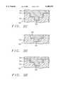
- FIGS. 4A-4Cwhich illustrate a problem which led to development of the second embodiment of this invention.
- FIGS. 4A-4Cshow fragmentary sectional views of a process of manufacture of a portion of a semiconductor device 10A. This process, as described below, was considered before this invention, but found to be lacking as will be explained at the end of the description thereof.
- FIG. 4Ashows a fragmentary sectional view of a portion of a semiconductor device 10A in an early stage of the process of manufacturing in accordance with the steps shown in FIGS. 4A-4C.
- An Inter-Metallic Dielectric (IMD) layer 12Acomposed of a material, such as an oxide of silicon, such as Spin on Polymer (SOP), which is formed on the device 10A has a filled trench hole 11A that has been coated with a thin film, metal nitride diffusion barrier layer 14A.
- Barrier layer 14Ais composed of a refractory metal nitride selected from the group consisting of titanium nitride (TiN), tantalum nitride (TaN) and tungsten nitride (WN).
- a lower interconnect copper line 16Ahas been formed to fill the remaining space in the trench hole 11A.
- Lower interconnect copper line 16Ais bonded to the diffusion barrier layer 14A.
- the followed stepis CMP (Chemical Mechanical Polishing) of the copper line 16A to planarize the surface of the device 10A by removing that copper and the diffusion barrier layer 14A where it extends above the surface of IMD layer 12A.
- FIG. 4Bshows the device 10A of FIG. 4A after a blanket silicon nitride (Si 3 N 4 ) dielectric layer 18A deposited by PECVD (Plasma Enhanced Chemical Vapor Deposition) with a thickness of about 200 ⁇ has been deposited upon the surface of device 10A covering the top surface of the planarized lower interconnect copper line 16A and the exposed portions of the surface of IMD layer 12A and layer 14A on the top of device 10A.
- PECVDPullasma Enhanced Chemical Vapor Deposition
- FIG. 4Cshows the device 10A of FIG. 4B after a blanket silicon oxide layer 20A such as an Inter-Metallic Dielectric (IMD) layer composed of a material such as an oxide of silicon has been formed on top of silicon nitride layer 18A.
- IMDInter-Metallic Dielectric
- the silicon oxide layer 20Ahas been patterned into a hard mask with a trench hole 21A etched therethrough. Etching continues until the trench hole 21A is etched further down through silicon nitride layer 18A to the surface of lower interconnect copper line 16A. Thus, the contact trench hole 21A has been etched down through silicon oxide layer 20A and silicon nitride layer 18A to expose a substantial portion of the surface of lower copper interconnect line 16A.
- the trench hole 21Ahas been widened on the margins slightly above diffusion barrier layer 14A.
- the silicon nitride layer 18A on top of the copper line 16Awill cause an RC delay. Overetching of the silicon nitride layer 18A will harm the first copper metal layer 16A with a chance of contamination by increasing the presence of copper halides which are non-volatile.
- Silicon nitride layer 18Ais used as a passivation layer for trench hole 21A (now filled). Then the top surface of device 10A was coated with upper diffusion barrier layer 22A with the result that the trench hole 21A was lined with barrier layer 22A and at the same time the top surface of silicon oxide layer 20A was coated with barrier layer 22A.
- Barrier layer 22Acomprises a thin layer composed of a refractory metal nitride selected from the group consisting of titanium nitride (TiN), tantalum nitride (TaN) and tungsten nitride (WN) covering the exposed surface portion of lower copper interconnect line 16A, on the exposed surfaces of silicon nitride layer 18A in trench hole 21A, and on the exposed surfaces of upper IMD layer 20A. Then an upper copper interconnect line 24A is formed in the space remaining in the trench hole 21A bonded to the upper diffusion barrier layer 22A and in electrical connection through upper diffusion barrier layer 22A to the lower interconnect copper line 16A followed by a second copper CMP (Chemical Mechanical Polishing) step to be level with IMD layer 20A.
- a refractory metal nitrideselected from the group consisting of titanium nitride (TiN), tantalum nitride (TaN) and tungsten nitride (WN) covering the exposed surface portion
- device 10Ais coated with blanket silicon nitride (Si 3 N 4 ) dielectric layer 28A deposited by PECVD (Plasma Enhanced CVD) with a thickness of about 200 ⁇ has been deposited upon the surface of device 10A covering the top surface of the planarized lower interconnect copper line 24A, the edge of barrier layer 22A and the exposed portions of the surface of IMD layer 20A on the top of device 10A.
- PECVDPullasma Enhanced CVD
- a disadvantage of the process of FIGS. 4A to 4Cis that the silicon nitride on the non-copper layer has to be etched back for the following connection through layer 18A in FIG. 4C forming the following the refractory metal nitride as upper diffusion barrier layer 22A.
- FIGS. 5A-5Cwhich illustrate a problem which led to development of the second embodiment of this invention.
- FIGS. 5A-5Cshow fragmentary sectional views of a process of manufacture of a portion of a semiconductor device 10B. This process, as described below, was considered before this invention, but found to be lacking as will be explained at the end of the description thereof.
- FIG. 5Ashows a fragmentary sectional view of a portion of a semiconductor device 10B in early stage of the process of manufacturing in accordance with the steps shown in FIGS. 5A-5C.
- An Inter-Metallic Dielectric (IMD) layer 12Bcomposed of a material such as an oxide of silicon, such as Spin on Polymer (SOP), which is formed on the device 10B has a trench hole 11B that has been coated with a thin layer of a diffusion barrier layer 14B composed of a refractory metal nitride selected from the group consisting of titanium nitride (TiN), tantalum nitride (TaN) and tungsten nitride (WN).
- TiNtitanium nitride
- TaNtantalum nitride
- WNtungsten nitride
- a lower interconnect copper line 16Ahas been formed to fill the remaining space in the trench hole 11B.
- Lower interconnect copper line 16Ais bonded to the diffusion barrier layer 14B.
- the followed stepis CMP (Chemical Mechanical Polishing) of the copper line 16B to planarize the surface of the device 10B by removing that copper and the diffusion barrier layer 14B where it extends above the surface of IMD layer 12B.
- FIG. 5Bshows the device 10B of FIG. 5A after a blanket titanium or tantalum refractory metal layer 17 deposited to a thickness of about 300 ⁇ has been deposited upon the surface of device 10B covering the top surface of the planarized lower interconnect copper line 16B and the exposed portions of the surface of IMD layer 12B and layer 14B on the top of device 10B.
- FIG. 5Cshows the device 10B of FIG. 5B after patterning of the titanium or tantalum refractory metal layer 17 by conventional photolithography and etching techniques to be aligned with the edges of the hole 11B into which layers 14B and 16B.
- a disadvantage of the process of FIGS. 5A to 5Cis that extra masking is required to pattern the refractory metal layer 17. Another disadvantage is that there is no self-alignment. Furthermore, there is the problem that an extra etching step is required.
Landscapes
- Engineering & Computer Science (AREA)
- Physics & Mathematics (AREA)
- Condensed Matter Physics & Semiconductors (AREA)
- General Physics & Mathematics (AREA)
- Manufacturing & Machinery (AREA)
- Computer Hardware Design (AREA)
- Microelectronics & Electronic Packaging (AREA)
- Power Engineering (AREA)
- Internal Circuitry In Semiconductor Integrated Circuit Devices (AREA)
Abstract
Description
Claims (18)
Priority Applications (3)
| Application Number | Priority Date | Filing Date | Title |
|---|---|---|---|
| US09/222,275US6100195A (en) | 1998-12-28 | 1998-12-28 | Passivation of copper interconnect surfaces with a passivating metal layer |
| SG9901598ASG102536A1 (en) | 1998-12-28 | 1999-03-31 | Passivation of copper interconnect surfaces with a passivating metal layer |
| US09/617,009US6468906B1 (en) | 1998-12-28 | 2000-07-14 | Passivation of copper interconnect surfaces with a passivating metal layer |
Applications Claiming Priority (1)
| Application Number | Priority Date | Filing Date | Title |
|---|---|---|---|
| US09/222,275US6100195A (en) | 1998-12-28 | 1998-12-28 | Passivation of copper interconnect surfaces with a passivating metal layer |
Related Child Applications (1)
| Application Number | Title | Priority Date | Filing Date |
|---|---|---|---|
| US09/617,009DivisionUS6468906B1 (en) | 1998-12-28 | 2000-07-14 | Passivation of copper interconnect surfaces with a passivating metal layer |
Publications (1)
| Publication Number | Publication Date |
|---|---|
| US6100195Atrue US6100195A (en) | 2000-08-08 |
Family
ID=22831587
Family Applications (2)
| Application Number | Title | Priority Date | Filing Date |
|---|---|---|---|
| US09/222,275Expired - LifetimeUS6100195A (en) | 1998-12-28 | 1998-12-28 | Passivation of copper interconnect surfaces with a passivating metal layer |
| US09/617,009Expired - LifetimeUS6468906B1 (en) | 1998-12-28 | 2000-07-14 | Passivation of copper interconnect surfaces with a passivating metal layer |
Family Applications After (1)
| Application Number | Title | Priority Date | Filing Date |
|---|---|---|---|
| US09/617,009Expired - LifetimeUS6468906B1 (en) | 1998-12-28 | 2000-07-14 | Passivation of copper interconnect surfaces with a passivating metal layer |
Country Status (2)
| Country | Link |
|---|---|
| US (2) | US6100195A (en) |
| SG (1) | SG102536A1 (en) |
Cited By (67)
| Publication number | Priority date | Publication date | Assignee | Title |
|---|---|---|---|---|
| US6218317B1 (en)* | 1999-04-19 | 2001-04-17 | National Semiconductor Corp. | Methylated oxide-type dielectric as a replacement for SiO2 hardmasks used in polymeric low K, dual damascene interconnect integration |
| US6225223B1 (en)* | 1999-08-16 | 2001-05-01 | Taiwan Semiconductor Manufacturing Company | Method to eliminate dishing of copper interconnects |
| US6251781B1 (en)* | 1999-08-16 | 2001-06-26 | Chartered Semiconductor Manufacturing Ltd. | Method to deposit a platinum seed layer for use in selective copper plating |
| US6284574B1 (en)* | 1999-01-04 | 2001-09-04 | International Business Machines Corporation | Method of producing heat dissipating structure for semiconductor devices |
| US20010030363A1 (en)* | 2000-03-03 | 2001-10-18 | Dinesh Chopra | Conductive connection forming methods, oxidation reducing methods, and integrated circuits formed thereby |
| US20010054765A1 (en)* | 2000-06-20 | 2001-12-27 | Nec Corporation | Semiconductor device and method and apparatus for manufacturing the same |
| US6342444B1 (en)* | 1999-03-11 | 2002-01-29 | Kabushiki Kaisha Toshiba | Method of forming diffusion barrier for copper interconnects |
| US6350687B1 (en)* | 1999-03-18 | 2002-02-26 | Advanced Micro Devices, Inc. | Method of fabricating improved copper metallization including forming and removing passivation layer before forming capping film |
| US6350667B1 (en)* | 1999-11-01 | 2002-02-26 | Taiwan Semiconductor Manufacturing Company | Method of improving pad metal adhesion |
| US6372570B1 (en)* | 1998-07-21 | 2002-04-16 | Stmicroelectronics S. A. | Method of formation of a capacitor on an integrated circuit |
| US6373174B1 (en)* | 1999-12-10 | 2002-04-16 | Motorola, Inc. | Field emission device having a surface passivation layer |
| US20020074233A1 (en)* | 1998-02-04 | 2002-06-20 | Semitool, Inc. | Method and apparatus for low temperature annealing of metallization micro-structures in the production of a microelectronic device |
| US6426557B1 (en)* | 2000-02-25 | 2002-07-30 | International Business Machines Corporation | Self-aligned last-metal C4 interconnection layer for Cu technologies |
| US20020102837A1 (en)* | 1998-02-04 | 2002-08-01 | Ritzdorf Thomas L. | Method for filling recessed micro-structures with metallization in the production of a microelectronic device |
| US6429524B1 (en)* | 2001-05-11 | 2002-08-06 | International Business Machines Corporation | Ultra-thin tantalum nitride copper interconnect barrier |
| US6441489B1 (en)* | 1999-03-23 | 2002-08-27 | Nec Corporation | Semiconductor device with tantalum nitride barrier film |
| WO2002093641A1 (en)* | 2001-05-17 | 2002-11-21 | Honeywell International Inc. | Layered hard mask and dielectric materials and methods therefor |
| US6495452B1 (en)* | 1999-08-18 | 2002-12-17 | Taiwan Semiconductor Manufacturing Company | Method to reduce capacitance for copper interconnect structures |
| US20020193902A1 (en)* | 2001-06-19 | 2002-12-19 | Applied Materials, Inc. | Integrating tool, module, and fab level control |
| US20020192966A1 (en)* | 2001-06-19 | 2002-12-19 | Shanmugasundram Arulkumar P. | In situ sensor based control of semiconductor processing procedure |
| US6501180B1 (en)* | 2000-07-19 | 2002-12-31 | National Semiconductor Corporation | Structure and method for controlling copper diffusion and for utilizing low K materials for copper interconnects in integrated circuit structures |
| US20030029383A1 (en)* | 2001-08-13 | 2003-02-13 | Ward Nicholas A. | Dynamic control of wafer processing paths in semiconductor manufacturing processes |
| US6521532B1 (en)* | 1999-07-22 | 2003-02-18 | James A. Cunningham | Method for making integrated circuit including interconnects with enhanced electromigration resistance |
| US20030036815A1 (en)* | 2001-08-14 | 2003-02-20 | Krishnamurthy Badri N. | Experiment management system, method and medium |
| US20030037090A1 (en)* | 2001-08-14 | 2003-02-20 | Koh Horne L. | Tool services layer for providing tool service functions in conjunction with tool functions |
| US6566262B1 (en)* | 2001-11-01 | 2003-05-20 | Lsi Logic Corporation | Method for creating self-aligned alloy capping layers for copper interconnect structures |
| US20030216040A1 (en)* | 2002-05-16 | 2003-11-20 | Lee Byung Zu | Method of forming copper wire on semiconductor device |
| US20040015838A1 (en)* | 2001-01-31 | 2004-01-22 | Kabushiki Kaisha Toshiba | Software building support system |
| US6713407B1 (en)* | 2002-10-29 | 2004-03-30 | Taiwan Semiconductor Manufacturing Co., Ltd | Method of forming a metal nitride layer over exposed copper |
| US20040203227A1 (en)* | 1999-03-29 | 2004-10-14 | Miller Anne E. | Ceric-ion slurry for use in chemical-mechanical polishing |
| US20040207093A1 (en)* | 2003-04-17 | 2004-10-21 | Sey-Shing Sun | Method of fabricating an alloy cap layer over CU wires to improve electromigration performance of CU interconnects |
| US20040253814A1 (en)* | 2003-06-10 | 2004-12-16 | Chin-Chang Cheng | Method for improving selectivity of electroless metal deposition |
| US20050090098A1 (en)* | 2003-10-27 | 2005-04-28 | Dubin Valery M. | Method for making a semiconductor device having increased conductive material reliability |
| US6910947B2 (en) | 2001-06-19 | 2005-06-28 | Applied Materials, Inc. | Control of chemical mechanical polishing pad conditioner directional velocity to improve pad life |
| US6913938B2 (en) | 2001-06-19 | 2005-07-05 | Applied Materials, Inc. | Feedback control of plasma-enhanced chemical vapor deposition processes |
| US6961626B1 (en) | 2004-05-28 | 2005-11-01 | Applied Materials, Inc | Dynamic offset and feedback threshold |
| US20050287794A1 (en)* | 2000-08-31 | 2005-12-29 | Micron Technology, Inc. | Contact structure |
| US6999836B2 (en) | 2002-08-01 | 2006-02-14 | Applied Materials, Inc. | Method, system, and medium for handling misrepresentative metrology data within an advanced process control system |
| US20060082000A1 (en)* | 2004-03-18 | 2006-04-20 | Lei Li | Structure and method for contact pads having a recessed bondable metal plug over of copper-metallized integrated circuits |
| US7069101B1 (en) | 1999-07-29 | 2006-06-27 | Applied Materials, Inc. | Computer integrated manufacturing techniques |
| US20060141663A1 (en)* | 2004-12-29 | 2006-06-29 | Kim Seung H | Method for forming metal interconnection of semiconductor device |
| US7082345B2 (en) | 2001-06-19 | 2006-07-25 | Applied Materials, Inc. | Method, system and medium for process control for the matching of tools, chambers and/or other semiconductor-related entities |
| US20060172527A1 (en)* | 2005-01-31 | 2006-08-03 | Gerd Marxsen | Method for forming a defined recess in a damascene structure using a CMP process and a damascene structure |
| US7096085B2 (en) | 2004-05-28 | 2006-08-22 | Applied Materials | Process control by distinguishing a white noise component of a process variance |
| US7101799B2 (en) | 2001-06-19 | 2006-09-05 | Applied Materials, Inc. | Feedforward and feedback control for conditioning of chemical mechanical polishing pad |
| US7160739B2 (en) | 2001-06-19 | 2007-01-09 | Applied Materials, Inc. | Feedback control of a chemical mechanical polishing device providing manipulation of removal rate profiles |
| US7188142B2 (en) | 2000-11-30 | 2007-03-06 | Applied Materials, Inc. | Dynamic subject information generation in message services of distributed object systems in a semiconductor assembly line facility |
| US7201936B2 (en) | 2001-06-19 | 2007-04-10 | Applied Materials, Inc. | Method of feedback control of sub-atmospheric chemical vapor deposition processes |
| US7205228B2 (en) | 2003-06-03 | 2007-04-17 | Applied Materials, Inc. | Selective metal encapsulation schemes |
| US7225047B2 (en) | 2002-03-19 | 2007-05-29 | Applied Materials, Inc. | Method, system and medium for controlling semiconductor wafer processes using critical dimension measurements |
| US7272459B2 (en) | 2002-11-15 | 2007-09-18 | Applied Materials, Inc. | Method, system and medium for controlling manufacture process having multivariate input parameters |
| US7333871B2 (en) | 2003-01-21 | 2008-02-19 | Applied Materials, Inc. | Automated design and execution of experiments with integrated model creation for semiconductor manufacturing tools |
| US7337019B2 (en) | 2001-07-16 | 2008-02-26 | Applied Materials, Inc. | Integration of fault detection with run-to-run control |
| US7356377B2 (en) | 2004-01-29 | 2008-04-08 | Applied Materials, Inc. | System, method, and medium for monitoring performance of an advanced process control system |
| US7354332B2 (en) | 2003-08-04 | 2008-04-08 | Applied Materials, Inc. | Technique for process-qualifying a semiconductor manufacturing tool using metrology data |
| US7399713B2 (en) | 1998-03-13 | 2008-07-15 | Semitool, Inc. | Selective treatment of microelectric workpiece surfaces |
| US20080203572A1 (en)* | 2004-02-27 | 2008-08-28 | Nec Electronics Corporation | Semiconductor device and method of fabricating the same |
| US20080239626A1 (en)* | 2007-03-26 | 2008-10-02 | Tdk Corporation | Electronic component |
| US7698012B2 (en) | 2001-06-19 | 2010-04-13 | Applied Materials, Inc. | Dynamic metrology schemes and sampling schemes for advanced process control in semiconductor processing |
| US20100164116A1 (en)* | 2008-12-29 | 2010-07-01 | International Business Machines Corporation | Electromigration resistant via-to-line interconnect |
| USRE41538E1 (en) | 1999-07-22 | 2010-08-17 | Cunningham James A | Method for making integrated circuit including interconnects with enhanced electromigration resistance using doped seed layer and integrated circuits produced thereby |
| US20100289125A1 (en)* | 2009-05-15 | 2010-11-18 | Frank Feustel | Enhanced electromigration performance of copper lines in metallization systems of semiconductor devices by surface alloying |
| US8124525B1 (en) | 2010-10-27 | 2012-02-28 | International Business Machines Corporation | Method of forming self-aligned local interconnect and structure formed thereby |
| US20190157144A1 (en)* | 2017-11-21 | 2019-05-23 | Taiwan Semiconductor Manufacturing Co., Ltd. | Semiconductor device and forming method thereof |
| US11133251B1 (en) | 2020-03-16 | 2021-09-28 | Nanya Technology Corporation | Semiconductor assembly having T-shaped interconnection and method of manufacturing the same |
| US20220130736A1 (en)* | 2020-10-22 | 2022-04-28 | Nanya Technology Corporation | Conductive feature with non-uniform critical dimension and method of manufacturing the same |
| US11804376B2 (en)* | 2019-07-18 | 2023-10-31 | Tokyo Electron Limited | Method for mitigating lateral film growth in area selective deposition |
Families Citing this family (29)
| Publication number | Priority date | Publication date | Assignee | Title |
|---|---|---|---|---|
| US6776792B1 (en) | 1997-04-24 | 2004-08-17 | Advanced Cardiovascular Systems Inc. | Coated endovascular stent |
| US6426289B1 (en)* | 2000-03-24 | 2002-07-30 | Micron Technology, Inc. | Method of fabricating a barrier layer associated with a conductor layer in damascene structures |
| US6783793B1 (en) | 2000-10-26 | 2004-08-31 | Advanced Cardiovascular Systems, Inc. | Selective coating of medical devices |
| JP2002329722A (en)* | 2001-04-27 | 2002-11-15 | Nec Corp | Semiconductor device and its manufacturing method |
| US6565659B1 (en) | 2001-06-28 | 2003-05-20 | Advanced Cardiovascular Systems, Inc. | Stent mounting assembly and a method of using the same to coat a stent |
| JP2003031575A (en)* | 2001-07-17 | 2003-01-31 | Nec Corp | Semiconductor device and manufacturing method thereof |
| KR100478483B1 (en)* | 2002-10-02 | 2005-03-28 | 동부아남반도체 주식회사 | Fabrication method of a semiconductor device |
| US6620721B1 (en)* | 2002-06-04 | 2003-09-16 | United Microelectronics Corp. | Method of forming a self-aligning pad |
| US20040155349A1 (en)* | 2003-01-07 | 2004-08-12 | Naofumi Nakamura | Semiconductor device and method of fabricating the same |
| US20040229453A1 (en)* | 2003-05-15 | 2004-11-18 | Jsr Micro, Inc. | Methods of pore sealing and metal encapsulation in porous low k interconnect |
| US7229913B2 (en)* | 2003-09-25 | 2007-06-12 | Intel Corporation | Stitched micro-via to enhance adhesion and mechanical strength |
| US7198675B2 (en) | 2003-09-30 | 2007-04-03 | Advanced Cardiovascular Systems | Stent mandrel fixture and method for selectively coating surfaces of a stent |
| US20050074918A1 (en)* | 2003-10-07 | 2005-04-07 | Taiwan Semicondutor Manufacturing Co. | Pad structure for stress relief |
| US7563324B1 (en) | 2003-12-29 | 2009-07-21 | Advanced Cardiovascular Systems Inc. | System and method for coating an implantable medical device |
| US7553377B1 (en) | 2004-04-27 | 2009-06-30 | Advanced Cardiovascular Systems, Inc. | Apparatus and method for electrostatic coating of an abluminal stent surface |
| US7795150B2 (en)* | 2004-11-29 | 2010-09-14 | Renesas Electronics America Inc. | Metal capping of damascene structures to improve reliability using hyper selective chemical-mechanical deposition |
| US7632307B2 (en) | 2004-12-16 | 2009-12-15 | Advanced Cardiovascular Systems, Inc. | Abluminal, multilayer coating constructs for drug-delivery stents |
| US7256124B2 (en)* | 2005-03-30 | 2007-08-14 | Taiwan Semiconductor Manufacturing Co., Ltd. | Method of fabricating semiconductor device |
| CN101438390A (en)* | 2005-09-23 | 2009-05-20 | Nxp股份有限公司 | A method of fabricating a structure for a semiconductor device |
| US7867547B2 (en) | 2005-12-19 | 2011-01-11 | Advanced Cardiovascular Systems, Inc. | Selectively coating luminal surfaces of stents |
| US8003156B2 (en) | 2006-05-04 | 2011-08-23 | Advanced Cardiovascular Systems, Inc. | Rotatable support elements for stents |
| US8603530B2 (en) | 2006-06-14 | 2013-12-10 | Abbott Cardiovascular Systems Inc. | Nanoshell therapy |
| US8048448B2 (en) | 2006-06-15 | 2011-11-01 | Abbott Cardiovascular Systems Inc. | Nanoshells for drug delivery |
| US8017237B2 (en) | 2006-06-23 | 2011-09-13 | Abbott Cardiovascular Systems, Inc. | Nanoshells on polymers |
| US7544609B2 (en)* | 2007-02-09 | 2009-06-09 | International Business Machines Corporation | Method for integrating liner formation in back end of line processing |
| US8048441B2 (en) | 2007-06-25 | 2011-11-01 | Abbott Cardiovascular Systems, Inc. | Nanobead releasing medical devices |
| US7955964B2 (en)* | 2008-05-14 | 2011-06-07 | Taiwan Semiconductor Manufacturing Company, Ltd. | Dishing-free gap-filling with multiple CMPs |
| US20100055422A1 (en)* | 2008-08-28 | 2010-03-04 | Bob Kong | Electroless Deposition of Platinum on Copper |
| US8835319B2 (en)* | 2012-03-02 | 2014-09-16 | Infineon Technologies Ag | Protection layers for conductive pads and methods of formation thereof |
Citations (9)
| Publication number | Priority date | Publication date | Assignee | Title |
|---|---|---|---|---|
| US4574095A (en)* | 1984-11-19 | 1986-03-04 | International Business Machines Corporation | Selective deposition of copper |
| US5470789A (en)* | 1993-03-19 | 1995-11-28 | Fujitsu Limited | Process for fabricating integrated circuit devices |
| US5561083A (en)* | 1994-12-29 | 1996-10-01 | Lucent Technologies Inc. | Method of making multilayered Al-alloy structure for metal conductors |
| US5612254A (en)* | 1992-06-29 | 1997-03-18 | Intel Corporation | Methods of forming an interconnect on a semiconductor substrate |
| US5627102A (en)* | 1993-03-23 | 1997-05-06 | Kawasaki Steel Corporation | Method for making metal interconnection with chlorine plasma etch |
| US5668055A (en)* | 1995-05-05 | 1997-09-16 | Applied Materials, Inc. | Method of filling of contact openings and vias by self-extrusion of overlying compressively stressed matal layer |
| US5674787A (en)* | 1996-01-16 | 1997-10-07 | Sematech, Inc. | Selective electroless copper deposited interconnect plugs for ULSI applications |
| US5677244A (en)* | 1996-05-20 | 1997-10-14 | Motorola, Inc. | Method of alloying an interconnect structure with copper |
| US5946567A (en)* | 1998-03-20 | 1999-08-31 | Taiwan Semiconductor Manufacturing Company, Ltd. | Method for making metal capacitors for deep submicrometer processes for semiconductor integrated circuits |
Family Cites Families (4)
| Publication number | Priority date | Publication date | Assignee | Title |
|---|---|---|---|---|
| US5451655A (en) | 1994-05-27 | 1995-09-19 | International Business Machines Corporation | Process for making thermostable coating materials |
| US5950102A (en) | 1997-02-03 | 1999-09-07 | Industrial Technology Research Institute | Method for fabricating air-insulated multilevel metal interconnections for integrated circuits |
| US6016000A (en)* | 1998-04-22 | 2000-01-18 | Cvc, Inc. | Ultra high-speed chip semiconductor integrated circuit interconnect structure and fabrication method using free-space dielectrics |
| US6046108A (en)* | 1999-06-25 | 2000-04-04 | Taiwan Semiconductor Manufacturing Company | Method for selective growth of Cu3 Ge or Cu5 Si for passivation of damascene copper structures and device manufactured thereby |
- 1998
- 1998-12-28USUS09/222,275patent/US6100195A/ennot_activeExpired - Lifetime
- 1999
- 1999-03-31SGSG9901598Apatent/SG102536A1/enunknown
- 2000
- 2000-07-14USUS09/617,009patent/US6468906B1/ennot_activeExpired - Lifetime
Patent Citations (9)
| Publication number | Priority date | Publication date | Assignee | Title |
|---|---|---|---|---|
| US4574095A (en)* | 1984-11-19 | 1986-03-04 | International Business Machines Corporation | Selective deposition of copper |
| US5612254A (en)* | 1992-06-29 | 1997-03-18 | Intel Corporation | Methods of forming an interconnect on a semiconductor substrate |
| US5470789A (en)* | 1993-03-19 | 1995-11-28 | Fujitsu Limited | Process for fabricating integrated circuit devices |
| US5627102A (en)* | 1993-03-23 | 1997-05-06 | Kawasaki Steel Corporation | Method for making metal interconnection with chlorine plasma etch |
| US5561083A (en)* | 1994-12-29 | 1996-10-01 | Lucent Technologies Inc. | Method of making multilayered Al-alloy structure for metal conductors |
| US5668055A (en)* | 1995-05-05 | 1997-09-16 | Applied Materials, Inc. | Method of filling of contact openings and vias by self-extrusion of overlying compressively stressed matal layer |
| US5674787A (en)* | 1996-01-16 | 1997-10-07 | Sematech, Inc. | Selective electroless copper deposited interconnect plugs for ULSI applications |
| US5677244A (en)* | 1996-05-20 | 1997-10-14 | Motorola, Inc. | Method of alloying an interconnect structure with copper |
| US5946567A (en)* | 1998-03-20 | 1999-08-31 | Taiwan Semiconductor Manufacturing Company, Ltd. | Method for making metal capacitors for deep submicrometer processes for semiconductor integrated circuits |
Cited By (121)
| Publication number | Priority date | Publication date | Assignee | Title |
|---|---|---|---|---|
| US20020074233A1 (en)* | 1998-02-04 | 2002-06-20 | Semitool, Inc. | Method and apparatus for low temperature annealing of metallization micro-structures in the production of a microelectronic device |
| US7001471B2 (en) | 1998-02-04 | 2006-02-21 | Semitool, Inc. | Method and apparatus for low-temperature annealing of metallization microstructures in the production of a microelectronic device |
| US7144805B2 (en) | 1998-02-04 | 2006-12-05 | Semitool, Inc. | Method of submicron metallization using electrochemical deposition of recesses including a first deposition at a first current density and a second deposition at an increased current density |
| US6508920B1 (en) | 1998-02-04 | 2003-01-21 | Semitool, Inc. | Apparatus for low-temperature annealing of metallization microstructures in the production of a microelectronic device |
| US6806186B2 (en) | 1998-02-04 | 2004-10-19 | Semitool, Inc. | Submicron metallization using electrochemical deposition |
| US6753251B2 (en) | 1998-02-04 | 2004-06-22 | Semitool, Inc. | Method for filling recessed micro-structures with metallization in the production of a microelectronic device |
| US20020102837A1 (en)* | 1998-02-04 | 2002-08-01 | Ritzdorf Thomas L. | Method for filling recessed micro-structures with metallization in the production of a microelectronic device |
| US7462269B2 (en) | 1998-02-04 | 2008-12-09 | Semitool, Inc. | Method for low temperature annealing of metallization micro-structures in the production of a microelectronic device |
| US7244677B2 (en)* | 1998-02-04 | 2007-07-17 | Semitool. Inc. | Method for filling recessed micro-structures with metallization in the production of a microelectronic device |
| US7399713B2 (en) | 1998-03-13 | 2008-07-15 | Semitool, Inc. | Selective treatment of microelectric workpiece surfaces |
| US6372570B1 (en)* | 1998-07-21 | 2002-04-16 | Stmicroelectronics S. A. | Method of formation of a capacitor on an integrated circuit |
| US6284574B1 (en)* | 1999-01-04 | 2001-09-04 | International Business Machines Corporation | Method of producing heat dissipating structure for semiconductor devices |
| US6342444B1 (en)* | 1999-03-11 | 2002-01-29 | Kabushiki Kaisha Toshiba | Method of forming diffusion barrier for copper interconnects |
| US6350687B1 (en)* | 1999-03-18 | 2002-02-26 | Advanced Micro Devices, Inc. | Method of fabricating improved copper metallization including forming and removing passivation layer before forming capping film |
| US6441489B1 (en)* | 1999-03-23 | 2002-08-27 | Nec Corporation | Semiconductor device with tantalum nitride barrier film |
| US20040203227A1 (en)* | 1999-03-29 | 2004-10-14 | Miller Anne E. | Ceric-ion slurry for use in chemical-mechanical polishing |
| US6218317B1 (en)* | 1999-04-19 | 2001-04-17 | National Semiconductor Corp. | Methylated oxide-type dielectric as a replacement for SiO2 hardmasks used in polymeric low K, dual damascene interconnect integration |
| US6440853B2 (en) | 1999-04-19 | 2002-08-27 | National Semiconductor Corporation | Methylated oxide-type dielectric as a replacement for SiO2 hardmasks used in polymeric low k, dual damascene interconnect integration |
| USRE41538E1 (en) | 1999-07-22 | 2010-08-17 | Cunningham James A | Method for making integrated circuit including interconnects with enhanced electromigration resistance using doped seed layer and integrated circuits produced thereby |
| US6521532B1 (en)* | 1999-07-22 | 2003-02-18 | James A. Cunningham | Method for making integrated circuit including interconnects with enhanced electromigration resistance |
| US7174230B2 (en) | 1999-07-29 | 2007-02-06 | Applied Materials, Inc. | Computer integrated manufacturing techniques |
| US7069101B1 (en) | 1999-07-29 | 2006-06-27 | Applied Materials, Inc. | Computer integrated manufacturing techniques |
| US6225223B1 (en)* | 1999-08-16 | 2001-05-01 | Taiwan Semiconductor Manufacturing Company | Method to eliminate dishing of copper interconnects |
| US6251781B1 (en)* | 1999-08-16 | 2001-06-26 | Chartered Semiconductor Manufacturing Ltd. | Method to deposit a platinum seed layer for use in selective copper plating |
| US6495452B1 (en)* | 1999-08-18 | 2002-12-17 | Taiwan Semiconductor Manufacturing Company | Method to reduce capacitance for copper interconnect structures |
| US6350667B1 (en)* | 1999-11-01 | 2002-02-26 | Taiwan Semiconductor Manufacturing Company | Method of improving pad metal adhesion |
| US6373174B1 (en)* | 1999-12-10 | 2002-04-16 | Motorola, Inc. | Field emission device having a surface passivation layer |
| US6426557B1 (en)* | 2000-02-25 | 2002-07-30 | International Business Machines Corporation | Self-aligned last-metal C4 interconnection layer for Cu technologies |
| US7329607B2 (en)* | 2000-03-03 | 2008-02-12 | Micron Technology, Inc. | Conductive connection forming methods, oxidation reducing methods, and integrated circuits formed thereby |
| US6613671B1 (en)* | 2000-03-03 | 2003-09-02 | Micron Technology, Inc. | Conductive connection forming methods, oxidation reducing methods, and integrated circuits formed thereby |
| US20050009318A1 (en)* | 2000-03-03 | 2005-01-13 | Dinesh Chopra | Conductive connection forming methods, oxidation reducing methods, and integrated circuits formed thereby |
| US20040011554A1 (en)* | 2000-03-03 | 2004-01-22 | Dinesh Chopra | Conductive connection forming methods, oxidation reducing methods, and integrated circuits formed thereby |
| US6756678B2 (en) | 2000-03-03 | 2004-06-29 | Micron Technology, Inc. | Conductive connection forming methods, oxidation reducing methods, and integrated circuits formed thereby |
| US7220663B2 (en) | 2000-03-03 | 2007-05-22 | Micron Technology, Inc. | Conductive connection forming methods, oxidation reducing methods, and integrated circuits formed thereby |
| US7176576B2 (en) | 2000-03-03 | 2007-02-13 | Micron Technology, Inc. | Conductive connection forming methods, oxidation reducing methods, and integrated circuits formed thereby |
| US20010030363A1 (en)* | 2000-03-03 | 2001-10-18 | Dinesh Chopra | Conductive connection forming methods, oxidation reducing methods, and integrated circuits formed thereby |
| US20010054765A1 (en)* | 2000-06-20 | 2001-12-27 | Nec Corporation | Semiconductor device and method and apparatus for manufacturing the same |
| US20050159012A1 (en)* | 2000-06-20 | 2005-07-21 | Nec Electronics Corporation | Semiconductor interconnect structure |
| US6879042B2 (en)* | 2000-06-20 | 2005-04-12 | Nec Electronics Corporation | Semiconductor device and method and apparatus for manufacturing the same |
| US7119441B2 (en) | 2000-06-20 | 2006-10-10 | Nec Electronics Corporation | Semiconductor interconnect structure |
| US6501180B1 (en)* | 2000-07-19 | 2002-12-31 | National Semiconductor Corporation | Structure and method for controlling copper diffusion and for utilizing low K materials for copper interconnects in integrated circuit structures |
| US7569453B2 (en)* | 2000-08-31 | 2009-08-04 | Micron Technology, Inc. | Contact structure |
| US20050287794A1 (en)* | 2000-08-31 | 2005-12-29 | Micron Technology, Inc. | Contact structure |
| US7188142B2 (en) | 2000-11-30 | 2007-03-06 | Applied Materials, Inc. | Dynamic subject information generation in message services of distributed object systems in a semiconductor assembly line facility |
| US8504620B2 (en) | 2000-11-30 | 2013-08-06 | Applied Materials, Inc. | Dynamic subject information generation in message services of distributed object systems |
| US20040015838A1 (en)* | 2001-01-31 | 2004-01-22 | Kabushiki Kaisha Toshiba | Software building support system |
| US6966050B2 (en)* | 2001-01-31 | 2005-11-15 | Kabushiki Kaisha Toshiba | Software building support system |
| US6429524B1 (en)* | 2001-05-11 | 2002-08-06 | International Business Machines Corporation | Ultra-thin tantalum nitride copper interconnect barrier |
| WO2002093641A1 (en)* | 2001-05-17 | 2002-11-21 | Honeywell International Inc. | Layered hard mask and dielectric materials and methods therefor |
| US6656532B2 (en) | 2001-05-17 | 2003-12-02 | Honeywell International Inc. | Layered hard mask and dielectric materials and methods therefor |
| US7047099B2 (en) | 2001-06-19 | 2006-05-16 | Applied Materials Inc. | Integrating tool, module, and fab level control |
| US20020193902A1 (en)* | 2001-06-19 | 2002-12-19 | Applied Materials, Inc. | Integrating tool, module, and fab level control |
| US7201936B2 (en) | 2001-06-19 | 2007-04-10 | Applied Materials, Inc. | Method of feedback control of sub-atmospheric chemical vapor deposition processes |
| US7783375B2 (en) | 2001-06-19 | 2010-08-24 | Applied Materials, Inc. | Dynamic metrology schemes and sampling schemes for advanced process control in semiconductor processing |
| US7160739B2 (en) | 2001-06-19 | 2007-01-09 | Applied Materials, Inc. | Feedback control of a chemical mechanical polishing device providing manipulation of removal rate profiles |
| US7698012B2 (en) | 2001-06-19 | 2010-04-13 | Applied Materials, Inc. | Dynamic metrology schemes and sampling schemes for advanced process control in semiconductor processing |
| US6913938B2 (en) | 2001-06-19 | 2005-07-05 | Applied Materials, Inc. | Feedback control of plasma-enhanced chemical vapor deposition processes |
| US8694145B2 (en) | 2001-06-19 | 2014-04-08 | Applied Materials, Inc. | Feedback control of a chemical mechanical polishing device providing manipulation of removal rate profiles |
| US7040956B2 (en) | 2001-06-19 | 2006-05-09 | Applied Materials, Inc. | Control of chemical mechanical polishing pad conditioner directional velocity to improve pad life |
| US6910947B2 (en) | 2001-06-19 | 2005-06-28 | Applied Materials, Inc. | Control of chemical mechanical polishing pad conditioner directional velocity to improve pad life |
| US20020192966A1 (en)* | 2001-06-19 | 2002-12-19 | Shanmugasundram Arulkumar P. | In situ sensor based control of semiconductor processing procedure |
| US7101799B2 (en) | 2001-06-19 | 2006-09-05 | Applied Materials, Inc. | Feedforward and feedback control for conditioning of chemical mechanical polishing pad |
| US7082345B2 (en) | 2001-06-19 | 2006-07-25 | Applied Materials, Inc. | Method, system and medium for process control for the matching of tools, chambers and/or other semiconductor-related entities |
| US8070909B2 (en) | 2001-06-19 | 2011-12-06 | Applied Materials, Inc. | Feedback control of chemical mechanical polishing device providing manipulation of removal rate profiles |
| US7725208B2 (en) | 2001-06-19 | 2010-05-25 | Applied Materials, Inc. | Dynamic metrology schemes and sampling schemes for advanced process control in semiconductor processing |
| US7337019B2 (en) | 2001-07-16 | 2008-02-26 | Applied Materials, Inc. | Integration of fault detection with run-to-run control |
| US20030029383A1 (en)* | 2001-08-13 | 2003-02-13 | Ward Nicholas A. | Dynamic control of wafer processing paths in semiconductor manufacturing processes |
| US6950716B2 (en) | 2001-08-13 | 2005-09-27 | Applied Materials, Inc. | Dynamic control of wafer processing paths in semiconductor manufacturing processes |
| US20030036815A1 (en)* | 2001-08-14 | 2003-02-20 | Krishnamurthy Badri N. | Experiment management system, method and medium |
| US20030037090A1 (en)* | 2001-08-14 | 2003-02-20 | Koh Horne L. | Tool services layer for providing tool service functions in conjunction with tool functions |
| US6984198B2 (en) | 2001-08-14 | 2006-01-10 | Applied Materials, Inc. | Experiment management system, method and medium |
| US6747358B1 (en) | 2001-11-01 | 2004-06-08 | Lsi Logic Corporation | Self-aligned alloy capping layers for copper interconnect structures |
| US6566262B1 (en)* | 2001-11-01 | 2003-05-20 | Lsi Logic Corporation | Method for creating self-aligned alloy capping layers for copper interconnect structures |
| US7225047B2 (en) | 2002-03-19 | 2007-05-29 | Applied Materials, Inc. | Method, system and medium for controlling semiconductor wafer processes using critical dimension measurements |
| US6878617B2 (en)* | 2002-05-16 | 2005-04-12 | Hynix Semiconductor Inc. | Method of forming copper wire on semiconductor device |
| US20030216040A1 (en)* | 2002-05-16 | 2003-11-20 | Lee Byung Zu | Method of forming copper wire on semiconductor device |
| US6999836B2 (en) | 2002-08-01 | 2006-02-14 | Applied Materials, Inc. | Method, system, and medium for handling misrepresentative metrology data within an advanced process control system |
| US6713407B1 (en)* | 2002-10-29 | 2004-03-30 | Taiwan Semiconductor Manufacturing Co., Ltd | Method of forming a metal nitride layer over exposed copper |
| US7272459B2 (en) | 2002-11-15 | 2007-09-18 | Applied Materials, Inc. | Method, system and medium for controlling manufacture process having multivariate input parameters |
| US7966087B2 (en) | 2002-11-15 | 2011-06-21 | Applied Materials, Inc. | Method, system and medium for controlling manufacture process having multivariate input parameters |
| US7333871B2 (en) | 2003-01-21 | 2008-02-19 | Applied Materials, Inc. | Automated design and execution of experiments with integrated model creation for semiconductor manufacturing tools |
| US20040207093A1 (en)* | 2003-04-17 | 2004-10-21 | Sey-Shing Sun | Method of fabricating an alloy cap layer over CU wires to improve electromigration performance of CU interconnects |
| US7205228B2 (en) | 2003-06-03 | 2007-04-17 | Applied Materials, Inc. | Selective metal encapsulation schemes |
| US7223694B2 (en)* | 2003-06-10 | 2007-05-29 | Intel Corporation | Method for improving selectivity of electroless metal deposition |
| US20040253814A1 (en)* | 2003-06-10 | 2004-12-16 | Chin-Chang Cheng | Method for improving selectivity of electroless metal deposition |
| US7354332B2 (en) | 2003-08-04 | 2008-04-08 | Applied Materials, Inc. | Technique for process-qualifying a semiconductor manufacturing tool using metrology data |
| US7229922B2 (en) | 2003-10-27 | 2007-06-12 | Intel Corporation | Method for making a semiconductor device having increased conductive material reliability |
| US20050090098A1 (en)* | 2003-10-27 | 2005-04-28 | Dubin Valery M. | Method for making a semiconductor device having increased conductive material reliability |
| US7372165B2 (en) | 2003-10-27 | 2008-05-13 | Intel Corporation | Method for making a semiconductor device having increased conductive material reliability |
| WO2005045923A1 (en)* | 2003-10-27 | 2005-05-19 | Intel Corporation | A method for making a semiconductor device having increased conductive material reliability |
| US20050161828A1 (en)* | 2003-10-27 | 2005-07-28 | Dubin Valery M. | Method for making a semiconductor device having increased conductive material reliability |
| US7356377B2 (en) | 2004-01-29 | 2008-04-08 | Applied Materials, Inc. | System, method, and medium for monitoring performance of an advanced process control system |
| US20080203572A1 (en)* | 2004-02-27 | 2008-08-28 | Nec Electronics Corporation | Semiconductor device and method of fabricating the same |
| US7351651B2 (en)* | 2004-03-18 | 2008-04-01 | Texas Instruments Incorporated | Structure and method for contact pads having a recessed bondable metal plug over of copper-metallized integrated circuits |
| US20060082000A1 (en)* | 2004-03-18 | 2006-04-20 | Lei Li | Structure and method for contact pads having a recessed bondable metal plug over of copper-metallized integrated circuits |
| US7096085B2 (en) | 2004-05-28 | 2006-08-22 | Applied Materials | Process control by distinguishing a white noise component of a process variance |
| US6961626B1 (en) | 2004-05-28 | 2005-11-01 | Applied Materials, Inc | Dynamic offset and feedback threshold |
| US7349753B2 (en) | 2004-05-28 | 2008-03-25 | Applied Materials, Inc. | Adjusting manufacturing process control parameter using updated process threshold derived from uncontrollable error |
| US7221990B2 (en) | 2004-05-28 | 2007-05-22 | Applied Materials, Inc. | Process control by distinguishing a white noise component of a process variance |
| US7419847B2 (en)* | 2004-12-29 | 2008-09-02 | Dongbu Electronics Co., Ltd. | Method for forming metal interconnection of semiconductor device |
| US20060141663A1 (en)* | 2004-12-29 | 2006-06-29 | Kim Seung H | Method for forming metal interconnection of semiconductor device |
| US20060172527A1 (en)* | 2005-01-31 | 2006-08-03 | Gerd Marxsen | Method for forming a defined recess in a damascene structure using a CMP process and a damascene structure |
| US20080239626A1 (en)* | 2007-03-26 | 2008-10-02 | Tdk Corporation | Electronic component |
| US7567424B2 (en)* | 2007-03-26 | 2009-07-28 | Tdk Corporation | Electronic component |
| US8114768B2 (en)* | 2008-12-29 | 2012-02-14 | International Business Machines Corporation | Electromigration resistant via-to-line interconnect |
| US20100164116A1 (en)* | 2008-12-29 | 2010-07-01 | International Business Machines Corporation | Electromigration resistant via-to-line interconnect |
| US8922022B2 (en) | 2008-12-29 | 2014-12-30 | International Business Machines Corporation | Electromigration resistant via-to-line interconnect |
| DE102009021488A1 (en)* | 2009-05-15 | 2010-12-16 | Globalfoundries Dresden Module One Llc & Co. Kg | Improved electromigration behavior of copper lines in metallization systems of semiconductor devices by alloying surfaces |
| WO2010132277A1 (en)* | 2009-05-15 | 2010-11-18 | Globalfoundries Inc. | Enhanced electromigration performance of copper lines in metallization systems of semiconductor devices by surface alloying |
| CN102804373A (en)* | 2009-05-15 | 2012-11-28 | 格罗方德半导体公司 | Enhanced electromigration performance of copper lines in metallization systems of semiconductor devices by surface alloying |
| US20100289125A1 (en)* | 2009-05-15 | 2010-11-18 | Frank Feustel | Enhanced electromigration performance of copper lines in metallization systems of semiconductor devices by surface alloying |
| US8124525B1 (en) | 2010-10-27 | 2012-02-28 | International Business Machines Corporation | Method of forming self-aligned local interconnect and structure formed thereby |
| US10879115B2 (en)* | 2017-11-21 | 2020-12-29 | Taiwan Semiconductor Manufacturing Co., Ltd. | Semiconductor device and forming method thereof |
| US20190157144A1 (en)* | 2017-11-21 | 2019-05-23 | Taiwan Semiconductor Manufacturing Co., Ltd. | Semiconductor device and forming method thereof |
| US11804376B2 (en)* | 2019-07-18 | 2023-10-31 | Tokyo Electron Limited | Method for mitigating lateral film growth in area selective deposition |
| US11133251B1 (en) | 2020-03-16 | 2021-09-28 | Nanya Technology Corporation | Semiconductor assembly having T-shaped interconnection and method of manufacturing the same |
| TWI763292B (en)* | 2020-03-16 | 2022-05-01 | 南亞科技股份有限公司 | Method of manufacturing semiconductor assembly |
| US20220130736A1 (en)* | 2020-10-22 | 2022-04-28 | Nanya Technology Corporation | Conductive feature with non-uniform critical dimension and method of manufacturing the same |
| US20220310487A1 (en)* | 2020-10-22 | 2022-09-29 | Nanya Technology Corporation | Conductive feature with non-uniform critical dimension and method of manufacturing the same |
| US11610833B2 (en)* | 2020-10-22 | 2023-03-21 | Nanya Technology Corporation | Conductive feature with non-uniform critical dimension and method of manufacturing the same |
| US11935816B2 (en)* | 2020-10-22 | 2024-03-19 | Nanya Technology Corporation | Conductive feature with non-uniform critical dimension and method of manufacturing the same |
Also Published As
| Publication number | Publication date |
|---|---|
| US6468906B1 (en) | 2002-10-22 |
| SG102536A1 (en) | 2004-03-26 |
Similar Documents
| Publication | Publication Date | Title |
|---|---|---|
| US6100195A (en) | Passivation of copper interconnect surfaces with a passivating metal layer | |
| US6972254B1 (en) | Manufacturing a conformal atomic liner layer in an integrated circuit interconnect | |
| US6245663B1 (en) | IC interconnect structures and methods for making same | |
| US6197688B1 (en) | Interconnect structure in a semiconductor device and method of formation | |
| US7051934B2 (en) | Methods of forming metal layers in integrated circuit devices using selective deposition on edges of recesses | |
| US6420258B1 (en) | Selective growth of copper for advanced metallization | |
| US6509267B1 (en) | Method of forming low resistance barrier on low k interconnect with electrolessly plated copper seed layer | |
| US7215024B2 (en) | Barrier-less integration with copper alloy | |
| US6821879B2 (en) | Copper interconnect by immersion/electroless plating in dual damascene process | |
| CN100424867C (en) | Interconnect structure for integrated circuit | |
| US6657304B1 (en) | Conformal barrier liner in an integrated circuit interconnect | |
| KR100647995B1 (en) | Method for forming a semiconductor device | |
| EP1869700B1 (en) | Interconnect structure and method of fabrication of same | |
| US6555461B1 (en) | Method of forming low resistance barrier on low k interconnect | |
| KR100860133B1 (en) | Local Increase in Sidewall Density by Ion Implantation | |
| EP1330842B1 (en) | Low temperature hillock suppression method in integrated circuit interconnects | |
| US6642145B1 (en) | Method of manufacturing an integrated circuit with a dielectric diffusion barrier layer formed between interconnects and interlayer dielectric layers | |
| WO1999013506A1 (en) | High density plasma oxide gap filled patterned metal layers with improved electromigration resistance | |
| US7247565B2 (en) | Methods for fabricating a copper interconnect | |
| US6417566B1 (en) | Void eliminating seed layer and conductor core integrated circuit interconnects | |
| US20020127849A1 (en) | Method of manufacturing dual damascene structure | |
| WO2002041391A2 (en) | Amorphized barrier layer for integrated circuit interconnects | |
| US6649511B1 (en) | Method of manufacturing a seed layer with annealed region for integrated circuit interconnects | |
| US6479898B1 (en) | Dielectric treatment in integrated circuit interconnects | |
| KR20040077421A (en) | Method for forming metal wiring in semiconductor device |
Legal Events
| Date | Code | Title | Description |
|---|---|---|---|
| AS | Assignment | Owner name:CHARTERED SEMICONDUCTOR MANUFACTURING LTD., SINGAP Free format text:ASSIGNMENT OF ASSIGNORS INTEREST;ASSIGNORS:CHAN, LAP;YAP, KUAN PEI;TEE, KHENG CHOK;AND OTHERS;REEL/FRAME:009691/0976 Effective date:19981216 Owner name:NATIONAL UNIVERSITY OF SINGAPORE, SINGAPORE Free format text:ASSIGNMENT OF ASSIGNORS INTEREST;ASSIGNORS:CHAN, LAP;YAP, KUAN PEI;TEE, KHENG CHOK;AND OTHERS;REEL/FRAME:009691/0976 Effective date:19981216 Owner name:NANYANG TECHNOLOGICAL UNIVERSITY OF SINGAPORE, SIN Free format text:ASSIGNMENT OF ASSIGNORS INTEREST;ASSIGNORS:CHAN, LAP;YAP, KUAN PEI;TEE, KHENG CHOK;AND OTHERS;REEL/FRAME:009691/0976 Effective date:19981216 Owner name:INSTITUTE OF MICROELECTRONICS, SINGAPORE Free format text:ASSIGNMENT OF ASSIGNORS INTEREST;ASSIGNORS:CHAN, LAP;YAP, KUAN PEI;TEE, KHENG CHOK;AND OTHERS;REEL/FRAME:009691/0976 Effective date:19981216 | |
| STCF | Information on status: patent grant | Free format text:PATENTED CASE | |
| FPAY | Fee payment | Year of fee payment:4 | |
| FPAY | Fee payment | Year of fee payment:8 | |
| FPAY | Fee payment | Year of fee payment:12 |