US6100184A - Method of making a dual damascene interconnect structure using low dielectric constant material for an inter-level dielectric layer - Google Patents
Method of making a dual damascene interconnect structure using low dielectric constant material for an inter-level dielectric layerDownload PDFInfo
- Publication number
- US6100184A US6100184AUS08/914,995US91499597AUS6100184AUS 6100184 AUS6100184 AUS 6100184AUS 91499597 AUS91499597 AUS 91499597AUS 6100184 AUS6100184 AUS 6100184A
- Authority
- US
- United States
- Prior art keywords
- layer
- etch
- low
- dielectric
- ild
- Prior art date
- Legal status (The legal status is an assumption and is not a legal conclusion. Google has not performed a legal analysis and makes no representation as to the accuracy of the status listed.)
- Expired - Lifetime
Links
- 239000000463materialSubstances0.000titleclaimsabstractdescription90
- 230000009977dual effectEffects0.000titleclaimsabstractdescription19
- 238000004519manufacturing processMethods0.000titledescription6
- 238000000034methodMethods0.000claimsabstractdescription56
- 230000004888barrier functionEffects0.000claimsdescription66
- RYGMFSIKBFXOCR-UHFFFAOYSA-NCopperChemical compound[Cu]RYGMFSIKBFXOCR-UHFFFAOYSA-N0.000claimsdescription58
- 239000010949copperSubstances0.000claimsdescription58
- 229910052802copperInorganic materials0.000claimsdescription58
- VYPSYNLAJGMNEJ-UHFFFAOYSA-NSilicium dioxideChemical compoundO=[Si]=OVYPSYNLAJGMNEJ-UHFFFAOYSA-N0.000claimsdescription38
- 230000008569processEffects0.000claimsdescription25
- 238000005538encapsulationMethods0.000claimsdescription24
- 229910052751metalInorganic materials0.000claimsdescription24
- 239000002184metalSubstances0.000claimsdescription24
- 238000000151depositionMethods0.000claimsdescription23
- 239000000377silicon dioxideSubstances0.000claimsdescription18
- 238000005530etchingMethods0.000claimsdescription11
- 239000004642PolyimideSubstances0.000claimsdescription7
- 229920001721polyimidePolymers0.000claimsdescription7
- 239000004065semiconductorSubstances0.000claimsdescription7
- ATJFFYVFTNAWJD-UHFFFAOYSA-NTinChemical compound[Sn]ATJFFYVFTNAWJD-UHFFFAOYSA-N0.000claimsdescription5
- 239000007769metal materialSubstances0.000claimsdescription5
- 150000008378aryl ethersChemical class0.000claimsdescription4
- 239000011368organic materialSubstances0.000claimsdescription4
- 239000000758substrateSubstances0.000claimsdescription4
- JPNWDVUTVSTKMV-UHFFFAOYSA-Ncobalt tungstenChemical compound[Co].[W]JPNWDVUTVSTKMV-UHFFFAOYSA-N0.000claimsdescription3
- 229910004200TaSiNInorganic materials0.000claimsdescription2
- 229910008807WSiNInorganic materials0.000claimsdescription2
- 229920000052poly(p-xylylene)Polymers0.000claimsdescription2
- 239000010936titaniumSubstances0.000claimsdescription2
- 229910004541SiNInorganic materials0.000claims1
- 229910052681coesiteInorganic materials0.000claims1
- 229910052906cristobaliteInorganic materials0.000claims1
- 229910052682stishoviteInorganic materials0.000claims1
- 229910052905tridymiteInorganic materials0.000claims1
- 239000003989dielectric materialSubstances0.000abstractdescription24
- 238000001465metallisationMethods0.000abstractdescription19
- XAGFODPZIPBFFR-UHFFFAOYSA-NaluminiumChemical compound[Al]XAGFODPZIPBFFR-UHFFFAOYSA-N0.000description30
- 229910052782aluminiumInorganic materials0.000description29
- 238000000926separation methodMethods0.000description24
- 230000008021depositionEffects0.000description17
- 239000002318adhesion promoterSubstances0.000description12
- 239000004020conductorSubstances0.000description10
- 229920002120photoresistant polymerPolymers0.000description8
- 229910052581Si3N4Inorganic materials0.000description7
- HQVNEWCFYHHQES-UHFFFAOYSA-Nsilicon nitrideChemical compoundN12[Si]34N5[Si]62N3[Si]51N64HQVNEWCFYHHQES-UHFFFAOYSA-N0.000description7
- 238000005229chemical vapour depositionMethods0.000description6
- 238000005498polishingMethods0.000description6
- XUIMIQQOPSSXEZ-UHFFFAOYSA-NSiliconChemical compound[Si]XUIMIQQOPSSXEZ-UHFFFAOYSA-N0.000description4
- 229910052710siliconInorganic materials0.000description4
- 239000010703siliconSubstances0.000description4
- 230000008901benefitEffects0.000description3
- 230000015572biosynthetic processEffects0.000description3
- 229920000642polymerPolymers0.000description3
- 238000009792diffusion processMethods0.000description2
- 230000003993interactionEffects0.000description2
- 238000002955isolationMethods0.000description2
- 150000002739metalsChemical class0.000description2
- 238000000206photolithographyMethods0.000description2
- 235000012239silicon dioxideNutrition0.000description2
- WFKWXMTUELFFGS-UHFFFAOYSA-NtungstenChemical compound[W]WFKWXMTUELFFGS-UHFFFAOYSA-N0.000description2
- 239000010937tungstenSubstances0.000description2
- 229910052721tungstenInorganic materials0.000description2
- 229910018404Al2 O3Inorganic materials0.000description1
- 229910000881Cu alloyInorganic materials0.000description1
- 208000029523Interstitial Lung diseaseDiseases0.000description1
- 229910008482TiSiNInorganic materials0.000description1
- RTAQQCXQSZGOHL-UHFFFAOYSA-NTitaniumChemical compound[Ti]RTAQQCXQSZGOHL-UHFFFAOYSA-N0.000description1
- 229910045601alloyInorganic materials0.000description1
- 239000000956alloySubstances0.000description1
- 230000001419dependent effectEffects0.000description1
- 238000005137deposition processMethods0.000description1
- 230000001627detrimental effectEffects0.000description1
- 230000010354integrationEffects0.000description1
- QRXWMOHMRWLFEY-UHFFFAOYSA-NisoniazideChemical compoundNNC(=O)C1=CC=NC=C1QRXWMOHMRWLFEY-UHFFFAOYSA-N0.000description1
- 238000001459lithographyMethods0.000description1
- 229910003465moissaniteInorganic materials0.000description1
- 150000004767nitridesChemical class0.000description1
- 238000005240physical vapour depositionMethods0.000description1
- 238000007747platingMethods0.000description1
- 229910010271silicon carbideInorganic materials0.000description1
- 229910052814silicon oxideInorganic materials0.000description1
- 239000002210silicon-based materialSubstances0.000description1
- 229910052719titaniumInorganic materials0.000description1
- -1tungstenChemical class0.000description1
Images


Classifications
- H—ELECTRICITY
- H01—ELECTRIC ELEMENTS
- H01L—SEMICONDUCTOR DEVICES NOT COVERED BY CLASS H10
- H01L21/00—Processes or apparatus adapted for the manufacture or treatment of semiconductor or solid state devices or of parts thereof
- H01L21/70—Manufacture or treatment of devices consisting of a plurality of solid state components formed in or on a common substrate or of parts thereof; Manufacture of integrated circuit devices or of parts thereof
- H01L21/71—Manufacture of specific parts of devices defined in group H01L21/70
- H01L21/768—Applying interconnections to be used for carrying current between separate components within a device comprising conductors and dielectrics
- H01L21/76838—Applying interconnections to be used for carrying current between separate components within a device comprising conductors and dielectrics characterised by the formation and the after-treatment of the conductors
- H01L21/76841—Barrier, adhesion or liner layers
- H01L21/76843—Barrier, adhesion or liner layers formed in openings in a dielectric
- H01L21/76849—Barrier, adhesion or liner layers formed in openings in a dielectric the layer being positioned on top of the main fill metal
- H—ELECTRICITY
- H01—ELECTRIC ELEMENTS
- H01L—SEMICONDUCTOR DEVICES NOT COVERED BY CLASS H10
- H01L21/00—Processes or apparatus adapted for the manufacture or treatment of semiconductor or solid state devices or of parts thereof
- H01L21/70—Manufacture or treatment of devices consisting of a plurality of solid state components formed in or on a common substrate or of parts thereof; Manufacture of integrated circuit devices or of parts thereof
- H01L21/71—Manufacture of specific parts of devices defined in group H01L21/70
- H01L21/768—Applying interconnections to be used for carrying current between separate components within a device comprising conductors and dielectrics
- H01L21/76801—Applying interconnections to be used for carrying current between separate components within a device comprising conductors and dielectrics characterised by the formation and the after-treatment of the dielectrics, e.g. smoothing
- H01L21/76802—Applying interconnections to be used for carrying current between separate components within a device comprising conductors and dielectrics characterised by the formation and the after-treatment of the dielectrics, e.g. smoothing by forming openings in dielectrics
- H01L21/76807—Applying interconnections to be used for carrying current between separate components within a device comprising conductors and dielectrics characterised by the formation and the after-treatment of the dielectrics, e.g. smoothing by forming openings in dielectrics for dual damascene structures
- H01L21/7681—Applying interconnections to be used for carrying current between separate components within a device comprising conductors and dielectrics characterised by the formation and the after-treatment of the dielectrics, e.g. smoothing by forming openings in dielectrics for dual damascene structures involving one or more buried masks
- H—ELECTRICITY
- H01—ELECTRIC ELEMENTS
- H01L—SEMICONDUCTOR DEVICES NOT COVERED BY CLASS H10
- H01L21/00—Processes or apparatus adapted for the manufacture or treatment of semiconductor or solid state devices or of parts thereof
- H01L21/70—Manufacture or treatment of devices consisting of a plurality of solid state components formed in or on a common substrate or of parts thereof; Manufacture of integrated circuit devices or of parts thereof
- H01L21/71—Manufacture of specific parts of devices defined in group H01L21/70
- H01L21/768—Applying interconnections to be used for carrying current between separate components within a device comprising conductors and dielectrics
- H01L21/76838—Applying interconnections to be used for carrying current between separate components within a device comprising conductors and dielectrics characterised by the formation and the after-treatment of the conductors
- H01L21/76841—Barrier, adhesion or liner layers
- H01L21/76843—Barrier, adhesion or liner layers formed in openings in a dielectric
- H—ELECTRICITY
- H01—ELECTRIC ELEMENTS
- H01L—SEMICONDUCTOR DEVICES NOT COVERED BY CLASS H10
- H01L23/00—Details of semiconductor or other solid state devices
- H01L23/52—Arrangements for conducting electric current within the device in operation from one component to another, i.e. interconnections, e.g. wires, lead frames
- H01L23/522—Arrangements for conducting electric current within the device in operation from one component to another, i.e. interconnections, e.g. wires, lead frames including external interconnections consisting of a multilayer structure of conductive and insulating layers inseparably formed on the semiconductor body
- H01L23/5226—Via connections in a multilevel interconnection structure
- H—ELECTRICITY
- H01—ELECTRIC ELEMENTS
- H01L—SEMICONDUCTOR DEVICES NOT COVERED BY CLASS H10
- H01L23/00—Details of semiconductor or other solid state devices
- H01L23/52—Arrangements for conducting electric current within the device in operation from one component to another, i.e. interconnections, e.g. wires, lead frames
- H01L23/522—Arrangements for conducting electric current within the device in operation from one component to another, i.e. interconnections, e.g. wires, lead frames including external interconnections consisting of a multilayer structure of conductive and insulating layers inseparably formed on the semiconductor body
- H01L23/532—Arrangements for conducting electric current within the device in operation from one component to another, i.e. interconnections, e.g. wires, lead frames including external interconnections consisting of a multilayer structure of conductive and insulating layers inseparably formed on the semiconductor body characterised by the materials
- H01L23/53204—Conductive materials
- H01L23/53209—Conductive materials based on metals, e.g. alloys, metal silicides
- H01L23/53214—Conductive materials based on metals, e.g. alloys, metal silicides the principal metal being aluminium
- H01L23/53223—Additional layers associated with aluminium layers, e.g. adhesion, barrier, cladding layers
- H—ELECTRICITY
- H01—ELECTRIC ELEMENTS
- H01L—SEMICONDUCTOR DEVICES NOT COVERED BY CLASS H10
- H01L23/00—Details of semiconductor or other solid state devices
- H01L23/52—Arrangements for conducting electric current within the device in operation from one component to another, i.e. interconnections, e.g. wires, lead frames
- H01L23/522—Arrangements for conducting electric current within the device in operation from one component to another, i.e. interconnections, e.g. wires, lead frames including external interconnections consisting of a multilayer structure of conductive and insulating layers inseparably formed on the semiconductor body
- H01L23/532—Arrangements for conducting electric current within the device in operation from one component to another, i.e. interconnections, e.g. wires, lead frames including external interconnections consisting of a multilayer structure of conductive and insulating layers inseparably formed on the semiconductor body characterised by the materials
- H01L23/53204—Conductive materials
- H01L23/53209—Conductive materials based on metals, e.g. alloys, metal silicides
- H01L23/53228—Conductive materials based on metals, e.g. alloys, metal silicides the principal metal being copper
- H01L23/53238—Additional layers associated with copper layers, e.g. adhesion, barrier, cladding layers
- H—ELECTRICITY
- H01—ELECTRIC ELEMENTS
- H01L—SEMICONDUCTOR DEVICES NOT COVERED BY CLASS H10
- H01L23/00—Details of semiconductor or other solid state devices
- H01L23/52—Arrangements for conducting electric current within the device in operation from one component to another, i.e. interconnections, e.g. wires, lead frames
- H01L23/522—Arrangements for conducting electric current within the device in operation from one component to another, i.e. interconnections, e.g. wires, lead frames including external interconnections consisting of a multilayer structure of conductive and insulating layers inseparably formed on the semiconductor body
- H01L23/532—Arrangements for conducting electric current within the device in operation from one component to another, i.e. interconnections, e.g. wires, lead frames including external interconnections consisting of a multilayer structure of conductive and insulating layers inseparably formed on the semiconductor body characterised by the materials
- H01L23/5329—Insulating materials
- H—ELECTRICITY
- H01—ELECTRIC ELEMENTS
- H01L—SEMICONDUCTOR DEVICES NOT COVERED BY CLASS H10
- H01L2924/00—Indexing scheme for arrangements or methods for connecting or disconnecting semiconductor or solid-state bodies as covered by H01L24/00
- H01L2924/0001—Technical content checked by a classifier
- H01L2924/0002—Not covered by any one of groups H01L24/00, H01L24/00 and H01L2224/00
- Y—GENERAL TAGGING OF NEW TECHNOLOGICAL DEVELOPMENTS; GENERAL TAGGING OF CROSS-SECTIONAL TECHNOLOGIES SPANNING OVER SEVERAL SECTIONS OF THE IPC; TECHNICAL SUBJECTS COVERED BY FORMER USPC CROSS-REFERENCE ART COLLECTIONS [XRACs] AND DIGESTS
- Y10—TECHNICAL SUBJECTS COVERED BY FORMER USPC
- Y10S—TECHNICAL SUBJECTS COVERED BY FORMER USPC CROSS-REFERENCE ART COLLECTIONS [XRACs] AND DIGESTS
- Y10S438/00—Semiconductor device manufacturing: process
- Y10S438/902—Capping layer
Definitions
- the present inventionrelates to the field of semiconductor wafer processing and, more particularly, to a technique for fabricating a dual damascene interconnect structure in which low dielectric constant dielectric layers are used for the inter-level dielectric.
- One such architectureis a dual damascene integration scheme in which a dual damascene structure is employed.
- the dual damascene processoffers an advantage in process simplification by reducing the process steps required to form the vias and trenches for a given metallization level.
- the openings, for the wiring of a metallization level and the underlying via connecting the wiring to a lower metallization level,are formed at the same time.
- the procedureprovides an advantage in lithography and allows for improved critical dimension control.
- both the via and the trenchcan be filled utilizing the same metal-filling step, thereby reducing the number of processing steps required. Because of the simplicity of the dual damascene process, newer materials can now cost-effectively replace the use of the existing aluminum/SiO 2 (silicon dioxide) scheme.
- copperis copper.
- a barrier layeris usually not required between the aluminum metal line and an SiO 2 inter-level dielectric (ILD).
- ILDinter-level dielectric
- coppermust be encapsulated from the surrounding ILD, since copper diffuses/drifts easily into the adjoining dielectric. Once the copper reaches the silicon substrate, it will significantly degrade the device's performance.
- a barrier layer of some sortis required to separate the copper from the adjacent material(s). Because copper encapsulation is a necessary step requiring a presence of a barrier material to separate the copper, other materials can now be substituted for the SiO 2 as the material for ILD. Replacing the SiO 2 by a low-dielectric constant (low-.di-elect cons.) material reduces the interline capacitance, thereby reducing the RC delay, cross-talk noise and power dissipation in the interconnect. However, it is generally necessary to have a barrier (or liner) present between the interconnect and the low-.di-elect cons. ILD to prevent possible interaction between the interconnect and the low-.di-elect cons. ILD and also to provide adhesion between them. This barrier is desirable even when aluminum is utilized for the interconnect.
- a barrieror liner
- low-.di-elect cons. filmsfor integrated circuit applications.
- One groupis comprised of the modified SiO 2 materials, such as fluorinated oxide (add limited F into SiO 2 ) and silsesquioxane (add limited H or C-based organic elements to SiO 2 ).
- the other groupis comprised of the organic materials, such as polyimides and polymers, having completely different molecular structures in comparison to SiO 2 .
- One advantage of organic low-.di-elect cons. filmsis that they offer a lower dielectric constant than the modified SiO 2 materials.
- the present inventiondescribes a technique for fabricating a dual damascene interconnect structure using a low dielectric constant material as a dielectric layer or layers.
- a low dielectric constant (low-.di-elect cons.) dielectric materialis used to form an inter-level dielectric (ILD) layer between metallization layers and in which via and trench openings are formed in the low-.di-elect cons. ILD.
- ILDinter-level dielectric
- the dual damascene techniqueallows for both the via and trench openings to be filled at the same time.
- an organic low-.di-elect cons. dielectric materialis selected.
- a dielectric separation layeris deposited over an underlying conductive region, which can be another interconnect or a doped region.
- a first low-.di-elect cons. dielectric ILD layeris deposited followed by a first dielectric etch-stop layer.
- a via windowis formed in the first etch-stop layer.
- a second low-.di-elect cons. dielectric ILD layeris deposited, followed by a second dielectric etch-stop layer.
- a trench windowis formed in the second etch-stop layer.
- the low-.di-elect cons. layersare formed from an organic material.
- the two etch-stop layersare comprised of a different material from the dielectric separation layer, in order to allow for high etch selectivity.
- the low-.di-elect cons. dielectric ILD layersare anisotropically etched to remove the low-.di-elect cons. material under the openings.
- the etching stepetches the low-.di-elect cons. material to form the via and trench openings.
- the exposed portion of the first dielectric layer at the bottom of the via openingis etched to expose the underlying conductive region.
- the via and trench openingsare filled with a conductive material.
- a conformal barrier or encapsulation layeris first deposited, followed by a metal fill, such as copper or aluminum. Chemical-mechanical polishing is then utilized to polish away the excess metal residing above the trench region.
- a selective deposition processis employed on the underlying interconnect.
- the selective deposition of a barrier materialallows for a formation of a barrier cap only over the exposed copper, so that the blanket deposition of the dielectric separation layer is not needed.
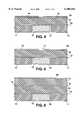
- FIG. 1is a cross-sectional view of a conductive region formed within a dielectric layer and in which an interconnect structure of the preferred embodiment is subsequently fabricated thereon.
- FIG. 2is a cross-sectional view showing a deposition of a dielectric separation layer onto the structure of FIG. 1.
- FIG. 3is a cross-sectional view showing a deposition of a first low-.di-elect cons. dielectric ILD layer over the structure of FIG. 2 and a subsequent deposition of a first dielectric etch-stop layer over the first ILD layer.
- FIG. 4is a cross-sectional view showing a deposition of a patterned photoresist layer atop the structure of FIG. 3, in which a widow opening is formed to expose a portion of the underlying etch-stop layer.
- FIG. 5is a cross-sectional view showing the widow opening pattern of FIG. 4 being transferred on to the first etch-stop layer to define a via opening.
- FIG. 6is a cross-sectional view showing a deposition of a second low-.di-elect cons. dielectric ILD layer over the structure of FIG. 5 and a subsequent deposition of a second etch-stop layer over the second ILD dielectric layer.
- FIG. 7is a cross-sectional view showing a deposition of a patterned photoresist layer atop the structure of FIG. 6, in which another window opening is formed to expose a portion of the underlying second etch-stop layer.
- FIG. 8is a cross-sectional view showing the window opening pattern of FIG. 7 being transferred on to the second etch-stop layer to define a trench opening.
- FIG. 9is a cross-sectional view showing an anisotropic etching of the first and second low-.di-elect cons. dielectric ILD layers of FIG. 8 in which the etching is performed through the trench and via openings.
- FIG. 10is a cross-sectional view showing an etching of the exposed separation layer at the bottom of the via opening shown in FIG. 9.
- FIG. 11is a cross-sectional view of a deposition of a conformal barrier layer on the structure shown in FIG. 10 and a subsequent deposition of a conductive material to fill in the via and trench openings.
- FIG. 12is across-sectional view showing the removal of the excess barrier layer and conductive materials residing on the surface for the structure of FIG. 11 by performing chemical-mechanical polishing.
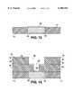
- FIG. 13is a cross-sectional view of a structure of an alternative embodiment that is equivalent to the structure shown in FIG. 2, but in which a conductive barrier layer is selectively deposited only onto the underlying conductive region.
- FIG. 14is a cross-sectional view of a structure that is equivalent to the structure shown in FIG. 10, but in which the selectively deposited conductive barrier layer of FIG. 13 is employed.
- FIG. 15is a cross-sectional view of a structure that is equivalent to the structure shown in FIG. 11, but in which the selectively deposited conductive barrier layer of FIG. 13 is employed.
- FIG. 16a cross-sectional view of a structure that is equivalent to the structure shown in FIG. 12, but in which the selectively deposited conductive barrier layer of FIG. 13 is employed.
- a technique for fabricating a dual damascene interconnect structure using a low dielectric constant material as a dielectric layer or layersis described.
- numerous specific detailsare set forth, such as specific structures, materials, processes, etc., in order to provide a thorough understanding of the present invention.
- the present inventionmay be practiced without these specific details.
- well known techniques and structureshave not been described in detail in order not to obscure the present invention.
- the present inventionis described in reference to a dual damascene interconnect structure in which aluminum or copper is used as the metal for the interconnect.
- other structures and conductive materialscan be readily implemented without departing from the spirit and scope of the present invention.
- the conductive region 10is comprised of a conductive material which can be of any of a variety of materials used for forming interconnects on a semiconductor wafer, such as a silicon wafer.
- a metalsuch as aluminum (Al) or its alloy, is used for forming the conductive regions on a wafer.
- the dielectric layer 11is formed from a dielectric material, which is typically used to form an inter-level dielectric (ILD) layer.
- ILDinter-level dielectric
- the conductive region 10 (hereinafter also referred to as interconnect 10) formed in the dielectric layer 11is shown in the Figure as a wiring interconnect.
- Wiring interconnectsare conductive regions formed within trenches and provide the wiring (or lines) for a given metallization layer on a semiconductor wafer.
- a plug interconnectis a conductive region formed within a via and provides the interconnection between the different metallization levels.
- Aluminumhas been used extensively for both trenches and vias. Other metals, such as tungsten, have been used as well for vias.
- copperhas higher resistance to electromigration and lower electrical resistivity than aluminum, it is a more preferred material for interconnect wiring than aluminum.
- copperhas lower resistivity than tungsten or aluminum, making copper a desirable metal for use in forming plugs.
- copperbecause of its diffusion property in the dielectric material and incompatibility with silicon materials, copper requires encapsulation to isolate it from most adjacent materials.
- barrier or encapsulation layeris required to prevent the copper from interacting with the surrounding material.
- the adjacent materialis fabricated from a silicon-based dielectric or a low-.di-elect cons. dielectric material.
- a liner layer 12 of some sortis desirable as well, when the adjacent material is formed from a low-.di-elect cons. dielectric.
- the liner layer 12functions as an adhesion promoter layer or a combination of barrier/adhesion promoter layer between the aluminum and the low-.di-elect cons. dielectric material.
- the conductive region 10is comprised of either aluminum or copper, some form of intervening liner layer 12 is needed to function as an adhesion promoter layer or a barrier layer that also functions as an adhesion promoter layer (hereinafter, it is understood that a barrier layer also provides adhesion promotion as well).
- Copperrequires a barrier layer.
- Aluminumonly requires an adhesion promoter layer, if the aluminum does not interact with the surrounding material. In the event aluminum does interact with the surrounding material, a barrier layer is required.
- the example shown in FIG. 1is described having either copper or aluminum as the material comprising the conductive region (or interconnect) 10.
- the interconnect 10can be comprised of other materials as well and is not limited to just copper and aluminum.
- region 10is part of a lower metallization layer (wiring interconnect), however, it is appreciated that the region 10 can be a plug interconnect or a doped region for the practice of the present invention.
- the dielectric layer 11can be comprised of an oxide (such as silicon dioxide (SiO 2 )), nitride or a low-.di-elect cons. dielectric.
- the dielectric material of layer 11will be a low-.di-elect cons. dielectric, since that is the preferred material for ILDs in the practice of the present invention.
- the low-.di-elect cons. dielectric selectedis an organic low-.di-elect cons. dielectric material.
- a barrier layer(also referred to as encapsulation or isolation layer) is used for the liner layer 12, when copper is used as the material comprising conductive region 10.
- the liner layer 12 in the example structurecan be formed from a variety of known barrier materials, including TiN, Ta, TaN, W, WN, SiN and WSiN. Again, it is appreciated that these materials also operate as an adhesion promoter. Generally, TiN or TaN is preferred when the interconnect 10 is comprised of copper.
- the liner layer 12can be a barrier layer or just an adhesion promoter layer (not having barrier properties), depending on the interaction of the aluminum to the surrounding material.
- a variety of known materialsincluding TiN, TiSiN, Ta, TaN, TaSiN, WN, SiO 2 , SiN, Al 2 O 3 , SiC and SiON, for example, can be used as a barrier/adhesion promoter material. Titanium can also be used strictly as an adhesion promoter material.
- the liner layer 12can be comprised of multiple layers. For example, a barrier material formed above an adhesion promoter layer.
- FIG. 1illustrates the starting structure upon which the various layers are formed to fabricate an interconnect structure of the present invention.
- a dielectric separation layer 13is deposited over the interconnect 10 and dielectric layer 11 (the dielectric layer 11 is henceforth referred to as an ILD layer 11 in order to differentiate the various dielectric layers being described).
- a variety of dielectric materialscan be used to form the dielectric separation layer 13 to separate the structure of FIG. 1 from the subsequently deposited overlying low-.di-elect cons. material. If the conductive region 10 is comprised of copper, then region 10 will need to be encapsulated. Accordingly, a barrier material, from the list of barrier materials described previously in reference to the liner layer 12, is used to form a barrier as layer 13.
- layer 13can be a barrier or an adhesion promoter layer, or both.
- silicon nitride (SiN)is deposited by chemical-vapor deposition (CVD) to an approximate thickness of 300-1000 angstroms when copper is used.
- SiN or SiO 2is deposited by CVD to an approximate thickness of 300-1000 angstroms.
- a primary purpose of the separation layer 13is to cap the exposed conductive region 10 for the subsequent ILD deposition. Functionally, the separation layer 13 functions equivalently to the liner layer 12 in isolating or separating the conductive material from the adjacent ILD.
- a first low-dielectric constant (low-.di-elect cons.) dielectric layer 14(hereinafter also referred to as the ILD layer 14) is deposited over the dielectric separation layer 13.
- the low-.di-elect cons. dielectric ILD layer 14 of the preferred embodimentis comprised of an organic low-.di-elect cons. material.
- organic low-.di-elect cons. dielectric materialare polyimide, fluorinated polyimide, parylene, poly-arylethers, fluorinated poly-arylethers and other polymers. However, this is not an inclusive list and other low-.di-elect cons. dielectric materials can be used as well.
- the low-.di-elect cons. layer 14is preferably deposited by CVD or a spin-on process to an approximate thickness of 5000-10,000 angstroms.
- etch-stop layer 15is deposited over the low-.di-elect cons. ILD layer 14.
- SiO 2is deposited by a CVD process to an approximate thickness of 300-1000 angstroms. As explained below, it is important that the material selected for the etch-stop layer 15 is different from that comprising the separation layer 13.
- photoresistive material 16is deposited, exposed and developed by the use of known techniques to form an opening to define a subsequent via hole opening.
- the photolithography techniqueexposes the location where portions of the dielectric layer 15 is to be etched.
- a plasma etch stepis utilized to remove the exposed portion of the dielectric layer 15 to form an opening 17. Accordingly, the pattern in the photoresist layer 16 is transferred to the dielectric layer 15 for forming the opening 17. Later, the opening 17 will define a location where the via hole opening is to be formed in the underlying low-.di-elect cons. layer 14.
- an anisotropic photoresist strip etch using O 2 plasmais used to remove the remaining photoresistive material 16.
- a high-density plasma etch utilizing low pressure, typically less than 5 mTorrcan be used for this step.
- the resulting structureis shown in FIG. 5. It is to be noted that the photoresist strip step can cause the removal of some of the low-.di-elect cons. material of layer 14 residing below the opening 17, as shown in FIG. 5. However, since another low-.di-elect cons. material layer will be deposited and planarized, such partial etching of the low-.di-elect cons. material at the particular location is not a concern.
- a second low-.di-elect cons. dielectric layer 18(hereinafter also referred to as the ILD layer 18) is deposited.
- This second low-.di-elect cons. ILD layer 18is equivalent to the first low-.di-elect cons. ILD layer 14 in the material and the technique in which it is formed.
- a typical thickness for the ILD layer 18is in the approximate range of 3000-8000 angstroms.
- etch-stop layer 19is deposited. It is again important to note that this second etch-stop layer 19 be comprised of a different material than the dielectric separation layer 13.
- the etch-stop layer 19can be comprised of the same material as the first etch-stop layer 15.
- the two etch-stop layersare comprised from the same material, but this material must be different from the material comprising the separation layer 13.
- SiO 2is used as the material for etch-stop layers 15 and 19.
- the dielectric etch-stop layer 19 thicknessis in the approximate range of 300-1000 angstroms.
- the via to the underlying conductive region 10is formed in the first low-.di-elect cons. ILD layer 14, while the trench is formed above the via in the second low-.di-elect cons. ILD layer 18. Accordingly, the three dielectric layers 13, 15 and 19 form the boundaries for the two ILD layers 14 and 18.
- the first and second etch-stop layers 15 and 19should have high etch selectivity in respect to the low-.di-elect cons. ILD layers 14 and 18.
- the two etch-stop layers 15 and 19should also have high etch selectivity with respect to the separation layer 13, as noted previously.
- photoresistive material 22is deposited, exposed and developed by the use of known techniques to form an opening to define a subsequent trench opening.
- the photolithography techniqueexposes the location where portions of the etch-stop layer 19 is to be etched.
- a plasma etch stepis utilized again to remove the exposed portion of the etch-stop layer 19 to form an opening 23 (shown in FIG. 8).
- the pattern in the photoresist layer 22is transferred to the etch-stop layer 19 for forming opening 23.
- the opening 23will define a location where the trench opening is to be formed in the underlying low-.di-elect cons. ILD layer 18.
- an anisotropic photoresist strip etch using O 2 plasmais used to remove the remaining photoresistive material 22.
- the resulting structureis shown in FIG. 8.
- the processis continued until the structure shown in FIG. 9 is achieved.
- This anisotropic etchwill continue to etch the exposed low-.di-elect cons. material in both of the ILD layers 14 and 18, but will not etch away the dielectric etch-stop layers 15 and 19.
- the two etch-stop layers 15 and 19function as etch-stops for the anisotropic etch of the low-.di-elect cons. dielectric material, so that only the exposed ILD region underlying the two openings 17 and 23 are etched.
- the resulting structureis a dual damascene structure illustrated in FIG. 9.
- the structure shown in FIG. 9is comprised of two layers of low-.di-elect cons. ILD material, having a via hole opening 24 and a trench opening 25.
- the via and trench openings 24 and 25correspond to the openings 17 and 23, respectively.
- both openings 24 and 25overly the interconnect 10.
- the dielectric separation layer 13is still intact at the bottom of the via 24.
- the etch chemistryis changed to etch the exposed portion of the separation layer 13 at the bottom of the via 24.
- the etch chemistry selectedmust be highly selective so that it will etch the exposed barrier or adhesion promoter material of the separation layer 13 at the bottom, but will not etch the two etch-stop layers 15 and 19 and the ILD material underlying them. This is the reason why the etch-stop layers 15 and 19 need to be comprised of a different material(s) than that selected for the separation layer 13. Thus, by the proper selection of the dielectric materials, such etch selectivity can be obtained.
- SiNis selected for the material comprising the separation layer 13 and SiO 2 is selected as the material comprising the two etch-stop layers 15 and 19.
- a CH 3 F/O 2 anisotropic etch chemistryis employed to etch away the exposed SiN material of layer 13, but the SiO 2 material of the layers 15 and 19 will not be etched.
- the presence of the SiO 2 etch-stop layersprotects the underlying low-.di-elect cons. dielectric material from being etched away by the O 2 component of the etch chemistry.
- the resulting structure after this etching stepis shown in FIG. 10.
- anisotropic O 2 etch cleanit is preferred at this stage to perform a similar anisotropic O 2 etch clean as previously mentioned to remove polymers at the bottom of the via (which may be generated during the layer 13 etch at the bottom of the via 24) and also to remove any photoresist that may remain on the surface.
- This type of cleanis preferred since most organic low-.di-elect cons. materials are not compatible to wet cleans.
- the remaining material of layers 15 and 19ensure that the underlying low-.di-elect cons. material will not be etched during the anisotropic O 2 clean etch.
- a barrier materialis conformally deposited to form a barrier (or encapsulation) layer 28 along the exposed surface of the structure of FIG. 10.
- the barrier layeris comprised of a metallic material.
- a purpose of the barrier layer 28is to provide a barrier between the surrounding low-.di-elect cons. material of ILD layers 14 and 18 and the copper or aluminum material which will fill in the via and trench openings. Since the conductive region 10 is exposed at the bottom of the via opening 24, the barrier layer 28 also provides a barrier between it and the material filling in the overlying via 24 if such a barrier is required.
- a variety of known barrier materialscan be utilized, in which the barrier material is deposited to an approximate thickness of 100-1000 angstroms.
- TiN or TaNis selected as the barrier metal for copper or aluminum fill. It is appreciated that the barrier layer 28 is functionally equivalent to the afore-mentioned liner layer 12. Accordingly, The previous description relating to the liner layer 12 applies to the layer 28 as well.
- conductive material 29is deposited to fill in the via and trench openings 24 and 25.
- the material depositedis comprised of either copper or aluminum, but it is understood that other metals could be readily used as well. Copper is the more preferred material, due to its enhanced properties over aluminum.
- copperis blanket deposited by a known PVD, CVD, plating technique, or a combination of these techniques to fill in the openings 24 and 25. It is appreciated that how the metal is deposited in the openings 24 and 25 is a design choice dependent on the fabrication process being employed.
- CMPchemical-mechanical polishing
- layer 19is described as a dielectric layer and the preference is to have this layer 19 be dielectric, it is possible to employ a metal material for layer 19. In the event layer 19 is a metal layer, then this CMP step will need to remove the remaining layer 19 completely, so that no metal trace remains along the top surface of the structure. Thus, if the layer 19 is dielectric, it can be fabricated into the final structure. However, if the layer 19 is metal, it must be removed completely, so that it will not be fabricated as part of the finished device.
- another dielectric layer 30is deposited over the structure to form a final covering layer over the exposed metal material 29 in the trench, as well as over the top surface of the structure (whether layer 19 is present or not).
- the trench and viaare completely filled and fully encapsulated.
- the dielectric layer 30is equivalent in material and function to the separation layer 13. That is, the filled trench region now operates as the underlying conductive region (equivalent to region 10) as the process of the present invention is repeated to form another interconnect structure of a subsequent level atop the present metallization level.
- additional interconnect structurescan be fabricated to form additional metallization level(s) above the structure shown in FIG. 12.
- the practice of the present inventionresults in the fabrication of a dual damascene structure, in which dual low-.di-elect cons. dielectric material layers form the ILD portion of an interconnect.
- dual low-.di-elect cons. dielectric material layersform the ILD portion of an interconnect.
- low-.di-elect cons. dielectric materialscan be used for the ILD layers 14 and 18, the preference is to use an organic low-.di-elect cons. dielectric material.
- the thickness of the lower layer 14determines the height of the via, while the thickness of the upper layer 18 determines the height of the trench.
- the total ILD heightis in the approximate range of 10,000-20,000 angstroms, but this height is a design choice.
- the materials selected for these layersshould provide sufficient adhesion quality for the particular low-.di-elect cons. dielectric materials deposited. This is in addition to the properties of these layers described above. Furthermore, it is preferred to use the same low-.di-elect cons. dielectric material for both of the ILD layers 14 and 18, however, different low-.di-elect cons. dielectric materials can be used if desired.
- the conductive region 10is comprised of copper for the preferred technique of the alternative embodiment described herein.
- FIG. 13shows the foundation structure that is equivalent to the structure shown in FIG. 1.
- coppercomprises the material for the conductive region 10.
- the liner layer 12is a barrier layer.
- an encapsulation layer 33is selectively deposited only over the conductive region 10.
- the encapsulating layer 33is a conductive barrier layer, which will then provide an encapsulating (or barrier) cap atop the copper conductive region 10.
- a selective layer 33is formed atop the conductive region 10, instead of the blanket separation layer 13 (shown in FIG. 2). This encapsulation layer 33 caps the underlying conductive region 10 for the subsequent ILD deposition.
- the subsequent steps for forming the two low-.di-elect cons. ILD layers 14 and 18, the two etch-stop layers 15 and 19, and the etching of the via and trench openings 24 and 25are equivalent to the earlier described steps pertaining to FIGS. 3-10 (with the one exception that layer 33 is selectively formed in place of layer 13).
- the resulting structureis shown in FIG. 14.
- the structure of FIG. 14shows the formation of via and trench openings. The exposed portion of the encapsulation layer 33 at the bottom of the via is not etched and remains in place for the subsequent fills.
- a conforming barrier layer 28is deposited, followed by a copper deposition, in which the via and trench are copper filled.
- the structure of FIG. 15is equivalent to the structure of FIG. 11 (with the exception noted for layer 33), wherein the preferred metal is copper.
- the subsequent etching or polishing stepremoves the excess metal material above the surface of the structure.
- another encapsulation layer 34is selectively formed above the exposed copper in order to fully encapsulate the copper. Again, as previously stated, this encapsulation layer 34 will function as the lower encapsulation layer (equivalent to layer 33) for the next level of metallization.
- the layer 33be a conductive barrier layer.
- One barrier material for forming the barrier layer 34 (as well as layer 33)is cobalt tungsten phosphide (CoWP). CoWP is selectively deposited onto the exposed copper by a technique of electroless deposition.
- One technique for performing such CoWP depositionis described in a pending patent application titled "Use Of Cobalt Tungsten Phosphide As A Barrier Material For Copper Metallization;" Ser. No. 08/754,600; filed Nov. 20, 1996. Accordingly, either blanket or selective deposition of the separation layer can be employed in the practice of the present invention.
- a dual damascene interconnect structure using a low dielectric constant material for the dielectric portion of the structureis described. It is appreciated that the technique can be applied to fabricate and manufacture integrated circuit devices on a semiconductor wafer, such as a silicon wafer. It is also appreciated that the technique of the present invention can also be readily adapted to other areas, such as for the manufacture of flat panel displays.
Landscapes
- Engineering & Computer Science (AREA)
- Physics & Mathematics (AREA)
- Condensed Matter Physics & Semiconductors (AREA)
- General Physics & Mathematics (AREA)
- Computer Hardware Design (AREA)
- Microelectronics & Electronic Packaging (AREA)
- Power Engineering (AREA)
- Manufacturing & Machinery (AREA)
- Internal Circuitry In Semiconductor Integrated Circuit Devices (AREA)
Abstract
Description
Claims (12)
Priority Applications (2)
| Application Number | Priority Date | Filing Date | Title |
|---|---|---|---|
| US08/914,995US6100184A (en) | 1997-08-20 | 1997-08-20 | Method of making a dual damascene interconnect structure using low dielectric constant material for an inter-level dielectric layer |
| US09/052,215US6037664A (en) | 1997-08-20 | 1998-03-31 | Dual damascene interconnect structure using low dielectric constant material for an inter-level dielectric layer |
Applications Claiming Priority (1)
| Application Number | Priority Date | Filing Date | Title |
|---|---|---|---|
| US08/914,995US6100184A (en) | 1997-08-20 | 1997-08-20 | Method of making a dual damascene interconnect structure using low dielectric constant material for an inter-level dielectric layer |
Related Child Applications (1)
| Application Number | Title | Priority Date | Filing Date |
|---|---|---|---|
| US09/052,215DivisionUS6037664A (en) | 1997-08-20 | 1998-03-31 | Dual damascene interconnect structure using low dielectric constant material for an inter-level dielectric layer |
Publications (1)
| Publication Number | Publication Date |
|---|---|
| US6100184Atrue US6100184A (en) | 2000-08-08 |
Family
ID=25435057
Family Applications (2)
| Application Number | Title | Priority Date | Filing Date |
|---|---|---|---|
| US08/914,995Expired - LifetimeUS6100184A (en) | 1997-08-20 | 1997-08-20 | Method of making a dual damascene interconnect structure using low dielectric constant material for an inter-level dielectric layer |
| US09/052,215Expired - LifetimeUS6037664A (en) | 1997-08-20 | 1998-03-31 | Dual damascene interconnect structure using low dielectric constant material for an inter-level dielectric layer |
Family Applications After (1)
| Application Number | Title | Priority Date | Filing Date |
|---|---|---|---|
| US09/052,215Expired - LifetimeUS6037664A (en) | 1997-08-20 | 1998-03-31 | Dual damascene interconnect structure using low dielectric constant material for an inter-level dielectric layer |
Country Status (1)
| Country | Link |
|---|---|
| US (2) | US6100184A (en) |
Cited By (129)
| Publication number | Priority date | Publication date | Assignee | Title |
|---|---|---|---|---|
| US6181013B1 (en)* | 1999-06-25 | 2001-01-30 | Taiwan Semiconductor Manufacturing Company | Method for selective growth of Cu3Ge or Cu5Si for passivation of damascene copper structures and device manufactured thereby |
| US6184128B1 (en)* | 2000-01-31 | 2001-02-06 | Advanced Micro Devices, Inc. | Method using a thin resist mask for dual damascene stop layer etch |
| US6197681B1 (en)* | 1999-12-31 | 2001-03-06 | United Microelectronics Corp. | Forming copper interconnects in dielectric materials with low constant dielectrics |
| US6235629B1 (en)* | 1998-09-29 | 2001-05-22 | Sharp Kabushiki Kaisha | Process for producing a semiconductor device |
| US6239023B1 (en)* | 1999-05-27 | 2001-05-29 | Taiwan Semiconductor Manufacturing Company | Method to reduce the damages of copper lines |
| US6239026B1 (en)* | 1998-09-28 | 2001-05-29 | Conexant Systems, Inc. | Nitride etch stop for poisoned unlanded vias |
| US6268283B1 (en)* | 1999-01-06 | 2001-07-31 | United Microelectronics Corp. | Method for forming dual damascene structure |
| WO2001063659A1 (en)* | 2000-02-24 | 2001-08-30 | Conexant Systems, Inc. | Method for fabrication and structure for high aspect ratio vias |
| US6291887B1 (en)* | 1999-01-04 | 2001-09-18 | Advanced Micro Devices, Inc. | Dual damascene arrangements for metal interconnection with low k dielectric constant materials and nitride middle etch stop layer |
| US6291891B1 (en)* | 1998-01-13 | 2001-09-18 | Kabushiki Kaisha Toshiba | Semiconductor device manufacturing method and semiconductor device |
| US6326301B1 (en)* | 1999-07-13 | 2001-12-04 | Motorola, Inc. | Method for forming a dual inlaid copper interconnect structure |
| US6331479B1 (en)* | 1999-09-20 | 2001-12-18 | Chartered Semiconductor Manufacturing Ltd. | Method to prevent degradation of low dielectric constant material in copper damascene interconnects |
| US6333258B1 (en)* | 1999-03-29 | 2001-12-25 | Sony Corporation | Method of manufacturing a semiconductor device |
| US20020030191A1 (en)* | 1998-08-28 | 2002-03-14 | Das Mrinal Kanti | High voltage, high temperature capacitor structures and methods of fabricating same |
| US6358842B1 (en)* | 2000-08-07 | 2002-03-19 | Chartered Semiconductor Manufacturing Ltd. | Method to form damascene interconnects with sidewall passivation to protect organic dielectrics |
| US6380073B1 (en)* | 2000-08-29 | 2002-04-30 | United Microelectronics Corp. | Method for forming metal interconnection structure without corner faceted |
| US6380091B1 (en)* | 1999-01-27 | 2002-04-30 | Advanced Micro Devices, Inc. | Dual damascene arrangement for metal interconnection with oxide dielectric layer and low K dielectric constant layer |
| US6384480B1 (en)* | 1999-02-18 | 2002-05-07 | Micron Technology, Inc. | Formation of electrical contacts to conductive elements in the fabrication of semiconductor integrated circuits |
| US6383919B1 (en)* | 2001-02-07 | 2002-05-07 | Advanced Micro Devices, Inc. | Method of making a dual damascene structure without middle stop layer |
| US6391785B1 (en)* | 1999-08-24 | 2002-05-21 | Interuniversitair Microelektronica Centrum (Imec) | Method for bottomless deposition of barrier layers in integrated circuit metallization schemes |
| US6406996B1 (en)* | 2000-09-30 | 2002-06-18 | Advanced Micro Devices, Inc. | Sub-cap and method of manufacture therefor in integrated circuit capping layers |
| US6424038B1 (en) | 2001-03-19 | 2002-07-23 | Taiwan Semiconductor Manufacturing Co., Ltd | Low dielectric constant microelectronic conductor structure with enhanced adhesion and attenuated electrical leakage |
| US6429129B1 (en)* | 2000-06-16 | 2002-08-06 | Chartered Semiconductor Manufacturing Ltd. | Method of using silicon rich carbide as a barrier material for fluorinated materials |
| US6440840B1 (en) | 2002-01-25 | 2002-08-27 | Taiwan Semiconductor Manufactoring Company | Damascene process to eliminate copper defects during chemical-mechanical polishing (CMP) for making electrical interconnections on integrated circuits |
| US6440838B1 (en) | 2001-11-20 | 2002-08-27 | Taiwan Semiconductor Manufacturing Co., Ltd | Dual damascene structure employing laminated intermediate etch stop layer |
| US20020123215A1 (en)* | 1999-02-17 | 2002-09-05 | Ulvac Inc. | Process for producing barrier film and barrier film thus produced |
| US6455415B1 (en)* | 1999-04-21 | 2002-09-24 | Advanced Micro Devices, Inc. | Method of encapsulated copper (Cu) interconnect formation |
| US20020158337A1 (en)* | 2000-02-08 | 2002-10-31 | Babich Katherina E. | Multilayer interconnect structure containing air gaps and method for making |
| US6475912B1 (en)* | 1998-06-01 | 2002-11-05 | Matsushita Electric Industrial Co., Ltd. | Semiconductor device and method and apparatus for fabricating the same while minimizing operating failures and optimizing yield |
| US6498399B2 (en)* | 1999-09-08 | 2002-12-24 | Alliedsignal Inc. | Low dielectric-constant dielectric for etchstop in dual damascene backend of integrated circuits |
| WO2002103790A1 (en)* | 2001-06-18 | 2002-12-27 | Infineon Technologies North America Corp. | Reduction of via-resistance-shift by increasing via size at a last conductor level of a semiconductor device |
| US6511909B1 (en)* | 1998-02-11 | 2003-01-28 | Applied Materials, Inc. | Method of depositing a low K dielectric with organo silane |
| US6514857B1 (en)* | 1998-02-02 | 2003-02-04 | Applied Materials, Inc. | Damascene structure fabricated using a layer of silicon-based photoresist material |
| US6518166B1 (en)* | 2001-04-23 | 2003-02-11 | Taiwan Semiconductor Manufacturing Company | Liquid phase deposition of a silicon oxide layer for use as a liner on the surface of a dual damascene opening in a low dielectric constant layer |
| US6531780B1 (en)* | 2001-06-27 | 2003-03-11 | Advanced Micro Devices, Inc. | Via formation in integrated circuit interconnects |
| US6534835B2 (en) | 2000-08-28 | 2003-03-18 | Micron Technology, Inc. | Damascene structure with low dielectric constant insulating layers |
| US6551930B1 (en)* | 2000-06-07 | 2003-04-22 | Stmicroelectronics S.A. | Etching an organic material layer, particularly for producing interconnections of the damascene type |
| US6562725B2 (en) | 2001-07-05 | 2003-05-13 | Taiwan Semiconductor Manufacturing Co., Ltd | Dual damascene structure employing nitrogenated silicon carbide and non-nitrogenated silicon carbide etch stop layers |
| US20030119317A1 (en)* | 2000-10-12 | 2003-06-26 | Takeshi Nogami | Semiconductor device and production method therefor |
| US6589863B1 (en)* | 1998-12-25 | 2003-07-08 | Nec Electronics Corp. | Semiconductor device and manufacturing method thereof |
| US6594540B1 (en)* | 1998-07-10 | 2003-07-15 | Applied Materials, Inc. | Misalignment tolerant techniques for dual damascene fabrication |
| US20030148604A1 (en)* | 2001-12-13 | 2003-08-07 | Mou-Shiung Lin | Chip structure and process for forming the same |
| US6605874B2 (en)* | 2001-12-19 | 2003-08-12 | Intel Corporation | Method of making semiconductor device using an interconnect |
| US6620727B2 (en)* | 2001-08-23 | 2003-09-16 | Texas Instruments Incorporated | Aluminum hardmask for dielectric etch |
| US6627539B1 (en)* | 1998-05-29 | 2003-09-30 | Newport Fab, Llc | Method of forming dual-damascene interconnect structures employing low-k dielectric materials |
| US20030190426A1 (en)* | 2002-04-03 | 2003-10-09 | Deenesh Padhi | Electroless deposition method |
| US20030207594A1 (en)* | 2001-06-19 | 2003-11-06 | Catabay Wilbur G. | Plasma treatment of low dielectric constant dielectric material to form structures useful in formation of metal interconnects and/or filled vias for intergrated circuit structure |
| US20030219991A1 (en)* | 2000-08-25 | 2003-11-27 | Micron Technology, Inc. | Conductive material patterning methods |
| US6680540B2 (en) | 2000-03-08 | 2004-01-20 | Hitachi, Ltd. | Semiconductor device having cobalt alloy film with boron |
| US6689695B1 (en)* | 2002-06-28 | 2004-02-10 | Taiwan Semiconductor Manufacturing Company | Multi-purpose composite mask for dual damascene patterning |
| US20040038507A1 (en)* | 1998-09-23 | 2004-02-26 | Infineon Technologies Ag | Method of producing an integrated circuit configuration |
| US20040061236A1 (en)* | 2002-09-30 | 2004-04-01 | Sanyo Electric Co., Ltd. | Semiconductor device provided with a dielectric film including porous structure and manufacturing method thereof |
| US6727169B1 (en)* | 1999-10-15 | 2004-04-27 | Asm International, N.V. | Method of making conformal lining layers for damascene metallization |
| US6734110B1 (en)* | 1999-10-14 | 2004-05-11 | Taiwan Semiconductor Manufacturing Company | Damascene method employing composite etch stop layer |
| US6734559B1 (en)* | 1999-09-17 | 2004-05-11 | Advanced Micro Devices, Inc. | Self-aligned semiconductor interconnect barrier and manufacturing method therefor |
| US6737222B2 (en)* | 2000-11-21 | 2004-05-18 | Advanced Micro Devices, Inc. | Dual damascene process utilizing a bi-layer imaging layer |
| US20040102031A1 (en)* | 2002-11-21 | 2004-05-27 | Kloster Grant M. | Low-K dielectric structure and method |
| US20040108217A1 (en)* | 2002-12-05 | 2004-06-10 | Dubin Valery M. | Methods for forming copper interconnect structures by co-plating of noble metals and structures formed thereby |
| US20040123921A1 (en)* | 2002-12-27 | 2004-07-01 | Park Sang Kyun | Plate for forming metal wires and method of forming metal wires using the same |
| US6764939B1 (en)* | 1999-03-09 | 2004-07-20 | Tokyo Electron Limited | Semiconductor device and method of manufacturing the same |
| WO2004053948A3 (en)* | 2002-12-09 | 2004-08-19 | Advanced Micro Devices Inc | Air gap dual damascene process and structure |
| US20040161535A1 (en)* | 2003-02-13 | 2004-08-19 | Goundar Kamal Kishore | Method of forming silicon carbide films |
| US20040166676A1 (en)* | 2002-09-12 | 2004-08-26 | Tetsunori Kaji | Method and apparatus for forming damascene structure, and damascene structure |
| US20040175923A1 (en)* | 2003-02-24 | 2004-09-09 | Nec Electronics Corporation | Semiconductor device and fabrication thereof |
| US20040219783A1 (en)* | 2001-07-09 | 2004-11-04 | Micron Technology, Inc. | Copper dual damascene interconnect technology |
| US6815332B2 (en) | 2002-10-30 | 2004-11-09 | Asm Japan K.K. | Method for forming integrated dielectric layers |
| US20040241978A1 (en)* | 2003-05-29 | 2004-12-02 | Chiung-Sheng Hsiung | Interconnection structure and fabrication method thereof |
| US6833318B2 (en)* | 2002-11-20 | 2004-12-21 | United Microelectronics Corp. | Gap-filling process |
| US6841467B2 (en)* | 2000-04-25 | 2005-01-11 | Sharp Kabushiki Kaisha | Method for producing semiconductor device |
| KR100475931B1 (en)* | 2002-07-02 | 2005-03-10 | 매그나칩 반도체 유한회사 | Method for manufacturing a multi metal line in semiconductor device |
| US20050059231A1 (en)* | 2000-10-26 | 2005-03-17 | Matsushita Electric Industrial Co., Ltd. | Semiconductor device and method for fabricating the same |
| US20050087844A1 (en)* | 1998-12-21 | 2005-04-28 | Mou-Shiung Lin | Chip structure and process for forming the same |
| US20050095830A1 (en)* | 2003-10-17 | 2005-05-05 | Applied Materials, Inc. | Selective self-initiating electroless capping of copper with cobalt-containing alloys |
| US20050101130A1 (en)* | 2003-11-07 | 2005-05-12 | Applied Materials, Inc. | Method and tool of chemical doping CoW alloys with Re for increasing barrier properties of electroless capping layers for IC Cu interconnects |
| US20050124158A1 (en)* | 2003-10-15 | 2005-06-09 | Lopatin Sergey D. | Silver under-layers for electroless cobalt alloys |
| US20050136193A1 (en)* | 2003-10-17 | 2005-06-23 | Applied Materials, Inc. | Selective self-initiating electroless capping of copper with cobalt-containing alloys |
| US20050136185A1 (en)* | 2002-10-30 | 2005-06-23 | Sivakami Ramanathan | Post rinse to improve selective deposition of electroless cobalt on copper for ULSI application |
| US20050164497A1 (en)* | 2004-01-26 | 2005-07-28 | Sergey Lopatin | Pretreatment for electroless deposition |
| US20050161338A1 (en)* | 2004-01-26 | 2005-07-28 | Applied Materials, Inc. | Electroless cobalt alloy deposition process |
| US6958547B2 (en) | 2002-05-03 | 2005-10-25 | Intel Corporation | Interconnect structures containing conductive electrolessly deposited etch stop layers, liner layers, and via plugs |
| US20050266673A1 (en)* | 1999-07-27 | 2005-12-01 | International Business Machines Corporation | Reduced electromigration and stressed induced migration of copper wires by surface coating |
| US20050263900A1 (en)* | 1998-11-17 | 2005-12-01 | Applied Materials, Inc. | Semiconductor device having silicon carbide and conductive pathway interface |
| US6977224B2 (en) | 2000-12-28 | 2005-12-20 | Intel Corporation | Method of electroless introduction of interconnect structures |
| US7071564B1 (en) | 2004-03-04 | 2006-07-04 | Advanced Micro Devices, Inc. | Composite tantalum capped inlaid copper with reduced electromigration and reduced stress migration |
| US20060160354A1 (en)* | 2003-10-23 | 2006-07-20 | Chartered Semiconductor Manufacturing Ltd. | Via electromigration improvement by changing the via bottom geometric profile |
| US20060162658A1 (en)* | 2005-01-27 | 2006-07-27 | Applied Materials, Inc. | Ruthenium layer deposition apparatus and method |
| US20060165892A1 (en)* | 2005-01-27 | 2006-07-27 | Applied Materials, Inc. | Ruthenium containing layer deposition method |
| US7087104B2 (en) | 2003-06-26 | 2006-08-08 | Intel Corporation | Preparation of electroless deposition solutions |
| US20060205194A1 (en)* | 2005-02-04 | 2006-09-14 | Matthias Bauer | Methods of depositing electrically active doped crystalline Si-containing films |
| US7122465B1 (en)* | 2004-12-02 | 2006-10-17 | Spansion Llc | Method for achieving increased control over interconnect line thickness across a wafer and between wafers |
| US20060276027A1 (en)* | 2005-06-06 | 2006-12-07 | Taiwan Semiconductor Manufacturing Co., Ltd. | Interconnects with harmonized stress and methods for fabricating the same |
| US20060286306A1 (en)* | 2005-06-17 | 2006-12-21 | Asm Japan K.K. | Method of producing advanced low dielectric constant film by UV light emission |
| US7192867B1 (en)* | 2002-06-26 | 2007-03-20 | Cypress Semiconductor Corporation | Protection of low-k dielectric in a passivation level |
| US20070071888A1 (en)* | 2005-09-21 | 2007-03-29 | Arulkumar Shanmugasundram | Method and apparatus for forming device features in an integrated electroless deposition system |
| US20070096326A1 (en)* | 2005-10-28 | 2007-05-03 | Taiwan Semiconductor Manufacturing Co., Ltd. | Semiconductor device and fabrication method thereof |
| US20070155079A1 (en)* | 2005-12-29 | 2007-07-05 | Dae Kyeun Kim | Gate structure of semiconductor device and method of manufacturing the same |
| US20070161216A1 (en)* | 2005-12-22 | 2007-07-12 | Matthias Bauer | Epitaxial deposition of doped semiconductor materials |
| US20070173062A1 (en)* | 2006-01-23 | 2007-07-26 | Micron Technology, Inc. | Method of cleaning a surface of a cobalt-containing material, method of forming an opening to a cobalt-containing material, semiconductor processing method of forming an integrated circuit comprising a copper-containing conductive line, and a cobalt-containing film cleaning solution |
| US20070260097A1 (en)* | 2005-03-18 | 2007-11-08 | Senkevich John J | Deposition of Polymeric Materials and Precursors Therefor |
| US20070287294A1 (en)* | 2006-06-08 | 2007-12-13 | Taiwan Semiconductor Manufacturing Co., Ltd. | Interconnect structures and methods for fabricating the same |
| US20080066778A1 (en)* | 2006-09-19 | 2008-03-20 | Asm Japan K.K. | Method of cleaning uv irradiation chamber |
| US20080067681A1 (en)* | 2006-09-19 | 2008-03-20 | National Tsing Hua University | Interconnection structure and manufacturing method thereof |
| US20080073645A1 (en)* | 2001-02-12 | 2008-03-27 | Asm America, Inc. | Thin films and methods of making them |
| US20080146019A1 (en)* | 2001-12-13 | 2008-06-19 | Megica Corporation | Chip structure and process for forming the same |
| US20080182406A1 (en)* | 2007-01-31 | 2008-07-31 | Axel Preusse | Method of forming a copper-based metallization layer including a conductive cap layer by an advanced integration regime |
| US20080217777A1 (en)* | 2005-09-13 | 2008-09-11 | International Business Machines Corporation | Embedded barrier for dielectric encapsulation |
| US7514353B2 (en) | 2005-03-18 | 2009-04-07 | Applied Materials, Inc. | Contact metallization scheme using a barrier layer over a silicide layer |
| US20090093135A1 (en)* | 2007-10-04 | 2009-04-09 | Asm Japan K.K. | Semiconductor manufacturing apparatus and method for curing material with uv light |
| US20090098730A1 (en)* | 2005-11-25 | 2009-04-16 | Samsung Electronics Co., Ltd. | Semiconductor device and method of fabricating the same |
| US20090111246A1 (en)* | 2007-10-26 | 2009-04-30 | Asm America, Inc. | Inhibitors for selective deposition of silicon containing films |
| US20090163001A1 (en)* | 2007-12-21 | 2009-06-25 | Asm America, Inc. | Separate injection of reactive species in selective formation of films |
| US7651934B2 (en) | 2005-03-18 | 2010-01-26 | Applied Materials, Inc. | Process for electroless copper deposition |
| US7659203B2 (en) | 2005-03-18 | 2010-02-09 | Applied Materials, Inc. | Electroless deposition process on a silicon contact |
| US7759199B2 (en) | 2007-09-19 | 2010-07-20 | Asm America, Inc. | Stressor for engineered strain on channel |
| US20100244265A1 (en)* | 2007-12-12 | 2010-09-30 | Panasonic Corporation | Semiconductor device and method for manufacturing the same |
| USRE41842E1 (en)* | 1996-12-05 | 2010-10-19 | Samsung Electronics Co., Ltd. | Methods of forming electrical interconnects on integrated circuit substrates using selective slurries |
| US7863654B2 (en) | 1998-12-21 | 2011-01-04 | Megica Corporation | Top layers of metal for high performance IC's |
| US20110162875A1 (en)* | 2010-01-07 | 2011-07-07 | International Business Machines Corporation | Selective copper encapsulation layer deposition |
| US8278176B2 (en) | 2006-06-07 | 2012-10-02 | Asm America, Inc. | Selective epitaxial formation of semiconductor films |
| US8367528B2 (en) | 2009-11-17 | 2013-02-05 | Asm America, Inc. | Cyclical epitaxial deposition and etch |
| US8486191B2 (en) | 2009-04-07 | 2013-07-16 | Asm America, Inc. | Substrate reactor with adjustable injectors for mixing gases within reaction chamber |
| US8779596B2 (en) | 2000-01-18 | 2014-07-15 | Micron Technology, Inc. | Structures and methods to enhance copper metallization |
| US8809170B2 (en) | 2011-05-19 | 2014-08-19 | Asm America Inc. | High throughput cyclical epitaxial deposition and etch process |
| US8921205B2 (en) | 2002-08-14 | 2014-12-30 | Asm America, Inc. | Deposition of amorphous silicon-containing films |
| US9378976B2 (en) | 2014-04-02 | 2016-06-28 | Applied Materials, Inc. | Method for forming interconnects |
| US20180019162A1 (en)* | 2016-07-13 | 2018-01-18 | Globalfoundries Inc. | Amorphous carbon layer for cobalt etch protection in dual damascene back end of the line integrated circuit metallization integration |
| US20180166334A1 (en)* | 2016-12-14 | 2018-06-14 | Samsung Electronics Co., Ltd. | Semiconductor device |
| CN113314500A (en)* | 2020-04-22 | 2021-08-27 | 台湾积体电路制造股份有限公司 | Semiconductor structure and manufacturing method thereof |
| US20210335661A1 (en)* | 2020-04-22 | 2021-10-28 | Taiwan Semiconductor Manufacturing Company Limited | Semiconductor structure and method for forming the same |
Families Citing this family (138)
| Publication number | Priority date | Publication date | Assignee | Title |
|---|---|---|---|---|
| US6429120B1 (en) | 2000-01-18 | 2002-08-06 | Micron Technology, Inc. | Methods and apparatus for making integrated-circuit wiring from copper, silver, gold, and other metals |
| US6037257A (en)* | 1997-05-08 | 2000-03-14 | Applied Materials, Inc. | Sputter deposition and annealing of copper alloy metallization |
| US6577011B1 (en)* | 1997-07-10 | 2003-06-10 | International Business Machines Corporation | Chip interconnect wiring structure with low dielectric constant insulator and methods for fabricating the same |
| JP3660799B2 (en)* | 1997-09-08 | 2005-06-15 | 株式会社ルネサステクノロジ | Manufacturing method of semiconductor integrated circuit device |
| US6286939B1 (en)* | 1997-09-26 | 2001-09-11 | Hewlett-Packard Company | Method of treating a metal surface to increase polymer adhesion |
| SG70654A1 (en)* | 1997-09-30 | 2000-02-22 | Ibm | Copper stud structure with refractory metal liner |
| JPH11204523A (en)* | 1998-01-07 | 1999-07-30 | Toshiba Corp | Method for manufacturing semiconductor device |
| EP0933814A1 (en)* | 1998-01-28 | 1999-08-04 | Interuniversitair Micro-Elektronica Centrum Vzw | A metallization structure on a fluorine-containing dielectric and a method for fabrication thereof |
| US6576547B2 (en) | 1998-03-05 | 2003-06-10 | Micron Technology, Inc. | Residue-free contact openings and methods for fabricating same |
| US6455937B1 (en)* | 1998-03-20 | 2002-09-24 | James A. Cunningham | Arrangement and method for improved downward scaling of higher conductivity metal-based interconnects |
| JP3798908B2 (en)* | 1998-05-07 | 2006-07-19 | 三菱電機株式会社 | Semiconductor device and manufacturing method thereof |
| TW377492B (en)* | 1998-06-08 | 1999-12-21 | United Microelectronics Corp | Method of manufacturing dual damascene |
| TW407342B (en)* | 1998-06-17 | 2000-10-01 | United Microelectronics Corp | Planarization method of damascene structure |
| US6372633B1 (en)* | 1998-07-08 | 2002-04-16 | Applied Materials, Inc. | Method and apparatus for forming metal interconnects |
| KR100265771B1 (en)* | 1998-07-09 | 2000-10-02 | 윤종용 | Method for metallization by dual damascene process using photosensitive polymer |
| US6060383A (en)* | 1998-08-10 | 2000-05-09 | Nogami; Takeshi | Method for making multilayered coaxial interconnect structure |
| US6103616A (en)* | 1998-08-19 | 2000-08-15 | Advanced Micro Devices, Inc. | Method to manufacture dual damascene structures by utilizing short resist spacers |
| US6194128B1 (en)* | 1998-09-17 | 2001-02-27 | Taiwan Semiconductor Manufacturing Company | Method of dual damascene etching |
| US6171951B1 (en)* | 1998-10-30 | 2001-01-09 | United Microelectronic Corp. | Dual damascene method comprising ion implanting to densify dielectric layer and forming a hard mask layer with a tapered opening |
| US6268261B1 (en)* | 1998-11-03 | 2001-07-31 | International Business Machines Corporation | Microprocessor having air as a dielectric and encapsulated lines and process for manufacture |
| JP2000150644A (en)* | 1998-11-10 | 2000-05-30 | Mitsubishi Electric Corp | Method for manufacturing semiconductor device |
| US6515343B1 (en) | 1998-11-19 | 2003-02-04 | Quicklogic Corporation | Metal-to-metal antifuse with non-conductive diffusion barrier |
| TW406369B (en)* | 1998-12-18 | 2000-09-21 | United Microelectronics Corp | Method for manufacturing damascene |
| US6255233B1 (en)* | 1998-12-30 | 2001-07-03 | Intel Corporation | In-situ silicon nitride and silicon based oxide deposition with graded interface for damascene application |
| US20010013660A1 (en) | 1999-01-04 | 2001-08-16 | Peter Richard Duncombe | Beol decoupling capacitor |
| US6207576B1 (en)* | 1999-01-05 | 2001-03-27 | Advanced Micro Devices, Inc. | Self-aligned dual damascene arrangement for metal interconnection with low k dielectric constant materials and oxide etch stop layer |
| US6235628B1 (en)* | 1999-01-05 | 2001-05-22 | Advanced Micro Devices, Inc. | Method of forming dual damascene arrangement for metal interconnection with low k dielectric constant materials and oxide middle etch stop layer |
| TW445581B (en)* | 1999-03-03 | 2001-07-11 | Taiwan Semiconductor Mfg | Manufacturing method of metal interconnect |
| TW400619B (en)* | 1999-03-05 | 2000-08-01 | United Microelectronics Corp | The manufacture method of dual damascene structure |
| US6156642A (en)* | 1999-03-23 | 2000-12-05 | United Microelectronics Corp. | Method of fabricating a dual damascene structure in an integrated circuit |
| US6144099A (en)* | 1999-03-30 | 2000-11-07 | Advanced Micro Devices, Inc. | Semiconductor metalization barrier |
| JP2000311939A (en)* | 1999-04-27 | 2000-11-07 | Mitsubishi Electric Corp | Semiconductor device and manufacturing method thereof |
| US6248665B1 (en)* | 1999-07-06 | 2001-06-19 | Taiwan Semiconductor Manufacturing Company | Delamination improvement between Cu and dielectrics for damascene process |
| US6309964B1 (en)* | 1999-07-08 | 2001-10-30 | Taiwan Semiconductor Manufacturing Company | Method for forming a copper damascene structure over tungsten plugs with improved adhesion, oxidation resistance, and diffusion barrier properties using nitridation of the tungsten plug |
| US6140220A (en)* | 1999-07-08 | 2000-10-31 | Industrial Technology Institute Reseach | Dual damascene process and structure with dielectric barrier layer |
| US6521532B1 (en) | 1999-07-22 | 2003-02-18 | James A. Cunningham | Method for making integrated circuit including interconnects with enhanced electromigration resistance |
| US6551872B1 (en) | 1999-07-22 | 2003-04-22 | James A. Cunningham | Method for making integrated circuit including interconnects with enhanced electromigration resistance using doped seed layer and integrated circuits produced thereby |
| US7069101B1 (en) | 1999-07-29 | 2006-06-27 | Applied Materials, Inc. | Computer integrated manufacturing techniques |
| JP2001044202A (en)* | 1999-07-30 | 2001-02-16 | Nec Corp | Semiconductor device and manufacturing method thereof |
| US6495452B1 (en)* | 1999-08-18 | 2002-12-17 | Taiwan Semiconductor Manufacturing Company | Method to reduce capacitance for copper interconnect structures |
| US6441492B1 (en) | 1999-09-10 | 2002-08-27 | James A. Cunningham | Diffusion barriers for copper interconnect systems |
| US6156655A (en)* | 1999-09-30 | 2000-12-05 | United Microelectronics Corp. | Retardation layer for preventing diffusion of metal layer and fabrication method thereof |
| US6329701B1 (en)* | 1999-10-04 | 2001-12-11 | Advanced Micro Devices, Inc. | Semiconductor device comprising copper interconnects with reduced in-line diffusion |
| US6640151B1 (en)* | 1999-12-22 | 2003-10-28 | Applied Materials, Inc. | Multi-tool control system, method and medium |
| JP2001196380A (en)* | 2000-01-12 | 2001-07-19 | Mitsubishi Electric Corp | Semiconductor device and method of manufacturing the same |
| US7262130B1 (en)* | 2000-01-18 | 2007-08-28 | Micron Technology, Inc. | Methods for making integrated-circuit wiring from copper, silver, gold, and other metals |
| US6376370B1 (en)* | 2000-01-18 | 2002-04-23 | Micron Technology, Inc. | Process for providing seed layers for using aluminum, copper, gold and silver metallurgy process for providing seed layers for using aluminum, copper, gold and silver metallurgy |
| US6355555B1 (en)* | 2000-01-28 | 2002-03-12 | Advanced Micro Devices, Inc. | Method of fabricating copper-based semiconductor devices using a sacrificial dielectric layer |
| US20010015499A1 (en)* | 2000-02-23 | 2001-08-23 | Hiroshi Yuasa | Semiconductor device and method for fabricating the same |
| JP2001319928A (en)* | 2000-05-08 | 2001-11-16 | Hitachi Ltd | Semiconductor integrated circuit device and method of manufacturing the same |
| US6316351B1 (en)* | 2000-05-31 | 2001-11-13 | Taiwan Semiconductor Manufacturing Company | Inter-metal dielectric film composition for dual damascene process |
| KR100403454B1 (en)* | 2000-06-20 | 2003-11-01 | 주식회사 하이닉스반도체 | Method of forming a metal wiring in a semiconductor device |
| US6531777B1 (en)* | 2000-06-22 | 2003-03-11 | Advanced Micro Devices, Inc. | Barrier metal integrity testing using a dual level line to line leakage testing pattern and partial CMP |
| US6284619B1 (en) | 2000-06-29 | 2001-09-04 | International Business Machines Corporation | Integration scheme for multilevel metallization structures |
| JP3934343B2 (en)* | 2000-07-12 | 2007-06-20 | キヤノンマーケティングジャパン株式会社 | Semiconductor device and manufacturing method thereof |
| US6524944B1 (en)* | 2000-07-17 | 2003-02-25 | Advanced Micro Devices, Inc. | Low k ILD process by removable ILD |
| US6531407B1 (en) | 2000-08-31 | 2003-03-11 | Micron Technology, Inc. | Method, structure and process flow to reduce line-line capacitance with low-K material |
| JP3917355B2 (en)* | 2000-09-21 | 2007-05-23 | 株式会社東芝 | Semiconductor device and manufacturing method thereof |
| US6790722B1 (en)* | 2000-11-22 | 2004-09-14 | International Business Machines Corporation | Logic SOI structure, process and application for vertical bipolar transistor |
| US7188142B2 (en)* | 2000-11-30 | 2007-03-06 | Applied Materials, Inc. | Dynamic subject information generation in message services of distributed object systems in a semiconductor assembly line facility |
| US6462417B1 (en)* | 2000-12-18 | 2002-10-08 | Advanced Micro Devices, Inc. | Coherent alloy diffusion barrier for integrated circuit interconnects |
| US6441838B1 (en) | 2001-01-19 | 2002-08-27 | Hewlett-Packard Company | Method of treating a metal surface to increase polymer adhesion |
| US6448654B1 (en)* | 2001-01-29 | 2002-09-10 | Advanced Micro Devices, Inc. | Ultra thin etch stop layer for damascene process |
| US20020128735A1 (en)* | 2001-03-08 | 2002-09-12 | Hawkins Parris C.M. | Dynamic and extensible task guide |
| US7087997B2 (en) | 2001-03-12 | 2006-08-08 | International Business Machines Corporation | Copper to aluminum interlayer interconnect using stud and via liner |
| US20020138321A1 (en)* | 2001-03-20 | 2002-09-26 | Applied Materials, Inc. | Fault tolerant and automated computer software workflow |
| US6768204B1 (en)* | 2001-04-05 | 2004-07-27 | Advanced Micro Devices, Inc. | Self-aligned conductive plugs in a semiconductor device |
| US6514844B1 (en)* | 2001-04-23 | 2003-02-04 | Advanced Micro Devices, Inc. | Sidewall treatment for low dielectric constant (low K) materials by ion implantation |
| US6803314B2 (en)* | 2001-04-30 | 2004-10-12 | Chartered Semiconductor Manufacturing Ltd. | Double-layered low dielectric constant dielectric dual damascene method |
| US7082345B2 (en)* | 2001-06-19 | 2006-07-25 | Applied Materials, Inc. | Method, system and medium for process control for the matching of tools, chambers and/or other semiconductor-related entities |
| US7201936B2 (en)* | 2001-06-19 | 2007-04-10 | Applied Materials, Inc. | Method of feedback control of sub-atmospheric chemical vapor deposition processes |
| US20020192966A1 (en)* | 2001-06-19 | 2002-12-19 | Shanmugasundram Arulkumar P. | In situ sensor based control of semiconductor processing procedure |
| US7101799B2 (en) | 2001-06-19 | 2006-09-05 | Applied Materials, Inc. | Feedforward and feedback control for conditioning of chemical mechanical polishing pad |
| US7160739B2 (en)* | 2001-06-19 | 2007-01-09 | Applied Materials, Inc. | Feedback control of a chemical mechanical polishing device providing manipulation of removal rate profiles |
| US6910947B2 (en)* | 2001-06-19 | 2005-06-28 | Applied Materials, Inc. | Control of chemical mechanical polishing pad conditioner directional velocity to improve pad life |
| US7698012B2 (en) | 2001-06-19 | 2010-04-13 | Applied Materials, Inc. | Dynamic metrology schemes and sampling schemes for advanced process control in semiconductor processing |
| US6913938B2 (en)* | 2001-06-19 | 2005-07-05 | Applied Materials, Inc. | Feedback control of plasma-enhanced chemical vapor deposition processes |
| US7047099B2 (en)* | 2001-06-19 | 2006-05-16 | Applied Materials Inc. | Integrating tool, module, and fab level control |
| US6879046B2 (en)* | 2001-06-28 | 2005-04-12 | Agere Systems Inc. | Split barrier layer including nitrogen-containing portion and oxygen-containing portion |
| US7337019B2 (en)* | 2001-07-16 | 2008-02-26 | Applied Materials, Inc. | Integration of fault detection with run-to-run control |
| US6950716B2 (en)* | 2001-08-13 | 2005-09-27 | Applied Materials, Inc. | Dynamic control of wafer processing paths in semiconductor manufacturing processes |
| US20030037090A1 (en)* | 2001-08-14 | 2003-02-20 | Koh Horne L. | Tool services layer for providing tool service functions in conjunction with tool functions |
| US6984198B2 (en)* | 2001-08-14 | 2006-01-10 | Applied Materials, Inc. | Experiment management system, method and medium |
| US6559543B1 (en)* | 2001-11-16 | 2003-05-06 | International Business Machines Corporation | Stacked fill structures for support of dielectric layers |
| US6797627B1 (en) | 2001-12-05 | 2004-09-28 | Taiwan Semiconductor Manufacturing Company Ltd. | Dry-wet-dry solvent-free process after stop layer etch in dual damascene process |
| US6903000B2 (en)* | 2001-12-28 | 2005-06-07 | Texas Instruments Incorporated | System for improving thermal stability of copper damascene structure |
| US7096581B2 (en)* | 2002-03-06 | 2006-08-29 | Stmicroelectronics, Inc. | Method for providing a redistribution metal layer in an integrated circuit |
| US7225047B2 (en)* | 2002-03-19 | 2007-05-29 | Applied Materials, Inc. | Method, system and medium for controlling semiconductor wafer processes using critical dimension measurements |
| US6660627B2 (en)* | 2002-03-25 | 2003-12-09 | United Microelectronics Corp. | Method for planarization of wafers with high selectivities |
| JP2005535130A (en)* | 2002-08-01 | 2005-11-17 | アプライド マテリアルズ インコーポレイテッド | Methods, systems, and media for handling misrepresented measurement data in modern process control systems |
| DE10240176A1 (en)* | 2002-08-30 | 2004-04-29 | Advanced Micro Devices, Inc., Sunnyvale | A dielectric layer stack with a low dielectric constant including an etching indicator layer for use in dual damascene technology |
| US20040063224A1 (en)* | 2002-09-18 | 2004-04-01 | Applied Materials, Inc. | Feedback control of a chemical mechanical polishing process for multi-layered films |
| KR20040039591A (en)* | 2002-11-04 | 2004-05-12 | 주식회사 하이닉스반도체 | Method for forming a copper anti-diffusion film and Method for manufacturing a copper metal line using the same |
| US6878620B2 (en) | 2002-11-12 | 2005-04-12 | Applied Materials, Inc. | Side wall passivation films for damascene cu/low k electronic devices |
| US7272459B2 (en)* | 2002-11-15 | 2007-09-18 | Applied Materials, Inc. | Method, system and medium for controlling manufacture process having multivariate input parameters |
| JP2004207281A (en)* | 2002-12-20 | 2004-07-22 | Fujitsu Ltd | Multilayer wiring structure, method of forming the same, and semiconductor device |
| US7262133B2 (en) | 2003-01-07 | 2007-08-28 | Applied Materials, Inc. | Enhancement of copper line reliability using thin ALD tan film to cap the copper line |
| US7333871B2 (en) | 2003-01-21 | 2008-02-19 | Applied Materials, Inc. | Automated design and execution of experiments with integrated model creation for semiconductor manufacturing tools |
| US6774053B1 (en) | 2003-03-07 | 2004-08-10 | Freescale Semiconductor, Inc. | Method and structure for low-k dielectric constant applications |
| US7026714B2 (en)* | 2003-03-18 | 2006-04-11 | Cunningham James A | Copper interconnect systems which use conductive, metal-based cap layers |
| US7144802B2 (en)* | 2003-04-01 | 2006-12-05 | Texas Instruments Incorporated | Vapor deposition of benzotriazole (BTA) for protecting copper interconnects |
| JP2004349609A (en)* | 2003-05-26 | 2004-12-09 | Renesas Technology Corp | Semiconductor device and its manufacturing method |
| US20040248405A1 (en)* | 2003-06-02 | 2004-12-09 | Akira Fukunaga | Method of and apparatus for manufacturing semiconductor device |
| US7205228B2 (en) | 2003-06-03 | 2007-04-17 | Applied Materials, Inc. | Selective metal encapsulation schemes |
| US7223694B2 (en)* | 2003-06-10 | 2007-05-29 | Intel Corporation | Method for improving selectivity of electroless metal deposition |
| US7883739B2 (en)* | 2003-06-16 | 2011-02-08 | Lam Research Corporation | Method for strengthening adhesion between dielectric layers formed adjacent to metal layers |
| US20050014299A1 (en)* | 2003-07-15 | 2005-01-20 | Applied Materials, Inc. | Control of metal resistance in semiconductor products via integrated metrology |
| US7354332B2 (en)* | 2003-08-04 | 2008-04-08 | Applied Materials, Inc. | Technique for process-qualifying a semiconductor manufacturing tool using metrology data |
| US7220665B2 (en)* | 2003-08-05 | 2007-05-22 | Micron Technology, Inc. | H2 plasma treatment |
| JP2005085884A (en)* | 2003-09-05 | 2005-03-31 | Rohm Co Ltd | Semiconductor device and method of manufacturing the same |
| US20050079703A1 (en)* | 2003-10-09 | 2005-04-14 | Applied Materials, Inc. | Method for planarizing an interconnect structure |
| JP2005142262A (en)* | 2003-11-05 | 2005-06-02 | Toshiba Corp | Semiconductor device and manufacturing method of semiconductor device |
| US7356377B2 (en)* | 2004-01-29 | 2008-04-08 | Applied Materials, Inc. | System, method, and medium for monitoring performance of an advanced process control system |
| JP3910973B2 (en)* | 2004-04-22 | 2007-04-25 | 株式会社東芝 | Manufacturing method of semiconductor device |
| US7096085B2 (en)* | 2004-05-28 | 2006-08-22 | Applied Materials | Process control by distinguishing a white noise component of a process variance |
| US6961626B1 (en) | 2004-05-28 | 2005-11-01 | Applied Materials, Inc | Dynamic offset and feedback threshold |
| US7714441B2 (en)* | 2004-08-09 | 2010-05-11 | Lam Research | Barrier layer configurations and methods for processing microelectronic topographies having barrier layers |
| KR100613390B1 (en)* | 2004-12-16 | 2006-08-17 | 동부일렉트로닉스 주식회사 | Metal wired semiconductor device and semiconductor device metal wiring formation method |
| US7915735B2 (en)* | 2005-08-05 | 2011-03-29 | Micron Technology, Inc. | Selective metal deposition over dielectric layers |
| US8319343B2 (en)* | 2005-09-21 | 2012-11-27 | Agere Systems Llc | Routing under bond pad for the replacement of an interconnect layer |
| US7952206B2 (en)* | 2005-09-27 | 2011-05-31 | Agere Systems Inc. | Solder bump structure for flip chip semiconductor devices and method of manufacture therefore |
| US8552560B2 (en)* | 2005-11-18 | 2013-10-08 | Lsi Corporation | Alternate pad structures/passivation inegration schemes to reduce or eliminate IMC cracking in post wire bonded dies during Cu/Low-K BEOL processing |
| KR100920040B1 (en) | 2007-06-26 | 2009-10-07 | 주식회사 하이닉스반도체 | Wiring of a semiconductor device and its formation method |
| US7888257B2 (en)* | 2007-10-10 | 2011-02-15 | Agere Systems Inc. | Integrated circuit package including wire bonds |
| JP2011502352A (en)* | 2007-10-31 | 2011-01-20 | アギア システムズ インコーポレーテッド | Bond pad support structure for semiconductor devices |
| US9245792B2 (en)* | 2008-07-25 | 2016-01-26 | Taiwan Semiconductor Manufacturing Company, Ltd. | Method for forming interconnect structures |
| JPWO2010143609A1 (en)* | 2009-06-12 | 2012-11-22 | 株式会社アルバック | Method for forming electronic device, electronic device, semiconductor device, and transistor |
| CN102569167A (en)* | 2010-12-16 | 2012-07-11 | 中芯国际集成电路制造(北京)有限公司 | Method for forming dual damascene structure |
| EP2535441A1 (en)* | 2011-06-14 | 2012-12-19 | Atotech Deutschland GmbH | Copper filled opening with a cap layer |
| US8759234B2 (en) | 2011-10-17 | 2014-06-24 | Taiwan Semiconductor Manufacturing Company, Ltd. | Deposited material and method of formation |
| US9030013B2 (en) | 2012-09-21 | 2015-05-12 | Taiwan Semiconductor Manufacturing Company, Ltd. | Interconnect structures comprising flexible buffer layers |
| US8860228B2 (en)* | 2012-12-26 | 2014-10-14 | Stmicroelectronics Pte. Ltd. | Electronic device including electrically conductive vias having different cross-sectional areas and related methods |
| US20140248767A1 (en)* | 2013-03-01 | 2014-09-04 | Micron Technology, Inc. | Methods Of Fabricating Integrated Circuitry |
| US9230854B2 (en) | 2013-04-08 | 2016-01-05 | Taiwan Semiconductor Manufacturing Company, Ltd. | Semiconductor device and method |
| US9721889B1 (en)* | 2016-07-26 | 2017-08-01 | Globalfoundries Inc. | Middle of the line (MOL) metal contacts |
| KR102521222B1 (en)* | 2017-11-15 | 2023-04-12 | 삼성전자주식회사 | Semiconductor device and method for fabricating the same |
| US11362064B2 (en)* | 2019-09-28 | 2022-06-14 | Taiwan Semiconductor Manufacturing Company, Ltd. | Semiconductor package with shared barrier layer in redistribution and via |
| US12334398B2 (en) | 2021-08-23 | 2025-06-17 | International Business Machines Corporation | Multilayer dielectric stack for damascene top-via integration |
Citations (6)
| Publication number | Priority date | Publication date | Assignee | Title |
|---|---|---|---|---|
| US4789648A (en)* | 1985-10-28 | 1988-12-06 | International Business Machines Corporation | Method for producing coplanar multi-level metal/insulator films on a substrate and for forming patterned conductive lines simultaneously with stud vias |
| US5635423A (en)* | 1994-10-11 | 1997-06-03 | Advanced Micro Devices, Inc. | Simplified dual damascene process for multi-level metallization and interconnection structure |
| US5695810A (en)* | 1996-11-20 | 1997-12-09 | Cornell Research Foundation, Inc. | Use of cobalt tungsten phosphide as a barrier material for copper metallization |
| US5731245A (en)* | 1994-08-05 | 1998-03-24 | International Business Machines Corp. | High aspect ratio low resistivity lines/vias with a tungsten-germanium alloy hard cap |
| US5739579A (en)* | 1992-06-29 | 1998-04-14 | Intel Corporation | Method for forming interconnections for semiconductor fabrication and semiconductor device having such interconnections |
| US5753967A (en)* | 1995-09-14 | 1998-05-19 | Advanced Micro Devices, Inc. | Damascene process for reduced feature size |
Family Cites Families (1)
| Publication number | Priority date | Publication date | Assignee | Title |
|---|---|---|---|---|
| US5741626A (en)* | 1996-04-15 | 1998-04-21 | Motorola, Inc. | Method for forming a dielectric tantalum nitride layer as an anti-reflective coating (ARC) |
- 1997
- 1997-08-20USUS08/914,995patent/US6100184A/ennot_activeExpired - Lifetime
- 1998
- 1998-03-31USUS09/052,215patent/US6037664A/ennot_activeExpired - Lifetime
Patent Citations (6)
| Publication number | Priority date | Publication date | Assignee | Title |
|---|---|---|---|---|
| US4789648A (en)* | 1985-10-28 | 1988-12-06 | International Business Machines Corporation | Method for producing coplanar multi-level metal/insulator films on a substrate and for forming patterned conductive lines simultaneously with stud vias |
| US5739579A (en)* | 1992-06-29 | 1998-04-14 | Intel Corporation | Method for forming interconnections for semiconductor fabrication and semiconductor device having such interconnections |
| US5731245A (en)* | 1994-08-05 | 1998-03-24 | International Business Machines Corp. | High aspect ratio low resistivity lines/vias with a tungsten-germanium alloy hard cap |
| US5635423A (en)* | 1994-10-11 | 1997-06-03 | Advanced Micro Devices, Inc. | Simplified dual damascene process for multi-level metallization and interconnection structure |
| US5753967A (en)* | 1995-09-14 | 1998-05-19 | Advanced Micro Devices, Inc. | Damascene process for reduced feature size |
| US5695810A (en)* | 1996-11-20 | 1997-12-09 | Cornell Research Foundation, Inc. | Use of cobalt tungsten phosphide as a barrier material for copper metallization |
Non-Patent Citations (24)
| Title |
|---|
| "A Highly Reliable Low Temperature Al-Cu Linve/Via Metallization for Sub-Half Micrometer CMOS", Joshi et al., IEEE Electron Device Letters, vol. 16, No. 6, Jun. 1995, pp. 233-235. |
| "A Novel 0.25 um Via Plug Process Using Low Temperature CVD AL/TiN", Dixit et al., Dec. 10-13, 1995, International Electron Devices Meeting, pp. 10.7.1-10.7.3. |
| "A Novel Sub-Half Micron Al-Cu Via Plug Interconnect Using Low Dielectric Constant Material as Inter-Level Dielectric", Zhao et al., IEEE Electron Device Letters, vol. 18, No. 2, Feb. 1997, pp. 57-59. |
| "A Planarized Multilevel Interconnect Scheme with Embedded Low-Dielectric-Constant Polymers for Sub-Quarter-Micron Applications", Jeng et al., 1994 Symposium on VLSI Technology Digest of Technical Papers, pp. 73-74. |
| "Electromigration Reliability of Tungsten and Aluminum Vias and Improvements Under AC Current Stress", Tao et al., IEEE Transactions on Electron Devices, vol. 40, No. 8, Aug. 1993, pp. 1398-1405. |
| "Integration of BPDA-PDA Polyimide with Two levels of AL(Ci) Interconnects", Wetzel et al., 1995 Material Research Society Symposium Proceedings, vol. 381, pp. 217-229. |
| "Low Capacitance Multilevel Interconnection Using Low-e Organic Spin-on Glass for Quarter-Micron High-Speed ULSIs", Furusawa et al., 1995 Symposium on VLSI Technology Digest of Technical Papers, pp. 59-60. |
| "Low-k Organic Spin-on Materials in a Non-Etchback Interconnect Strategy", J. Waeterloos et al., DUMIC Conference, Feb. 20-21, 1996, pp. 52-59. |
| "On Advanced Interconnect Using Low Dielectricl Constant Materials as Inter-Level Dielectrics", Zhao et al., 1996, Material Research Society Symposium Proceedings vol. 427, pp. 415-427. |
| "Planar Copper-Polyimide Back End of the Line Interconnections for ULSI Devices," B. Luther et al., 1993 VMIC Convference, Jun. 8-9, 1993, pp. 15-21. |
| "Single Step PVD Planarized Aluminum Interconnect with Low-e Organic ILD for High Performance and Low Cost ULSI", Zhao et al., 1996 Symposium on VLSI Technology Digest of Technical Papers, pp. 72-73. |
| A Highly Reliable Low Temperature Al Cu Linve/Via Metallization for Sub Half Micrometer CMOS , Joshi et al., IEEE Electron Device Letters, vol. 16, No. 6, Jun. 1995, pp. 233 235.* |
| A Novel 0.25 um Via Plug Process Using Low Temperature CVD AL/TiN , Dixit et al., Dec. 10 13, 1995, International Electron Devices Meeting, pp. 10.7.1 10.7.3.* |
| A Novel Sub Half Micron Al Cu Via Plug Interconnect Using Low Dielectric Constant Material as Inter Level Dielectric , Zhao et al., IEEE Electron Device Letters, vol. 18, No. 2, Feb. 1997, pp. 57 59.* |
| A Planarized Multilevel Interconnect Scheme with Embedded Low Dielectric Constant Polymers for Sub Quarter Micron Applications , Jeng et al., 1994 Symposium on VLSI Technology Digest of Technical Papers, pp. 73 74.* |
| Electromigration Reliability of Tungsten and Aluminum Vias and Improvements Under AC Current Stress , Tao et al., IEEE Transactions on Electron Devices, vol. 40, No. 8, Aug. 1993, pp. 1398 1405.* |
| Integration of BPDA PDA Polyimide with Two levels of AL(Ci) Interconnects , Wetzel et al., 1995 Material Research Society Symposium Proceedings, vol. 381, pp. 217 229.* |
| Low Capacitance Multilevel Interconnection Using Low e Organic Spin on Glass for Quarter Micron High Speed ULSIs , Furusawa et al., 1995 Symposium on VLSI Technology Digest of Technical Papers, pp. 59 60.* |
| Low k Organic Spin on Materials in a Non Etchback Interconnect Strategy , J. Waeterloos et al., DUMIC Conference, Feb. 20 21, 1996, pp. 52 59.* |
| On Advanced Interconnect Using Low Dielectricl Constant Materials as Inter Level Dielectrics , Zhao et al., 1996, Material Research Society Symposium Proceedings vol. 427, pp. 415 427.* |
| Pending Patent Application titled, "Use of Cobalt Tungsten Phosphide as a Barrier Material for Copper Metallization", Serial No. 08/754,600, filed Nov. 20, 1996. |
| Pending Patent Application titled, Use of Cobalt Tungsten Phosphide as a Barrier Material for Copper Metallization , Serial No. 08/754,600, filed Nov. 20, 1996.* |
| Planar Copper Polyimide Back End of the Line Interconnections for ULSI Devices, B. Luther et al., 1993 VMIC Convference, Jun. 8 9, 1993, pp. 15 21.* |
| Single Step PVD Planarized Aluminum Interconnect with Low e Organic ILD for High Performance and Low Cost ULSI , Zhao et al., 1996 Symposium on VLSI Technology Digest of Technical Papers, pp. 72 73.* |
Cited By (236)
| Publication number | Priority date | Publication date | Assignee | Title |
|---|---|---|---|---|
| USRE41842E1 (en)* | 1996-12-05 | 2010-10-19 | Samsung Electronics Co., Ltd. | Methods of forming electrical interconnects on integrated circuit substrates using selective slurries |
| US6291891B1 (en)* | 1998-01-13 | 2001-09-18 | Kabushiki Kaisha Toshiba | Semiconductor device manufacturing method and semiconductor device |
| US6368951B2 (en) | 1998-01-13 | 2002-04-09 | Kabushiki Kaisha Toshiba | Semiconductor device manufacturing method and semiconductor device |
| US6825562B2 (en)* | 1998-02-02 | 2004-11-30 | Applied Materials Inc. | Damascene structure fabricated using a layer of silicon-based photoresist material |
| US6514857B1 (en)* | 1998-02-02 | 2003-02-04 | Applied Materials, Inc. | Damascene structure fabricated using a layer of silicon-based photoresist material |
| US20030062627A1 (en)* | 1998-02-02 | 2003-04-03 | Applied Materials, Inc. | Damascene structure fabricated using a layer of silicon-based photoresist material |
| US6511909B1 (en)* | 1998-02-11 | 2003-01-28 | Applied Materials, Inc. | Method of depositing a low K dielectric with organo silane |
| US6627539B1 (en)* | 1998-05-29 | 2003-09-30 | Newport Fab, Llc | Method of forming dual-damascene interconnect structures employing low-k dielectric materials |
| US6683381B2 (en) | 1998-06-01 | 2004-01-27 | Matsushita Electric Industrsial Co., Ltd. | Semiconductor device having a copper interconnect layer |
| US6475912B1 (en)* | 1998-06-01 | 2002-11-05 | Matsushita Electric Industrial Co., Ltd. | Semiconductor device and method and apparatus for fabricating the same while minimizing operating failures and optimizing yield |
| US6906420B2 (en) | 1998-06-01 | 2005-06-14 | Matsushita Electric Industrial Co., Ltd. | Semiconductor device |
| US20040124532A1 (en)* | 1998-06-01 | 2004-07-01 | Matsushita Electric Industrial Co., Ltd. | Semiconductor device and method and apparatus for fabricating the same |
| US6594540B1 (en)* | 1998-07-10 | 2003-07-15 | Applied Materials, Inc. | Misalignment tolerant techniques for dual damascene fabrication |
| US6972436B2 (en) | 1998-08-28 | 2005-12-06 | Cree, Inc. | High voltage, high temperature capacitor and interconnection structures |
| US20020030191A1 (en)* | 1998-08-28 | 2002-03-14 | Das Mrinal Kanti | High voltage, high temperature capacitor structures and methods of fabricating same |
| US20030160274A1 (en)* | 1998-08-28 | 2003-08-28 | Das Mrinal Kanti | Methods of fabricating high voltage, high temperature capacitor and interconnection structures |
| US6998322B2 (en)* | 1998-08-28 | 2006-02-14 | Cree, Inc. | Methods of fabricating high voltage, high temperature capacitor and interconnection structures |
| US6998338B2 (en)* | 1998-09-23 | 2006-02-14 | Infineon Technologies Ag | Method of producing an integrated circuit configuration |
| US20040038507A1 (en)* | 1998-09-23 | 2004-02-26 | Infineon Technologies Ag | Method of producing an integrated circuit configuration |
| US6239026B1 (en)* | 1998-09-28 | 2001-05-29 | Conexant Systems, Inc. | Nitride etch stop for poisoned unlanded vias |
| US6235629B1 (en)* | 1998-09-29 | 2001-05-22 | Sharp Kabushiki Kaisha | Process for producing a semiconductor device |
| US8183150B2 (en) | 1998-11-17 | 2012-05-22 | Applied Materials, Inc. | Semiconductor device having silicon carbide and conductive pathway interface |
| US20050263900A1 (en)* | 1998-11-17 | 2005-12-01 | Applied Materials, Inc. | Semiconductor device having silicon carbide and conductive pathway interface |
| US20090050902A1 (en)* | 1998-11-17 | 2009-02-26 | Huang Judy H | Semiconductor device having silicon carbide and conductive pathway interface |
| US7999384B2 (en) | 1998-12-21 | 2011-08-16 | Megica Corporation | Top layers of metal for high performance IC's |
| US7906849B2 (en) | 1998-12-21 | 2011-03-15 | Megica Corporation | Chip structure and process for forming the same |
| US7884479B2 (en) | 1998-12-21 | 2011-02-08 | Megica Corporation | Top layers of metal for high performance IC's |
| US8022545B2 (en) | 1998-12-21 | 2011-09-20 | Megica Corporation | Top layers of metal for high performance IC's |
| US7915157B2 (en) | 1998-12-21 | 2011-03-29 | Megica Corporation | Chip structure and process for forming the same |
| US7863654B2 (en) | 1998-12-21 | 2011-01-04 | Megica Corporation | Top layers of metal for high performance IC's |
| US20050087844A1 (en)* | 1998-12-21 | 2005-04-28 | Mou-Shiung Lin | Chip structure and process for forming the same |
| US8531038B2 (en) | 1998-12-21 | 2013-09-10 | Megica Corporation | Top layers of metal for high performance IC's |
| US8368204B2 (en) | 1998-12-21 | 2013-02-05 | Megica Corporation | Chip structure and process for forming the same |
| US8471384B2 (en) | 1998-12-21 | 2013-06-25 | Megica Corporation | Top layers of metal for high performance IC's |
| US7470988B2 (en)* | 1998-12-21 | 2008-12-30 | Megica Corporation | Chip structure and process for forming the same |
| US8415800B2 (en) | 1998-12-21 | 2013-04-09 | Megica Corporation | Top layers of metal for high performance IC's |
| US7906422B2 (en) | 1998-12-21 | 2011-03-15 | Megica Corporation | Chip structure and process for forming the same |
| US20030205810A1 (en)* | 1998-12-25 | 2003-11-06 | Nec Corporation | Semiconductor device and manufacturing method thereof |
| US7045898B2 (en)* | 1998-12-25 | 2006-05-16 | Nec Electronics Corporation | Semiconductor device and manufacturing method thereof |
| US6589863B1 (en)* | 1998-12-25 | 2003-07-08 | Nec Electronics Corp. | Semiconductor device and manufacturing method thereof |
| US6291887B1 (en)* | 1999-01-04 | 2001-09-18 | Advanced Micro Devices, Inc. | Dual damascene arrangements for metal interconnection with low k dielectric constant materials and nitride middle etch stop layer |
| US6268283B1 (en)* | 1999-01-06 | 2001-07-31 | United Microelectronics Corp. | Method for forming dual damascene structure |
| US6380091B1 (en)* | 1999-01-27 | 2002-04-30 | Advanced Micro Devices, Inc. | Dual damascene arrangement for metal interconnection with oxide dielectric layer and low K dielectric constant layer |
| US20020123215A1 (en)* | 1999-02-17 | 2002-09-05 | Ulvac Inc. | Process for producing barrier film and barrier film thus produced |
| US6384480B1 (en)* | 1999-02-18 | 2002-05-07 | Micron Technology, Inc. | Formation of electrical contacts to conductive elements in the fabrication of semiconductor integrated circuits |
| US20040219736A1 (en)* | 1999-03-09 | 2004-11-04 | Tokyo Electron Limited | Semiconductor device and method of manufacturing the same |
| US6764939B1 (en)* | 1999-03-09 | 2004-07-20 | Tokyo Electron Limited | Semiconductor device and method of manufacturing the same |
| KR100717695B1 (en)* | 1999-03-29 | 2007-05-11 | 소니 가부시끼 가이샤 | Method of manufacturing a semiconductor device |
| US6333258B1 (en)* | 1999-03-29 | 2001-12-25 | Sony Corporation | Method of manufacturing a semiconductor device |
| US6455415B1 (en)* | 1999-04-21 | 2002-09-24 | Advanced Micro Devices, Inc. | Method of encapsulated copper (Cu) interconnect formation |
| US6239023B1 (en)* | 1999-05-27 | 2001-05-29 | Taiwan Semiconductor Manufacturing Company | Method to reduce the damages of copper lines |
| US6181013B1 (en)* | 1999-06-25 | 2001-01-30 | Taiwan Semiconductor Manufacturing Company | Method for selective growth of Cu3Ge or Cu5Si for passivation of damascene copper structures and device manufactured thereby |
| US6551919B2 (en) | 1999-07-13 | 2003-04-22 | Motorola, Inc. | Method for forming a dual inlaid copper interconnect structure |
| US6326301B1 (en)* | 1999-07-13 | 2001-12-04 | Motorola, Inc. | Method for forming a dual inlaid copper interconnect structure |
| US7468320B2 (en) | 1999-07-27 | 2008-12-23 | International Business Machines Corporation | Reduced electromigration and stressed induced migration of copper wires by surface coating |
| US20050266673A1 (en)* | 1999-07-27 | 2005-12-01 | International Business Machines Corporation | Reduced electromigration and stressed induced migration of copper wires by surface coating |
| US20040121616A1 (en)* | 1999-08-24 | 2004-06-24 | Alessandra Satta | Method for bottomless deposition of barrier layers in integrated circuit metallization schemes |
| US6852635B2 (en) | 1999-08-24 | 2005-02-08 | Interuniversitair Nizroelecmica | Method for bottomless deposition of barrier layers in integrated circuit metallization schemes |
| US6664192B2 (en)* | 1999-08-24 | 2003-12-16 | Interuniversitair Microelektronica Centrum (Imec) | Method for bottomless deposition of barrier layers in integrated circuit metallization schemes |
| US6391785B1 (en)* | 1999-08-24 | 2002-05-21 | Interuniversitair Microelektronica Centrum (Imec) | Method for bottomless deposition of barrier layers in integrated circuit metallization schemes |
| US6498399B2 (en)* | 1999-09-08 | 2002-12-24 | Alliedsignal Inc. | Low dielectric-constant dielectric for etchstop in dual damascene backend of integrated circuits |
| US6734559B1 (en)* | 1999-09-17 | 2004-05-11 | Advanced Micro Devices, Inc. | Self-aligned semiconductor interconnect barrier and manufacturing method therefor |
| US6331479B1 (en)* | 1999-09-20 | 2001-12-18 | Chartered Semiconductor Manufacturing Ltd. | Method to prevent degradation of low dielectric constant material in copper damascene interconnects |
| US6734110B1 (en)* | 1999-10-14 | 2004-05-11 | Taiwan Semiconductor Manufacturing Company | Damascene method employing composite etch stop layer |
| US7102235B2 (en) | 1999-10-15 | 2006-09-05 | Asm International N.V. | Conformal lining layers for damascene metallization |
| US6727169B1 (en)* | 1999-10-15 | 2004-04-27 | Asm International, N.V. | Method of making conformal lining layers for damascene metallization |
| US20040130029A1 (en)* | 1999-10-15 | 2004-07-08 | Ivo Raaijmakers | Conformal lining layers for damascene metallization |
| US6197681B1 (en)* | 1999-12-31 | 2001-03-06 | United Microelectronics Corp. | Forming copper interconnects in dielectric materials with low constant dielectrics |
| US8779596B2 (en) | 2000-01-18 | 2014-07-15 | Micron Technology, Inc. | Structures and methods to enhance copper metallization |
| US6184128B1 (en)* | 2000-01-31 | 2001-02-06 | Advanced Micro Devices, Inc. | Method using a thin resist mask for dual damascene stop layer etch |
| US7098476B2 (en) | 2000-02-08 | 2006-08-29 | International Business Machines Corporation | Multilayer interconnect structure containing air gaps and method for making |
| US6815329B2 (en)* | 2000-02-08 | 2004-11-09 | International Business Machines Corporation | Multilayer interconnect structure containing air gaps and method for making |
| US20050037604A1 (en)* | 2000-02-08 | 2005-02-17 | International Business Machines Corporation | Multilayer interconnect structure containing air gaps and method for making |
| US20020158337A1 (en)* | 2000-02-08 | 2002-10-31 | Babich Katherina E. | Multilayer interconnect structure containing air gaps and method for making |
| US6329290B1 (en)* | 2000-02-24 | 2001-12-11 | Conexant Systems, Inc. | Method for fabrication and structure for high aspect ratio vias |
| WO2001063659A1 (en)* | 2000-02-24 | 2001-08-30 | Conexant Systems, Inc. | Method for fabrication and structure for high aspect ratio vias |
| US6680540B2 (en) | 2000-03-08 | 2004-01-20 | Hitachi, Ltd. | Semiconductor device having cobalt alloy film with boron |
| US6841467B2 (en)* | 2000-04-25 | 2005-01-11 | Sharp Kabushiki Kaisha | Method for producing semiconductor device |
| US6551930B1 (en)* | 2000-06-07 | 2003-04-22 | Stmicroelectronics S.A. | Etching an organic material layer, particularly for producing interconnections of the damascene type |
| US6429129B1 (en)* | 2000-06-16 | 2002-08-06 | Chartered Semiconductor Manufacturing Ltd. | Method of using silicon rich carbide as a barrier material for fluorinated materials |
| US6358842B1 (en)* | 2000-08-07 | 2002-03-19 | Chartered Semiconductor Manufacturing Ltd. | Method to form damascene interconnects with sidewall passivation to protect organic dielectrics |
| US20070105372A1 (en)* | 2000-08-25 | 2007-05-10 | Micron Technology, Inc. | Conductive material patterning methods |
| US20030219991A1 (en)* | 2000-08-25 | 2003-11-27 | Micron Technology, Inc. | Conductive material patterning methods |
| US7153775B2 (en) | 2000-08-25 | 2006-12-26 | Micron Technology, Inc, | Conductive material patterning methods |
| US6972257B2 (en)* | 2000-08-25 | 2005-12-06 | Micron Technology, Inc. | Conductive material patterning methods |
| US20050282385A1 (en)* | 2000-08-25 | 2005-12-22 | Micron Technology, Inc. | Conductive material patterning methods |
| US6534835B2 (en) | 2000-08-28 | 2003-03-18 | Micron Technology, Inc. | Damascene structure with low dielectric constant insulating layers |
| US6573572B2 (en)* | 2000-08-28 | 2003-06-03 | Micron Technology, Inc. | Damascene structure and method of making |
| US6380073B1 (en)* | 2000-08-29 | 2002-04-30 | United Microelectronics Corp. | Method for forming metal interconnection structure without corner faceted |
| US6406996B1 (en)* | 2000-09-30 | 2002-06-18 | Advanced Micro Devices, Inc. | Sub-cap and method of manufacture therefor in integrated circuit capping layers |
| US6515367B1 (en)* | 2000-09-30 | 2003-02-04 | Advanced Micro Devices, Inc. | Sub-cap and method of manufacture therefor in integrated circuit capping layers |
| US20030119317A1 (en)* | 2000-10-12 | 2003-06-26 | Takeshi Nogami | Semiconductor device and production method therefor |
| US6878632B2 (en)* | 2000-10-12 | 2005-04-12 | Sony Corporation | Semiconductor device having a conductive layer with a cobalt tungsten phosphorus coating and a manufacturing method thereof |
| US20050059231A1 (en)* | 2000-10-26 | 2005-03-17 | Matsushita Electric Industrial Co., Ltd. | Semiconductor device and method for fabricating the same |
| US7144761B2 (en)* | 2000-10-26 | 2006-12-05 | Matsushita Electric Industrial Co., Ltd. | Semiconductor device and method for fabricating the same |
| US6737222B2 (en)* | 2000-11-21 | 2004-05-18 | Advanced Micro Devices, Inc. | Dual damascene process utilizing a bi-layer imaging layer |
| US6977224B2 (en) | 2000-12-28 | 2005-12-20 | Intel Corporation | Method of electroless introduction of interconnect structures |
| US6383919B1 (en)* | 2001-02-07 | 2002-05-07 | Advanced Micro Devices, Inc. | Method of making a dual damascene structure without middle stop layer |
| US7893433B2 (en) | 2001-02-12 | 2011-02-22 | Asm America, Inc. | Thin films and methods of making them |
| US8360001B2 (en) | 2001-02-12 | 2013-01-29 | Asm America, Inc. | Process for deposition of semiconductor films |
| US20080073645A1 (en)* | 2001-02-12 | 2008-03-27 | Asm America, Inc. | Thin films and methods of making them |
| US6424038B1 (en) | 2001-03-19 | 2002-07-23 | Taiwan Semiconductor Manufacturing Co., Ltd | Low dielectric constant microelectronic conductor structure with enhanced adhesion and attenuated electrical leakage |
| US6518166B1 (en)* | 2001-04-23 | 2003-02-11 | Taiwan Semiconductor Manufacturing Company | Liquid phase deposition of a silicon oxide layer for use as a liner on the surface of a dual damascene opening in a low dielectric constant layer |
| WO2002103790A1 (en)* | 2001-06-18 | 2002-12-27 | Infineon Technologies North America Corp. | Reduction of via-resistance-shift by increasing via size at a last conductor level of a semiconductor device |
| US6790784B2 (en)* | 2001-06-19 | 2004-09-14 | Lsi Logic Corporation | Plasma treatment of low dielectric constant dielectric material to form structures useful in formation of metal interconnects and/or filled vias for intergrated circuit structure |
| US6930056B1 (en) | 2001-06-19 | 2005-08-16 | Lsi Logic Corporation | Plasma treatment of low dielectric constant dielectric material to form structures useful in formation of metal interconnects and/or filled vias for integrated circuit structure |
| US20030207594A1 (en)* | 2001-06-19 | 2003-11-06 | Catabay Wilbur G. | Plasma treatment of low dielectric constant dielectric material to form structures useful in formation of metal interconnects and/or filled vias for intergrated circuit structure |
| US6531780B1 (en)* | 2001-06-27 | 2003-03-11 | Advanced Micro Devices, Inc. | Via formation in integrated circuit interconnects |
| US6562725B2 (en) | 2001-07-05 | 2003-05-13 | Taiwan Semiconductor Manufacturing Co., Ltd | Dual damascene structure employing nitrogenated silicon carbide and non-nitrogenated silicon carbide etch stop layers |
| US20040219783A1 (en)* | 2001-07-09 | 2004-11-04 | Micron Technology, Inc. | Copper dual damascene interconnect technology |
| US6620727B2 (en)* | 2001-08-23 | 2003-09-16 | Texas Instruments Incorporated | Aluminum hardmask for dielectric etch |
| US6440838B1 (en) | 2001-11-20 | 2002-08-27 | Taiwan Semiconductor Manufacturing Co., Ltd | Dual damascene structure employing laminated intermediate etch stop layer |
| US8211791B2 (en)* | 2001-12-13 | 2012-07-03 | Megica Corporation | Method for fabricating circuitry component |
| US20080146019A1 (en)* | 2001-12-13 | 2008-06-19 | Megica Corporation | Chip structure and process for forming the same |
| US7915734B2 (en) | 2001-12-13 | 2011-03-29 | Megica Corporation | Chip structure and process for forming the same |
| US7482259B2 (en) | 2001-12-13 | 2009-01-27 | Megica Corporation | Chip structure and process for forming the same |
| US7932603B2 (en) | 2001-12-13 | 2011-04-26 | Megica Corporation | Chip structure and process for forming the same |
| US8546947B2 (en)* | 2001-12-13 | 2013-10-01 | Megica Corporation | Chip structure and process for forming the same |
| US8008776B2 (en) | 2001-12-13 | 2011-08-30 | Megica Corporation | Chip structure and process for forming the same |
| US20030148604A1 (en)* | 2001-12-13 | 2003-08-07 | Mou-Shiung Lin | Chip structure and process for forming the same |
| US7919867B2 (en) | 2001-12-13 | 2011-04-05 | Megica Corporation | Chip structure and process for forming the same |
| US6605874B2 (en)* | 2001-12-19 | 2003-08-12 | Intel Corporation | Method of making semiconductor device using an interconnect |
| US20040026786A1 (en)* | 2001-12-19 | 2004-02-12 | Intel Corporation | Semiconductor device using an interconnect |
| US7320935B2 (en) | 2001-12-19 | 2008-01-22 | Intel Corporation | Semiconductor device using an interconnect |
| US6440840B1 (en) | 2002-01-25 | 2002-08-27 | Taiwan Semiconductor Manufactoring Company | Damascene process to eliminate copper defects during chemical-mechanical polishing (CMP) for making electrical interconnections on integrated circuits |
| US20030190426A1 (en)* | 2002-04-03 | 2003-10-09 | Deenesh Padhi | Electroless deposition method |
| US6958547B2 (en) | 2002-05-03 | 2005-10-25 | Intel Corporation | Interconnect structures containing conductive electrolessly deposited etch stop layers, liner layers, and via plugs |
| US7008872B2 (en)* | 2002-05-03 | 2006-03-07 | Intel Corporation | Use of conductive electrolessly deposited etch stop layers, liner layers and via plugs in interconnect structures |
| US7192867B1 (en)* | 2002-06-26 | 2007-03-20 | Cypress Semiconductor Corporation | Protection of low-k dielectric in a passivation level |
| US6689695B1 (en)* | 2002-06-28 | 2004-02-10 | Taiwan Semiconductor Manufacturing Company | Multi-purpose composite mask for dual damascene patterning |
| KR100475931B1 (en)* | 2002-07-02 | 2005-03-10 | 매그나칩 반도체 유한회사 | Method for manufacturing a multi metal line in semiconductor device |
| US8921205B2 (en) | 2002-08-14 | 2014-12-30 | Asm America, Inc. | Deposition of amorphous silicon-containing films |
| US20040166445A1 (en)* | 2002-09-12 | 2004-08-26 | Tetsunori Kaji | Method and apparatus for forming damascene structure, and damascene structure |
| US20040166676A1 (en)* | 2002-09-12 | 2004-08-26 | Tetsunori Kaji | Method and apparatus for forming damascene structure, and damascene structure |
| US20040061236A1 (en)* | 2002-09-30 | 2004-04-01 | Sanyo Electric Co., Ltd. | Semiconductor device provided with a dielectric film including porous structure and manufacturing method thereof |
| US20050136185A1 (en)* | 2002-10-30 | 2005-06-23 | Sivakami Ramanathan | Post rinse to improve selective deposition of electroless cobalt on copper for ULSI application |
| US6815332B2 (en) | 2002-10-30 | 2004-11-09 | Asm Japan K.K. | Method for forming integrated dielectric layers |
| US6833318B2 (en)* | 2002-11-20 | 2004-12-21 | United Microelectronics Corp. | Gap-filling process |
| US20040102031A1 (en)* | 2002-11-21 | 2004-05-27 | Kloster Grant M. | Low-K dielectric structure and method |
| US20050272248A1 (en)* | 2002-11-21 | 2005-12-08 | Kloster Grant M | Low-k dielectric structure and method |
| US7294934B2 (en)* | 2002-11-21 | 2007-11-13 | Intel Corporation | Low-K dielectric structure and method |
| US20040108217A1 (en)* | 2002-12-05 | 2004-06-10 | Dubin Valery M. | Methods for forming copper interconnect structures by co-plating of noble metals and structures formed thereby |
| US20040232552A1 (en)* | 2002-12-09 | 2004-11-25 | Advanced Micro Devices, Inc. | Air gap dual damascene process and structure |
| WO2004053948A3 (en)* | 2002-12-09 | 2004-08-19 | Advanced Micro Devices Inc | Air gap dual damascene process and structure |
| US20040123921A1 (en)* | 2002-12-27 | 2004-07-01 | Park Sang Kyun | Plate for forming metal wires and method of forming metal wires using the same |
| US7128946B2 (en)* | 2002-12-27 | 2006-10-31 | Hynix Semiconductor Inc. | Plate for forming metal wires and method of forming metal wires using the same |
| US7238393B2 (en) | 2003-02-13 | 2007-07-03 | Asm Japan K.K. | Method of forming silicon carbide films |
| US20040161535A1 (en)* | 2003-02-13 | 2004-08-19 | Goundar Kamal Kishore | Method of forming silicon carbide films |
| US20040175923A1 (en)* | 2003-02-24 | 2004-09-09 | Nec Electronics Corporation | Semiconductor device and fabrication thereof |
| US6890851B2 (en)* | 2003-05-29 | 2005-05-10 | United Microelectronics Corp. | Interconnection structure and fabrication method thereof |
| US20040241978A1 (en)* | 2003-05-29 | 2004-12-02 | Chiung-Sheng Hsiung | Interconnection structure and fabrication method thereof |
| US20050001321A1 (en)* | 2003-05-29 | 2005-01-06 | Chiung-Sheng Hsiung | Interconnection structure and fabrication method thereof |
| US7179732B2 (en)* | 2003-05-29 | 2007-02-20 | United Microelectronics Corp. | Interconnection structure and fabrication method thereof |
| US7087104B2 (en) | 2003-06-26 | 2006-08-08 | Intel Corporation | Preparation of electroless deposition solutions |
| US7064065B2 (en) | 2003-10-15 | 2006-06-20 | Applied Materials, Inc. | Silver under-layers for electroless cobalt alloys |
| US20050124158A1 (en)* | 2003-10-15 | 2005-06-09 | Lopatin Sergey D. | Silver under-layers for electroless cobalt alloys |
| US20050136193A1 (en)* | 2003-10-17 | 2005-06-23 | Applied Materials, Inc. | Selective self-initiating electroless capping of copper with cobalt-containing alloys |
| US20050095830A1 (en)* | 2003-10-17 | 2005-05-05 | Applied Materials, Inc. | Selective self-initiating electroless capping of copper with cobalt-containing alloys |
| US20060160354A1 (en)* | 2003-10-23 | 2006-07-20 | Chartered Semiconductor Manufacturing Ltd. | Via electromigration improvement by changing the via bottom geometric profile |
| US7691739B2 (en)* | 2003-10-23 | 2010-04-06 | Chartered Semiconductor Manufacturing Ltd. | Via electromigration improvement by changing the via bottom geometric profile |
| US7781895B2 (en) | 2003-10-23 | 2010-08-24 | Chartered Semiconductor Manufacturing Ltd. | Via electromigration improvement by changing the via bottom geometric profile |
| US20090250818A1 (en)* | 2003-10-23 | 2009-10-08 | Chartered Semiconductor Manufacturing Ltd. | Via electromigration improvement by changing the via bottom geometric profile |
| US7205233B2 (en) | 2003-11-07 | 2007-04-17 | Applied Materials, Inc. | Method for forming CoWRe alloys by electroless deposition |
| US20050101130A1 (en)* | 2003-11-07 | 2005-05-12 | Applied Materials, Inc. | Method and tool of chemical doping CoW alloys with Re for increasing barrier properties of electroless capping layers for IC Cu interconnects |
| US20050164497A1 (en)* | 2004-01-26 | 2005-07-28 | Sergey Lopatin | Pretreatment for electroless deposition |
| US20050161338A1 (en)* | 2004-01-26 | 2005-07-28 | Applied Materials, Inc. | Electroless cobalt alloy deposition process |
| US7256111B2 (en) | 2004-01-26 | 2007-08-14 | Applied Materials, Inc. | Pretreatment for electroless deposition |
| US7071564B1 (en) | 2004-03-04 | 2006-07-04 | Advanced Micro Devices, Inc. | Composite tantalum capped inlaid copper with reduced electromigration and reduced stress migration |
| US7122465B1 (en)* | 2004-12-02 | 2006-10-17 | Spansion Llc | Method for achieving increased control over interconnect line thickness across a wafer and between wafers |
| US7438949B2 (en) | 2005-01-27 | 2008-10-21 | Applied Materials, Inc. | Ruthenium containing layer deposition method |
| US20060165892A1 (en)* | 2005-01-27 | 2006-07-27 | Applied Materials, Inc. | Ruthenium containing layer deposition method |
| US20060162658A1 (en)* | 2005-01-27 | 2006-07-27 | Applied Materials, Inc. | Ruthenium layer deposition apparatus and method |
| US7438760B2 (en) | 2005-02-04 | 2008-10-21 | Asm America, Inc. | Methods of making substitutionally carbon-doped crystalline Si-containing materials by chemical vapor deposition |
| US20060234504A1 (en)* | 2005-02-04 | 2006-10-19 | Matthias Bauer | Selective deposition of silicon-containing films |
| US20060240630A1 (en)* | 2005-02-04 | 2006-10-26 | Matthias Bauer | Methods of making substitutionally carbon-doped crystalline Si-containing materials by chemical vapor deposition |
| US7648690B2 (en) | 2005-02-04 | 2010-01-19 | Asm America Inc. | Methods of making substitutionally carbon-doped crystalline Si-containing materials by chemical vapor deposition |
| US20060205194A1 (en)* | 2005-02-04 | 2006-09-14 | Matthias Bauer | Methods of depositing electrically active doped crystalline Si-containing films |
| US7816236B2 (en) | 2005-02-04 | 2010-10-19 | Asm America Inc. | Selective deposition of silicon-containing films |
| US20100140744A1 (en)* | 2005-02-04 | 2010-06-10 | Asm America, Inc. | Methods of depositing electrically active doped crystalline si-containing films |
| US7687383B2 (en) | 2005-02-04 | 2010-03-30 | Asm America, Inc. | Methods of depositing electrically active doped crystalline Si-containing films |
| US9190515B2 (en) | 2005-02-04 | 2015-11-17 | Asm America, Inc. | Structure comprises an As-deposited doped single crystalline Si-containing film |
| US7651934B2 (en) | 2005-03-18 | 2010-01-26 | Applied Materials, Inc. | Process for electroless copper deposition |
| US20070260097A1 (en)* | 2005-03-18 | 2007-11-08 | Senkevich John J | Deposition of Polymeric Materials and Precursors Therefor |
| US7514353B2 (en) | 2005-03-18 | 2009-04-07 | Applied Materials, Inc. | Contact metallization scheme using a barrier layer over a silicide layer |
| US7659203B2 (en) | 2005-03-18 | 2010-02-09 | Applied Materials, Inc. | Electroless deposition process on a silicon contact |
| US7638859B2 (en) | 2005-06-06 | 2009-12-29 | Taiwan Semiconductor Manufacturing Co., Ltd. | Interconnects with harmonized stress and methods for fabricating the same |
| US20060276027A1 (en)* | 2005-06-06 | 2006-12-07 | Taiwan Semiconductor Manufacturing Co., Ltd. | Interconnects with harmonized stress and methods for fabricating the same |
| JP2006344965A (en)* | 2005-06-06 | 2006-12-21 | Taiwan Semiconductor Manufacturing Co Ltd | Wiring structure, method for forming the same, and dual damascene structure |
| US20060286306A1 (en)* | 2005-06-17 | 2006-12-21 | Asm Japan K.K. | Method of producing advanced low dielectric constant film by UV light emission |
| US7968456B2 (en)* | 2005-09-13 | 2011-06-28 | International Business Machines Corporation | Method of forming an embedded barrier layer for protection from chemical mechanical polishing process |
| US20080217777A1 (en)* | 2005-09-13 | 2008-09-11 | International Business Machines Corporation | Embedded barrier for dielectric encapsulation |
| US20070071888A1 (en)* | 2005-09-21 | 2007-03-29 | Arulkumar Shanmugasundram | Method and apparatus for forming device features in an integrated electroless deposition system |
| US7312531B2 (en)* | 2005-10-28 | 2007-12-25 | Taiwan Semiconductor Manufacturing Co., Ltd. | Semiconductor device and fabrication method thereof |
| US20070096326A1 (en)* | 2005-10-28 | 2007-05-03 | Taiwan Semiconductor Manufacturing Co., Ltd. | Semiconductor device and fabrication method thereof |
| US7629239B2 (en)* | 2005-11-25 | 2009-12-08 | Samsung Electronics Co., Ltd. | Method of fabricating a semiconductor device with a dopant region in a lower wire |
| US20090098730A1 (en)* | 2005-11-25 | 2009-04-16 | Samsung Electronics Co., Ltd. | Semiconductor device and method of fabricating the same |
| US7863163B2 (en) | 2005-12-22 | 2011-01-04 | Asm America, Inc. | Epitaxial deposition of doped semiconductor materials |
| US20070161216A1 (en)* | 2005-12-22 | 2007-07-12 | Matthias Bauer | Epitaxial deposition of doped semiconductor materials |
| US20070155079A1 (en)* | 2005-12-29 | 2007-07-05 | Dae Kyeun Kim | Gate structure of semiconductor device and method of manufacturing the same |
| US20070173062A1 (en)* | 2006-01-23 | 2007-07-26 | Micron Technology, Inc. | Method of cleaning a surface of a cobalt-containing material, method of forming an opening to a cobalt-containing material, semiconductor processing method of forming an integrated circuit comprising a copper-containing conductive line, and a cobalt-containing film cleaning solution |
| US20080176405A1 (en)* | 2006-01-23 | 2008-07-24 | Andreas Michael T | Method of cleaning a surface of a cobalt-containing material, method of forming an opening to a cobalt-containing material, semiconductor processing method of forming an integrated circuit comprising a copper-containing conductive line, and a cobalt-containing film cleaning solution |
| US7367343B2 (en)* | 2006-01-23 | 2008-05-06 | Micron Technology, Inc. | Method of cleaning a surface of a cobalt-containing material, method of forming an opening to a cobalt-containing material, semiconductor processing method of forming an integrated circuit comprising a copper-containing conductive line, and a cobalt-containing film cleaning solution |
| US7964109B2 (en) | 2006-01-23 | 2011-06-21 | Micron Technology, Inc. | Method of cleaning a surface of a cobalt-containing material, method of forming an opening to a cobalt-containing material, semiconductor processing method of forming an integrated circuit comprising a copper-containing conductive line, and a cobalt-containing film cleaning solution |
| US9312131B2 (en) | 2006-06-07 | 2016-04-12 | Asm America, Inc. | Selective epitaxial formation of semiconductive films |
| US8278176B2 (en) | 2006-06-07 | 2012-10-02 | Asm America, Inc. | Selective epitaxial formation of semiconductor films |
| US20070287294A1 (en)* | 2006-06-08 | 2007-12-13 | Taiwan Semiconductor Manufacturing Co., Ltd. | Interconnect structures and methods for fabricating the same |
| US20080066778A1 (en)* | 2006-09-19 | 2008-03-20 | Asm Japan K.K. | Method of cleaning uv irradiation chamber |
| US7789965B2 (en) | 2006-09-19 | 2010-09-07 | Asm Japan K.K. | Method of cleaning UV irradiation chamber |
| US20080067681A1 (en)* | 2006-09-19 | 2008-03-20 | National Tsing Hua University | Interconnection structure and manufacturing method thereof |
| US20080182406A1 (en)* | 2007-01-31 | 2008-07-31 | Axel Preusse | Method of forming a copper-based metallization layer including a conductive cap layer by an advanced integration regime |
| US7745327B2 (en)* | 2007-01-31 | 2010-06-29 | Advanced Micro Devices, Inc. | Method of forming a copper-based metallization layer including a conductive cap layer by an advanced integration regime |
| US7759199B2 (en) | 2007-09-19 | 2010-07-20 | Asm America, Inc. | Stressor for engineered strain on channel |
| US20090093135A1 (en)* | 2007-10-04 | 2009-04-09 | Asm Japan K.K. | Semiconductor manufacturing apparatus and method for curing material with uv light |
| US7939447B2 (en) | 2007-10-26 | 2011-05-10 | Asm America, Inc. | Inhibitors for selective deposition of silicon containing films |
| US20090111246A1 (en)* | 2007-10-26 | 2009-04-30 | Asm America, Inc. | Inhibitors for selective deposition of silicon containing films |
| US20100244265A1 (en)* | 2007-12-12 | 2010-09-30 | Panasonic Corporation | Semiconductor device and method for manufacturing the same |
| US7897491B2 (en) | 2007-12-21 | 2011-03-01 | Asm America, Inc. | Separate injection of reactive species in selective formation of films |
| US7655543B2 (en) | 2007-12-21 | 2010-02-02 | Asm America, Inc. | Separate injection of reactive species in selective formation of films |
| US20100093159A1 (en)* | 2007-12-21 | 2010-04-15 | Asm America, Inc. | Separate injection of reactive species in selective formation of films |
| US20090163001A1 (en)* | 2007-12-21 | 2009-06-25 | Asm America, Inc. | Separate injection of reactive species in selective formation of films |
| US8486191B2 (en) | 2009-04-07 | 2013-07-16 | Asm America, Inc. | Substrate reactor with adjustable injectors for mixing gases within reaction chamber |
| US8367528B2 (en) | 2009-11-17 | 2013-02-05 | Asm America, Inc. | Cyclical epitaxial deposition and etch |
| US8415252B2 (en) | 2010-01-07 | 2013-04-09 | International Business Machines Corporation | Selective copper encapsulation layer deposition |
| US20110162875A1 (en)* | 2010-01-07 | 2011-07-07 | International Business Machines Corporation | Selective copper encapsulation layer deposition |
| US8809170B2 (en) | 2011-05-19 | 2014-08-19 | Asm America Inc. | High throughput cyclical epitaxial deposition and etch process |
| US9378976B2 (en) | 2014-04-02 | 2016-06-28 | Applied Materials, Inc. | Method for forming interconnects |
| US9691660B2 (en) | 2014-04-02 | 2017-06-27 | Applied Materials, Inc. | Method for forming interconnects |
| US20180019162A1 (en)* | 2016-07-13 | 2018-01-18 | Globalfoundries Inc. | Amorphous carbon layer for cobalt etch protection in dual damascene back end of the line integrated circuit metallization integration |
| US20180166334A1 (en)* | 2016-12-14 | 2018-06-14 | Samsung Electronics Co., Ltd. | Semiconductor device |
| US10388563B2 (en)* | 2016-12-14 | 2019-08-20 | Samsung Electronics Co., Ltd. | Semiconductor device |
| CN113314500A (en)* | 2020-04-22 | 2021-08-27 | 台湾积体电路制造股份有限公司 | Semiconductor structure and manufacturing method thereof |
| US20210335661A1 (en)* | 2020-04-22 | 2021-10-28 | Taiwan Semiconductor Manufacturing Company Limited | Semiconductor structure and method for forming the same |
| TWI767662B (en)* | 2020-04-22 | 2022-06-11 | 台灣積體電路製造股份有限公司 | Semiconductor structure and method of fabricating the same |
| US11615983B2 (en)* | 2020-04-22 | 2023-03-28 | Taiwan Semiconductor Manufacturing Company Limited | Semiconductor structure and method for forming the same |
| US12148657B2 (en)* | 2020-04-22 | 2024-11-19 | Taiwan Semiconductor Manufacturing Company, Ltd. | Semiconductor structure and method for forming the same |
| CN113314500B (en)* | 2020-04-22 | 2025-05-16 | 台湾积体电路制造股份有限公司 | Semiconductor structure and method for manufacturing the same |
Also Published As
| Publication number | Publication date |
|---|---|
| US6037664A (en) | 2000-03-14 |
Similar Documents
| Publication | Publication Date | Title |
|---|---|---|
| US6100184A (en) | Method of making a dual damascene interconnect structure using low dielectric constant material for an inter-level dielectric layer | |
| US6787911B1 (en) | Interconnect with low dielectric constant insulators for semiconductor integrated circuit manufacturing | |
| US6696222B2 (en) | Dual damascene process using metal hard mask | |
| KR100774601B1 (en) | Damascene process using dielectric barrier membrane | |
| US6893959B2 (en) | Method to form selective cap layers on metal features with narrow spaces | |
| US7550822B2 (en) | Dual-damascene metal wiring patterns for integrated circuit devices | |
| US6297554B1 (en) | Dual damascene interconnect structure with reduced parasitic capacitance | |
| US5935868A (en) | Interconnect structure and method to achieve unlanded vias for low dielectric constant materials | |
| US6486059B2 (en) | Dual damascene process using an oxide liner for a dielectric barrier layer | |
| US6268283B1 (en) | Method for forming dual damascene structure | |
| US6013581A (en) | Method for preventing poisoned vias and trenches | |
| US6426249B1 (en) | Buried metal dual damascene plate capacitor | |
| US7655547B2 (en) | Metal spacer in single and dual damascene processing | |
| US6143641A (en) | Structure and method for controlling copper diffusion and for utilizing low K materials for copper interconnects in integrated circuit structures | |
| US20030139034A1 (en) | Dual damascene structure and method of making same | |
| US6365506B1 (en) | Dual-damascene process with porous low-K dielectric material | |
| US20120322261A1 (en) | Methods for Via Structure with Improved Reliability | |
| US20020171147A1 (en) | Structure of a dual damascene via | |
| EP1263035A1 (en) | Method for sealing via sidewalls in porous low-k dielectric layers | |
| US6620727B2 (en) | Aluminum hardmask for dielectric etch | |
| US6927113B1 (en) | Semiconductor component and method of manufacture | |
| US6503835B1 (en) | Method of making an organic copper diffusion barrier layer | |
| US6875686B2 (en) | Method for fabricating a structure of interconnections comprising an electric insulation including air or vacuum gaps | |
| US6767827B1 (en) | Method for forming dual inlaid structures for IC interconnections | |
| US20050130407A1 (en) | Dual damascene process for forming a multi-layer low-k dielectric interconnect |
Legal Events
| Date | Code | Title | Description |
|---|---|---|---|
| AS | Assignment | Owner name:SEMATECH, INC. (DELAWARE CORP.), TEXAS Free format text:ASSIGNMENT OF ASSIGNORS INTEREST;ASSIGNOR:ZHAO, BIN;REEL/FRAME:008755/0036 Effective date:19970812 Owner name:SEMATECH, INC. (DELAWARE CORP.), TEXAS Free format text:ASSIGNMENT OF ASSIGNORS INTEREST;ASSIGNOR:HORWATH, RONALD S.;REEL/FRAME:008755/0063 Effective date:19970804 Owner name:SEMATECH, INC, A DELAWARE CORP., TEXAS Free format text:ASSIGNMENT OF ASSIGNORS INTEREST;ASSIGNOR:SEIDEL, THOMAS E.;REEL/FRAME:008755/0046 Effective date:19970808 Owner name:SEMATECH, INC. (DELAWARE CORP.), TEXAS Free format text:ASSIGNMENT OF ASSIGNORS INTEREST;ASSIGNOR:VASUDEV, PRAHALAD K.;REEL/FRAME:008755/0091 Effective date:19970808 Owner name:LUCENT TECHNOLOGIES, INC., NEW YORK Free format text:ASSIGNMENT OF ASSIGNORS INTEREST;ASSIGNOR:ZEITZOFF, PETER M.;REEL/FRAME:008755/0078 Effective date:19970807 | |
| STCF | Information on status: patent grant | Free format text:PATENTED CASE | |
| FEPP | Fee payment procedure | Free format text:PAYOR NUMBER ASSIGNED (ORIGINAL EVENT CODE: ASPN); ENTITY STATUS OF PATENT OWNER: LARGE ENTITY | |
| FPAY | Fee payment | Year of fee payment:4 | |
| AS | Assignment | Owner name:AGERE SYSTEMS INC., PENNSYLVANIA Free format text:ASSIGNMENT OF ASSIGNORS INTEREST;ASSIGNOR:LUCENT TECHNOLOGIES INC.;REEL/FRAME:017555/0513 Effective date:20010130 | |
| FPAY | Fee payment | Year of fee payment:8 | |
| FPAY | Fee payment | Year of fee payment:12 | |
| AS | Assignment | Owner name:DEUTSCHE BANK AG NEW YORK BRANCH, AS COLLATERAL AG Free format text:PATENT SECURITY AGREEMENT;ASSIGNORS:LSI CORPORATION;AGERE SYSTEMS LLC;REEL/FRAME:032856/0031 Effective date:20140506 | |
| AS | Assignment | Owner name:AVAGO TECHNOLOGIES GENERAL IP (SINGAPORE) PTE. LTD Free format text:ASSIGNMENT OF ASSIGNORS INTEREST;ASSIGNOR:AGERE SYSTEMS LLC;REEL/FRAME:035365/0634 Effective date:20140804 | |
| AS | Assignment | Owner name:LSI CORPORATION, CALIFORNIA Free format text:TERMINATION AND RELEASE OF SECURITY INTEREST IN PATENT RIGHTS (RELEASES RF 032856-0031);ASSIGNOR:DEUTSCHE BANK AG NEW YORK BRANCH, AS COLLATERAL AGENT;REEL/FRAME:037684/0039 Effective date:20160201 Owner name:AGERE SYSTEMS LLC, PENNSYLVANIA Free format text:TERMINATION AND RELEASE OF SECURITY INTEREST IN PATENT RIGHTS (RELEASES RF 032856-0031);ASSIGNOR:DEUTSCHE BANK AG NEW YORK BRANCH, AS COLLATERAL AGENT;REEL/FRAME:037684/0039 Effective date:20160201 | |
| AS | Assignment | Owner name:BANK OF AMERICA, N.A., AS COLLATERAL AGENT, NORTH CAROLINA Free format text:PATENT SECURITY AGREEMENT;ASSIGNOR:AVAGO TECHNOLOGIES GENERAL IP (SINGAPORE) PTE. LTD.;REEL/FRAME:037808/0001 Effective date:20160201 Owner name:BANK OF AMERICA, N.A., AS COLLATERAL AGENT, NORTH Free format text:PATENT SECURITY AGREEMENT;ASSIGNOR:AVAGO TECHNOLOGIES GENERAL IP (SINGAPORE) PTE. LTD.;REEL/FRAME:037808/0001 Effective date:20160201 | |
| AS | Assignment | Owner name:AVAGO TECHNOLOGIES GENERAL IP (SINGAPORE) PTE. LTD., SINGAPORE Free format text:TERMINATION AND RELEASE OF SECURITY INTEREST IN PATENTS;ASSIGNOR:BANK OF AMERICA, N.A., AS COLLATERAL AGENT;REEL/FRAME:041710/0001 Effective date:20170119 Owner name:AVAGO TECHNOLOGIES GENERAL IP (SINGAPORE) PTE. LTD Free format text:TERMINATION AND RELEASE OF SECURITY INTEREST IN PATENTS;ASSIGNOR:BANK OF AMERICA, N.A., AS COLLATERAL AGENT;REEL/FRAME:041710/0001 Effective date:20170119 |