US6100175A - Method and apparatus for aligning and attaching balls to a substrate - Google Patents
Method and apparatus for aligning and attaching balls to a substrateDownload PDFInfo
- Publication number
- US6100175A US6100175AUS09/143,631US14363198AUS6100175AUS 6100175 AUS6100175 AUS 6100175AUS 14363198 AUS14363198 AUS 14363198AUS 6100175 AUS6100175 AUS 6100175A
- Authority
- US
- United States
- Prior art keywords
- balls
- ball retaining
- substrate
- retaining plate
- vacuum
- Prior art date
- Legal status (The legal status is an assumption and is not a legal conclusion. Google has not performed a legal analysis and makes no representation as to the accuracy of the status listed.)
- Expired - Lifetime
Links
- 239000000758substrateSubstances0.000titleclaimsabstractdescription104
- 238000000034methodMethods0.000titleclaimsabstractdescription63
- 229910052710siliconInorganic materials0.000claimsdescription15
- 239000010703siliconSubstances0.000claimsdescription15
- 238000004891communicationMethods0.000claimsdescription10
- 238000010438heat treatmentMethods0.000claimsdescription10
- 239000000463materialSubstances0.000claimsdescription10
- 230000002093peripheral effectEffects0.000claimsdescription8
- 239000006089photosensitive glassSubstances0.000claimsdescription7
- JBRZTFJDHDCESZ-UHFFFAOYSA-NAsGaChemical compound[As]#[Ga]JBRZTFJDHDCESZ-UHFFFAOYSA-N0.000claimsdescription5
- 229910001218Gallium arsenideInorganic materials0.000claimsdescription5
- 239000000919ceramicSubstances0.000claimsdescription5
- 239000002861polymer materialSubstances0.000claimsdescription2
- 235000012431wafersNutrition0.000abstractdescription40
- 239000004065semiconductorSubstances0.000abstractdescription13
- 229910000679solderInorganic materials0.000description18
- 230000004907fluxEffects0.000description13
- XUIMIQQOPSSXEZ-UHFFFAOYSA-NSiliconChemical compound[Si]XUIMIQQOPSSXEZ-UHFFFAOYSA-N0.000description9
- 239000010410layerSubstances0.000description9
- WGTYBPLFGIVFAS-UHFFFAOYSA-Mtetramethylammonium hydroxideChemical compound[OH-].C[N+](C)(C)CWGTYBPLFGIVFAS-UHFFFAOYSA-M0.000description6
- 238000003754machiningMethods0.000description5
- PXHVJJICTQNCMI-UHFFFAOYSA-NNickelChemical compound[Ni]PXHVJJICTQNCMI-UHFFFAOYSA-N0.000description4
- KWYUFKZDYYNOTN-UHFFFAOYSA-MPotassium hydroxideChemical compound[OH-].[K+]KWYUFKZDYYNOTN-UHFFFAOYSA-M0.000description4
- 239000004020conductorSubstances0.000description4
- 229910052745leadInorganic materials0.000description4
- 238000004519manufacturing processMethods0.000description4
- 230000008018meltingEffects0.000description4
- 238000002844meltingMethods0.000description4
- 229910052751metalInorganic materials0.000description4
- 239000002184metalSubstances0.000description4
- 239000011295pitchSubstances0.000description4
- 229910052718tinInorganic materials0.000description4
- OKKJLVBELUTLKV-UHFFFAOYSA-NMethanolChemical compoundOCOKKJLVBELUTLKV-UHFFFAOYSA-N0.000description3
- DMFGNRRURHSENX-UHFFFAOYSA-Nberyllium copperChemical compound[Be].[Cu]DMFGNRRURHSENX-UHFFFAOYSA-N0.000description3
- 238000005530etchingMethods0.000description3
- 229920000642polymerPolymers0.000description3
- 239000000126substanceSubstances0.000description3
- RYGMFSIKBFXOCR-UHFFFAOYSA-NCopperChemical compound[Cu]RYGMFSIKBFXOCR-UHFFFAOYSA-N0.000description2
- KDLHZDBZIXYQEI-UHFFFAOYSA-NPalladiumChemical compound[Pd]KDLHZDBZIXYQEI-UHFFFAOYSA-N0.000description2
- 229910007277Si3 N4Inorganic materials0.000description2
- 239000012790adhesive layerSubstances0.000description2
- QVGXLLKOCUKJST-UHFFFAOYSA-Natomic oxygenChemical compound[O]QVGXLLKOCUKJST-UHFFFAOYSA-N0.000description2
- 230000015572biosynthetic processEffects0.000description2
- GDTBXPJZTBHREO-UHFFFAOYSA-NbromineSubstancesBrBrGDTBXPJZTBHREO-UHFFFAOYSA-N0.000description2
- 229910010293ceramic materialInorganic materials0.000description2
- 229910052802copperInorganic materials0.000description2
- 239000010949copperSubstances0.000description2
- 230000001419dependent effectEffects0.000description2
- 230000013011matingEffects0.000description2
- 150000002739metalsChemical class0.000description2
- 229910052759nickelInorganic materials0.000description2
- 239000001301oxygenSubstances0.000description2
- 229910052760oxygenInorganic materials0.000description2
- BASFCYQUMIYNBI-UHFFFAOYSA-NplatinumChemical compound[Pt]BASFCYQUMIYNBI-UHFFFAOYSA-N0.000description2
- 229920001296polysiloxanePolymers0.000description2
- 229910000952Be alloyInorganic materials0.000description1
- WKBOTKDWSSQWDR-UHFFFAOYSA-NBromine atomChemical compound[Br]WKBOTKDWSSQWDR-UHFFFAOYSA-N0.000description1
- 229910001313Cobalt-iron alloyInorganic materials0.000description1
- 229910000881Cu alloyInorganic materials0.000description1
- 229910003944H3 PO4Inorganic materials0.000description1
- 229910001030Iron–nickel alloyInorganic materials0.000description1
- 229910000990Ni alloyInorganic materials0.000description1
- KGWWEXORQXHJJQ-UHFFFAOYSA-N[Fe].[Co].[Ni]Chemical compound[Fe].[Co].[Ni]KGWWEXORQXHJJQ-UHFFFAOYSA-N0.000description1
- 239000000853adhesiveSubstances0.000description1
- 230000001070adhesive effectEffects0.000description1
- 229910045601alloyInorganic materials0.000description1
- 239000000956alloySubstances0.000description1
- 229910052782aluminiumInorganic materials0.000description1
- 230000000712assemblyEffects0.000description1
- 238000000429assemblyMethods0.000description1
- 229910052794bromiumInorganic materials0.000description1
- 239000011248coating agentSubstances0.000description1
- 238000000576coating methodMethods0.000description1
- 238000004320controlled atmosphereMethods0.000description1
- 238000007796conventional methodMethods0.000description1
- 238000001816coolingMethods0.000description1
- 230000003247decreasing effectEffects0.000description1
- 230000007547defectEffects0.000description1
- 230000002950deficientEffects0.000description1
- 238000000151depositionMethods0.000description1
- 238000005137deposition processMethods0.000description1
- 230000001627detrimental effectEffects0.000description1
- 239000008393encapsulating agentSubstances0.000description1
- 238000005516engineering processMethods0.000description1
- 230000005496eutecticsEffects0.000description1
- 239000010408filmSubstances0.000description1
- PCHJSUWPFVWCPO-UHFFFAOYSA-NgoldChemical compound[Au]PCHJSUWPFVWCPO-UHFFFAOYSA-N0.000description1
- 229910052737goldInorganic materials0.000description1
- 239000010931goldSubstances0.000description1
- 239000011261inert gasSubstances0.000description1
- 230000014759maintenance of locationEffects0.000description1
- 230000005499meniscusEffects0.000description1
- 238000005459micromachiningMethods0.000description1
- 239000000203mixtureSubstances0.000description1
- 238000012986modificationMethods0.000description1
- 230000004048modificationEffects0.000description1
- 229910021421monocrystalline siliconInorganic materials0.000description1
- 239000003960organic solventSubstances0.000description1
- 230000001590oxidative effectEffects0.000description1
- 229910052763palladiumInorganic materials0.000description1
- 238000002161passivationMethods0.000description1
- 229910052697platinumInorganic materials0.000description1
- 238000010926purgeMethods0.000description1
- 239000011347resinSubstances0.000description1
- 229920005989resinPolymers0.000description1
- 230000000717retained effectEffects0.000description1
- 238000007650screen-printingMethods0.000description1
- 238000007789sealingMethods0.000description1
- 229910052709silverInorganic materials0.000description1
- 238000000992sputter etchingMethods0.000description1
- 239000010409thin filmSubstances0.000description1
Images


Classifications
- H—ELECTRICITY
- H05—ELECTRIC TECHNIQUES NOT OTHERWISE PROVIDED FOR
- H05K—PRINTED CIRCUITS; CASINGS OR CONSTRUCTIONAL DETAILS OF ELECTRIC APPARATUS; MANUFACTURE OF ASSEMBLAGES OF ELECTRICAL COMPONENTS
- H05K3/00—Apparatus or processes for manufacturing printed circuits
- H05K3/30—Assembling printed circuits with electric components, e.g. with resistor
- H05K3/32—Assembling printed circuits with electric components, e.g. with resistor electrically connecting electric components or wires to printed circuits
- H05K3/34—Assembling printed circuits with electric components, e.g. with resistor electrically connecting electric components or wires to printed circuits by soldering
- H05K3/3457—Solder materials or compositions; Methods of application thereof
- H05K3/3478—Applying solder preforms; Transferring prefabricated solder patterns
- H—ELECTRICITY
- H01—ELECTRIC ELEMENTS
- H01L—SEMICONDUCTOR DEVICES NOT COVERED BY CLASS H10
- H01L21/00—Processes or apparatus adapted for the manufacture or treatment of semiconductor or solid state devices or of parts thereof
- H01L21/02—Manufacture or treatment of semiconductor devices or of parts thereof
- H01L21/04—Manufacture or treatment of semiconductor devices or of parts thereof the devices having potential barriers, e.g. a PN junction, depletion layer or carrier concentration layer
- H01L21/48—Manufacture or treatment of parts, e.g. containers, prior to assembly of the devices, using processes not provided for in a single one of the groups H01L21/18 - H01L21/326 or H10D48/04 - H10D48/07
- H01L21/4814—Conductive parts
- H01L21/4846—Leads on or in insulating or insulated substrates, e.g. metallisation
- H01L21/4853—Connection or disconnection of other leads to or from a metallisation, e.g. pins, wires, bumps
- H—ELECTRICITY
- H01—ELECTRIC ELEMENTS
- H01L—SEMICONDUCTOR DEVICES NOT COVERED BY CLASS H10
- H01L24/00—Arrangements for connecting or disconnecting semiconductor or solid-state bodies; Methods or apparatus related thereto
- H01L24/74—Apparatus for manufacturing arrangements for connecting or disconnecting semiconductor or solid-state bodies
- H01L24/741—Apparatus for manufacturing means for bonding, e.g. connectors
- H01L24/742—Apparatus for manufacturing bump connectors
- H—ELECTRICITY
- H01—ELECTRIC ELEMENTS
- H01L—SEMICONDUCTOR DEVICES NOT COVERED BY CLASS H10
- H01L2224/00—Indexing scheme for arrangements for connecting or disconnecting semiconductor or solid-state bodies and methods related thereto as covered by H01L24/00
- H01L2224/01—Means for bonding being attached to, or being formed on, the surface to be connected, e.g. chip-to-package, die-attach, "first-level" interconnects; Manufacturing methods related thereto
- H01L2224/10—Bump connectors; Manufacturing methods related thereto
- H01L2224/11—Manufacturing methods
- H01L2224/11001—Involving a temporary auxiliary member not forming part of the manufacturing apparatus, e.g. removable or sacrificial coating, film or substrate
- H01L2224/11003—Involving a temporary auxiliary member not forming part of the manufacturing apparatus, e.g. removable or sacrificial coating, film or substrate for holding or transferring the bump preform
- H—ELECTRICITY
- H01—ELECTRIC ELEMENTS
- H01L—SEMICONDUCTOR DEVICES NOT COVERED BY CLASS H10
- H01L2224/00—Indexing scheme for arrangements for connecting or disconnecting semiconductor or solid-state bodies and methods related thereto as covered by H01L24/00
- H01L2224/01—Means for bonding being attached to, or being formed on, the surface to be connected, e.g. chip-to-package, die-attach, "first-level" interconnects; Manufacturing methods related thereto
- H01L2224/10—Bump connectors; Manufacturing methods related thereto
- H01L2224/11—Manufacturing methods
- H01L2224/113—Manufacturing methods by local deposition of the material of the bump connector
- H01L2224/1133—Manufacturing methods by local deposition of the material of the bump connector in solid form
- H01L2224/11334—Manufacturing methods by local deposition of the material of the bump connector in solid form using preformed bumps
- H—ELECTRICITY
- H01—ELECTRIC ELEMENTS
- H01L—SEMICONDUCTOR DEVICES NOT COVERED BY CLASS H10
- H01L2224/00—Indexing scheme for arrangements for connecting or disconnecting semiconductor or solid-state bodies and methods related thereto as covered by H01L24/00
- H01L2224/01—Means for bonding being attached to, or being formed on, the surface to be connected, e.g. chip-to-package, die-attach, "first-level" interconnects; Manufacturing methods related thereto
- H01L2224/42—Wire connectors; Manufacturing methods related thereto
- H01L2224/47—Structure, shape, material or disposition of the wire connectors after the connecting process
- H01L2224/48—Structure, shape, material or disposition of the wire connectors after the connecting process of an individual wire connector
- H01L2224/481—Disposition
- H01L2224/48151—Connecting between a semiconductor or solid-state body and an item not being a semiconductor or solid-state body, e.g. chip-to-substrate, chip-to-passive
- H01L2224/48221—Connecting between a semiconductor or solid-state body and an item not being a semiconductor or solid-state body, e.g. chip-to-substrate, chip-to-passive the body and the item being stacked
- H01L2224/48225—Connecting between a semiconductor or solid-state body and an item not being a semiconductor or solid-state body, e.g. chip-to-substrate, chip-to-passive the body and the item being stacked the item being non-metallic, e.g. insulating substrate with or without metallisation
- H01L2224/4824—Connecting between the body and an opposite side of the item with respect to the body
- H—ELECTRICITY
- H01—ELECTRIC ELEMENTS
- H01L—SEMICONDUCTOR DEVICES NOT COVERED BY CLASS H10
- H01L2924/00—Indexing scheme for arrangements or methods for connecting or disconnecting semiconductor or solid-state bodies as covered by H01L24/00
- H01L2924/0001—Technical content checked by a classifier
- H01L2924/00014—Technical content checked by a classifier the subject-matter covered by the group, the symbol of which is combined with the symbol of this group, being disclosed without further technical details
- H—ELECTRICITY
- H01—ELECTRIC ELEMENTS
- H01L—SEMICONDUCTOR DEVICES NOT COVERED BY CLASS H10
- H01L2924/00—Indexing scheme for arrangements or methods for connecting or disconnecting semiconductor or solid-state bodies as covered by H01L24/00
- H01L2924/01—Chemical elements
- H01L2924/01004—Beryllium [Be]
- H—ELECTRICITY
- H01—ELECTRIC ELEMENTS
- H01L—SEMICONDUCTOR DEVICES NOT COVERED BY CLASS H10
- H01L2924/00—Indexing scheme for arrangements or methods for connecting or disconnecting semiconductor or solid-state bodies as covered by H01L24/00
- H01L2924/01—Chemical elements
- H01L2924/01006—Carbon [C]
- H—ELECTRICITY
- H01—ELECTRIC ELEMENTS
- H01L—SEMICONDUCTOR DEVICES NOT COVERED BY CLASS H10
- H01L2924/00—Indexing scheme for arrangements or methods for connecting or disconnecting semiconductor or solid-state bodies as covered by H01L24/00
- H01L2924/01—Chemical elements
- H01L2924/01019—Potassium [K]
- H—ELECTRICITY
- H01—ELECTRIC ELEMENTS
- H01L—SEMICONDUCTOR DEVICES NOT COVERED BY CLASS H10
- H01L2924/00—Indexing scheme for arrangements or methods for connecting or disconnecting semiconductor or solid-state bodies as covered by H01L24/00
- H01L2924/01—Chemical elements
- H01L2924/01029—Copper [Cu]
- H—ELECTRICITY
- H01—ELECTRIC ELEMENTS
- H01L—SEMICONDUCTOR DEVICES NOT COVERED BY CLASS H10
- H01L2924/00—Indexing scheme for arrangements or methods for connecting or disconnecting semiconductor or solid-state bodies as covered by H01L24/00
- H01L2924/01—Chemical elements
- H01L2924/01046—Palladium [Pd]
- H—ELECTRICITY
- H01—ELECTRIC ELEMENTS
- H01L—SEMICONDUCTOR DEVICES NOT COVERED BY CLASS H10
- H01L2924/00—Indexing scheme for arrangements or methods for connecting or disconnecting semiconductor or solid-state bodies as covered by H01L24/00
- H01L2924/01—Chemical elements
- H01L2924/01072—Hafnium [Hf]
- H—ELECTRICITY
- H01—ELECTRIC ELEMENTS
- H01L—SEMICONDUCTOR DEVICES NOT COVERED BY CLASS H10
- H01L2924/00—Indexing scheme for arrangements or methods for connecting or disconnecting semiconductor or solid-state bodies as covered by H01L24/00
- H01L2924/01—Chemical elements
- H01L2924/01074—Tungsten [W]
- H—ELECTRICITY
- H01—ELECTRIC ELEMENTS
- H01L—SEMICONDUCTOR DEVICES NOT COVERED BY CLASS H10
- H01L2924/00—Indexing scheme for arrangements or methods for connecting or disconnecting semiconductor or solid-state bodies as covered by H01L24/00
- H01L2924/01—Chemical elements
- H01L2924/01078—Platinum [Pt]
- H—ELECTRICITY
- H01—ELECTRIC ELEMENTS
- H01L—SEMICONDUCTOR DEVICES NOT COVERED BY CLASS H10
- H01L2924/00—Indexing scheme for arrangements or methods for connecting or disconnecting semiconductor or solid-state bodies as covered by H01L24/00
- H01L2924/01—Chemical elements
- H01L2924/01079—Gold [Au]
- H—ELECTRICITY
- H01—ELECTRIC ELEMENTS
- H01L—SEMICONDUCTOR DEVICES NOT COVERED BY CLASS H10
- H01L2924/00—Indexing scheme for arrangements or methods for connecting or disconnecting semiconductor or solid-state bodies as covered by H01L24/00
- H01L2924/013—Alloys
- H01L2924/0132—Binary Alloys
- H01L2924/01322—Eutectic Alloys, i.e. obtained by a liquid transforming into two solid phases
- H—ELECTRICITY
- H01—ELECTRIC ELEMENTS
- H01L—SEMICONDUCTOR DEVICES NOT COVERED BY CLASS H10
- H01L2924/00—Indexing scheme for arrangements or methods for connecting or disconnecting semiconductor or solid-state bodies as covered by H01L24/00
- H01L2924/095—Indexing scheme for arrangements or methods for connecting or disconnecting semiconductor or solid-state bodies as covered by H01L24/00 with a principal constituent of the material being a combination of two or more materials provided in the groups H01L2924/013 - H01L2924/0715
- H01L2924/097—Glass-ceramics, e.g. devitrified glass
- H01L2924/09701—Low temperature co-fired ceramic [LTCC]
- H—ELECTRICITY
- H01—ELECTRIC ELEMENTS
- H01L—SEMICONDUCTOR DEVICES NOT COVERED BY CLASS H10
- H01L2924/00—Indexing scheme for arrangements or methods for connecting or disconnecting semiconductor or solid-state bodies as covered by H01L24/00
- H01L2924/10—Details of semiconductor or other solid state devices to be connected
- H01L2924/102—Material of the semiconductor or solid state bodies
- H01L2924/1025—Semiconducting materials
- H01L2924/10251—Elemental semiconductors, i.e. Group IV
- H01L2924/10253—Silicon [Si]
- H—ELECTRICITY
- H01—ELECTRIC ELEMENTS
- H01L—SEMICONDUCTOR DEVICES NOT COVERED BY CLASS H10
- H01L2924/00—Indexing scheme for arrangements or methods for connecting or disconnecting semiconductor or solid-state bodies as covered by H01L24/00
- H01L2924/10—Details of semiconductor or other solid state devices to be connected
- H01L2924/11—Device type
- H01L2924/12—Passive devices, e.g. 2 terminal devices
- H01L2924/1204—Optical Diode
- H01L2924/12042—LASER
- H—ELECTRICITY
- H01—ELECTRIC ELEMENTS
- H01L—SEMICONDUCTOR DEVICES NOT COVERED BY CLASS H10
- H01L2924/00—Indexing scheme for arrangements or methods for connecting or disconnecting semiconductor or solid-state bodies as covered by H01L24/00
- H01L2924/10—Details of semiconductor or other solid state devices to be connected
- H01L2924/11—Device type
- H01L2924/14—Integrated circuits
- H—ELECTRICITY
- H01—ELECTRIC ELEMENTS
- H01L—SEMICONDUCTOR DEVICES NOT COVERED BY CLASS H10
- H01L2924/00—Indexing scheme for arrangements or methods for connecting or disconnecting semiconductor or solid-state bodies as covered by H01L24/00
- H01L2924/15—Details of package parts other than the semiconductor or other solid state devices to be connected
- H01L2924/151—Die mounting substrate
- H01L2924/153—Connection portion
- H01L2924/1531—Connection portion the connection portion being formed only on the surface of the substrate opposite to the die mounting surface
- H01L2924/15311—Connection portion the connection portion being formed only on the surface of the substrate opposite to the die mounting surface being a ball array, e.g. BGA
- H—ELECTRICITY
- H05—ELECTRIC TECHNIQUES NOT OTHERWISE PROVIDED FOR
- H05K—PRINTED CIRCUITS; CASINGS OR CONSTRUCTIONAL DETAILS OF ELECTRIC APPARATUS; MANUFACTURE OF ASSEMBLAGES OF ELECTRICAL COMPONENTS
- H05K2203/00—Indexing scheme relating to apparatus or processes for manufacturing printed circuits covered by H05K3/00
- H05K2203/04—Soldering or other types of metallurgic bonding
- H05K2203/041—Solder preforms in the shape of solder balls
- H—ELECTRICITY
- H05—ELECTRIC TECHNIQUES NOT OTHERWISE PROVIDED FOR
- H05K—PRINTED CIRCUITS; CASINGS OR CONSTRUCTIONAL DETAILS OF ELECTRIC APPARATUS; MANUFACTURE OF ASSEMBLAGES OF ELECTRICAL COMPONENTS
- H05K2203/00—Indexing scheme relating to apparatus or processes for manufacturing printed circuits covered by H05K3/00
- H05K2203/08—Treatments involving gases
- H05K2203/082—Suction, e.g. for holding solder balls or components
- Y—GENERAL TAGGING OF NEW TECHNOLOGICAL DEVELOPMENTS; GENERAL TAGGING OF CROSS-SECTIONAL TECHNOLOGIES SPANNING OVER SEVERAL SECTIONS OF THE IPC; TECHNICAL SUBJECTS COVERED BY FORMER USPC CROSS-REFERENCE ART COLLECTIONS [XRACs] AND DIGESTS
- Y10—TECHNICAL SUBJECTS COVERED BY FORMER USPC
- Y10S—TECHNICAL SUBJECTS COVERED BY FORMER USPC CROSS-REFERENCE ART COLLECTIONS [XRACs] AND DIGESTS
- Y10S438/00—Semiconductor device manufacturing: process
- Y10S438/975—Substrate or mask aligning feature
Definitions
- This inventionrelates generally to semiconductor manufacture, and more particularly to an improved method and apparatus for aligning and attaching balls to a substrate.
- Semiconductor componentssuch as wafers, dice and packages can include external contacts in the form of solder balls.
- the ballscan be arranged in a dense array, such as a ball grid array (BGA), or a fine ball grid array (FBGA).
- BGAball grid array
- FBGAfine ball grid array
- the ballsprovide a high input/output capability for a component, and permit the component to be surface mounted to a mating component such as a printed circuit board (PCB).
- PCBprinted circuit board
- the substratecan include bonding sites, such as bond pads, or land pads, on which layers of flux are deposited.
- a platencan be used to hold the substrate, while the flux is deposited on the bonding sites in a required pattern.
- the solder ballscan be placed on the flux layers, and a convection furnace used to reflow the flux layers. After cooling, a permanent solder bond is formed between the bonding sites and solder balls.
- the alignment stepis facilitated.
- the fluxcan liquefy prior to the balls. As the flux liquefies, the balls are free to move and can roll off the bonding site. This can cause missing and mis-aligned balls, and also defective components. Defects can lower throughput in a production process, and necessitate expensive rework procedures.
- a ball retaining plateis sometimes employed during the aligning and heating steps.
- the ball retaining platecan include separate cavities for retaining each solder ball.
- a vacuumcan also be applied to the cavities to provide a positive force for holding the balls in the cavities.
- U.S. Pat. No. 5,118,027 to Braun et al.discloses a reflow process in which a ball retaining plate and vacuum are used to hold the solder balls.
- this methodcan be performed on balls that have a diameter of about 0.012-in (0.305 mm) or larger.
- a center to center pitch of the ballscan be about 0.018-in (0.457) mm.
- the ballsbecome smaller, and the spacing between the balls become tighter, it becomes more difficult to align and attach the balls. Accordingly, there is a need in the art for an improved method and apparatus for aligning and attaching balls to substrates of semiconductor components.
- Another problem with prior art aligning and attaching methodsis the difficulty of fabricating ball retaining plates with the required feature sizes.
- the ballscan have a diameter as small as 0.005-in (0.127 mm), and a center to center pitch of only about 0.008-in (0.228 mm). It is difficult to make ball retaining plates with the required features sizes using conventional machining processes.
- FGBAfine ball grid array
- the substratecan comprise a semiconductor component such as a wafer, a die, a chip scale package, or a separate substrate (e.g., BGA substrate) for a semiconductor component.
- the substratecan include bonding sites, such as bond pads or land pads, wherein the balls will be attached.
- the ballscomprise a eutectic solder material having a relatively low melting point.
- the ballscan comprise a relatively hard metal, such as nickel, copper or beryllium copper.
- a ball retaining plate having etched cavities for holding the ballsis provided.
- the ball retaining platecomprises a material, such as silicon, ceramic, gallium arsenide, or photosensitive glass which can be micromachined with cavities in a dense array using an etching process. With an etching process, each cavity is forms as an etched pocket having sloped sidewalls configured to center and retain a ball. The size and shape of the cavities facilitates loading and retention of the balls on the ball retaining plate.
- the ball retaining plateincludes vacuum conduits in flow communication with the cavities.
- the vacuum conduitsare adapted for flow communication with a vacuum source for applying a vacuum to hold the balls in the cavities.
- the ball retaining platecan also include a substrate alignment member, configured to align bonding sites on the substrate to the balls held in the cavities.
- the substrate alignment membercan comprise a separate member attached to the ball retaining plate, or a polymer deposited on the ball retaining plate.
- the ball retaining platecan be constructed for mating engagement with a ball loader mechanism for loading the balls into the cavities, and a vacuum fixture for applying a vacuum to the cavities.
- the ballsare placed in the cavities of the ball retaining plate using the ball loader mechanism.
- a vacuumcan be applied to the cavities using the vacuum fixture.
- the substrateWith the balls held in the cavities by vacuum, the substrate can be aligned with the ball retaining plate using the substrate alignment member. The aligned balls and bonding sites can then be placed in physical contact and the vacuum released.
- the balls and bonding sitescan be heated, such as by placement of the ball retaining plate in a convection furnace. Heating the balls and the bonding sites reflows the balls, and bonds the balls to the bonding sites. With the balls bonded, the ball retaining plate can be withdrawn from the substrate leaving the balls bonded to the substrate.
- a system for performing the methodincludes the ball retaining plate having the micromachined cavities, and the substrate alignment member for aligning the substrate to the cavities.
- the systemincludes the ball loader mechanism for placing the balls in the cavities, and the vacuum fixture for applying a vacuum to the balls held in the cavities.
- the systemalso includes a furnace for heating the balls and bonding sites.
- the furnacecomprises a controlled atmosphere vacuum furnace which is purged of oxygen.
- a method for fabricating the ball retaining platecan be performed using a wafer of material. Initially, a laser machining process can be used to form the vacuum conduits in the wafer. A hard mask can then be formed on the wafer with a pattern of openings sized and shaped to form the cavities in flow communication with the vacuum conduits. Using a wet etchant (e.g., KOH or TMAH for a silicon wafer) the wafer can be etched through openings in the hard mask to form the cavities. At the same time the cavities are etched, the laser machined vacuum conduits can also be etched. Next, the hard mask can be stripped, and the wafer sawed to form multiple ball retaining plates each having a required peripheral configuration.
- a wet etchante.g., KOH or TMAH for a silicon wafer
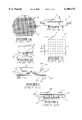
- FIG. 1Ais a plan view of a prior art bumped semiconductor wafer
- FIG. 1Bis an enlarged side elevation view of a bumped die which has been separated from the wafer
- FIG. 1Cis a bottom view of the die taken along section line 1C--1C of FIG. 1B;
- FIG. 1Dis an enlarged cross sectional view taken along section line 1D--1D of FIG. 1B showing a ball bonded to a bonding site on the die;
- FIG. 2is an enlarged cross sectional view of a prior art chip scale package having balls
- FIG. 3is an enlarged cross sectional view of another prior art chip scale package having balls on a separate substrate
- FIG. 4Ais a plan view of a ball retaining plate constructed in accordance with the invention.
- FIG. 4Bis a side elevation view of the ball retaining plate of FIG. 4A;
- FIG. 5Ais an enlarged cross sectional view taken along section line 5A--5A of FIG. 4A illustrating a ball retaining cavity of the ball retaining plate;
- FIG. 5Bis an enlarged cross sectional view illustrating the ball retaining cavity retaining a ball
- FIG. 6Ais a plan view of a substrate alignment member configured to align a substrate, such as a die or chip scale package, with the ball retaining plate;
- FIG. 6Bis a cross sectional view of the substrate alignment member taken along section line 6B--6B of FIG. 6A;
- FIG. 7is a plan view of an alternate embodiment ball retaining plate configured to align and attach balls to a substrate, such as a wafer;
- FIG. 8Ais a plan view of a substrate alignment member configured to align the wafer to the ball retaining plate of FIG. 7;
- FIG. 8Bis a cross sectional view of the substrate alignment member taken along section line 8B--8B of FIG. 8A;
- FIG. 9is a plan view of an alternate embodiment ball retaining plate configured to align and attach balls to multiple substrates at a same time;
- FIG. 10Ais a plan view of an alternate embodiment substrate alignment member configured to align multiple substrates to the ball retaining plate of FIG. 9;
- FIG. 10Bis a cross sectional view taken along section line 10B--10B of FIG. 10A;
- FIG. 11Ais a schematic cross sectional view of the ball retaining plate and the substrate alignment member
- FIG. 11Bis a schematic cross sectional view of a ball loader mechanism and vacuum fixture attached to the ball retaining plate and the substrate alignment member;
- FIG. 11Cis a schematic cross sectional view of the ball retaining plate and the substrate alignment member with balls loaded into the ball retaining cavities;
- FIG. 11Dis a schematic cross sectional view illustrating a substrate on the substrate alignment member having bonding sites in physical contact with balls on the ball retaining plate;
- FIG. 11Eis a schematic cross sectional view of the assembly of FIG. 9 placed in a furnace during reflow and bonding of the balls to the substrate;
- FIG. 12is a schematic view of the furnace
- FIGS. 13A-13Dare schematic cross sectional views illustrating steps in a method for fabricating the ball retaining plate
- FIG. 14Ais a cross sectional view taken along section line 14A of FIG. 13B illustrating a laser machined vacuum conduit in the ball retaining plate;
- FIG. 14Bis a cross sectional view taken along section line 14B of FIG. 13C illustrating the laser machined vacuum conduit following etching
- FIGS. 15A-15Dare schematic cross sectional views illustrating steps in a method for fabricating the substrate alignment member.
- FIGS 1A-1D, 2, and 3various prior art semiconductor substrates having external balls 10 are illustrated.
- the method of the inventionwhich will be hereinafter described, can be used to attach the balls 10 to the substrate.
- the substrateis a semiconductor wafer 12 comprising a plurality of semiconductor dice 14.
- FIG. 1Billustrates a die 14 that has been separated from the wafer 12.
- Each die 14includes a plurality of balls 10 which can be attached to the die 14 using the method of the invention.
- the method of the inventioncan be performed on the wafer 12 prior to singulation of the individual dice 14. Alternately the method of the invention can be performed on singulated dice 14.
- the balls 10are formed on the die 14 in a pattern P1.
- the pattern P1is a dense grid array, such as a ball grid array (BGA).
- BGAball grid array
- a representative diameter D1 for the balls 10can be about 0.005-in (0.127 mm) to 0.050-in (1.270 mm) or greater.
- a representative pitch P (center to center spacing) of the balls 10can be from about 0.008-in (0.228 mm) to about 0.060-in (1.524 mm) or greater.
- the die 14can be provided with a plurality of bonding sites 16.
- FIG. 1Dillustrates one example for a bonding site 16 in the form of a thin film aluminum bond pad embedded in a passivation layer 20.
- FIG. 1Dalso illustrates a single ball 10 that has been bonded to the bonding site 16 on the die 14 using a solder flux 18.
- FIG. 2illustrates another prior art substrate in the form of a chip scale package 22.
- the chip scale package 22includes a silicon body 24 having a recess 26 wherein a semiconductor die 14A is held by an encapsulant 28.
- the package 22also includes conductors 30 wire bonded to the die 14A.
- the conductors 30include bonding sites 16A for the balls 10. Further details of the chip scale package 22 are described in U.S. Pat. No. 5,674,785 to Akram et al. entitled “Method Of Producing A Single Piece Package For Semiconductor Die", and in U.S. Pat. No. 5,739,585, entitled “Single Piece Package For Semiconductor Die", both of which are incorporated herein by reference.
- FIG. 3illustrates another prior art substrate in the form of a chip scale package 32.
- the chip scale package 32includes a die 14B and a BGA substrate 34.
- the BGA substrate 34includes balls 10 in electrical communication with internal conductors 36 in the substrate 34.
- an adhesive layer 40attaches the BGA substrate 34 to the die 14B, with the internal conductors 36 on the BGA substrate 34 in electrical communication with bumps 38 on the die 14B.
- the BGA substrate 34can be formed separately, and the balls 10 attached using the method of the invention prior to attachment of the die 14B. Alternately the balls 10 can be attached to the BGA substrate 34 after attachment of the die 14B.
- a ball retaining plate 42constructed in accordance with the invention is illustrated.
- the ball retaining plate 42is configured to align and attach balls 10 to the singulated die 14.
- a ball retaining plate 42W(FIG. 7) can be configured to align and attach balls 10 to the wafer 12 (FIG. 1A).
- a ball retaining plate 42CSP(FIG. 9) can be configured to align and attach balls 10 to multiple chip scale packages 22 (FIG. 2) at the same time.
- the ball retaining plate 42includes a plurality of ball retaining cavities 44.
- the ball retaining plate 42also includes a plurality of vacuum conduits 46 in flow communication with the ball retaining cavities 44.
- the ball retaining cavities 44are formed on the ball retaining plate 42 in a pattern P2 that matches the pattern P1 (FIG. 1C) of the bonding sites 16 on the die 14.
- a peripheral outline of the ball retaining plate 42matches, but is slightly larger than, a peripheral outline of the die 14.
- each ball retaining cavity 44has sloped sidewalls which can be formed using an anisotropic etch process. The sloped sidewalls help to guide the balls 10 into the ball retaining cavities 44.
- a diameter D2 of each ball retaining cavity 44is approximately equal to, but slightly greater than the diameter D1 of the balls 10 (e.g., D2 is from one to several mils greater than D1).
- a depth D of each ball retaining cavity 44is preferably less than the diameter D1 of the balls 10 (e.g., D is from about 25% to 75% of D1).
- the balls 10can be retained in the cavities 44 while projecting from a surface 48 of the ball retaining plate 42.
- a substrate alignment member 50configured to align the die 14 to the ball retaining plate 42 is illustrated.
- the substrate alignment member 50is fabricated separately and then attached to the ball retaining plate 42.
- the substrate alignment member 50comprises a same material as the ball retaining plate 42 (e.g., silicon, ceramic photosensitive glass).
- the substrate alignment member 50can comprise a polymer material which is deposited on the ball retaining plate 42.
- the substrate alignment member 50includes an alignment opening 52 configured to engage the peripheral edges of the die 14.
- the alignment opening 52includes sloped sidewalls which can be formed using an anisotropic etch process to be hereinafter described. The sloped sidewalls of the alignment opening 52 help to guide and center the die 14 on the ball retaining plate 42.
- an alternate embodiment ball retaining plate 42Wis configured to align and attach balls 10 to the wafer 12.
- the ball retaining plate 42Wincludes a plurality of separate patterns of ball retaining cavities 44 corresponding to the bonding sites 16 (FIG. 1D) on the dice 14 contained on the wafer 12.
- FIGS. 8A and 8Billustrate an alternate embodiment substrate alignment member 50W configured to align the wafer 12 to the ball retaining plate 42W (FIG. 7).
- the substrate alignment member 50Wincludes an alignment opening 52W having a peripheral outline corresponding to the wafer 12. As before, the sidewalls of the alignment opening 52W can be sloped using an anisotropic etch process to be hereinafter described.
- an alternate embodiment ball retaining plate 42CSPis configured to align and attach balls 10 to multiple chip scale packages 22 (or other similarly shaped substrates).
- the ball retaining plate 42CSPincludes a plurality of separate patterns of ball retaining cavities 44 corresponding to the patterns of bonding sites 16 on nine separate chip scale packages 22.
- the nine patterns of ball retaining cavities 44are merely exemplary, as any number of cavities from one or more can be employed.
- FIGS. 10A and 10Billustrate an alternate embodiment substrate alignment member 50CSP configured to align nine separate chip scale packages 22 to the ball retaining plate 42CSP (FIG. 9).
- the substrate alignment member 50CSPincludes nine alignment openings 52CSP having peripheral outlines corresponding to the chip scale packages 22. As before, the sidewalls of the alignment openings 52CSP can be sloped using an anisotropic etch process to be hereinafter described.
- the ball retaining plate 42 and substrate alignment member 50are provided.
- the ball retaining plate 42includes the ball retaining cavities 44 and the vacuum conduits 46.
- the substrate alignment member 50includes an alignment opening 52.
- the substrate alignment member 50has been attached to the ball retaining plate 42, using an adhesive, such as silicone.
- the ball retaining plate 42 and the substrate alignment member 50preferably comprise a same material so that thermal expansion with temperature changes is the same. Also, if the ball retaining plate 42 and the substrate alignment member 50 both comprise silicon, a coefficient of thermal expansion (CTE) of the assembly will exactly match a CTE of a silicon substrate.
- CTEcoefficient of thermal expansion
- a ball loader mechanism 56is attached to the substrate alignment member 50, and a vacuum fixture 62 is attached to the ball retaining plate 42.
- the ball loader mechanism 56includes a reservoir 70 containing a supply of balls 10.
- the ball loader mechanism 56includes a squeegee 60 configured to press balls 10 from the reservoir 70 through openings 54 in a screen 58 onto the ball retaining plate 42.
- the vacuum fixture 62is configured to apply a vacuum through the vacuum conduits 46 to the ball retaining cavities 44.
- the vacuum fixture 62includes a valve 66 and a connector 68 configured for connection to a vacuum source 72.
- the vacuum fixture 62includes a sealed bladder 64 that permits the vacuum to be preserved without the vacuum source 72, once the balls 10 have been seated in the ball retaining cavities 44.
- the balls 10can be pressed by the squeegee 60 through the screen 58 into the ball retaining cavities 44. During this process, a vacuum can be generated in the vacuum conduits 46 for attracting and maintaining the balls 10 in the ball retaining cavities 44.
- FIG. 11Cillustrates the balls 10 seated within the ball retaining cavities 44 and the ball loader mechanism 56 removed. Excess balls 10 can also be removed from the ball retaining plate 42 using a brush or other suitable tool. In addition, the connector 68 can be disconnected from the vacuum source 72, and the valve 66 closed to preserve the vacuum within the bladder 64.
- the die 14can be placed in the alignment opening 52 of the substrate alignment member 50.
- a pick and place mechanism, or a vacuum tool,can be used to place the die 14 in the alignment opening 52.
- the alignment opening 52aligns the die 14, such that the bonding sites 16 on the die 14 align with and physically contact the balls 10 held in the ball retaining cavities 44.
- the vacuum fixture 62can be removed and an assembly 76 comprising the die 14, the substrate alignment member 50 and the ball retaining plate 42 can be placed in a furnace 74.
- the vacuum fixture 62can remain attached to the ball retaining plate 42 and the vacuum preserved during placement of the assembly 76 in the furnace 74.
- the furnace 74includes a conveyor 80 for moving the assemblies 76 through the furnace 74 at a desired speed.
- the furnace 74includes a heat source 82 for heating the balls 10 and bonding sites 16 to a temperature that is above the melting point of the balls 10. This reflows and bonds the balls 10 to the bonding sites 16.
- the bonding sites 16can include a non-oxidizing solder wettable layer, such as gold, platinum or palladium, which will facilitate the bonding process.
- the melting point of the balls 10will be dependent on the solder. Suitable solder alloys include 95%Pb/5%Sn, 60%Pb/40%Sn, 63%Sn/37%Pb, or 62%Pb/36%Sn/2%Ag. Depending on their composition these Pb/Sn solders will have a melting point of from about 150° C. to about 200° C.
- the balls 10can comprise a relatively hard wear resistant metal such as nickel, copper, beryllium copper, alloys of nickel, alloys of copper, alloys of beryllium copper, nickel-cobalt-iron alloys, and iron-nickel alloys.
- a relatively hard wear resistant metalsuch as nickel, copper, beryllium copper, alloys of nickel, alloys of copper, alloys of beryllium copper, nickel-cobalt-iron alloys, and iron-nickel alloys.
- these metalsare limited to applications wherein the high temperatures required to reflow the balls 10 will not be detrimental to integrated circuits and electrical elements contained on the substrate.
- the BGA substrate 34(FIG. 3) does not include integrated circuits, and could be heated to temperatures high enough to reflow balls 10 formed of the above metals.
- solder fluxcan be applied to either the balls 10 or to the bonding sites 16.
- heatingcan be to a temperature high enough to melt the solder flux.
- the solder fluxthen bonds the balls 10 to the bonding sites 16.
- Layers of solder fluxcan be applied to the balls 10 or to the bonding sites 16 by screen printing or other suitable deposition process.
- the furnace 74can include a sealed process chamber 88 in flow communication with a vacuum pump 84, and an inert gas supply 86. Such an arrangement can be used to purge the chamber 88 of oxygen, which inhibits formation of oxide layers, and facilitates formation of a bond between the balls 10 and bonding sites 16.
- a representative vacuum pressure in the process chamber 88can be from about 10 -1 to 10 -3 torr.
- This type of furnace 74 with a sealed process chamber 88is commercially available from Scientific Sealing Technology (SST) of Downey, Calif.
- a wafer blank 90can be provided. Suitable materials for the wafer blank 90 include monocrystalline silicon, ceramic, photosensitive glass and gallium arsenide. A representative thickness for the wafer blank 90 can be from 0.012-in (0.305 mm) to 0.120-in (3.05 mm) or greater.
- the wafer blank 90can be large enough to fabricate a plurality of ball retaining plates 42 using a wafer level fabrication process. For simplicity in FIGS. 13A-13D, only a single ball retaining plate 42 is illustrated. Also, the fabrication steps for the alternate embodiment ball retaining plates 42W (FIG. 7) and 42CSP (FIG. 9) will be substantially the same as illustrated in FIGS. 13A-13D for ball retaining plate 42.
- the vacuum conduits 46can be formed in the wafer blank 90 using a suitable process.
- One method for forming the vacuum conduits 46is with a laser machining process.
- a suitable laser machining apparatusis manufactured by General Scanning of Sommerville, Mass. and is designated a model no. 670-W.
- a representative diameter of the vacuum conduits 46can be from 10 ⁇ m to 2 mils or greater.
- a representative laser fluence for forming the vacuum conduits 46 through a wafer blank 90 comprising silicon and having a thickness of about 0.028-in (0.711 mm)is from 2 to 10 watts/per opening at a pulse duration of 20-25 ns and at a repetition rate of up to several thousand per second.
- the wavelength of the laser beamcan be a standard infrared or green wavelength (e.g., 1064 nm-532 nm).
- an etch mask 92can be formed on the wafer blank 90 and used to etch the ball retaining cavities 44.
- the etch mask 92can comprise resist, or a hard mask such as Si 3 N 4 .
- a wet etchantcan be used to anisotropically etch the wafer blank 90 to form the ball retaining cavities 44. If an anisotropic etch procedure is employed, the ball retaining cavities 44 will form as pockets with sloped sidewalls and a decreasing radius. The etched shape of the ball retaining cavities 44 aids in loading the balls 10 into the cavities 44 and in retaining the balls 10 following loading. Such an anisotropic wet etch procedure is sometimes referred to in the art as bulk micro machining.
- a suitable wet etchantcomprises potassium hydroxide (KOH), or alternately a solution of tetra-methyl ammonium hydroxide (TMAH).
- KOHpotassium hydroxide
- TMAHtetra-methyl ammonium hydroxide
- a suitable wet etchantcomprises a solution of HF.
- An ion milling processcan also be used to etch a wafer blank 90 comprising a ceramic material.
- a suitable wet etchantcomprises bromine in methanol (Br 2 --CH 3 OH).
- a suitable wet etchantcomprises HF.
- photosensitive glasses and etchantsare commercially available from Dow Corning under the trademark "FOTOFORM".
- the diameter D2 (FIG. 5A) and depth D (FIG. 5A) of the ball retaining cavities 44will be dependent on the size of etch openings 94 in the etch mask 92 and on the etch parameters.
- the previously machined vacuum conduits 46can also be etched.
- vacuum conduits 46 formed by laser machiningwill initially be circular in cross section.
- FIG. 14Bfollowing an anisotropic wet etch with a silicon wafer blank 90, the vacuum conduits will have a multi faceted cross section (e.g., six sided).
- the etch mask 92can be stripped using a suitable wet chemical.
- a suitable wet chemicalfor stripping the mask 92 comprises H 3 PO 4 .
- the substrate alignment member 50can be attached to the ball retaining plate 42.
- One method of attachmentis by forming an adhesive layer 96 out of silicone or other polymeric material.
- a deposited polymercan be used to form the substrate alignment member 50 directly on the ball retaining plate 42.
- One suitable polymercomprises a thick film resist sold by Shell Chemical under the trademark "EPON RESIN SU-8".
- the resistincludes an organic solvent (e.g., gamma-butyloracton), and a photoinitiator.
- a conventional resist coating apparatussuch as a spin coater, or a meniscus coater, along with a mask or stencil, can be used to deposit the resist in viscous form onto the ball retaining plate 42.
- the deposited resistcan then be partially hardened by heating to about 95° C. for about 15 minutes or longer. Following partial hardening, the resist can be developed and etched to form the alignment opening 52, and then fully hardened by heating to about 95° C. for about an hour.
- FIGS. 15A-15Dsteps in a method for fabricating the substrate alignment member 50 are illustrated. Initially, as shown in FIG. 15A, a wafer blank 98 can be provided as previously described for wafer blank 90 (FIG. 13A).
- an etch mask 100 with an etch opening 102can be formed on the wafer blank 98.
- the etch mask 100can be formed as previously described for etch mask 92 (FIG. 13C).
- the alignment opening 52can be formed using a wet etch process as previously described for the ball retaining cavities 44 (FIG. 13C).
- the etch mask 100can be stripped as previously described for etch mask 92.
Landscapes
- Engineering & Computer Science (AREA)
- Manufacturing & Machinery (AREA)
- Microelectronics & Electronic Packaging (AREA)
- Computer Hardware Design (AREA)
- Power Engineering (AREA)
- Ceramic Engineering (AREA)
- Physics & Mathematics (AREA)
- Condensed Matter Physics & Semiconductors (AREA)
- General Physics & Mathematics (AREA)
- Micromachines (AREA)
- Wire Bonding (AREA)
Abstract
Description
Claims (10)
Priority Applications (2)
| Application Number | Priority Date | Filing Date | Title |
|---|---|---|---|
| US09/143,631US6100175A (en) | 1998-08-28 | 1998-08-28 | Method and apparatus for aligning and attaching balls to a substrate |
| US09/519,583US6364196B1 (en) | 1998-08-28 | 2000-03-06 | Method and apparatus for aligning and attaching balls to a substrate |
Applications Claiming Priority (1)
| Application Number | Priority Date | Filing Date | Title |
|---|---|---|---|
| US09/143,631US6100175A (en) | 1998-08-28 | 1998-08-28 | Method and apparatus for aligning and attaching balls to a substrate |
Related Child Applications (1)
| Application Number | Title | Priority Date | Filing Date |
|---|---|---|---|
| US09/519,583DivisionUS6364196B1 (en) | 1998-08-28 | 2000-03-06 | Method and apparatus for aligning and attaching balls to a substrate |
Publications (1)
| Publication Number | Publication Date |
|---|---|
| US6100175Atrue US6100175A (en) | 2000-08-08 |
Family
ID=22504909
Family Applications (2)
| Application Number | Title | Priority Date | Filing Date |
|---|---|---|---|
| US09/143,631Expired - LifetimeUS6100175A (en) | 1998-08-28 | 1998-08-28 | Method and apparatus for aligning and attaching balls to a substrate |
| US09/519,583Expired - Fee RelatedUS6364196B1 (en) | 1998-08-28 | 2000-03-06 | Method and apparatus for aligning and attaching balls to a substrate |
Family Applications After (1)
| Application Number | Title | Priority Date | Filing Date |
|---|---|---|---|
| US09/519,583Expired - Fee RelatedUS6364196B1 (en) | 1998-08-28 | 2000-03-06 | Method and apparatus for aligning and attaching balls to a substrate |
Country Status (1)
| Country | Link |
|---|---|
| US (2) | US6100175A (en) |
Cited By (18)
| Publication number | Priority date | Publication date | Assignee | Title |
|---|---|---|---|---|
| US6186389B1 (en)* | 1999-04-30 | 2001-02-13 | Shinko Electric Industries Co., Ltd. | Apparatus and process for mounting conductor balls on terminal pads of semiconductor devices |
| US6186392B1 (en) | 2000-01-21 | 2001-02-13 | Micron Technology, Inc. | Method and system for forming contacts on a semiconductor component by aligning and attaching ferromagnetic balls |
| US6284568B1 (en)* | 1998-07-31 | 2001-09-04 | Kabushiki Kaisha Toshiba | Method and system for producing semiconductor device |
| US6364196B1 (en) | 1998-08-28 | 2002-04-02 | Micron Technology, Inc. | Method and apparatus for aligning and attaching balls to a substrate |
| US6600171B1 (en) | 2001-04-02 | 2003-07-29 | Micron Technology, Inc. | Semiconductor component and system for fabricating contacts on semiconductor components |
| US6854633B1 (en) | 2002-02-05 | 2005-02-15 | Micron Technology, Inc. | System with polymer masking flux for fabricating external contacts on semiconductor components |
| US20050208703A1 (en)* | 1999-06-17 | 2005-09-22 | Infineon Technologies, Ag | Method of producing an electronic component with flexible bonding pads |
| US20060261446A1 (en)* | 2005-05-19 | 2006-11-23 | Micron Technology, Inc. | Backside method and system for fabricating semiconductor components with conductive interconnects |
| US20060261402A1 (en)* | 2005-05-20 | 2006-11-23 | Hang-Ting Lue | Air tunnel floating gate memory cell and method for making the same |
| US20060289992A1 (en)* | 2005-06-27 | 2006-12-28 | Micron Technology, Inc. | Stacked semiconductor component, fabrication method and fabrication system |
| US20070202617A1 (en)* | 2005-04-08 | 2007-08-30 | Hembree David R | Method for fabricating stacked semiconductor components with through wire interconnects |
| US20080042247A1 (en)* | 2005-12-07 | 2008-02-21 | Wood Alan G | Stacked Semiconductor Components With Through Wire Interconnects (TWI) |
| US7659612B2 (en) | 2006-04-24 | 2010-02-09 | Micron Technology, Inc. | Semiconductor components having encapsulated through wire interconnects (TWI) |
| US20130149858A1 (en)* | 2011-12-12 | 2013-06-13 | Samsung Electronics Co., Ltd. | Method of manufacturing bump |
| US20170168251A1 (en)* | 2014-07-31 | 2017-06-15 | Hewlett Packard Enterprise Development Lp | Interposer registration elements |
| US20190001425A1 (en)* | 2016-09-21 | 2019-01-03 | Origin Electric Company, Limited | Heating apparatus and method for producing plate-like object |
| US11541610B2 (en)* | 2019-04-01 | 2023-01-03 | Huber+Suhner Polatls Limited | Method and apparatus for suction alignment |
| TWI842168B (en)* | 2021-10-29 | 2024-05-11 | 李元福 | Pressing system for pressing balls onto strip for bga package |
Families Citing this family (10)
| Publication number | Priority date | Publication date | Assignee | Title |
|---|---|---|---|---|
| TW451359B (en)* | 1999-03-16 | 2001-08-21 | Matsushita Electric Industrial Co Ltd | Mounting equipment and mounting method of conductive balls |
| US7394153B2 (en)* | 1999-12-17 | 2008-07-01 | Osram Opto Semiconductors Gmbh | Encapsulation of electronic devices |
| WO2001045140A2 (en)* | 1999-12-17 | 2001-06-21 | Osram Opto Semiconductors Gmbh | Encapsulation for organic led device |
| US6762502B1 (en)* | 2000-08-31 | 2004-07-13 | Micron Technology, Inc. | Semiconductor device packages including a plurality of layers substantially encapsulating leads thereof |
| US6739498B2 (en)* | 2001-05-17 | 2004-05-25 | Intel Corporation | Solder ball attachment system |
| US6921860B2 (en) | 2003-03-18 | 2005-07-26 | Micron Technology, Inc. | Microelectronic component assemblies having exposed contacts |
| EP1675168A2 (en)* | 2004-12-21 | 2006-06-28 | St Microelectronics S.A. | Process and device for the positioning of connection balls for integrated circuits |
| WO2007019732A1 (en) | 2005-08-19 | 2007-02-22 | Intel Corporation | Surface mount component having magnetic layer thereon and method of forming same |
| US9538582B2 (en) | 2012-07-26 | 2017-01-03 | Taiwan Semiconductor Manufacturing Company, Ltd. | Warpage control in the packaging of integrated circuits |
| CN105215601B (en)* | 2015-10-22 | 2017-02-08 | 海门市彼维知识产权服务有限公司 | Multifunctional safe welding jig for bimorph and copper wire |
Citations (14)
| Publication number | Priority date | Publication date | Assignee | Title |
|---|---|---|---|---|
| US4830264A (en)* | 1986-10-08 | 1989-05-16 | International Business Machines Corporation | Method of forming solder terminals for a pinless ceramic module |
| US5118027A (en)* | 1991-04-24 | 1992-06-02 | International Business Machines Corporation | Method of aligning and mounting solder balls to a substrate |
| US5299730A (en)* | 1989-08-28 | 1994-04-05 | Lsi Logic Corporation | Method and apparatus for isolation of flux materials in flip-chip manufacturing |
| US5446960A (en)* | 1994-02-15 | 1995-09-05 | International Business Machines Corporation | Alignment apparatus and method for placing modules on a circuit board |
| US5620927A (en)* | 1995-05-25 | 1997-04-15 | National Semiconductor Corporation | Solder ball attachment machine for semiconductor packages |
| US5643831A (en)* | 1994-01-20 | 1997-07-01 | Fujitsu Limited | Process for forming solder balls on a plate having apertures using solder paste and transferring the solder balls to semiconductor device |
| US5646095A (en)* | 1991-06-18 | 1997-07-08 | International Business Machines Corporation | Selective insulation etching for fabricating superconductor microcircuits |
| US5674785A (en)* | 1995-11-27 | 1997-10-07 | Micron Technology, Inc. | Method of producing a single piece package for semiconductor die |
| US5679267A (en)* | 1994-04-04 | 1997-10-21 | Texas Instruments Incorporated | Dual etching of ceramic materials with an elevated thin film |
| US5841198A (en)* | 1997-04-21 | 1998-11-24 | Lsi Logic Corporation | Ball grid array package employing solid core solder balls |
| US5872400A (en)* | 1997-06-25 | 1999-02-16 | International Business Machines Corporation | High melting point solder ball coated with a low melting point solder |
| US5899737A (en)* | 1996-09-20 | 1999-05-04 | Lsi Logic Corporation | Fluxless solder ball attachment process |
| US5930889A (en)* | 1996-11-05 | 1999-08-03 | Micron Electronics, Inc. | Method for mounting packaged integrated circuit devices to printed circuit boards |
| US5986348A (en)* | 1999-03-15 | 1999-11-16 | Ball Semiconductor Inc. | Magnetic alignment system for bumps on an integrated circuit device |
Family Cites Families (23)
| Publication number | Priority date | Publication date | Assignee | Title |
|---|---|---|---|---|
| JPH0795554B2 (en)* | 1987-09-14 | 1995-10-11 | 株式会社日立製作所 | Solder ball alignment device |
| JP2795788B2 (en) | 1993-02-18 | 1998-09-10 | シャープ株式会社 | Semiconductor chip mounting method |
| US5346775A (en) | 1993-02-22 | 1994-09-13 | At&T Laboratories | Article comprising solder with improved mechanical properties |
| US5539153A (en) | 1994-08-08 | 1996-07-23 | Hewlett-Packard Company | Method of bumping substrates by contained paste deposition |
| JPH08162455A (en)* | 1994-12-06 | 1996-06-21 | Toshiba Corp | Spherical electrode forming method and forming apparatus |
| US5620129A (en)* | 1995-02-17 | 1997-04-15 | Rogren; Philip E. | Device and method for forming and attaching an array of conductive balls |
| US5839641A (en)* | 1995-08-30 | 1998-11-24 | Industrial Technology Research Institute | Apparatus for placing and aligning solder balls onto solder pads on a substrate for manufacturing IC devices |
| US5687901A (en)* | 1995-11-14 | 1997-11-18 | Nippon Steel Corporation | Process and apparatus for forming ball bumps |
| US5816482A (en) | 1996-04-26 | 1998-10-06 | The Whitaker Corporation | Method and apparatus for attaching balls to a substrate |
| US5762258A (en)* | 1996-07-23 | 1998-06-09 | International Business Machines Corporation | Method of making an electronic package having spacer elements |
| US5801452A (en) | 1996-10-25 | 1998-09-01 | Micron Technology, Inc. | Multi chip module including semiconductor wafer or dice, interconnect substrate, and alignment member |
| US6119927A (en)* | 1997-02-18 | 2000-09-19 | Edm Supplies, Inc. | Method and apparatus for placing and attaching solder balls to substrates |
| US5918792A (en)* | 1997-04-04 | 1999-07-06 | Rvsi Vanguard, Inc. | Apparatus and method for filling a ball grid array |
| JP2850901B2 (en)* | 1997-06-02 | 1999-01-27 | 日本電気株式会社 | Ball arrangement jig and manufacturing method thereof |
| US6040702A (en) | 1997-07-03 | 2000-03-21 | Micron Technology, Inc. | Carrier and system for testing bumped semiconductor components |
| US6107122A (en) | 1997-08-04 | 2000-08-22 | Micron Technology, Inc. | Direct die contact (DDC) semiconductor package |
| US6072326A (en) | 1997-08-22 | 2000-06-06 | Micron Technology, Inc. | System for testing semiconductor components |
| US6018249A (en) | 1997-12-11 | 2000-01-25 | Micron Technolgoy, Inc. | Test system with mechanical alignment for semiconductor chip scale packages and dice |
| US6107109A (en) | 1997-12-18 | 2000-08-22 | Micron Technology, Inc. | Method for fabricating a semiconductor interconnect with laser machined electrical paths through substrate |
| US6114240A (en) | 1997-12-18 | 2000-09-05 | Micron Technology, Inc. | Method for fabricating semiconductor components using focused laser beam |
| US6100175A (en) | 1998-08-28 | 2000-08-08 | Micron Technology, Inc. | Method and apparatus for aligning and attaching balls to a substrate |
| US6118179A (en) | 1999-08-27 | 2000-09-12 | Micron Technology, Inc. | Semiconductor component with external contact polymer support member and method of fabrication |
| US6186392B1 (en) | 2000-01-21 | 2001-02-13 | Micron Technology, Inc. | Method and system for forming contacts on a semiconductor component by aligning and attaching ferromagnetic balls |
- 1998
- 1998-08-28USUS09/143,631patent/US6100175A/ennot_activeExpired - Lifetime
- 2000
- 2000-03-06USUS09/519,583patent/US6364196B1/ennot_activeExpired - Fee Related
Patent Citations (15)
| Publication number | Priority date | Publication date | Assignee | Title |
|---|---|---|---|---|
| US4830264A (en)* | 1986-10-08 | 1989-05-16 | International Business Machines Corporation | Method of forming solder terminals for a pinless ceramic module |
| US5299730A (en)* | 1989-08-28 | 1994-04-05 | Lsi Logic Corporation | Method and apparatus for isolation of flux materials in flip-chip manufacturing |
| US5118027A (en)* | 1991-04-24 | 1992-06-02 | International Business Machines Corporation | Method of aligning and mounting solder balls to a substrate |
| US5646095A (en)* | 1991-06-18 | 1997-07-08 | International Business Machines Corporation | Selective insulation etching for fabricating superconductor microcircuits |
| US5643831A (en)* | 1994-01-20 | 1997-07-01 | Fujitsu Limited | Process for forming solder balls on a plate having apertures using solder paste and transferring the solder balls to semiconductor device |
| US5446960A (en)* | 1994-02-15 | 1995-09-05 | International Business Machines Corporation | Alignment apparatus and method for placing modules on a circuit board |
| US5679267A (en)* | 1994-04-04 | 1997-10-21 | Texas Instruments Incorporated | Dual etching of ceramic materials with an elevated thin film |
| US5620927A (en)* | 1995-05-25 | 1997-04-15 | National Semiconductor Corporation | Solder ball attachment machine for semiconductor packages |
| US5674785A (en)* | 1995-11-27 | 1997-10-07 | Micron Technology, Inc. | Method of producing a single piece package for semiconductor die |
| US5739585A (en)* | 1995-11-27 | 1998-04-14 | Micron Technology, Inc. | Single piece package for semiconductor die |
| US5899737A (en)* | 1996-09-20 | 1999-05-04 | Lsi Logic Corporation | Fluxless solder ball attachment process |
| US5930889A (en)* | 1996-11-05 | 1999-08-03 | Micron Electronics, Inc. | Method for mounting packaged integrated circuit devices to printed circuit boards |
| US5841198A (en)* | 1997-04-21 | 1998-11-24 | Lsi Logic Corporation | Ball grid array package employing solid core solder balls |
| US5872400A (en)* | 1997-06-25 | 1999-02-16 | International Business Machines Corporation | High melting point solder ball coated with a low melting point solder |
| US5986348A (en)* | 1999-03-15 | 1999-11-16 | Ball Semiconductor Inc. | Magnetic alignment system for bumps on an integrated circuit device |
Non-Patent Citations (2)
| Title |
|---|
| Studt, Tim, "Vacuum Process Cuts BGA Rework", R & D Magazine, May 1997, pp. 75-77. |
| Studt, Tim, Vacuum Process Cuts BGA Rework , R & D Magazine, May 1997, pp. 75 77.* |
Cited By (56)
| Publication number | Priority date | Publication date | Assignee | Title |
|---|---|---|---|---|
| US6284568B1 (en)* | 1998-07-31 | 2001-09-04 | Kabushiki Kaisha Toshiba | Method and system for producing semiconductor device |
| US6364196B1 (en) | 1998-08-28 | 2002-04-02 | Micron Technology, Inc. | Method and apparatus for aligning and attaching balls to a substrate |
| US6186389B1 (en)* | 1999-04-30 | 2001-02-13 | Shinko Electric Industries Co., Ltd. | Apparatus and process for mounting conductor balls on terminal pads of semiconductor devices |
| US20050208703A1 (en)* | 1999-06-17 | 2005-09-22 | Infineon Technologies, Ag | Method of producing an electronic component with flexible bonding pads |
| US7820482B2 (en)* | 1999-06-17 | 2010-10-26 | Qimonda Ag | Method of producing an electronic component with flexible bonding |
| US6186392B1 (en) | 2000-01-21 | 2001-02-13 | Micron Technology, Inc. | Method and system for forming contacts on a semiconductor component by aligning and attaching ferromagnetic balls |
| US6283358B1 (en) | 2000-01-21 | 2001-09-04 | Micron Technology, Inc. | System for forming contacts on a semiconductor component by aligning and attaching ferromagnetic balls |
| US6600171B1 (en) | 2001-04-02 | 2003-07-29 | Micron Technology, Inc. | Semiconductor component and system for fabricating contacts on semiconductor components |
| US6680213B2 (en) | 2001-04-02 | 2004-01-20 | Micron Technology, Inc. | Method and system for fabricating contacts on semiconductor components |
| US6854633B1 (en) | 2002-02-05 | 2005-02-15 | Micron Technology, Inc. | System with polymer masking flux for fabricating external contacts on semiconductor components |
| US6926191B2 (en) | 2002-02-05 | 2005-08-09 | Micron Technology, Inc. | Process for fabricating external contacts on semiconductor components |
| US7757385B2 (en) | 2005-04-08 | 2010-07-20 | Micron Technology, Inc. | System for fabricating semiconductor components with through wire interconnects |
| US7682962B2 (en) | 2005-04-08 | 2010-03-23 | Micron Technology, Inc. | Method for fabricating stacked semiconductor components with through wire interconnects |
| US20070202617A1 (en)* | 2005-04-08 | 2007-08-30 | Hembree David R | Method for fabricating stacked semiconductor components with through wire interconnects |
| US20070200255A1 (en)* | 2005-04-08 | 2007-08-30 | Hembree David R | System for fabricating semiconductor components with through wire interconnects |
| US20070222054A1 (en)* | 2005-04-08 | 2007-09-27 | Hembree David R | Semiconductor components with through wire interconnects |
| US8053909B2 (en) | 2005-04-08 | 2011-11-08 | Micron Technology, Inc. | Semiconductor component having through wire interconnect with compressed bump |
| US7919846B2 (en) | 2005-04-08 | 2011-04-05 | Micron Technology, Inc. | Stacked semiconductor component having through wire interconnect |
| US7728443B2 (en) | 2005-04-08 | 2010-06-01 | Micron Technology, Inc. | Semiconductor components with through wire interconnects |
| US8546931B2 (en) | 2005-05-19 | 2013-10-01 | Micron Technology, Inc. | Stacked semiconductor components having conductive interconnects |
| US7768096B2 (en) | 2005-05-19 | 2010-08-03 | Micron Technology, Inc. | System for fabricating semiconductor components with conductive interconnects |
| US7951702B2 (en) | 2005-05-19 | 2011-05-31 | Micron Technology, Inc. | Methods for fabricating semiconductor components with conductive interconnects having planar surfaces |
| US7935991B2 (en) | 2005-05-19 | 2011-05-03 | Micron Technology, Inc. | Semiconductor components with conductive interconnects |
| US7393770B2 (en) | 2005-05-19 | 2008-07-01 | Micron Technology, Inc. | Backside method for fabricating semiconductor components with conductive interconnects |
| US20060261446A1 (en)* | 2005-05-19 | 2006-11-23 | Micron Technology, Inc. | Backside method and system for fabricating semiconductor components with conductive interconnects |
| US20080229573A1 (en)* | 2005-05-19 | 2008-09-25 | Wood Alan G | System For Fabricating Semiconductor Components With Conductive Interconnects |
| US7727872B2 (en) | 2005-05-19 | 2010-06-01 | Micron Technology, Inc. | Methods for fabricating semiconductor components with conductive interconnects |
| US20080206990A1 (en)* | 2005-05-19 | 2008-08-28 | Wood Alan G | Methods For Fabricating Semiconductor Components With Conductive Interconnects |
| US20100144139A1 (en)* | 2005-05-19 | 2010-06-10 | Wood Alan G | Methods For Fabricating Semiconductor Components With Conductive Interconnects Having Planar Surfaces |
| US20060261402A1 (en)* | 2005-05-20 | 2006-11-23 | Hang-Ting Lue | Air tunnel floating gate memory cell and method for making the same |
| US8258006B2 (en) | 2005-06-27 | 2012-09-04 | Micron Technology, Inc. | Method for fabricating stacked semiconductor components |
| US20060289992A1 (en)* | 2005-06-27 | 2006-12-28 | Micron Technology, Inc. | Stacked semiconductor component, fabrication method and fabrication system |
| US7589406B2 (en) | 2005-06-27 | 2009-09-15 | Micron Technology, Inc. | Stacked semiconductor component |
| US20090068791A1 (en)* | 2005-06-27 | 2009-03-12 | Wood Alan G | Method For Fabricating Stacked Semiconductor Components |
| US7786605B2 (en) | 2005-12-07 | 2010-08-31 | Micron Technology, Inc. | Stacked semiconductor components with through wire interconnects (TWI) |
| US8513797B2 (en) | 2005-12-07 | 2013-08-20 | Micron Technology, Inc. | Stacked semiconductor component having through wire interconnect (TWI) with compressed wire |
| US9013044B2 (en) | 2005-12-07 | 2015-04-21 | Micron Technology, Inc. | Through wire interconnect (TWI) for semiconductor components having wire in via and bonded connection with substrate contact |
| US7579267B2 (en) | 2005-12-07 | 2009-08-25 | Micron Technology, Inc. | Methods and systems for fabricating semiconductor components with through wire interconnects (TWI) |
| US20080042247A1 (en)* | 2005-12-07 | 2008-02-21 | Wood Alan G | Stacked Semiconductor Components With Through Wire Interconnects (TWI) |
| US8193646B2 (en) | 2005-12-07 | 2012-06-05 | Micron Technology, Inc. | Semiconductor component having through wire interconnect (TWI) with compressed wire |
| US8120167B2 (en) | 2006-04-24 | 2012-02-21 | Micron Technology, Inc. | System with semiconductor components having encapsulated through wire interconnects (TWI) |
| US8741667B2 (en) | 2006-04-24 | 2014-06-03 | Micron Technology, Inc. | Method for fabricating a through wire interconnect (TWI) on a semiconductor substrate having a bonded connection and an encapsulating polymer layer |
| US8404523B2 (en) | 2006-04-24 | 2013-03-26 | Micron Technoloy, Inc. | Method for fabricating stacked semiconductor system with encapsulated through wire interconnects (TWI) |
| US9018751B2 (en) | 2006-04-24 | 2015-04-28 | Micron Technology, Inc. | Semiconductor module system having encapsulated through wire interconnect (TWI) |
| US7883908B2 (en) | 2006-04-24 | 2011-02-08 | Micron Technology, Inc. | Method for fabricating semiconductor component having encapsulated through wire interconnect (TWI) |
| US20100047934A1 (en)* | 2006-04-24 | 2010-02-25 | Hembree David R | Method For Fabricating Semiconductor Component Having Encapsulated Through Wire Interconnect (TWI) |
| US8581387B1 (en) | 2006-04-24 | 2013-11-12 | Micron Technology, Inc. | Through wire interconnect (TWI) having bonded connection and encapsulating polymer layer |
| US8217510B2 (en) | 2006-04-24 | 2012-07-10 | Micron Technology, Inc. | Semiconductor module system having stacked components with encapsulated through wire interconnects (TWI) |
| US7659612B2 (en) | 2006-04-24 | 2010-02-09 | Micron Technology, Inc. | Semiconductor components having encapsulated through wire interconnects (TWI) |
| US20130149858A1 (en)* | 2011-12-12 | 2013-06-13 | Samsung Electronics Co., Ltd. | Method of manufacturing bump |
| US9269620B2 (en)* | 2011-12-12 | 2016-02-23 | Samsung Electronics Co., Ltd. | Method of manufacturing bump |
| US20170168251A1 (en)* | 2014-07-31 | 2017-06-15 | Hewlett Packard Enterprise Development Lp | Interposer registration elements |
| US9921377B2 (en)* | 2014-07-31 | 2018-03-20 | Hewlett Packard Enterprise Department LP | Interposer registration elements |
| US20190001425A1 (en)* | 2016-09-21 | 2019-01-03 | Origin Electric Company, Limited | Heating apparatus and method for producing plate-like object |
| US11541610B2 (en)* | 2019-04-01 | 2023-01-03 | Huber+Suhner Polatls Limited | Method and apparatus for suction alignment |
| TWI842168B (en)* | 2021-10-29 | 2024-05-11 | 李元福 | Pressing system for pressing balls onto strip for bga package |
Also Published As
| Publication number | Publication date |
|---|---|
| US6364196B1 (en) | 2002-04-02 |
Similar Documents
| Publication | Publication Date | Title |
|---|---|---|
| US6100175A (en) | Method and apparatus for aligning and attaching balls to a substrate | |
| US6186392B1 (en) | Method and system for forming contacts on a semiconductor component by aligning and attaching ferromagnetic balls | |
| US6861345B2 (en) | Method of disposing conductive bumps onto a semiconductor device | |
| US5607099A (en) | Solder bump transfer device for flip chip integrated circuit devices | |
| KR100257420B1 (en) | Systems interconnected by bumps of joining material | |
| US6107122A (en) | Direct die contact (DDC) semiconductor package | |
| US6832747B2 (en) | Hybrid molds for molten solder screening process | |
| JP3202903B2 (en) | Method of forming solder balls on a substrate | |
| JP3385872B2 (en) | Solder supply method and solder supply apparatus | |
| KR100267874B1 (en) | Method for making interconnect for low temperature chip attachment | |
| US6319810B1 (en) | Method for forming solder bumps | |
| US6723629B2 (en) | Method and apparatus for attaching solder members to a substrate | |
| US6213386B1 (en) | Method of forming bumps | |
| JP4057399B2 (en) | Method for filling metal into fine holes | |
| US5494856A (en) | Apparatus and method for creating detachable solder connections | |
| WO2007076099A2 (en) | Microelectronic elements with compliant terminal mountings and methods for making the same | |
| KR20160108196A (en) | Method for manufacturing semiconductor device | |
| JPH10163213A (en) | Semiconductor device manufacturing method and semiconductor device mounting method | |
| EP1916712A2 (en) | Method for mounting electronic component on substrate and method for forming solder surface | |
| US7211888B2 (en) | Encapsulation of pin solder for maintaining accuracy in pin position | |
| US20060011712A1 (en) | Improved decal solder transfer method | |
| US20080029686A1 (en) | Precision fabricated silicon mold | |
| JP2735038B2 (en) | Bump forming method | |
| US6574861B1 (en) | System and method for solder ball rework | |
| JP2910398B2 (en) | Solder bump formation method |
Legal Events
| Date | Code | Title | Description |
|---|---|---|---|
| AS | Assignment | Owner name:MICRON TECHNOLOGY, INC., IDAHO Free format text:ASSIGNMENT OF ASSIGNORS INTEREST;ASSIGNORS:WOOD, ALAN G.;AKRAM, SALMAN;HESS, MIKE;AND OTHERS;REEL/FRAME:009431/0766;SIGNING DATES FROM 19980820 TO 19980826 | |
| STCF | Information on status: patent grant | Free format text:PATENTED CASE | |
| FEPP | Fee payment procedure | Free format text:PAYOR NUMBER ASSIGNED (ORIGINAL EVENT CODE: ASPN); ENTITY STATUS OF PATENT OWNER: LARGE ENTITY | |
| FPAY | Fee payment | Year of fee payment:4 | |
| FPAY | Fee payment | Year of fee payment:8 | |
| FPAY | Fee payment | Year of fee payment:12 | |
| AS | Assignment | Owner name:U.S. BANK NATIONAL ASSOCIATION, AS COLLATERAL AGENT, CALIFORNIA Free format text:SECURITY INTEREST;ASSIGNOR:MICRON TECHNOLOGY, INC.;REEL/FRAME:038669/0001 Effective date:20160426 Owner name:U.S. BANK NATIONAL ASSOCIATION, AS COLLATERAL AGEN Free format text:SECURITY INTEREST;ASSIGNOR:MICRON TECHNOLOGY, INC.;REEL/FRAME:038669/0001 Effective date:20160426 | |
| AS | Assignment | Owner name:MORGAN STANLEY SENIOR FUNDING, INC., AS COLLATERAL AGENT, MARYLAND Free format text:PATENT SECURITY AGREEMENT;ASSIGNOR:MICRON TECHNOLOGY, INC.;REEL/FRAME:038954/0001 Effective date:20160426 Owner name:MORGAN STANLEY SENIOR FUNDING, INC., AS COLLATERAL Free format text:PATENT SECURITY AGREEMENT;ASSIGNOR:MICRON TECHNOLOGY, INC.;REEL/FRAME:038954/0001 Effective date:20160426 | |
| AS | Assignment | Owner name:U.S. BANK NATIONAL ASSOCIATION, AS COLLATERAL AGENT, CALIFORNIA Free format text:CORRECTIVE ASSIGNMENT TO CORRECT THE REPLACE ERRONEOUSLY FILED PATENT #7358718 WITH THE CORRECT PATENT #7358178 PREVIOUSLY RECORDED ON REEL 038669 FRAME 0001. ASSIGNOR(S) HEREBY CONFIRMS THE SECURITY INTEREST;ASSIGNOR:MICRON TECHNOLOGY, INC.;REEL/FRAME:043079/0001 Effective date:20160426 Owner name:U.S. BANK NATIONAL ASSOCIATION, AS COLLATERAL AGEN Free format text:CORRECTIVE ASSIGNMENT TO CORRECT THE REPLACE ERRONEOUSLY FILED PATENT #7358718 WITH THE CORRECT PATENT #7358178 PREVIOUSLY RECORDED ON REEL 038669 FRAME 0001. ASSIGNOR(S) HEREBY CONFIRMS THE SECURITY INTEREST;ASSIGNOR:MICRON TECHNOLOGY, INC.;REEL/FRAME:043079/0001 Effective date:20160426 | |
| AS | Assignment | Owner name:JPMORGAN CHASE BANK, N.A., AS COLLATERAL AGENT, ILLINOIS Free format text:SECURITY INTEREST;ASSIGNORS:MICRON TECHNOLOGY, INC.;MICRON SEMICONDUCTOR PRODUCTS, INC.;REEL/FRAME:047540/0001 Effective date:20180703 Owner name:JPMORGAN CHASE BANK, N.A., AS COLLATERAL AGENT, IL Free format text:SECURITY INTEREST;ASSIGNORS:MICRON TECHNOLOGY, INC.;MICRON SEMICONDUCTOR PRODUCTS, INC.;REEL/FRAME:047540/0001 Effective date:20180703 | |
| AS | Assignment | Owner name:MICRON TECHNOLOGY, INC., IDAHO Free format text:RELEASE BY SECURED PARTY;ASSIGNOR:U.S. BANK NATIONAL ASSOCIATION, AS COLLATERAL AGENT;REEL/FRAME:047243/0001 Effective date:20180629 | |
| AS | Assignment | Owner name:MICRON TECHNOLOGY, INC., IDAHO Free format text:RELEASE BY SECURED PARTY;ASSIGNOR:MORGAN STANLEY SENIOR FUNDING, INC., AS COLLATERAL AGENT;REEL/FRAME:050937/0001 Effective date:20190731 | |
| AS | Assignment | Owner name:MICRON SEMICONDUCTOR PRODUCTS, INC., IDAHO Free format text:RELEASE BY SECURED PARTY;ASSIGNOR:JPMORGAN CHASE BANK, N.A., AS COLLATERAL AGENT;REEL/FRAME:051028/0001 Effective date:20190731 Owner name:MICRON TECHNOLOGY, INC., IDAHO Free format text:RELEASE BY SECURED PARTY;ASSIGNOR:JPMORGAN CHASE BANK, N.A., AS COLLATERAL AGENT;REEL/FRAME:051028/0001 Effective date:20190731 |