US6099132A - Manufacture method for micromechanical devices - Google Patents
Manufacture method for micromechanical devicesDownload PDFInfo
- Publication number
- US6099132A US6099132AUS08/483,777US48377795AUS6099132AUS 6099132 AUS6099132 AUS 6099132AUS 48377795 AUS48377795 AUS 48377795AUS 6099132 AUS6099132 AUS 6099132A
- Authority
- US
- United States
- Prior art keywords
- bias
- mirror
- activation circuitry
- pad film
- circuitry
- Prior art date
- Legal status (The legal status is an assumption and is not a legal conclusion. Google has not performed a legal analysis and makes no representation as to the accuracy of the status listed.)
- Expired - Lifetime
Links
Images


Classifications
- G—PHYSICS
- G02—OPTICS
- G02B—OPTICAL ELEMENTS, SYSTEMS OR APPARATUS
- G02B26/00—Optical devices or arrangements for the control of light using movable or deformable optical elements
- G02B26/08—Optical devices or arrangements for the control of light using movable or deformable optical elements for controlling the direction of light
- G02B26/0816—Optical devices or arrangements for the control of light using movable or deformable optical elements for controlling the direction of light by means of one or more reflecting elements
- G02B26/0833—Optical devices or arrangements for the control of light using movable or deformable optical elements for controlling the direction of light by means of one or more reflecting elements the reflecting element being a micromechanical device, e.g. a MEMS mirror, DMD
- G02B26/0841—Optical devices or arrangements for the control of light using movable or deformable optical elements for controlling the direction of light by means of one or more reflecting elements the reflecting element being a micromechanical device, e.g. a MEMS mirror, DMD the reflecting element being moved or deformed by electrostatic means
Definitions
- This inventionrelates to an improved method for manufacturing micromechanical devices, more particularly to manufacturing these devices such that their moving parts do not stick together.
- Micromechanical devicesare very small devices such as motors, gears, light modulator cells, etc., that are manufactured out of a semiconductor substrate, typically by a repeated process of masking and etching. They are activated by circuitry implanted into, or laid down upon, the substrate. As electronics move towards more and more power in a smaller and smaller space, micromechanical devices become more important.
- micromechanical light modulatorssuch as the digital micromirror device
- the mirroris suspended above its electrodes by hinges which in turn are supported by posts.
- hingeswhich in turn are supported by posts.
- each mirrorhas two electrodes on either side of its center line, directly under the mirror on the substrate.
- One electrode on each sideis the addressing electrode, the other is the landing electrode, with the addressing electrodes adjacent to the center.
- the landing electrodes and the mirrorare held at the same bias voltage, preventing shorts or current flow when the mirrors touch their landing electrodes.
- the address electrodesare set at a different bias. Because the area on the substrate within which these electrodes must reside is so close, it is relatively common for a particle to rest such that it touches both the landing electrodes and the address electrodes. Since they are held at different voltage levels, this can cause shorts in the activation circuitry of the modulator, rendering it unusable. Other micromechanical devices can suffer from these same problems, whenever the driving circuitry is close enough to allow particles or debris to cause shorts.
- the described embodiments of the inventionis a method for manufacturing micromechanical devices.
- the methodincludes the step of forming a pad film upon the activation circuitry and those structures that contact the moving parts of micromechanical devices.
- the film upon the activation circuitryacts as both a protective coating against particulates and an insulator between oppositely biased circuit paths.
- the film upon those structures of the device that contact the moving partsprevents wear and sticking of the moving parts. It is an advantage of the invention that it can be added to the existing manufacturing process with relative ease and no substantial increase in cost.
- FIG. 1is a prior art flow chart for the manufacture of a micromechanical device.
- FIG. 2is a flow chart of a process that includes a protective coating.
- FIG. 3a substrate as it goes through the various steps of a micromechanical device manufacturing process including a protective coating.
- FIG. 4shows different possibilities for the placement of a protective coating relative to the activation circuitry of a micromechanical device.
- FIG. 1shows an example of a prior art process for manufacturing a micromechanical device, specifically the digital micromirror device (DMD).
- DMDdigital micromirror device
- the activation circuitryis formed on a wafer. Most of the processing will be performed at the wafer level.
- the activation circuitrycould be implanted, deposited or otherwise formed on the circuitry. This circuitry might include address lines for an array of elements, voltage lines for motors, etc.
- the activation circuitrytypically includes address lines in CMOS and a metal layer of electrodes.
- step 102The structure of the micromechanical device is begun in step 102. Vias are cut into the surface of the spacer for DMDs to make holes for posts, normally by an etching process. However, for other devices, such as micromotors, a silicon axle or rotor may be formed first, either by etching the silicon away from the rotor, or depositing more silicon. At some step in the process, however, some sort of spacer layer must be used to facilitate the manufacture of the moving parts.
- the spacerwill be patterned and etched to form vias. These vias will be filled with metal in step 103, which is the next layer of the device.
- the metal filled holesbecome support posts upon which the hinges will be formed to hold the mirrors.
- the next step within step 103 for the DMDis to pattern the metal layer holding the posts and removing the metal not used for the posts.
- a second layer of metalis deposited to form the hinges, and a final layer deposited to form the mirror itself (also known as the reflective surface or the beam).
- the mirroris complete with hinges and posts. Holes are patterned into the mirror to allow access to the spacer. The mirror still rests upon the spacer layer deposited in step 102. In DMD fabrication, this is typically removed using a plasma etch, leaving the mirror suspended over an air gap that allows the mirror to deflect freely from side to side.
- step 105the surfaces are passivated with a material that prevents sticking and frictional wear of the moving surfaces.
- this passivationin and of itself is not enough.
- These devicesare typically used in high resolution televisions and printers. When an individual mirror sticks to the electrodes, or does not have operable addressing circuitry because of a short, the picture suffers from pixel defects where the pixels in the picture are either white or black all of the time.
- FIG. 2shows one embodiment of the invention.
- This embodimentis a method of manufacture for micromechanical devices. After the activation circuitry is formed upon the wafer it is coated with a pad film, which is then patterned and etched as necessary.
- a pad filmmerely comprises a thin layer of material formed into a cushion. This protects the activation circuitry from particulate matter and prevents shorts. Additionally, if the activation circuitry or any underlying circuitry makes contact with any of the moving parts of the device, this will prevent frictional wear and sticking of the parts.
- any moving parts formed in the later steps of the processsuch as a rotor or flywheel, or the non-moving parts that come in contact with the moving parts, could also be coated with a pad film. Again, this prevents sticking and frictional wear of the parts.
- composition of the pad filmis only limited by the processes in which it is deposited and etched.
- desirable properties of this filmare: low surface tension; temperature stability up to 110° C.; high abrasion resistance; high humidity resistance; and high surface stability.
- An example, which is in no way intended to limit the scope of the range of these materials, of such a materialis a fluoropolymer. Additionally, the material could be other organic materials, such as other polymers, or inorganic material such as a nitride or oxide.
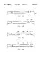
- FIG. 3A step by step development of the structure of a device with a pad film is shown in FIG. 3.
- the wafer 302has formed upon it landing electrodes 304a and 304b, and address electrodes 306a and 306b.
- the pad film 308is deposited, most likely by a planarized spin coat for flatness, over these electrodes.
- the landing electrodes 304 and address electrodes 306are at different biases and the pad film can prevent particulate matter from making contact between them, causing shorts.
- the spacer layer 310is deposited and etched to form the structure over which a metal layer will be deposited.
- the spaceris patterned and etched to form the post via 311, which will be filled in with metal.
- the first metal layeris deposited, it is patterned and etched to form the post 314.
- the mirror 312 and hinges 313are formed from a second metal layer deposited after patterning the first metal layer.
- air gap 316is left, allowing the mirror to move freely and deflect to land upon either landing electrode. Note that the post for the mirror shown in the final step would be positioned directly in front of the mirror between the viewer and the mirror.
- FIG. 4shows variations on the placement of the pad film depending upon the requirements of the process and the devices to be fabricated.
- the pad film 402since it is electrically insulative, could be formed over the entire activation circuitry. Depending upon the flexibility of the process, it could also be patterned and etched to form only pads at the points of contact between the mirror and the landing electrodes, 404aand 404b. Additionally, to allow for better insulation, it could be formed over the landing electrodes 404aand 404b, and over the addressing electrodes at 406a and 406b. For particulate insulation the film could be left over the addressing electrodes as in 408a and 408b, with just the pads on the landing electrodes 404aand 404b. Of course, combinations of any of the above could be used as needed by the device or the process.
- the digital micromirror devicecould represent the worst case for a micromechanical device. It has oppositely biased voltages within extremely close proximity to each other and high surface area contact points between the moving and non-moving parts of the device, which come into contact repeatedly.
- the use of the DMD as an exampleis in no way intended to limit the application of this pad film. Its usefulness applies across the range of micromechanical devices for insulation and particulate prevention, in addition to preventing frictional wear and sticking of moving parts.
Landscapes
- Physics & Mathematics (AREA)
- General Physics & Mathematics (AREA)
- Optics & Photonics (AREA)
- Mechanical Light Control Or Optical Switches (AREA)
Abstract
Description
This is a X division, of application Ser. No. 08/311,480, filed Sep. 23, 1994.
1. Field of the Invention
This invention relates to an improved method for manufacturing micromechanical devices, more particularly to manufacturing these devices such that their moving parts do not stick together.
2. Background of the Invention
Micromechanical devices are very small devices such as motors, gears, light modulator cells, etc., that are manufactured out of a semiconductor substrate, typically by a repeated process of masking and etching. They are activated by circuitry implanted into, or laid down upon, the substrate. As electronics move towards more and more power in a smaller and smaller space, micromechanical devices become more important.
One problem with these devices is the wear and tear they undergo during operation. A typical silicon micromotor loses its rotor after only about ten thousand revolutions. The silicon just wears away. The erosion is caused by the rotor sticking to surrounding structures, including its own axle, as it revolves, eating away the silicon. Another problem can occur when, instead of the rotor being worn away, it just sticks such that it will no longer move. Various methods of laying down protective layers exist, but each have their problems.
Some manufacturing processes use a deposited film on the devices after they are complete. Others try to work the layer into the existing process, requiring expensive and non-standard processing. Obviously, some method of preventing these devices from sticking together is needed.
An additional problem with micromechanical devices is the size of the activation circuitry. For example, micromechanical light modulators, such as the digital micromirror device, sometimes require activation circuitry of four electrodes for each 17 μ2 mirror. The mirror is suspended above its electrodes by hinges which in turn are supported by posts. Using the axis of the hinges as the center line of the mirror, each mirror has two electrodes on either side of its center line, directly under the mirror on the substrate. One electrode on each side is the addressing electrode, the other is the landing electrode, with the addressing electrodes adjacent to the center.
The landing electrodes and the mirror are held at the same bias voltage, preventing shorts or current flow when the mirrors touch their landing electrodes. In order to cause the mirror to deflect and touch the landing electrode, the address electrodes are set at a different bias. Because the area on the substrate within which these electrodes must reside is so close, it is relatively common for a particle to rest such that it touches both the landing electrodes and the address electrodes. Since they are held at different voltage levels, this can cause shorts in the activation circuitry of the modulator, rendering it unusable. Other micromechanical devices can suffer from these same problems, whenever the driving circuitry is close enough to allow particles or debris to cause shorts.
Therefore, a method is needed that allows micromechanical devices to run for longer period of time without sticking together, thereby causing wear. Additionally, it would be beneficial if the method preventing particulates and debris from damaging the circuitry which activates the micromechanical devices.
The described embodiments of the invention is a method for manufacturing micromechanical devices. The method includes the step of forming a pad film upon the activation circuitry and those structures that contact the moving parts of micromechanical devices. The film upon the activation circuitry acts as both a protective coating against particulates and an insulator between oppositely biased circuit paths. The film upon those structures of the device that contact the moving parts prevents wear and sticking of the moving parts. It is an advantage of the invention that it can be added to the existing manufacturing process with relative ease and no substantial increase in cost.
For a more complete understanding of the present invention and for further advantages thereof, reference is now made to the following Detailed Description taken in conjunction with the accompanying Drawings in which:
FIG. 1 is a prior art flow chart for the manufacture of a micromechanical device.
FIG. 2 is a flow chart of a process that includes a protective coating.
FIG. 3 a substrate as it goes through the various steps of a micromechanical device manufacturing process including a protective coating.
FIG. 4 shows different possibilities for the placement of a protective coating relative to the activation circuitry of a micromechanical device.
FIG. 1 shows an example of a prior art process for manufacturing a micromechanical device, specifically the digital micromirror device (DMD). Many other types of micromechanical devices can be manufactured using similar techniques. However, due to the unique nature and the high amount of contact between the parts, DMDs could represent the worst case for both particulates and for sticking parts.
Instep 101, the activation circuitry is formed on a wafer. Most of the processing will be performed at the wafer level. The activation circuitry could be implanted, deposited or otherwise formed on the circuitry. This circuitry might include address lines for an array of elements, voltage lines for motors, etc. For the DMD, the activation circuitry typically includes address lines in CMOS and a metal layer of electrodes.
The structure of the micromechanical device is begun instep 102. Vias are cut into the surface of the spacer for DMDs to make holes for posts, normally by an etching process. However, for other devices, such as micromotors, a silicon axle or rotor may be formed first, either by etching the silicon away from the rotor, or depositing more silicon. At some step in the process, however, some sort of spacer layer must be used to facilitate the manufacture of the moving parts.
For the DMD, the spacer will be patterned and etched to form vias. These vias will be filled with metal instep 103, which is the next layer of the device. The metal filled holes become support posts upon which the hinges will be formed to hold the mirrors. The next step withinstep 103 for the DMD is to pattern the metal layer holding the posts and removing the metal not used for the posts. A second layer of metal is deposited to form the hinges, and a final layer deposited to form the mirror itself (also known as the reflective surface or the beam).
At this point the mirror is complete with hinges and posts. Holes are patterned into the mirror to allow access to the spacer. The mirror still rests upon the spacer layer deposited instep 102. In DMD fabrication, this is typically removed using a plasma etch, leaving the mirror suspended over an air gap that allows the mirror to deflect freely from side to side.
Instep 105 the surfaces are passivated with a material that prevents sticking and frictional wear of the moving surfaces. However, it is becoming apparent that this passivation in and of itself is not enough. These devices are typically used in high resolution televisions and printers. When an individual mirror sticks to the electrodes, or does not have operable addressing circuitry because of a short, the picture suffers from pixel defects where the pixels in the picture are either white or black all of the time.
FIG. 2 shows one embodiment of the invention. This embodiment is a method of manufacture for micromechanical devices. After the activation circuitry is formed upon the wafer it is coated with a pad film, which is then patterned and etched as necessary. A pad film merely comprises a thin layer of material formed into a cushion. This protects the activation circuitry from particulate matter and prevents shorts. Additionally, if the activation circuitry or any underlying circuitry makes contact with any of the moving parts of the device, this will prevent frictional wear and sticking of the parts.
The process continues throughsteps step 204, any moving parts formed in the later steps of the process, such as a rotor or flywheel, or the non-moving parts that come in contact with the moving parts, could also be coated with a pad film. Again, this prevents sticking and frictional wear of the parts.
The composition of the pad film is only limited by the processes in which it is deposited and etched. However, desirable properties of this film are: low surface tension; temperature stability up to 110° C.; high abrasion resistance; high humidity resistance; and high surface stability. An example, which is in no way intended to limit the scope of the range of these materials, of such a material is a fluoropolymer. Additionally, the material could be other organic materials, such as other polymers, or inorganic material such as a nitride or oxide.
In tests of this type of material in such a process the following results were achieved:
______________________________________ Number of defective mirrors Device 1 hour 69 hours 391 hours 716 hours ______________________________________ Conventional 0 30 56 136 With pad film 0 11 12 30 ______________________________________
A step by step development of the structure of a device with a pad film is shown in FIG. 3. Thewafer 302 has formed upon it landingelectrodes electrodes pad film 308 is deposited, most likely by a planarized spin coat for flatness, over these electrodes. The landing electrodes 304 and address electrodes 306 are at different biases and the pad film can prevent particulate matter from making contact between them, causing shorts.
Thespacer layer 310 is deposited and etched to form the structure over which a metal layer will be deposited. The spacer is patterned and etched to form the post via 311, which will be filled in with metal. When the first metal layer is deposited, it is patterned and etched to form thepost 314. Themirror 312 and hinges 313 are formed from a second metal layer deposited after patterning the first metal layer. When the spacer is removed in the final step,air gap 316 is left, allowing the mirror to move freely and deflect to land upon either landing electrode. Note that the post for the mirror shown in the final step would be positioned directly in front of the mirror between the viewer and the mirror.
FIG. 4 shows variations on the placement of the pad film depending upon the requirements of the process and the devices to be fabricated. Thepad film 402, since it is electrically insulative, could be formed over the entire activation circuitry. Depending upon the flexibility of the process, it could also be patterned and etched to form only pads at the points of contact between the mirror and the landing electrodes,404aand 404b. Additionally, to allow for better insulation, it could be formed over the landing electrodes 404aand 404b, and over the addressing electrodes at 406a and 406b. For particulate insulation the film could be left over the addressing electrodes as in 408a and 408b, with just the pads on the landing electrodes 404aand 404b. Of course, combinations of any of the above could be used as needed by the device or the process.
As discussed previously, the digital micromirror device could represent the worst case for a micromechanical device. It has oppositely biased voltages within extremely close proximity to each other and high surface area contact points between the moving and non-moving parts of the device, which come into contact repeatedly. The use of the DMD as an example is in no way intended to limit the application of this pad film. Its usefulness applies across the range of micromechanical devices for insulation and particulate prevention, in addition to preventing frictional wear and sticking of moving parts.
Thus, although there has been described to this point particular embodiments of a process and device using a pad film, it is not intended that such specific references be considered as limitations upon the scope of this invention except in-so-far as set forth in the following claims.
Claims (4)
1. A method for manufacturing a digital micromirror device, wherein said method comprises:
forming activation circuitry upon a semiconductor wafer, wherein said activation circuitry includes surfaces with a first bias and surfaces with a second bias;
depositing an inorganic pad film upon said activation circuitry, wherein said pad film acts as an insulator between said surfaces having said first bias and said surfaces having said second bias;
building a spacer layer upon said pad film;
cutting vias into said spacer layer;
laying a first metal layer upon said spacer layer such that said first metal fills said vias;
depositing a second metal layer upon said first metal layer and patterning and etching said second layer to form mirrors and hinges; and
removing said spacer layer such that said mirror is held at said second bias and is suspended over said activation circuitry by said hinges and when activated contacts said surfaces having said second bias.
2. The method of claim 1 wherein said inorganic material is a nitride.
3. The method of claim 1 wherein said inorganic material is an oxide.
4. A micromechanical device comprising:
activation circuitry formed upon a semiconductor wafer;
posts formed adjacent said activation circuitry;
a mirror suspended from hinges on said posts, such that said mirror is operable to be activated by elements of said activation circuitry that have a first bias and will make contact with some elements of said activation circuitry held at a common second bias with said mirror when said mirror deflects; and
an inorganic pad film formed upon at least part of said activation circuitry such that said inorganic pad film acts as an insulator between said elements at said first bias, said elements at said second bias and said mirror.
Priority Applications (1)
| Application Number | Priority Date | Filing Date | Title |
|---|---|---|---|
| US08/483,777US6099132A (en) | 1994-09-23 | 1995-06-07 | Manufacture method for micromechanical devices |
Applications Claiming Priority (2)
| Application Number | Priority Date | Filing Date | Title |
|---|---|---|---|
| US08/311,480US6053617A (en) | 1994-09-23 | 1994-09-23 | Manufacture method for micromechanical devices |
| US08/483,777US6099132A (en) | 1994-09-23 | 1995-06-07 | Manufacture method for micromechanical devices |
Related Parent Applications (1)
| Application Number | Title | Priority Date | Filing Date |
|---|---|---|---|
| US08/311,480DivisionUS6053617A (en) | 1994-09-23 | 1994-09-23 | Manufacture method for micromechanical devices |
Publications (1)
| Publication Number | Publication Date |
|---|---|
| US6099132Atrue US6099132A (en) | 2000-08-08 |
Family
ID=23207063
Family Applications (2)
| Application Number | Title | Priority Date | Filing Date |
|---|---|---|---|
| US08/311,480Expired - LifetimeUS6053617A (en) | 1994-09-23 | 1994-09-23 | Manufacture method for micromechanical devices |
| US08/483,777Expired - LifetimeUS6099132A (en) | 1994-09-23 | 1995-06-07 | Manufacture method for micromechanical devices |
Family Applications Before (1)
| Application Number | Title | Priority Date | Filing Date |
|---|---|---|---|
| US08/311,480Expired - LifetimeUS6053617A (en) | 1994-09-23 | 1994-09-23 | Manufacture method for micromechanical devices |
Country Status (1)
| Country | Link |
|---|---|
| US (2) | US6053617A (en) |
Cited By (170)
| Publication number | Priority date | Publication date | Assignee | Title |
|---|---|---|---|---|
| US6257491B1 (en)* | 1993-10-25 | 2001-07-10 | Symbol Technologies, Inc. | Packaged mirror including mirror travel stops |
| WO2002016997A1 (en)* | 2000-08-18 | 2002-02-28 | Alcatel Optronics Uk Limited | Mem device |
| US6396619B1 (en) | 2000-01-28 | 2002-05-28 | Reflectivity, Inc. | Deflectable spatial light modulator having stopping mechanisms |
| US6741383B2 (en) | 2000-08-11 | 2004-05-25 | Reflectivity, Inc. | Deflectable micromirrors with stopping mechanisms |
| US7012732B2 (en) | 1994-05-05 | 2006-03-14 | Idc, Llc | Method and device for modulating light with a time-varying signal |
| US7012726B1 (en) | 2003-11-03 | 2006-03-14 | Idc, Llc | MEMS devices with unreleased thin film components |
| US7042643B2 (en) | 1994-05-05 | 2006-05-09 | Idc, Llc | Interferometric modulation of radiation |
| US7060895B2 (en) | 2004-05-04 | 2006-06-13 | Idc, Llc | Modifying the electro-mechanical behavior of devices |
| US7110158B2 (en) | 1999-10-05 | 2006-09-19 | Idc, Llc | Photonic MEMS and structures |
| US7119945B2 (en) | 2004-03-03 | 2006-10-10 | Idc, Llc | Altering temporal response of microelectromechanical elements |
| US7123216B1 (en) | 1994-05-05 | 2006-10-17 | Idc, Llc | Photonic MEMS and structures |
| US7130104B2 (en) | 2004-09-27 | 2006-10-31 | Idc, Llc | Methods and devices for inhibiting tilting of a mirror in an interferometric modulator |
| US7136213B2 (en) | 2004-09-27 | 2006-11-14 | Idc, Llc | Interferometric modulators having charge persistence |
| US7138984B1 (en) | 2001-06-05 | 2006-11-21 | Idc, Llc | Directly laminated touch sensitive screen |
| US7142346B2 (en) | 2003-12-09 | 2006-11-28 | Idc, Llc | System and method for addressing a MEMS display |
| US7161728B2 (en) | 2003-12-09 | 2007-01-09 | Idc, Llc | Area array modulation and lead reduction in interferometric modulators |
| US7161730B2 (en) | 2004-09-27 | 2007-01-09 | Idc, Llc | System and method for providing thermal compensation for an interferometric modulator display |
| US7164520B2 (en) | 2004-05-12 | 2007-01-16 | Idc, Llc | Packaging for an interferometric modulator |
| US7172915B2 (en) | 2003-01-29 | 2007-02-06 | Qualcomm Mems Technologies Co., Ltd. | Optical-interference type display panel and method for making the same |
| US7193768B2 (en) | 2003-08-26 | 2007-03-20 | Qualcomm Mems Technologies, Inc. | Interference display cell |
| US20070066063A1 (en)* | 2005-09-20 | 2007-03-22 | Texas Instruments Inc. | Method for chemical mechanical planarization of a metal layer located over a photoresist layer and a method for manufacturing a micro pixel array using the same |
| US7198973B2 (en) | 2003-04-21 | 2007-04-03 | Qualcomm Mems Technologies, Inc. | Method for fabricating an interference display unit |
| US7221495B2 (en) | 2003-06-24 | 2007-05-22 | Idc Llc | Thin film precursor stack for MEMS manufacturing |
| US7250315B2 (en) | 2002-02-12 | 2007-07-31 | Idc, Llc | Method for fabricating a structure for a microelectromechanical system (MEMS) device |
| US7256922B2 (en) | 2004-07-02 | 2007-08-14 | Idc, Llc | Interferometric modulators with thin film transistors |
| US7259865B2 (en) | 2004-09-27 | 2007-08-21 | Idc, Llc | Process control monitors for interferometric modulators |
| US7259449B2 (en) | 2004-09-27 | 2007-08-21 | Idc, Llc | Method and system for sealing a substrate |
| US7289256B2 (en) | 2004-09-27 | 2007-10-30 | Idc, Llc | Electrical characterization of interferometric modulators |
| US7289259B2 (en) | 2004-09-27 | 2007-10-30 | Idc, Llc | Conductive bus structure for interferometric modulator array |
| US7291921B2 (en) | 2003-09-30 | 2007-11-06 | Qualcomm Mems Technologies, Inc. | Structure of a micro electro mechanical system and the manufacturing method thereof |
| US7297471B1 (en) | 2003-04-15 | 2007-11-20 | Idc, Llc | Method for manufacturing an array of interferometric modulators |
| US7302157B2 (en) | 2004-09-27 | 2007-11-27 | Idc, Llc | System and method for multi-level brightness in interferometric modulation |
| US7299681B2 (en) | 2004-09-27 | 2007-11-27 | Idc, Llc | Method and system for detecting leak in electronic devices |
| US7304784B2 (en) | 2004-09-27 | 2007-12-04 | Idc, Llc | Reflective display device having viewable display on both sides |
| US7310179B2 (en) | 2004-09-27 | 2007-12-18 | Idc, Llc | Method and device for selective adjustment of hysteresis window |
| US7317568B2 (en) | 2004-09-27 | 2008-01-08 | Idc, Llc | System and method of implementation of interferometric modulators for display mirrors |
| US7321456B2 (en) | 2004-09-27 | 2008-01-22 | Idc, Llc | Method and device for corner interferometric modulation |
| US7321457B2 (en) | 2006-06-01 | 2008-01-22 | Qualcomm Incorporated | Process and structure for fabrication of MEMS device having isolated edge posts |
| US7327510B2 (en) | 2004-09-27 | 2008-02-05 | Idc, Llc | Process for modifying offset voltage characteristics of an interferometric modulator |
| US7343080B2 (en) | 2004-09-27 | 2008-03-11 | Idc, Llc | System and method of testing humidity in a sealed MEMS device |
| US7345805B2 (en) | 2004-09-27 | 2008-03-18 | Idc, Llc | Interferometric modulator array with integrated MEMS electrical switches |
| US7349139B2 (en) | 2004-09-27 | 2008-03-25 | Idc, Llc | System and method of illuminating interferometric modulators using backlighting |
| US7349136B2 (en) | 2004-09-27 | 2008-03-25 | Idc, Llc | Method and device for a display having transparent components integrated therein |
| US7355779B2 (en) | 2005-09-02 | 2008-04-08 | Idc, Llc | Method and system for driving MEMS display elements |
| US7359066B2 (en) | 2004-09-27 | 2008-04-15 | Idc, Llc | Electro-optical measurement of hysteresis in interferometric modulators |
| US7368803B2 (en) | 2004-09-27 | 2008-05-06 | Idc, Llc | System and method for protecting microelectromechanical systems array using back-plate with non-flat portion |
| US7369296B2 (en) | 2004-09-27 | 2008-05-06 | Idc, Llc | Device and method for modifying actuation voltage thresholds of a deformable membrane in an interferometric modulator |
| US7369294B2 (en) | 2004-09-27 | 2008-05-06 | Idc, Llc | Ornamental display device |
| US7369292B2 (en) | 2006-05-03 | 2008-05-06 | Qualcomm Mems Technologies, Inc. | Electrode and interconnect materials for MEMS devices |
| US7372613B2 (en) | 2004-09-27 | 2008-05-13 | Idc, Llc | Method and device for multistate interferometric light modulation |
| US7373026B2 (en) | 2004-09-27 | 2008-05-13 | Idc, Llc | MEMS device fabricated on a pre-patterned substrate |
| US7382515B2 (en) | 2006-01-18 | 2008-06-03 | Qualcomm Mems Technologies, Inc. | Silicon-rich silicon nitrides as etch stops in MEMS manufacture |
| US7385744B2 (en) | 2006-06-28 | 2008-06-10 | Qualcomm Mems Technologies, Inc. | Support structure for free-standing MEMS device and methods for forming the same |
| US7388704B2 (en) | 2006-06-30 | 2008-06-17 | Qualcomm Mems Technologies, Inc. | Determination of interferometric modulator mirror curvature and airgap variation using digital photographs |
| USRE40436E1 (en) | 2001-08-01 | 2008-07-15 | Idc, Llc | Hermetic seal and method to create the same |
| US7405924B2 (en) | 2004-09-27 | 2008-07-29 | Idc, Llc | System and method for protecting microelectromechanical systems array using structurally reinforced back-plate |
| US7405861B2 (en) | 2004-09-27 | 2008-07-29 | Idc, Llc | Method and device for protecting interferometric modulators from electrostatic discharge |
| US7405863B2 (en) | 2006-06-01 | 2008-07-29 | Qualcomm Mems Technologies, Inc. | Patterning of mechanical layer in MEMS to reduce stresses at supports |
| US7415186B2 (en) | 2004-09-27 | 2008-08-19 | Idc, Llc | Methods for visually inspecting interferometric modulators for defects |
| US7417735B2 (en) | 2004-09-27 | 2008-08-26 | Idc, Llc | Systems and methods for measuring color and contrast in specular reflective devices |
| US7417783B2 (en) | 2004-09-27 | 2008-08-26 | Idc, Llc | Mirror and mirror layer for optical modulator and method |
| US7417784B2 (en) | 2006-04-19 | 2008-08-26 | Qualcomm Mems Technologies, Inc. | Microelectromechanical device and method utilizing a porous surface |
| US7420725B2 (en) | 2004-09-27 | 2008-09-02 | Idc, Llc | Device having a conductive light absorbing mask and method for fabricating same |
| US7420728B2 (en) | 2004-09-27 | 2008-09-02 | Idc, Llc | Methods of fabricating interferometric modulators by selectively removing a material |
| US7424198B2 (en) | 2004-09-27 | 2008-09-09 | Idc, Llc | Method and device for packaging a substrate |
| US7446927B2 (en) | 2004-09-27 | 2008-11-04 | Idc, Llc | MEMS switch with set and latch electrodes |
| US7450295B2 (en) | 2006-03-02 | 2008-11-11 | Qualcomm Mems Technologies, Inc. | Methods for producing MEMS with protective coatings using multi-component sacrificial layers |
| US7453579B2 (en) | 2004-09-27 | 2008-11-18 | Idc, Llc | Measurement of the dynamic characteristics of interferometric modulators |
| US7460246B2 (en) | 2004-09-27 | 2008-12-02 | Idc, Llc | Method and system for sensing light using interferometric elements |
| US7460291B2 (en) | 1994-05-05 | 2008-12-02 | Idc, Llc | Separable modulator |
| US20080311690A1 (en)* | 2007-04-04 | 2008-12-18 | Qualcomm Mems Technologies, Inc. | Eliminate release etch attack by interface modification in sacrificial layers |
| US7471442B2 (en) | 2006-06-15 | 2008-12-30 | Qualcomm Mems Technologies, Inc. | Method and apparatus for low range bit depth enhancements for MEMS display architectures |
| US7471444B2 (en) | 1996-12-19 | 2008-12-30 | Idc, Llc | Interferometric modulation of radiation |
| US20090002804A1 (en)* | 2007-06-29 | 2009-01-01 | Qualcomm Mems Technologies, Inc. | Electromechanical device treatment with water vapor |
| US7476327B2 (en) | 2004-05-04 | 2009-01-13 | Idc, Llc | Method of manufacture for microelectromechanical devices |
| US7486429B2 (en) | 2004-09-27 | 2009-02-03 | Idc, Llc | Method and device for multistate interferometric light modulation |
| US7492502B2 (en) | 2004-09-27 | 2009-02-17 | Idc, Llc | Method of fabricating a free-standing microstructure |
| US7499208B2 (en) | 2004-08-27 | 2009-03-03 | Udc, Llc | Current mode display driver circuit realization feature |
| US7515147B2 (en) | 2004-08-27 | 2009-04-07 | Idc, Llc | Staggered column drive circuit systems and methods |
| US7527998B2 (en) | 2006-06-30 | 2009-05-05 | Qualcomm Mems Technologies, Inc. | Method of manufacturing MEMS devices providing air gap control |
| US7527995B2 (en) | 2004-09-27 | 2009-05-05 | Qualcomm Mems Technologies, Inc. | Method of making prestructure for MEMS systems |
| US7527996B2 (en) | 2006-04-19 | 2009-05-05 | Qualcomm Mems Technologies, Inc. | Non-planar surface structures and process for microelectromechanical systems |
| US7532195B2 (en) | 2004-09-27 | 2009-05-12 | Idc, Llc | Method and system for reducing power consumption in a display |
| US7532194B2 (en) | 2004-02-03 | 2009-05-12 | Idc, Llc | Driver voltage adjuster |
| US7532377B2 (en) | 1998-04-08 | 2009-05-12 | Idc, Llc | Movable micro-electromechanical device |
| US7534640B2 (en) | 2005-07-22 | 2009-05-19 | Qualcomm Mems Technologies, Inc. | Support structure for MEMS device and methods therefor |
| US7535621B2 (en) | 2006-12-27 | 2009-05-19 | Qualcomm Mems Technologies, Inc. | Aluminum fluoride films for microelectromechanical system applications |
| US7535466B2 (en) | 2004-09-27 | 2009-05-19 | Idc, Llc | System with server based control of client device display features |
| US7545550B2 (en) | 2004-09-27 | 2009-06-09 | Idc, Llc | Systems and methods of actuating MEMS display elements |
| US7547565B2 (en) | 2005-02-04 | 2009-06-16 | Qualcomm Mems Technologies, Inc. | Method of manufacturing optical interference color display |
| US7547568B2 (en) | 2006-02-22 | 2009-06-16 | Qualcomm Mems Technologies, Inc. | Electrical conditioning of MEMS device and insulating layer thereof |
| US7551159B2 (en) | 2004-08-27 | 2009-06-23 | Idc, Llc | System and method of sensing actuation and release voltages of an interferometric modulator |
| US7550810B2 (en) | 2006-02-23 | 2009-06-23 | Qualcomm Mems Technologies, Inc. | MEMS device having a layer movable at asymmetric rates |
| US7550794B2 (en) | 2002-09-20 | 2009-06-23 | Idc, Llc | Micromechanical systems device comprising a displaceable electrode and a charge-trapping layer |
| US7553684B2 (en) | 2004-09-27 | 2009-06-30 | Idc, Llc | Method of fabricating interferometric devices using lift-off processing techniques |
| US7554711B2 (en) | 1998-04-08 | 2009-06-30 | Idc, Llc. | MEMS devices with stiction bumps |
| US7554714B2 (en) | 2004-09-27 | 2009-06-30 | Idc, Llc | Device and method for manipulation of thermal response in a modulator |
| US7560299B2 (en) | 2004-08-27 | 2009-07-14 | Idc, Llc | Systems and methods of actuating MEMS display elements |
| US7564612B2 (en) | 2004-09-27 | 2009-07-21 | Idc, Llc | Photonic MEMS and structures |
| US7567373B2 (en) | 2004-07-29 | 2009-07-28 | Idc, Llc | System and method for micro-electromechanical operation of an interferometric modulator |
| US7566664B2 (en) | 2006-08-02 | 2009-07-28 | Qualcomm Mems Technologies, Inc. | Selective etching of MEMS using gaseous halides and reactive co-etchants |
| US7570415B2 (en) | 2007-08-07 | 2009-08-04 | Qualcomm Mems Technologies, Inc. | MEMS device and interconnects for same |
| US7580172B2 (en) | 2005-09-30 | 2009-08-25 | Qualcomm Mems Technologies, Inc. | MEMS device and interconnects for same |
| US7582952B2 (en) | 2006-02-21 | 2009-09-01 | Qualcomm Mems Technologies, Inc. | Method for providing and removing discharging interconnect for chip-on-glass output leads and structures thereof |
| US7586484B2 (en) | 2004-09-27 | 2009-09-08 | Idc, Llc | Controller and driver features for bi-stable display |
| US20090231668A1 (en)* | 2007-05-03 | 2009-09-17 | Yoshihiro Maeda | Mirror device with an anti-stiction layer |
| US7602375B2 (en) | 2004-09-27 | 2009-10-13 | Idc, Llc | Method and system for writing data to MEMS display elements |
| US7623287B2 (en) | 2006-04-19 | 2009-11-24 | Qualcomm Mems Technologies, Inc. | Non-planar surface structures and process for microelectromechanical systems |
| US7626581B2 (en) | 2004-09-27 | 2009-12-01 | Idc, Llc | Device and method for display memory using manipulation of mechanical response |
| US7630119B2 (en) | 2004-09-27 | 2009-12-08 | Qualcomm Mems Technologies, Inc. | Apparatus and method for reducing slippage between structures in an interferometric modulator |
| US7630114B2 (en) | 2005-10-28 | 2009-12-08 | Idc, Llc | Diffusion barrier layer for MEMS devices |
| US20090305010A1 (en)* | 2008-06-05 | 2009-12-10 | Qualcomm Mems Technologies, Inc. | Low temperature amorphous silicon sacrificial layer for controlled adhesion in mems devices |
| US7636151B2 (en) | 2006-01-06 | 2009-12-22 | Qualcomm Mems Technologies, Inc. | System and method for providing residual stress test structures |
| US7643203B2 (en) | 2006-04-10 | 2010-01-05 | Qualcomm Mems Technologies, Inc. | Interferometric optical display system with broadband characteristics |
| US7649671B2 (en) | 2006-06-01 | 2010-01-19 | Qualcomm Mems Technologies, Inc. | Analog interferometric modulator device with electrostatic actuation and release |
| US7653371B2 (en) | 2004-09-27 | 2010-01-26 | Qualcomm Mems Technologies, Inc. | Selectable capacitance circuit |
| US7652814B2 (en) | 2006-01-27 | 2010-01-26 | Qualcomm Mems Technologies, Inc. | MEMS device with integrated optical element |
| US7660058B2 (en) | 2005-08-19 | 2010-02-09 | Qualcomm Mems Technologies, Inc. | Methods for etching layers within a MEMS device to achieve a tapered edge |
| US7668415B2 (en) | 2004-09-27 | 2010-02-23 | Qualcomm Mems Technologies, Inc. | Method and device for providing electronic circuitry on a backplate |
| US7675669B2 (en) | 2004-09-27 | 2010-03-09 | Qualcomm Mems Technologies, Inc. | Method and system for driving interferometric modulators |
| US7679627B2 (en) | 2004-09-27 | 2010-03-16 | Qualcomm Mems Technologies, Inc. | Controller and driver features for bi-stable display |
| US7684104B2 (en) | 2004-09-27 | 2010-03-23 | Idc, Llc | MEMS using filler material and method |
| US7692839B2 (en) | 2004-09-27 | 2010-04-06 | Qualcomm Mems Technologies, Inc. | System and method of providing MEMS device with anti-stiction coating |
| US7702192B2 (en) | 2006-06-21 | 2010-04-20 | Qualcomm Mems Technologies, Inc. | Systems and methods for driving MEMS display |
| US7701631B2 (en) | 2004-09-27 | 2010-04-20 | Qualcomm Mems Technologies, Inc. | Device having patterned spacers for backplates and method of making the same |
| US7706050B2 (en) | 2004-03-05 | 2010-04-27 | Qualcomm Mems Technologies, Inc. | Integrated modulator illumination |
| US7706044B2 (en) | 2003-05-26 | 2010-04-27 | Qualcomm Mems Technologies, Inc. | Optical interference display cell and method of making the same |
| US7710629B2 (en) | 2004-09-27 | 2010-05-04 | Qualcomm Mems Technologies, Inc. | System and method for display device with reinforcing substance |
| US7711239B2 (en) | 2006-04-19 | 2010-05-04 | Qualcomm Mems Technologies, Inc. | Microelectromechanical device and method utilizing nanoparticles |
| US7719500B2 (en) | 2004-09-27 | 2010-05-18 | Qualcomm Mems Technologies, Inc. | Reflective display pixels arranged in non-rectangular arrays |
| US7719752B2 (en) | 2007-05-11 | 2010-05-18 | Qualcomm Mems Technologies, Inc. | MEMS structures, methods of fabricating MEMS components on separate substrates and assembly of same |
| US7724993B2 (en) | 2004-09-27 | 2010-05-25 | Qualcomm Mems Technologies, Inc. | MEMS switches with deforming membranes |
| US7733552B2 (en) | 2007-03-21 | 2010-06-08 | Qualcomm Mems Technologies, Inc | MEMS cavity-coating layers and methods |
| US7763546B2 (en) | 2006-08-02 | 2010-07-27 | Qualcomm Mems Technologies, Inc. | Methods for reducing surface charges during the manufacture of microelectromechanical systems devices |
| US7777715B2 (en) | 2006-06-29 | 2010-08-17 | Qualcomm Mems Technologies, Inc. | Passive circuits for de-multiplexing display inputs |
| US7781850B2 (en) | 2002-09-20 | 2010-08-24 | Qualcomm Mems Technologies, Inc. | Controlling electromechanical behavior of structures within a microelectromechanical systems device |
| US7795061B2 (en) | 2005-12-29 | 2010-09-14 | Qualcomm Mems Technologies, Inc. | Method of creating MEMS device cavities by a non-etching process |
| US7808703B2 (en) | 2004-09-27 | 2010-10-05 | Qualcomm Mems Technologies, Inc. | System and method for implementation of interferometric modulator displays |
| US7813026B2 (en) | 2004-09-27 | 2010-10-12 | Qualcomm Mems Technologies, Inc. | System and method of reducing color shift in a display |
| US7835061B2 (en) | 2006-06-28 | 2010-11-16 | Qualcomm Mems Technologies, Inc. | Support structures for free-standing electromechanical devices |
| US7843410B2 (en) | 2004-09-27 | 2010-11-30 | Qualcomm Mems Technologies, Inc. | Method and device for electrically programmable display |
| US7872394B1 (en) | 2001-12-13 | 2011-01-18 | Joseph E Ford | MEMS device with two axes comb drive actuators |
| USRE42119E1 (en) | 2002-02-27 | 2011-02-08 | Qualcomm Mems Technologies, Inc. | Microelectrochemical systems device and method for fabricating same |
| US7889163B2 (en) | 2004-08-27 | 2011-02-15 | Qualcomm Mems Technologies, Inc. | Drive method for MEMS devices |
| US7893919B2 (en) | 2004-09-27 | 2011-02-22 | Qualcomm Mems Technologies, Inc. | Display region architectures |
| US7903047B2 (en) | 2006-04-17 | 2011-03-08 | Qualcomm Mems Technologies, Inc. | Mode indicator for interferometric modulator displays |
| US7916980B2 (en) | 2006-01-13 | 2011-03-29 | Qualcomm Mems Technologies, Inc. | Interconnect structure for MEMS device |
| US7916103B2 (en) | 2004-09-27 | 2011-03-29 | Qualcomm Mems Technologies, Inc. | System and method for display device with end-of-life phenomena |
| US7920135B2 (en) | 2004-09-27 | 2011-04-05 | Qualcomm Mems Technologies, Inc. | Method and system for driving a bi-stable display |
| US7920136B2 (en) | 2005-05-05 | 2011-04-05 | Qualcomm Mems Technologies, Inc. | System and method of driving a MEMS display device |
| US7936497B2 (en) | 2004-09-27 | 2011-05-03 | Qualcomm Mems Technologies, Inc. | MEMS device having deformable membrane characterized by mechanical persistence |
| US7948457B2 (en) | 2005-05-05 | 2011-05-24 | Qualcomm Mems Technologies, Inc. | Systems and methods of actuating MEMS display elements |
| US8008736B2 (en) | 2004-09-27 | 2011-08-30 | Qualcomm Mems Technologies, Inc. | Analog interferometric modulator device |
| US8014059B2 (en) | 1994-05-05 | 2011-09-06 | Qualcomm Mems Technologies, Inc. | System and method for charge control in a MEMS device |
| US8049713B2 (en) | 2006-04-24 | 2011-11-01 | Qualcomm Mems Technologies, Inc. | Power consumption optimized display update |
| US8124434B2 (en) | 2004-09-27 | 2012-02-28 | Qualcomm Mems Technologies, Inc. | Method and system for packaging a display |
| US8174469B2 (en) | 2005-05-05 | 2012-05-08 | Qualcomm Mems Technologies, Inc. | Dynamic driver IC and display panel configuration |
| US8194056B2 (en) | 2006-02-09 | 2012-06-05 | Qualcomm Mems Technologies Inc. | Method and system for writing data to MEMS display elements |
| US8310441B2 (en) | 2004-09-27 | 2012-11-13 | Qualcomm Mems Technologies, Inc. | Method and system for writing data to MEMS display elements |
| US8391630B2 (en) | 2005-12-22 | 2013-03-05 | Qualcomm Mems Technologies, Inc. | System and method for power reduction when decompressing video streams for interferometric modulator displays |
| US20130327649A1 (en)* | 2011-02-22 | 2013-12-12 | Commissariat A L'energie Atomique Et Aux Energies Alternatives | Biosensor and Method of Manufacturing Such a Biosensor |
| US8735225B2 (en) | 2004-09-27 | 2014-05-27 | Qualcomm Mems Technologies, Inc. | Method and system for packaging MEMS devices with glass seal |
| US8736590B2 (en) | 2009-03-27 | 2014-05-27 | Qualcomm Mems Technologies, Inc. | Low voltage driver scheme for interferometric modulators |
| US8817357B2 (en) | 2010-04-09 | 2014-08-26 | Qualcomm Mems Technologies, Inc. | Mechanical layer and methods of forming the same |
| US8878825B2 (en) | 2004-09-27 | 2014-11-04 | Qualcomm Mems Technologies, Inc. | System and method for providing a variable refresh rate of an interferometric modulator display |
| US8885244B2 (en) | 2004-09-27 | 2014-11-11 | Qualcomm Mems Technologies, Inc. | Display device |
| US8928967B2 (en) | 1998-04-08 | 2015-01-06 | Qualcomm Mems Technologies, Inc. | Method and device for modulating light |
| US8963159B2 (en) | 2011-04-04 | 2015-02-24 | Qualcomm Mems Technologies, Inc. | Pixel via and methods of forming the same |
| US9001412B2 (en) | 2004-09-27 | 2015-04-07 | Qualcomm Mems Technologies, Inc. | Electromechanical device with optical function separated from mechanical and electrical function |
| US9134527B2 (en) | 2011-04-04 | 2015-09-15 | Qualcomm Mems Technologies, Inc. | Pixel via and methods of forming the same |
Families Citing this family (12)
| Publication number | Priority date | Publication date | Assignee | Title |
|---|---|---|---|---|
| US6046840A (en)* | 1995-06-19 | 2000-04-04 | Reflectivity, Inc. | Double substrate reflective spatial light modulator with self-limiting micro-mechanical elements |
| KR100708086B1 (en)* | 2000-06-03 | 2007-04-16 | 삼성전자주식회사 | Micromirror devices |
| KR20010109867A (en)* | 2000-06-03 | 2001-12-12 | 윤종용 | Micro-mirror device and method for manufacturing thereof |
| US7099065B2 (en)* | 2000-08-03 | 2006-08-29 | Reflectivity, Inc. | Micromirrors with OFF-angle electrodes and stops |
| US7405860B2 (en)* | 2002-11-26 | 2008-07-29 | Texas Instruments Incorporated | Spatial light modulators with light blocking/absorbing areas |
| US7787170B2 (en) | 2004-06-15 | 2010-08-31 | Texas Instruments Incorporated | Micromirror array assembly with in-array pillars |
| US7113322B2 (en)* | 2004-06-23 | 2006-09-26 | Reflectivity, Inc | Micromirror having offset addressing electrode |
| US7092143B2 (en)* | 2004-10-19 | 2006-08-15 | Reflectivity, Inc | Micromirror array device and a method for making the same |
| US7158279B2 (en)* | 2004-10-19 | 2007-01-02 | Texas Instruments Incorporated | Spatial light modulators with non-uniform pixels |
| US7295363B2 (en) | 2005-04-08 | 2007-11-13 | Texas Instruments Incorporated | Optical coating on light transmissive substrates of micromirror devices |
| US8791012B2 (en)* | 2007-03-21 | 2014-07-29 | Texas Instruments Incorporated | Methods and apparatus for manufacturing semiconductor devices |
| US20090243011A1 (en)* | 2008-03-26 | 2009-10-01 | Texas Instruments Incorporated | Manufacturing Optical MEMS with Thin-Film Anti-Reflective Layers |
Citations (8)
| Publication number | Priority date | Publication date | Assignee | Title |
|---|---|---|---|---|
| US4293377A (en)* | 1978-06-29 | 1981-10-06 | Rogers Corporation | Manufacturing method for circuit board |
| US4970106A (en)* | 1989-06-02 | 1990-11-13 | International Business Machines Corporation | Thin film multilayer laminate interconnection board |
| US5083857A (en)* | 1990-06-29 | 1992-01-28 | Texas Instruments Incorporated | Multi-level deformable mirror device |
| US5099353A (en)* | 1990-06-29 | 1992-03-24 | Texas Instruments Incorporated | Architecture and process for integrating DMD with control circuit substrates |
| US5142405A (en)* | 1990-06-29 | 1992-08-25 | Texas Instruments Incorporated | Bistable dmd addressing circuit and method |
| US5227013A (en)* | 1991-07-25 | 1993-07-13 | Microelectronics And Computer Technology Corporation | Forming via holes in a multilevel substrate in a single step |
| US5298114A (en)* | 1991-02-07 | 1994-03-29 | Fujitsu Limited | Thin film circuit substrate and process for the manufacture thereof |
| US5447600A (en)* | 1994-03-21 | 1995-09-05 | Texas Instruments | Polymeric coatings for micromechanical devices |
- 1994
- 1994-09-23USUS08/311,480patent/US6053617A/ennot_activeExpired - Lifetime
- 1995
- 1995-06-07USUS08/483,777patent/US6099132A/ennot_activeExpired - Lifetime
Patent Citations (8)
| Publication number | Priority date | Publication date | Assignee | Title |
|---|---|---|---|---|
| US4293377A (en)* | 1978-06-29 | 1981-10-06 | Rogers Corporation | Manufacturing method for circuit board |
| US4970106A (en)* | 1989-06-02 | 1990-11-13 | International Business Machines Corporation | Thin film multilayer laminate interconnection board |
| US5083857A (en)* | 1990-06-29 | 1992-01-28 | Texas Instruments Incorporated | Multi-level deformable mirror device |
| US5099353A (en)* | 1990-06-29 | 1992-03-24 | Texas Instruments Incorporated | Architecture and process for integrating DMD with control circuit substrates |
| US5142405A (en)* | 1990-06-29 | 1992-08-25 | Texas Instruments Incorporated | Bistable dmd addressing circuit and method |
| US5298114A (en)* | 1991-02-07 | 1994-03-29 | Fujitsu Limited | Thin film circuit substrate and process for the manufacture thereof |
| US5227013A (en)* | 1991-07-25 | 1993-07-13 | Microelectronics And Computer Technology Corporation | Forming via holes in a multilevel substrate in a single step |
| US5447600A (en)* | 1994-03-21 | 1995-09-05 | Texas Instruments | Polymeric coatings for micromechanical devices |
Cited By (233)
| Publication number | Priority date | Publication date | Assignee | Title |
|---|---|---|---|---|
| US6257491B1 (en)* | 1993-10-25 | 2001-07-10 | Symbol Technologies, Inc. | Packaged mirror including mirror travel stops |
| US7280265B2 (en) | 1994-05-05 | 2007-10-09 | Idc, Llc | Interferometric modulation of radiation |
| US7460291B2 (en) | 1994-05-05 | 2008-12-02 | Idc, Llc | Separable modulator |
| US7692844B2 (en) | 1994-05-05 | 2010-04-06 | Qualcomm Mems Technologies, Inc. | Interferometric modulation of radiation |
| US8014059B2 (en) | 1994-05-05 | 2011-09-06 | Qualcomm Mems Technologies, Inc. | System and method for charge control in a MEMS device |
| US7012732B2 (en) | 1994-05-05 | 2006-03-14 | Idc, Llc | Method and device for modulating light with a time-varying signal |
| US7042643B2 (en) | 1994-05-05 | 2006-05-09 | Idc, Llc | Interferometric modulation of radiation |
| US7372619B2 (en) | 1994-05-05 | 2008-05-13 | Idc, Llc | Display device having a movable structure for modulating light and method thereof |
| US8059326B2 (en) | 1994-05-05 | 2011-11-15 | Qualcomm Mems Technologies Inc. | Display devices comprising of interferometric modulator and sensor |
| US7379227B2 (en) | 1994-05-05 | 2008-05-27 | Idc, Llc | Method and device for modulating light |
| US7123216B1 (en) | 1994-05-05 | 2006-10-17 | Idc, Llc | Photonic MEMS and structures |
| US7236284B2 (en) | 1995-05-01 | 2007-06-26 | Idc, Llc | Photonic MEMS and structures |
| US7388706B2 (en) | 1995-05-01 | 2008-06-17 | Idc, Llc | Photonic MEMS and structures |
| US7471444B2 (en) | 1996-12-19 | 2008-12-30 | Idc, Llc | Interferometric modulation of radiation |
| US9110289B2 (en) | 1998-04-08 | 2015-08-18 | Qualcomm Mems Technologies, Inc. | Device for modulating light with multiple electrodes |
| US7554711B2 (en) | 1998-04-08 | 2009-06-30 | Idc, Llc. | MEMS devices with stiction bumps |
| US8928967B2 (en) | 1998-04-08 | 2015-01-06 | Qualcomm Mems Technologies, Inc. | Method and device for modulating light |
| US7532377B2 (en) | 1998-04-08 | 2009-05-12 | Idc, Llc | Movable micro-electromechanical device |
| US7483197B2 (en) | 1999-10-05 | 2009-01-27 | Idc, Llc | Photonic MEMS and structures |
| US7110158B2 (en) | 1999-10-05 | 2006-09-19 | Idc, Llc | Photonic MEMS and structures |
| US7355782B2 (en) | 1999-10-05 | 2008-04-08 | Idc, Llc | Systems and methods of controlling micro-electromechanical devices |
| US7830586B2 (en) | 1999-10-05 | 2010-11-09 | Qualcomm Mems Technologies, Inc. | Transparent thin films |
| US7187489B2 (en) | 1999-10-05 | 2007-03-06 | Idc, Llc | Photonic MEMS and structures |
| US6396619B1 (en) | 2000-01-28 | 2002-05-28 | Reflectivity, Inc. | Deflectable spatial light modulator having stopping mechanisms |
| US6741383B2 (en) | 2000-08-11 | 2004-05-25 | Reflectivity, Inc. | Deflectable micromirrors with stopping mechanisms |
| WO2002016997A1 (en)* | 2000-08-18 | 2002-02-28 | Alcatel Optronics Uk Limited | Mem device |
| US20040022482A1 (en)* | 2000-08-18 | 2004-02-05 | Paul Blair | Mem device |
| US7138984B1 (en) | 2001-06-05 | 2006-11-21 | Idc, Llc | Directly laminated touch sensitive screen |
| USRE40436E1 (en) | 2001-08-01 | 2008-07-15 | Idc, Llc | Hermetic seal and method to create the same |
| US7872394B1 (en) | 2001-12-13 | 2011-01-18 | Joseph E Ford | MEMS device with two axes comb drive actuators |
| US7250315B2 (en) | 2002-02-12 | 2007-07-31 | Idc, Llc | Method for fabricating a structure for a microelectromechanical system (MEMS) device |
| US7642110B2 (en) | 2002-02-12 | 2010-01-05 | Qualcomm Mems Technologies, Inc. | Method for fabricating a structure for a microelectromechanical systems (MEMS) device |
| USRE42119E1 (en) | 2002-02-27 | 2011-02-08 | Qualcomm Mems Technologies, Inc. | Microelectrochemical systems device and method for fabricating same |
| US7550794B2 (en) | 2002-09-20 | 2009-06-23 | Idc, Llc | Micromechanical systems device comprising a displaceable electrode and a charge-trapping layer |
| US7781850B2 (en) | 2002-09-20 | 2010-08-24 | Qualcomm Mems Technologies, Inc. | Controlling electromechanical behavior of structures within a microelectromechanical systems device |
| US7172915B2 (en) | 2003-01-29 | 2007-02-06 | Qualcomm Mems Technologies Co., Ltd. | Optical-interference type display panel and method for making the same |
| US7297471B1 (en) | 2003-04-15 | 2007-11-20 | Idc, Llc | Method for manufacturing an array of interferometric modulators |
| US7198973B2 (en) | 2003-04-21 | 2007-04-03 | Qualcomm Mems Technologies, Inc. | Method for fabricating an interference display unit |
| US7706044B2 (en) | 2003-05-26 | 2010-04-27 | Qualcomm Mems Technologies, Inc. | Optical interference display cell and method of making the same |
| US7616369B2 (en) | 2003-06-24 | 2009-11-10 | Idc, Llc | Film stack for manufacturing micro-electromechanical systems (MEMS) devices |
| US7221495B2 (en) | 2003-06-24 | 2007-05-22 | Idc Llc | Thin film precursor stack for MEMS manufacturing |
| US7193768B2 (en) | 2003-08-26 | 2007-03-20 | Qualcomm Mems Technologies, Inc. | Interference display cell |
| US7291921B2 (en) | 2003-09-30 | 2007-11-06 | Qualcomm Mems Technologies, Inc. | Structure of a micro electro mechanical system and the manufacturing method thereof |
| US7012726B1 (en) | 2003-11-03 | 2006-03-14 | Idc, Llc | MEMS devices with unreleased thin film components |
| US7161728B2 (en) | 2003-12-09 | 2007-01-09 | Idc, Llc | Area array modulation and lead reduction in interferometric modulators |
| US7242512B2 (en) | 2003-12-09 | 2007-07-10 | Idc, Llc | System and method for addressing a MEMS display |
| US7196837B2 (en) | 2003-12-09 | 2007-03-27 | Idc, Llc | Area array modulation and lead reduction in interferometric modulators |
| US7142346B2 (en) | 2003-12-09 | 2006-11-28 | Idc, Llc | System and method for addressing a MEMS display |
| US7388697B2 (en) | 2003-12-09 | 2008-06-17 | Idc, Llc | System and method for addressing a MEMS display |
| US7532194B2 (en) | 2004-02-03 | 2009-05-12 | Idc, Llc | Driver voltage adjuster |
| US7119945B2 (en) | 2004-03-03 | 2006-10-10 | Idc, Llc | Altering temporal response of microelectromechanical elements |
| US7706050B2 (en) | 2004-03-05 | 2010-04-27 | Qualcomm Mems Technologies, Inc. | Integrated modulator illumination |
| US7880954B2 (en) | 2004-03-05 | 2011-02-01 | Qualcomm Mems Technologies, Inc. | Integrated modulator illumination |
| US7060895B2 (en) | 2004-05-04 | 2006-06-13 | Idc, Llc | Modifying the electro-mechanical behavior of devices |
| US7161094B2 (en) | 2004-05-04 | 2007-01-09 | Idc, Llc | Modifying the electro-mechanical behavior of devices |
| US7476327B2 (en) | 2004-05-04 | 2009-01-13 | Idc, Llc | Method of manufacture for microelectromechanical devices |
| US8853747B2 (en) | 2004-05-12 | 2014-10-07 | Qualcomm Mems Technologies, Inc. | Method of making an electronic device with a curved backplate |
| US7164520B2 (en) | 2004-05-12 | 2007-01-16 | Idc, Llc | Packaging for an interferometric modulator |
| US7256922B2 (en) | 2004-07-02 | 2007-08-14 | Idc, Llc | Interferometric modulators with thin film transistors |
| US7567373B2 (en) | 2004-07-29 | 2009-07-28 | Idc, Llc | System and method for micro-electromechanical operation of an interferometric modulator |
| US7928940B2 (en) | 2004-08-27 | 2011-04-19 | Qualcomm Mems Technologies, Inc. | Drive method for MEMS devices |
| US7499208B2 (en) | 2004-08-27 | 2009-03-03 | Udc, Llc | Current mode display driver circuit realization feature |
| US7515147B2 (en) | 2004-08-27 | 2009-04-07 | Idc, Llc | Staggered column drive circuit systems and methods |
| US7551159B2 (en) | 2004-08-27 | 2009-06-23 | Idc, Llc | System and method of sensing actuation and release voltages of an interferometric modulator |
| US7889163B2 (en) | 2004-08-27 | 2011-02-15 | Qualcomm Mems Technologies, Inc. | Drive method for MEMS devices |
| US7560299B2 (en) | 2004-08-27 | 2009-07-14 | Idc, Llc | Systems and methods of actuating MEMS display elements |
| US7369252B2 (en) | 2004-09-27 | 2008-05-06 | Idc, Llc | Process control monitors for interferometric modulators |
| US7679627B2 (en) | 2004-09-27 | 2010-03-16 | Qualcomm Mems Technologies, Inc. | Controller and driver features for bi-stable display |
| US7130104B2 (en) | 2004-09-27 | 2006-10-31 | Idc, Llc | Methods and devices for inhibiting tilting of a mirror in an interferometric modulator |
| US9097885B2 (en) | 2004-09-27 | 2015-08-04 | Qualcomm Mems Technologies, Inc. | Device having a conductive light absorbing mask and method for fabricating same |
| US7403323B2 (en) | 2004-09-27 | 2008-07-22 | Idc, Llc | Process control monitors for interferometric modulators |
| US7405924B2 (en) | 2004-09-27 | 2008-07-29 | Idc, Llc | System and method for protecting microelectromechanical systems array using structurally reinforced back-plate |
| US7405861B2 (en) | 2004-09-27 | 2008-07-29 | Idc, Llc | Method and device for protecting interferometric modulators from electrostatic discharge |
| US9086564B2 (en) | 2004-09-27 | 2015-07-21 | Qualcomm Mems Technologies, Inc. | Conductive bus structure for interferometric modulator array |
| US7415186B2 (en) | 2004-09-27 | 2008-08-19 | Idc, Llc | Methods for visually inspecting interferometric modulators for defects |
| US7417735B2 (en) | 2004-09-27 | 2008-08-26 | Idc, Llc | Systems and methods for measuring color and contrast in specular reflective devices |
| US7417783B2 (en) | 2004-09-27 | 2008-08-26 | Idc, Llc | Mirror and mirror layer for optical modulator and method |
| US9001412B2 (en) | 2004-09-27 | 2015-04-07 | Qualcomm Mems Technologies, Inc. | Electromechanical device with optical function separated from mechanical and electrical function |
| US7420725B2 (en) | 2004-09-27 | 2008-09-02 | Idc, Llc | Device having a conductive light absorbing mask and method for fabricating same |
| US7420728B2 (en) | 2004-09-27 | 2008-09-02 | Idc, Llc | Methods of fabricating interferometric modulators by selectively removing a material |
| US7424198B2 (en) | 2004-09-27 | 2008-09-09 | Idc, Llc | Method and device for packaging a substrate |
| US8970939B2 (en) | 2004-09-27 | 2015-03-03 | Qualcomm Mems Technologies, Inc. | Method and device for multistate interferometric light modulation |
| US7429334B2 (en) | 2004-09-27 | 2008-09-30 | Idc, Llc | Methods of fabricating interferometric modulators by selectively removing a material |
| US7446927B2 (en) | 2004-09-27 | 2008-11-04 | Idc, Llc | MEMS switch with set and latch electrodes |
| US7136213B2 (en) | 2004-09-27 | 2006-11-14 | Idc, Llc | Interferometric modulators having charge persistence |
| US7453579B2 (en) | 2004-09-27 | 2008-11-18 | Idc, Llc | Measurement of the dynamic characteristics of interferometric modulators |
| US7460246B2 (en) | 2004-09-27 | 2008-12-02 | Idc, Llc | Method and system for sensing light using interferometric elements |
| US7373026B2 (en) | 2004-09-27 | 2008-05-13 | Idc, Llc | MEMS device fabricated on a pre-patterned substrate |
| US8885244B2 (en) | 2004-09-27 | 2014-11-11 | Qualcomm Mems Technologies, Inc. | Display device |
| US8878825B2 (en) | 2004-09-27 | 2014-11-04 | Qualcomm Mems Technologies, Inc. | System and method for providing a variable refresh rate of an interferometric modulator display |
| US7372613B2 (en) | 2004-09-27 | 2008-05-13 | Idc, Llc | Method and device for multistate interferometric light modulation |
| US8878771B2 (en) | 2004-09-27 | 2014-11-04 | Qualcomm Mems Technologies, Inc. | Method and system for reducing power consumption in a display |
| US7161730B2 (en) | 2004-09-27 | 2007-01-09 | Idc, Llc | System and method for providing thermal compensation for an interferometric modulator display |
| US7369294B2 (en) | 2004-09-27 | 2008-05-06 | Idc, Llc | Ornamental display device |
| US7486429B2 (en) | 2004-09-27 | 2009-02-03 | Idc, Llc | Method and device for multistate interferometric light modulation |
| US7492502B2 (en) | 2004-09-27 | 2009-02-17 | Idc, Llc | Method of fabricating a free-standing microstructure |
| US7369296B2 (en) | 2004-09-27 | 2008-05-06 | Idc, Llc | Device and method for modifying actuation voltage thresholds of a deformable membrane in an interferometric modulator |
| US7368803B2 (en) | 2004-09-27 | 2008-05-06 | Idc, Llc | System and method for protecting microelectromechanical systems array using back-plate with non-flat portion |
| US8791897B2 (en) | 2004-09-27 | 2014-07-29 | Qualcomm Mems Technologies, Inc. | Method and system for writing data to MEMS display elements |
| US7527995B2 (en) | 2004-09-27 | 2009-05-05 | Qualcomm Mems Technologies, Inc. | Method of making prestructure for MEMS systems |
| US8735225B2 (en) | 2004-09-27 | 2014-05-27 | Qualcomm Mems Technologies, Inc. | Method and system for packaging MEMS devices with glass seal |
| US7532195B2 (en) | 2004-09-27 | 2009-05-12 | Idc, Llc | Method and system for reducing power consumption in a display |
| US7532386B2 (en) | 2004-09-27 | 2009-05-12 | Idc, Llc | Process for modifying offset voltage characteristics of an interferometric modulator |
| US20080093688A1 (en)* | 2004-09-27 | 2008-04-24 | Idc, Llc | Process for modifying offset voltage characteristics of an interferometric modulator |
| US7359066B2 (en) | 2004-09-27 | 2008-04-15 | Idc, Llc | Electro-optical measurement of hysteresis in interferometric modulators |
| US8682130B2 (en) | 2004-09-27 | 2014-03-25 | Qualcomm Mems Technologies, Inc. | Method and device for packaging a substrate |
| US8638491B2 (en) | 2004-09-27 | 2014-01-28 | Qualcomm Mems Technologies, Inc. | Device having a conductive light absorbing mask and method for fabricating same |
| US7535466B2 (en) | 2004-09-27 | 2009-05-19 | Idc, Llc | System with server based control of client device display features |
| US7545550B2 (en) | 2004-09-27 | 2009-06-09 | Idc, Llc | Systems and methods of actuating MEMS display elements |
| US8310441B2 (en) | 2004-09-27 | 2012-11-13 | Qualcomm Mems Technologies, Inc. | Method and system for writing data to MEMS display elements |
| US8124434B2 (en) | 2004-09-27 | 2012-02-28 | Qualcomm Mems Technologies, Inc. | Method and system for packaging a display |
| US8126297B2 (en) | 2004-09-27 | 2012-02-28 | Qualcomm Mems Technologies, Inc. | MEMS device fabricated on a pre-patterned substrate |
| US8040588B2 (en) | 2004-09-27 | 2011-10-18 | Qualcomm Mems Technologies, Inc. | System and method of illuminating interferometric modulators using backlighting |
| US7355780B2 (en) | 2004-09-27 | 2008-04-08 | Idc, Llc | System and method of illuminating interferometric modulators using backlighting |
| US7553684B2 (en) | 2004-09-27 | 2009-06-30 | Idc, Llc | Method of fabricating interferometric devices using lift-off processing techniques |
| US7349136B2 (en) | 2004-09-27 | 2008-03-25 | Idc, Llc | Method and device for a display having transparent components integrated therein |
| US7554714B2 (en) | 2004-09-27 | 2009-06-30 | Idc, Llc | Device and method for manipulation of thermal response in a modulator |
| US7349139B2 (en) | 2004-09-27 | 2008-03-25 | Idc, Llc | System and method of illuminating interferometric modulators using backlighting |
| US7564612B2 (en) | 2004-09-27 | 2009-07-21 | Idc, Llc | Photonic MEMS and structures |
| US7259865B2 (en) | 2004-09-27 | 2007-08-21 | Idc, Llc | Process control monitors for interferometric modulators |
| US7345805B2 (en) | 2004-09-27 | 2008-03-18 | Idc, Llc | Interferometric modulator array with integrated MEMS electrical switches |
| US8008736B2 (en) | 2004-09-27 | 2011-08-30 | Qualcomm Mems Technologies, Inc. | Analog interferometric modulator device |
| US7570865B2 (en) | 2004-09-27 | 2009-08-04 | Idc, Llc | System and method of testing humidity in a sealed MEMS device |
| US7936497B2 (en) | 2004-09-27 | 2011-05-03 | Qualcomm Mems Technologies, Inc. | MEMS device having deformable membrane characterized by mechanical persistence |
| US7259449B2 (en) | 2004-09-27 | 2007-08-21 | Idc, Llc | Method and system for sealing a substrate |
| US7920135B2 (en) | 2004-09-27 | 2011-04-05 | Qualcomm Mems Technologies, Inc. | Method and system for driving a bi-stable display |
| US7586484B2 (en) | 2004-09-27 | 2009-09-08 | Idc, Llc | Controller and driver features for bi-stable display |
| US7916103B2 (en) | 2004-09-27 | 2011-03-29 | Qualcomm Mems Technologies, Inc. | System and method for display device with end-of-life phenomena |
| US7893919B2 (en) | 2004-09-27 | 2011-02-22 | Qualcomm Mems Technologies, Inc. | Display region architectures |
| US7602375B2 (en) | 2004-09-27 | 2009-10-13 | Idc, Llc | Method and system for writing data to MEMS display elements |
| US7343080B2 (en) | 2004-09-27 | 2008-03-11 | Idc, Llc | System and method of testing humidity in a sealed MEMS device |
| US7618831B2 (en) | 2004-09-27 | 2009-11-17 | Idc, Llc | Method of monitoring the manufacture of interferometric modulators |
| US7289256B2 (en) | 2004-09-27 | 2007-10-30 | Idc, Llc | Electrical characterization of interferometric modulators |
| US7623752B2 (en) | 2004-09-27 | 2009-11-24 | Idc, Llc | System and method of testing humidity in a sealed MEMS device |
| US7626581B2 (en) | 2004-09-27 | 2009-12-01 | Idc, Llc | Device and method for display memory using manipulation of mechanical response |
| US7630119B2 (en) | 2004-09-27 | 2009-12-08 | Qualcomm Mems Technologies, Inc. | Apparatus and method for reducing slippage between structures in an interferometric modulator |
| US7289259B2 (en) | 2004-09-27 | 2007-10-30 | Idc, Llc | Conductive bus structure for interferometric modulator array |
| US7302157B2 (en) | 2004-09-27 | 2007-11-27 | Idc, Llc | System and method for multi-level brightness in interferometric modulation |
| US7299681B2 (en) | 2004-09-27 | 2007-11-27 | Idc, Llc | Method and system for detecting leak in electronic devices |
| US7843410B2 (en) | 2004-09-27 | 2010-11-30 | Qualcomm Mems Technologies, Inc. | Method and device for electrically programmable display |
| US7327510B2 (en) | 2004-09-27 | 2008-02-05 | Idc, Llc | Process for modifying offset voltage characteristics of an interferometric modulator |
| US7830589B2 (en) | 2004-09-27 | 2010-11-09 | Qualcomm Mems Technologies, Inc. | Device and method for modifying actuation voltage thresholds of a deformable membrane in an interferometric modulator |
| US7653371B2 (en) | 2004-09-27 | 2010-01-26 | Qualcomm Mems Technologies, Inc. | Selectable capacitance circuit |
| US7304784B2 (en) | 2004-09-27 | 2007-12-04 | Idc, Llc | Reflective display device having viewable display on both sides |
| US7813026B2 (en) | 2004-09-27 | 2010-10-12 | Qualcomm Mems Technologies, Inc. | System and method of reducing color shift in a display |
| US7660031B2 (en) | 2004-09-27 | 2010-02-09 | Qualcomm Mems Technologies, Inc. | Device and method for modifying actuation voltage thresholds of a deformable membrane in an interferometric modulator |
| US7668415B2 (en) | 2004-09-27 | 2010-02-23 | Qualcomm Mems Technologies, Inc. | Method and device for providing electronic circuitry on a backplate |
| US7667884B2 (en) | 2004-09-27 | 2010-02-23 | Qualcomm Mems Technologies, Inc. | Interferometric modulators having charge persistence |
| US7675669B2 (en) | 2004-09-27 | 2010-03-09 | Qualcomm Mems Technologies, Inc. | Method and system for driving interferometric modulators |
| US7808703B2 (en) | 2004-09-27 | 2010-10-05 | Qualcomm Mems Technologies, Inc. | System and method for implementation of interferometric modulator displays |
| US7684104B2 (en) | 2004-09-27 | 2010-03-23 | Idc, Llc | MEMS using filler material and method |
| US7310179B2 (en) | 2004-09-27 | 2007-12-18 | Idc, Llc | Method and device for selective adjustment of hysteresis window |
| US7692839B2 (en) | 2004-09-27 | 2010-04-06 | Qualcomm Mems Technologies, Inc. | System and method of providing MEMS device with anti-stiction coating |
| US20100129025A1 (en)* | 2004-09-27 | 2010-05-27 | Qualcomm Mems Technologies, Inc. | Mems device fabricated on a pre-patterned substrate |
| US7724993B2 (en) | 2004-09-27 | 2010-05-25 | Qualcomm Mems Technologies, Inc. | MEMS switches with deforming membranes |
| US7701631B2 (en) | 2004-09-27 | 2010-04-20 | Qualcomm Mems Technologies, Inc. | Device having patterned spacers for backplates and method of making the same |
| US7321456B2 (en) | 2004-09-27 | 2008-01-22 | Idc, Llc | Method and device for corner interferometric modulation |
| US7317568B2 (en) | 2004-09-27 | 2008-01-08 | Idc, Llc | System and method of implementation of interferometric modulators for display mirrors |
| US7710629B2 (en) | 2004-09-27 | 2010-05-04 | Qualcomm Mems Technologies, Inc. | System and method for display device with reinforcing substance |
| US7719500B2 (en) | 2004-09-27 | 2010-05-18 | Qualcomm Mems Technologies, Inc. | Reflective display pixels arranged in non-rectangular arrays |
| US7547565B2 (en) | 2005-02-04 | 2009-06-16 | Qualcomm Mems Technologies, Inc. | Method of manufacturing optical interference color display |
| US7920136B2 (en) | 2005-05-05 | 2011-04-05 | Qualcomm Mems Technologies, Inc. | System and method of driving a MEMS display device |
| US7948457B2 (en) | 2005-05-05 | 2011-05-24 | Qualcomm Mems Technologies, Inc. | Systems and methods of actuating MEMS display elements |
| US8174469B2 (en) | 2005-05-05 | 2012-05-08 | Qualcomm Mems Technologies, Inc. | Dynamic driver IC and display panel configuration |
| US7534640B2 (en) | 2005-07-22 | 2009-05-19 | Qualcomm Mems Technologies, Inc. | Support structure for MEMS device and methods therefor |
| US7660058B2 (en) | 2005-08-19 | 2010-02-09 | Qualcomm Mems Technologies, Inc. | Methods for etching layers within a MEMS device to achieve a tapered edge |
| US7355779B2 (en) | 2005-09-02 | 2008-04-08 | Idc, Llc | Method and system for driving MEMS display elements |
| US20070066063A1 (en)* | 2005-09-20 | 2007-03-22 | Texas Instruments Inc. | Method for chemical mechanical planarization of a metal layer located over a photoresist layer and a method for manufacturing a micro pixel array using the same |
| US7871931B2 (en)* | 2005-09-20 | 2011-01-18 | Texas Instruments Incorporated | Method for chemical mechanical planarization of a metal layer located over a photoresist layer and a method for manufacturing a micro pixel array using the same |
| US7580172B2 (en) | 2005-09-30 | 2009-08-25 | Qualcomm Mems Technologies, Inc. | MEMS device and interconnects for same |
| US7630114B2 (en) | 2005-10-28 | 2009-12-08 | Idc, Llc | Diffusion barrier layer for MEMS devices |
| US8391630B2 (en) | 2005-12-22 | 2013-03-05 | Qualcomm Mems Technologies, Inc. | System and method for power reduction when decompressing video streams for interferometric modulator displays |
| US8394656B2 (en) | 2005-12-29 | 2013-03-12 | Qualcomm Mems Technologies, Inc. | Method of creating MEMS device cavities by a non-etching process |
| US7795061B2 (en) | 2005-12-29 | 2010-09-14 | Qualcomm Mems Technologies, Inc. | Method of creating MEMS device cavities by a non-etching process |
| US7636151B2 (en) | 2006-01-06 | 2009-12-22 | Qualcomm Mems Technologies, Inc. | System and method for providing residual stress test structures |
| US7916980B2 (en) | 2006-01-13 | 2011-03-29 | Qualcomm Mems Technologies, Inc. | Interconnect structure for MEMS device |
| US8971675B2 (en) | 2006-01-13 | 2015-03-03 | Qualcomm Mems Technologies, Inc. | Interconnect structure for MEMS device |
| US7382515B2 (en) | 2006-01-18 | 2008-06-03 | Qualcomm Mems Technologies, Inc. | Silicon-rich silicon nitrides as etch stops in MEMS manufacture |
| US7652814B2 (en) | 2006-01-27 | 2010-01-26 | Qualcomm Mems Technologies, Inc. | MEMS device with integrated optical element |
| US8194056B2 (en) | 2006-02-09 | 2012-06-05 | Qualcomm Mems Technologies Inc. | Method and system for writing data to MEMS display elements |
| US7582952B2 (en) | 2006-02-21 | 2009-09-01 | Qualcomm Mems Technologies, Inc. | Method for providing and removing discharging interconnect for chip-on-glass output leads and structures thereof |
| US7547568B2 (en) | 2006-02-22 | 2009-06-16 | Qualcomm Mems Technologies, Inc. | Electrical conditioning of MEMS device and insulating layer thereof |
| US7550810B2 (en) | 2006-02-23 | 2009-06-23 | Qualcomm Mems Technologies, Inc. | MEMS device having a layer movable at asymmetric rates |
| US7450295B2 (en) | 2006-03-02 | 2008-11-11 | Qualcomm Mems Technologies, Inc. | Methods for producing MEMS with protective coatings using multi-component sacrificial layers |
| US8077379B2 (en) | 2006-04-10 | 2011-12-13 | Qualcomm Mems Technologies, Inc. | Interferometric optical display system with broadband characteristics |
| US7643203B2 (en) | 2006-04-10 | 2010-01-05 | Qualcomm Mems Technologies, Inc. | Interferometric optical display system with broadband characteristics |
| US7903047B2 (en) | 2006-04-17 | 2011-03-08 | Qualcomm Mems Technologies, Inc. | Mode indicator for interferometric modulator displays |
| US7564613B2 (en) | 2006-04-19 | 2009-07-21 | Qualcomm Mems Technologies, Inc. | Microelectromechanical device and method utilizing a porous surface |
| US20080218843A1 (en)* | 2006-04-19 | 2008-09-11 | Qualcomm Mems Technologies,Inc. | Microelectromechanical device and method utilizing a porous surface |
| US7944603B2 (en) | 2006-04-19 | 2011-05-17 | Qualcomm Mems Technologies, Inc. | Microelectromechanical device and method utilizing a porous surface |
| US7623287B2 (en) | 2006-04-19 | 2009-11-24 | Qualcomm Mems Technologies, Inc. | Non-planar surface structures and process for microelectromechanical systems |
| US7711239B2 (en) | 2006-04-19 | 2010-05-04 | Qualcomm Mems Technologies, Inc. | Microelectromechanical device and method utilizing nanoparticles |
| US7417784B2 (en) | 2006-04-19 | 2008-08-26 | Qualcomm Mems Technologies, Inc. | Microelectromechanical device and method utilizing a porous surface |
| US7527996B2 (en) | 2006-04-19 | 2009-05-05 | Qualcomm Mems Technologies, Inc. | Non-planar surface structures and process for microelectromechanical systems |
| US8049713B2 (en) | 2006-04-24 | 2011-11-01 | Qualcomm Mems Technologies, Inc. | Power consumption optimized display update |
| US7688494B2 (en) | 2006-05-03 | 2010-03-30 | Qualcomm Mems Technologies, Inc. | Electrode and interconnect materials for MEMS devices |
| US7369292B2 (en) | 2006-05-03 | 2008-05-06 | Qualcomm Mems Technologies, Inc. | Electrode and interconnect materials for MEMS devices |
| US7649671B2 (en) | 2006-06-01 | 2010-01-19 | Qualcomm Mems Technologies, Inc. | Analog interferometric modulator device with electrostatic actuation and release |
| US7321457B2 (en) | 2006-06-01 | 2008-01-22 | Qualcomm Incorporated | Process and structure for fabrication of MEMS device having isolated edge posts |
| US7405863B2 (en) | 2006-06-01 | 2008-07-29 | Qualcomm Mems Technologies, Inc. | Patterning of mechanical layer in MEMS to reduce stresses at supports |
| US7471442B2 (en) | 2006-06-15 | 2008-12-30 | Qualcomm Mems Technologies, Inc. | Method and apparatus for low range bit depth enhancements for MEMS display architectures |
| US7702192B2 (en) | 2006-06-21 | 2010-04-20 | Qualcomm Mems Technologies, Inc. | Systems and methods for driving MEMS display |
| US7835061B2 (en) | 2006-06-28 | 2010-11-16 | Qualcomm Mems Technologies, Inc. | Support structures for free-standing electromechanical devices |
| US7385744B2 (en) | 2006-06-28 | 2008-06-10 | Qualcomm Mems Technologies, Inc. | Support structure for free-standing MEMS device and methods for forming the same |
| US7777715B2 (en) | 2006-06-29 | 2010-08-17 | Qualcomm Mems Technologies, Inc. | Passive circuits for de-multiplexing display inputs |
| US7527998B2 (en) | 2006-06-30 | 2009-05-05 | Qualcomm Mems Technologies, Inc. | Method of manufacturing MEMS devices providing air gap control |
| US7388704B2 (en) | 2006-06-30 | 2008-06-17 | Qualcomm Mems Technologies, Inc. | Determination of interferometric modulator mirror curvature and airgap variation using digital photographs |
| US8964280B2 (en) | 2006-06-30 | 2015-02-24 | Qualcomm Mems Technologies, Inc. | Method of manufacturing MEMS devices providing air gap control |
| US7566664B2 (en) | 2006-08-02 | 2009-07-28 | Qualcomm Mems Technologies, Inc. | Selective etching of MEMS using gaseous halides and reactive co-etchants |
| US7763546B2 (en) | 2006-08-02 | 2010-07-27 | Qualcomm Mems Technologies, Inc. | Methods for reducing surface charges during the manufacture of microelectromechanical systems devices |
| US7535621B2 (en) | 2006-12-27 | 2009-05-19 | Qualcomm Mems Technologies, Inc. | Aluminum fluoride films for microelectromechanical system applications |
| US7733552B2 (en) | 2007-03-21 | 2010-06-08 | Qualcomm Mems Technologies, Inc | MEMS cavity-coating layers and methods |
| US8164815B2 (en) | 2007-03-21 | 2012-04-24 | Qualcomm Mems Technologies, Inc. | MEMS cavity-coating layers and methods |
| US20080311690A1 (en)* | 2007-04-04 | 2008-12-18 | Qualcomm Mems Technologies, Inc. | Eliminate release etch attack by interface modification in sacrificial layers |
| US8222066B2 (en) | 2007-04-04 | 2012-07-17 | Qualcomm Mems Technologies, Inc. | Eliminate release etch attack by interface modification in sacrificial layers |
| US8134772B2 (en) | 2007-05-03 | 2012-03-13 | Silicon Quest Kabushiki-Kaisha | Mirror device with an anti-stiction layer |
| US7880952B2 (en) | 2007-05-03 | 2011-02-01 | Silicon Quest Kabushiki-Kaisha | Mirror device with an anti-stiction layer |
| US20090231668A1 (en)* | 2007-05-03 | 2009-09-17 | Yoshihiro Maeda | Mirror device with an anti-stiction layer |
| US7944600B2 (en) | 2007-05-03 | 2011-05-17 | Silicon Quest Kabushiki-Kaisha | Mirror device with an anti-stiction layer |
| US20090231667A1 (en)* | 2007-05-03 | 2009-09-17 | Yoshihiro Maeda | Mirror device with an anti-stiction layer |
| US8830557B2 (en) | 2007-05-11 | 2014-09-09 | Qualcomm Mems Technologies, Inc. | Methods of fabricating MEMS with spacers between plates and devices formed by same |
| US7719752B2 (en) | 2007-05-11 | 2010-05-18 | Qualcomm Mems Technologies, Inc. | MEMS structures, methods of fabricating MEMS components on separate substrates and assembly of same |
| US20090002804A1 (en)* | 2007-06-29 | 2009-01-01 | Qualcomm Mems Technologies, Inc. | Electromechanical device treatment with water vapor |
| US7738158B2 (en) | 2007-06-29 | 2010-06-15 | Qualcomm Mems Technologies, Inc. | Electromechanical device treatment with water vapor |
| US7570415B2 (en) | 2007-08-07 | 2009-08-04 | Qualcomm Mems Technologies, Inc. | MEMS device and interconnects for same |
| US7851239B2 (en) | 2008-06-05 | 2010-12-14 | Qualcomm Mems Technologies, Inc. | Low temperature amorphous silicon sacrificial layer for controlled adhesion in MEMS devices |
| US20090305010A1 (en)* | 2008-06-05 | 2009-12-10 | Qualcomm Mems Technologies, Inc. | Low temperature amorphous silicon sacrificial layer for controlled adhesion in mems devices |
| US8736590B2 (en) | 2009-03-27 | 2014-05-27 | Qualcomm Mems Technologies, Inc. | Low voltage driver scheme for interferometric modulators |
| US8817357B2 (en) | 2010-04-09 | 2014-08-26 | Qualcomm Mems Technologies, Inc. | Mechanical layer and methods of forming the same |
| US20130327649A1 (en)* | 2011-02-22 | 2013-12-12 | Commissariat A L'energie Atomique Et Aux Energies Alternatives | Biosensor and Method of Manufacturing Such a Biosensor |
| US9835576B2 (en)* | 2011-02-22 | 2017-12-05 | Commissariat A L'energie Atomique Et Aux Energies Alternatives | Biosensor and method of manufacturing such a biosensor |
| US8963159B2 (en) | 2011-04-04 | 2015-02-24 | Qualcomm Mems Technologies, Inc. | Pixel via and methods of forming the same |
| US9134527B2 (en) | 2011-04-04 | 2015-09-15 | Qualcomm Mems Technologies, Inc. | Pixel via and methods of forming the same |
Also Published As
| Publication number | Publication date |
|---|---|
| US6053617A (en) | 2000-04-25 |
Similar Documents
| Publication | Publication Date | Title |
|---|---|---|
| US6099132A (en) | Manufacture method for micromechanical devices | |
| US5665997A (en) | Grated landing area to eliminate sticking of micro-mechanical devices | |
| KR100196313B1 (en) | DMD Structure and Method for Integrating with Control Circuit Boards | |
| US5966235A (en) | Micro-mechanical modulator having an improved membrane configuration | |
| US5099353A (en) | Architecture and process for integrating DMD with control circuit substrates | |
| US6323982B1 (en) | Yield superstructure for digital micromirror device | |
| US4662746A (en) | Spatial light modulator and method | |
| US6614576B2 (en) | Surface micro-planarization for enhanced optical efficiency and pixel performance in SLM devices | |
| US7618835B2 (en) | Fabricating a spatial light modulator | |
| JP2571877B2 (en) | Non-shock printer | |
| EP0012243B1 (en) | Display system including electrostatically deflectable elements | |
| JP3383031B2 (en) | Method of mitigating the effect of defective electromechanical pixels | |
| EP0582850A1 (en) | High-yield spatial light modulator with light blocking layer | |
| US6266178B1 (en) | Guardring DRAM cell | |
| JPH0819754A (en) | Method of reducing sticking of contact elements | |
| US8093688B2 (en) | Device comprising an ohmic via contact, and method of fabricating thereof | |
| US6542282B2 (en) | Post metal etch clean process using soft mask | |
| US6787187B2 (en) | Micromechanical device fabrication | |
| US6352589B1 (en) | Apparatus for spin-coating semiconductor substrate and method of doing the same | |
| RU97110173A (en) | THIN FILM MATRIX MATRIX AND METHOD FOR ITS MANUFACTURE | |
| CN105572860A (en) | Sloped electrode element for a torsional spatial light modulator | |
| US5862002A (en) | Electrostrictive actuated mirror array and method for the manufacture thereof | |
| US20050146770A1 (en) | Via adhesion in multilayer MEMS structure | |
| KR100207429B1 (en) | Planarization method of optical path control device | |
| JPH10253935A (en) | Manufacturing method of liquid crystal display |
Legal Events
| Date | Code | Title | Description |
|---|---|---|---|
| STCF | Information on status: patent grant | Free format text:PATENTED CASE | |
| FPAY | Fee payment | Year of fee payment:4 | |
| FPAY | Fee payment | Year of fee payment:8 | |
| FPAY | Fee payment | Year of fee payment:12 |