US6098137A - Fault tolerant computer system - Google Patents
Fault tolerant computer systemDownload PDFInfo
- Publication number
- US6098137A US6098137AUS08/882,504US88250497AUS6098137AUS 6098137 AUS6098137 AUS 6098137AUS 88250497 AUS88250497 AUS 88250497AUS 6098137 AUS6098137 AUS 6098137A
- Authority
- US
- United States
- Prior art keywords
- bus
- target
- bridge
- transaction
- transactions
- Prior art date
- Legal status (The legal status is an assumption and is not a legal conclusion. Google has not performed a legal analysis and makes no representation as to the accuracy of the status listed.)
- Expired - Lifetime
Links
Images


Classifications
- G—PHYSICS
- G06—COMPUTING OR CALCULATING; COUNTING
- G06F—ELECTRIC DIGITAL DATA PROCESSING
- G06F11/00—Error detection; Error correction; Monitoring
- G06F11/07—Responding to the occurrence of a fault, e.g. fault tolerance
- G06F11/16—Error detection or correction of the data by redundancy in hardware
- G06F11/20—Error detection or correction of the data by redundancy in hardware using active fault-masking, e.g. by switching out faulty elements or by switching in spare elements
- G06F11/2002—Error detection or correction of the data by redundancy in hardware using active fault-masking, e.g. by switching out faulty elements or by switching in spare elements where interconnections or communication control functionality are redundant
- G06F11/2005—Error detection or correction of the data by redundancy in hardware using active fault-masking, e.g. by switching out faulty elements or by switching in spare elements where interconnections or communication control functionality are redundant using redundant communication controllers
- G—PHYSICS
- G06—COMPUTING OR CALCULATING; COUNTING
- G06F—ELECTRIC DIGITAL DATA PROCESSING
- G06F11/00—Error detection; Error correction; Monitoring
- G06F11/07—Responding to the occurrence of a fault, e.g. fault tolerance
- G06F11/16—Error detection or correction of the data by redundancy in hardware
- G06F11/20—Error detection or correction of the data by redundancy in hardware using active fault-masking, e.g. by switching out faulty elements or by switching in spare elements
- G06F11/2002—Error detection or correction of the data by redundancy in hardware using active fault-masking, e.g. by switching out faulty elements or by switching in spare elements where interconnections or communication control functionality are redundant
- G06F11/2007—Error detection or correction of the data by redundancy in hardware using active fault-masking, e.g. by switching out faulty elements or by switching in spare elements where interconnections or communication control functionality are redundant using redundant communication media
- G—PHYSICS
- G06—COMPUTING OR CALCULATING; COUNTING
- G06F—ELECTRIC DIGITAL DATA PROCESSING
- G06F11/00—Error detection; Error correction; Monitoring
- G06F11/07—Responding to the occurrence of a fault, e.g. fault tolerance
- G06F11/16—Error detection or correction of the data by redundancy in hardware
- G06F11/20—Error detection or correction of the data by redundancy in hardware using active fault-masking, e.g. by switching out faulty elements or by switching in spare elements
- G06F11/2002—Error detection or correction of the data by redundancy in hardware using active fault-masking, e.g. by switching out faulty elements or by switching in spare elements where interconnections or communication control functionality are redundant
- G06F11/2012—Error detection or correction of the data by redundancy in hardware using active fault-masking, e.g. by switching out faulty elements or by switching in spare elements where interconnections or communication control functionality are redundant and using different communication protocols
- G—PHYSICS
- G06—COMPUTING OR CALCULATING; COUNTING
- G06F—ELECTRIC DIGITAL DATA PROCESSING
- G06F11/00—Error detection; Error correction; Monitoring
- G06F11/22—Detection or location of defective computer hardware by testing during standby operation or during idle time, e.g. start-up testing
- G06F11/2205—Detection or location of defective computer hardware by testing during standby operation or during idle time, e.g. start-up testing using arrangements specific to the hardware being tested
- G06F11/2221—Detection or location of defective computer hardware by testing during standby operation or during idle time, e.g. start-up testing using arrangements specific to the hardware being tested to test input/output devices or peripheral units
- G—PHYSICS
- G06—COMPUTING OR CALCULATING; COUNTING
- G06F—ELECTRIC DIGITAL DATA PROCESSING
- G06F11/00—Error detection; Error correction; Monitoring
- G06F11/30—Monitoring
- G06F11/34—Recording or statistical evaluation of computer activity, e.g. of down time, of input/output operation ; Recording or statistical evaluation of user activity, e.g. usability assessment
- G06F11/3466—Performance evaluation by tracing or monitoring
- G06F11/349—Performance evaluation by tracing or monitoring for interfaces, buses
- G—PHYSICS
- G06—COMPUTING OR CALCULATING; COUNTING
- G06F—ELECTRIC DIGITAL DATA PROCESSING
- G06F11/00—Error detection; Error correction; Monitoring
- G06F11/07—Responding to the occurrence of a fault, e.g. fault tolerance
- G06F11/0703—Error or fault processing not based on redundancy, i.e. by taking additional measures to deal with the error or fault not making use of redundancy in operation, in hardware, or in data representation
- G06F11/0751—Error or fault detection not based on redundancy
- G06F11/0754—Error or fault detection not based on redundancy by exceeding limits
- G06F11/0757—Error or fault detection not based on redundancy by exceeding limits by exceeding a time limit, i.e. time-out, e.g. watchdogs
- G—PHYSICS
- G06—COMPUTING OR CALCULATING; COUNTING
- G06F—ELECTRIC DIGITAL DATA PROCESSING
- G06F11/00—Error detection; Error correction; Monitoring
- G06F11/07—Responding to the occurrence of a fault, e.g. fault tolerance
- G06F11/08—Error detection or correction by redundancy in data representation, e.g. by using checking codes
- G06F11/10—Adding special bits or symbols to the coded information, e.g. parity check, casting out 9's or 11's
- G—PHYSICS
- G06—COMPUTING OR CALCULATING; COUNTING
- G06F—ELECTRIC DIGITAL DATA PROCESSING
- G06F11/00—Error detection; Error correction; Monitoring
- G06F11/22—Detection or location of defective computer hardware by testing during standby operation or during idle time, e.g. start-up testing
- G06F11/2205—Detection or location of defective computer hardware by testing during standby operation or during idle time, e.g. start-up testing using arrangements specific to the hardware being tested
- G06F11/221—Detection or location of defective computer hardware by testing during standby operation or during idle time, e.g. start-up testing using arrangements specific to the hardware being tested to test buses, lines or interfaces, e.g. stuck-at or open line faults
Definitions
- This inventionrelates generally to computer systems with bus-to-bus bridges, and particularly to computer systems that can continue to operate after hardware or software faults occur.
- Computer systems of the PC typeusually employ a so-called expansion bus to handle various data transfers and transactions related to I/O and disk access.
- the expansion busis separate from the system bus or from the bus to which the processor is connected, but is coupled to the system bus by a bridge circuit.
- VESAVideo Electronics Standards Association
- the VESA buswas a short-term solution as higher-performance processors, e.g., the Intel P5 and P6 or Pentium and Pentium Pro processors, became the standard.
- PCIPeripheral Component Interconnect
- the PCI busprovides for 32-bit or 64-bit transfers at 33- or 66-Mhz; it can be populated with adapters requiring fast access to each other and/or with system memory, and that can be accessed by the host processor at speeds approaching that of the processor's native bus speed.
- a 64-bit, 66-MHz PCI bushas a theoretical maximum transfer rate of 528 MByte/sec. All read and write transfers over the bus can be burst transfers. The length of the burst can be negotiated between initiator and target devices, and can be any length.
- PCI bus interfacesin various ways.
- Intel Corporationmanufactures and sells a PCI Bridge device under the part number 82450GX, which is a single-chip host-to-PCI bridge, allowing CPU-to-PCI and PCI-to-CPU transactions, and permitting up to four P6 processors and two PCI bridges to be operated on a system bus.
- Another example, offered by VLSI Technology, Inc.is a PCI chipset under the part number VL82C59x SuperCore, providing logic for designing a Pentium based system that uses both PCI and ISA buses.
- the chipsetincludes a bridge between the host bus and the PCI bus, a bridge between the PCI bus and the ISA bus, and a PCI bus arbiter.
- Posted memory write buffersare provided in both bridges, and provision is made for Pentium's pipelined bus cycles and burst transactions.
- Pentium Procommercially available from Intel Corporation uses a processor bus structure as defined in the specification for this device, particularly as set forth in the publication "Pentium Pro Family Developer's Manual” Vols. 1-3, Intel Corp., 1996, available from McGraw-Hill, and incorporated herein by reference; this manual is also available from Intel by accessing ⁇ http://www.intel.com>.
- a CPUoperates at a much faster clock rate and data access rate than most of the resources it accesses via a bus.
- this delay in reading data from a resource on the buswas handled by wait states.
- the processorWhen a processor requested data that was not immediately available due to a slow memory or disk access, then the processor merely marked time using wait states, doing no useful work, until the data finally became available.
- a processorsuch as the P6 provides a pipelined bus that allows multiple transactions to be pending on the bus at one time, rather than requiring one transaction to be finished before starting another.
- the P6 busallows split transactions, i.e., a request for data may be separated from the delivery of the data by other transactions on the bus.
- the P6 processoruses a technique referred to as a "deferred transaction" to accomplish the split on the bus.
- a deferred transactiona processor sends out a read request, for example, and the target sends back a "defer” response, meaning that the target will send the data onto the bus, on its own initiative, when the data becomes available.
- Another transaction available on the P6 busis a "retry" response. If a target is not able to supply a requested item, the target may respond to the request from the processor using a retry signal, and in that case the processor will merely send the request again the next time it has access to the bus.
- the PCI bus specification as set forth abovedoes not provide for deferred transactions. There is no mechanism for issuing a "deferred transaction" signal, nor for generating the deferred data initiative. Accordingly, while a P6 processor can communicate with resources such as main memory that are on the processor bus itself using deferred transactions, this technique is not employed when communicating with disk drives, network resources, compatibility devices, etc., on an expansion bus.
- a busmay contain a number of slots which may be filled by devices which are potential initiators or targets.
- a number of problemsmay arise which cause a particular bus to become inoperable.
- One common situationis for a bus hang condition to arise which may occur, for example, in the common IRDY bus hang situation. Once the bus recognizes an error condition, the transaction which gave rise to the error could be aborted. However, this may not always cure the problem.
- bridgeswhich include devices which may be either initiators or targets of transactions being run on particular buses.
- a transaction passing through a bridgeis run on a connected bus.
- a signalis sent out on the bus to a target device but the signal also proceeds to the end of the bus and is reflected back.
- the signal that the target device receivesis a combination of the initial wave and the reflected wave.
- the signal integrity of the received signalsmay be less for devices resident on the bridge itself, because those devices receive the reflected signal with the longest delay.
- the signal received by bridge resident targetsmay have integrity problems because of the considerable delay between receipt of the initial signal and the reflected signal.
- a computer systemincludes a processor and a bridge communicating with the processor. There is a target and an initiator on a bus. A communication path is provided for transactions from said initiator directly to the target without using the bus.
- a bridge for a computer systemincludes an initiator and a target connectable to the same bus and located within the bridge. A path for communicating bus transactions directly to the target without using the bus is provided.
- a method of processing transactions between an initiator and a target on a busincludes the step of initiating a transaction from the initiator and receiving the transaction to a bridge. The transaction is then driven directly to the target without using the second bus.
- a method of processing transactions between an initiator and a target on a busincludes the step of initiating a transaction from the initiator directed to the target on the bus.
- the transactionis received in a bridge which also includes the target.
- the transactionis issued from the bridge to the bus.
- the transactionis also driven directly to the target without using the bus.
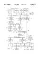
- FIG. 1is a block diagram of one illustrative system that could implement the present invention
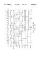
- FIG. 2is a block diagram of the primary and secondary bridges shown in FIG. 1;
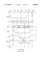
- FIG. 3a-3gare timing diagrams showing events occurring on the buses in the system of FIG. 1;
- FIG. 4is a block diagram corresponding to FIG. 2.
- FIG. 5is a block diagram of one implementation of the present invention.
- a computer system 10which may use features of the invention, according to one embodiment.
- the systemincludes multiple processors 11, 12, 13 and 14 in this example, although the improvements may be used in a single processor environment.
- the processorsare of the type manufactured and sold by Intel Corporation under the trade name "Pentium Pro," although the processors are also referred to as "P6" devices.
- Pentium Prothe processors are also referred to as "P6" devices.
- the structure and operation of these processors 11, 12, 13, and 14are described in detail in the above-mentioned Intel publications, as well as in numerous other publications.
- the processorsare connected to a processor bus 15 which is generally of the structure specified by the processor specification, in this case a Pentium Pro specification.
- the bus 15operates from the processor clock, so if the processors are 166 MHz or 200 MHz devices, for example, then the bus 15 is operated on some multiple of the base clock rate.
- the main memoryis shown connected to the processor bus 15, and includes a memory controller 16 and DRAM memory 17.
- the processors 11, 12, 13, and 14each have a level-two cache L2 as a separate chip within the same package as the CPU chip itself, and of course the CPU chips have level-one L1 data and instruction caches included on-chip.
- a bridge 18 or 19is provided between the processor bus 15 and a PCI bus 20 or 21.
- Two bridges 18 and 19are shown, although it is understood that many systems would require only one, and other systems may use more than two. In one example, up to four of the bridges may be used. The reason for using more than one bridge is to increase the potential data throughput.
- a PCI busas mentioned above, is a standardized bus structure that is built according to a specification agreed upon by a number of equipment manufacturers so that cards for disk controllers, video controllers, modems, network cards, and the like can be made in a standard configuration, rather than having to be customized for each system manufacturer.
- the primary bridge 18 in this examplecarries traffic for the "legacy" devices such as (E)ISA bus, 8259 interrupt controller, VGA graphics, IDE hard disk controller, etc.
- the secondary bridge 19does not usually incorporate any PC legacy items.
- Peer-to-peer transactionsare allowed between a master and target device on the same PCI bus 20 or 21; these are called “standard" peer-to-peer transactions. Transactions between a master on one PCI bus and a target device on another PCI bus must traverse the processor bus 15, and these are "traversing" transactions; memory and I/O reads and writes are allowed in this case but not locked cycles and some other special events.
- PC legacy devicesare coupled to the PCI bus 20 by an (E)ISA bridge 23 to an EISA/ISA bus 24.
- Attached to the bus 24are components such as a controller 25 (e.g., an 8042) for keyboard and mouse inputs 26, flash ROM 27, NVRAM 28, and a controller 29 for floppy drive 30 and serial/parallel ports 31.
- a video controller 32 for a monitor 33is also connected to the bus 20.
- a network 38is accessed by the adapter 37, and a large number of other stations (computer systems) 39 are coupled to the network.
- transactions on the buses 15, 20, and 21may originate in or be directed to another station or server 39 on the network 38.
- the embodiment of FIG. 1is that of a server, rather than a standalone computer system, but the bridge features can be used as well in a workstation or standalone desktop computer.
- the controllerssuch as 32, 34, and 37 would usually be cards fitted into PCI bus slots on the motherboard. If additional slots are needed, a PCI-to-PCI bridge 40 may be placed on the PCI bus 21 to access another PCI bus 41; this would not provide additional bandwidth, but would allow more adapter cards to be added.
- Various other server resourcescan be connected to the PCI buses 20, 21, and 41, using commercially-available controller cards, such as CD-ROM drives, tape drives, modems, connections to ISDN lines for internet access, etc.
- the processor bus 15contains a number of standard signal or data lines as defined in the specification for the Pentium Pro or P6 processor, mentioned above. In addition, certain special signals are included for the unique operation of the bridges 18 and 19, as will be described.
- the bus 15contains thirty-three address lines 15a, sixty-four data lines 15b, and a number of control lines 15c. Most of the control lines are not material here and will not be referred to; also, data and address signals have parity lines associated with them which will not be treated here.
- control signals of interest hereare described in Appendix A, and include the address strobe ADS#, data ready DRDY#, lock LOCK#, data busy DBSY#, defer DEFER#, request command REQ[4:0]# (five lines), response status RS[2:0]#, etc.
- the PCI bus 20(or 21) also contains a number of standard signal and data lines as defined in the PCI specification.
- This busis a multiplexed address/data type, and contains sixty-four AD lines 20a, eight command/byte-enable lines 20b, and a number of control lines 20c as will be described.
- the definition of the control lines of interest hereis given in Appendix B, including initiator ready IRDY#, lock P -- LOCK#, target ready TRDY#, STOP#, etc.
- PCI arbiter signals 20dalso described in Appendix B, including request REQx#, grant P -- GNTx#, MEMACK#, etc.
- This bridgeincludes an interface circuit 43 serving to acquire data and signals from the processor bus 15 and to drive the processor bus with signals and data according to Appendix A.
- An interface 44serves to drive the PCI bus 20 and to acquire signals and data from the PCI bus according to Appendix B.
- the bridgeis divided into an upstream queue block 45 (US QBLK) and a downstream queue block 46 (DS QBLK).
- US QBLKupstream queue block 45
- DS QBLKdownstream queue block 46
- the bridgeinterfaces on the upstream side with the processor bus 15 which operates at a bus speed related to the processor clock rate which is, for example, 133 MHz, 166 MHz, or 200 MHz for Pentium Pro processors, whereas it interfaces on the downstream side with the PCI bus which operates at 33 or 66 MHz.
- the bridge 18one function of the bridge 18 is that of a buffer between asynchronous buses, and buses which differ in address/data presentation, i.e., the processor bus 15 has separate address and data lines, whereas the PCI bus uses multiplexed address and data lines. To accomplish these translations, all bus transactions are buffered in FIFO's.
- An internal bus 47conveys 1processor bus write transactions or read data from the interface 43 to a downstream delayed completion queue DSDCQ 48 and a RAM 49 for this queue, or to a downstream posted write queue 50 and a RAM 51 for this queue.
- Read requests going downstreamare stored in a downstream delayed request queue DSDRQ 52.
- An arbiter 53monitors all pending downstream posted writes and read requests via valid bits on lines 54 in the downstream queues and schedules which one will be allowed to execute next on the PCI bus according to the read and write ordering rules set forth in the PCI bus specification. Commands to the interface 44 from the arbiter 53 are on lines 55.
- upstream queue block 45The components of upstream queue block 45 are similar to those of the downstream queue block 46, i.e., the bridge 18 is essentially symmetrical for downstream and upstream transactions.
- a memory write transaction initiated by a device on the PCI bus 20is posted to the PCI interface 44 of FIG. 2 and the master device proceeds as if the write had been completed.
- a read requested by a device on the PCI bus 20is not implemented at once by a target device on the processor bus 15, so these reads are again treated as delayed transactions.
- An internal bus 57conveys PCI bus write transactions or read data from the interface 44 to an upstream delayed completion queue USDCQ 58 and a RAM 59 for this queue, or to an upstream posted write queue 60 and a RAM 61 for this queue.
- Read requests going upstreamare stored in an upstream delayed request queue USDRQ 62.
- An arbiter 63monitors all pending upstream posted writes and read requests via valid bits on lines 64 in the upstream queues and schedules which one will be allowed to execute next on the processor bus according to the read and write ordering rules set forth in the PCI bus specification. Commands to the interface 43 from the arbiter 63 are on lines 65.
- Each buffer in a delayed request queuei.e., DSDRQ 52 or USDRQ 62, stores a delayed request that is waiting for execution, and this delayed request consists of a command field, an address field, a write data field (not needed if this is a read request), and a valid bit.
- the upstream USDRQ 62holds requests originating from masters on the PCI bus and directed to targets on the processor bus 15 and has eight buffers (in an example embodiment), corresponding one-to-one with eight buffers in the downstream delayed completion queue DSDCQ 48.
- the downstream delayed request queue DSDRQ 52holds requests originating on the processor bus 15 and directed to targets on the PCI bus 20 and has four buffers, corresponding one-to-one with four buffers in the upstream delayed completion queue USDCQ 58.
- the DSDRQ 52is loaded with a request from the interface 43 via bus 72 and the USDCQ 58.
- the USDRQ 62is loaded from interface 44 via bus 73 and DSDCQ 48.
- the reason for going through the DCQ logicis to check to see if a read request is a repeat of a request previously made.
- a read request from the bus 15is latched into the interface 43 in response to an ADS#, capturing an address, a read command, byte enables, etc.
- This informationis applied to the USDCQ 58 via lines 74, where it is compared with all enqueued prior downstream read requests; if it is a duplicate, this new request is discarded if the data is not available to satisfy the request, but if it is not a duplicate, the information is forwarded to the DSDRQ 52 via bus 72.
- the same mechanismis used for upstream read requests; information defining the request is latched into interface 44 from bus 20, forwarded to DSDCQ 48 via lines 75, and if not a duplicate of an enqueued request it is forwarded to USDRQ 62 via bus 73.
- the delayed completion queueseach include a control block 48 or 58 and a dual port RAM 49 or 59.
- Each buffer in a DCQstores completion status and read data for one delayed request.
- the first stepis to check within the DCQ 48 or 58 to see if a buffer for this same request has already been allocated. The address and the commands and byte enables are checked against the eight buffers in DCQ 48 or 58. If not a match, then a buffer is allocated (if one is available) the request is delayed (or deferred for the bus 15), and the request is forwarded to the DRQ 52 or 62 in the opposite side via lines 72 or 73.
- This requestis run on the opposite bus, under control of the arbiter 53 or 63, and the completion status and data are forwarded back to the DCQ 48 or 58 via bus 47 or 57.
- this bufferis not valid until ordering rules are satisfied; e.g., a write cannot be completed until previous reads are completed.
- a delayable request"matches" a DCQ buffer and the requested data is valid, then the request cycle is ready for immediate completion.
- the downstream DCQ 48stores status/read data for PCI-to-host delayed requests
- the upstream DCQ 58stores status/read data for Host-to-PCI delayed or deferred requests.
- the upstream and downstream operationis slightly different in this regard.
- the bridge control circuitrycauses prefetch of data into the DSDCQ buffers 48 on behalf of the master, attempting to stream data with zero wait states after the delayed request completes.
- DSDCQ buffersare kept coherent with the host bus 15 via snooping, which allows the buffers to be discarded as seldom as possible. Requests going the other direction are not subjected to prefetching, however, since many PCI memory regions have "read side effects" (e.g., stacks and FIFO's) the bridge never prefetches data into these buffers on behalf of the master, and USDCQ buffers are flushed as soon as their associated deferred reply completes.
- read side effectse.g., stacks and FIFO's
- the posted write queueseach contain a control block 50 or 60 and a dual port RAM memory 51 or 61, with each one of the buffers in these RAMs storing command and data for one write. Only memory writes are posted, i.e., writes to I/O space are not posted. Because memory writes flow through dedicated queues within the bridge, they cannot blocked by delayed requests that precede them; this is a requirement of the PCI specification.
- Each of the four buffers in DSPWQ 50, 51stores 32-Bytes of data plus commands for a host-to-PCI write; this is a cache line--the bridge might receive a cacheline-sized write if the system has a PCI video card that supports the p.sup. ⁇ USWC memory type.
- the four buffers in the DSPWQ 50, 51provide a total data storage of 128-Bytes.
- the arbiters 53 and 63control event ordering in the QBLKs 45 and 46. These arbiters make certain that any transaction in the DRQ 52 or 62 is not attempted until posted writes that preceded it are flushed, and that no datum in a DCQ is marked valid until posted writes that arrived in the QBLK ahead of it are flushed.
- the data and control signal protocol on the bus 15is defined by the processors 11-14, which in the example are Intel "Pentium Pro" devices.
- the processors 11-14have a bus interface circuit within each chip which provides the bus arbitration and snoop functions for the bus 15.
- a P6 bus cycleincludes six phases: an arbitration phase, a request phase, an error phase, a snoop phase, a response phase, and a data phase.
- a simple read cycle where data is immediately availablei.e., a read from main memory 17 is illustrated in FIG. 3a.
- This readis initiated by first acquiring the bus; a bus request is asserted on the BREQn# line during T1; if no other processors having a higher priority (using a rotating scheme) assert their BREQn#, a grant is assumed and an address strobe signal ADS# is asserted in T2 for one clock only.
- the address, byte enables and command signalsare asserted on the A# lines, beginning at the same time as ADS#, and continuing during two cycles, T3 and T4, i.e., the asserted information is multiplexed onto the A# lines in two cycles. During the first of these, the address is applied, and during the second, the byte enables and the commands are applied.
- the error phaseis a parity check on the address bits, and if a parity error is detected an AERR# signal is asserted during T5, and the transaction aborts.
- the snoop phaseoccurs during T7; if the address asserted during T3 matches the tag of any of the L2 cache lines and is modified, or any other resource on bus 15 for which coherency is maintained, a HITM# signal is asserted during T7, and a writeback must be executed before the transaction proceeds. That is, if the processor 11 attempts to read a location in main memory 17 which is cached and modified at that time in the L2 cache of processor 12, the read is not allowed to proceed until a writeback of the line from L2 of processor 12 to memory 17 is completed, so the read is delayed.
- the transactionenters the response phase during T9.
- a response codeis asserted during T9; the response code indicates "normal data,” “retry,” “deferred,” etc., depending on when the data is going to be available in response to the read request.
- the response codeis "normal data” and the data itself is asserted on data lines D[63:0]# during T9 and T12 (the data phase); usually a read request to main memory is for a cache line, 128-bytes, so the cache line data appears on the data lines during two cycles, 64-bytes each cycle, as shown.
- the data bus busy line DBSY#is sampled before data is asserted, and if free then the responding agent asserts DBSY# itself during T9-T11 to hold the bus, and asserts data ready on the DRDY# line to indicate that valid data is being applied to the data lines.
- FIG. 3bA simple write transaction on the P6 bus 15 is illustrated in FIG. 3b.
- the initiatorasserts ADS# and asserts the REQa0# (command and B/E's).
- TRDY#is asserted three clocks later in T6.
- TRDY#is active and DBSY# is inactive in T8, so data transfer can begin in T9; DRDY# is asserted at this time.
- the initiatordrives data onto the data bus D[63:0]# during T9.
- FIG. 3cA burst or full-speed read transaction is illustrated in FIG. 3c.
- Back-to-back read datatransfers from the same agent with no wait states. Note that the request for transaction-4 is being driven onto the bus while data for transaction-1 is just completing in T10, illustrating the overlapping of several transactions. DBSY# is asserted for transaction-1 in T7 and remains asserted until T10. Snoop results indicate no implicit writeback data transfers so TRDY# is not asserted.
- TRDY# for transaction-2can be driven the cycle after RS[2:0]# is driven.
- the targetsamples TRDY# active and DBSY# inactive and accepts data transfer starting in T12. Because the snoop results for transaction-2 have been observed in T9, the target is free to drive the response in T12.
- a deferred read transactionis illustrated in FIG. 3e. This is a split transaction, meaning the request is put out on the bus, then at some time later the target initiates a reply to complete the transaction, while other transactions occur on the bus in the intervening time.
- Agentsuse the deferred response mechanism of the P6 bus when an operation has significantly greater latency than the normal in-order response.
- an agentcan assert Defer Enable DEN# to indicate if the transaction can be given a deferred response. If DEN# is inactive, the transaction cannot receive a deferred response; some transactions must always be issued with DEN# inactive, e.g., bus-locked transactions, deferred replies, writebacks.
- DEN#When DEN# is inactive, the transaction may be completed in-order or it may be retried, but it cannot be deferred.
- a deferred transactionis signalled by asserting DEFER# during the snoop phase followed by a deferred response in the response phase.
- the response agentOn a deferred response, the response agent must latch the deferred ID, DID[7:0]#, issued during the request phase, and after the response agent completes the original request, it must issue a matching deferred-reply bus transaction, using the deferred ID as the address in the reply transaction's request phase.
- the deferred IDis eight bits transferred on pins Ab[23:16] in the second clock of the original transaction's request phase.
- FIG. 3fA read transaction on the PCI bus 20 (or 21) is illustrated in FIG. 3f. It is assumed that the bus master has already arbitrated for and been granted access to the bus. The bus master must then wait for the bus to become idle, which is done by sampling FRAME# and IRDY# on the rising edge of each clock (along with GNT#); when both are sampled deasserted, the bus is idle and a transaction can be initiated by the bus master. At start of clock T1, the initiator asserts FRAME#, indicating that the transaction has begun and that a valid start address and command are on the bus. FRAME# must remain asserted until the initiator is ready to complete the last data phase.
- the initiatorWhen the initiator asserts FRAME#, it also drives the start address onto the AD bus and the transaction type onto the Command/Byte Enable lines, C/BE[3:0]#.
- a turn-around cyclei.e., a dead cycle
- the initiatorceases driving the AD bus, allowing the target to take control of the AD bus to drive the first requested data item back to the initiator.
- the initiatorceases to drive the command onto the C/BE lines and uses them to indicate the bytes to be transferred in the currently addressed doubleword (typically, all bytes are asserted during a read).
- the initiatoralso asserts IRDY# during T2 to indicate it is ready to receive the first data item from the target.
- the initiatorasserts IRDY# and desserts FRAME# to indicate that it is ready to complete the last data phase (T5 in FIG. 3f).
- the targetasserts DEVSEL# to indicate that it recognized its address and will participate in the transaction, and begins to drive the first data item onto the AD bus while it asserts TRDY# to indicate the presence of the requested data.
- TRDY# asserted in T3it reads the first data item from the bus.
- the initiatorkeeps IRDY# asserted upon entry into the second data phase in T4, and does not deassert FRAME#, indicating it is ready to accept the second data item.
- the targetlatches the start address into an address counter, and increments this address to generate the subsequent addresses.
- the processor bus 15is connected through the processor bus interface 43, the upstream queue block 45, the downstream queue block 46 and the PCI interface 44 to the PCI bus 20.
- the processor bus interface 43includes a processor bus initiator 60 and a processor bus target 62.
- the target 62is capable of two-way communications with the upstream queue block 45.
- the PCI initiator 66communicates with the downstream queue block 46.
- the PCI initiator 66 and PCI target 64are part of the PCI interface 44.
- the PCI initiator 66 and processor target 62are shown to better explain the relationship with certain transactions on the PCI bus 20. Also depicted is a configuration module 68 which may be implemented as part of the PCI bus interface 44. It may include configuration, diagnostic and/or memory mapped registers.
- the PCI initiator 66may initiate a transaction which originally was run on the processor bus 15 and which is transferred to the PCI initiator 66 from the processor bus target 62. As indicated in FIG. 5, the processor bus target 62 may receive a request for a transaction and ultimately provide a response to the processor bus 15. The processor target 62 sends the request through the queue block 45 to the PCI initiator 66. The PCI initiator 66 then runs the transaction on the line 70. The transaction on the line 70 passes through a multiplexor 72 to a bi-directional buffer including the buffers 74 and 76 and out to the PCI bus 20. The same transaction may be bidirectionally routed through the amplifier 76 to a second multiplexor 78.
- a new transaction from the initiator 66would be passed directly through the second multiplexor 78 to the configuration module 68 via the path 79.
- One instance where this would occurwould be when the configuration module 68 was the ultimate target of the transaction being run by the PCI initiator 66.
- the transactionmay then also be run on the PCI bus 20.
- the multiplexor 72is controlled by a signal on the line 84.
- the multiplexor 72may be switched by a signal on the line 84 to allow either the PCI initiator 66 or the configuration module 68 via the line 86, to control the PCI bus 20.
- the multiplexor 78is controlled by a signal issued from the PCI initiator 66 over the line 88.
- the multiplexor 78may be operable to reject a bidirectional signal from the buffer 76 and to simply pass the original PCI initiator transaction from the line 70 directly to the configuration module 68. In this way, a transaction initiated from the PCI initiator 66 may be run on the PCI bus 20. However, the transaction is also directed straight to the configuration module 68 when it is the intended target.
- the configuration module 68may then respond with data over the lines 86 and 98 to the P6 target 62. Ultimately, this information may get back to the P6 bus 15. In some instances, the data may also be provided, via line 86, to the PCI bus 20 through the multiplexor 72.
- the PCI busWhen the PCI bus is in a hang or other error condition, there may be critical information stored in the module 68 which could not be accessed via the PCI bus 20. In this case, direct access to the configuration module 68, without using the PCI bus 20, allows critical information to be obtained.
- the information stored in the module 68could include a listing of recent transactions including the initiator, the target and the type of command that was involved. This information is useful in determining the cause of the hang condition on the PCI bus 20. It may be utilized to attempt to diagnose the problem and in some cases to even correct the problem without requiring a system shut down.
- transactions from the PCI initiator 66could be run both on the bus 20 and directly through the module 68 with the return path controlled by the module 68.
- the module 68could switch the multiplexer 96 (by a path not shown) when the module 68 claims the cycle.
- the PCI initiator 66When the transaction, which is actually being shunted directly to the configuration module 68, is run on the PCI bus by the PCI initiator 66, it may be necessary to mask the ID select signal which would identify the particular target device. This ID select signal would correspond to a multiplexed address in normal PCI terminology.
- the initiatorOn the PCI bus 20 during configuration cycles, the initiator asserts one address line that corresponds to the target of the configuration cycle. The signal identifies the target device and therefore initiates a response by the target device. Since it would be undesirable for any target to respond (since the configuration module 68 is being addressed directly), this signal from the initiator 66 is masked by the logic gate 94.
- the logic gate 94When the logic gate 94 receives a signal on the line 90 indicating that a direct cycle to the configuration module 68 is being run, the master ID select signal on the line 92 is blocked. This makes all other devices ignore the configuration access that was run on the bus 20. Thus, no target responds to the PCI bus transaction.
- the arbiters 53, 63keep the transactions in sync with one another. During normal transactions, the master ID select signal would issue on the bus 20.
- the bidirectional signal from the buffer 76may, under certain circumstances, be passed by the multiplexor 96 to the processor target device 62. Control over the switching operation of the multiplexor 96 may also be obtained via the line 90. Similarly, data and control signals outputted from the configuration module 68 may be shunted directly to upstream queue block 45 and the processor target 62 via the line 98 when the multiplexor 96 is in the appropriate configuration. The signal on the line 90 used to the control the ID select signal also controls the multiplexor 78 and the multiplexor 96.
- the configuration module 68 and bridge 18 or 19may be implemented on one semiconductor die. Alternatively, they may be separate, integrated circuits.
- the configuration module 68could include a FIFO buffer which stores information about transactions that have occurred previously.
- the buffermay be a given number of spaces deep and that given number of transactions are stored such that the last several transactions are stored in a shorthand format in the buffer. If the bus hangs, information about the last several transactions can be analyzed. Generally, the failure condition would be detected by a watch dog timer time out indicating that no valid data transfer happened on the bus for a predetermined amount of time (e.g., 2 18 clock cycles). The transaction could then be terminated by asserting STOP# followed by target abort, taking the device off of the bus. A reset could be utilized to see if the bus hang condition had been remedied.
- the use of the internal direct pathalso may eliminate the worst case reflections.
- Each device on the bus 20, 21 downstream from a bridge 18, 19, shown in FIG. 1receives a signal and a reflected signal from the end of the bus 20, 21 farthest away from the bridge.
- the delay from the bridge back to the bridgeis the longest delay.
- the signal qualityis poorest for signals from the bridge 18, 19 back to the same bridge 18, 19.
- the internal direct pathmay eliminate these worst case reflections. For this purpose, it is advantageous to use the internal direct path for configuration and memory transactions.
- ADS#--Address Strobeasserted to defines the beginning of the Request Phase.
- the REQa[4:0]# and Aa[35:3]# signalsare valid in the clock that ADS# is asserted (the "a") clock).
- the REQb[4:0]# and Ab[35:3]# signalsare valid in the next clock after ADS# was asserted (the "b") clock).
- A[35.3]#--Address signalsconveying information during both clocks of two-clock request phase.
- Aa[35:3]#are signals during first clock and Ab[35:3]# are signals during second clock.
- Aa[35:3]#convey address, and Ab[35:3]# convey cycle-type, byte enable, deferred ID, etc.
- D[63:0]#--System Datasignals--carry the data for a transaction during the data phase.
- REQ[4:0]#--Request command signalsasserted during both clocks of the request phase, indicating type of transaction being requested and info about that transaction.
- RS[2:0]#--Response status signalsdriven by the target during the response phase, indicate how current transaction will be processed.
- Valid responsesinclude: Normal with or without data; Idle; Retry; Defer; Implicit Writeback.
- DBSY#--Data bus busy signalasserted by the agent driving the data on D[63:0]# to indicate a multi-clock data phase. Asserted on first clock that data may be driven, deasserted when the data bus is no longer needed.
- DEFER#--Defer signalused by target to indicate to the agent issuing the transaction that it may not be completed in order.
- An active DEFER#means that the associated transaction will complete with a DEFER REPLY or a RETRY response.
- DRDY#--Date ready signaldriven in same clock as the D[63:0]# signals and indicates that the data is valid and may be sampled.
- TRDY#--Target ready signaldriven by the target for write transactions to indicate that target is ready to accept the current data for a write or writeback.
- HIT#--Cache hit signal for snoopingalong with HITM# determine results of snoop phase.
- HITM#is the cache hit to modified signal.
- GNTn#--Arbiter grant signal to masterindicating initiator is granted the bus.
- LOCK#--Bus lock signalasserted from the request phase of the first transaction through the response phase of the final transaction. No other bus masters may issue transactions during a bus lock. Locked cycle may be stopped on the first transaction if DEFER# is asserted, or by error signals.
- AD[31:0]--Address/Data(with AD[63:32] for 64-bit bus)conveys the address for a read or write request, then Used to transfer data.
- DEVSEL#--Device Select--indicates driving devicehas decoded its address as the target of the current access. As an input, it indicates whether any device on the bus has been selected.
- STOP#--Targetis requesting the master to stop the current bus transaction. Aborts.
- REQ#--Request--arbitration signalasserted by an initiator when requesting the bus.
- GNT#--Grant--signal from arbiter to agent in response to REQ#indicating that bus has been granted to agent--one of six signals with one going to each device.
- LOCK#--Atomic operationmay require multiple transactions to complete, asserted when transaction must be completed before any other transaction can be initiated. Only supported going downstream.
Landscapes
- Engineering & Computer Science (AREA)
- Theoretical Computer Science (AREA)
- General Engineering & Computer Science (AREA)
- Quality & Reliability (AREA)
- Physics & Mathematics (AREA)
- General Physics & Mathematics (AREA)
- Computer Hardware Design (AREA)
- Bus Control (AREA)
- Debugging And Monitoring (AREA)
- Test And Diagnosis Of Digital Computers (AREA)
Abstract
Description
Claims (12)
Priority Applications (2)
| Application Number | Priority Date | Filing Date | Title |
|---|---|---|---|
| US08/882,504US6098137A (en) | 1996-06-05 | 1997-06-25 | Fault tolerant computer system |
| US09/534,249US6321286B1 (en) | 1996-06-05 | 2000-03-23 | Fault tolerant computer system |
Applications Claiming Priority (2)
| Application Number | Priority Date | Filing Date | Title |
|---|---|---|---|
| US08/658,750US6032271A (en) | 1996-06-05 | 1996-06-05 | Method and apparatus for identifying faulty devices in a computer system |
| US08/882,504US6098137A (en) | 1996-06-05 | 1997-06-25 | Fault tolerant computer system |
Related Parent Applications (1)
| Application Number | Title | Priority Date | Filing Date |
|---|---|---|---|
| US08/658,750Continuation-In-PartUS6032271A (en) | 1996-06-05 | 1996-06-05 | Method and apparatus for identifying faulty devices in a computer system |
Related Child Applications (1)
| Application Number | Title | Priority Date | Filing Date |
|---|---|---|---|
| US09/534,249ContinuationUS6321286B1 (en) | 1996-06-05 | 2000-03-23 | Fault tolerant computer system |
Publications (1)
| Publication Number | Publication Date |
|---|---|
| US6098137Atrue US6098137A (en) | 2000-08-01 |
Family
ID=24642524
Family Applications (3)
| Application Number | Title | Priority Date | Filing Date |
|---|---|---|---|
| US08/658,750Expired - LifetimeUS6032271A (en) | 1996-06-05 | 1996-06-05 | Method and apparatus for identifying faulty devices in a computer system |
| US08/882,504Expired - LifetimeUS6098137A (en) | 1996-06-05 | 1997-06-25 | Fault tolerant computer system |
| US09/534,249Expired - Fee RelatedUS6321286B1 (en) | 1996-06-05 | 2000-03-23 | Fault tolerant computer system |
Family Applications Before (1)
| Application Number | Title | Priority Date | Filing Date |
|---|---|---|---|
| US08/658,750Expired - LifetimeUS6032271A (en) | 1996-06-05 | 1996-06-05 | Method and apparatus for identifying faulty devices in a computer system |
Family Applications After (1)
| Application Number | Title | Priority Date | Filing Date |
|---|---|---|---|
| US09/534,249Expired - Fee RelatedUS6321286B1 (en) | 1996-06-05 | 2000-03-23 | Fault tolerant computer system |
Country Status (5)
| Country | Link |
|---|---|
| US (3) | US6032271A (en) |
| EP (1) | EP0820012B1 (en) |
| JP (1) | JPH10116208A (en) |
| DE (1) | DE69721654T2 (en) |
| TW (1) | TW378292B (en) |
Cited By (30)
| Publication number | Priority date | Publication date | Assignee | Title |
|---|---|---|---|---|
| US20010032300A1 (en)* | 2000-04-14 | 2001-10-18 | Thomas Olson | Method and apparatus for storing transactional information in persistent memory |
| US6321286B1 (en)* | 1996-06-05 | 2001-11-20 | Compaq Computer Corporation | Fault tolerant computer system |
| US20030061424A1 (en)* | 2001-09-26 | 2003-03-27 | Leete Brian A. | Method and apparatus for dual queue head processing of interrupt endpoints |
| US6633996B1 (en) | 2000-04-13 | 2003-10-14 | Stratus Technologies Bermuda Ltd. | Fault-tolerant maintenance bus architecture |
| US6636928B1 (en)* | 2000-02-18 | 2003-10-21 | Hewlett-Packard Development Company, L.P. | Write posting with global ordering in multi-path systems |
| US6687851B1 (en) | 2000-04-13 | 2004-02-03 | Stratus Technologies Bermuda Ltd. | Method and system for upgrading fault-tolerant systems |
| US6691257B1 (en) | 2000-04-13 | 2004-02-10 | Stratus Technologies Bermuda Ltd. | Fault-tolerant maintenance bus protocol and method for using the same |
| US6708283B1 (en) | 2000-04-13 | 2004-03-16 | Stratus Technologies, Bermuda Ltd. | System and method for operating a system with redundant peripheral bus controllers |
| US6735715B1 (en) | 2000-04-13 | 2004-05-11 | Stratus Technologies Bermuda Ltd. | System and method for operating a SCSI bus with redundant SCSI adaptors |
| US20040139259A1 (en)* | 2003-01-15 | 2004-07-15 | Mantey Paul J. | Systems and methods for accessing bus-mastered system resources |
| US6766479B2 (en) | 2001-02-28 | 2004-07-20 | Stratus Technologies Bermuda, Ltd. | Apparatus and methods for identifying bus protocol violations |
| US6771664B1 (en) | 1999-12-28 | 2004-08-03 | Intel Corporation | Transaction scheduling for a bus system in a multiple speed environment |
| US6802022B1 (en) | 2000-04-14 | 2004-10-05 | Stratus Technologies Bermuda Ltd. | Maintenance of consistent, redundant mass storage images |
| US6813251B1 (en)* | 1999-07-27 | 2004-11-02 | Intel Corporation | Split Transaction protocol for a bus system |
| US6820213B1 (en) | 2000-04-13 | 2004-11-16 | Stratus Technologies Bermuda, Ltd. | Fault-tolerant computer system with voter delay buffer |
| US6862689B2 (en) | 2001-04-12 | 2005-03-01 | Stratus Technologies Bermuda Ltd. | Method and apparatus for managing session information |
| US6886171B2 (en) | 2001-02-20 | 2005-04-26 | Stratus Technologies Bermuda Ltd. | Caching for I/O virtual address translation and validation using device drivers |
| US20050172169A1 (en)* | 1999-02-24 | 2005-08-04 | Tomoki Sekiguchi | Computer system and fault processing method in computer system |
| US6996750B2 (en) | 2001-05-31 | 2006-02-07 | Stratus Technologies Bermuda Ltd. | Methods and apparatus for computer bus error termination |
| US20060117300A1 (en)* | 2004-11-23 | 2006-06-01 | Puthukattukaran James J | Tracking modified pages on a computer system |
| US7065672B2 (en) | 2001-03-28 | 2006-06-20 | Stratus Technologies Bermuda Ltd. | Apparatus and methods for fault-tolerant computing using a switching fabric |
| US20060143528A1 (en)* | 2004-12-27 | 2006-06-29 | Stratus Technologies Bermuda Ltd | Systems and methods for checkpointing |
| US20070028144A1 (en)* | 2005-07-29 | 2007-02-01 | Stratus Technologies Bermuda Ltd. | Systems and methods for checkpointing |
| US20070038891A1 (en)* | 2005-08-12 | 2007-02-15 | Stratus Technologies Bermuda Ltd. | Hardware checkpointing system |
| US9251002B2 (en) | 2013-01-15 | 2016-02-02 | Stratus Technologies Bermuda Ltd. | System and method for writing checkpointing data |
| US9588844B2 (en) | 2013-12-30 | 2017-03-07 | Stratus Technologies Bermuda Ltd. | Checkpointing systems and methods using data forwarding |
| US9652338B2 (en) | 2013-12-30 | 2017-05-16 | Stratus Technologies Bermuda Ltd. | Dynamic checkpointing systems and methods |
| US9760442B2 (en) | 2013-12-30 | 2017-09-12 | Stratus Technologies Bermuda Ltd. | Method of delaying checkpoints by inspecting network packets |
| US20180074875A1 (en)* | 2016-09-15 | 2018-03-15 | International Business Machines Corporation | Hang detection and recovery |
| CN114153637A (en)* | 2020-08-17 | 2022-03-08 | 昆达电脑科技(昆山)有限公司 | server system |
Families Citing this family (54)
| Publication number | Priority date | Publication date | Assignee | Title |
|---|---|---|---|---|
| US6134665A (en)* | 1998-01-20 | 2000-10-17 | Digital Equipment Corporation | Computer with remote wake up and transmission of a status packet when the computer fails a self test |
| US6226762B1 (en)* | 1998-04-20 | 2001-05-01 | National Instruments Corporation | System and method for providing delayed start-up of an activity monitor in a distributed I/O system |
| US6138247A (en)* | 1998-05-14 | 2000-10-24 | Motorola, Inc. | Method for switching between multiple system processors |
| US6463550B1 (en) | 1998-06-04 | 2002-10-08 | Compaq Information Technologies Group, L.P. | Computer system implementing fault detection and isolation using unique identification codes stored in non-volatile memory |
| US6141757A (en)* | 1998-06-22 | 2000-10-31 | Motorola, Inc. | Secure computer with bus monitoring system and methods |
| JP4132322B2 (en)* | 1998-12-16 | 2008-08-13 | 株式会社日立製作所 | Storage control device and control method thereof |
| JP4371466B2 (en)* | 1999-04-15 | 2009-11-25 | 株式会社東芝 | Computer system and method for controlling I/O device thereof |
| FI107207B (en)* | 1999-04-28 | 2001-06-15 | Nokia Networks Oy | Method, system, and device for identifying a faulty unit |
| US6453429B1 (en)* | 1999-04-29 | 2002-09-17 | International Business Machines Corporation | Method and apparatus for bus hang detection and identification of errant agent for fail safe access to trapped error information |
| FI19991735A7 (en)* | 1999-08-16 | 2001-02-17 | Nokia Corp | Method and device for improving the reliability of a computer system |
| US7266728B1 (en)* | 1999-10-01 | 2007-09-04 | Stmicroelectronics Ltd. | Circuit for monitoring information on an interconnect |
| US7260745B1 (en)* | 1999-10-01 | 2007-08-21 | Stmicroelectronics Ltd. | Detection of information on an interconnect |
| JP2001222385A (en)* | 2000-02-10 | 2001-08-17 | Hitachi Ltd | Storage device and information processing system |
| TW525053B (en)* | 2000-03-29 | 2003-03-21 | Mitac Int Corp | Apparatus of PCI bus cycle single step interrupt debug card and its method |
| US7168032B2 (en)* | 2000-12-15 | 2007-01-23 | Intel Corporation | Data synchronization for a test access port |
| US6948010B2 (en) | 2000-12-20 | 2005-09-20 | Stratus Technologies Bermuda Ltd. | Method and apparatus for efficiently moving portions of a memory block |
| US6769078B2 (en)* | 2001-02-08 | 2004-07-27 | International Business Machines Corporation | Method for isolating an I2C bus fault using self bus switching device |
| US20020184576A1 (en)* | 2001-03-29 | 2002-12-05 | International Business Machines Corporation | Method and apparatus for isolating failing hardware in a PCI recoverable error |
| US6928583B2 (en)* | 2001-04-11 | 2005-08-09 | Stratus Technologies Bermuda Ltd. | Apparatus and method for two computing elements in a fault-tolerant server to execute instructions in lockstep |
| JP2002312199A (en)* | 2001-04-13 | 2002-10-25 | Mitsubishi Electric Corp | Anomaly detection electronic device, anomaly detection method, anomaly detection electronic device system, anomaly detection program, and computer-readable recording medium recording anomaly detection program |
| US6701403B2 (en)* | 2001-10-01 | 2004-03-02 | International Business Machines Corporation | Service processor access of non-volatile memory |
| US20030101310A1 (en)* | 2001-11-29 | 2003-05-29 | Granato Jack L. | Using a PC for testing devices |
| US6938188B1 (en)* | 2002-01-29 | 2005-08-30 | Advanced Digital Information Corporation | Method for verifying functional integrity of computer hardware, particularly data storage devices |
| US20030191978A1 (en)* | 2002-04-04 | 2003-10-09 | International Business Machines Corporation | Multiple fault location in a series of devices |
| US6971049B2 (en)* | 2002-05-23 | 2005-11-29 | International Business Machines Corporation | Method and apparatus for detecting and isolating failures in equipment connected to a data bus |
| US6832286B2 (en)* | 2002-06-25 | 2004-12-14 | Hewlett-Packard Development Company, L.P. | Memory auto-precharge |
| US6944796B2 (en)* | 2002-06-27 | 2005-09-13 | Intel Corporation | Method and system to implement a system event log for system manageability |
| US7069477B2 (en)* | 2002-10-30 | 2006-06-27 | International Business Machines Corporation | Methods and arrangements to enhance a bus |
| US7080288B2 (en)* | 2003-04-28 | 2006-07-18 | International Business Machines Corporation | Method and apparatus for interface failure survivability using error correction |
| US7134052B2 (en)* | 2003-05-15 | 2006-11-07 | International Business Machines Corporation | Autonomic recovery from hardware errors in an input/output fabric |
| KR100503796B1 (en)* | 2003-06-05 | 2005-07-26 | 삼성전자주식회사 | Method and apparatus detecting an error of an access wait signal |
| US7082488B2 (en)* | 2003-06-12 | 2006-07-25 | Hewlett-Packard Development Company, L.P. | System and method for presence detect and reset of a device coupled to an inter-integrated circuit router |
| US7206973B2 (en)* | 2003-12-11 | 2007-04-17 | Lsi Logic Corporation | PCI validation |
| US20050193246A1 (en)* | 2004-02-19 | 2005-09-01 | Marconi Communications, Inc. | Method, apparatus and software for preventing switch failures in the presence of faults |
| TW200537305A (en)* | 2004-05-04 | 2005-11-16 | Quanta Comp Inc | Communication system, transmission device and the control method thereof |
| US7428665B2 (en)* | 2004-11-12 | 2008-09-23 | Lsi Corporation | Methods and structure for detection and handling of catastrophic SCSI errors |
| US7095217B1 (en)* | 2005-03-31 | 2006-08-22 | O2Micro International Limited | Method circuitry and electronic device for controlling a variable output dc power source |
| US7478286B2 (en)* | 2005-04-08 | 2009-01-13 | Linear Technology Corporation | Circuit and method of detecting and resolving stuck I2C buses |
| JP2007094706A (en)* | 2005-09-28 | 2007-04-12 | Konica Minolta Business Technologies Inc | Data processor, system and method for coping with cable connection abnormality |
| US20080148104A1 (en)* | 2006-09-01 | 2008-06-19 | Brinkman Michael G | Detecting an Agent Generating a Parity Error on a PCI-Compatible Bus |
| US8006122B2 (en)* | 2007-01-10 | 2011-08-23 | International Business Machines Corporation | Methods, systems, and computer products for detection of and policy directed resolution of signaling sympathy sickness in a multisystem cluster |
| TWI403920B (en)* | 2008-03-31 | 2013-08-01 | Aten Int Co Ltd | Kvm switch and method capable of providing edid of display for computer coupled thereto |
| US9077628B2 (en)* | 2008-05-15 | 2015-07-07 | Hewlett-Packard Development Company, L.P. | Network device having a normal operational configuration and fail-safe configuration and method of operating the same |
| JP5539080B2 (en)* | 2010-07-15 | 2014-07-02 | キヤノン株式会社 | Information processing apparatus, information processing system, information processing apparatus control method, communication state confirmation method, and program |
| CN102955718B (en)* | 2011-08-17 | 2016-02-24 | 赛恩倍吉科技顾问(深圳)有限公司 | Server protection system |
| CN102628921B (en)* | 2012-03-01 | 2014-12-03 | 华为技术有限公司 | Integrated circuit and method for monitoring bus state in integrated circuit |
| JP2014095994A (en)* | 2012-11-08 | 2014-05-22 | Azbil Corp | Input/output equipment, system and device |
| US9267965B2 (en)* | 2013-11-19 | 2016-02-23 | Advantest Corporation | Flexible test site synchronization |
| US9830287B2 (en) | 2015-02-24 | 2017-11-28 | Red Hat Israel, Ltd. | Determination of a device function asserting a detected spurious interrupt |
| EP3279796B1 (en)* | 2016-08-02 | 2020-07-15 | NXP USA, Inc. | Resource access management component and method therefor |
| CN110474686B (en)* | 2018-05-11 | 2022-09-16 | 佛山市顺德区顺达电脑厂有限公司 | Network switching device and its operation method |
| CN109491951B (en)* | 2018-09-28 | 2022-05-10 | 超聚变数字技术有限公司 | Data configuration method and computing equipment |
| CN112306781B (en)* | 2020-11-20 | 2022-08-19 | 新华三大数据技术有限公司 | Thread fault processing method, device, medium and equipment |
| US12367123B2 (en)* | 2023-12-06 | 2025-07-22 | Nxp B.V. | Method and system to delay a response associated with a bus transaction that is transmitted to a bus master to perform fault testing |
Citations (17)
| Publication number | Priority date | Publication date | Assignee | Title |
|---|---|---|---|---|
| US4597084A (en)* | 1981-10-01 | 1986-06-24 | Stratus Computer, Inc. | Computer memory apparatus |
| US4953074A (en)* | 1987-07-08 | 1990-08-28 | Hitachi, Ltd. | Function-distributed control apparatus |
| US5289589A (en)* | 1990-09-10 | 1994-02-22 | International Business Machines Corporation | Automated storage library having redundant SCSI bus system |
| US5293586A (en)* | 1988-09-30 | 1994-03-08 | Hitachi, Ltd. | Data processing system for development of outline fonts |
| US5404465A (en)* | 1992-03-18 | 1995-04-04 | Aeg Transportation Systems, Inc. | Method and apparatus for monitoring and switching over to a back-up bus in a redundant trainline monitor system |
| US5471482A (en)* | 1994-04-05 | 1995-11-28 | Unisys Corporation | VLSI embedded RAM test |
| US5568437A (en)* | 1995-06-20 | 1996-10-22 | Vlsi Technology, Inc. | Built-in self test for integrated circuits having read/write memory |
| US5581482A (en)* | 1994-04-26 | 1996-12-03 | Unisys Corporation | Performance monitor for digital computer system |
| US5737338A (en)* | 1993-07-19 | 1998-04-07 | Fujitsu Limited | ATM exchange and method of testing same |
| US5754804A (en)* | 1996-01-30 | 1998-05-19 | International Business Machines Corporation | Method and system for managing system bus communications in a data processing system |
| US5771359A (en)* | 1995-10-13 | 1998-06-23 | Compaq Computer Corporation | Bridge having a data buffer for each bus master |
| US5784558A (en)* | 1996-04-26 | 1998-07-21 | Integrated Network Corporation | Method and apparatus for testing of extended ISDN BRI service |
| US5809021A (en)* | 1994-04-15 | 1998-09-15 | Dsc Communications Corporation | Multi-service switch for a telecommunications network |
| US5812816A (en)* | 1995-06-02 | 1998-09-22 | Sun Microsystems, Inc. | System and method for transferring data between memories of different types occupying a single real address space using a dedicated memory transfer bus |
| US5838899A (en)* | 1994-09-20 | 1998-11-17 | Stratus Computer | Digital data processing methods and apparatus for fault isolation |
| US5838931A (en)* | 1994-12-08 | 1998-11-17 | Intel Corporation | Method and apparatus for enabling a processor to access an external component through a private bus or a shared bus |
| US5857116A (en)* | 1995-10-27 | 1999-01-05 | Compaq Computer Corporation | Circuit for disabling an address masking control signal when a microprocessor is in a system management mode |
Family Cites Families (54)
| Publication number | Priority date | Publication date | Assignee | Title |
|---|---|---|---|---|
| US3810120A (en)* | 1971-02-12 | 1974-05-07 | Honeywell Inf Systems | Automatic deactivation device |
| US4047157A (en)* | 1974-02-01 | 1977-09-06 | Digital Equipment Corporation | Secondary storage facility for data processing |
| US4145734A (en)* | 1975-04-22 | 1979-03-20 | Compagnie Honeywell Bull (Societe Anonyme) | Method and apparatus for implementing the test of computer functional units |
| FR2319264A1 (en)* | 1975-07-22 | 1977-02-18 | Labo Cent Telecommunicat | PERFECTED CONTROL SYSTEM OF SWITCHING EQUIPMENT |
| US4347563A (en)* | 1980-06-16 | 1982-08-31 | Forney Engineering Company | Industrial control system |
| US4381543A (en)* | 1981-02-02 | 1983-04-26 | International Business Machines Corporation | Controller port switch arrangement for sharing stored data among different systems |
| US4486826A (en)* | 1981-10-01 | 1984-12-04 | Stratus Computer, Inc. | Computer peripheral control apparatus |
| US4459693A (en)* | 1982-01-26 | 1984-07-10 | Genrad, Inc. | Method of and apparatus for the automatic diagnosis of the failure of electrical devices connected to common bus nodes and the like |
| JPS58136473A (en)* | 1982-02-08 | 1983-08-13 | Hitachi Ltd | Printer |
| US4514845A (en)* | 1982-08-23 | 1985-04-30 | At&T Bell Laboratories | Method and apparatus for bus fault location |
| US4590554A (en)* | 1982-11-23 | 1986-05-20 | Parallel Computers Systems, Inc. | Backup fault tolerant computer system |
| US4710926A (en)* | 1985-12-27 | 1987-12-01 | American Telephone And Telegraph Company, At&T Bell Laboratories | Fault recovery in a distributed processing system |
| US4819159A (en)* | 1986-08-29 | 1989-04-04 | Tolerant Systems, Inc. | Distributed multiprocess transaction processing system and method |
| JPS6375963A (en)* | 1986-09-19 | 1988-04-06 | Hitachi Ltd | System recovery method |
| US4857833A (en)* | 1987-08-27 | 1989-08-15 | Teradyne, Inc. | Diagnosis of faults on circuit board |
| EP0306211A3 (en)* | 1987-09-04 | 1990-09-26 | Digital Equipment Corporation | Synchronized twin computer system |
| JPH0746322B2 (en)* | 1988-05-23 | 1995-05-17 | 日本電気株式会社 | Faulty device identification system |
| US4951283A (en)* | 1988-07-08 | 1990-08-21 | Genrad, Inc. | Method and apparatus for identifying defective bus devices |
| US4943919A (en)* | 1988-10-17 | 1990-07-24 | The Boeing Company | Central maintenance computer system and fault data handling method |
| US4972457A (en)* | 1989-01-19 | 1990-11-20 | Spectrum Information Technologies, Inc. | Portable hybrid communication system and methods |
| US5228046A (en)* | 1989-03-10 | 1993-07-13 | International Business Machines | Fault tolerant computer memory systems and components employing dual level error correction and detection with disablement feature |
| AU6894491A (en)* | 1989-11-27 | 1991-06-26 | Olin Corporation | Method and apparatus for providing backup process control |
| JPH03268553A (en)* | 1990-03-16 | 1991-11-29 | Fujitsu Ltd | Full-duplex computer communication system via wireless telephone |
| JPH0456454A (en)* | 1990-06-25 | 1992-02-24 | Sharp Corp | Cordless facsimile equipment |
| JPH0456455A (en)* | 1990-06-25 | 1992-02-24 | Sharp Corp | cordless facsimile machine |
| US5155729A (en)* | 1990-05-02 | 1992-10-13 | Rolm Systems | Fault recovery in systems utilizing redundant processor arrangements |
| US5271013A (en)* | 1990-05-09 | 1993-12-14 | Unisys Corporation | Fault tolerant computer system |
| JPH0451742A (en)* | 1990-06-20 | 1992-02-20 | Fujitsu Ltd | Cordless telephone set |
| JPH04126423A (en)* | 1990-09-17 | 1992-04-27 | Omron Corp | Data processing system |
| US5157663A (en)* | 1990-09-24 | 1992-10-20 | Novell, Inc. | Fault tolerant computer system |
| JPH04354229A (en)* | 1991-05-30 | 1992-12-08 | Hitachi Ltd | cordless phone |
| WO1993009494A1 (en)* | 1991-10-28 | 1993-05-13 | Digital Equipment Corporation | Fault-tolerant computer processing using a shadow virtual processor |
| JP3213766B2 (en)* | 1992-03-16 | 2001-10-02 | 株式会社日立製作所 | Replicate file update system |
| US5249218A (en)* | 1992-04-06 | 1993-09-28 | Spectrum Information Technologies, Inc. | Programmable universal interface system |
| US5390324A (en)* | 1992-10-02 | 1995-02-14 | Compaq Computer Corporation | Computer failure recovery and alert system |
| US5428766A (en)* | 1992-12-01 | 1995-06-27 | Digital Equipment Corporation | Error detection scheme in a multiprocessor environment |
| US5581794A (en)* | 1992-12-18 | 1996-12-03 | Amdahl Corporation | Apparatus for generating a channel time-out signal after 16.38 milliseconds |
| US5394526A (en)* | 1993-02-01 | 1995-02-28 | Lsc, Inc. | Data server for transferring selected blocks of remote file to a distributed computer network involving only single data transfer operation |
| US5586294A (en)* | 1993-03-26 | 1996-12-17 | Digital Equipment Corporation | Method for increased performance from a memory stream buffer by eliminating read-modify-write streams from history buffer |
| US5390326A (en)* | 1993-04-30 | 1995-02-14 | The Foxboro Company | Local area network with fault detection and recovery |
| US5408649A (en)* | 1993-04-30 | 1995-04-18 | Quotron Systems, Inc. | Distributed data access system including a plurality of database access processors with one-for-N redundancy |
| US5388247A (en)* | 1993-05-14 | 1995-02-07 | Digital Equipment Corporation | History buffer control to reduce unnecessary allocations in a memory stream buffer |
| US5446736A (en)* | 1993-10-07 | 1995-08-29 | Ast Research, Inc. | Method and apparatus for connecting a node to a wireless network using a standard protocol |
| US5450578A (en)* | 1993-12-23 | 1995-09-12 | Unisys Corporation | Method and apparatus for automatically routing around faults within an interconnect system |
| US5471634A (en)* | 1994-03-29 | 1995-11-28 | The United States Of America As Represented By The Secretary Of The Navy | Network file server with automatic sensing means |
| US5566297A (en)* | 1994-06-16 | 1996-10-15 | International Business Machines Corporation | Non-disruptive recovery from file server failure in a highly available file system for clustered computing environments |
| US5504882A (en)* | 1994-06-20 | 1996-04-02 | International Business Machines Corporation | Fault tolerant data storage subsystem employing hierarchically arranged controllers |
| US5528749A (en)* | 1994-08-05 | 1996-06-18 | Thomson Consumer Electronics, Inc. | Automatic instrument turn off/on for error correction |
| US5664124A (en)* | 1994-11-30 | 1997-09-02 | International Business Machines Corporation | Bridge between two buses of a computer system that latches signals from the bus for use on the bridge and responds according to the bus protocols |
| US5594882A (en)* | 1995-01-04 | 1997-01-14 | Intel Corporation | PCI split transactions utilizing dual address cycle |
| US5513314A (en)* | 1995-01-27 | 1996-04-30 | Auspex Systems, Inc. | Fault tolerant NFS server system and mirroring protocol |
| US5832241A (en)* | 1995-02-23 | 1998-11-03 | Intel Corporation | Data consistency across a bus transactions that impose ordering constraints |
| US5696895A (en)* | 1995-05-19 | 1997-12-09 | Compaq Computer Corporation | Fault tolerant multiple network servers |
| US6032271A (en)* | 1996-06-05 | 2000-02-29 | Compaq Computer Corporation | Method and apparatus for identifying faulty devices in a computer system |
- 1996
- 1996-06-05USUS08/658,750patent/US6032271A/ennot_activeExpired - Lifetime
- 1997
- 1997-06-04EPEP97303790Apatent/EP0820012B1/ennot_activeExpired - Lifetime
- 1997-06-04DEDE69721654Tpatent/DE69721654T2/ennot_activeExpired - Lifetime
- 1997-06-05TWTW086107764Apatent/TW378292B/ennot_activeIP Right Cessation
- 1997-06-05JPJP9162070Apatent/JPH10116208A/enactivePending
- 1997-06-25USUS08/882,504patent/US6098137A/ennot_activeExpired - Lifetime
- 2000
- 2000-03-23USUS09/534,249patent/US6321286B1/ennot_activeExpired - Fee Related
Patent Citations (17)
| Publication number | Priority date | Publication date | Assignee | Title |
|---|---|---|---|---|
| US4597084A (en)* | 1981-10-01 | 1986-06-24 | Stratus Computer, Inc. | Computer memory apparatus |
| US4953074A (en)* | 1987-07-08 | 1990-08-28 | Hitachi, Ltd. | Function-distributed control apparatus |
| US5293586A (en)* | 1988-09-30 | 1994-03-08 | Hitachi, Ltd. | Data processing system for development of outline fonts |
| US5289589A (en)* | 1990-09-10 | 1994-02-22 | International Business Machines Corporation | Automated storage library having redundant SCSI bus system |
| US5404465A (en)* | 1992-03-18 | 1995-04-04 | Aeg Transportation Systems, Inc. | Method and apparatus for monitoring and switching over to a back-up bus in a redundant trainline monitor system |
| US5737338A (en)* | 1993-07-19 | 1998-04-07 | Fujitsu Limited | ATM exchange and method of testing same |
| US5471482A (en)* | 1994-04-05 | 1995-11-28 | Unisys Corporation | VLSI embedded RAM test |
| US5809021A (en)* | 1994-04-15 | 1998-09-15 | Dsc Communications Corporation | Multi-service switch for a telecommunications network |
| US5581482A (en)* | 1994-04-26 | 1996-12-03 | Unisys Corporation | Performance monitor for digital computer system |
| US5838899A (en)* | 1994-09-20 | 1998-11-17 | Stratus Computer | Digital data processing methods and apparatus for fault isolation |
| US5838931A (en)* | 1994-12-08 | 1998-11-17 | Intel Corporation | Method and apparatus for enabling a processor to access an external component through a private bus or a shared bus |
| US5812816A (en)* | 1995-06-02 | 1998-09-22 | Sun Microsystems, Inc. | System and method for transferring data between memories of different types occupying a single real address space using a dedicated memory transfer bus |
| US5568437A (en)* | 1995-06-20 | 1996-10-22 | Vlsi Technology, Inc. | Built-in self test for integrated circuits having read/write memory |
| US5771359A (en)* | 1995-10-13 | 1998-06-23 | Compaq Computer Corporation | Bridge having a data buffer for each bus master |
| US5857116A (en)* | 1995-10-27 | 1999-01-05 | Compaq Computer Corporation | Circuit for disabling an address masking control signal when a microprocessor is in a system management mode |
| US5754804A (en)* | 1996-01-30 | 1998-05-19 | International Business Machines Corporation | Method and system for managing system bus communications in a data processing system |
| US5784558A (en)* | 1996-04-26 | 1998-07-21 | Integrated Network Corporation | Method and apparatus for testing of extended ISDN BRI service |
Cited By (47)
| Publication number | Priority date | Publication date | Assignee | Title |
|---|---|---|---|---|
| US6321286B1 (en)* | 1996-06-05 | 2001-11-20 | Compaq Computer Corporation | Fault tolerant computer system |
| US7426662B2 (en) | 1999-02-24 | 2008-09-16 | Hitachi, Ltd. | Computer system and fault processing method in computer system |
| US20050172169A1 (en)* | 1999-02-24 | 2005-08-04 | Tomoki Sekiguchi | Computer system and fault processing method in computer system |
| US6948100B1 (en)* | 1999-02-24 | 2005-09-20 | Hitachi, Ltd. | Computer system and method of handling trouble of computer system |
| US20110099308A1 (en)* | 1999-07-27 | 2011-04-28 | Intel Corporation | Split transaction protocol for a bus system |
| US8677032B2 (en) | 1999-07-27 | 2014-03-18 | Intel Corporation | Split transaction protocol for a bus system |
| US20050033892A1 (en)* | 1999-07-27 | 2005-02-10 | Garney John I. | Split transaction protocol for a bus system |
| US7886087B2 (en) | 1999-07-27 | 2011-02-08 | Intel Corporation | Split transaction protocol for a bus system |
| US20100169516A1 (en)* | 1999-07-27 | 2010-07-01 | Garney John I | Split transaction protocol for a bus system |
| US7675871B2 (en) | 1999-07-27 | 2010-03-09 | Intel Corporation | Split transaction protocol for a bus system |
| US9558142B2 (en) | 1999-07-27 | 2017-01-31 | Intel Corporation | Split transaction protocol for a bus system |
| US9600436B2 (en) | 1999-07-27 | 2017-03-21 | Intel Corporation | Split transaction protocol for a bus system |
| US9892081B2 (en) | 1999-07-27 | 2018-02-13 | Intel Corporation | Split transaction protocol for a bus system |
| US6813251B1 (en)* | 1999-07-27 | 2004-11-02 | Intel Corporation | Split Transaction protocol for a bus system |
| US6771664B1 (en) | 1999-12-28 | 2004-08-03 | Intel Corporation | Transaction scheduling for a bus system in a multiple speed environment |
| US6636928B1 (en)* | 2000-02-18 | 2003-10-21 | Hewlett-Packard Development Company, L.P. | Write posting with global ordering in multi-path systems |
| US6633996B1 (en) | 2000-04-13 | 2003-10-14 | Stratus Technologies Bermuda Ltd. | Fault-tolerant maintenance bus architecture |
| US6820213B1 (en) | 2000-04-13 | 2004-11-16 | Stratus Technologies Bermuda, Ltd. | Fault-tolerant computer system with voter delay buffer |
| US6708283B1 (en) | 2000-04-13 | 2004-03-16 | Stratus Technologies, Bermuda Ltd. | System and method for operating a system with redundant peripheral bus controllers |
| US6691257B1 (en) | 2000-04-13 | 2004-02-10 | Stratus Technologies Bermuda Ltd. | Fault-tolerant maintenance bus protocol and method for using the same |
| US6735715B1 (en) | 2000-04-13 | 2004-05-11 | Stratus Technologies Bermuda Ltd. | System and method for operating a SCSI bus with redundant SCSI adaptors |
| US6687851B1 (en) | 2000-04-13 | 2004-02-03 | Stratus Technologies Bermuda Ltd. | Method and system for upgrading fault-tolerant systems |
| US6802022B1 (en) | 2000-04-14 | 2004-10-05 | Stratus Technologies Bermuda Ltd. | Maintenance of consistent, redundant mass storage images |
| US20010032300A1 (en)* | 2000-04-14 | 2001-10-18 | Thomas Olson | Method and apparatus for storing transactional information in persistent memory |
| US6901481B2 (en) | 2000-04-14 | 2005-05-31 | Stratus Technologies Bermuda Ltd. | Method and apparatus for storing transactional information in persistent memory |
| US6886171B2 (en) | 2001-02-20 | 2005-04-26 | Stratus Technologies Bermuda Ltd. | Caching for I/O virtual address translation and validation using device drivers |
| US6766479B2 (en) | 2001-02-28 | 2004-07-20 | Stratus Technologies Bermuda, Ltd. | Apparatus and methods for identifying bus protocol violations |
| US7065672B2 (en) | 2001-03-28 | 2006-06-20 | Stratus Technologies Bermuda Ltd. | Apparatus and methods for fault-tolerant computing using a switching fabric |
| US6862689B2 (en) | 2001-04-12 | 2005-03-01 | Stratus Technologies Bermuda Ltd. | Method and apparatus for managing session information |
| US6996750B2 (en) | 2001-05-31 | 2006-02-07 | Stratus Technologies Bermuda Ltd. | Methods and apparatus for computer bus error termination |
| US20030061424A1 (en)* | 2001-09-26 | 2003-03-27 | Leete Brian A. | Method and apparatus for dual queue head processing of interrupt endpoints |
| US7028124B2 (en) | 2001-09-26 | 2006-04-11 | Intel Corporation | Method and apparatus for dual queue head processing of interrupt endpoints |
| US20040139259A1 (en)* | 2003-01-15 | 2004-07-15 | Mantey Paul J. | Systems and methods for accessing bus-mastered system resources |
| US7039736B2 (en)* | 2003-01-15 | 2006-05-02 | Hewlett-Packard Development Company, L.P. | Systems and methods for accessing bus-mastered system resources |
| US7904906B2 (en) | 2004-11-23 | 2011-03-08 | Stratus Technologies Bermuda Ltd. | Tracking modified pages on a computer system |
| US20060117300A1 (en)* | 2004-11-23 | 2006-06-01 | Puthukattukaran James J | Tracking modified pages on a computer system |
| US20060143528A1 (en)* | 2004-12-27 | 2006-06-29 | Stratus Technologies Bermuda Ltd | Systems and methods for checkpointing |
| US7496787B2 (en) | 2004-12-27 | 2009-02-24 | Stratus Technologies Bermuda Ltd. | Systems and methods for checkpointing |
| US20070028144A1 (en)* | 2005-07-29 | 2007-02-01 | Stratus Technologies Bermuda Ltd. | Systems and methods for checkpointing |
| US20070038891A1 (en)* | 2005-08-12 | 2007-02-15 | Stratus Technologies Bermuda Ltd. | Hardware checkpointing system |
| US9251002B2 (en) | 2013-01-15 | 2016-02-02 | Stratus Technologies Bermuda Ltd. | System and method for writing checkpointing data |
| US9588844B2 (en) | 2013-12-30 | 2017-03-07 | Stratus Technologies Bermuda Ltd. | Checkpointing systems and methods using data forwarding |
| US9760442B2 (en) | 2013-12-30 | 2017-09-12 | Stratus Technologies Bermuda Ltd. | Method of delaying checkpoints by inspecting network packets |
| US9652338B2 (en) | 2013-12-30 | 2017-05-16 | Stratus Technologies Bermuda Ltd. | Dynamic checkpointing systems and methods |
| US20180074875A1 (en)* | 2016-09-15 | 2018-03-15 | International Business Machines Corporation | Hang detection and recovery |
| US10691519B2 (en)* | 2016-09-15 | 2020-06-23 | International Business Machines Corporation | Hang detection and recovery |
| CN114153637A (en)* | 2020-08-17 | 2022-03-08 | 昆达电脑科技(昆山)有限公司 | server system |
Also Published As
| Publication number | Publication date |
|---|---|
| US6321286B1 (en) | 2001-11-20 |
| US6032271A (en) | 2000-02-29 |
| EP0820012B1 (en) | 2003-05-07 |
| DE69721654T2 (en) | 2003-12-04 |
| DE69721654D1 (en) | 2003-06-12 |
| EP0820012A2 (en) | 1998-01-21 |
| TW378292B (en) | 2000-01-01 |
| EP0820012A3 (en) | 1999-01-13 |
| JPH10116208A (en) | 1998-05-06 |
Similar Documents
| Publication | Publication Date | Title |
|---|---|---|
| US6098137A (en) | Fault tolerant computer system | |
| US5870567A (en) | Delayed transaction protocol for computer system bus | |
| USRE37980E1 (en) | Bus-to-bus bridge in computer system, with fast burst memory range | |
| US6085274A (en) | Computer system with bridges having posted memory write buffers | |
| US6098134A (en) | Lock protocol for PCI bus using an additional "superlock" signal on the system bus | |
| US5535341A (en) | Apparatus and method for determining the status of data buffers in a bridge between two buses during a flush operation | |
| US6405271B1 (en) | Data flow control mechanism for a bus supporting two-and three-agent transactions | |
| US6601118B1 (en) | Dynamic buffer allocation for a computer system | |
| US6243769B1 (en) | Dynamic buffer allocation for a computer system | |
| US6581124B1 (en) | High performance internal bus for promoting design reuse in north bridge chips | |
| US6275885B1 (en) | System and method for maintaining ownership of a processor bus while sending a programmed number of snoop cycles to the processor cache | |
| US5499384A (en) | Input output control unit having dedicated paths for controlling the input and output of data between host processor and external device | |
| US5191656A (en) | Method and apparatus for shared use of a multiplexed address/data signal bus by multiple bus masters | |
| US6330630B1 (en) | Computer system having improved data transfer across a bus bridge | |
| US5919254A (en) | Method and apparatus for switching between source-synchronous and common clock data transfer modes in a multiple processing system | |
| US6449677B1 (en) | Method and apparatus for multiplexing and demultiplexing addresses of registered peripheral interconnect apparatus | |
| US7016994B2 (en) | Retry mechanism for blocking interfaces | |
| US6256699B1 (en) | Reliable interrupt reception over buffered bus | |
| US6631437B1 (en) | Method and apparatus for promoting memory read commands | |
| US5832243A (en) | Computer system implementing a stop clock acknowledge special cycle | |
| US6567881B1 (en) | Method and apparatus for bridging a digital signal processor to a PCI bus | |
| US5961621A (en) | Mechanism for efficiently processing deferred order-dependent memory access transactions in a pipelined system | |
| US7096290B2 (en) | On-chip high speed data interface | |
| EP0775960A2 (en) | Bus interface logic system | |
| US5867728A (en) | Preventing corruption in a multiple processor computer system during a peripheral device configuration cycle |
Legal Events
| Date | Code | Title | Description |
|---|---|---|---|
| AS | Assignment | Owner name:COMPAQ COMPUTER CORPORATION, TEXAS Free format text:ASSIGNMENT OF ASSIGNORS INTEREST;ASSIGNORS:GOODRUM, ALAN L.;MACLAREN, JOHN M.;REEL/FRAME:008631/0178 Effective date:19970623 | |
| FEPP | Fee payment procedure | Free format text:PAYOR NUMBER ASSIGNED (ORIGINAL EVENT CODE: ASPN); ENTITY STATUS OF PATENT OWNER: LARGE ENTITY | |
| STCF | Information on status: patent grant | Free format text:PATENTED CASE | |
| CC | Certificate of correction | ||
| AS | Assignment | Owner name:COMPAQ INFORMATION TECHNOLOGIES GROUP, L.P., TEXAS Free format text:ASSIGNMENT OF ASSIGNORS INTEREST;ASSIGNOR:COMPAQ COMPUTER CORPORATION;REEL/FRAME:012418/0222 Effective date:20010620 | |
| FPAY | Fee payment | Year of fee payment:4 | |
| AS | Assignment | Owner name:HEWLETT-PACKARD DEVELOPMENT COMPANY, L.P., TEXAS Free format text:CHANGE OF NAME;ASSIGNOR:COMPAQ INFORMATION TECHNOLOGIES GROUP, LP;REEL/FRAME:015000/0305 Effective date:20021001 | |
| FEPP | Fee payment procedure | Free format text:PAYOR NUMBER ASSIGNED (ORIGINAL EVENT CODE: ASPN); ENTITY STATUS OF PATENT OWNER: LARGE ENTITY Free format text:PAYER NUMBER DE-ASSIGNED (ORIGINAL EVENT CODE: RMPN); ENTITY STATUS OF PATENT OWNER: LARGE ENTITY | |
| FPAY | Fee payment | Year of fee payment:8 | |
| REMI | Maintenance fee reminder mailed | ||
| FPAY | Fee payment | Year of fee payment:12 | |
| AS | Assignment | Owner name:HEWLETT PACKARD ENTERPRISE DEVELOPMENT LP, TEXAS Free format text:ASSIGNMENT OF ASSIGNORS INTEREST;ASSIGNOR:HEWLETT-PACKARD DEVELOPMENT COMPANY, L.P.;REEL/FRAME:037079/0001 Effective date:20151027 |