US6097531A - Method of making uniformly magnetized elements for a gyricon display - Google Patents
Method of making uniformly magnetized elements for a gyricon displayDownload PDFInfo
- Publication number
- US6097531A US6097531AUS09/199,646US19964698AUS6097531AUS 6097531 AUS6097531 AUS 6097531AUS 19964698 AUS19964698 AUS 19964698AUS 6097531 AUS6097531 AUS 6097531A
- Authority
- US
- United States
- Prior art keywords
- segment
- magnetized
- magnetic
- segments
- rotating element
- Prior art date
- Legal status (The legal status is an assumption and is not a legal conclusion. Google has not performed a legal analysis and makes no representation as to the accuracy of the status listed.)
- Expired - Fee Related
Links
- 238000004519manufacturing processMethods0.000titledescription60
- 230000005291magnetic effectEffects0.000claimsabstractdescription411
- 238000000034methodMethods0.000claimsabstractdescription125
- 230000003287optical effectEffects0.000claimsabstractdescription72
- 239000000049pigmentSubstances0.000claimsabstractdescription68
- 239000007788liquidSubstances0.000claimsabstractdescription43
- 230000005684electric fieldEffects0.000claimsdescription94
- 238000009877renderingMethods0.000claims5
- 239000000696magnetic materialSubstances0.000description177
- 239000002245particleSubstances0.000description48
- 230000008569processEffects0.000description36
- 230000005294ferromagnetic effectEffects0.000description25
- 229920001971elastomerPolymers0.000description24
- 239000000463materialSubstances0.000description20
- 239000000806elastomerSubstances0.000description19
- 239000006249magnetic particleSubstances0.000description14
- 230000000694effectsEffects0.000description13
- 238000012856packingMethods0.000description12
- 239000011159matrix materialSubstances0.000description10
- 238000000926separation methodMethods0.000description8
- 230000001965increasing effectEffects0.000description7
- 230000005389magnetismEffects0.000description7
- 230000008901benefitEffects0.000description6
- 230000003993interactionEffects0.000description6
- 238000010584magnetic trapMethods0.000description6
- 230000003278mimic effectEffects0.000description6
- 229920002120photoresistant polymerPolymers0.000description6
- 230000004044responseEffects0.000description6
- 229920002379silicone rubberPolymers0.000description6
- 238000009987spinningMethods0.000description6
- 230000004048modificationEffects0.000description5
- 238000012986modificationMethods0.000description5
- 239000000843powderSubstances0.000description5
- 238000003860storageMethods0.000description5
- 239000002253acidSubstances0.000description4
- 230000006399behaviorEffects0.000description4
- 230000008859changeEffects0.000description4
- 239000003086colorantSubstances0.000description4
- 230000009977dual effectEffects0.000description4
- 238000005530etchingMethods0.000description4
- 239000003302ferromagnetic materialSubstances0.000description4
- 239000012463white pigmentSubstances0.000description4
- 239000004593EpoxySubstances0.000description3
- XAGFODPZIPBFFR-UHFFFAOYSA-NaluminiumChemical compound[Al]XAGFODPZIPBFFR-UHFFFAOYSA-N0.000description3
- 229910052782aluminiumInorganic materials0.000description3
- 238000013459approachMethods0.000description3
- 238000010276constructionMethods0.000description3
- 230000003111delayed effectEffects0.000description3
- 238000010586diagramMethods0.000description3
- 239000003094microcapsuleSubstances0.000description3
- 239000012768molten materialSubstances0.000description3
- 229920000642polymerPolymers0.000description3
- 239000004945silicone rubberSubstances0.000description3
- GRYLNZFGIOXLOG-UHFFFAOYSA-NNitric acidChemical compoundO[N+]([O-])=OGRYLNZFGIOXLOG-UHFFFAOYSA-N0.000description2
- QAOWNCQODCNURD-UHFFFAOYSA-NSulfuric acidChemical compoundOS(O)(=O)=OQAOWNCQODCNURD-UHFFFAOYSA-N0.000description2
- 229920005601base polymerPolymers0.000description2
- 150000001875compoundsChemical group0.000description2
- 230000007423decreaseEffects0.000description2
- 238000013461designMethods0.000description2
- 230000006870functionEffects0.000description2
- 230000014759maintenance of locationEffects0.000description2
- 230000007246mechanismEffects0.000description2
- 239000000203mixtureSubstances0.000description2
- 229910017604nitric acidInorganic materials0.000description2
- 230000001151other effectEffects0.000description2
- 239000004033plasticSubstances0.000description2
- 239000004809TeflonSubstances0.000description1
- 229920006362Teflon®Polymers0.000description1
- 150000007513acidsChemical class0.000description1
- 239000000654additiveSubstances0.000description1
- 230000000996additive effectEffects0.000description1
- 239000000853adhesiveSubstances0.000description1
- 230000001070adhesive effectEffects0.000description1
- 239000011230binding agentSubstances0.000description1
- 239000002131composite materialSubstances0.000description1
- 230000003247decreasing effectEffects0.000description1
- 230000032798delaminationEffects0.000description1
- 230000008021depositionEffects0.000description1
- 238000011161developmentMethods0.000description1
- 230000003292diminished effectEffects0.000description1
- 239000011521glassSubstances0.000description1
- 230000009931harmful effectEffects0.000description1
- 238000010438heat treatmentMethods0.000description1
- 230000006872improvementEffects0.000description1
- 238000010348incorporationMethods0.000description1
- 230000001939inductive effectEffects0.000description1
- 230000005012migrationEffects0.000description1
- 238000013508migrationMethods0.000description1
- 239000002907paramagnetic materialSubstances0.000description1
- 238000000059patterningMethods0.000description1
- 230000035699permeabilityEffects0.000description1
- 230000010287polarizationEffects0.000description1
- 229910052761rare earth metalInorganic materials0.000description1
- 150000002910rare earth metalsChemical class0.000description1
- 230000001846repelling effectEffects0.000description1
- 239000011347resinSubstances0.000description1
- 229920005989resinPolymers0.000description1
- 238000005096rolling processMethods0.000description1
- 239000000126substanceSubstances0.000description1
- 230000007704transitionEffects0.000description1
- 230000000007visual effectEffects0.000description1
- 238000005406washingMethods0.000description1
Images


Classifications
- G—PHYSICS
- G02—OPTICS
- G02B—OPTICAL ELEMENTS, SYSTEMS OR APPARATUS
- G02B26/00—Optical devices or arrangements for the control of light using movable or deformable optical elements
- G02B26/02—Optical devices or arrangements for the control of light using movable or deformable optical elements for controlling the intensity of light
- G02B26/026—Optical devices or arrangements for the control of light using movable or deformable optical elements for controlling the intensity of light based on the rotation of particles under the influence of an external field, e.g. gyricons, twisting ball displays
- G—PHYSICS
- G09—EDUCATION; CRYPTOGRAPHY; DISPLAY; ADVERTISING; SEALS
- G09F—DISPLAYING; ADVERTISING; SIGNS; LABELS OR NAME-PLATES; SEALS
- G09F9/00—Indicating arrangements for variable information in which the information is built-up on a support by selection or combination of individual elements
- G09F9/30—Indicating arrangements for variable information in which the information is built-up on a support by selection or combination of individual elements in which the desired character or characters are formed by combining individual elements
- G09F9/37—Indicating arrangements for variable information in which the information is built-up on a support by selection or combination of individual elements in which the desired character or characters are formed by combining individual elements being movable elements
- G09F9/372—Indicating arrangements for variable information in which the information is built-up on a support by selection or combination of individual elements in which the desired character or characters are formed by combining individual elements being movable elements the positions of the elements being controlled by the application of an electric field
- G—PHYSICS
- G09—EDUCATION; CRYPTOGRAPHY; DISPLAY; ADVERTISING; SEALS
- G09F—DISPLAYING; ADVERTISING; SIGNS; LABELS OR NAME-PLATES; SEALS
- G09F9/00—Indicating arrangements for variable information in which the information is built-up on a support by selection or combination of individual elements
- G09F9/30—Indicating arrangements for variable information in which the information is built-up on a support by selection or combination of individual elements in which the desired character or characters are formed by combining individual elements
- G09F9/37—Indicating arrangements for variable information in which the information is built-up on a support by selection or combination of individual elements in which the desired character or characters are formed by combining individual elements being movable elements
- G09F9/375—Indicating arrangements for variable information in which the information is built-up on a support by selection or combination of individual elements in which the desired character or characters are formed by combining individual elements being movable elements the position of the elements being controlled by the application of a magnetic field
Definitions
- This inventionrelates generally to Electric Paper or Gyricons and more particularly concerns a rotating element sheet material in which magnetic fields are used in addition to electric fields for addressing, latching the rotating elements into place once an image has been selected for display, and to provide selected threshold behaviors for individual types of elements.
- LeeL. L. Lee, "A Magnetic Particles Display”, IEEE Trans. On Elect. Devices, Vol. ED-22, Number 9, September 1975 and L. L. Lee, "Matrix Addressed Magnetic Particles Display", in 1977 Soc. For Information Display International Symposium, Digest of Technical Papers, Boston, April 1977
- the black ferromagnetic particlesUpon application of a magnetic dipole, the black ferromagnetic particles are pushed to the rear of the microcapsules, revealing only the white particles, or pulled to the front of the microcapsules so that mostly only the black ferromagnetic particles can be seen by an observer.
- U.S. Pat. No. 4,143,103describes the response of the bichromal rotating element to the applied electrical field as a threshold response. That is, as the external field is increased, the bichromal rotating element remains stationary in position, until a threshold voltage is reached, at which time the rotating element starts to rotate from its initial position. The amount of rotation increases with an increasing electrical field until a 180 degree rotation can be achieved. The value of the external field that causes a 180 degree rotation is called the full addressing voltage.
- the response pattern of the bichromal rotating element to an external electrical fielddetermines the types of addressing that may be used to create images on the Gyricon display.
- active matrix addressinga separate addressing electrode is provided for each pixel of the display and each of these electrodes is continuously supplied with an addressing voltage. The complete set of voltages can be changed for each addressing frame. This type of addressing places the least demands on the properties of the display medium, however, active matrix addressing is the most expensive, most complicated and least energy efficient type of addressing.
- the second type of addressing schemeis passive matrix addressing.
- Passive matrix addressingmakes use of two sets of electrodes, one on each side of the display medium. Typically, one of these consists of horizontal conductive bars and the other consists of vertical conductive bars. The bars on the front surface or window of the display are necessarily transparent.
- To address the display mediuma voltage is placed on a horizontal conductive bar and a voltage is placed on a vertical conductive bar. The segment of medium located at the intersection of these two bars experiences a voltage equal to the sum of these two voltages. If the voltages are equal, as they usually are, the sections of medium located adjacent to the each of the bars, but not at the intersection of the bars, experience 1/2 the voltage experienced by the section of medium at the bar intersection.
- Passive addressingis less complicated and more energy efficient because the pixels of the display medium are addressed only for as long as is required to change their optical states.
- the requirements for a medium that can be addressed with a passive matrix displayare significantly greater than for the active matrix case.
- the mediummust respond fully to the full addressing voltage but it must not respond to 1/2 the full addressing voltage. This is called a threshold response behavior.
- the mediummust also stay in whichever optical state it has been switched into by the addressing electrodes without the continuous application of voltage, that is it should store the image without power.
- Passive addressingis the most widely used method of addressing displays and is the lowest cost.
- the third type of addressingand probably the most useful for Electric Paper (paper surrogate) applications, consists of a linear array of addressing electrodes in the form of a bar that can be moved over the surface of the display medium.
- the mediumis placed over a grounding electrode and is protected from possible mechanical damage from the moving bar by placing a thin window between the bar and the Electric Paper.
- the addressing bardeposits image-wise charge on the surface of the window.
- the addressing bardeposits image-wise charge on the surface of the display window.
- the charge deposition addressing methodrelaxes the requirements on the display medium.
- the addressing bar speed over the medium surfaceis limited only by the rate at which it can deposit image-wise charge, because the medium can respond to the voltage associated with the deposited charge pattern at its own speed. Threshold response behavior is not so important, however the ability to store the image is because it can be expected that the image-wise charge deposited on the window surface will leak off over a short period of time.
- addressing bars that can deposit image-wise charge on the display windowtend to be bulky and more expensive than bars that simply impose image-wise voltages directly.
- a method of forming magnetized rotating elements for a rotating element display where all the elements are magnetized in the same orientationFirst, at least two planar streams of hardenable liquids flowing in substantially the same direction are provided. Each stream has an associated optical modulation characteristic and at least one stream has an associated optical modulation characteristic different from at least one other stream. At least one stream includes a magnetic pigment. The streams are then merged to form a reservoir containing side-by-side amounts of each liquid from each stream. A free jet is then formed containing side-by-side amounts of each liquid from the reservoir. Then a portion of the free jet is passed through a magnetic field which is oriented transverse to the direction of the free jet to magnetize the magnetic pigment.
- the rotating elements formedcan be either spherical in shape or cylindrical in shape. In either case, each element will be comprised of side-by-side segments.
- the free jetcan be broken into spherical portions either before or after the magnetic pigment has been magnetized. Ultimately, magnetized spherical portions of the free jet are hardened into rotating spherical elements and collected.
- the free jetis magnetized and hardened into a filament
- the filamentis then collected and broken into cylindrical elements.
- FIG. 1shows a cross-sectional view of a prior art gyricon.
- FIG. 2shows a cross-sectional view of a prior art gyricon.
- FIG. 3shows a perspective view of a prior art gyricon.
- FIG. 4shows a cross-sectional view of a first embodiment of a gyricon sheet according to the present invention.
- FIG. 5shows a cross-sectional view of a method of making rotating elements according to the present invention.
- FIG. 6shows a cross-sectional view of an apparatus used to make rotating elements according to the present invention.
- FIG. 7shows a first step in a process used to make a gyricon sheet shown in FIG. 4.
- FIG. 8shows a second step in a process used to make a gyricon sheet shown in FIG. 4.
- FIG. 9shows a third step in a process used to make a gyricon sheet shown in FIG. 4.
- FIG. 10shows a first step in an alternate process used to make a gyricon sheet shown in FIG. 4.
- FIG. 11shows a second step in an alternate process used to make a gyricon sheet shown in FIG. 4.
- FIG. 12shows a first step in another alternate process used to make a gyricon sheet shown in FIG. 4.
- FIG. 13shows a cross-sectional view of a second embodiment of a gyricon sheet according to the present invention.
- FIG. 14shows a process used to make a gyricon sheet shown in FIG. 13.
- FIG. 15shows a cross-sectional view of a third embodiment of a gyricon sheet according to the present invention.
- FIG. 16shows a cross-sectional view of a method of making rotating elements according to the present invention.
- FIG. 17shows a cross-sectional view of an apparatus used to make rotating elements according to the present invention.
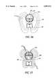
- FIG. 17ashows an alternative embodiment to a rotating element with two magnetic segments.
- FIG. 17bshows an alternative embodiment to a rotating element with one magnetic segment.
- FIG. 18shows a cross-sectional view of a fourth embodiment of a gyricon sheet according to the present invention.
- FIG. 19shows a cross-sectional view of a fifth embodiment of a gyricon sheet according to the present invention.
- FIG. 20shows a cross-sectional view of a sixth embodiment of a gyricon sheet according to the present invention with a rotating element in a first orientation.
- FIG. 21shows a cross-sectional view of a sixth embodiment of a gyricon sheet according to the present invention with a rotating element in a second orientation.
- FIG. 22shows a cross-sectional view of a seventh embodiment of a gyricon sheet according to the present invention.
- FIG. 23shows a cross-sectional view of a eighth embodiment of a gyricon sheet according to the present invention.
- FIG. 24shows a first step in a process used to make a gyricon sheet shown in FIG. 23.
- FIG. 25shows a second step in a process used to make a gyricon sheet shown in FIG. 23.
- FIG. 26shows a cross-sectional view of a ninth embodiment of a gyricon sheet according to the present invention.
- FIG. 27shows a cross-sectional view of a tenth embodiment of a gyricon sheet according to the present invention.
- FIG. 28shows a cross-sectional view of a eleventh embodiment of a gyricon sheet according to the present invention with a rotating element in a first orientation.
- FIG. 29shows a cross-sectional view of a eleventh embodiment of a gyricon sheet according to the present invention with a rotating element in a second orientation.
- FIG. 30shows a cross-sectional view of a twelfth embodiment of a gyricon sheet according to the present invention with a rotating element in a first orientation.
- FIG. 31shows a cross-sectional view of a twelfth embodiment of a gyricon sheet according to the present invention with a rotating element in a second orientation.
- FIG. 32shows a step in a process used to make a gyricon sheet shown in either FIGS. 28 and 29 or FIGS. 31 and 32.
- FIG. 33shows a cross-sectional view of a prior art gyricon.
- FIG. 34shows a cross-sectional view of a thirteenth embodiment of a gyricon sheet according to the present invention.
- FIG. 35shows a cross-sectional view of a fourteenth embodiment of a gyricon sheet according to the present invention.
- FIG. 36shows a cross-sectional view of a magnetic model of a gyricon sheet shown in any of FIGS. 20-24.
- FIG. 37shows a cross-sectional view of a magnetic model of a gyricon sheet shown in any of FIGS. 20-24.
- FIG. 38shows the cross-sectional view shown in FIG. 37 with an additional magnet added.
- FIG. 39shows a first step in an addressing process, according to the present invention, for a gyricon sheet shown in FIGS. 20-24.
- FIG. 40shows a second step in an addressing process, according to the present invention, for a gyricon sheet shown in FIGS. 20-24.
- FIG. 41shows a third step in an addressing process, according to the present invention, for a gyricon sheet shown in FIGS. 20-24.
- FIG. 42shows a fourth step in an addressing process, according to the present invention, for a gyricon sheet shown in FIGS. 20-24.
- FIG. 43shows a first step in an addressing process, according to the present invention, for a gyricon sheet shown in FIGS. 20-24.
- FIG. 44shows a second step in an addressing process, according to the present invention, for a gyricon sheet shown in FIGS. 20-24.
- FIG. 45shows a third step in an addressing process, according to the present invention, for a gyricon sheet shown in FIGS. 20-24.
- FIG. 46shows a fourth step in an addressing process, according to the present invention, for a gyricon sheet shown in FIGS. 20-24.
- FIG. 47shows a first step in an addressing process, according to the present invention, for a gyricon sheet shown in FIGS. 20-24.
- FIG. 48shows a second step in an addressing process, according to the present invention, for a gyricon sheet shown in FIGS. 20-24.
- FIG. 49shows a third step in an addressing process, according to the present invention, for a gyricon sheet shown in FIGS. 20-24.
- FIG. 50shows a fourth step in an addressing process, according to the present invention, for a gyricon sheet shown in FIGS. 20-24.
- FIG. 51shows a cross-section of a gyricon sheet shown in FIGS. 20-24 after it has been addressed according to the process shown in FIGS. 47-50.
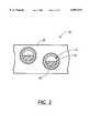
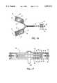
- FIG. 1a prior art Gyricon sheet 10 is shown.
- the gyricon sheetconsists of spherically symmetric rotating elements 12 with anisotropic electrical and optical properties.
- the rotating element 12can be made to rotate and thus exhibit changes in optical properties by the imposition of external electrical fields.
- FIG. 1portrays a gyricon sheet 10 as disclosed in U.S. Pat. No. 4,143,103 by Sheridon, titled “Method Of Making A Twisting Ball Panel Display", and incorporated by reference hereinabove in the form of a bichromal rotating element having segments 14, 16 with different electrical and optical properties.
- This rotating element 12is located in an oil filled cavity 18 in a transparent optical medium 20. When voltages are applied to addressing electrodes (not shown) the rotating element 12 will rotate, presenting either the black segment 14 or the white segment 16 to the viewer.
- the gyricon sheet 10is composed of a transparent optical medium 20, with an oil filled cavity 18 enclosing a rotating element 12. However, due to the manufacturing process a skin 19 is interposed between the oil filled cavity 18 and the transparent optical medium 20 and encloses the oil filled cavity 18.
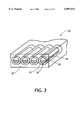
- FIG. 3shows an example of a gyricon sheet 22 which has cylindrically symmetric rotating elements 24 with anisotropic electrical and optical properties. Notice that the cross-section of a spherically or cylindrically symmetric element is the same. The rotating element 24 can also be made to rotate and thus exhibit changes in optical properties by the imposition of external electrical fields.
- FIG. 3portrays a gyricon sheet 22 as disclosed in U.S. patent application Ser. No. 08/716,672 by Sheridon et al. and titled “Twisting Cylinder Display” and herein incorporated by reference in the form of a bichromal cylinder having surfaces 26, 28 with different electrical and optical properties.
- This rotating element 24is located in an oil filled cavity 30 in a transparent optical medium 32. When voltages are applied to addressing electrodes (not shown) the rotating element 24 will rotate, presenting either the black surface 26 or the white surface 28 to the viewer.
- the following devicesall incorporate a "soft magnetic material” in the construction of a gyricon sheet.
- the term “soft magnetic material”is used to describe a magnetic material that is capable of developing a strong magnetic dipole strength while exposed to a strong external magnetic field, but that is not capable of retaining significant remnant magnetism when no longer exposed to the external field.
- hard magnetic materialswhich retain significant magnetism when no external field is present, for example a permanent magnet.
- Soft magnetic materialsinclude paramagnetic materials, ferromagnetic materials, ferromagnetic materials and supermagnetic materials, all of which may be suitable for use in the present application.
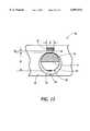
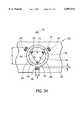
- FIG. 4a cross-section of a portion of a magnetically assisted Gyricon sheet 46 made from a transparent optical medium 44.
- a cross-section of a black and white bichromal spherical or cylindrical rotating element 34is shown in which a black magnetized segment 40 is made from black pigments, some of which are permanently magnetizable. It should be noted that black and white are used here for illustrative purposes only and any colors could be chosen.
- a white unmagnetized segment 38is constructed from the usual materials and is not magnetizable.
- This rotating element 34is contained in an oil filled cavity 36.
- a soft magnetic material pad 42is incorporated near the cavity structure of each rotating element 34 as shown in FIG. 4 and separated from the oil filled cavity by a separation distance D s .
- the soft magnetic material pad 42should preferably have a length l no smaller than 1/4 of the rotating element diameter d.
- the only restriction on the upper limit of the length lis that it must not be so large as to interfere with surrounding rotating elements or their soft magnetic material pads. This will be dictated by the packing density of the gyricon sheet 46.
- the length l of the soft magnetic material pad 42can be as large as the diameter d of the rotating element 34 or even twice as large as the diameter d of the rotating element 34 or more.
- the rotating element 34is also made from materials that develop electrical potentials in contact with the liquid in the oil filled cavity 36 and in the presence of the electrical field, so that the two segments 38, 40 of the rotating element 34 develop different electrical potentials from each other.
- the black magnetized segment 40 of the rotating element 34When the black magnetized segment 40 of the rotating element 34 is adjacent to the soft magnetic material pad 42 embedded next to the oil filled cavity 36, a strong magnetic force tends to hold the rotating element 34 in place. This is because the distance between the magnetized portion of the rotating element and the soft magnetic material pad 42 is short compared to the dimensions of the magnetized portion of the rotating element, thus providing a strong magnetic field. For practical purposes, the separation distance D s between the rotating element 34 and the soft magnetic material pad 42 should be no more than the diameter d of the rotating element 34 multiplied by a factor of three. This magnetic force will cause the rotating element 34 to be attached to the oil filled cavity 36 wall.
- the magnetic forcewill also require a larger electrical field than otherwise to cause the rotating element 34 to start to rotate in the oil filled cavity 36 because the electrical field must first overcome the magnetic force to cause the rotating element 34 to rotate.
- the gyricon sheet 46may be addressed by any of the addressing methods described herein above or known in the art. Once the rotating element 34 has rotated a short distance it will experience a much reduced force from interaction with the soft magnetic material pad 42 and the motion of the rotating element 34 will be dominated by the applied electrical field. Therefore if a rotating element 34 is aligned in its oil filled cavity 36 in an orientation in which the magnetized segment 40 is adjacent to the soft magnetic material pad 42, a strong electrical field will be required to initiate rotation.
- the threshold value of electrical field required to initiate rotationcan be made uniform and sharp. This is because the effects of the magnetic field on the threshold voltage will dominate over other effects on the threshold voltage, for instance that of non-uniformities in size or chemical composition.
- the rotating element 34can be fabricated with a modified rotating disk assembly, as described in U.S. Pat. No. 5,262,098 by Crowley et al. titled “Method And Apparatus For Fabrication Bichromal Balls For A Twisting Ball Display”, and U.S. patent application Ser. No. 08/716,672 by Sheridon et al. titled “Twisting Cylinder Display” and incorporated by reference hereinabove, or other planar stream free jet type devices such as those disclosed in U.S. Pat. No. 5,344,594, titled “Method For Fabrication Of Multicolored Balls For A Twisting Ball Display", by Sheridon and also incorporated by reference hereinabove. Also, a method for making bichromal spheres with a magnetic hemisphere is disclosed in U.S. Pat. No. 4,810,431 by Leidner and titled “Method Of Manufacturing Plastic Particles For A Particle Display.”
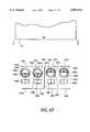
- FIG. 5shows a separator member 70, having two opposed surfaces 72, 74 connected at edge 76, over which two fine planar streams 80, 82 of hardenable material are flowing.
- planar stream 80contains a white pigment
- planar stream 82contains a magnetic pigment similar to that used in the manufacture of magnetic tapes, such as black magnetic pigment Type 031182 by Wright Industries, Brooklyn, New York either alone or in conjunction with other black pigments as are known in the art.
- the planar streams 80,82form an outboard reservoir 84 of liquid which contains equal, side-by side, amounts of each liquid from each planar stream 80, 82.
- a free jet 86 of liquidis formed from the reservoir 84 when the flow rate of the liquids away from the edge 76 is great enough.
- Methods known in the art for creating a free jet 86include a spinning disk assembly and a paddle wheel assembly which are described in U.S. Pat. No. 5,262,098 by Crowley et al. titled “Method And Apparatus For Fabrication Bichromal Balls For A Twisting Ball Display", and a jet assembly, a planar sheet liquid sheet, and a cylindrical liquid sheet described in U.S. Pat. No. 5,344,594, titled “Method For Fabrication Of Multicolored Balls For A Twisting Ball Display", by Sheridon, any of which may be suitably used. If low viscosity hardenable liquids are used, the free jet 86 breaks up into rotating elements 88 at its distal end as shown in FIG. 5.
- While the rotating elements 88are in flight from the free jet 86, they pass through a steady magnetic field 94, which is shown being created by two magnets 90, 92. As the rotating elements 88 pass through the magnetic field the section of the rotating elements 88 containing the magnetic pigment will become magnetized. As the rotating elements 88 are identically oriented with respect to their trajectories, they will be identically magnetized with respect to their geometric poles.
- the steady magnetic fieldmay be created by any number of ways known in the art, for example, a permanent magnet, an electromagnet, an electric field or a direct current flowing through a coil. To properly magnetize the magnetic pigment the magnetic field 94 should be at least 50 gauss.
- the placement of the magnetic field 94 relative to the separator member 70is illustrative only.
- the magnetic field 94could be placed closer to or further away from the separator member 70. For instance, if placed closer, the magnetic field 94 would magnetize the magnetic particles before the free jet 86 breaks up into the rotating elements 88. If placed further away, the magnetic field 94 would magnetize the magnetic particles after the rotating elements 88 have hardened.
- the free jet 86forms filaments which are suitable for making cylindrically symmetric rotating elements 34. As shown in FIG. 5, with respect to spheres 88, if the filaments are passed between a magnetic field 94 while they are being spun, the magnetic pigment will be magnetized and all filaments will be identically magnetized.
- FIG. 6shows an implementation of the technique described above with respect to FIG. 5 using a spinning disk assembly 96.
- the separator member 70is implemented by a spinning disk which rotates around a spindle 98,
- the separator memberhas two surfaces 72, 74 connected at edge 76, over which two fine planar streams 80, 82 of low viscosity hardenable material are flowing.
- planar stream 80contains a white pigment
- planar stream 82contains a magnetic pigment similar to that used in the manufacture of magnetic tapes, such as black magnetic pigment type 031182 by Wright Industries, Brooklyn, N.Y. either alone or in conjunction with other black pigments as are known in the art.
- the planar streams 80, 82form an outboard reservoir 84 of liquid which contains equal, side-by side, amounts of each liquid from each planar stream 80, 82.
- a free jet 86 of liquidis formed from the reservoir 84, in an approximately planar area outward from the reservoir, when the flow rate of the liquids away from the edge 76 is great enough.
- the free jet 86breaks up into rotating elements 88 at its distal end. While the rotating elements 88 are in flight from the free jet 86, they pass through a steady magnetic field 94, which is shown being created by two torous-shaped magnets 90, 92. As the rotating elements 88 pass through the magnetic field the section of the rotating elements 88 containing the magnetic pigment will become magnetized. As the rotating elements 88 are identically oriented with respect to their trajectories, they will be identically magnetized with respect to their geometric poles.
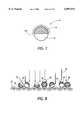
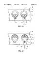
- the gyricon sheet 46 with the soft magnetic material pad 42can be fabricated by first mixing the magnetized rotating element 34 with a soft magnetic material powder such as Black Pigment #V-302 by the Ferro Corp, Brooklyn N.Y.
- the soft magnetic material particles 100would cluster around the magnetized segment 40 as shown in FIG. 7.
- Surplus particles 100are removed from the rotating elements 34 by placing them in a fluidized bed or placing them on a screen 102 where they are washed with controlled air jets 104 as shown in FIG. 8.
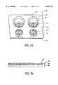
- the rotating elements 34are then mixed with a liquid resin and spread out onto a thin layer on a flat surface to form an uncured sheet 106 a shown in FIG. 9.
- a uniform magnetic field 108is applied to cause the magnetized rotating elements 34 to rotate into common alignment with each other.
- the magnetic pigment 100will also migrate to remain adjacent to the magnetized segment 40.
- the sheetis cured into a tough silicone elastomer, as is known in the art.
- the elastomeris swelled by placing it into an oil bath as is also know in the art.
- the powdered soft magnetic material particles 100have thus been incorporated into the elastomer matrix to form the soft magnetic material pad 42 in the vicinity of the magnetized segment 40 of the rotating element 34 shown in FIG. 4.
- FIG. 4shows a cross-sectional view for either a spherically or cylindrically shaped rotating element 34 the pad will tend to form in a circular shape for a spherically shaped rotating element 34 or in an elongated shape for a cylindrically shaped rotating element.
- the gyricon sheet 46 with the soft magnetic material pad 42can be fabricated as part of an addition to a gyricon sheet which has been made using any method of creating a gyricon sheet including those described hereinabove or any of the references incorporated hereinabove and using magnetizable elements.
- the sheetmay be constructed using either rotating elements 34 that are pre-magnetized, as used above, or containing magnetizable but not yet magnetized rotating elements 34. If the sheet 46 is constructed using rotating elements 34 that have not been magnetized, then once the sheet has been constructed and soaked in oil so that the rotating elements 34 may rotate, a uniform electric field is applied to orient the rotating elements 34 in a common direction, as is known in the art. Once the rotating elements 34 have been oriented in a common direction a strong magnetic field 94, as detailed hereinbefore, is applied to magnetize the rotating elements 34 uniformly as shown in FIG. 10.
- a thin layer 110 of uncured or molten materialsuch as an uncured elastomer, epoxy or a molten polymer, containing powdered soft magnetic material particles 100 is adhered to one side of the gyricon sheet.
- the powdered soft magnetic material particles 100will be attracted towards the magnetic segments 40 of the rotating elements and migrate to form the soft magnetic material pads 42 as shown in FIG. 11.
- the thin layer 110 containing the particles 100is cured or otherwise solidified, locking the soft magnetic material pads 42 in place.
- FIG. 4shows a cross-sectional view for either a spherically or cylindrically shaped rotating element 34 and the pad 42 will tend to form in a circular shape for a spherically shaped rotating element 34 or in an elongated shape for a cylindrically shaped rotating element.
- the gyricon sheet 46 with the soft magnetic material pad 42can be formed by mixing into an uncured elastomer soft magnetic material powder 100 and magnetized rotating elements 34. This is formed into an uncured sheet 106 on a surface, and the curing is delayed to allow the pigment particles 100 to be attracted to the magnetized segments 40 of the rotating elements 34. This pigment particles 100 will be attracted to the magnetized segments 40 because the magnetized segments 40 create a very non-uniform magnetic field in their vicinities. This field provides the mechanical force to move the pigment particles to the surface of the magnetized segments 40 of the rotating elements.
- a uniform magnetic field 108shown in this example being created using two magnets 89, 91 is applied to the sheet, causing the rotating elements 34 and the attached soft magnetic material pigment particles 100, to rotate into common alignment. As is shown in FIG. 12. While this field is continuously applied the elastomer sheet is cured as is known in the art. The sheet can then be swelled, as is also known in the art.
- FIG. 4shows a cross-sectional view for either a spherically or cylindrically shaped rotating element 34 the pad will tend to form in a circular shape for a spherically shaped rotating element 34 or in an elongated shape for a cylindrically shaped rotating element.
- a controlled thresholdis provided by using a rotating element which incorporates a single magnetic segment interacting with a single soft magnetic material pad located adjacent to the oil-filled cavity containing the rotating element.
- thisprovides threshold control for only the rotational transition when the magnetized portion of the rotating element is adjacent to the soft magnetic material pad and the rotating element is being rotated so that this portion is at the opposite side of the cavity. This is good enough for many applications. a For some passive addressing applications however, it is desired to rotate elements into both polarities electronically, without first erasing the whole image. In these applications there is a need for two thresholds, one for each rotation state.
- FIG. 13is shown a cross-section of a portion of a magnetically assisted Gyricon sheet 46.
- a black and white bichromal rotating element 34is shown in which the black magnetized segment 40 is made from black pigments, some of which are permanently magnetizable. It should be noted that black and white are used here for illustrative purposes only and any colors could be chosen.
- the white unmagnetized segment 38is constructed from the usual materials and is not magnetizable.
- This rotating element 34is contained in an oil filled cavity 36. In contrast to FIG. 4, two soft magnetic material pads 42 are incorporated near the cavity structure of each rotating element in an opposed configuration.
- the rotating element 34is also made from materials that develop electrical potentials in contact with the liquid in the oil filled cavity 36 and in the presence of the electrical field, so that the segments 38, 40 of the rotating element 34 develop different electrical potentials from each other.
- the black magnetized segment 40 of the rotating element 34When the black magnetized segment 40 of the rotating element 34 is adjacent to either of the soft magnetic material pads 42 embedded next to the oil filled cavity 36, a strong magnetic force tends to hold the rotating element 34 in place. This is because the distance between the magnetized portion of the rotating element 34 and the soft magnetic material pad 42 is very short compared to the dimensions of the magnetized portion of the rotating element, thus providing a strong magnetic field.
- the separation distance between D s the rotating element 34 and the soft magnetic material pad 42should be no more than the diameter d of the rotating element 34 multiplied by a factor of three.
- the soft magnetic material pad 42should preferably have a length l no smaller than 1/4 of the rotating element diameter d.
- the only restriction on the upper limit of the length lis that it must not be so large as to interfere with surrounding rotational elements or their soft magnetic material pads. This will be dictated by the packing density of the gyricon sheet 46. Depending on the packing density, and the length l of the soft magnetic material pad 42 can be as large as the diameter d of the rotating element 34 or even twice as large as the diameter d of the rotating element 34 or more. This magnetic force will cause the rotating element 34 to be attached to the oil filled cavity 36 wall, and will also require a larger electrical field than otherwise to cause the rotating element 34 to start to rotate in the oil filled cavity 36.
- the rotating element 34Once the rotating element 34 has rotated a short distance it will experience a much reduced force from interaction with the soft magnetic material pad 42 and the motion of the rotating element 34 will be dominated by the applied electrical field. Therefore if a rotating element 34 is aligned in its oil filled cavity 36 in an orientation in which the magnetized segment 40 is adjacent to either of the soft magnetic material pads 42, a strong electrical field will be required to initiate rotation.
- the threshold value of electrical field required to initiate rotationcan be made uniform and sharp. This is because the effects of the magnetic field on the threshold voltage will dominate over other effects on the threshold voltage.
- Using a rotating element 34 with a magnetic segment and two soft magnetic material padsprovides thresholds for both states of rotation.
- Two magnetic soft magnetic material pads 42are used, one for each desired orientation of the rotating element, and therefore, the threshold is controlled for both states in contrast to the embodiment described above and shown in FIG. 4. This enhancement would be useful in providing for the sharp threshold and image storage requirements needed to effectively implement passive addressing.
- This sheetmay be fabricated using any of the methods described above to obtain the initial sheet. However, this results in providing only one soft magnetic material pad 42, and two soft magnetic material pads 42 are desired. Therefore, once an initial sheet is fabricated having one soft magnetic material pad 42 the second pad can be provided using the thin layer technique described above and discussed with respect to FIG. 14.
- an electric fieldcan be applied as known in the art to orient the magnetized rotatable particles 34 in a common direction where the magnetized segment 40 has been rotated away from the soft magnetic material pad 42.
- a thin layer 110 of uncured or molten materialsuch as an uncured elastomer, epoxy or a molten polymer, containing powdered soft magnetic material particles 100 is adhered to the side of the gyricon sheet which does not have soft ferromagnetic materials pads 42 and towards which the magnetized segments 40 of the rotatable elements 34 have been oriented.
- the powdered soft magnetic material particles 100will be attracted towards the magnetic segments 40 of the rotating elements 34 and form the soft magnetic material pads 42 as shown in FIG. 14. At this point the thin layer 110 containing the particles 100 is cured or otherwise solidified, locking the soft magnetic material pads 42 in place.
- FIG. 4shows a cross-sectional view for either a spherically or cylindrically shaped rotating element 34 the pad will tend to form in a circular shape for a spherically shaped rotating element 34 or in an elongated shape for a cylindrically shaped rotating element.
- FIG. 15shows a cross-section of a gyricon sheet 46.
- This sheetis a variant of the sheet 46 shown in FIG. 4 and the same reference numerals will be used for the same elements.
- the sheet 46is made from a transparent optical medium 44 with an oil filled cavity 36 which contains a rotating element 52.
- Rotating element 52is a spherically or cylindrically symmetric bichromal element containing, for example, a black segment 54 and a white segment 56. Additionally, rotating element 52 contains two small polar magnetic segments 58, 60 where polar magnetic segment 58 is located adjacent to the black segment 54 and polar magnetic segment 60 is located adjacent to the white segment 56. Further, if the junction J of the segments 54, 56 is viewed as an equatorial line then the magnetic segments are located at the "poles" of the rotating element 52.
- a single soft magnetic material pad 42is contained within the transparent optical medium 44 adjacent to the oil filled cavity 36, as shown in the FIG. 15.
- the two magnetic segments 58, 60interact with the soft magnetic material pad 42 to provide the rotating element with two rotational positions in which the threshold is controlled by magnetic fields.
- Each magnetic segment 58, 60interacts with the soft magnetic material pad 42 in the same manner as described above with respect to FIG. 4. That is, when one of the magnetic segments 58, 60 of the rotating element 52 is adjacent to the soft magnetic material pad 42 that is embedded next to the oil filled cavity 36, a strong magnetic force tends to hold the rotating element 52 in place. This is because the distance between the magnetic segments 58, 60 of the rotating element 52 and the soft magnetic material pad 42 is very short compared to the dimensions of the magnetized portions of the rotating element.
- the separation distance D s between the rotating element 34 and the soft magnetic material pad 42should be no more than the diameter d of the rotating element 34 multiplied by a factor of three.
- the soft magnetic material pad 42should preferably have a length l no smaller than 1/4 of the rotating element diameter d.
- the only restriction on the upper limit of the length lis that it must not be so large as to interfere with surrounding rotational elements or their soft magnetic material pads. This will be dictated by the packing density of the gyricon sheet 46.
- the length l of the soft magnetic material pad 42can be as large as the diameter d of the rotating element 34 or even twice as large as the diameter d of the rotating element 34 or more.
- This magnetic forcewill cause the rotating element 52 to be latched in place, and will also require a larger electrical field than otherwise to cause the rotating element 52 to start to rotate in the oil filled cavity 62. Once the rotating element 52 has rotated a short distance the polar magnetic segment will experience a much reduced force from the soft magnetic material pad 42 it had been adjacent to and the motion of the rotating element 52 will be dominated by the applied electrical field.
- Using a rotating element 52 with two polar magnetic segments 58, 60 and one soft magnetic material pad 42provides thresholds for both states of rotation.
- Two polar magnetic segments 58, 60are used, one for each desired orientation of the rotating element 52, and therefore, the threshold is controlled for both states, in contrast to the embodiment described above and discussed with respect to in FIG. 4.
- the magnetized portion of the rotating element 52is confined to two small polar magnetic segments 58, 60. While it would be possible to implement this variation using a rotating element which uses the large magnetized segment 40 of the rotating element shown in FIG. 4 combined with a single polar magnetic segment 58, 60 of the type shown in the rotating element shown in FIG. 18, using two small polar magnetic segments 58, 60 as shown in FIG. 18 provides a finer control, more precise control. These enhancements would be useful in providing for the sharp threshold and image storage requirements needed to effectively implement passive addressing.
- This rotating elementcan be fabricated as know in the art with a modified multiple rotating disk assembly, as described in U.S. Pat. No. 5,717,514 by Sheridon titled “Polychromal Segmented Balls For A Twisting Ball Display", and U.S. patent application Ser. No. 08/960,865 by Sheridon et al. titled “Twisting Cylinder Display” and incorporated by reference hereinabove, or other planar stream/free jet type devices such as those disclosed in U.S. Pat. No. 5,344,594, titled “Method For Fabrication Of Multicolored Balls For A Twisting Ball Display", by Sheridon and also incorporated by reference hereinabove.
- the manufacturing devices discussed beloware variations on those discussed with respect to FIGS. 5 and 6 and the same reference numerals will be used to identify the same elements.
- FIG. 16shows two separator members 70, each having two opposed surfaces 72, 74 connected at edge 76, over each of which two fine planar streams 80, 82 of hardenable material are flowing.
- outward planar streams 80contain a magnetic pigment similar to that used in the manufacture of magnetic tapes, such as black magnetic pigment Type 031182 by Wright Industries, Brooklyn, N.Y. either alone or in conjunction with other black pigments as are known in the art
- inward planar streams 82each contain one of the pigments used to provide the segment colorations of the rotating elements 88.
- one of the inward streams 82may contain a white pigment while the other of inward planar streams 82 may contain a black pigment.
- planar streams 80, 82combine to form a free jet 86 of liquid which contains side-by side, amounts of each liquid from each planar stream 80, 82 from each separator member 70.
- the outward planar streams 80may contain a smaller volume of material than the inward planar streams 82.
- the free jet 86 of liquidis formed when the flow rate of the liquids away from the edge 76 is great enough.
- Methods known in the art for creating a free jet 86include a spinning disk assembly as described in U.S. Pat. No. 5,717,514 by Sheridon titled “Polychromal Segmented Balls For A Twisting Ball Display", and a jet assembly, a planar sheet liquid sheet, and a cylindrical liquid sheet described in U.S. Pat. No. 5,344,594, titled “Method For Fabrication Of Multicolored Balls For A Twisting Ball Display", by Sheridon, any of which may be suitably used. If low viscosity hardenable liquids are used the free jet 86 breaks up into rotating elements 88 at its distal end as shown in FIG. 16.
- While the rotating elements 88are in flight from the free jet 86, they pass through a steady magnetic field 94, which is shown being created by two magnets 90, 92. As the rotating elements 88 pass through the magnetic field the section of the rotating elements 88 containing the magnetic pigment will become magnetized, As the rotating elements 88 are identically oriented with respect to their trajectories, they will be identically magnetized with respect to their geometric poles.
- the steady magnetic fieldmay be created by any number of ways known in the art, for example, a permanent magnet, an electric field or a direct current through a coil. To properly magnetize the magnetic pigment the magnetic field 94 should be at least 50 gauss.
- the free jet 86forms filaments which are suitable for making cylindrically symmetric rotating elements 34.
- the filamentsare passed between a magnetic field 94 while they are being spun, the magnetic pigment will be magnetized and all filaments will be identically magnetized.
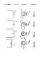
- FIG. 17shows an implementation of the technique described above with respect to FIG. 16 using a multiple spinning disk assembly 96.
- the two separator members 70are each implemented by a spinning disk which rotates around a single spindle 98.
- Each separator memberhas two surfaces 72, 74 connected at edge 76.
- Over each separator member 70two fine planar streams 80, 82 of low viscosity hardenable material are flowing.
- outward planar streams 80contain a magnetic pigment similar to that used in the manufacture of magnetic tapes, such as black magnetic pigment Type 031182 by Wright Industries, Brooklyn, N.Y.
- inward planar streams 82each contain one of the pigments used to provide the segmental colorations of the rotating elements 88.
- one of the inward streams 82may contain a white pigment while the other of inward planar streams 82 may contain a black pigment.
- the planar streams 80,82combine to form a free jet 86 of liquid which contains side-by side, amounts of each liquid from each planar stream 80, 82 from each separator member 76.
- the outward planar streams 80may contain a smaller volume of material than the inward planar streams 82.
- a free jet 86 of liquidis formed from the reservoir 84 when the flow rate of the liquids away from the edge 76 is great enough.
- the free jet 86breaks up into rotating elements 88 at its distal end. While the rotating elements 88 are in flight from the free jet 86, they pass through a steady magnetic field 94, which is shown being created by A two torous-shaped magnets 90, 92. As the rotating elements 88 pass through the magnetic field the section of the rotating elements 88 containing the magnetic pigment will become magnetized, As the rotating elements 88 are identically oriented with respect to their trajectories, they will be identically magnetized with respect to their geometric poles.
- this apparatuscan also be used to create a rotating element 320 with only a single small, polar magnetic segment 326 and two unmagnetized segments 322, 324 as shown in FIG. 17b. Again, only three surfaces would be used. One surface would be used for the black segment, one for the white segment and one for the polar magnetic segment. Such an element could be used interchangeably with the segmentally charged rotating element described above with respect to FIG. 4.
- the sheet 46can be fabricated using the thin layer technique as described above and shown in FIG. 11. Once a plasticized sheet 46 has been obtained with uniformly magnetized rotatable particles 34, an electric field can be applied as known in the art to orient the magnetized rotatable particles 34 in a common direction. Subsequently, a thin layer 110 of uncured or molten material, such as an uncured elastomer, epoxy or a molten polymer, containing powdered soft magnetic material particles 100 is adhered to one side of the gyricon. The powdered soft magnetic material particles 100 will be attracted towards the polar magnetic segment 58 of the rotating elements and form the soft magnetic material pads 42 as described earlier. At this point the thin layer 110 containing the particles 100 is cured or otherwise solidified, locking the soft magnetic material pads 42 in place.
- uncured or molten materialsuch as an uncured elastomer, epoxy or a molten polymer
- FIG. 4shows a cross-sectional view for either a spherically or cylindrically shaped rotating element 34 the pad will tend to form in a circular shape for a spherically shaped rotating element 34 or in an elongated shape for a cylindrically shaped rotating element.
- FIG. 18shows a cross-section of a gyricon sheet 46.
- This sheetis a variant of the sheet 46 shown in FIG. 4 and the same reference numerals will be used for the same elements.
- the sheet 46is made from a transparent optical medium 44 with an oil filled cavity 36 which contains a rotating element 52.
- Rotating element 52is a bichromal element containing, for example, a black segment 54 and a white segment 56. Additionally, rotating element 52 contains two small polar magnetic segments 58, 60 where polar magnetic segment 58 is located adjacent to the black segment 54 and polar magnetic segment 60 is located adjacent to the white segment 56. Further, if the junction 70 of the segments 54, 56 is viewed as an equatorial line then the magnetic segments 58, 60 are located at the "poles" of the rotating element 52.
- Two soft magnetic material pads 42are contained within the transparent optical medium 64 adjacent to the oil filled cavity 36 in an opposed configuration, as shown in the FIG. 18.
- the two magnetic segments 58, 60interact with the two soft magnetic material pads 42 to provide the rotating element with two rotational positions in which the threshold is controlled by magnetic fields.
- Each magnetic segment 58, 60interacts with one of the two soft magnetic material pads 42 in the same manner as described above with respect to FIG. 4. That is, when one of the magnetic segments 58, 60 of the rotating element 52 is adjacent to one of the soft magnetic material pads 42 that is embedded next to the oil filled cavity 36, a strong magnetic force tends to hold the rotating element 52 in place.
- the separation distance D s between the rotating element 52 and the soft magnetic material pad 42should be no more than the diameter d of the rotating element 52 multiplied by a factor of three.
- the soft magnetic material pad 42should preferably have a length l no smaller than 1/4 of the rotating element diameter d. The only restriction on the upper limit of the length l is that it must not be so large as to interfere with surrounding rotational elements or their soft magnetic material pads. This will be dictated by the packing density of the gyricon sheet 46.
- the length l of the soft magnetic material pad 42can be as large as the diameter d of the rotating element 34 or even twice as large as the diameter d of the rotating element 34 or more.
- This magnetic forcewill cause the rotating element 52 to be latched in place, and will also require a larger electrical field than otherwise to cause the rotating element 52 to start to rotate in the oil filled cavity 62. Once the rotating element 52 has rotated a short distance it will experience a much reduced force from the soft magnetic material pad 42 it had been adjacent to and the motion of the rotating element 52 will be dominated by the applied electrical field.
- Using a rotating element 52 with two magnetic segments and two soft magnetic material padsprovides thresholds for both states of rotation. Two magnetic segments and two soft magnetic material pads are used, one for each desired orientation of the rotating element, and therefore, the threshold is controlled for both states, in contrast to the embodiment described above and shown in FIG. 4. Additionally, the magnetized portion of the rotating element is confined to two small polar magnetic segments. While it would be possible to implement this variation using a rotating element which uses the magnetized segment 40 of the rotating element shown in FIG. 4 combined with a single polar magnetic segment 58 of the type shown in the rotating element shown in FIG. 18, using two small polar magnetic segments 58, 60 as shown in FIG. 18 provides a finer more precise control. These enhancements would be useful in providing for the sharp threshold and image storage requirements needed to effectively implement passive addressing.
- FIG. 19shows the gyricon sheet 46 made from transparent optical medium 44 with an oil filled cavity 36 as before.
- the oil filled cavity 36contains a bichromal rotating element 112 with an end segment 114 of a first color and an end segment 116 of a second color different from the first color.
- a magnetic segment 118Interposed between the end segments 114, 116 is a magnetic segment 118.
- the magnetic segment 118is a relatively thin segment, of thickness t, approximately slicing through the center of the rotating element 112.
- a soft magnetic material padin the shape of a soft magnetic material loop or ring 120 surrounding the oil filled cavity 36 again, at approximately the centerline of the oil filled cavity 36.
- the rotating element 112is spherically symmetric than the soft magnetic material ring 120 will be essentially round, as for instance, the rings around Saturn. However, if the rotating element 112 is cylindrically symmetric then the soft magnetic material ring 120 will be an elongated shape.
- the rotating element 112has two equally stable states of orientation, each with a sharp threshold mostly controlled by magnetic fields between the magnetic segment 118 and the soft magnetic material ring 120.
- the separation distance D s between the rotating element 112 and the soft magnetic material ring 120should be no more than the thickness t of the magnetic segment 118 multiplied by a factor of four.
- the soft magnetic material ring 120should preferably have a length l no smaller than 1/4 of the magnetic segment thickness t.
- the length l of the soft magnetic material ring 120can be as large as the thickness t of the magnetic segment 118 or even four as large as the thickness t of the magnetic segment 118 or more.
- the magnetic segment 118interacts with the soft magnetic material ring 120 in the same manner as described above with respect to FIGS. 4 and 18. That is, when the magnetic segment 118 of the rotating element 112 is adjacent to the soft magnetic material ring 120 embedded next to the oil filled cavity 36, a strong magnetic force tends to hold the rotating element 112 in place. This magnetic force will cause the rotating element 112 to be latched in place, and will also require a larger electrical field than otherwise to cause the rotating element 112 to start to rotate in the oil filled cavity 36. Once the rotating element 112 has rotated a short distance it will experience a much reduced force from the soft magnetic material ring 120 and the motion of the rotating element 112 will be dominated by the applied electrical field.
- This configurationallows for latching with either side of the rotating element 112 to be viewable and unobstructed by magnetic latching elements.
- Two separator memberswould be required but only three of the liquid delivery surfaces would be used. One surface would be used for one of the colored end segments, one surface would be used for the other, differently colored end segment and one for the magnetic segment. Again, the magnetic segment in the individual rotating elements can be magnetized by causing the rotating elements to pass through a magnetic field during the fabrication process, as illustrated in FIGS. 16 and 17.
- the soft magnetic material ring 120can also be fabricated by utilizing the same process as the Sheet Fabrication Method 1 described above for the soft magnetic material pads with a single latched state as shown in FIG. 9.
- the magnetized rotating element 112is mixed with a soft magnetic material powder such as Black Pigment #V-302 by the Ferro Corporation, Cleveland, Ohio.
- the powdered particleswould cluster around the magnetized magnetic segment. Again, surplus particles can be removed by the use of a fluidized bed or by placing the balls on a screen and washing them with an air stream.
- the rotating element 112is then mixed with a liquid elastomer and spread out into a thin layer on a flat surface to form a sheet.
- This sheetis next placed between two flat magnets and the magnetic field created by these magnets will cause the magnetized rotating elements to rotate into a common alignment with each other. With this magnetic field present the sheet is cured into a tough silicone elastomer, as is known in the art. After curing, the elastomer is swelled by placing it into an oil bath as is also know in the art. The powdered soft magnetic material particles have thus been incorporated into the elastomer matrix, to form the soft magnetic material ring 120 in the vicinity of the magnetic segment 118 of the rotating element 112.
- the soft magnetic material ring 120can also be fabricated by utilizing the same process as the Sheet Fabrication Method 3 described above for the soft magnetic material pads with a single latched state and shown in FIG. 12.
- the soft magnetic material ring 120can be formed by mixing into an uncured elastomer soft magnetic material powder and magnetized rotating elements 112. This is formed into an uncured sheet on a surface, and the curing is delayed to allow the pigment particles to be attracted to the magnetized segments of the rotating elements 112. The pigment particles will be attracted to the magnetized segments because the magnetized segments create a very non-uniform magnetic field in their vicinities. This field provides the mechanical force to move the pigment particles to the surface of the magnetized segments of the rotating elements.
- FIGS. 1, 2, and 3The rotatable optical Gyricon elements described above in FIGS. 1, 2, and 3 are constrained to stay within cavities that emulate the shapes of the elements. Therefore it is possible to create magnetic traps that ensure the bistability of switching between optical states, and that create modifiable switching thresholds.
- FIG. 20shows a modification of the structure shown in FIG. 4, and therefore the same reference numerals will be used for the same elements.
- FIG. 20shows a gyricon sheet 46 made from a transparent optical medium 44 with an oil filled cavity 36 enclosing a rotating element 34 where one segment 40 is one color and the other segment 38 is a second color.
- the rotating element 34 shown in FIG. 20is the same bichromal rotating element 34 as shown in FIG. 4 and the segment 40 of the rotating element 34 is made from pigments, at least some of which are permanently magnetizable.
- rotating element 320may be used interchangeably with the rotating element 34 shown in this figure and other figures throughout. Adjacent to each oil filled cavity 36 and localized to the dimensions of the rotating element 34 is a pad 134 of permanently magnetized particles 132. This is different from the structure shown in FIG.
- the pad 134 and the magnetized segment 40 of the rotating element 34are magnetized in such a way that when the magnetized segment 40 of the rotating element 34 is rotated to be adjacent to the pad 134 the magnetized segment 40 and the pad 134 are maximally attracted to one another. This can be accomplished by polarizing the magnetic segment 40 and the pad 132 as shown in the diagram where "N" and "S" represent the north and south poles respectively. Thus, when the rotating elements are rotated as shown in FIG. 20 they are held in place by a magnetic field H. In addition, since the magnetic pads 134 are of dimensions comparable to those of the magnetic segment 40, the magnetic field H created by them in the vicinity of the rotating element 34 is strongly non-uniform.
- FIG. 21shows the same gyricon sheet 46 with the rotating element 34 rotated in the opposite configuration as shown in FIG. 20. That is, the rotating element 34 has been rotated such that the magnetic segment 40 is facing away from the pad 134. As can be seen in FIG. 21, the polarization of the magnetic segment 40 and the pad 134 are such that like poles are facing each other and the magnetic segment 40 and the pad 134 will now repel each other.
- the rotating element 34must not undergo slip rotation.
- Experimental observationconfirms that when rotating elements are switched from one optical state to another they rotate as they cross the cavities. Sometimes they even roll along the cavity walls. When they reach the cavity walls adjacent to the addressing electrode they stop all forms of rotary motion. These rotating elements never undergo slip rotation in contact with cavity walls, only rolling rotation.
- the rotating element 34 with its magnetic segment 40 facing upwardis pushed against the cavity wall by the magnetic field. It can roll along the cavity wall, but once it reaches the highest portion of the cavity wall any further rotation will move the magnetic segment 40 closer to the magnetic pad 134, a movement resisted by the repelling force of the magnetic field H. Thus this is a second stable orientation of the rotating element with respect to magnetic field H.
- This sheetcan be fabricated using any of the methods previously described for fabricating a soft magnetic material pad device that is a gyricon with a single latched state and substituting a permanently magnetizable particle, such as Black Magnetic Pigment type 031182 by Wright Industries, Brooklyn, N.Y., for the soft magnetic material particles.
- a permanently magnetizable particlesuch as Black Magnetic Pigment type 031182 by Wright Industries, Brooklyn, N.Y.
- FIG. 22shows an alternative implementation and the same reference numerals will be used to identify the same elements.
- the gyricon sheet 46is made from the transparent optical medium 44 with an oil filled cavity 36 enclosing a rotating element 34 although rotating element 320 shown in FIG. 17b could also be used.
- the magnetic pad 152is constructed from a uniform permanently magnetized rubber sheet which has had etched areas 156 removed to create magnetic hills 154. The etching depth determines the strength of the non-uniform component of the magnetic field created by this magnet.
- the magnetic hills 154have dimensions of the same order as the rotating element 34 and the magnetic pad 152 is aligned with the gyricon sheet 46 such that each magnetic hill 154 is aligned with an oil-filled cavity 36.
- the magnetized segment 40 of the rotating element 34is magnetized in such a way that when the magnetized segment 40 of the rotating element 34 is rotated to be adjacent to the magnetic hill 154 of the magnetic pad 152, the magnetized segment 40 and the magnetic hill 154 are maximally attracted to one another.
- Thiscan be accomplished by polarizing the magnetic segment 40 and the magnetic hill 154 as shown in the diagram where "N" and "S" represent the north and south poles respectively.
- N and Srepresent the north and south poles respectively.
- the rotating elementsare rotated as shown in FIG. 22 they are held in place by a magnetic field H.
- the magnetic hills 154are of dimensions comparable to those of the magnetic segment 150, the magnetic field H created by them is strongly non-uniform.
- the gyricon sheet 46can be made using any of the previously known techniques for creating gyricon sheets and utilizing magnetizable rotating elements, but in particular manufacturing techniques which produce a regular array of rotating elements within a sheet will simplify production and alignment of the magnetic pad 152.
- One such manufacturing techniqueis the "eggcrate” display disclosed in U.S. Pat. No. 5,777,782 by Sheridon, titled “Auxiliary Optics For A Twisting Ball Display” and herein incorporated by reference.
- the "eggcrate” displayproduces a highly, regular geometric pattern of rotating elements which allows for the tight registration and alignment of rotating elements with auxiliary components such as optical components or in this case a patterned magnetic pad.
- the patterned magnetic pad 152can be made by taking a sheet of "rubberized magnet", so called because it consists of a high concentration of magnetic pigment particles dispersed in a rubber binder, and patterning it by several known methods. One method is to coat the surface of the rubberized magnet with a photoresist. The photoresist can then be masked and patterned as is known in the art. If a positive photoresist is used, the gyricon sheet 46 itself can be used as the mask. The rotating elements 34 will block the light rays where a magnetic hill is desired.
- the rubberized magnetcan be etched using acids, such as nitric acid or sulfuric acid, or by using a plasma discharge etching process.
- acidssuch as nitric acid or sulfuric acid
- the depth of the etching process, and thus the strength of the spatially varying portion of the magnetic field,is determined by the strength of the acid and the amount of time spent in the acid.
- a thin aluminum maskcan be created on the sheet of rubberized magnet.
- This sheetwould be overcoated with a photoresist, the latter being exposed using the Gyricon sheet 46 as a photo-mask, as before. If a positive photoresist was used, the exposed areas will be removed. Etching with an acid, such as nitric acid, will leave optically reflective aluminum mirrors over regions corresponding to the rotating element 34 positions.
- the sheet of rubberized magnetcan now be exposed to a strong light source, such as from a laser or a strong incandescent lamp. The strong light source will destroy the magnetic properties of the rubberized magnet, where it is not protected by the aluminum mask (which reflects the light), by heating the sheet above the Curie point. Areas of the rubberized magnet heated above their Curie point will lose their magnetism. Although this does not result in the actual removal of material to form the magnetic hills 154, the effect is the same.
- the patterned magnetic pad 152can be aligned with and adhered to the gyricon sheet using appropriate adhesives or mechanical clamping devices.
- Another approachwould be to coat the surface of the gyricon sheet with a layer of uncured silicone rubber, and apply it to the rubberized magnet. The edges of the thus made composite sheet would next be clamped and the silicone rubber cured. The silicone rubber sheets would adhere poorly, but the clamps at the edges of the sheet would prevent delamination.
- FIG. 23shows an implementation of a gyricon sheet 46 made from a transparent optical medium 44 with an oil filled cavity 36 enclosing a rotating element 34 where one segment 38 is one color and the other segment 40 is a second color.
- the rotating element 34 shown in FIG. 23is the same bichromal rotating element 34 as shown in FIG. 4, however the rotating element 320 shown in FIG. 17b, could also be used.
- the segment 40 of the bichromal rotating elementis made from pigments, at least some of which are permanently magnetizable, such as those used in magnetic recording tapes. Examples of such pigments include Black Magnetic Pigment type 031182 by Wright Industries, Brooklyn, N.Y.
- a second oil filled cavity 172 enclosing a ferro-magnetic element 174is provided. It should be noted that while a round ferro-magnetic element is illustrated, it is not necessary, and it may even be preferable that the ferro-magnetic element 174 not be round. This is due the constraint that the ferro-magnetic element 174 should not itself rotate during the subsequent life of the gyricon sheet 46. This can accomplished in several ways. The first of these is to allow the ferro-magnetic element to, at least partially, stick to the transparent optical medium.
- This affectmight also be accomplished by making the ferro-magnetic element 174 in a shape that is not amenable to rotation, such as one having protrusions or sharp edges which would impede rotation. This affect can also be accomplished by using magnetic balls that release poorly from the silicone elastomer when it is swollen in plasticizing oil.
- a thin permanently magnetic layer 176could be used to hold the ferro-magnetic element 174 in the correct orientation. Such a thin magnetic layer could comprise a thin sheet magnet, a thin layer of magnetic particles or other means.
- ferro-magnetic elements 174that are spherical, is that the same process used to make the rotating elements 34 can be used giving good control of dimensions and insuring that the dimensions of the ferro-magnetic elements 174 are of the same order as the rotating elements 34.
- the ferro-magnetic element 174is aligned within the gyricon sheet 46 such that each ferro-magnetic element 174 is aligned with a rotating element 34.
- the ferro, magnetic element 174could be comprised of magnetic pigments, or for stronger magnetic fields rare earth materials.
- the magnetized segment 40 of the rotating element 34is magnetized in such a way that when the magnetized segment 40 of the rotating element 34 is rotated to be adjacent to the ferro-magnetic element 174 the magnetized segment 40 and the ferro-magnetic element 174 are maximally attracted to one another. This can be accomplished by polarizing the magnetic segment 40 and the ferro-magnetic element 174 as shown in the diagram where "N" and "S" represent the north and south poles respectively.
- the rotating elementswhen they are rotated as shown in FIG. 24 they are held in place by a magnetic field H.
- the ferro-magnetic elements 174are of dimensions comparable to those of the magnetic segment 40, the magnetic field H created by them is strongly non-uniform.
- the gyricon sheet 46 shown in FIG. 23can be constructed by first making a ferro-magnetic particle layer 178 comprising unmagnetized ferro-magnetic elements 34 in uncured elastomer 182 as shown in FIG. 24.
- the ferro-magnetic particle layer 178should be made on a release layer 180 such as Teflon.
- a second layer of uncured elastomer 186 containing rotating elements 34is applied to form a rotating element layer 184 as shown in FIG. 25.
- the thickness of the second layer of elastomer 186should be greater than the diameter of the rotating elements 34, but preferably less than twice the diameter of the rotating elements 34.
- a uniform magnetic field 188is applied in a direction normal to the layer 185, 178 surfaces.
- the uniform magnetic field 188will cause the rotating elements 34 to seek out and align with the ferro-magnetic elements 174 and possibly form strings of rotating elements such as string 190. This is a well known effect and is the basis of the ⁇ magnetic brush ⁇ development systems used in xerography.
- the compound structure of the rotating element layer 184 plus the ferro-magnetic particle layer 178can be cured. During the curing process, both layers 178, 186 will be bonded together.
- any excess rotating elements 34 which have formed strings 190can easily be removed using a knife or by light rubbing because they will be protruding from the cured elastomer 186.
- the compound structure of the cured rotating element layer 184 plus the cured ferro-magnetic particle layer 178can be removed from the release layer 180 and swelled as in known in the art to produce gyricon sheet 46 shown in FIG. 23.
- FIG. 26shows a gyricon sheet 46 which has the magnetic elements of the embodiments shown in both FIG. 4 and FIG. 22, therefore the same reference numerals will be used to donate the same elements.
- FIG. 26is shown a cross-section of a portion of a magnetically assisted Gyricon sheet 46.
- a black and white bichromal spherically or cylindrically symmetric rotating element 34is shown in which the black magnetized segment 40 is made from black pigments, some of which are permanently magnetizable.
- rotating element 320 shown in FIG. 17bcould also be used interchangeably with the rotating element 34.
- black and whiteare used here for illustrative purposes only and any colors could be chosen.
- the white unmagnetized segment 38is constructed from the usual materials and is not magnetizable.
- This rotating elementis contained in an oil filled cavity 36.
- the soft magnetic material pad 42is incorporated near the cavity structure of each rotating element the same as shown in FIG. 4.
- the rotating element 34is also made from materials that develop electrical potentials in contact with the liquid in the oil filled cavity 36 and in the presence of the electrical field, so that the segments 38, 40 of the rotating element 34 develop different electrical potentials from each other.
- a magnetic pad 152has been adhered to the surface of the gyricon sheet which is opposed to the soft magnetic material pad 42.
- the magnetic pad 152is constructed from a uniform permanently magnetized rubber sheet which has had etched areas 156 removed to create magnetic hills 154 as discussed earlier with respect to FIG. 22.
- the devicewould work as a magnetic trap device described hereinabove with additional stability applied from the soft magnetic material pad 42 for the condition when the rotating element 38 is disposed away from and is being repelled by the magnetic pad. It should be noted that this configuration may also use other of the rotating elements discussed hereinabove including the rotating element with a single pole magnetic segment, dual pole magnetic segments, or a rotating element with a single pole magnetic segment and a magnetic segment.
- FIG. 27shows a cross-sectional view of a similar sheet using the same elements as used in FIG. 26, except that the patterned magnetic pad 152 has been replaced with a substantially uniform, thin soft magnetic material layer 210. It should also be noted that rotating element 320 shown in FIG. 17b can be used in this embodiment as well.
- the soft magnetic layer 210functions similarly to the soft magnetic pads 42 discussed herein before.
- the magnetic segment 40 of the rotating element 34induces a non-uniform magnetic attractive force between the magnetic segment 40 and the soft magnetic layer 210.
- This magnetic forcewill cause the rotating element 34 to be attached to the oil filled cavity 36 wall.
- the magnetic forcewill also require a larger electrical field than otherwise to cause the rotating element 34 to start to rotate in the oil filled cavity 36 because the electrical field must first overcome the magnetic force to. cause the rotating element 34 to rotate.
- the gyricon sheet 46may be addressed by any of the addressing methods described herein above or known in the art. Once the rotating element 34 has rotated a short distance it will experience a much reduced force from interaction with the soft magnetic material layer 210 and the motion of the rotating element 34 will be dominated by the applied electrical field.
- a soft magnetic material pad 42is incorporated near the cavity structure of each rotating element as shown in FIGS. 28 and 29. Notice that instead of being on the opposite side of the oil filled cavity 36 from the magnetic pad 152, as shown in FIG. 26, the magnetic pad 42 is place to one side of the oil filled cavity 36. This is to provide two rotational states, of the rotating element 200, which are 90 degrees from one another.
- the magnetic pad 152is constructed from a uniform permanently magnetized rubber sheet which has had etched areas 156 removed to create magnetic hills 154 as discussed earlier.
- the devicewould work as a magnetic trap device described hereinabove with an additional rotational state supplied by the soft magnetic material pad 42.
- the polar magnetic segment 208would interact with either the magnetic pad 152 or the magnetic pad 42 to provide magnetic latching as discussed hereinabove. It should be noted that if the rotating element 200 is rotated from the magnetic pad 152 docked position it may not rotate in a direction that guarantees the polar magnetic segment 208 is adjacent to the soft magnetic material pad 42. For this reason, it is probably advisable not to undergo a complete 90 degree rotation when moving from the first state, shown in FIG. 28 to the second state, shown in FIG. 29. A slightly lesser rotation will ensure that the rotating element will rotate back to the first state in the same direction it took in rotating from the first state. It should be noted that the orientation of the polar magnetic segment 208 with respect to rotating element 200 rotation is guaranteed by the orientation of the rotating element 200 in the electric field.
- the soft magnetic layer 210functions similarly to the soft magnetic pads 42 discussed herein before.
- the magnetic segment 208 of the rotating element 200induces a non-uniform magnetic attractive force between the magnetic segment 208 and the soft magnetic layer 210. This magnetic force will cause the rotating element to be attached to the oil filled cavity wall.
- the magnetic forcewill also require a larger electrical field than otherwise to cause the rotating element 200 to start to rotate in the oil filled cavity 36 because the electrical field must first overcome the magnetic force to cause the rotating element 200 to rotate.
- the gyricon sheet 46may be addressed by any of the addressing methods described herein above or known in the art.
- the rotating element 200Once the rotating element 200 has rotated a short distance it will experience a much reduced force from interaction with the soft magnetic material layer 210 and the motion of the rotating element 200 will be dominated by the applied electrical field.
- the soft magnetic material pad 42 and the soft magnetic material layer 210provide two stable positions for the rotation of the rotating element 200 as the rotating element 200 will be attracted to each of them when it is positioned such that the polar magnetic segment 208 is adjacent to either the soft magnetic material pad 42 or the soft magnet material layer 210.
- This rotating elementcan be fabricated as known in the art with a modified multiple rotating disk assembly, as described in U.S. Pat. No. 5,717,514 by Sheridon titled “Polychromal Segmented Balls For A Twisting Ball Display", and U.S. patent application Ser. No. 08/960,865 by Sheridon et al. titled “Twisting Cylinder Display” and incorporated by reference hereinabove, or other planar stream/free jet type devices such as those disclosed in U.S. Pat. No. 5,344,594, titled “Method For Fabrication Of Multicolored Balls For A Twisting Ball Display", by Sheridon and also incorporated by reference hereinabove.
- the manufacturing process and apparatushas been detailed thoroughly hereinabove with respect to FIGS. 16 and 17.
- the manufacture of rotating element 200requires the same 4 stream process as shown in FIGS. 16 and 17 with one stream to be used for the polar magnetic segment, two streams, one each, to be used for the two transparent end segments and one stream for the colored
- the sheetsmay be fabricated using either Fabrication method 1 or Fabrication Method 3 of the sheet manufacturing techniques discussed hereinabove with respect to Gyricons having a single latched state and shown in FIGS. 7 through 12 . It should be noted however, that when a strong magnetic field is applied to orient the rotating elements in a common direction, as shown hereinabove in FIGS. 7 and 12, that the magnetic field 108 should be oriented in a direction parallel to the plane of the uncured sheet 106 as shown in FIG. 32 when constructing the sheet with the 90 degree latch.
- the soft magnetic material layermay be provided by using the technique discussed herein above with respect to sheet Fabrication method 2 and solidifying the layer before particle migration has taken place. In all other respects, fabrication remains the same.
- FIG. 33shows a cross-sectional view of a gyricon sheet 220 made from a transparent optical medium 222 having an oil filled cavity 224 enclosing a rotating element 226, as shown before.
- this rotating element 226is comprised of a multisided display surface 230 encased in a transparent cylinder 228.
- the multisided display surface 230has three display surfaces 232, 234, 236.
- Each display surfacecan be chosen to be a separate color, black, white or shades of grey to provide a gyricon sheet which can provide greyscale, highlight color or even a full-color RGB display.
- the three display surfaces 232, 234, and 236are selected to be red, blue, and green respectively to provide a full color RGB display.
- the elementis addressed by providing an electric field (not shown) which causes the rotating element 226 to rotate to the orientation desired.
- FIG. 34shows the gyricon sheet 220 shown in FIG. 33 after modifications to enable magnetic latching.
- the rotating elementhas been rotated to a position to allow an Observer O to view the display surface 232, which is colored red.
- the rotating element 226has been modified such that each vertex of the multisided display surface 230 has a magnetic portion resulting in three magnetic vertices 240, 242, 244.
- the magnetic vertexis shown as a small cylinder in the corner of each vertex of the multisided display element, however, this need not be so.
- the entire vertexcould be magnetic, or small magnetic portions of other shapes could be included in the vertice.
- the magnetic verticesare depicted as a small magnetic portion contained within the multisided display surface to eliminate any interference with the viewable color on the display surfaces 232, 234, 236 by the magnetic vertices 240, 242, 244.
- the magnetic vertices 240, 242, 244are made from a magnetic material that has been permanently magnetized such as black magnetic pigment Type 031182 by Wright Industries, Brooklyn, N.Y. as discussed herein before.
- the soft magnetic material pads 246, 248, 250are made from soft magnetic material, a magnetic material that is capable of developing a strong magnetic dipole strength while exposed to a strong external magnetic field, but that is not capable of retaining significant remnant magnetism when the field is removed, as discussed herein before.
- this embodiment of the gyricon sheetworks similar to other embodiments discussed hereinabove. That is, when the magnetized vertices 240, 242, 244 of the rotating element 226 are adjacent to the soft magnetic material pads 246, 248, 250 embedded next to the oil filled cavity 224, a strong magnetic force tends to hold the rotating element 226 in place. This is because the distance between the magnetized portions of the rotating element 226 and the soft magnetic material pads 246, 248, 250 is very short compared to the dimensions of the rotating element 226, thus providing a strong magnetic field.
- the soft magnetic material pads 246, 248, 250are incorporated near the oil filled cavity 224 of each rotating element 226 as shown and separated from the oil filled cavity by a separation distance D s .
- the separation distance D sshould be no more than the diameter d of the rotating element multiplied by a factor of three.
- the soft magnetic material pad 42should preferably have a length l no smaller than 1/4 of the rotating element diameter d.
- the only restriction on the upper limit of the length lis that it must not be so large as to interfere with surrounding rotational elements or their soft magnetic material pads. This will be dictated by the packing density of the gyricon sheet 46.
- the length l of the soft magnetic material pad 42can be as large as the diameter d of the rotating element 34 or even twice as large as the diameter d of the rotating element 34 or more.
- This magnetic forcewill require a larger electrical field than otherwise to cause the rotating element 226 to start to rotate in the oil filled cavity 224. Once the rotating element 226 has rotated a short distance it will experience a much reduced force from interaction with the soft magnetic material pads 246, 248, 250 and the motion of the rotating element 226 will be dominated by the applied electrical field.
- FIG. 35shows a modified version of the gyricon sheet 220 shown in FIG. 34.
- FIG. 35shows a cross-sectional view of a gyricon sheet 220 made from a transparent optical medium 222 having an oil filled cavity 224 enclosing a rotating element 260, as shown before.
- this rotating element 260is comprised of a four sided multisided display surface 264 encased in a transparent cylinder 262.
- the multisided display surface 230has four display surfaces 266, 268, 270, 272.
- Each display surfacecan be chosen to be a separate color, black, white or shades of grey to provide a gyricon sheet which can provide greyscale, highlight color or even a full-color RGB display.
- the four display surfaces 266, 268, 270, 272are selected to be red, blue, and green and black respectively to provide a full color RGB display.
- the elementis addressed by providing an electric field (not shown) which causes the rotating element 260 to rotate to the orientation desired.
- each vertex of the multisided display surface 264has a magnetic portion resulting in four magnetic vertices 274, 276, 278, 280.
- Each magnetic vertexis shown as a small cylinder in the corner of each vertex of the multisided display surface 264, however, this need not be so.
- the entire vertexcould be magnetic, or small magnetic portions of other shapes could be included in the vertex.
- the magnetic verticesare depicted as a small magnetic portion contained within the multisided display surface 264 to eliminate any interference with the viewable color on the display surfaces 266, 268, 270, 272 by the magnetic vertices 274, 276, 278, 280.
- the magnetic vertices 274, 276, 278, 280are made from a magnetic material that has been permanently magnetized such as black magnetic pigment Type 031182 by Wright Industries, Brooklyn, New York as discussed herein before.
- the soft magnetic material pads 282, 284, 286, 288are made from soft magnetic material, a magnetic material that is capable of developing a strong magnetic dipole strength while exposed to a strong external magnetic field, but that is not capable of retaining significant remnant magnetism when the field is removed, as discussed herein before.
- the spacing and dimensions of the soft magnetic material pads 282, 284, 286, 288follow the same parameters as set forth in the discussion hereinbefore with respect to FIG. 34.
- this embodiment of the gyricon sheetworks similar to other embodiments discussed hereinabove. That is, when the magnetized vertices 274, 276, 278, 280 of the rotating element 260 are adjacent to the soft magnetic material pads 282, 284, 286, 288 embedded next to the oil filled cavity 224, a strong magnetic force tends to hold the rotating element 260 in place. This is because the distance between the magnetized portions of the rotating element 260 and the soft magnetic material pads 282, 284, 286, 288 is short compared to the dimensions of the rotating element 260, thus providing a strong magnetic field. This magnetic force will require a larger electrical field than otherwise to cause the rotating element 260 to start to rotate in the oil filled cavity 224. Once the rotating element 260 has rotated a short distance it will experience a much reduced force from interaction with the soft magnetic material pads 282, 284, 286, 288 and the motion of the rotating element 260 will be dominated by the applied electrical field.
- the rotating element shown in FIGS. 34 and 35can be manufactured using known drawing techniques such as those discussed in U.S. Pat. No. 5,894,367 titled "A Twisting Cylinder Display Using Multiple Chromatic Values" and incorporated by reference hereinabove.
- U.S. Pat. No. 5,894,367discloses that a large format display element could be constructed from glass or plastic. After assembly of the large format display element, one end of the large format display element is heated and a pulling device slowly draws filaments from the large format display element.
- four thin cylinders of magnetic materialare added at the vertices.
- the gyricon sheet 220 and the soft magnetic material pads 282, 284, 286, 288can be formed by mixing into an uncured elastomer soft magnetic material powder and magnetized rotating elements as discussed herein above with respect to FIG. 10. This is formed into an uncured sheet on a surface, and the curing is delayed to allow the pigment particles to be attracted to the magnetized vertices of the rotating elements. The pigment particles will be attracted to the magnetized vertices because the magnetized vertices create a very non-uniform magnetic field in their vicinities. This field provides the mechanical force to move the pigment particles to the surface of the magnetized vertices of the rotating elements.
- a uniform magnetic fieldis applied to the sheet, causing the rotating elements and the attached soft magnetic material pigment particles, to rotate into common alignment. as is discussed hereinabove with respect to FIG. 12. While this field is continuously applied the elastomer sheet is cured as is known in the art. The sheet can then be swelled, as is also known in the art.
- FIG. 34shows a cross-sectional view for a cylindrically shaped rotating element and the pad will tend to form in an elongated shape for a cylindrically shaped rotating element.
- the second of theseis to apply a small, localized magnetic field of the opposite polarity to negate the magnetic field holding a rotating element in place.
- This small, localized magnetic fieldwill "unlock" a specific rotating element, or a set of rotating elements, and allow rotation if an electric field of the correct polarity s concurrently applied. While this method has the advantage that smaller strength fields need to be generated it comes at the cost of added complexity in the design of the addressing device.
- the disclosure up to this pointhas focussed on using local magnetic fields to provide greater stability of rotating elements in a gyricon sheet because the rotating elements can be latched into a desired position by using the local magnetic fields.
- the local magnetic fieldsprovide stability against inadvertent rotation of elements that may occur due to stray electrical fields when a gyricon sheet is, for instance, handled in order to address the rotating elements and switch them from one position to another an electric field is applied which is strong enough to overcome the local magnetic field and cause the rotating elements to rotate to a new desired state.
- the local magnetic fieldsnecessarily increase the strength of the electric field needed to cause rotation of the elements.
- the most stable stored imageswill necessarily have the strongest local magnetic fields and require the strongest applied electrical fields to cause rotation of the rotating elements to effect an image change.
- An addressing meansthat does not require the stronger electric fields needed to overcome the strong local magnetic fields can be made by using an external magnetic field which temporarily ⁇ unlocks ⁇ the rotating element in conjunction with a reduced electrical addressing field.
- the external magnetic fieldwill counteract the local magnetic field experienced by the rotating element and effectively lowering the magnetic field experienced by the rotating element.
- the external magnetic fieldthereby permits lower electrical fields to be used for addressing the rotating elements.
- FIGS. 36 and 37show a rotating element 300 trapped in an oil filled cavity 302.
- the rotating element 300has two segments, a magnetic segment 306 and a nonmagnetic segment 304. Additionally, a magnet 308 having dimensions comparable to the rotating element 300 is disposed near the oil filled cavity 302.
- FIGS. 36 and 37are consistent with the description of magnetic trapping devices discussed hereinabove with respect to FIGS. 20-23 and could represent any of the configurations discussed with respect to FIGS. 20-23.
- Additionally shown in FIGS. 36 and 37are dominant magnetic field lines 310 that exist between the rotating element 300 and the magnet 308.
- the rotating element 300is trapped in the position where the magnetic segment 306 is proximate to the magnet 308. This is the position where the magnetic segment 306 and the magnet 308 are oriented so they attract each other.
- the field lines 310are seen to connect between the two magnets, indicating their attraction for each other.
- FIG. 37the rotating element 300 is trapped in the position where the magnetic segment 306 is repulsed by the magnetic 308.
- the dominant magnetic field lines 310 from the magnetic segment 306 and the dominant magnetic field lines of the magnet 308tend to repel each other.
- FIG. 38shows the constructions of FIGS. 36 and 37 where an external magnetic field has been added in the form of a uniform and relatively large magnet 312.
- largeit is meant that the size of the magnet 312 is much larger than the diameter of the rotating elements 300 by a factor of at least 10.
- Two sets of rotating elements 300are depicted. The first set depicts the rotating elements 300 where the magnetic segment 306 is attracted to the magnet 308, as shown in FIG. 36.
- the second setdepicts the rotating elements 300 where the magnetic segment 306 is repulsed by the magnetic 308 as depicted in FIG. 37 .
- the dominant magnetic field lines 310are redrawn to show the influence of the large, relatively uniform magnet 312.
- both the rotating element 300 and the magnetic pad 308are made partially from magnetic material that has a high permeability, many of the magnetic field lines associated with the large, uniform magnet 312 will bend to pass through and around these lesser magnets, as shown in FIG. 38.
- This effectcauses the magnetic field associated with the magnet 312 to be non-uniform in the vicinity of both the rotating elements 300 and their associated magnets 308, creating mechanical forces that will be comparable to and oppositely acting to the forces associated with the magnetic fields 310 that exist between the rotating element 300 and the magnet 308 as shown in FIGS. 36 and 37. Effectively, this external magnetic field is nullifying the effects of the magnetic field associated with the magnet 308.
- the magnet 312is some distance away from rotating element 300 and unable to supply a sufficient magnetic field to affect the rotating element 300.
- the rotating element 300is in the condition in which it is attracted to the magnet 308.
- the magnet 312is approaching the rotating element from the side opposite to the magnet 308.
- FIG. 40shows the magnet 312 being moved closer to the rotating element 300.
- the gradient of its magnetic field in the vicinity of the rotating element 300increases to the point where it provides more attraction to the rotating element 300 than the magnet 308.
- the rotating element 300is lifted from the cavity wall and suspended in the oil filled cavity 302.
- FIG. 41illustrates that when an external electrical field is applied across the rotating element 300 by using a charge differential 314 of the required polarity while the rotating element 300 is suspended in the oil filled cavity 302, the electric field will cause the rotating element 300 to rotate.
- the rotating element 300will also move toward the upper cavity wall of the oil filled cavity 302. This can also happen if the magnet 312 is strong enough to lessen the effect of the magnet 308, but not suspend rotating element 300 within the cavity. In that case, the rotating element 300 will still be in contact with the wall of the oil filled cavity 302, as illustrated in FIG. 39, but will rotate and move towards the upper cavity wall of the oil filled cavity 302 when the electric field is applied.
- FIG. 42shows the removal of magnet 312. As the magnet 312 is pulled away from the rotating element 300, the rotating element 300 will come under the magnetic dominance of the magnet 308 once again, locking it into its new state. The rotating element 300 is now in the orientation where it is repelled by the magnet 308.
- the rotating element 300would not have rotated and upon removal of the magnet 312 the rotating element 300 would simply have returned to its initial condition, as shown in FIG. 39.
- the magnet 312is again depicted some distance away from rotating element 300 and unable to supply a sufficient magnetic field to affect the rotating element 300.
- the rotating element 300is in the orientation in which it is repelled from the magnet 308.
- the magnet 312is approaching the rotating element from the side opposite to the magnet 308.
- FIG. 44depicts the magnet 312 moving closer to the rotating element 300.
- the increasing magnetic field from the magnet 312will eventually cause the rotating element 300 to be repulsed from the upper wall of the oil filled cavity 302 and be suspended in the oil filled cavity 302.
- the force of the magnetic field from the magnet 312also causes the rotating element 300 to begin to rotate.
- FIG. 45shows further movement of the rotating element 300 in the oil filled cavity 302 when the magnet 312 is kept in proximity to the rotating element 300. The force of the magnetic field from the magnet 312 continues to cause the rotating element 300 to rotate.
- FIG. 46shows the result of the rotation.
- the rotating element 300ends up in the stable condition where it is attracted to the magnet 308.
- the rotating element 312will remain locked in place under the influence of the magnetic field from the magnet 308.
- FIGS. 47-51apply the concepts shown in FIGS. 39-46 to show how addressing with a magnetic unlocking device in conjunction with an electrical field work on a gyricon sheet. Because the model and elements used in FIGS. 39-46 is identical to the model used in FIGS. 39-46 the same reference numerals will be used for the same elements, however the letter "a”, “b", “c", or “d” will be appended to the reference numerals to denote a particular rotating element and all the elements associated with that particular rotating element for clarity.
- FIG. 47shows four rotating elements 300a, 300b, 300c, 300d.
- Rotating elements 300a and 300bare oriented in the state where they are attracted to their magnets 308a and 308b respectively.
- Rotating elements 300c and 300dare oriented in the state where they are repelled by their magnets 308c and 308d, respectively.
- a pair of electrodes 316a, 316b, 316c, 316dare associated with each rotating element 300a, 300b, 300c, 300d to represent the application of an electric field across the rotating elements 300a, 300b, 300c, 300d.
- An electric fieldexists when a pair of electrodes 316b has a charge differential 314b placed across it.
- While an electric fieldmay be applied across a pair of electrodes 316b using a charge differential 314b, other methods are also known and may be used such as image wise charge placement on the surface of a sheet.
- the magnet 312is moving closer to the rotating elements 300a, 300b, 300c, 300d but is sufficiently distant from the rotating elements 300a, 300b, 300c, 300d that the magnetic fields from the magnet 312 have no impact on the rotating elements 300a, 300b, 300c, 300d.
- the charge differential 314b on the electrodes 316b and its associated electric fieldis also too small to cause rotation of the rotating element 300b.
- the magnet 312has moved sufficiently close to the rotating elements 300a, 300b, 300c, 300d that its associated magnetic field provides the dominant effect on the rotating elements 300a, 300b, 300c, 300d.
- Rotating elements 300a, and 300bare attracted to the magnet 312 and are suspended in their oil filled cavities 302a, 302b.
- Rotating elements 300c and 300dare repelled from the magnet 312 and are also suspended in their oil filled cavities 302c and 302d
- the magnetic field associated with the magnet 312has started to induce rotation in rotating elements 300c and 300d.
- the charge differential 314b across electrodes 316b and the associated electric fieldis still ineffectual in inducing rotation in rotating element 300b because the magnetic field from magnet 312 is the dominant force.
- FIG. 49shows the return of a steady state condition after the rotation of rotating elements 300c and 300d showing that all the rotating elements 300a, 300b, 300c, and 300d are in the same orientation.
- the magnetic field from magnet 312is still the dominating force.
- a charge differential 314dhas been placed across electrodes 316d to apply and electric field across rotating element 300d. If it is desired that any element be in the opposite state then an electric field must be placed across that element before the magnet 312 is removed to cause rotation of that rotating element. It should be noted that the electric field could have been placed earlier in the process with no harmful effects as has been illustrated with element 300b.
- FIG. 50shows the magnet 312 being moved away from the rotating elements 300a, 300b, 300c, and 300d.
- the effects of its magnetic field on the rotating elements 300a, 300b, 300c, 300dwill decrease.
- the magnet 312 and the magnets 308a, 308b, 308c, 308dwill exert equal and nearly opposite forces on the ball. Under these conditions the electric field exerted by the charge differential 314b, 314d on the electrodes 316b, 316d will cause the associated rotating elements 300b, 300d to rotate.
- FIG. 51shows the stable state of the rotating elements 300a, 300b, 300c, and 300d after the magnet 312 has been completely withdrawn.
- the above sequenceillustrates a magnet 312 of a "north" polarity approaching the rotating elements from one side only. It should be noted that the same sequence can be implemented using a magnet of the opposite polarity so long as it also approaches the rotating elements from the opposite side.
- any of the methods for providing and electric field and addressing a gyricon sheetmay be combined with either a sheet magnet or a scanning magnet of sufficient strength.
- a scanning addressing systemcan be made by combining previously known scanning addressing systems, such as that discussed in U.S. Pat. No. 5,389,945, by Sheridon titled "Writing System Including Paper-Like Digitally Addressed Media and Addressing Device Therefor" and incorporated by reference hereinabove, with a magnet to be scanned as well.
- the magnetic fieldcan be created by using a permanent magnet, or an electromagnet energized by a current flowing through a coil or any other method form creating a magnetic field.
Landscapes
- Physics & Mathematics (AREA)
- General Physics & Mathematics (AREA)
- Engineering & Computer Science (AREA)
- Theoretical Computer Science (AREA)
- Health & Medical Sciences (AREA)
- Life Sciences & Earth Sciences (AREA)
- Molecular Biology (AREA)
- Optics & Photonics (AREA)
- Electrochromic Elements, Electrophoresis, Or Variable Reflection Or Absorption Elements (AREA)
Abstract
Description
Claims (21)
Priority Applications (4)
| Application Number | Priority Date | Filing Date | Title |
|---|---|---|---|
| US09/199,646US6097531A (en) | 1998-11-25 | 1998-11-25 | Method of making uniformly magnetized elements for a gyricon display |
| CA 2289382CA2289382C (en) | 1998-11-25 | 1999-11-12 | Gyricon displays utilizing magnetic addressing and latching mechanisms |
| JP32565799AJP4519966B2 (en) | 1998-11-25 | 1999-11-16 | Material used for rotating element sheet, rotating element used for rotating element sheet, rotating element creation method, rotating element manufacturing apparatus used for rotating element display, and rotating element sheet material manufacturing method |
| EP99123198AEP1005008A3 (en) | 1998-11-25 | 1999-11-25 | Gyricon displays utilizing magnetic addressing and latching mechanisms |
Applications Claiming Priority (1)
| Application Number | Priority Date | Filing Date | Title |
|---|---|---|---|
| US09/199,646US6097531A (en) | 1998-11-25 | 1998-11-25 | Method of making uniformly magnetized elements for a gyricon display |
Publications (1)
| Publication Number | Publication Date |
|---|---|
| US6097531Atrue US6097531A (en) | 2000-08-01 |
Family
ID=22738434
Family Applications (1)
| Application Number | Title | Priority Date | Filing Date |
|---|---|---|---|
| US09/199,646Expired - Fee RelatedUS6097531A (en) | 1998-11-25 | 1998-11-25 | Method of making uniformly magnetized elements for a gyricon display |
Country Status (1)
| Country | Link |
|---|---|
| US (1) | US6097531A (en) |
Cited By (278)
| Publication number | Priority date | Publication date | Assignee | Title |
|---|---|---|---|---|
| US6211998B1 (en)* | 1998-11-25 | 2001-04-03 | Xerox Corporation | Magnetic unlatching and addressing of a gyricon display |
| US6262707B1 (en)* | 1998-11-25 | 2001-07-17 | Xerox Corporation | Gyricon displays utilizing magnetic addressing and latching mechanism |
| US20020021270A1 (en)* | 2000-08-17 | 2002-02-21 | Albert Jonathan D. | Bistable electro-optic desplay, and method for addressing same |
| US6377387B1 (en)* | 1999-04-06 | 2002-04-23 | E Ink Corporation | Methods for producing droplets for use in capsule-based electrophoretic displays |
| US6396621B1 (en) | 2000-12-28 | 2002-05-28 | Xerox Corporation | Gyricon display containing chemical absorbents |
| US20020084877A1 (en)* | 2000-12-28 | 2002-07-04 | Dennis Martell | Bi-chromal ball production apparatus and method |
| US6441946B1 (en) | 2000-11-28 | 2002-08-27 | Xerox Corporation | Swollen gyricon displays and method of making same |
| US6440252B1 (en) | 1999-12-17 | 2002-08-27 | Xerox Corporation | Method for rotatable element assembly |
| US6445490B1 (en) | 2000-11-28 | 2002-09-03 | Xerox Corporation | Encapsulated gyricon spheres |
| US20020130832A1 (en)* | 2001-03-13 | 2002-09-19 | Baucom Allan Scott | Apparatus for displaying drawings |
| US20020171910A1 (en)* | 2001-05-15 | 2002-11-21 | Pullen Anthony Edward | Electrophoretic displays containing magnetic particles |
| US6498674B1 (en) | 2000-04-14 | 2002-12-24 | Xerox Corporation | Rotating element sheet material with generalized containment structure |
| US6504525B1 (en) | 2000-05-03 | 2003-01-07 | Xerox Corporation | Rotating element sheet material with microstructured substrate and method of use |
| US20030011560A1 (en)* | 1998-08-27 | 2003-01-16 | E Ink Corporation | Electrophoretic display comprising optical biasing element |
| US20030053189A1 (en)* | 2001-09-14 | 2003-03-20 | E Ink Corporation | Methods for addressing electro-optic materials |
| US6545671B1 (en) | 2000-03-02 | 2003-04-08 | Xerox Corporation | Rotating element sheet material with reversible highlighting |
| US6549327B2 (en) | 2001-05-24 | 2003-04-15 | Xerox Corporation | Photochromic gyricon display |
| US20030137521A1 (en)* | 1999-04-30 | 2003-07-24 | E Ink Corporation | Methods for driving bistable electro-optic displays, and apparatus for use therein |
| US20030180494A1 (en)* | 2002-03-25 | 2003-09-25 | Lu Y. Martin | Continuous combined pigmented wax compounding and bichromal sphere fabrication process |
| US20030214695A1 (en)* | 2002-03-18 | 2003-11-20 | E Ink Corporation | Electro-optic displays, and methods for driving same |
| US20030222315A1 (en)* | 2002-04-24 | 2003-12-04 | E Ink Corporation | Backplanes for display applications, and components for use therein |
| US6663802B2 (en) | 2001-07-30 | 2003-12-16 | Xerox Corporation | Processes for making bichromal particles for gyricon displays |
| WO2003107315A2 (en) | 2002-06-13 | 2003-12-24 | E Ink Corporation | Methods for driving electro-optic displays |
| US20040009309A1 (en)* | 2002-07-15 | 2004-01-15 | Flex Products, Inc., A Jds Uniphase Company | Magnetic planarization of pigment flakes |
| US20040014265A1 (en)* | 2002-04-24 | 2004-01-22 | E Ink Corporation | Processes for forming backplanes for electro-optic displays |
| US20040012839A1 (en)* | 2002-05-23 | 2004-01-22 | E Ink Corporation | Capsules, materials for use therein and electrophoretic media and displays containing such capsules |
| US6690350B2 (en) | 2001-01-11 | 2004-02-10 | Xerox Corporation | Rotating element sheet material with dual vector field addressing |
| US20040027327A1 (en)* | 2002-06-10 | 2004-02-12 | E Ink Corporation | Components and methods for use in electro-optic displays |
| US6704133B2 (en) | 1998-03-18 | 2004-03-09 | E-Ink Corporation | Electro-optic display overlays and systems for addressing such displays |
| US20040105036A1 (en)* | 2002-08-06 | 2004-06-03 | E Ink Corporation | Protection of electro-optic displays against thermal effects |
| US20040112750A1 (en)* | 2002-09-03 | 2004-06-17 | E Ink Corporation | Electrophoretic medium with gaseous suspending fluid |
| US20040136048A1 (en)* | 1995-07-20 | 2004-07-15 | E Ink Corporation | Dielectrophoretic displays |
| US20040155857A1 (en)* | 2002-09-03 | 2004-08-12 | E Ink Corporation | Electro-optic displays |
| US20040196215A1 (en)* | 2002-12-16 | 2004-10-07 | E Ink Corporation | Backplanes for electro-optic displays |
| US20040202862A1 (en)* | 2003-04-14 | 2004-10-14 | Kazmaier Peter M. | Preparation of micromultichromal spheres |
| US20040226820A1 (en)* | 2003-03-25 | 2004-11-18 | E Ink Corporation | Processes for the production of electrophoretic displays |
| US6822781B1 (en) | 2000-10-24 | 2004-11-23 | Cabot Corporation | Gyricon displays containing modified particles |
| US20040233509A1 (en)* | 2002-12-23 | 2004-11-25 | E Ink Corporation | Flexible electro-optic displays |
| US20040257635A1 (en)* | 2003-01-31 | 2004-12-23 | E Ink Corporation | Construction of electrophoretic displays |
| US20050007653A1 (en)* | 2003-03-27 | 2005-01-13 | E Ink Corporation | Electro-optic assemblies, and materials for use therein |
| US20050012980A1 (en)* | 2003-05-02 | 2005-01-20 | E Ink Corporation | Electrophoretic displays with controlled amounts of pigment |
| US6847347B1 (en) | 2000-08-17 | 2005-01-25 | Xerox Corporation | Electromagnetophoretic display system and method |
| US6864875B2 (en) | 1998-04-10 | 2005-03-08 | E Ink Corporation | Full color reflective display with multichromatic sub-pixels |
| US20050105162A1 (en)* | 2001-03-19 | 2005-05-19 | Paolini Richard J.Jr. | Electrophoretic medium and process for the production thereof |
| US6897848B2 (en) | 2001-01-11 | 2005-05-24 | Xerox Corporation | Rotating element sheet material and stylus with gradient field addressing |
| WO2005054933A2 (en) | 2003-11-26 | 2005-06-16 | E Ink Corporation | Electro-optic displays with reduced remnant voltage |
| US6970154B2 (en) | 2001-01-11 | 2005-11-29 | Jpmorgan Chase Bank | Fringe-field filter for addressable displays |
| US20060007526A1 (en)* | 2004-07-12 | 2006-01-12 | Carla Cannas | Sol-gel nanocoated particles for magnetic displays |
| US7002728B2 (en) | 1997-08-28 | 2006-02-21 | E Ink Corporation | Electrophoretic particles, and processes for the production thereof |
| US7034783B2 (en) | 2003-08-19 | 2006-04-25 | E Ink Corporation | Method for controlling electro-optic display |
| US7067190B1 (en) | 2005-03-29 | 2006-06-27 | Xerox Corporation | Capsules utilizing a lubricant |
| US7075703B2 (en) | 2004-01-16 | 2006-07-11 | E Ink Corporation | Process for sealing electro-optic displays |
| US7110164B2 (en) | 2002-06-10 | 2006-09-19 | E Ink Corporation | Electro-optic displays, and processes for the production thereof |
| US7110163B2 (en) | 2001-07-09 | 2006-09-19 | E Ink Corporation | Electro-optic display and lamination adhesive for use therein |
| US7116466B2 (en) | 2004-07-27 | 2006-10-03 | E Ink Corporation | Electro-optic displays |
| US7119759B2 (en) | 1999-05-03 | 2006-10-10 | E Ink Corporation | Machine-readable displays |
| US7119772B2 (en) | 1999-04-30 | 2006-10-10 | E Ink Corporation | Methods for driving bistable electro-optic displays, and apparatus for use therein |
| US7167155B1 (en) | 1995-07-20 | 2007-01-23 | E Ink Corporation | Color electrophoretic displays |
| US7173752B2 (en) | 2003-11-05 | 2007-02-06 | E Ink Corporation | Electro-optic displays, and materials for use therein |
| US7176880B2 (en) | 1999-07-21 | 2007-02-13 | E Ink Corporation | Use of a storage capacitor to enhance the performance of an active matrix driven electronic display |
| US7190008B2 (en) | 2002-04-24 | 2007-03-13 | E Ink Corporation | Electro-optic displays, and components for use therein |
| US7193625B2 (en) | 1999-04-30 | 2007-03-20 | E Ink Corporation | Methods for driving electro-optic displays, and apparatus for use therein |
| US7206119B2 (en) | 2003-12-31 | 2007-04-17 | E Ink Corporation | Electro-optic displays, and method for driving same |
| US7230750B2 (en) | 2001-05-15 | 2007-06-12 | E Ink Corporation | Electrophoretic media and processes for the production thereof |
| US7230751B2 (en) | 2005-01-26 | 2007-06-12 | E Ink Corporation | Electrophoretic displays using gaseous fluids |
| US7247379B2 (en) | 1997-08-28 | 2007-07-24 | E Ink Corporation | Electrophoretic particles, and processes for the production thereof |
| WO2007104003A2 (en) | 2006-03-08 | 2007-09-13 | E Ink Corporation | Methods for production of electro-optic displays |
| US7312916B2 (en) | 2002-08-07 | 2007-12-25 | E Ink Corporation | Electrophoretic media containing specularly reflective particles |
| US7327511B2 (en) | 2004-03-23 | 2008-02-05 | E Ink Corporation | Light modulators |
| US7365394B2 (en) | 2000-04-18 | 2008-04-29 | E Ink Corporation | Process for fabricating thin film transistors |
| US20080117495A1 (en)* | 1995-07-20 | 2008-05-22 | E Ink Corporation | Dielectrophoretic displays |
| US7382363B2 (en) | 2001-07-27 | 2008-06-03 | E Ink Corporation | Microencapsulated electrophoretic display with integrated driver |
| US7388572B2 (en) | 2004-02-27 | 2008-06-17 | E Ink Corporation | Backplanes for electro-optic displays |
| US20080178867A1 (en)* | 2007-01-30 | 2008-07-31 | Xtreme Energetics Inc | Solid-state sun tracker |
| US7411719B2 (en) | 1995-07-20 | 2008-08-12 | E Ink Corporation | Electrophoretic medium and process for the production thereof |
| US7411720B2 (en) | 2001-05-15 | 2008-08-12 | E Ink Corporation | Electrophoretic particles and processes for the production thereof |
| US7420549B2 (en) | 2003-10-08 | 2008-09-02 | E Ink Corporation | Electro-wetting displays |
| US7453445B2 (en) | 2004-08-13 | 2008-11-18 | E Ink Corproation | Methods for driving electro-optic displays |
| US7477444B2 (en) | 2006-09-22 | 2009-01-13 | E Ink Corporation & Air Products And Chemical, Inc. | Electro-optic display and materials for use therein |
| US7492339B2 (en) | 2004-03-26 | 2009-02-17 | E Ink Corporation | Methods for driving bistable electro-optic displays |
| US7492497B2 (en) | 2006-08-02 | 2009-02-17 | E Ink Corporation | Multi-layer light modulator |
| US7528822B2 (en) | 2001-11-20 | 2009-05-05 | E Ink Corporation | Methods for driving electro-optic displays |
| US7535624B2 (en) | 2001-07-09 | 2009-05-19 | E Ink Corporation | Electro-optic display and materials for use therein |
| US7551346B2 (en) | 2003-11-05 | 2009-06-23 | E Ink Corporation | Electro-optic displays, and materials for use therein |
| US7554712B2 (en) | 2005-06-23 | 2009-06-30 | E Ink Corporation | Edge seals for, and processes for assembly of, electro-optic displays |
| US7583427B2 (en) | 2002-06-10 | 2009-09-01 | E Ink Corporation | Components and methods for use in electro-optic displays |
| US7602374B2 (en) | 2003-09-19 | 2009-10-13 | E Ink Corporation | Methods for reducing edge effects in electro-optic displays |
| US20090256868A1 (en)* | 2008-04-11 | 2009-10-15 | Yun Shon Low | Time-Overlapping Partial-Panel Updating Of A Bistable Electro-Optic Display |
| US7636191B2 (en) | 2003-07-24 | 2009-12-22 | E Ink Corporation | Electro-optic display |
| US7649674B2 (en) | 2002-06-10 | 2010-01-19 | E Ink Corporation | Electro-optic display with edge seal |
| US7649666B2 (en) | 2006-12-07 | 2010-01-19 | E Ink Corporation | Components and methods for use in electro-optic displays |
| US7667886B2 (en) | 2007-01-22 | 2010-02-23 | E Ink Corporation | Multi-layer sheet for use in electro-optic displays |
| US7672040B2 (en) | 2003-11-05 | 2010-03-02 | E Ink Corporation | Electro-optic displays, and materials for use therein |
| US7679814B2 (en) | 2001-04-02 | 2010-03-16 | E Ink Corporation | Materials for use in electrophoretic displays |
| US7688497B2 (en) | 2007-01-22 | 2010-03-30 | E Ink Corporation | Multi-layer sheet for use in electro-optic displays |
| US7826129B2 (en) | 2007-03-06 | 2010-11-02 | E Ink Corporation | Materials for use in electrophoretic displays |
| US7839564B2 (en) | 2002-09-03 | 2010-11-23 | E Ink Corporation | Components and methods for use in electro-optic displays |
| US7843624B2 (en) | 2006-03-08 | 2010-11-30 | E Ink Corporation | Electro-optic displays, and materials and methods for production thereof |
| US7843621B2 (en) | 2002-06-10 | 2010-11-30 | E Ink Corporation | Components and testing methods for use in the production of electro-optic displays |
| US7848006B2 (en) | 1995-07-20 | 2010-12-07 | E Ink Corporation | Electrophoretic displays with controlled amounts of pigment |
| US7893435B2 (en) | 2000-04-18 | 2011-02-22 | E Ink Corporation | Flexible electronic circuits and displays including a backplane comprising a patterned metal foil having a plurality of apertures extending therethrough |
| US7903319B2 (en) | 2006-07-11 | 2011-03-08 | E Ink Corporation | Electrophoretic medium and display with improved image stability |
| US7910175B2 (en) | 2003-03-25 | 2011-03-22 | E Ink Corporation | Processes for the production of electrophoretic displays |
| US7952557B2 (en) | 2001-11-20 | 2011-05-31 | E Ink Corporation | Methods and apparatus for driving electro-optic displays |
| US7952790B2 (en) | 2006-03-22 | 2011-05-31 | E Ink Corporation | Electro-optic media produced using ink jet printing |
| US7986450B2 (en) | 2006-09-22 | 2011-07-26 | E Ink Corporation | Electro-optic display and materials for use therein |
| US7999787B2 (en) | 1995-07-20 | 2011-08-16 | E Ink Corporation | Methods for driving electrophoretic displays using dielectrophoretic forces |
| US8009348B2 (en) | 1999-05-03 | 2011-08-30 | E Ink Corporation | Machine-readable displays |
| US8018640B2 (en) | 2006-07-13 | 2011-09-13 | E Ink Corporation | Particles for use in electrophoretic displays |
| US8034209B2 (en) | 2007-06-29 | 2011-10-11 | E Ink Corporation | Electro-optic displays, and materials and methods for production thereof |
| US8040594B2 (en) | 1997-08-28 | 2011-10-18 | E Ink Corporation | Multi-color electrophoretic displays |
| US8049947B2 (en) | 2002-06-10 | 2011-11-01 | E Ink Corporation | Components and methods for use in electro-optic displays |
| US8054526B2 (en) | 2008-03-21 | 2011-11-08 | E Ink Corporation | Electro-optic displays, and color filters for use therein |
| US8098418B2 (en) | 2009-03-03 | 2012-01-17 | E. Ink Corporation | Electro-optic displays, and color filters for use therein |
| US8115729B2 (en) | 1999-05-03 | 2012-02-14 | E Ink Corporation | Electrophoretic display element with filler particles |
| US8125501B2 (en) | 2001-11-20 | 2012-02-28 | E Ink Corporation | Voltage modulated driver circuits for electro-optic displays |
| US8139050B2 (en) | 1995-07-20 | 2012-03-20 | E Ink Corporation | Addressing schemes for electronic displays |
| US8174490B2 (en) | 2003-06-30 | 2012-05-08 | E Ink Corporation | Methods for driving electrophoretic displays |
| US8177942B2 (en) | 2003-11-05 | 2012-05-15 | E Ink Corporation | Electro-optic displays, and materials for use therein |
| EP2487540A1 (en) | 2006-09-18 | 2012-08-15 | E-Ink Corporation | Color electro-optic displays |
| US8270064B2 (en) | 2009-02-09 | 2012-09-18 | E Ink Corporation | Electrophoretic particles, and processes for the production thereof |
| US8289250B2 (en) | 2004-03-31 | 2012-10-16 | E Ink Corporation | Methods for driving electro-optic displays |
| US8314784B2 (en) | 2008-04-11 | 2012-11-20 | E Ink Corporation | Methods for driving electro-optic displays |
| US8319759B2 (en) | 2003-10-08 | 2012-11-27 | E Ink Corporation | Electrowetting displays |
| US8363299B2 (en) | 2002-06-10 | 2013-01-29 | E Ink Corporation | Electro-optic displays, and processes for the production thereof |
| US8390301B2 (en) | 2006-03-08 | 2013-03-05 | E Ink Corporation | Electro-optic displays, and materials and methods for production thereof |
| US8390918B2 (en) | 2001-04-02 | 2013-03-05 | E Ink Corporation | Electrophoretic displays with controlled amounts of pigment |
| US8446664B2 (en) | 2010-04-02 | 2013-05-21 | E Ink Corporation | Electrophoretic media, and materials for use therein |
| US20130127080A1 (en)* | 2011-11-21 | 2013-05-23 | Reza Youssefi | Method and system for enhancing polymerization and nanoparticle production |
| US8558783B2 (en) | 2001-11-20 | 2013-10-15 | E Ink Corporation | Electro-optic displays with reduced remnant voltage |
| US8576476B2 (en) | 2010-05-21 | 2013-11-05 | E Ink Corporation | Multi-color electro-optic displays |
| US8576470B2 (en) | 2010-06-02 | 2013-11-05 | E Ink Corporation | Electro-optic displays, and color alters for use therein |
| US8593396B2 (en) | 2001-11-20 | 2013-11-26 | E Ink Corporation | Methods and apparatus for driving electro-optic displays |
| US8610988B2 (en) | 2006-03-09 | 2013-12-17 | E Ink Corporation | Electro-optic display with edge seal |
| US8654436B1 (en) | 2009-10-30 | 2014-02-18 | E Ink Corporation | Particles for use in electrophoretic displays |
| EP2711770A2 (en) | 2005-10-18 | 2014-03-26 | E Ink Corporation | Components for electro-optic displays |
| US8754859B2 (en) | 2009-10-28 | 2014-06-17 | E Ink Corporation | Electro-optic displays with touch sensors and/or tactile feedback |
| US8873129B2 (en) | 2011-04-07 | 2014-10-28 | E Ink Corporation | Tetrachromatic color filter array for reflective display |
| US8902153B2 (en) | 2007-08-03 | 2014-12-02 | E Ink Corporation | Electro-optic displays, and processes for their production |
| US8928562B2 (en) | 2003-11-25 | 2015-01-06 | E Ink Corporation | Electro-optic displays, and methods for driving same |
| US9005494B2 (en) | 2004-01-20 | 2015-04-14 | E Ink Corporation | Preparation of capsules |
| EP2916312A1 (en) | 2001-11-20 | 2015-09-09 | E Ink Corporation | Methods for driving bistable electro-optic displays |
| US9170467B2 (en) | 2005-10-18 | 2015-10-27 | E Ink Corporation | Color electro-optic displays, and processes for the production thereof |
| US9195111B2 (en) | 2013-02-11 | 2015-11-24 | E Ink Corporation | Patterned electro-optic displays and processes for the production thereof |
| EP2947647A2 (en) | 2003-06-30 | 2015-11-25 | E Ink Corporation | Methods for driving electro-optic displays |
| US9199441B2 (en) | 2007-06-28 | 2015-12-01 | E Ink Corporation | Processes for the production of electro-optic displays, and color filters for use therein |
| US9230492B2 (en) | 2003-03-31 | 2016-01-05 | E Ink Corporation | Methods for driving electro-optic displays |
| US9238340B2 (en) | 2012-07-27 | 2016-01-19 | E Ink Corporation | Processes for the production of electro-optic displays |
| US9293511B2 (en) | 1998-07-08 | 2016-03-22 | E Ink Corporation | Methods for achieving improved color in microencapsulated electrophoretic devices |
| US9412314B2 (en) | 2001-11-20 | 2016-08-09 | E Ink Corporation | Methods for driving electro-optic displays |
| US9436056B2 (en) | 2013-02-06 | 2016-09-06 | E Ink Corporation | Color electro-optic displays |
| US9470950B2 (en) | 2002-06-10 | 2016-10-18 | E Ink Corporation | Electro-optic displays, and processes for the production thereof |
| US9495918B2 (en) | 2013-03-01 | 2016-11-15 | E Ink Corporation | Methods for driving electro-optic displays |
| US9513743B2 (en) | 2012-06-01 | 2016-12-06 | E Ink Corporation | Methods for driving electro-optic displays |
| US9529240B2 (en) | 2014-01-17 | 2016-12-27 | E Ink Corporation | Controlled polymeric material conductivity for use in a two-phase electrode layer |
| US9530363B2 (en) | 2001-11-20 | 2016-12-27 | E Ink Corporation | Methods and apparatus for driving electro-optic displays |
| WO2017049020A1 (en) | 2015-09-16 | 2017-03-23 | E Ink Corporation | Apparatus and methods for driving displays |
| US9620048B2 (en) | 2013-07-30 | 2017-04-11 | E Ink Corporation | Methods for driving electro-optic displays |
| US9620066B2 (en) | 2010-02-02 | 2017-04-11 | E Ink Corporation | Method for driving electro-optic displays |
| US9664978B2 (en) | 2002-10-16 | 2017-05-30 | E Ink Corporation | Electrophoretic displays |
| US9672766B2 (en) | 2003-03-31 | 2017-06-06 | E Ink Corporation | Methods for driving electro-optic displays |
| US9671635B2 (en) | 2014-02-07 | 2017-06-06 | E Ink Corporation | Electro-optic display backplane structures with drive components and pixel electrodes on opposed surfaces |
| US9715155B1 (en) | 2013-01-10 | 2017-07-25 | E Ink Corporation | Electrode structures for electro-optic displays |
| US9721495B2 (en) | 2013-02-27 | 2017-08-01 | E Ink Corporation | Methods for driving electro-optic displays |
| US9726957B2 (en) | 2013-01-10 | 2017-08-08 | E Ink Corporation | Electro-optic display with controlled electrochemical reactions |
| WO2017139323A1 (en) | 2016-02-08 | 2017-08-17 | E Ink Corporation | Methods and apparatus for operating an electro-optic display in white mode |
| EP3220383A1 (en) | 2012-02-01 | 2017-09-20 | E Ink Corporation | Methods for driving electro-optic displays |
| US9777201B2 (en) | 2015-07-23 | 2017-10-03 | E Ink Corporation | Polymer formulations for use with electro-optic media |
| US9835925B1 (en) | 2015-01-08 | 2017-12-05 | E Ink Corporation | Electro-optic displays, and processes for the production thereof |
| US9880646B2 (en) | 2015-02-18 | 2018-01-30 | E Ink Corporation | Addressable electro-optic display |
| US9928810B2 (en) | 2015-01-30 | 2018-03-27 | E Ink Corporation | Font control for electro-optic displays and related apparatus and methods |
| US9966018B2 (en) | 2002-06-13 | 2018-05-08 | E Ink Corporation | Methods for driving electro-optic displays |
| US9964831B2 (en) | 2007-11-14 | 2018-05-08 | E Ink Corporation | Electro-optic assemblies, and adhesives and binders for use therein |
| WO2018102126A1 (en) | 2016-11-30 | 2018-06-07 | E Ink Corporation | Laminated electro-optic displays and methods of making the same |
| US10037089B2 (en) | 2015-02-17 | 2018-07-31 | E Ink Corporation | Electromagnetic writing apparatus for electro-optic displays |
| US10037735B2 (en) | 2012-11-16 | 2018-07-31 | E Ink Corporation | Active matrix display with dual driving modes |
| US10048563B2 (en) | 2003-11-05 | 2018-08-14 | E Ink Corporation | Electro-optic displays, and materials for use therein |
| US10146261B2 (en) | 2016-08-08 | 2018-12-04 | E Ink Corporation | Wearable apparatus having a flexible electrophoretic display |
| US10163406B2 (en) | 2015-02-04 | 2018-12-25 | E Ink Corporation | Electro-optic displays displaying in dark mode and light mode, and related apparatus and methods |
| US10175550B2 (en) | 2014-11-07 | 2019-01-08 | E Ink Corporation | Applications of electro-optic displays |
| US10174232B2 (en) | 2015-09-30 | 2019-01-08 | E Ink Corporation | Polyurethane adhesive layers for electro-optic assemblies |
| US10190743B2 (en) | 2012-04-20 | 2019-01-29 | E Ink Corporation | Illumination systems for reflective displays |
| US10197883B2 (en) | 2015-01-05 | 2019-02-05 | E Ink Corporation | Electro-optic displays, and methods for driving same |
| US10254620B1 (en) | 2016-03-08 | 2019-04-09 | E Ink Corporation | Encapsulated photoelectrophoretic display |
| US10282033B2 (en) | 2012-06-01 | 2019-05-07 | E Ink Corporation | Methods for updating electro-optic displays when drawing or writing on the display |
| WO2019089042A1 (en) | 2017-11-03 | 2019-05-09 | E Ink Corporation | Processes for producing electro-optic displays |
| US10319313B2 (en) | 2007-05-21 | 2019-06-11 | E Ink Corporation | Methods for driving video electro-optic displays |
| US10317767B2 (en) | 2014-02-07 | 2019-06-11 | E Ink Corporation | Electro-optic display backplane structure with drive components and pixel electrodes on opposed surfaces |
| US10324577B2 (en) | 2017-02-28 | 2019-06-18 | E Ink Corporation | Writeable electrophoretic displays including sensing circuits and styli configured to interact with sensing circuits |
| US10353266B2 (en) | 2014-09-26 | 2019-07-16 | E Ink Corporation | Color sets for low resolution dithering in reflective color displays |
| WO2019144097A1 (en) | 2018-01-22 | 2019-07-25 | E Ink Corporation | Electro-optic displays, and methods for driving same |
| US10372008B2 (en) | 2011-05-21 | 2019-08-06 | E Ink Corporation | Electro-optic displays |
| US10388233B2 (en) | 2015-08-31 | 2019-08-20 | E Ink Corporation | Devices and techniques for electronically erasing a drawing device |
| US10446585B2 (en) | 2014-03-17 | 2019-10-15 | E Ink Corporation | Multi-layer expanding electrode structures for backplane assemblies |
| US10444592B2 (en) | 2017-03-09 | 2019-10-15 | E Ink Corporation | Methods and systems for transforming RGB image data to a reduced color set for electro-optic displays |
| US10467984B2 (en) | 2017-03-06 | 2019-11-05 | E Ink Corporation | Method for rendering color images |
| US10466565B2 (en) | 2017-03-28 | 2019-11-05 | E Ink Corporation | Porous backplane for electro-optic display |
| US10475396B2 (en) | 2015-02-04 | 2019-11-12 | E Ink Corporation | Electro-optic displays with reduced remnant voltage, and related apparatus and methods |
| US10495941B2 (en) | 2017-05-19 | 2019-12-03 | E Ink Corporation | Foldable electro-optic display including digitization and touch sensing |
| US10509294B2 (en) | 2017-01-25 | 2019-12-17 | E Ink Corporation | Dual sided electrophoretic display |
| US10545622B2 (en)* | 2016-05-20 | 2020-01-28 | E Ink Corporation | Magnetically-responsive display including a recording layer configured for local and global write/erase |
| WO2020033176A1 (en) | 2018-08-07 | 2020-02-13 | E Ink Corporation | Flexible encapsulated electro-optic media |
| US10573222B2 (en) | 2015-01-05 | 2020-02-25 | E Ink Corporation | Electro-optic displays, and methods for driving same |
| US10573257B2 (en) | 2017-05-30 | 2020-02-25 | E Ink Corporation | Electro-optic displays |
| US10670892B2 (en) | 2016-04-22 | 2020-06-02 | E Ink Corporation | Foldable electro-optic display apparatus |
| US10726798B2 (en) | 2003-03-31 | 2020-07-28 | E Ink Corporation | Methods for operating electro-optic displays |
| US10803813B2 (en) | 2015-09-16 | 2020-10-13 | E Ink Corporation | Apparatus and methods for driving displays |
| US10824042B1 (en) | 2017-10-27 | 2020-11-03 | E Ink Corporation | Electro-optic display and composite materials having low thermal sensitivity for use therein |
| US10832622B2 (en) | 2017-04-04 | 2020-11-10 | E Ink Corporation | Methods for driving electro-optic displays |
| US10852568B2 (en) | 2017-03-03 | 2020-12-01 | E Ink Corporation | Electro-optic displays and driving methods |
| US10962816B2 (en) | 2017-06-16 | 2021-03-30 | E Ink Corporation | Flexible color-changing fibers and fabrics |
| WO2021071600A1 (en) | 2019-10-07 | 2021-04-15 | E Ink Corporation | An adhesive composition comprising a polyurethane and a cationic dopant |
| US11030936B2 (en) | 2012-02-01 | 2021-06-08 | E Ink Corporation | Methods and apparatus for operating an electro-optic display in white mode |
| US11030969B2 (en) | 2019-03-29 | 2021-06-08 | E Ink Corporation | Electro-optic displays and methods of driving the same |
| WO2021133541A1 (en) | 2019-12-23 | 2021-07-01 | E Ink Corporation | Transferable light-transmissive electrode films for electro-optic devices |
| US11062663B2 (en) | 2018-11-30 | 2021-07-13 | E Ink California, Llc | Electro-optic displays and driving methods |
| US11081066B2 (en) | 2018-02-15 | 2021-08-03 | E Ink Corporation | Via placement for slim border electro-optic display backplanes with decreased capacitive coupling between t-wires and pixel electrodes |
| US11079651B2 (en) | 2017-12-15 | 2021-08-03 | E Ink Corporation | Multi-color electro-optic media |
| US11139594B2 (en) | 2019-04-30 | 2021-10-05 | E Ink Corporation | Connectors for electro-optic displays |
| US11143929B2 (en) | 2018-03-09 | 2021-10-12 | E Ink Corporation | Reflective electrophoretic displays including photo-luminescent material and color filter arrays |
| US11181799B2 (en) | 2018-05-17 | 2021-11-23 | E Ink California, Llc | Piezo electrophoretic display |
| WO2021247470A1 (en) | 2020-06-03 | 2021-12-09 | E Ink Corporation | Foldable electrophoretic display module including non-conductive support plate |
| US11250794B2 (en) | 2004-07-27 | 2022-02-15 | E Ink Corporation | Methods for driving electrophoretic displays using dielectrophoretic forces |
| US11257445B2 (en) | 2019-11-18 | 2022-02-22 | E Ink Corporation | Methods for driving electro-optic displays |
| US11289036B2 (en) | 2019-11-14 | 2022-03-29 | E Ink Corporation | Methods for driving electro-optic displays |
| US11287718B2 (en) | 2015-08-04 | 2022-03-29 | E Ink Corporation | Reusable display addressable with incident light |
| US11397361B2 (en) | 2015-06-29 | 2022-07-26 | E Ink Corporation | Method for mechanical and electrical connection to display electrodes |
| US11404013B2 (en) | 2017-05-30 | 2022-08-02 | E Ink Corporation | Electro-optic displays with resistors for discharging remnant charges |
| US11422427B2 (en) | 2017-12-19 | 2022-08-23 | E Ink Corporation | Applications of electro-optic displays |
| US11423852B2 (en) | 2017-09-12 | 2022-08-23 | E Ink Corporation | Methods for driving electro-optic displays |
| US11450262B2 (en) | 2020-10-01 | 2022-09-20 | E Ink Corporation | Electro-optic displays, and methods for driving same |
| US11456397B2 (en) | 2019-03-12 | 2022-09-27 | E Ink Corporation | Energy harvesting electro-optic displays |
| US11467466B2 (en) | 2012-04-20 | 2022-10-11 | E Ink Corporation | Illumination systems for reflective displays |
| US11493821B2 (en) | 2018-08-14 | 2022-11-08 | E Ink California, Llc | Piezo electrophoretic display |
| US11520202B2 (en) | 2020-06-11 | 2022-12-06 | E Ink Corporation | Electro-optic displays, and methods for driving same |
| US11520211B2 (en) | 2018-12-17 | 2022-12-06 | E Ink Corporation | Anisotropically conductive moisture barrier films and electro-optic assemblies containing the same |
| US11557260B2 (en) | 2020-11-02 | 2023-01-17 | E Ink Corporation | Methods for reducing image artifacts during partial updates of electrophoretic displays |
| US11568786B2 (en) | 2020-05-31 | 2023-01-31 | E Ink Corporation | Electro-optic displays, and methods for driving same |
| EP4156164A1 (en) | 2013-07-31 | 2023-03-29 | E Ink Corporation | Methods for driving electro-optic displays |
| EP4155883A1 (en) | 2021-09-24 | 2023-03-29 | Freshape SA | A writable-erasable medium and a hand holdable writing device |
| US11635640B2 (en) | 2018-10-01 | 2023-04-25 | E Ink Corporation | Switching fibers for textiles |
| US11657774B2 (en) | 2015-09-16 | 2023-05-23 | E Ink Corporation | Apparatus and methods for driving displays |
| US11656525B2 (en) | 2018-10-01 | 2023-05-23 | E Ink Corporation | Electro-optic fiber and methods of making the same |
| US11657772B2 (en) | 2020-12-08 | 2023-05-23 | E Ink Corporation | Methods for driving electro-optic displays |
| WO2023122142A1 (en) | 2021-12-22 | 2023-06-29 | E Ink Corporation | Methods for driving electro-optic displays |
| WO2023129533A1 (en) | 2021-12-27 | 2023-07-06 | E Ink Corporation | Methods for measuring electrical properties of electro-optic displays |
| WO2023129692A1 (en) | 2021-12-30 | 2023-07-06 | E Ink California, Llc | Methods for driving electro-optic displays |
| US11721295B2 (en) | 2017-09-12 | 2023-08-08 | E Ink Corporation | Electro-optic displays, and methods for driving same |
| WO2023164078A1 (en) | 2022-02-25 | 2023-08-31 | E Ink Corporation | Electro-optic displays with edge seal components and methods of making the same |
| US11754903B1 (en) | 2018-11-16 | 2023-09-12 | E Ink Corporation | Electro-optic assemblies and materials for use therein |
| US11761123B2 (en) | 2019-08-07 | 2023-09-19 | E Ink Corporation | Switching ribbons for textiles |
| US11762257B2 (en) | 2019-08-26 | 2023-09-19 | E Ink Corporation | Electro-optic device comprising an identification marker |
| US11789330B2 (en) | 2018-07-17 | 2023-10-17 | E Ink California, Llc | Electro-optic displays and driving methods |
| WO2023200859A1 (en) | 2022-04-13 | 2023-10-19 | E Ink Corporation | Display material including patterned areas of encapsulated electrophoretic media |
| WO2023211699A1 (en) | 2022-04-27 | 2023-11-02 | E Ink Corporation | Electro-optic display stacks with segmented electrodes and methods of making the same |
| US11830448B2 (en) | 2021-11-04 | 2023-11-28 | E Ink Corporation | Methods for driving electro-optic displays |
| US11935495B2 (en) | 2021-08-18 | 2024-03-19 | E Ink Corporation | Methods for driving electro-optic displays |
| WO2024091547A1 (en) | 2022-10-25 | 2024-05-02 | E Ink Corporation | Methods for driving electro-optic displays |
| WO2024107427A1 (en) | 2022-11-15 | 2024-05-23 | E Ink Corporation | Color-changing electrophoretic threads and fibers, and methods and apparatuses for making the same |
| US12027129B2 (en) | 2020-08-31 | 2024-07-02 | E Ink Corporation | Electro-optic displays and driving methods |
| WO2024158855A1 (en) | 2023-01-27 | 2024-08-02 | E Ink Corporation | Multi-element pixel electrode circuits for electro-optic displays and methods for driving the same |
| WO2024182264A1 (en) | 2023-02-28 | 2024-09-06 | E Ink Corporation | Drive scheme for improved color gamut in color electrophoretic displays |
| US12105396B2 (en) | 2020-07-22 | 2024-10-01 | E Ink Corporation | Electro-optic device comprising integrated conductive edge seal and a method of production of the same |
| WO2024206187A1 (en) | 2023-03-24 | 2024-10-03 | E Ink Corporation | Methods for driving electro-optic displays |
| US12127469B2 (en) | 2021-12-20 | 2024-10-22 | E Ink Corporation | Multi-layer device comprising a repair layer having conductive a hydrogel film or beads |
| US12181768B2 (en) | 2018-10-01 | 2024-12-31 | E Ink Corporation | Light-transmissive conductor with directional conductivity |
| US12190730B2 (en) | 2022-02-28 | 2025-01-07 | E Ink Corporation | Parking space management system |
| WO2025023926A1 (en) | 2023-07-24 | 2025-01-30 | E Ink Corporation | Electro-optic assemblies and materials for use therein |
| WO2025034396A1 (en) | 2023-08-08 | 2025-02-13 | E Ink Corporation | Backplanes for segmented electro-optic displays and methods of manufacturing same |
| WO2025049362A1 (en) | 2023-08-30 | 2025-03-06 | E Ink Corporation | An electro-optic device having electrophoretic medium comprising an organic electroactive compound |
| WO2025072227A1 (en) | 2023-09-29 | 2025-04-03 | E Ink Corporation | An electro-optic device comprising a barrier layer |
| WO2025096260A1 (en) | 2023-10-31 | 2025-05-08 | E Ink Corporation | A color electro-optic display comprising a light fastness additive |
| US12313951B2 (en) | 2016-06-10 | 2025-05-27 | E Ink Corporation | Electro-optic display apparatus |
| US12326641B2 (en) | 2020-10-02 | 2025-06-10 | E Ink Corporation | Front plane laminates with outer surface electrical connections |
| WO2025122853A1 (en) | 2023-12-06 | 2025-06-12 | E Ink Corporation | Method of driving a color electophoretic display to form images without dithering |
| US12339559B1 (en) | 2021-12-09 | 2025-06-24 | E Ink Corporation | Electro-optic displays and methods for discharging remnant voltage using backlight |
| WO2025155412A1 (en) | 2024-01-19 | 2025-07-24 | E Ink Corporation | Flexible segmented electro-optic displays and methods of manufacture |
| WO2025189016A1 (en) | 2024-03-06 | 2025-09-12 | E Ink Corporation | Electro-optic displays with color filter arrays for reducing visible texture patterns in displayed images |
Citations (35)
| Publication number | Priority date | Publication date | Assignee | Title |
|---|---|---|---|---|
| US3036388A (en)* | 1961-10-27 | 1962-05-29 | Clarence R Tate | Magnetic writing materials set |
| US3406363A (en)* | 1966-05-26 | 1968-10-15 | Clarence R. Tate | Multicolored micromagnets |
| US3615993A (en)* | 1967-07-14 | 1971-10-26 | Ibm | Magnetic ball production method |
| US3846161A (en)* | 1967-10-04 | 1974-11-05 | A Marks | Method of producing hard transparent sheet-like material or coating |
| US3982334A (en)* | 1970-03-27 | 1976-09-28 | Thalatta, Inc. | Compartmentalized micromagnet display device |
| US4117194A (en)* | 1972-05-04 | 1978-09-26 | Rhone-Poulenc-Textile | Bicomponent filaments with a special cross-section |
| US4126854A (en)* | 1976-05-05 | 1978-11-21 | Xerox Corporation | Twisting ball panel display |
| US4139841A (en)* | 1977-06-22 | 1979-02-13 | E-Systems, Inc. | Electromagnetic information display system |
| US4197063A (en)* | 1977-07-29 | 1980-04-08 | Imperial Chemical Industries Limited | Spinning fibres |
| US4209481A (en)* | 1976-04-19 | 1980-06-24 | Toray Industries, Inc. | Process for producing an anisotropically electroconductive sheet |
| US4232084A (en)* | 1978-01-25 | 1980-11-04 | Thalatta, Inc. | Sheets containing microencapsulated color-coded micromagnets |
| US4256677A (en)* | 1976-04-12 | 1981-03-17 | Magnavox Government And Industrial Electronics Co. | Apparatus and method for making small spheres |
| US4261653A (en)* | 1978-05-26 | 1981-04-14 | The Bendix Corporation | Light valve including dipolar particle construction and method of manufacture |
| US4810431A (en)* | 1986-05-23 | 1989-03-07 | Ontario Research Foundation | Method of manufacturing plastic particles for a particle display |
| US5262098A (en)* | 1992-12-23 | 1993-11-16 | Xerox Corporation | Method and apparatus for fabricating bichromal balls for a twisting ball display |
| US5290066A (en)* | 1990-12-06 | 1994-03-01 | Mody Hemant K | Magnetic label and use thereof |
| US5344594A (en)* | 1991-10-29 | 1994-09-06 | Xerox Corporation | Method for the fabrication of multicolored balls for a twisting ball display |
| US5354521A (en)* | 1992-02-05 | 1994-10-11 | Gas Research Institute | Method of making a magnetically detectable plastic pipe |
| US5411398A (en)* | 1992-05-29 | 1995-05-02 | Japan Capsular Products, Inc. | Magnetic display system |
| US5468275A (en)* | 1993-11-05 | 1995-11-21 | Owens-Corning Fiberglas Technology, Inc. | Apparatus having elongated orifices for centrifuging dual-component, curly, glass fibers |
| US5474590A (en)* | 1993-11-05 | 1995-12-12 | Owens-Corning Fiberglas Technology, Inc. | Spinner for manufacturing dual-component fibers having an angled array of orifices |
| US5515075A (en)* | 1991-06-28 | 1996-05-07 | Citizen Watch Co., Ltd | Multicolor display apparatus |
| US5569432A (en)* | 1993-11-22 | 1996-10-29 | The United States Of America As Represented By The Secretary Of The Navy | Method for making a vibration dampener of an electrorheological material |
| US5582841A (en)* | 1995-05-04 | 1996-12-10 | Owens Corning Fiberglas Technology, Inc. | Fiber manufacturing spinner and fiberizer |
| US5627562A (en)* | 1993-11-26 | 1997-05-06 | Skodlar; Rafael | Magnetic display apparatus |
| US5647883A (en)* | 1994-09-21 | 1997-07-15 | Owens Corning Fiberglas Technology Inc. | Apparatus for making hollow multi-component insulation fibers |
| US5708525A (en)* | 1995-12-15 | 1998-01-13 | Xerox Corporation | Applications of a transmissive twisting ball display |
| US5717514A (en)* | 1995-12-15 | 1998-02-10 | Xerox Corporation | Polychromal segmented balls for a twisting ball display |
| US5717515A (en)* | 1995-12-15 | 1998-02-10 | Xerox Corporation | Canted electric fields for addressing a twisting ball display |
| US5737115A (en)* | 1995-12-15 | 1998-04-07 | Xerox Corporation | Additive color tristate light valve twisting ball display |
| US5739801A (en)* | 1995-12-15 | 1998-04-14 | Xerox Corporation | Multithreshold addressing of a twisting ball display |
| US5751268A (en)* | 1995-12-15 | 1998-05-12 | Xerox Corporation | Pseudo-four color twisting ball display |
| US5754332A (en)* | 1996-06-27 | 1998-05-19 | Xerox Corporation | Monolayer gyricon display |
| US5760761A (en)* | 1995-12-15 | 1998-06-02 | Xerox Corporation | Highlight color twisting ball display |
| US5767826A (en)* | 1995-12-15 | 1998-06-16 | Xerox Corporation | Subtractive color twisting ball display |
- 1998
- 1998-11-25USUS09/199,646patent/US6097531A/ennot_activeExpired - Fee Related
Patent Citations (36)
| Publication number | Priority date | Publication date | Assignee | Title |
|---|---|---|---|---|
| US3036388A (en)* | 1961-10-27 | 1962-05-29 | Clarence R Tate | Magnetic writing materials set |
| US3406363A (en)* | 1966-05-26 | 1968-10-15 | Clarence R. Tate | Multicolored micromagnets |
| US3615993A (en)* | 1967-07-14 | 1971-10-26 | Ibm | Magnetic ball production method |
| US3846161A (en)* | 1967-10-04 | 1974-11-05 | A Marks | Method of producing hard transparent sheet-like material or coating |
| US3982334A (en)* | 1970-03-27 | 1976-09-28 | Thalatta, Inc. | Compartmentalized micromagnet display device |
| US4117194A (en)* | 1972-05-04 | 1978-09-26 | Rhone-Poulenc-Textile | Bicomponent filaments with a special cross-section |
| US4256677A (en)* | 1976-04-12 | 1981-03-17 | Magnavox Government And Industrial Electronics Co. | Apparatus and method for making small spheres |
| US4209481A (en)* | 1976-04-19 | 1980-06-24 | Toray Industries, Inc. | Process for producing an anisotropically electroconductive sheet |
| US4126854A (en)* | 1976-05-05 | 1978-11-21 | Xerox Corporation | Twisting ball panel display |
| US4139841A (en)* | 1977-06-22 | 1979-02-13 | E-Systems, Inc. | Electromagnetic information display system |
| US4197063A (en)* | 1977-07-29 | 1980-04-08 | Imperial Chemical Industries Limited | Spinning fibres |
| US4232084A (en)* | 1978-01-25 | 1980-11-04 | Thalatta, Inc. | Sheets containing microencapsulated color-coded micromagnets |
| US4261653A (en)* | 1978-05-26 | 1981-04-14 | The Bendix Corporation | Light valve including dipolar particle construction and method of manufacture |
| US4810431A (en)* | 1986-05-23 | 1989-03-07 | Ontario Research Foundation | Method of manufacturing plastic particles for a particle display |
| US5290066A (en)* | 1990-12-06 | 1994-03-01 | Mody Hemant K | Magnetic label and use thereof |
| US5526016A (en)* | 1991-06-28 | 1996-06-11 | Citizen Watch Co., Ltd. | Multicolor display apparatus |
| US5515075A (en)* | 1991-06-28 | 1996-05-07 | Citizen Watch Co., Ltd | Multicolor display apparatus |
| US5344594A (en)* | 1991-10-29 | 1994-09-06 | Xerox Corporation | Method for the fabrication of multicolored balls for a twisting ball display |
| US5354521A (en)* | 1992-02-05 | 1994-10-11 | Gas Research Institute | Method of making a magnetically detectable plastic pipe |
| US5411398A (en)* | 1992-05-29 | 1995-05-02 | Japan Capsular Products, Inc. | Magnetic display system |
| US5262098A (en)* | 1992-12-23 | 1993-11-16 | Xerox Corporation | Method and apparatus for fabricating bichromal balls for a twisting ball display |
| US5474590A (en)* | 1993-11-05 | 1995-12-12 | Owens-Corning Fiberglas Technology, Inc. | Spinner for manufacturing dual-component fibers having an angled array of orifices |
| US5468275A (en)* | 1993-11-05 | 1995-11-21 | Owens-Corning Fiberglas Technology, Inc. | Apparatus having elongated orifices for centrifuging dual-component, curly, glass fibers |
| US5569432A (en)* | 1993-11-22 | 1996-10-29 | The United States Of America As Represented By The Secretary Of The Navy | Method for making a vibration dampener of an electrorheological material |
| US5627562A (en)* | 1993-11-26 | 1997-05-06 | Skodlar; Rafael | Magnetic display apparatus |
| US5647883A (en)* | 1994-09-21 | 1997-07-15 | Owens Corning Fiberglas Technology Inc. | Apparatus for making hollow multi-component insulation fibers |
| US5582841A (en)* | 1995-05-04 | 1996-12-10 | Owens Corning Fiberglas Technology, Inc. | Fiber manufacturing spinner and fiberizer |
| US5717514A (en)* | 1995-12-15 | 1998-02-10 | Xerox Corporation | Polychromal segmented balls for a twisting ball display |
| US5708525A (en)* | 1995-12-15 | 1998-01-13 | Xerox Corporation | Applications of a transmissive twisting ball display |
| US5717515A (en)* | 1995-12-15 | 1998-02-10 | Xerox Corporation | Canted electric fields for addressing a twisting ball display |
| US5737115A (en)* | 1995-12-15 | 1998-04-07 | Xerox Corporation | Additive color tristate light valve twisting ball display |
| US5739801A (en)* | 1995-12-15 | 1998-04-14 | Xerox Corporation | Multithreshold addressing of a twisting ball display |
| US5751268A (en)* | 1995-12-15 | 1998-05-12 | Xerox Corporation | Pseudo-four color twisting ball display |
| US5760761A (en)* | 1995-12-15 | 1998-06-02 | Xerox Corporation | Highlight color twisting ball display |
| US5767826A (en)* | 1995-12-15 | 1998-06-16 | Xerox Corporation | Subtractive color twisting ball display |
| US5754332A (en)* | 1996-06-27 | 1998-05-19 | Xerox Corporation | Monolayer gyricon display |
Non-Patent Citations (9)
| Title |
|---|
| Lawrence L. Lee, 9.5: Matrix Addressed Magnetic Particles Displays, S.I.D. 77 Digest, First Edition, Apr. 1977, pp. 112 113.* |
| Lawrence L. Lee, 9.5: Matrix-Addressed Magnetic Particles Displays, S.I.D. 77 Digest, First Edition, Apr. 1977, pp. 112-113. |
| Lawrence L. Lee, A Magnetic Particles Display, Proceeding of the S.I.D., vol. 16/3, Third Quarter 1975, pp. 177 184.* |
| Lawrence L. Lee, A Magnetic-Particles Display, Proceeding of the S.I.D., vol. 16/3, Third Quarter 1975, pp. 177-184. |
| M. Saitoh, T. Mori, R. Ishikawa, and H. Tamura, A Newly Developed Electrical Twisting Ball Display, Proceedings of the S.I.D., vol. 23/4, 1982, pp. 249 253.* |
| M. Saitoh, T. Mori, R. Ishikawa, and H. Tamura, A Newly Developed Electrical Twisting Ball Display, Proceedings of the S.I.D., vol. 23/4, 1982, pp. 249-253. |
| Nicholas K. Sheridon, U. S. Serial No. 08/889,762, A Method for Fabricating Polychromal Segmented Balls for a Twisting Ball Display, Filed Jul. 10, 1997 (U.S. Pat. No. 5,919,409).* |
| Nicholas K. Sheridon, U. S. Serial No. 08/890,830, An Apparatus for Fabricating Polychromal Segmented Balls for a Twisting Ball Display, Filed Jul. 10, 1997 (U.S. Pat. No. 5,891,479).* |
| Nicholas K. Sheridon, U. S. Serial No. 08/962,976, A Method of Manufacturing a Twisting Cylinder Display Using Multiple Chromatic Values, Filed Oct. 30, 1997 (U.S. Pat. No. 5,922,268.* |
Cited By (517)
| Publication number | Priority date | Publication date | Assignee | Title |
|---|---|---|---|---|
| US20080117495A1 (en)* | 1995-07-20 | 2008-05-22 | E Ink Corporation | Dielectrophoretic displays |
| US7999787B2 (en) | 1995-07-20 | 2011-08-16 | E Ink Corporation | Methods for driving electrophoretic displays using dielectrophoretic forces |
| US7848006B2 (en) | 1995-07-20 | 2010-12-07 | E Ink Corporation | Electrophoretic displays with controlled amounts of pigment |
| US20040136048A1 (en)* | 1995-07-20 | 2004-07-15 | E Ink Corporation | Dielectrophoretic displays |
| US7167155B1 (en) | 1995-07-20 | 2007-01-23 | E Ink Corporation | Color electrophoretic displays |
| US7848007B2 (en) | 1995-07-20 | 2010-12-07 | E Ink Corporation | Electrophoretic medium and process for the production thereof |
| US8139050B2 (en) | 1995-07-20 | 2012-03-20 | E Ink Corporation | Addressing schemes for electronic displays |
| US7259744B2 (en) | 1995-07-20 | 2007-08-21 | E Ink Corporation | Dielectrophoretic displays |
| US8305341B2 (en) | 1995-07-20 | 2012-11-06 | E Ink Corporation | Dielectrophoretic displays |
| US7583251B2 (en) | 1995-07-20 | 2009-09-01 | E Ink Corporation | Dielectrophoretic displays |
| US7411719B2 (en) | 1995-07-20 | 2008-08-12 | E Ink Corporation | Electrophoretic medium and process for the production thereof |
| US9268191B2 (en) | 1997-08-28 | 2016-02-23 | E Ink Corporation | Multi-color electrophoretic displays |
| US8040594B2 (en) | 1997-08-28 | 2011-10-18 | E Ink Corporation | Multi-color electrophoretic displays |
| US7002728B2 (en) | 1997-08-28 | 2006-02-21 | E Ink Corporation | Electrophoretic particles, and processes for the production thereof |
| US8441714B2 (en) | 1997-08-28 | 2013-05-14 | E Ink Corporation | Multi-color electrophoretic displays |
| US7247379B2 (en) | 1997-08-28 | 2007-07-24 | E Ink Corporation | Electrophoretic particles, and processes for the production thereof |
| US6704133B2 (en) | 1998-03-18 | 2004-03-09 | E-Ink Corporation | Electro-optic display overlays and systems for addressing such displays |
| US6864875B2 (en) | 1998-04-10 | 2005-03-08 | E Ink Corporation | Full color reflective display with multichromatic sub-pixels |
| US7075502B1 (en) | 1998-04-10 | 2006-07-11 | E Ink Corporation | Full color reflective display with multichromatic sub-pixels |
| US8466852B2 (en) | 1998-04-10 | 2013-06-18 | E Ink Corporation | Full color reflective display with multichromatic sub-pixels |
| US9293511B2 (en) | 1998-07-08 | 2016-03-22 | E Ink Corporation | Methods for achieving improved color in microencapsulated electrophoretic devices |
| US7256766B2 (en) | 1998-08-27 | 2007-08-14 | E Ink Corporation | Electrophoretic display comprising optical biasing element |
| US20030011560A1 (en)* | 1998-08-27 | 2003-01-16 | E Ink Corporation | Electrophoretic display comprising optical biasing element |
| US6211998B1 (en)* | 1998-11-25 | 2001-04-03 | Xerox Corporation | Magnetic unlatching and addressing of a gyricon display |
| US6262707B1 (en)* | 1998-11-25 | 2001-07-17 | Xerox Corporation | Gyricon displays utilizing magnetic addressing and latching mechanism |
| US6377387B1 (en)* | 1999-04-06 | 2002-04-23 | E Ink Corporation | Methods for producing droplets for use in capsule-based electrophoretic displays |
| US7688297B2 (en) | 1999-04-30 | 2010-03-30 | E Ink Corporation | Methods for driving bistable electro-optic displays, and apparatus for use therein |
| US7119772B2 (en) | 1999-04-30 | 2006-10-10 | E Ink Corporation | Methods for driving bistable electro-optic displays, and apparatus for use therein |
| US7193625B2 (en) | 1999-04-30 | 2007-03-20 | E Ink Corporation | Methods for driving electro-optic displays, and apparatus for use therein |
| US20030137521A1 (en)* | 1999-04-30 | 2003-07-24 | E Ink Corporation | Methods for driving bistable electro-optic displays, and apparatus for use therein |
| US10319314B2 (en) | 1999-04-30 | 2019-06-11 | E Ink Corporation | Methods for driving electro-optic displays, and apparatus for use therein |
| US7733335B2 (en) | 1999-04-30 | 2010-06-08 | E Ink Corporation | Methods for driving bistable electro-optic displays, and apparatus for use therein |
| US8558785B2 (en) | 1999-04-30 | 2013-10-15 | E Ink Corporation | Methods for driving bistable electro-optic displays, and apparatus for use therein |
| US7733311B2 (en) | 1999-04-30 | 2010-06-08 | E Ink Corporation | Methods for driving bistable electro-optic displays, and apparatus for use therein |
| US10909936B2 (en) | 1999-04-30 | 2021-02-02 | E Ink Corporation | Methods for driving bistable electro-optic displays, and apparatus for use therein |
| US7312794B2 (en) | 1999-04-30 | 2007-12-25 | E Ink Corporation | Methods for driving electro-optic displays, and apparatus for use therein |
| US7012600B2 (en) | 1999-04-30 | 2006-03-14 | E Ink Corporation | Methods for driving bistable electro-optic displays, and apparatus for use therein |
| US8115729B2 (en) | 1999-05-03 | 2012-02-14 | E Ink Corporation | Electrophoretic display element with filler particles |
| US8009348B2 (en) | 1999-05-03 | 2011-08-30 | E Ink Corporation | Machine-readable displays |
| US7119759B2 (en) | 1999-05-03 | 2006-10-10 | E Ink Corporation | Machine-readable displays |
| US7176880B2 (en) | 1999-07-21 | 2007-02-13 | E Ink Corporation | Use of a storage capacitor to enhance the performance of an active matrix driven electronic display |
| US7859637B2 (en) | 1999-07-21 | 2010-12-28 | E Ink Corporation | Use of a storage capacitor to enhance the performance of an active matrix driven electronic display |
| US6846377B2 (en) | 1999-12-17 | 2005-01-25 | Xerox Corporation | System and method for rotatable element assembly and laminate substrate assembly |
| US6440252B1 (en) | 1999-12-17 | 2002-08-27 | Xerox Corporation | Method for rotatable element assembly |
| US6545671B1 (en) | 2000-03-02 | 2003-04-08 | Xerox Corporation | Rotating element sheet material with reversible highlighting |
| US6498674B1 (en) | 2000-04-14 | 2002-12-24 | Xerox Corporation | Rotating element sheet material with generalized containment structure |
| US7365394B2 (en) | 2000-04-18 | 2008-04-29 | E Ink Corporation | Process for fabricating thin film transistors |
| US7893435B2 (en) | 2000-04-18 | 2011-02-22 | E Ink Corporation | Flexible electronic circuits and displays including a backplane comprising a patterned metal foil having a plurality of apertures extending therethrough |
| US6504525B1 (en) | 2000-05-03 | 2003-01-07 | Xerox Corporation | Rotating element sheet material with microstructured substrate and method of use |
| US7280094B2 (en) | 2000-08-17 | 2007-10-09 | E Ink Corporation | Bistable electro-optic display, and method for addressing same |
| US6816147B2 (en) | 2000-08-17 | 2004-11-09 | E Ink Corporation | Bistable electro-optic display, and method for addressing same |
| US20020021270A1 (en)* | 2000-08-17 | 2002-02-21 | Albert Jonathan D. | Bistable electro-optic desplay, and method for addressing same |
| US6847347B1 (en) | 2000-08-17 | 2005-01-25 | Xerox Corporation | Electromagnetophoretic display system and method |
| US6894677B2 (en) | 2000-08-17 | 2005-05-17 | Xerox Corporation | Electromagnetophoretic display system and method |
| US6822781B1 (en) | 2000-10-24 | 2004-11-23 | Cabot Corporation | Gyricon displays containing modified particles |
| US6445490B1 (en) | 2000-11-28 | 2002-09-03 | Xerox Corporation | Encapsulated gyricon spheres |
| US6441946B1 (en) | 2000-11-28 | 2002-08-27 | Xerox Corporation | Swollen gyricon displays and method of making same |
| US20020084877A1 (en)* | 2000-12-28 | 2002-07-04 | Dennis Martell | Bi-chromal ball production apparatus and method |
| US6396621B1 (en) | 2000-12-28 | 2002-05-28 | Xerox Corporation | Gyricon display containing chemical absorbents |
| US6540947B2 (en)* | 2000-12-28 | 2003-04-01 | Xerox Corporation | Bi-chromal ball production apparatus and method |
| US6970154B2 (en) | 2001-01-11 | 2005-11-29 | Jpmorgan Chase Bank | Fringe-field filter for addressable displays |
| US6690350B2 (en) | 2001-01-11 | 2004-02-10 | Xerox Corporation | Rotating element sheet material with dual vector field addressing |
| US6897848B2 (en) | 2001-01-11 | 2005-05-24 | Xerox Corporation | Rotating element sheet material and stylus with gradient field addressing |
| US20020130832A1 (en)* | 2001-03-13 | 2002-09-19 | Baucom Allan Scott | Apparatus for displaying drawings |
| US7312784B2 (en) | 2001-03-13 | 2007-12-25 | E Ink Corporation | Apparatus for displaying drawings |
| US8553012B2 (en) | 2001-03-13 | 2013-10-08 | E Ink Corporation | Apparatus for displaying drawings |
| US7030854B2 (en) | 2001-03-13 | 2006-04-18 | E Ink Corporation | Apparatus for displaying drawings |
| US7705824B2 (en) | 2001-03-13 | 2010-04-27 | E Ink Corporation | Apparatus for displaying drawings |
| US20060197737A1 (en)* | 2001-03-13 | 2006-09-07 | E Ink Corporation | Apparatus for displaying drawings |
| US20050105162A1 (en)* | 2001-03-19 | 2005-05-19 | Paolini Richard J.Jr. | Electrophoretic medium and process for the production thereof |
| US7079305B2 (en) | 2001-03-19 | 2006-07-18 | E Ink Corporation | Electrophoretic medium and process for the production thereof |
| US7679814B2 (en) | 2001-04-02 | 2010-03-16 | E Ink Corporation | Materials for use in electrophoretic displays |
| US8390918B2 (en) | 2001-04-02 | 2013-03-05 | E Ink Corporation | Electrophoretic displays with controlled amounts of pigment |
| US7375875B2 (en) | 2001-05-15 | 2008-05-20 | E Ink Corporation | Electrophoretic media and processes for the production thereof |
| US7532388B2 (en) | 2001-05-15 | 2009-05-12 | E Ink Corporation | Electrophoretic media and processes for the production thereof |
| US7411720B2 (en) | 2001-05-15 | 2008-08-12 | E Ink Corporation | Electrophoretic particles and processes for the production thereof |
| US6870661B2 (en) | 2001-05-15 | 2005-03-22 | E Ink Corporation | Electrophoretic displays containing magnetic particles |
| US7230750B2 (en) | 2001-05-15 | 2007-06-12 | E Ink Corporation | Electrophoretic media and processes for the production thereof |
| US20020171910A1 (en)* | 2001-05-15 | 2002-11-21 | Pullen Anthony Edward | Electrophoretic displays containing magnetic particles |
| US6549327B2 (en) | 2001-05-24 | 2003-04-15 | Xerox Corporation | Photochromic gyricon display |
| US7110163B2 (en) | 2001-07-09 | 2006-09-19 | E Ink Corporation | Electro-optic display and lamination adhesive for use therein |
| US7535624B2 (en) | 2001-07-09 | 2009-05-19 | E Ink Corporation | Electro-optic display and materials for use therein |
| US7843626B2 (en) | 2001-07-09 | 2010-11-30 | E Ink Corporation | Electro-optic display and materials for use therein |
| US7382363B2 (en) | 2001-07-27 | 2008-06-03 | E Ink Corporation | Microencapsulated electrophoretic display with integrated driver |
| US6663802B2 (en) | 2001-07-30 | 2003-12-16 | Xerox Corporation | Processes for making bichromal particles for gyricon displays |
| US20030053189A1 (en)* | 2001-09-14 | 2003-03-20 | E Ink Corporation | Methods for addressing electro-optic materials |
| US6825970B2 (en) | 2001-09-14 | 2004-11-30 | E Ink Corporation | Methods for addressing electro-optic materials |
| US9269311B2 (en) | 2001-11-20 | 2016-02-23 | E Ink Corporation | Methods and apparatus for driving electro-optic displays |
| US9886886B2 (en) | 2001-11-20 | 2018-02-06 | E Ink Corporation | Methods for driving electro-optic displays |
| US9564088B2 (en) | 2001-11-20 | 2017-02-07 | E Ink Corporation | Electro-optic displays with reduced remnant voltage |
| US9530363B2 (en) | 2001-11-20 | 2016-12-27 | E Ink Corporation | Methods and apparatus for driving electro-optic displays |
| US9412314B2 (en) | 2001-11-20 | 2016-08-09 | E Ink Corporation | Methods for driving electro-optic displays |
| US8558783B2 (en) | 2001-11-20 | 2013-10-15 | E Ink Corporation | Electro-optic displays with reduced remnant voltage |
| US7528822B2 (en) | 2001-11-20 | 2009-05-05 | E Ink Corporation | Methods for driving electro-optic displays |
| US8125501B2 (en) | 2001-11-20 | 2012-02-28 | E Ink Corporation | Voltage modulated driver circuits for electro-optic displays |
| EP2916312A1 (en) | 2001-11-20 | 2015-09-09 | E Ink Corporation | Methods for driving bistable electro-optic displays |
| US8593396B2 (en) | 2001-11-20 | 2013-11-26 | E Ink Corporation | Methods and apparatus for driving electro-optic displays |
| US7952557B2 (en) | 2001-11-20 | 2011-05-31 | E Ink Corporation | Methods and apparatus for driving electro-optic displays |
| US9881564B2 (en) | 2001-11-20 | 2018-01-30 | E Ink Corporation | Electro-optic displays with reduced remnant voltage |
| US7787169B2 (en) | 2002-03-18 | 2010-08-31 | E Ink Corporation | Electro-optic displays, and methods for driving same |
| US20050152018A1 (en)* | 2002-03-18 | 2005-07-14 | E Ink Corporation | Electro-optic displays, and methods for driving same |
| US6950220B2 (en) | 2002-03-18 | 2005-09-27 | E Ink Corporation | Electro-optic displays, and methods for driving same |
| US20030214695A1 (en)* | 2002-03-18 | 2003-11-20 | E Ink Corporation | Electro-optic displays, and methods for driving same |
| US20030180494A1 (en)* | 2002-03-25 | 2003-09-25 | Lu Y. Martin | Continuous combined pigmented wax compounding and bichromal sphere fabrication process |
| US7374797B2 (en) | 2002-03-25 | 2008-05-20 | Xerox Corporation | Continuous combined pigmented wax compounding and bichromal sphere fabrication process |
| US8389381B2 (en) | 2002-04-24 | 2013-03-05 | E Ink Corporation | Processes for forming backplanes for electro-optic displays |
| US7598173B2 (en) | 2002-04-24 | 2009-10-06 | E Ink Corporation | Electro-optic displays, and components for use therein |
| US7785988B2 (en) | 2002-04-24 | 2010-08-31 | E Ink Corporation | Processes for forming backplanes for electro-optic displays |
| US20030222315A1 (en)* | 2002-04-24 | 2003-12-04 | E Ink Corporation | Backplanes for display applications, and components for use therein |
| US8373211B2 (en) | 2002-04-24 | 2013-02-12 | E Ink Corporation | Field effect transistor |
| US7223672B2 (en) | 2002-04-24 | 2007-05-29 | E Ink Corporation | Processes for forming backplanes for electro-optic displays |
| US7442587B2 (en) | 2002-04-24 | 2008-10-28 | E Ink Corporation | Processes for forming backplanes for electro-optic displays |
| US7190008B2 (en) | 2002-04-24 | 2007-03-13 | E Ink Corporation | Electro-optic displays, and components for use therein |
| US20060223282A1 (en)* | 2002-04-24 | 2006-10-05 | E Ink Corporation | Processes for forming backplanes for electro-optic displays |
| US7116318B2 (en) | 2002-04-24 | 2006-10-03 | E Ink Corporation | Backplanes for display applications, and components for use therein |
| US7605799B2 (en) | 2002-04-24 | 2009-10-20 | E Ink Corporation | Backplanes for display applications, and components for use therein |
| US20040014265A1 (en)* | 2002-04-24 | 2004-01-22 | E Ink Corporation | Processes for forming backplanes for electro-optic displays |
| US9419024B2 (en) | 2002-04-24 | 2016-08-16 | E Ink Corporation | Methods for forming patterned semiconductors |
| US8969886B2 (en) | 2002-04-24 | 2015-03-03 | E Ink Corporation | Electro-optic displays having backplanes comprising ring diodes |
| US9632389B2 (en) | 2002-04-24 | 2017-04-25 | E Ink Corporation | Backplane for electro-optic display |
| US20040012839A1 (en)* | 2002-05-23 | 2004-01-22 | E Ink Corporation | Capsules, materials for use therein and electrophoretic media and displays containing such capsules |
| US7202991B2 (en) | 2002-05-23 | 2007-04-10 | E Ink Corporation | Capsules, materials for use therein and electrophoretic media and displays containing such capsules |
| US7061663B2 (en) | 2002-05-23 | 2006-06-13 | E Ink Corporation | Capsules, materials for use therein and electrophoretic media and displays containing such capsules |
| US20060007528A1 (en)* | 2002-05-23 | 2006-01-12 | E Ink Corporation | Capsules, materials for use therein and electrophoretic media and displays containing such capsules |
| US6958848B2 (en) | 2002-05-23 | 2005-10-25 | E Ink Corporation | Capsules, materials for use therein and electrophoretic media and displays containing such capsules |
| US20060198014A1 (en)* | 2002-05-23 | 2006-09-07 | E Ink Corporation | Capsules, materials for use therein and electrophoretic media and displays containing such capsules |
| US7583427B2 (en) | 2002-06-10 | 2009-09-01 | E Ink Corporation | Components and methods for use in electro-optic displays |
| US7843621B2 (en) | 2002-06-10 | 2010-11-30 | E Ink Corporation | Components and testing methods for use in the production of electro-optic displays |
| US9563099B2 (en) | 2002-06-10 | 2017-02-07 | E Ink Corporation | Components and methods for use in electro-optic displays |
| US9612502B2 (en) | 2002-06-10 | 2017-04-04 | E Ink Corporation | Electro-optic display with edge seal |
| US8363299B2 (en) | 2002-06-10 | 2013-01-29 | E Ink Corporation | Electro-optic displays, and processes for the production thereof |
| US9470950B2 (en) | 2002-06-10 | 2016-10-18 | E Ink Corporation | Electro-optic displays, and processes for the production thereof |
| US7110164B2 (en) | 2002-06-10 | 2006-09-19 | E Ink Corporation | Electro-optic displays, and processes for the production thereof |
| US11294255B2 (en) | 2002-06-10 | 2022-04-05 | E Ink Corporation | Components and methods for use in electro-optic displays |
| US8482835B2 (en) | 2002-06-10 | 2013-07-09 | E Ink Corporation | Components and methods for use in electro-optic displays |
| US8077381B2 (en) | 2002-06-10 | 2011-12-13 | E Ink Corporation | Components and methods for use in electro-optic displays |
| US8068272B2 (en) | 2002-06-10 | 2011-11-29 | E Ink Corporation | Components and methods for use in electro-optic displays |
| US7443571B2 (en) | 2002-06-10 | 2008-10-28 | E Ink Corporation | Components and methods for use in electro-optic displays |
| US6982178B2 (en) | 2002-06-10 | 2006-01-03 | E Ink Corporation | Components and methods for use in electro-optic displays |
| US8049947B2 (en) | 2002-06-10 | 2011-11-01 | E Ink Corporation | Components and methods for use in electro-optic displays |
| US9921422B2 (en) | 2002-06-10 | 2018-03-20 | E Ink Corporation | Electro-optic display with edge seal |
| US8027081B2 (en) | 2002-06-10 | 2011-09-27 | E Ink Corporation | Electro-optic display with edge seal |
| US7649674B2 (en) | 2002-06-10 | 2010-01-19 | E Ink Corporation | Electro-optic display with edge seal |
| US7236292B2 (en) | 2002-06-10 | 2007-06-26 | E Ink Corporation | Components and methods for use in electro-optic displays |
| US7513813B2 (en) | 2002-06-10 | 2009-04-07 | E Ink Corporation | Sub-assemblies and processes for the production of electro-optic displays |
| US8786929B2 (en) | 2002-06-10 | 2014-07-22 | E Ink Corporation | Components and methods for use in electro-optic displays |
| US8830560B2 (en) | 2002-06-10 | 2014-09-09 | E Ink Corporation | Electro-optic display with edge seal |
| US8854721B2 (en) | 2002-06-10 | 2014-10-07 | E Ink Corporation | Components and testing methods for use in the production of electro-optic displays |
| US8891155B2 (en) | 2002-06-10 | 2014-11-18 | E Ink Corporation | Electro-optic display with edge seal |
| US20070207560A1 (en)* | 2002-06-10 | 2007-09-06 | E Ink Corporation | Components and methods for use in electro-optic displays |
| US7729039B2 (en) | 2002-06-10 | 2010-06-01 | E Ink Corporation | Components and methods for use in electro-optic displays |
| EP2916168A1 (en) | 2002-06-10 | 2015-09-09 | E Ink Corporation | Electrophoretic article, process for testing the same, and process for producing a solid electro-optic display |
| US9182646B2 (en) | 2002-06-10 | 2015-11-10 | E Ink Corporation | Electro-optic displays, and processes for the production thereof |
| US20050146774A1 (en)* | 2002-06-10 | 2005-07-07 | E Ink Corporation | Components and methods for use in electro-optic displays |
| US20100142030A1 (en)* | 2002-06-10 | 2010-06-10 | E Ink Corporation | Components and methods for use in electro-optic displays |
| US20100149630A1 (en)* | 2002-06-10 | 2010-06-17 | E Ink Corporation | Components and methods for use in electro-optic displays |
| US9733540B2 (en) | 2002-06-10 | 2017-08-15 | E Ink Corporation | Components and methods for use in electro-optic displays |
| US20040027327A1 (en)* | 2002-06-10 | 2004-02-12 | E Ink Corporation | Components and methods for use in electro-optic displays |
| US7791782B2 (en) | 2002-06-10 | 2010-09-07 | E Ink Corporation | Electro-optics displays, and processes for the production thereof |
| EP2930559A1 (en) | 2002-06-10 | 2015-10-14 | E Ink Corporation | Adhesive front plane laminate for electro-optic display and process of forming an electro-optic display |
| US9778536B2 (en) | 2002-06-10 | 2017-10-03 | E Ink Corporation | Components and methods for use in electro-optic displays |
| WO2003107315A2 (en) | 2002-06-13 | 2003-12-24 | E Ink Corporation | Methods for driving electro-optic displays |
| US9966018B2 (en) | 2002-06-13 | 2018-05-08 | E Ink Corporation | Methods for driving electro-optic displays |
| US20040009309A1 (en)* | 2002-07-15 | 2004-01-15 | Flex Products, Inc., A Jds Uniphase Company | Magnetic planarization of pigment flakes |
| US7258900B2 (en)* | 2002-07-15 | 2007-08-21 | Jds Uniphase Corporation | Magnetic planarization of pigment flakes |
| US20040105036A1 (en)* | 2002-08-06 | 2004-06-03 | E Ink Corporation | Protection of electro-optic displays against thermal effects |
| US7312916B2 (en) | 2002-08-07 | 2007-12-25 | E Ink Corporation | Electrophoretic media containing specularly reflective particles |
| US11520179B2 (en) | 2002-09-03 | 2022-12-06 | E Ink Corporation | Method of forming an electrophoretic display having a color filter array |
| US20040112750A1 (en)* | 2002-09-03 | 2004-06-17 | E Ink Corporation | Electrophoretic medium with gaseous suspending fluid |
| US20040155857A1 (en)* | 2002-09-03 | 2004-08-12 | E Ink Corporation | Electro-optic displays |
| US10444590B2 (en) | 2002-09-03 | 2019-10-15 | E Ink Corporation | Electro-optic displays |
| US9075280B2 (en) | 2002-09-03 | 2015-07-07 | E Ink Corporation | Components and methods for use in electro-optic displays |
| US7561324B2 (en) | 2002-09-03 | 2009-07-14 | E Ink Corporation | Electro-optic displays |
| US20090225398A1 (en)* | 2002-09-03 | 2009-09-10 | E Ink Corporation | Electro-optic displays |
| US10599005B2 (en) | 2002-09-03 | 2020-03-24 | E Ink Corporation | Electro-optic displays |
| EP3056941A2 (en) | 2002-09-03 | 2016-08-17 | E Ink Corporation | Electro-phoretic displays |
| US8129655B2 (en) | 2002-09-03 | 2012-03-06 | E Ink Corporation | Electrophoretic medium with gaseous suspending fluid |
| US7839564B2 (en) | 2002-09-03 | 2010-11-23 | E Ink Corporation | Components and methods for use in electro-optic displays |
| US10331005B2 (en) | 2002-10-16 | 2019-06-25 | E Ink Corporation | Electrophoretic displays |
| US9664978B2 (en) | 2002-10-16 | 2017-05-30 | E Ink Corporation | Electrophoretic displays |
| US7365733B2 (en) | 2002-12-16 | 2008-04-29 | E Ink Corporation | Backplanes for electro-optic displays |
| US20040196215A1 (en)* | 2002-12-16 | 2004-10-07 | E Ink Corporation | Backplanes for electro-optic displays |
| US20080165122A1 (en)* | 2002-12-16 | 2008-07-10 | E Ink Corporation | Backplanes for electro-optic displays |
| US8077141B2 (en) | 2002-12-16 | 2011-12-13 | E Ink Corporation | Backplanes for electro-optic displays |
| US6922276B2 (en) | 2002-12-23 | 2005-07-26 | E Ink Corporation | Flexible electro-optic displays |
| US20040233509A1 (en)* | 2002-12-23 | 2004-11-25 | E Ink Corporation | Flexible electro-optic displays |
| US20040257635A1 (en)* | 2003-01-31 | 2004-12-23 | E Ink Corporation | Construction of electrophoretic displays |
| US6987603B2 (en) | 2003-01-31 | 2006-01-17 | E Ink Corporation | Construction of electrophoretic displays |
| US7910175B2 (en) | 2003-03-25 | 2011-03-22 | E Ink Corporation | Processes for the production of electrophoretic displays |
| US20040226820A1 (en)* | 2003-03-25 | 2004-11-18 | E Ink Corporation | Processes for the production of electrophoretic displays |
| US7339715B2 (en) | 2003-03-25 | 2008-03-04 | E Ink Corporation | Processes for the production of electrophoretic displays |
| EP2273307A1 (en) | 2003-03-27 | 2011-01-12 | E Ink Corporation | Electro-optic displays |
| US20050007653A1 (en)* | 2003-03-27 | 2005-01-13 | E Ink Corporation | Electro-optic assemblies, and materials for use therein |
| US7012735B2 (en) | 2003-03-27 | 2006-03-14 | E Ink Corporaiton | Electro-optic assemblies, and materials for use therein |
| US9230492B2 (en) | 2003-03-31 | 2016-01-05 | E Ink Corporation | Methods for driving electro-optic displays |
| US9672766B2 (en) | 2003-03-31 | 2017-06-06 | E Ink Corporation | Methods for driving electro-optic displays |
| US10726798B2 (en) | 2003-03-31 | 2020-07-28 | E Ink Corporation | Methods for operating electro-optic displays |
| US9620067B2 (en) | 2003-03-31 | 2017-04-11 | E Ink Corporation | Methods for driving electro-optic displays |
| US20040202862A1 (en)* | 2003-04-14 | 2004-10-14 | Kazmaier Peter M. | Preparation of micromultichromal spheres |
| US7172712B2 (en) | 2003-04-14 | 2007-02-06 | Xerox Corporation | Preparation of micromultichromal spheres |
| US20050012980A1 (en)* | 2003-05-02 | 2005-01-20 | E Ink Corporation | Electrophoretic displays with controlled amounts of pigment |
| US9152003B2 (en) | 2003-05-12 | 2015-10-06 | E Ink Corporation | Electro-optic display with edge seal |
| EP2947647A2 (en) | 2003-06-30 | 2015-11-25 | E Ink Corporation | Methods for driving electro-optic displays |
| US8174490B2 (en) | 2003-06-30 | 2012-05-08 | E Ink Corporation | Methods for driving electrophoretic displays |
| US7636191B2 (en) | 2003-07-24 | 2009-12-22 | E Ink Corporation | Electro-optic display |
| US7957053B2 (en) | 2003-07-24 | 2011-06-07 | E Ink Corporation | Electro-optic displays |
| US7545358B2 (en) | 2003-08-19 | 2009-06-09 | E Ink Corporation | Methods for controlling electro-optic displays |
| EP2698784A1 (en) | 2003-08-19 | 2014-02-19 | E Ink Corporation | Methods for controlling electro-optic displays |
| US7034783B2 (en) | 2003-08-19 | 2006-04-25 | E Ink Corporation | Method for controlling electro-optic display |
| US7602374B2 (en) | 2003-09-19 | 2009-10-13 | E Ink Corporation | Methods for reducing edge effects in electro-optic displays |
| US7420549B2 (en) | 2003-10-08 | 2008-09-02 | E Ink Corporation | Electro-wetting displays |
| US8994705B2 (en) | 2003-10-08 | 2015-03-31 | E Ink Corporation | Electrowetting displays |
| US8319759B2 (en) | 2003-10-08 | 2012-11-27 | E Ink Corporation | Electrowetting displays |
| US7551346B2 (en) | 2003-11-05 | 2009-06-23 | E Ink Corporation | Electro-optic displays, and materials for use therein |
| US8177942B2 (en) | 2003-11-05 | 2012-05-15 | E Ink Corporation | Electro-optic displays, and materials for use therein |
| US7349148B2 (en) | 2003-11-05 | 2008-03-25 | E Ink Corporation | Electro-optic displays, and materials for use therein |
| US10324354B2 (en) | 2003-11-05 | 2019-06-18 | E Ink Corporation | Electro-optic displays, and materials for use therein |
| US7173752B2 (en) | 2003-11-05 | 2007-02-06 | E Ink Corporation | Electro-optic displays, and materials for use therein |
| US10048564B2 (en) | 2003-11-05 | 2018-08-14 | E Ink Corporation | Electro-optic displays, and materials for use therein |
| US10048563B2 (en) | 2003-11-05 | 2018-08-14 | E Ink Corporation | Electro-optic displays, and materials for use therein |
| EP2487674A2 (en) | 2003-11-05 | 2012-08-15 | E-Ink Corporation | Electro-optic displays |
| US7672040B2 (en) | 2003-11-05 | 2010-03-02 | E Ink Corporation | Electro-optic displays, and materials for use therein |
| US9152004B2 (en) | 2003-11-05 | 2015-10-06 | E Ink Corporation | Electro-optic displays, and materials for use therein |
| US9542895B2 (en) | 2003-11-25 | 2017-01-10 | E Ink Corporation | Electro-optic displays, and methods for driving same |
| US8928562B2 (en) | 2003-11-25 | 2015-01-06 | E Ink Corporation | Electro-optic displays, and methods for driving same |
| WO2005054933A2 (en) | 2003-11-26 | 2005-06-16 | E Ink Corporation | Electro-optic displays with reduced remnant voltage |
| US9829764B2 (en) | 2003-12-05 | 2017-11-28 | E Ink Corporation | Multi-color electrophoretic displays |
| US9740076B2 (en) | 2003-12-05 | 2017-08-22 | E Ink Corporation | Multi-color electrophoretic displays |
| US7206119B2 (en) | 2003-12-31 | 2007-04-17 | E Ink Corporation | Electro-optic displays, and method for driving same |
| US7075703B2 (en) | 2004-01-16 | 2006-07-11 | E Ink Corporation | Process for sealing electro-optic displays |
| US9005494B2 (en) | 2004-01-20 | 2015-04-14 | E Ink Corporation | Preparation of capsules |
| US7388572B2 (en) | 2004-02-27 | 2008-06-17 | E Ink Corporation | Backplanes for electro-optic displays |
| US7327511B2 (en) | 2004-03-23 | 2008-02-05 | E Ink Corporation | Light modulators |
| US7492339B2 (en) | 2004-03-26 | 2009-02-17 | E Ink Corporation | Methods for driving bistable electro-optic displays |
| US8289250B2 (en) | 2004-03-31 | 2012-10-16 | E Ink Corporation | Methods for driving electro-optic displays |
| US20060007526A1 (en)* | 2004-07-12 | 2006-01-12 | Carla Cannas | Sol-gel nanocoated particles for magnetic displays |
| US7130106B2 (en) | 2004-07-12 | 2006-10-31 | Xerox Corporation | Sol-gel nanocoated particles for magnetic displays |
| US7116466B2 (en) | 2004-07-27 | 2006-10-03 | E Ink Corporation | Electro-optic displays |
| US7304787B2 (en) | 2004-07-27 | 2007-12-04 | E Ink Corporation | Electro-optic displays |
| US11250794B2 (en) | 2004-07-27 | 2022-02-15 | E Ink Corporation | Methods for driving electrophoretic displays using dielectrophoretic forces |
| US7453445B2 (en) | 2004-08-13 | 2008-11-18 | E Ink Corproation | Methods for driving electro-optic displays |
| US7230751B2 (en) | 2005-01-26 | 2007-06-12 | E Ink Corporation | Electrophoretic displays using gaseous fluids |
| US7067190B1 (en) | 2005-03-29 | 2006-06-27 | Xerox Corporation | Capsules utilizing a lubricant |
| US8208193B2 (en) | 2005-06-23 | 2012-06-26 | E Ink Corporation | Edge seals for, and processes for assembly of, electro-optic displays |
| US7554712B2 (en) | 2005-06-23 | 2009-06-30 | E Ink Corporation | Edge seals for, and processes for assembly of, electro-optic displays |
| US8830553B2 (en) | 2005-06-23 | 2014-09-09 | E Ink Corporation | Edge seals for, and processes for assembly of, electro-optic displays |
| US7898717B2 (en) | 2005-06-23 | 2011-03-01 | E Ink Corporation | Edge seals for, and processes for assembly of, electro-optic displays |
| EP2711770A2 (en) | 2005-10-18 | 2014-03-26 | E Ink Corporation | Components for electro-optic displays |
| US9726959B2 (en) | 2005-10-18 | 2017-08-08 | E Ink Corporation | Color electro-optic displays, and processes for the production thereof |
| US9170467B2 (en) | 2005-10-18 | 2015-10-27 | E Ink Corporation | Color electro-optic displays, and processes for the production thereof |
| US7733554B2 (en) | 2006-03-08 | 2010-06-08 | E Ink Corporation | Electro-optic displays, and materials and methods for production thereof |
| EP2309304A2 (en) | 2006-03-08 | 2011-04-13 | E-Ink Corporation | Methods for production of electro-optic displays |
| US7843624B2 (en) | 2006-03-08 | 2010-11-30 | E Ink Corporation | Electro-optic displays, and materials and methods for production thereof |
| WO2007104003A2 (en) | 2006-03-08 | 2007-09-13 | E Ink Corporation | Methods for production of electro-optic displays |
| US8390301B2 (en) | 2006-03-08 | 2013-03-05 | E Ink Corporation | Electro-optic displays, and materials and methods for production thereof |
| EP2437114A1 (en) | 2006-03-08 | 2012-04-04 | E-Ink Corporation | Methods for production of electro-optic displays |
| US8610988B2 (en) | 2006-03-09 | 2013-12-17 | E Ink Corporation | Electro-optic display with edge seal |
| US9164207B2 (en) | 2006-03-22 | 2015-10-20 | E Ink Corporation | Electro-optic media produced using ink jet printing |
| US8830559B2 (en) | 2006-03-22 | 2014-09-09 | E Ink Corporation | Electro-optic media produced using ink jet printing |
| US7952790B2 (en) | 2006-03-22 | 2011-05-31 | E Ink Corporation | Electro-optic media produced using ink jet printing |
| US9910337B2 (en) | 2006-03-22 | 2018-03-06 | E Ink Corporation | Electro-optic media produced using ink jet printing |
| US10444591B2 (en) | 2006-03-22 | 2019-10-15 | E Ink Corporation | Electro-optic media produced using ink jet printing |
| US7903319B2 (en) | 2006-07-11 | 2011-03-08 | E Ink Corporation | Electrophoretic medium and display with improved image stability |
| US8199395B2 (en) | 2006-07-13 | 2012-06-12 | E Ink Corporation | Particles for use in electrophoretic displays |
| US8018640B2 (en) | 2006-07-13 | 2011-09-13 | E Ink Corporation | Particles for use in electrophoretic displays |
| US7492497B2 (en) | 2006-08-02 | 2009-02-17 | E Ink Corporation | Multi-layer light modulator |
| EP2487540A1 (en) | 2006-09-18 | 2012-08-15 | E-Ink Corporation | Color electro-optic displays |
| EP2309322A1 (en) | 2006-09-22 | 2011-04-13 | E-Ink Corporation | Electro-optic display and materials for use therein |
| US7477444B2 (en) | 2006-09-22 | 2009-01-13 | E Ink Corporation & Air Products And Chemical, Inc. | Electro-optic display and materials for use therein |
| US7986450B2 (en) | 2006-09-22 | 2011-07-26 | E Ink Corporation | Electro-optic display and materials for use therein |
| US7649666B2 (en) | 2006-12-07 | 2010-01-19 | E Ink Corporation | Components and methods for use in electro-optic displays |
| EP2546693A2 (en) | 2006-12-19 | 2013-01-16 | E Ink Corporation | Electro-optic display with edge seal |
| US7667886B2 (en) | 2007-01-22 | 2010-02-23 | E Ink Corporation | Multi-layer sheet for use in electro-optic displays |
| US8498042B2 (en) | 2007-01-22 | 2013-07-30 | E Ink Corporation | Multi-layer sheet for use in electro-optic displays |
| US8009344B2 (en) | 2007-01-22 | 2011-08-30 | E Ink Corporation | Multi-layer sheet for use in electro-optic displays |
| KR101256709B1 (en)* | 2007-01-22 | 2013-04-19 | 이 잉크 코포레이션 | Multi-layer sheet for use in electro-optic displays |
| US7688497B2 (en) | 2007-01-22 | 2010-03-30 | E Ink Corporation | Multi-layer sheet for use in electro-optic displays |
| US20080178867A1 (en)* | 2007-01-30 | 2008-07-31 | Xtreme Energetics Inc | Solid-state sun tracker |
| US7902490B2 (en) | 2007-01-30 | 2011-03-08 | Xtreme Energetics, Inc. | Solid-state sun tracker |
| US7826129B2 (en) | 2007-03-06 | 2010-11-02 | E Ink Corporation | Materials for use in electrophoretic displays |
| US10319313B2 (en) | 2007-05-21 | 2019-06-11 | E Ink Corporation | Methods for driving video electro-optic displays |
| US10527880B2 (en) | 2007-06-28 | 2020-01-07 | E Ink Corporation | Process for the production of electro-optic displays, and color filters for use therein |
| US9199441B2 (en) | 2007-06-28 | 2015-12-01 | E Ink Corporation | Processes for the production of electro-optic displays, and color filters for use therein |
| US8034209B2 (en) | 2007-06-29 | 2011-10-11 | E Ink Corporation | Electro-optic displays, and materials and methods for production thereof |
| US8728266B2 (en) | 2007-06-29 | 2014-05-20 | E Ink Corporation | Electro-optic displays, and materials and methods for production thereof |
| US9554495B2 (en) | 2007-06-29 | 2017-01-24 | E Ink Corporation | Electro-optic displays, and materials and methods for production thereof |
| US8902153B2 (en) | 2007-08-03 | 2014-12-02 | E Ink Corporation | Electro-optic displays, and processes for their production |
| US10036930B2 (en) | 2007-11-14 | 2018-07-31 | E Ink Corporation | Electro-optic assemblies, and adhesives and binders for use therein |
| US9964831B2 (en) | 2007-11-14 | 2018-05-08 | E Ink Corporation | Electro-optic assemblies, and adhesives and binders for use therein |
| EP3505585A1 (en) | 2007-11-14 | 2019-07-03 | E Ink Corporation | Adhesives and binders for use in electro-optic assemblies |
| US8054526B2 (en) | 2008-03-21 | 2011-11-08 | E Ink Corporation | Electro-optic displays, and color filters for use therein |
| US8373649B2 (en) | 2008-04-11 | 2013-02-12 | Seiko Epson Corporation | Time-overlapping partial-panel updating of a bistable electro-optic display |
| US20090256868A1 (en)* | 2008-04-11 | 2009-10-15 | Yun Shon Low | Time-Overlapping Partial-Panel Updating Of A Bistable Electro-Optic Display |
| US8314784B2 (en) | 2008-04-11 | 2012-11-20 | E Ink Corporation | Methods for driving electro-optic displays |
| US8270064B2 (en) | 2009-02-09 | 2012-09-18 | E Ink Corporation | Electrophoretic particles, and processes for the production thereof |
| US8098418B2 (en) | 2009-03-03 | 2012-01-17 | E. Ink Corporation | Electro-optic displays, and color filters for use therein |
| US8441716B2 (en) | 2009-03-03 | 2013-05-14 | E Ink Corporation | Electro-optic displays, and color filters for use therein |
| US9778500B2 (en) | 2009-10-28 | 2017-10-03 | E Ink Corporation | Electro-optic displays with touch sensors and/or tactile feedback |
| US8754859B2 (en) | 2009-10-28 | 2014-06-17 | E Ink Corporation | Electro-optic displays with touch sensors and/or tactile feedback |
| US8654436B1 (en) | 2009-10-30 | 2014-02-18 | E Ink Corporation | Particles for use in electrophoretic displays |
| US9620066B2 (en) | 2010-02-02 | 2017-04-11 | E Ink Corporation | Method for driving electro-optic displays |
| US9881565B2 (en) | 2010-02-02 | 2018-01-30 | E Ink Corporation | Method for driving electro-optic displays |
| US8446664B2 (en) | 2010-04-02 | 2013-05-21 | E Ink Corporation | Electrophoretic media, and materials for use therein |
| US8576476B2 (en) | 2010-05-21 | 2013-11-05 | E Ink Corporation | Multi-color electro-optic displays |
| US9341916B2 (en) | 2010-05-21 | 2016-05-17 | E Ink Corporation | Multi-color electro-optic displays |
| US12158684B2 (en) | 2010-05-21 | 2024-12-03 | E Ink Corporation | Method for driving two layer variable transmission display |
| US11029576B2 (en) | 2010-05-21 | 2021-06-08 | E Ink Corporation | Method for driving two layer variable transmission display |
| US9989829B2 (en) | 2010-05-21 | 2018-06-05 | E Ink Corporation | Multi-color electro-optic displays |
| US11733580B2 (en) | 2010-05-21 | 2023-08-22 | E Ink Corporation | Method for driving two layer variable transmission display |
| US8576470B2 (en) | 2010-06-02 | 2013-11-05 | E Ink Corporation | Electro-optic displays, and color alters for use therein |
| US8873129B2 (en) | 2011-04-07 | 2014-10-28 | E Ink Corporation | Tetrachromatic color filter array for reflective display |
| US10372008B2 (en) | 2011-05-21 | 2019-08-06 | E Ink Corporation | Electro-optic displays |
| US20130127080A1 (en)* | 2011-11-21 | 2013-05-23 | Reza Youssefi | Method and system for enhancing polymerization and nanoparticle production |
| US9573297B2 (en)* | 2011-11-21 | 2017-02-21 | Reza Reza Youssefi | Method and system for enhancing polymerization and nanoparticle production |
| US11657773B2 (en) | 2012-02-01 | 2023-05-23 | E Ink Corporation | Methods for driving electro-optic displays |
| US11462183B2 (en) | 2012-02-01 | 2022-10-04 | E Ink Corporation | Methods for driving electro-optic displays |
| US11030936B2 (en) | 2012-02-01 | 2021-06-08 | E Ink Corporation | Methods and apparatus for operating an electro-optic display in white mode |
| EP3220383A1 (en) | 2012-02-01 | 2017-09-20 | E Ink Corporation | Methods for driving electro-optic displays |
| EP3783597A1 (en) | 2012-02-01 | 2021-02-24 | E Ink Corporation | Methods for driving electro-optic displays |
| US11145261B2 (en) | 2012-02-01 | 2021-10-12 | E Ink Corporation | Methods for driving electro-optic displays |
| US10672350B2 (en) | 2012-02-01 | 2020-06-02 | E Ink Corporation | Methods for driving electro-optic displays |
| US12000560B2 (en) | 2012-04-20 | 2024-06-04 | E Ink Corporation | Illumination systems for reflective displays |
| US11560997B2 (en) | 2012-04-20 | 2023-01-24 | E Ink Corporation | Hybrid reflective-emissive display for use as a signal light |
| US11460165B2 (en) | 2012-04-20 | 2022-10-04 | E Ink Corporation | Illumination systems for reflective displays |
| US10190743B2 (en) | 2012-04-20 | 2019-01-29 | E Ink Corporation | Illumination systems for reflective displays |
| US11708958B2 (en) | 2012-04-20 | 2023-07-25 | E Ink Corporation | Illumination systems for reflective displays |
| US11467466B2 (en) | 2012-04-20 | 2022-10-11 | E Ink Corporation | Illumination systems for reflective displays |
| US9513743B2 (en) | 2012-06-01 | 2016-12-06 | E Ink Corporation | Methods for driving electro-optic displays |
| US10282033B2 (en) | 2012-06-01 | 2019-05-07 | E Ink Corporation | Methods for updating electro-optic displays when drawing or writing on the display |
| US9996195B2 (en) | 2012-06-01 | 2018-06-12 | E Ink Corporation | Line segment update method for electro-optic displays |
| US11022854B2 (en) | 2012-07-27 | 2021-06-01 | E Ink Corporation | Method of forming a top plane connection in an electro-optic device |
| US9238340B2 (en) | 2012-07-27 | 2016-01-19 | E Ink Corporation | Processes for the production of electro-optic displays |
| US12038666B2 (en) | 2012-07-27 | 2024-07-16 | E Ink Corporation | Method of forming a top plane connection in an electro-optic device |
| US10466564B2 (en) | 2012-07-27 | 2019-11-05 | E Ink Corporation | Electro-optic display with measurement aperture |
| US10037735B2 (en) | 2012-11-16 | 2018-07-31 | E Ink Corporation | Active matrix display with dual driving modes |
| US11513414B2 (en) | 2013-01-10 | 2022-11-29 | E Ink Corporation | Electro-optic displays including redox compounds |
| US10429715B2 (en) | 2013-01-10 | 2019-10-01 | E Ink Corporation | Electrode structures for electro-optic displays |
| US10520786B2 (en) | 2013-01-10 | 2019-12-31 | E Ink Corporation | Electrode structures for electro-optic displays |
| US9726957B2 (en) | 2013-01-10 | 2017-08-08 | E Ink Corporation | Electro-optic display with controlled electrochemical reactions |
| US9715155B1 (en) | 2013-01-10 | 2017-07-25 | E Ink Corporation | Electrode structures for electro-optic displays |
| US9436056B2 (en) | 2013-02-06 | 2016-09-06 | E Ink Corporation | Color electro-optic displays |
| US9195111B2 (en) | 2013-02-11 | 2015-11-24 | E Ink Corporation | Patterned electro-optic displays and processes for the production thereof |
| US11545065B2 (en) | 2013-02-27 | 2023-01-03 | E Ink Corporation | Methods for driving electro-optic displays |
| US11854456B2 (en) | 2013-02-27 | 2023-12-26 | E Ink Corporation | Electro-optic displays and methods for driving the same |
| US11145235B2 (en) | 2013-02-27 | 2021-10-12 | E Ink Corporation | Methods for driving electro-optic displays |
| US9721495B2 (en) | 2013-02-27 | 2017-08-01 | E Ink Corporation | Methods for driving electro-optic displays |
| US11250761B2 (en) | 2013-03-01 | 2022-02-15 | E Ink Corporation | Methods for driving electro-optic displays |
| US10380954B2 (en) | 2013-03-01 | 2019-08-13 | E Ink Corporation | Methods for driving electro-optic displays |
| US9495918B2 (en) | 2013-03-01 | 2016-11-15 | E Ink Corporation | Methods for driving electro-optic displays |
| US9620048B2 (en) | 2013-07-30 | 2017-04-11 | E Ink Corporation | Methods for driving electro-optic displays |
| EP4156164A1 (en) | 2013-07-31 | 2023-03-29 | E Ink Corporation | Methods for driving electro-optic displays |
| EP4156165A2 (en) | 2013-07-31 | 2023-03-29 | E Ink Corporation | Methods for driving electro-optic displays |
| US10151955B2 (en) | 2014-01-17 | 2018-12-11 | E Ink Corporation | Controlled polymeric material conductivity for use in a two-phase electrode layer |
| US9529240B2 (en) | 2014-01-17 | 2016-12-27 | E Ink Corporation | Controlled polymeric material conductivity for use in a two-phase electrode layer |
| US10795221B2 (en) | 2014-01-17 | 2020-10-06 | E Ink Corporation | Methods for making two-phase light-transmissive electrode layer with controlled conductivity |
| US10317767B2 (en) | 2014-02-07 | 2019-06-11 | E Ink Corporation | Electro-optic display backplane structure with drive components and pixel electrodes on opposed surfaces |
| US9671635B2 (en) | 2014-02-07 | 2017-06-06 | E Ink Corporation | Electro-optic display backplane structures with drive components and pixel electrodes on opposed surfaces |
| US10446585B2 (en) | 2014-03-17 | 2019-10-15 | E Ink Corporation | Multi-layer expanding electrode structures for backplane assemblies |
| US11846861B2 (en) | 2014-09-26 | 2023-12-19 | E Ink Corporation | Color sets for low resolution dithering in reflective color displays color sets for low resolution dithering in reflective color displays |
| US12181766B2 (en) | 2014-09-26 | 2024-12-31 | E Ink Corporation | Color sets for low resolution dithering in reflective color displays color sets for low resolution dithering in reflective color displays |
| US11402718B2 (en) | 2014-09-26 | 2022-08-02 | E Ink Corporation | Color sets for low resolution dithering in reflective color displays |
| US10353266B2 (en) | 2014-09-26 | 2019-07-16 | E Ink Corporation | Color sets for low resolution dithering in reflective color displays |
| US10175550B2 (en) | 2014-11-07 | 2019-01-08 | E Ink Corporation | Applications of electro-optic displays |
| US10976634B2 (en) | 2014-11-07 | 2021-04-13 | E Ink Corporation | Applications of electro-optic displays |
| US10901285B2 (en) | 2015-01-05 | 2021-01-26 | E Ink Corporation | Methods for driving electro-optic displays |
| US10573222B2 (en) | 2015-01-05 | 2020-02-25 | E Ink Corporation | Electro-optic displays, and methods for driving same |
| US10551713B2 (en) | 2015-01-05 | 2020-02-04 | E Ink Corporation | Electro-optic displays, and methods for driving same |
| US10197883B2 (en) | 2015-01-05 | 2019-02-05 | E Ink Corporation | Electro-optic displays, and methods for driving same |
| US10254621B2 (en) | 2015-01-08 | 2019-04-09 | E Ink Corporation | Electro-optic displays, and processes for the production thereof |
| US9835925B1 (en) | 2015-01-08 | 2017-12-05 | E Ink Corporation | Electro-optic displays, and processes for the production thereof |
| US9928810B2 (en) | 2015-01-30 | 2018-03-27 | E Ink Corporation | Font control for electro-optic displays and related apparatus and methods |
| US10475396B2 (en) | 2015-02-04 | 2019-11-12 | E Ink Corporation | Electro-optic displays with reduced remnant voltage, and related apparatus and methods |
| US10163406B2 (en) | 2015-02-04 | 2018-12-25 | E Ink Corporation | Electro-optic displays displaying in dark mode and light mode, and related apparatus and methods |
| US10037089B2 (en) | 2015-02-17 | 2018-07-31 | E Ink Corporation | Electromagnetic writing apparatus for electro-optic displays |
| US9880646B2 (en) | 2015-02-18 | 2018-01-30 | E Ink Corporation | Addressable electro-optic display |
| US11397361B2 (en) | 2015-06-29 | 2022-07-26 | E Ink Corporation | Method for mechanical and electrical connection to display electrodes |
| US9777201B2 (en) | 2015-07-23 | 2017-10-03 | E Ink Corporation | Polymer formulations for use with electro-optic media |
| US10150899B2 (en) | 2015-07-23 | 2018-12-11 | E Ink Corporation | Polymer formulations for use with electro-optic media |
| US11287718B2 (en) | 2015-08-04 | 2022-03-29 | E Ink Corporation | Reusable display addressable with incident light |
| US10388233B2 (en) | 2015-08-31 | 2019-08-20 | E Ink Corporation | Devices and techniques for electronically erasing a drawing device |
| WO2017049020A1 (en) | 2015-09-16 | 2017-03-23 | E Ink Corporation | Apparatus and methods for driving displays |
| US10803813B2 (en) | 2015-09-16 | 2020-10-13 | E Ink Corporation | Apparatus and methods for driving displays |
| US11450286B2 (en) | 2015-09-16 | 2022-09-20 | E Ink Corporation | Apparatus and methods for driving displays |
| US11657774B2 (en) | 2015-09-16 | 2023-05-23 | E Ink Corporation | Apparatus and methods for driving displays |
| US11286408B2 (en) | 2015-09-30 | 2022-03-29 | E Ink Corporation | Polyurethane adhesive layers for electro-optic assemblies |
| US10174232B2 (en) | 2015-09-30 | 2019-01-08 | E Ink Corporation | Polyurethane adhesive layers for electro-optic assemblies |
| US10662354B2 (en) | 2015-09-30 | 2020-05-26 | E Ink Corporation | Polyurethane adhesive layers for electro-optic assemblies |
| WO2017139323A1 (en) | 2016-02-08 | 2017-08-17 | E Ink Corporation | Methods and apparatus for operating an electro-optic display in white mode |
| US10254620B1 (en) | 2016-03-08 | 2019-04-09 | E Ink Corporation | Encapsulated photoelectrophoretic display |
| US10670892B2 (en) | 2016-04-22 | 2020-06-02 | E Ink Corporation | Foldable electro-optic display apparatus |
| US10545622B2 (en)* | 2016-05-20 | 2020-01-28 | E Ink Corporation | Magnetically-responsive display including a recording layer configured for local and global write/erase |
| US12313951B2 (en) | 2016-06-10 | 2025-05-27 | E Ink Corporation | Electro-optic display apparatus |
| US10146261B2 (en) | 2016-08-08 | 2018-12-04 | E Ink Corporation | Wearable apparatus having a flexible electrophoretic display |
| EP3992706A1 (en) | 2016-11-30 | 2022-05-04 | E Ink Corporation | Laminated electro-optic displays and methods of making the same |
| WO2018102126A1 (en) | 2016-11-30 | 2018-06-07 | E Ink Corporation | Laminated electro-optic displays and methods of making the same |
| US11829047B2 (en) | 2016-11-30 | 2023-11-28 | E Ink Corporation | Top plane connections for electro-optic devices including a through-hole in rear substrate |
| US10503041B2 (en) | 2016-11-30 | 2019-12-10 | E Ink Corporation | Laminated electro-optic displays and methods of making same |
| US11397362B2 (en) | 2016-11-30 | 2022-07-26 | E Ink Corporation | Top plane connections for electro-optic devices including a through-hole in rear substrate |
| EP4550042A2 (en) | 2016-11-30 | 2025-05-07 | E Ink Corporation | Laminated electro-optic displays and methods of making the same |
| US10509294B2 (en) | 2017-01-25 | 2019-12-17 | E Ink Corporation | Dual sided electrophoretic display |
| US10324577B2 (en) | 2017-02-28 | 2019-06-18 | E Ink Corporation | Writeable electrophoretic displays including sensing circuits and styli configured to interact with sensing circuits |
| US10852568B2 (en) | 2017-03-03 | 2020-12-01 | E Ink Corporation | Electro-optic displays and driving methods |
| US12100369B2 (en) | 2017-03-06 | 2024-09-24 | E Ink Corporation | Method for rendering color images |
| US11094288B2 (en) | 2017-03-06 | 2021-08-17 | E Ink Corporation | Method and apparatus for rendering color images |
| US11527216B2 (en) | 2017-03-06 | 2022-12-13 | E Ink Corporation | Method for rendering color images |
| US10467984B2 (en) | 2017-03-06 | 2019-11-05 | E Ink Corporation | Method for rendering color images |
| US10444592B2 (en) | 2017-03-09 | 2019-10-15 | E Ink Corporation | Methods and systems for transforming RGB image data to a reduced color set for electro-optic displays |
| US11016358B2 (en) | 2017-03-28 | 2021-05-25 | E Ink Corporation | Porous backplane for electro-optic display |
| US10466565B2 (en) | 2017-03-28 | 2019-11-05 | E Ink Corporation | Porous backplane for electro-optic display |
| US11398196B2 (en) | 2017-04-04 | 2022-07-26 | E Ink Corporation | Methods for driving electro-optic displays |
| US10832622B2 (en) | 2017-04-04 | 2020-11-10 | E Ink Corporation | Methods for driving electro-optic displays |
| US10495941B2 (en) | 2017-05-19 | 2019-12-03 | E Ink Corporation | Foldable electro-optic display including digitization and touch sensing |
| US10573257B2 (en) | 2017-05-30 | 2020-02-25 | E Ink Corporation | Electro-optic displays |
| US11404013B2 (en) | 2017-05-30 | 2022-08-02 | E Ink Corporation | Electro-optic displays with resistors for discharging remnant charges |
| US10825405B2 (en) | 2017-05-30 | 2020-11-03 | E Ink Corporatior | Electro-optic displays |
| US11107425B2 (en) | 2017-05-30 | 2021-08-31 | E Ink Corporation | Electro-optic displays with resistors for discharging remnant charges |
| US10962816B2 (en) | 2017-06-16 | 2021-03-30 | E Ink Corporation | Flexible color-changing fibers and fabrics |
| US11721295B2 (en) | 2017-09-12 | 2023-08-08 | E Ink Corporation | Electro-optic displays, and methods for driving same |
| US11568827B2 (en) | 2017-09-12 | 2023-01-31 | E Ink Corporation | Methods for driving electro-optic displays to minimize edge ghosting |
| US11935496B2 (en) | 2017-09-12 | 2024-03-19 | E Ink Corporation | Electro-optic displays, and methods for driving same |
| US11423852B2 (en) | 2017-09-12 | 2022-08-23 | E Ink Corporation | Methods for driving electro-optic displays |
| US10824042B1 (en) | 2017-10-27 | 2020-11-03 | E Ink Corporation | Electro-optic display and composite materials having low thermal sensitivity for use therein |
| WO2019089042A1 (en) | 2017-11-03 | 2019-05-09 | E Ink Corporation | Processes for producing electro-optic displays |
| EP4137884A2 (en) | 2017-11-03 | 2023-02-22 | E Ink Corporation | Processes for producing electro-optic displays |
| US11079651B2 (en) | 2017-12-15 | 2021-08-03 | E Ink Corporation | Multi-color electro-optic media |
| US12130530B2 (en) | 2017-12-19 | 2024-10-29 | E Ink Corporation | Applications of electro-optic displays |
| US11422427B2 (en) | 2017-12-19 | 2022-08-23 | E Ink Corporation | Applications of electro-optic displays |
| WO2019144097A1 (en) | 2018-01-22 | 2019-07-25 | E Ink Corporation | Electro-optic displays, and methods for driving same |
| US11081066B2 (en) | 2018-02-15 | 2021-08-03 | E Ink Corporation | Via placement for slim border electro-optic display backplanes with decreased capacitive coupling between t-wires and pixel electrodes |
| US11143929B2 (en) | 2018-03-09 | 2021-10-12 | E Ink Corporation | Reflective electrophoretic displays including photo-luminescent material and color filter arrays |
| US11656523B2 (en) | 2018-03-09 | 2023-05-23 | E Ink Corporation | Reflective electrophoretic displays including photo-luminescent material and color filter arrays |
| US12298645B2 (en) | 2018-05-17 | 2025-05-13 | E Ink Corporation | Piezo electrophoretic display |
| EP4343420A2 (en) | 2018-05-17 | 2024-03-27 | E Ink Corporation | Method of producing a piezo electrophoretic display |
| US11892740B2 (en) | 2018-05-17 | 2024-02-06 | E Ink Corporation | Piezo electrophoretic display |
| US11181799B2 (en) | 2018-05-17 | 2021-11-23 | E Ink California, Llc | Piezo electrophoretic display |
| US11789330B2 (en) | 2018-07-17 | 2023-10-17 | E Ink California, Llc | Electro-optic displays and driving methods |
| US12253784B2 (en) | 2018-07-17 | 2025-03-18 | E Ink Corporation | Electro-optic displays and driving methods |
| US11886050B2 (en) | 2018-08-07 | 2024-01-30 | E Ink Corporation | Flexible encapsulated electro-optic media |
| WO2020033176A1 (en) | 2018-08-07 | 2020-02-13 | E Ink Corporation | Flexible encapsulated electro-optic media |
| US11378824B2 (en) | 2018-08-07 | 2022-07-05 | E Ink Corporation | Flexible encapsulated electro-optic media |
| US11493821B2 (en) | 2018-08-14 | 2022-11-08 | E Ink California, Llc | Piezo electrophoretic display |
| US11656525B2 (en) | 2018-10-01 | 2023-05-23 | E Ink Corporation | Electro-optic fiber and methods of making the same |
| US12007630B2 (en) | 2018-10-01 | 2024-06-11 | E Ink Corporation | Switching fibers for textiles |
| US12181768B2 (en) | 2018-10-01 | 2024-12-31 | E Ink Corporation | Light-transmissive conductor with directional conductivity |
| US11635640B2 (en) | 2018-10-01 | 2023-04-25 | E Ink Corporation | Switching fibers for textiles |
| US11934049B2 (en) | 2018-10-01 | 2024-03-19 | E Ink Corporation | Switching fibers for textiles |
| US11754903B1 (en) | 2018-11-16 | 2023-09-12 | E Ink Corporation | Electro-optic assemblies and materials for use therein |
| US12130533B2 (en) | 2018-11-16 | 2024-10-29 | E Ink Corporation | Electro-optic assemblies and materials for use therein |
| US11062663B2 (en) | 2018-11-30 | 2021-07-13 | E Ink California, Llc | Electro-optic displays and driving methods |
| US11380274B2 (en) | 2018-11-30 | 2022-07-05 | E Ink California, Llc | Electro-optic displays and driving methods |
| US11735127B2 (en) | 2018-11-30 | 2023-08-22 | E Ink California, Llc | Electro-optic displays and driving methods |
| US11782322B2 (en) | 2018-12-17 | 2023-10-10 | E Ink Corporation | Anisotropically conductive moisture barrier films and electro-optic assemblies containing the same |
| US11520211B2 (en) | 2018-12-17 | 2022-12-06 | E Ink Corporation | Anisotropically conductive moisture barrier films and electro-optic assemblies containing the same |
| US11616162B2 (en) | 2019-03-12 | 2023-03-28 | E Ink Corporation | Energy harvesting electro-optic displays |
| US11456397B2 (en) | 2019-03-12 | 2022-09-27 | E Ink Corporation | Energy harvesting electro-optic displays |
| US11030969B2 (en) | 2019-03-29 | 2021-06-08 | E Ink Corporation | Electro-optic displays and methods of driving the same |
| US11398204B2 (en) | 2019-03-29 | 2022-07-26 | E Ink Corporation | Electro-optic displays and methods of driving the same |
| US11139594B2 (en) | 2019-04-30 | 2021-10-05 | E Ink Corporation | Connectors for electro-optic displays |
| US11761123B2 (en) | 2019-08-07 | 2023-09-19 | E Ink Corporation | Switching ribbons for textiles |
| US11762257B2 (en) | 2019-08-26 | 2023-09-19 | E Ink Corporation | Electro-optic device comprising an identification marker |
| US12130532B2 (en) | 2019-08-26 | 2024-10-29 | E Ink Corporation | Method of authenticating an electro-optic device and any of its components |
| US12099281B2 (en) | 2019-08-26 | 2024-09-24 | E Ink Corporation | Method of authenticating an electro-optic device and any of its components |
| US11827816B2 (en) | 2019-10-07 | 2023-11-28 | E Ink Corporation | Adhesive composition comprising a polyurethane and a cationic dopant |
| US12031065B2 (en) | 2019-10-07 | 2024-07-09 | E Ink Corporation | Adhesive composition comprising a polyurethane and a cationic dopant |
| WO2021071600A1 (en) | 2019-10-07 | 2021-04-15 | E Ink Corporation | An adhesive composition comprising a polyurethane and a cationic dopant |
| US11289036B2 (en) | 2019-11-14 | 2022-03-29 | E Ink Corporation | Methods for driving electro-optic displays |
| US11257445B2 (en) | 2019-11-18 | 2022-02-22 | E Ink Corporation | Methods for driving electro-optic displays |
| WO2021133541A1 (en) | 2019-12-23 | 2021-07-01 | E Ink Corporation | Transferable light-transmissive electrode films for electro-optic devices |
| US11934081B2 (en) | 2019-12-23 | 2024-03-19 | E Ink Corporation | Transferrable light-transmissive electrode films for electro-optic devices |
| US12347356B2 (en) | 2020-05-31 | 2025-07-01 | E Ink Corporation | Electro-optic displays, and methods for driving same |
| US11568786B2 (en) | 2020-05-31 | 2023-01-31 | E Ink Corporation | Electro-optic displays, and methods for driving same |
| WO2021247470A1 (en) | 2020-06-03 | 2021-12-09 | E Ink Corporation | Foldable electrophoretic display module including non-conductive support plate |
| US11513415B2 (en) | 2020-06-03 | 2022-11-29 | E Ink Corporation | Foldable electrophoretic display module including non-conductive support plate |
| US11874580B2 (en) | 2020-06-03 | 2024-01-16 | E Ink Corporation | Foldable electrophoretic display module including non-conductive support plate |
| US11520202B2 (en) | 2020-06-11 | 2022-12-06 | E Ink Corporation | Electro-optic displays, and methods for driving same |
| US12105396B2 (en) | 2020-07-22 | 2024-10-01 | E Ink Corporation | Electro-optic device comprising integrated conductive edge seal and a method of production of the same |
| US12322353B2 (en) | 2020-08-31 | 2025-06-03 | E Ink Corporation | Electro-optic displays and driving methods |
| US12027129B2 (en) | 2020-08-31 | 2024-07-02 | E Ink Corporation | Electro-optic displays and driving methods |
| US11450262B2 (en) | 2020-10-01 | 2022-09-20 | E Ink Corporation | Electro-optic displays, and methods for driving same |
| US12326641B2 (en) | 2020-10-02 | 2025-06-10 | E Ink Corporation | Front plane laminates with outer surface electrical connections |
| US11557260B2 (en) | 2020-11-02 | 2023-01-17 | E Ink Corporation | Methods for reducing image artifacts during partial updates of electrophoretic displays |
| US12020658B2 (en) | 2020-11-02 | 2024-06-25 | E Ink Corporation | Color electrophoretic displays incorporating methods for reducing image artifacts during partial updates |
| US11657772B2 (en) | 2020-12-08 | 2023-05-23 | E Ink Corporation | Methods for driving electro-optic displays |
| US11935495B2 (en) | 2021-08-18 | 2024-03-19 | E Ink Corporation | Methods for driving electro-optic displays |
| EP4155883A1 (en) | 2021-09-24 | 2023-03-29 | Freshape SA | A writable-erasable medium and a hand holdable writing device |
| WO2023046863A1 (en) | 2021-09-24 | 2023-03-30 | Freshape Sa | A writable-erasable medium and a hand holdable writing device |
| US11830448B2 (en) | 2021-11-04 | 2023-11-28 | E Ink Corporation | Methods for driving electro-optic displays |
| US12339559B1 (en) | 2021-12-09 | 2025-06-24 | E Ink Corporation | Electro-optic displays and methods for discharging remnant voltage using backlight |
| US12127469B2 (en) | 2021-12-20 | 2024-10-22 | E Ink Corporation | Multi-layer device comprising a repair layer having conductive a hydrogel film or beads |
| US12189260B2 (en) | 2021-12-20 | 2025-01-07 | E Ink Corporation | Multi-layer device including a light-transmissive electrode layer comprising a porous mesh or porous spheres |
| WO2023122142A1 (en) | 2021-12-22 | 2023-06-29 | E Ink Corporation | Methods for driving electro-optic displays |
| US12307988B2 (en) | 2021-12-22 | 2025-05-20 | E Ink Corporation | Methods for globally applying voltages to the display pixels of electro-optic displays |
| WO2023129533A1 (en) | 2021-12-27 | 2023-07-06 | E Ink Corporation | Methods for measuring electrical properties of electro-optic displays |
| US11854448B2 (en) | 2021-12-27 | 2023-12-26 | E Ink Corporation | Methods for measuring electrical properties of electro-optic displays |
| US12249262B2 (en) | 2021-12-27 | 2025-03-11 | E Ink Corporation | Methods for measuring electrical properties of electro-optic displays |
| WO2023129692A1 (en) | 2021-12-30 | 2023-07-06 | E Ink California, Llc | Methods for driving electro-optic displays |
| US12085829B2 (en) | 2021-12-30 | 2024-09-10 | E Ink Corporation | Methods for driving electro-optic displays |
| US12399411B2 (en) | 2021-12-30 | 2025-08-26 | E Ink Corporation | Electro-optic displays and driving methods |
| WO2023164078A1 (en) | 2022-02-25 | 2023-08-31 | E Ink Corporation | Electro-optic displays with edge seal components and methods of making the same |
| US12190730B2 (en) | 2022-02-28 | 2025-01-07 | E Ink Corporation | Parking space management system |
| WO2023200859A1 (en) | 2022-04-13 | 2023-10-19 | E Ink Corporation | Display material including patterned areas of encapsulated electrophoretic media |
| WO2023211699A1 (en) | 2022-04-27 | 2023-11-02 | E Ink Corporation | Electro-optic display stacks with segmented electrodes and methods of making the same |
| WO2024091547A1 (en) | 2022-10-25 | 2024-05-02 | E Ink Corporation | Methods for driving electro-optic displays |
| WO2024107427A1 (en) | 2022-11-15 | 2024-05-23 | E Ink Corporation | Color-changing electrophoretic threads and fibers, and methods and apparatuses for making the same |
| WO2024158855A1 (en) | 2023-01-27 | 2024-08-02 | E Ink Corporation | Multi-element pixel electrode circuits for electro-optic displays and methods for driving the same |
| US12190836B2 (en) | 2023-01-27 | 2025-01-07 | E Ink Corporation | Multi-element pixel electrode circuits for electro-optic displays and methods for driving the same |
| US12272324B2 (en) | 2023-02-28 | 2025-04-08 | E Ink Corporation | Drive scheme for improved color gamut in color electrophoretic displays |
| WO2024182264A1 (en) | 2023-02-28 | 2024-09-06 | E Ink Corporation | Drive scheme for improved color gamut in color electrophoretic displays |
| WO2024206187A1 (en) | 2023-03-24 | 2024-10-03 | E Ink Corporation | Methods for driving electro-optic displays |
| WO2025023926A1 (en) | 2023-07-24 | 2025-01-30 | E Ink Corporation | Electro-optic assemblies and materials for use therein |
| WO2025034396A1 (en) | 2023-08-08 | 2025-02-13 | E Ink Corporation | Backplanes for segmented electro-optic displays and methods of manufacturing same |
| WO2025049362A1 (en) | 2023-08-30 | 2025-03-06 | E Ink Corporation | An electro-optic device having electrophoretic medium comprising an organic electroactive compound |
| WO2025072227A1 (en) | 2023-09-29 | 2025-04-03 | E Ink Corporation | An electro-optic device comprising a barrier layer |
| WO2025096260A1 (en) | 2023-10-31 | 2025-05-08 | E Ink Corporation | A color electro-optic display comprising a light fastness additive |
| WO2025122853A1 (en) | 2023-12-06 | 2025-06-12 | E Ink Corporation | Method of driving a color electophoretic display to form images without dithering |
| WO2025155412A1 (en) | 2024-01-19 | 2025-07-24 | E Ink Corporation | Flexible segmented electro-optic displays and methods of manufacture |
| WO2025189016A1 (en) | 2024-03-06 | 2025-09-12 | E Ink Corporation | Electro-optic displays with color filter arrays for reducing visible texture patterns in displayed images |
Similar Documents
| Publication | Publication Date | Title |
|---|---|---|
| US6097531A (en) | Method of making uniformly magnetized elements for a gyricon display | |
| US6147791A (en) | Gyricon displays utilizing rotating elements and magnetic latching | |
| US6211998B1 (en) | Magnetic unlatching and addressing of a gyricon display | |
| US6262707B1 (en) | Gyricon displays utilizing magnetic addressing and latching mechanism | |
| US6197228B1 (en) | Method of making a gyricon display using magnetic latching | |
| US6110538A (en) | Method of making a gyricon display using magnetic latching | |
| US6542283B1 (en) | Gyricon displays utilizing magnetic elements and magnetic trapping | |
| US6174153B1 (en) | Apparatus for making uniformly magnetized elements for a gyricon display | |
| JP4091178B2 (en) | Display element, display medium and manufacturing method thereof | |
| US6870661B2 (en) | Electrophoretic displays containing magnetic particles | |
| US6054071A (en) | Poled electrets for gyricon-based electric-paper displays | |
| US6239896B1 (en) | Electrophotographic display device and driving method therefor | |
| JP6527587B2 (en) | Electromagnetic writing device for electro-optical displays | |
| US6251329B1 (en) | Method of making a gyricon display using magnetic latching | |
| US6897848B2 (en) | Rotating element sheet material and stylus with gradient field addressing | |
| JP2000056342A (en) | Electrophoretic display device and driving method thereof | |
| CA2289382C (en) | Gyricon displays utilizing magnetic addressing and latching mechanisms | |
| JPH10214048A (en) | Multi-color display | |
| JP4398621B2 (en) | Rotating element sheet material, method for addressing rotating element sheet material, and method for creating rotating element sheet material | |
| WO2005116747A1 (en) | Electrophoretic display panel | |
| US6222519B1 (en) | Roller optical gate display device | |
| JP2006243154A (en) | Particle movement type display element and particle movement type display device | |
| JP2006227266A (en) | Particle movement type display element and particle movement type display device | |
| JP2002006346A (en) | Magnetic particle rotating display device | |
| JP2004325738A (en) | Rotary particle type display device and manufacturing method thereof |
Legal Events
| Date | Code | Title | Description |
|---|---|---|---|
| AS | Assignment | Owner name:XEROX CORPORATION, CONNECTICUT Free format text:ASSIGNMENT OF ASSIGNORS INTEREST;ASSIGNOR:SHERIDON, NICHOLAS K.;REEL/FRAME:009642/0973 Effective date:19981124 | |
| AS | Assignment | Owner name:BANK ONE, NA, AS ADMINISTRATIVE AGENT, ILLINOIS Free format text:SECURITY INTEREST;ASSIGNOR:XEROX CORPORATION;REEL/FRAME:013153/0001 Effective date:20020621 | |
| AS | Assignment | Owner name:JPMORGAN CHASE BANK, AS COLLATERAL AGENT, TEXAS Free format text:SECURITY AGREEMENT;ASSIGNOR:XEROX CORPORATION;REEL/FRAME:015134/0476 Effective date:20030625 Owner name:JPMORGAN CHASE BANK, AS COLLATERAL AGENT,TEXAS Free format text:SECURITY AGREEMENT;ASSIGNOR:XEROX CORPORATION;REEL/FRAME:015134/0476 Effective date:20030625 | |
| FPAY | Fee payment | Year of fee payment:4 | |
| FPAY | Fee payment | Year of fee payment:8 | |
| REMI | Maintenance fee reminder mailed | ||
| LAPS | Lapse for failure to pay maintenance fees | ||
| LAPS | Lapse for failure to pay maintenance fees | Free format text:PATENT EXPIRED FOR FAILURE TO PAY MAINTENANCE FEES (ORIGINAL EVENT CODE: EXP.); ENTITY STATUS OF PATENT OWNER: LARGE ENTITY | |
| STCH | Information on status: patent discontinuation | Free format text:PATENT EXPIRED DUE TO NONPAYMENT OF MAINTENANCE FEES UNDER 37 CFR 1.362 | |
| FP | Lapsed due to failure to pay maintenance fee | Effective date:20120801 | |
| AS | Assignment | Owner name:XEROX CORPORATION, CONNECTICUT Free format text:RELEASE BY SECURED PARTY;ASSIGNOR:JPMORGAN CHASE BANK, N.A. AS SUCCESSOR-IN-INTEREST ADMINISTRATIVE AGENT AND COLLATERAL AGENT TO JPMORGAN CHASE BANK;REEL/FRAME:066728/0193 Effective date:20220822 |