US6096459A - Method for repairing alternating phase shifting masks - Google Patents
Method for repairing alternating phase shifting masksDownload PDFInfo
- Publication number
- US6096459A US6096459AUS09/220,893US22089398AUS6096459AUS 6096459 AUS6096459 AUS 6096459AUS 22089398 AUS22089398 AUS 22089398AUS 6096459 AUS6096459 AUS 6096459A
- Authority
- US
- United States
- Prior art keywords
- template
- bump
- bump defect
- ion beam
- etching
- Prior art date
- Legal status (The legal status is an assumption and is not a legal conclusion. Google has not performed a legal analysis and makes no representation as to the accuracy of the status listed.)
- Expired - Lifetime
Links
Images

Classifications
- G—PHYSICS
- G03—PHOTOGRAPHY; CINEMATOGRAPHY; ANALOGOUS TECHNIQUES USING WAVES OTHER THAN OPTICAL WAVES; ELECTROGRAPHY; HOLOGRAPHY
- G03F—PHOTOMECHANICAL PRODUCTION OF TEXTURED OR PATTERNED SURFACES, e.g. FOR PRINTING, FOR PROCESSING OF SEMICONDUCTOR DEVICES; MATERIALS THEREFOR; ORIGINALS THEREFOR; APPARATUS SPECIALLY ADAPTED THEREFOR
- G03F1/00—Originals for photomechanical production of textured or patterned surfaces, e.g., masks, photo-masks, reticles; Mask blanks or pellicles therefor; Containers specially adapted therefor; Preparation thereof
- G03F1/26—Phase shift masks [PSM]; PSM blanks; Preparation thereof
- G03F1/30—Alternating PSM, e.g. Levenson-Shibuya PSM; Preparation thereof
- G—PHYSICS
- G03—PHOTOGRAPHY; CINEMATOGRAPHY; ANALOGOUS TECHNIQUES USING WAVES OTHER THAN OPTICAL WAVES; ELECTROGRAPHY; HOLOGRAPHY
- G03F—PHOTOMECHANICAL PRODUCTION OF TEXTURED OR PATTERNED SURFACES, e.g. FOR PRINTING, FOR PROCESSING OF SEMICONDUCTOR DEVICES; MATERIALS THEREFOR; ORIGINALS THEREFOR; APPARATUS SPECIALLY ADAPTED THEREFOR
- G03F1/00—Originals for photomechanical production of textured or patterned surfaces, e.g., masks, photo-masks, reticles; Mask blanks or pellicles therefor; Containers specially adapted therefor; Preparation thereof
- G03F1/68—Preparation processes not covered by groups G03F1/20 - G03F1/50
- G03F1/72—Repair or correction of mask defects
- G03F1/74—Repair or correction of mask defects by charged particle beam [CPB], e.g. focused ion beam
Definitions
- the present inventionrelates generally to a method for repairing a template used in optical lithography, and in particular to a method for repairing quartz bump defects on an alternating phase shifting template, such as a mask or reticle, which is used in a lithographic process for the manufacture of semiconductor elements.
- microlithographyis used to pattern various layers on a wafer.
- a layer of resistis deposited on the wafer and exposed using an exposure tool and a template such as a mask or reticle.
- a form of radiant energysuch as ultraviolet light is directed through the template to selectively expose the resist in a desired pattern.
- the resistis then developed to remove either the exposed portions for a positive resist or the unexposed portions for a negative resist, thereby forming a resist mask on the wafer.
- the resist maskcan then be used to protect underlying areas of the wafer during subsequent fabrication processes, such as deposition, etching, or ion implantation processes.
- phase shifting lithographyA lithographic technique useful at small geometries is known as phase shifting lithography.
- phase shifting lithographythe interference between waves of an exposure energy is used to overcome diffraction effects and to improve the resolution and depth of optical images projected onto a target.
- Phase shifting lithographyinvolves controlling the phase of an exposure light at the target such that adjacent bright areas are formed preferably 180 degrees out of phase with one another. Dark regions are thus produced between the bright areas by destructive interference even when diffraction would otherwise cause these areas to be lit. This technique improves total resolution at the target (i.e., wafer) and allows resolutions as fine as 0.10 microns to occur.
- phase shifting templateshave been used experimentally to print submicron features. Phase shifting lithography is still in the research and development stage, however, and has not been used extensively for commercial volume semiconductor manufacture. One reason phase shifting lithography is not widely used commercially is the high defect density which results during template manufacture. Phase shifting templates are difficult to form without defects and any defects on the template may be printed onto the target. In addition, an individual reticle costs in the range of $10,000 to $20,000 and typically requires up to two weeks to manufacture. Mask production likewise involves substantial time and expense. The complete circuit patterning for a modern IC will typically require 10 to 20 or more reticles.
- phase shifting template defectsare substrate defects of two types: quartz bumps and quartz divots.
- Alternating phase shifting reticles and maskstypically consist of an opaque thin film of metal, such as chromium, deposited in a pattern of lines and spaces on a transparent substrate of quartz, glass, or fused silica.
- a phase shifting layeris patterned between every other opaque line.
- a quartz bumpcomprises unwanted quartz or glass that has been deposited or not removed from a region of the template.
- a quartz divotcomprises an area of the template substrate that has been undesirably removed by etching or other means. Either type of defect may lead to printing errors on a target such as a semiconductor wafer.
- Focused ion beamshave been used for repair of optical masks and reticles since the mid-1980s.
- the ability of the FIB to accurately remove unwanted portions of the metal film and to deposit material to "edit" the patternmakes it potentially an almost ideal repair tool.
- a FIBexposes a template to a beam of positively charged ions, typically gallium ions, via an optic system.
- Sputtering with a scanning FIBis the preferred method of quartz bump defect repair at small geometries, but FIB sputtering has several disadvantages.
- One disadvantageis the formation of a trench called a "riverbed" around the bump due to ion scattering off the edges of the bump.
- Another disadvantage of FIB sputteringis the tendency of the beam to drift during periods of prolonged sputtering due to charge-up on the substrate surface and the metal film.
- the present inventionprovides a method for repairing quartz bump defects on a lithographic template by focused ion beam sputtering, followed by wet etching.
- a template containing a quartz bump to be removedis scanned with a high energy focused gallium ion beam to implant gallium ions into the bump.
- the templateis then exposed to a strong base to remove the bump from the template surface.
- the strong basemay be sodium hydroxide, ammonium hydroxide or the like, but is preferably sodium hydroxide. Due to the presence of gallium ions in the material of the bump, the bump is etched at a much faster rate than is the template substrate.
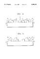
- FIG. 1is a cross-sectional view of a representative lithographic template.
- FIG. 2is a top view of a lithographic template undergoing the process of a preferred embodiment of the invention.
- FIG. 3is a side view of the template of FIG. 2.
- FIG. 4shows the template of FIG. 2 at a processing step subsequent to that shown in FIGS. 2 and 3.
- FIG. 5shows the template of FIG. 2 at a processing step subsequent to that shown in FIG. 4.
- the lithographic template 20may be a photomask, x-ray mask, reticle, or other similar structure having similar features.
- the lithographic templatecomprises a transparent substrate 22, an opaque portion 24 formed and patterned on the transparent substrate 22, and light transmitting portions 26 and 28.
- the transparent substrate 22is made of silica glass, fused silica, borosilicate glass, quartz, or the like, and is typically a 6 by 6 inch square having a thickness of approximately 0.25 inches, although the size and thickness may vary.
- the opaque portion 24is typically made of a chromium-containing material such as chromium oxide or chrome.
- the depth of the light transmitting portion 28is adjusted depending on the composition of the light transmitting portion 28 so that phase shifting within the range of 160 to 200 degrees is achieved.
- the phase shifting amountis 180 degrees.
- a lithographic template 20 having a quartz bump defect 30 thereonis shown in FIGS. 2 and 3.
- a "quartz bump”may be a bump of quartz, glass, silica or other silicate material.
- the template 20is placed in the vacuum chamber (not shown) of a FIB system.
- Any suitable FIB systemmay be utilized, as may a combination of a scanning electron microscope (SEM) and a FIB system.
- SEMscanning electron microscope
- the system or combinationshould be capable of low energy scanning at approximately a few KeV to 30 KeV, and high energy sputtering at approximately 90 to 130 KeV. If a FIB system is used, the low energy beam for imaging minimizes Ga + stains.
- scanningis performed to locate a quartz bump defect 30 on the template 20.
- Scanningmay be performed by a FIB system at a low energy of approximately a few to 30 KeV, or by an SEM.
- a high energy gallium FIBis directed at the bump 30, and sputtering is begun.
- most of the quartz bumpshave about an 80 nm height due to the design of the phase shifting mask manufacturing process. Due to the high energy, i.e., about 90 to 110 KeV, the ion beam penetrates approximately 80 nm into the surface of the quartz bump 30, thus permitting rapid gallium staining of the bump 30.
- the stained bump 30is then removed by exposing the template 20 to an aqueous solution of a strong base.
- Suitable basesinclude sodium hydroxide, potassium hydroxide, ammonium hydroxide, tetramethyl ammonium hydroxide, and the like.
- sodium hydroxideis used.
- the solutionshould comprise approximately 3 to 4 percent sodium hydroxide in water, or should be of an equivalent strength if another base is used.
- the sodium hydroxide solutionis heated to a temperature of approximately 75 to 85 degrees Celsius, and the template is exposed to this solution by wet etching means such as immersion or spray etching, for a period of time within the range of approximately 1 to 10 minutes.
- the temperatureis approximately 80 degrees.
- the exposure timewill vary according to the strength of the basic solution utilized. Due to the gallium staining of the bump 30, the material of the bump 30 is etched at a rate approximately four to five times as fast as the etching of the material of the template substrate 22. As can be seen in FIG. 5, the bump 30 has been removed from the surface of the template 20.
- the present inventionencompasses a quartz bump defect repair method for a lithographic template.
- the methoduses focused ion beam scanning to implant gallium ions into a quartz bump, followed by a treatment with a strong base such as sodium hydroxide to remove the stained bump.
- This processhas the advantage of avoiding the formation of riverbeds and reducing the undesirable effects of beam drift during the FIB process.
Landscapes
- Physics & Mathematics (AREA)
- General Physics & Mathematics (AREA)
- Preparing Plates And Mask In Photomechanical Process (AREA)
Abstract
Description
Claims (31)
Priority Applications (1)
| Application Number | Priority Date | Filing Date | Title |
|---|---|---|---|
| US09/220,893US6096459A (en) | 1998-12-28 | 1998-12-28 | Method for repairing alternating phase shifting masks |
Applications Claiming Priority (1)
| Application Number | Priority Date | Filing Date | Title |
|---|---|---|---|
| US09/220,893US6096459A (en) | 1998-12-28 | 1998-12-28 | Method for repairing alternating phase shifting masks |
Publications (1)
| Publication Number | Publication Date |
|---|---|
| US6096459Atrue US6096459A (en) | 2000-08-01 |
Family
ID=22825447
Family Applications (1)
| Application Number | Title | Priority Date | Filing Date |
|---|---|---|---|
| US09/220,893Expired - LifetimeUS6096459A (en) | 1998-12-28 | 1998-12-28 | Method for repairing alternating phase shifting masks |
Country Status (1)
| Country | Link |
|---|---|
| US (1) | US6096459A (en) |
Cited By (10)
| Publication number | Priority date | Publication date | Assignee | Title |
|---|---|---|---|---|
| US6346352B1 (en)* | 2000-02-25 | 2002-02-12 | International Business Machines Corporation | Quartz defect removal utilizing gallium staining and femtosecond ablation |
| US20020121109A1 (en)* | 2000-12-21 | 2002-09-05 | Kazuo Aita | Glass substrate processing method |
| US6580172B2 (en)* | 2001-03-02 | 2003-06-17 | Motorola, Inc. | Lithographic template and method of formation and use |
| US20030215721A1 (en)* | 2002-05-15 | 2003-11-20 | Baorui Yang | Method for quartz bump defect repair with less substrate damage |
| US20040131953A1 (en)* | 2002-11-27 | 2004-07-08 | Yasuhiko Sugiyama | Photomask correction method using composite charged particle beam, and device used in the correction method |
| US20040175631A1 (en)* | 2002-10-21 | 2004-09-09 | Nanoink, Inc. | Nanometer-scale engineered structures, methods and apparatus for fabrication thereof, and applications to mask repair, enhancement, and fabrications |
| US20050214653A1 (en)* | 2004-03-26 | 2005-09-29 | Ming Lu | Repair of photolithography masks by sub-wavelength artificial grating technology |
| NL1024729C2 (en)* | 2002-11-07 | 2006-09-14 | Infineon Technologies Ag | Method for repairing a photolithographic mask and a photolithographic mask. |
| US20070293052A1 (en)* | 2005-02-24 | 2007-12-20 | Credence Systems Corporation | Apparatus and method for optical interference fringe based integrated circuit processing |
| JP2016082189A (en)* | 2014-10-22 | 2016-05-16 | 大日本印刷株式会社 | A method for correcting a mask for nanoimprint lithography and a method for manufacturing a mask for nanoimprint lithography. |
Citations (16)
| Publication number | Priority date | Publication date | Assignee | Title |
|---|---|---|---|---|
| US4851097A (en)* | 1986-12-26 | 1989-07-25 | Seiko Instruments Inc. | Apparatus for repairing a pattern film |
| US5035787A (en)* | 1987-07-22 | 1991-07-30 | Microbeam, Inc. | Method for repairing semiconductor masks and reticles |
| US5085957A (en)* | 1990-04-18 | 1992-02-04 | Mitsubishi Denki Kabushiki Kaisha | Method of repairing a mask |
| US5165954A (en)* | 1986-09-02 | 1992-11-24 | Microbeam, Inc. | Method for repairing semiconductor masks & reticles |
| US5246801A (en)* | 1991-09-20 | 1993-09-21 | At&T Bell Laboratories | Method of repairing indentations in phase-shifting lithographic masks |
| US5272116A (en)* | 1991-11-18 | 1993-12-21 | Mitsubishi Denki Kabushiki Kaisha | Method for pattern defect correction of a photomask |
| US5357116A (en)* | 1992-11-23 | 1994-10-18 | Schlumberger Technologies, Inc. | Focused ion beam processing with charge control |
| US5382484A (en)* | 1992-08-21 | 1995-01-17 | Mitsubishi Denki Kabushiki Kaisha | Method of correcting defects in the pattern of phase shift mask |
| US5405721A (en)* | 1992-08-18 | 1995-04-11 | At&T Corp. | Phase-shifting lithographic masks having phase-shifting layers of differing compositions |
| US5576126A (en)* | 1994-09-26 | 1996-11-19 | Micron Technology, Inc. | Phase shifting mask |
| US5582939A (en)* | 1995-07-10 | 1996-12-10 | Micron Technology, Inc. | Method for fabricating and using defect-free phase shifting masks |
| US5635315A (en)* | 1995-06-21 | 1997-06-03 | Hoya Corporation | Phase shift mask and phase shift mask blank |
| US5695896A (en)* | 1995-12-04 | 1997-12-09 | Micron Technology, Inc. | Process for fabricating a phase shifting mask |
| US5759724A (en)* | 1997-03-31 | 1998-06-02 | Micron Technology, Inc. | Method for making multi-phase, phase shifting masks |
| US5795685A (en)* | 1997-01-14 | 1998-08-18 | International Business Machines Corporation | Simple repair method for phase shifting masks |
| US5965301A (en)* | 1996-11-26 | 1999-10-12 | Dai Nippon Printing Co., Ltd. | Method for repairing photomask by removing residual defect in said photomask |
- 1998
- 1998-12-28USUS09/220,893patent/US6096459A/ennot_activeExpired - Lifetime
Patent Citations (16)
| Publication number | Priority date | Publication date | Assignee | Title |
|---|---|---|---|---|
| US5165954A (en)* | 1986-09-02 | 1992-11-24 | Microbeam, Inc. | Method for repairing semiconductor masks & reticles |
| US4851097A (en)* | 1986-12-26 | 1989-07-25 | Seiko Instruments Inc. | Apparatus for repairing a pattern film |
| US5035787A (en)* | 1987-07-22 | 1991-07-30 | Microbeam, Inc. | Method for repairing semiconductor masks and reticles |
| US5085957A (en)* | 1990-04-18 | 1992-02-04 | Mitsubishi Denki Kabushiki Kaisha | Method of repairing a mask |
| US5246801A (en)* | 1991-09-20 | 1993-09-21 | At&T Bell Laboratories | Method of repairing indentations in phase-shifting lithographic masks |
| US5272116A (en)* | 1991-11-18 | 1993-12-21 | Mitsubishi Denki Kabushiki Kaisha | Method for pattern defect correction of a photomask |
| US5405721A (en)* | 1992-08-18 | 1995-04-11 | At&T Corp. | Phase-shifting lithographic masks having phase-shifting layers of differing compositions |
| US5382484A (en)* | 1992-08-21 | 1995-01-17 | Mitsubishi Denki Kabushiki Kaisha | Method of correcting defects in the pattern of phase shift mask |
| US5357116A (en)* | 1992-11-23 | 1994-10-18 | Schlumberger Technologies, Inc. | Focused ion beam processing with charge control |
| US5576126A (en)* | 1994-09-26 | 1996-11-19 | Micron Technology, Inc. | Phase shifting mask |
| US5635315A (en)* | 1995-06-21 | 1997-06-03 | Hoya Corporation | Phase shift mask and phase shift mask blank |
| US5582939A (en)* | 1995-07-10 | 1996-12-10 | Micron Technology, Inc. | Method for fabricating and using defect-free phase shifting masks |
| US5695896A (en)* | 1995-12-04 | 1997-12-09 | Micron Technology, Inc. | Process for fabricating a phase shifting mask |
| US5965301A (en)* | 1996-11-26 | 1999-10-12 | Dai Nippon Printing Co., Ltd. | Method for repairing photomask by removing residual defect in said photomask |
| US5795685A (en)* | 1997-01-14 | 1998-08-18 | International Business Machines Corporation | Simple repair method for phase shifting masks |
| US5759724A (en)* | 1997-03-31 | 1998-06-02 | Micron Technology, Inc. | Method for making multi-phase, phase shifting masks |
Non-Patent Citations (4)
| Title |
|---|
| Seiko Instrument, Inc. Scientific Instrument Division, SIR 3000, Photomask Repair System, Operation Manual.* |
| Seiko Instrument, Inc. Scientific Instrument Division, SIR-3000, Photomask Repair System, Operation Manual. |
| Y. Satoh et al., "Performance of Gas Assist FIB Repair for Opaque Defects", SPIE, vol. 2884, pp. 124-137. |
| Y. Satoh et al., Performance of Gas Assist FIB Repair for Opaque Defects , SPIE, vol. 2884, pp. 124 137.* |
Cited By (17)
| Publication number | Priority date | Publication date | Assignee | Title |
|---|---|---|---|---|
| US6346352B1 (en)* | 2000-02-25 | 2002-02-12 | International Business Machines Corporation | Quartz defect removal utilizing gallium staining and femtosecond ablation |
| US20020121109A1 (en)* | 2000-12-21 | 2002-09-05 | Kazuo Aita | Glass substrate processing method |
| US6580172B2 (en)* | 2001-03-02 | 2003-06-17 | Motorola, Inc. | Lithographic template and method of formation and use |
| US20070105027A1 (en)* | 2002-05-15 | 2007-05-10 | Baorui Yang | Method for quartz bump defect repair with less substrate damage |
| US20030215721A1 (en)* | 2002-05-15 | 2003-11-20 | Baorui Yang | Method for quartz bump defect repair with less substrate damage |
| US6933081B2 (en)* | 2002-05-15 | 2005-08-23 | Micron Technology, Inc. | Method for quartz bump defect repair with less substrate damage |
| US7569314B2 (en) | 2002-05-15 | 2009-08-04 | Micron Technology, Inc. | Method for quartz bump defect repair with less substrate damage |
| US20040175631A1 (en)* | 2002-10-21 | 2004-09-09 | Nanoink, Inc. | Nanometer-scale engineered structures, methods and apparatus for fabrication thereof, and applications to mask repair, enhancement, and fabrications |
| US7691541B2 (en) | 2002-10-21 | 2010-04-06 | Nanoink, Inc. | Methods for additive repair of phase shift masks by selectively depositing nanometer-scale engineered structures on defective phase shifters |
| NL1024729C2 (en)* | 2002-11-07 | 2006-09-14 | Infineon Technologies Ag | Method for repairing a photolithographic mask and a photolithographic mask. |
| US20040131953A1 (en)* | 2002-11-27 | 2004-07-08 | Yasuhiko Sugiyama | Photomask correction method using composite charged particle beam, and device used in the correction method |
| US7172839B2 (en)* | 2002-11-27 | 2007-02-06 | Sii Nanotechnology Inc. | Photomask correction method using composite charged particle beam, and device used in the correction method |
| US7303841B2 (en) | 2004-03-26 | 2007-12-04 | Taiwan Semiconductor Manufacturing Company | Repair of photolithography masks by sub-wavelength artificial grating technology |
| US20050214653A1 (en)* | 2004-03-26 | 2005-09-29 | Ming Lu | Repair of photolithography masks by sub-wavelength artificial grating technology |
| US20070293052A1 (en)* | 2005-02-24 | 2007-12-20 | Credence Systems Corporation | Apparatus and method for optical interference fringe based integrated circuit processing |
| US7884024B2 (en)* | 2005-02-24 | 2011-02-08 | Dcg Systems, Inc. | Apparatus and method for optical interference fringe based integrated circuit processing |
| JP2016082189A (en)* | 2014-10-22 | 2016-05-16 | 大日本印刷株式会社 | A method for correcting a mask for nanoimprint lithography and a method for manufacturing a mask for nanoimprint lithography. |
Similar Documents
| Publication | Publication Date | Title |
|---|---|---|
| US6335129B1 (en) | Method for repairing pattern defect, photo mask using the method, and semiconductor device manufacturing method employing the photo mask | |
| US7569314B2 (en) | Method for quartz bump defect repair with less substrate damage | |
| JPH10161293A (en) | Photomask residual defect repair method | |
| US7090948B2 (en) | Reflection mask and method for fabricating the reflection mask | |
| US6447962B2 (en) | Method for repairing MoSi attenuated phase shift masks | |
| JP2001249440A (en) | Removal of quartz defect using gallium dyeing and femtosecond peeling | |
| US6096459A (en) | Method for repairing alternating phase shifting masks | |
| US6114073A (en) | Method for repairing phase shifting masks | |
| US6030731A (en) | Method for removing the carbon halo caused by FIB clear defect repair of a photomask | |
| KR19990072347A (en) | Method for repairing photomasks | |
| JP5012952B2 (en) | Photomask defect correction method | |
| JP4426730B2 (en) | Mask black defect correction method | |
| JP3732118B2 (en) | Opaque defect repair method for photomask for opening | |
| JP4926383B2 (en) | Photomask defect correction method | |
| US20060199082A1 (en) | Mask repair | |
| Saitoh et al. | Practical results of photomask repair using focused ion beam technology | |
| KR100298175B1 (en) | Method for fabricating photomask | |
| KR100314128B1 (en) | Method for repairing a defect of photomask | |
| JPH05303190A (en) | PHASE-SHIFT PHOTOMASK AND METHOD OF MANUFACTURING THE SAME | |
| JP2000029201A (en) | Phase shift mask repair method and phase shift mask repair apparatus | |
| KR20000004744A (en) | Defect Tree Pairing Method of Phase Inversion Mask | |
| JP2000100714A (en) | How to repair a stencil type reticle | |
| JP2003121991A (en) | Photomask white defect repair method | |
| JP2003084422A (en) | Method for correcting halftone type phase shift mask, phase shift mask and method for manufacturing the same | |
| JP2003318093A (en) | Method for manufacturing mask and method for manufacturing semiconductor device |
Legal Events
| Date | Code | Title | Description |
|---|---|---|---|
| AS | Assignment | Owner name:MICRON TECHNOLOGY, INC., IDAHO Free format text:ASSIGNMENT OF ASSIGNORS INTEREST;ASSIGNOR:YANG, BAORUI;REEL/FRAME:009684/0896 Effective date:19981207 | |
| STCF | Information on status: patent grant | Free format text:PATENTED CASE | |
| FPAY | Fee payment | Year of fee payment:4 | |
| FEPP | Fee payment procedure | Free format text:PAYOR NUMBER ASSIGNED (ORIGINAL EVENT CODE: ASPN); ENTITY STATUS OF PATENT OWNER: LARGE ENTITY Free format text:PAYER NUMBER DE-ASSIGNED (ORIGINAL EVENT CODE: RMPN); ENTITY STATUS OF PATENT OWNER: LARGE ENTITY | |
| FPAY | Fee payment | Year of fee payment:8 | |
| FPAY | Fee payment | Year of fee payment:12 | |
| AS | Assignment | Owner name:U.S. BANK NATIONAL ASSOCIATION, AS COLLATERAL AGENT, CALIFORNIA Free format text:SECURITY INTEREST;ASSIGNOR:MICRON TECHNOLOGY, INC.;REEL/FRAME:038669/0001 Effective date:20160426 Owner name:U.S. BANK NATIONAL ASSOCIATION, AS COLLATERAL AGEN Free format text:SECURITY INTEREST;ASSIGNOR:MICRON TECHNOLOGY, INC.;REEL/FRAME:038669/0001 Effective date:20160426 | |
| AS | Assignment | Owner name:MORGAN STANLEY SENIOR FUNDING, INC., AS COLLATERAL AGENT, MARYLAND Free format text:PATENT SECURITY AGREEMENT;ASSIGNOR:MICRON TECHNOLOGY, INC.;REEL/FRAME:038954/0001 Effective date:20160426 Owner name:MORGAN STANLEY SENIOR FUNDING, INC., AS COLLATERAL Free format text:PATENT SECURITY AGREEMENT;ASSIGNOR:MICRON TECHNOLOGY, INC.;REEL/FRAME:038954/0001 Effective date:20160426 | |
| AS | Assignment | Owner name:U.S. BANK NATIONAL ASSOCIATION, AS COLLATERAL AGENT, CALIFORNIA Free format text:CORRECTIVE ASSIGNMENT TO CORRECT THE REPLACE ERRONEOUSLY FILED PATENT #7358718 WITH THE CORRECT PATENT #7358178 PREVIOUSLY RECORDED ON REEL 038669 FRAME 0001. ASSIGNOR(S) HEREBY CONFIRMS THE SECURITY INTEREST;ASSIGNOR:MICRON TECHNOLOGY, INC.;REEL/FRAME:043079/0001 Effective date:20160426 Owner name:U.S. BANK NATIONAL ASSOCIATION, AS COLLATERAL AGEN Free format text:CORRECTIVE ASSIGNMENT TO CORRECT THE REPLACE ERRONEOUSLY FILED PATENT #7358718 WITH THE CORRECT PATENT #7358178 PREVIOUSLY RECORDED ON REEL 038669 FRAME 0001. ASSIGNOR(S) HEREBY CONFIRMS THE SECURITY INTEREST;ASSIGNOR:MICRON TECHNOLOGY, INC.;REEL/FRAME:043079/0001 Effective date:20160426 | |
| AS | Assignment | Owner name:JPMORGAN CHASE BANK, N.A., AS COLLATERAL AGENT, ILLINOIS Free format text:SECURITY INTEREST;ASSIGNORS:MICRON TECHNOLOGY, INC.;MICRON SEMICONDUCTOR PRODUCTS, INC.;REEL/FRAME:047540/0001 Effective date:20180703 Owner name:JPMORGAN CHASE BANK, N.A., AS COLLATERAL AGENT, IL Free format text:SECURITY INTEREST;ASSIGNORS:MICRON TECHNOLOGY, INC.;MICRON SEMICONDUCTOR PRODUCTS, INC.;REEL/FRAME:047540/0001 Effective date:20180703 | |
| AS | Assignment | Owner name:MICRON TECHNOLOGY, INC., IDAHO Free format text:RELEASE BY SECURED PARTY;ASSIGNOR:U.S. BANK NATIONAL ASSOCIATION, AS COLLATERAL AGENT;REEL/FRAME:047243/0001 Effective date:20180629 | |
| AS | Assignment | Owner name:MICRON TECHNOLOGY, INC., IDAHO Free format text:RELEASE BY SECURED PARTY;ASSIGNOR:MORGAN STANLEY SENIOR FUNDING, INC., AS COLLATERAL AGENT;REEL/FRAME:050937/0001 Effective date:20190731 | |
| AS | Assignment | Owner name:MICRON TECHNOLOGY, INC., IDAHO Free format text:RELEASE BY SECURED PARTY;ASSIGNOR:JPMORGAN CHASE BANK, N.A., AS COLLATERAL AGENT;REEL/FRAME:051028/0001 Effective date:20190731 Owner name:MICRON SEMICONDUCTOR PRODUCTS, INC., IDAHO Free format text:RELEASE BY SECURED PARTY;ASSIGNOR:JPMORGAN CHASE BANK, N.A., AS COLLATERAL AGENT;REEL/FRAME:051028/0001 Effective date:20190731 |