US6094285A - All optical RF signal channelizer - Google Patents
All optical RF signal channelizerDownload PDFInfo
- Publication number
- US6094285A US6094285AUS08/759,901US75990196AUS6094285AUS 6094285 AUS6094285 AUS 6094285AUS 75990196 AUS75990196 AUS 75990196AUS 6094285 AUS6094285 AUS 6094285A
- Authority
- US
- United States
- Prior art keywords
- optical
- signals
- channelizer
- channels
- signal
- Prior art date
- Legal status (The legal status is an assumption and is not a legal conclusion. Google has not performed a legal analysis and makes no representation as to the accuracy of the status listed.)
- Expired - Lifetime
Links
- 230000003287optical effectEffects0.000titleclaimsabstractdescription113
- VYPSYNLAJGMNEJ-UHFFFAOYSA-NSilicium dioxideChemical compoundO=[Si]=OVYPSYNLAJGMNEJ-UHFFFAOYSA-N0.000claimsabstractdescription32
- 239000000377silicon dioxideSubstances0.000claimsabstractdescription16
- LFEUVBZXUFMACD-UHFFFAOYSA-Hlead(2+);trioxido(oxo)-$l^{5}-arsaneChemical compound[Pb+2].[Pb+2].[Pb+2].[O-][As]([O-])([O-])=O.[O-][As]([O-])([O-])=OLFEUVBZXUFMACD-UHFFFAOYSA-H0.000claimsabstractdescription15
- 230000001427coherent effectEffects0.000claimsdescription2
- 238000013507mappingMethods0.000abstractdescription3
- 238000001914filtrationMethods0.000abstractdescription2
- 238000001228spectrumMethods0.000description15
- 238000004891communicationMethods0.000description11
- 238000000926separation methodMethods0.000description8
- 238000000034methodMethods0.000description7
- 230000003595spectral effectEffects0.000description7
- 230000001934delayEffects0.000description6
- 238000010586diagramMethods0.000description6
- 239000006185dispersionSubstances0.000description6
- 238000005516engineering processMethods0.000description6
- 230000035559beat frequencyEffects0.000description4
- 239000000835fiberSubstances0.000description4
- 238000003491arrayMethods0.000description3
- 230000005540biological transmissionEffects0.000description3
- 238000013461designMethods0.000description3
- 238000003384imaging methodMethods0.000description3
- 238000001514detection methodMethods0.000description2
- 230000005684electric fieldEffects0.000description2
- 230000007062hydrolysisEffects0.000description2
- 238000006460hydrolysis reactionMethods0.000description2
- 238000004519manufacturing processMethods0.000description2
- 238000001020plasma etchingMethods0.000description2
- 230000010287polarizationEffects0.000description2
- 238000012545processingMethods0.000description2
- 238000010183spectrum analysisMethods0.000description2
- 229910000980Aluminium gallium arsenideInorganic materials0.000description1
- 229910001218Gallium arsenideInorganic materials0.000description1
- XUIMIQQOPSSXEZ-UHFFFAOYSA-NSiliconChemical compound[Si]XUIMIQQOPSSXEZ-UHFFFAOYSA-N0.000description1
- 230000008021depositionEffects0.000description1
- 238000002347injectionMethods0.000description1
- 239000007924injectionSubstances0.000description1
- 238000002156mixingMethods0.000description1
- 238000012986modificationMethods0.000description1
- 230000004048modificationEffects0.000description1
- 239000013307optical fiberSubstances0.000description1
- 238000005086pumpingMethods0.000description1
- 229910052710siliconInorganic materials0.000description1
- 239000010703siliconSubstances0.000description1
- 238000010561standard procedureMethods0.000description1
- 239000000758substrateSubstances0.000description1
- 238000012546transferMethods0.000description1
- 230000004304visual acuityEffects0.000description1
Images


Classifications
- H—ELECTRICITY
- H04—ELECTRIC COMMUNICATION TECHNIQUE
- H04B—TRANSMISSION
- H04B10/00—Transmission systems employing electromagnetic waves other than radio-waves, e.g. infrared, visible or ultraviolet light, or employing corpuscular radiation, e.g. quantum communication
- H04B10/60—Receivers
- H04B10/66—Non-coherent receivers, e.g. using direct detection
- H04B10/67—Optical arrangements in the receiver
- H04B10/671—Optical arrangements in the receiver for controlling the input optical signal
- H—ELECTRICITY
- H04—ELECTRIC COMMUNICATION TECHNIQUE
- H04B—TRANSMISSION
- H04B10/00—Transmission systems employing electromagnetic waves other than radio-waves, e.g. infrared, visible or ultraviolet light, or employing corpuscular radiation, e.g. quantum communication
- H04B10/25—Arrangements specific to fibre transmission
- H04B10/2575—Radio-over-fibre, e.g. radio frequency signal modulated onto an optical carrier
- H—ELECTRICITY
- H04—ELECTRIC COMMUNICATION TECHNIQUE
- H04B—TRANSMISSION
- H04B2210/00—Indexing scheme relating to optical transmission systems
- H04B2210/006—Devices for generating or processing an RF signal by optical means
Definitions
- the present inventionrelates to a channelizer for RF signals and more particularly to an optical RF channelizer, for example, for use for RF spectral analysis, for optically channelizing RF signals modulated onto an optical carrier by optically separating the RF spectrum.
- Optical channelizersare used to perform spectral analysis of the newer high frequency communication signals. Such optical channelizers are known to process relatively wider bandwidths than comparable RF channelizers for real time identification of complex signals. Examples of such optical channelizers are disclosed in U.S. Pat. Nos. 4,460,250 and 4,695,795 and U.S. Statutory Invention Registration H1059. Such channelizers are used to channelize or divide up a relatively wide bandwidth signal into several sub-bands or channels. Such optical channelizers are known to process relatively wider bandwidths than known RF channelizers. However, many of the optical channelizers utilize acousto-optic technology and thus are limited to RF bandwidths of a few GHz. Examples of optical communication systems utilizing acousto-optic technology are disclosed in U.S. Pat. No. 4,448,494; 4,644,267; 5,005,946; 5,105,380; 5,327,142; and 5,363,221.
- the channelizingis done in the RF band.
- the RF signalis demodulated from the optical carrier and greatly amplified in order to achieve channelization.
- the present inventionrelates to a channelizer for RF signals and more particularly to a RF channelizer for optically channelizing RF signals modulated onto an optical carrier by optically separating or mapping the RF spectrum by way of an optically dispersive element, such as a conventional diffraction grating, or a silica planar waveguide tapped delay line.
- an optically dispersive elementsuch as a conventional diffraction grating, or a silica planar waveguide tapped delay line.
- two stages of optical filters elementsare provided in series to perform sequential channelization. Bragg reflection gratings are used for coarse filtering into 3-4 GHz bands while Fabry-Perot filters tuned to specific sub-bands of the Bragg reflection grating is used for channelization.
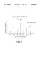
- FIG. 1is a frequency diagram of optical wavelength vs. optical amplitude illustrating an optical carrier and RF sidebands.
- FIG. 2is a diagram of an all optical channelizer in accordance with the present invention.
- FIG. 3is a diagram illustrating heterodyne optical separation in accordance with the present invention.
- FIG. 4is a diagram of an alternate embodiment of the all optical channelizer illustrated in FIG. 2.
- FIG. 5is a diagram of a waveguide implementation with incremental time delays for use with the present invention.
- FIG. 6is a diagram of a Talbot splitter for use with the present invention.
- FIG. 7is a perspective view of an optical channelizer in accordance with the present invention, illustrating the use of a triple grating.
- the present inventionrelates to an optical channelizer for channelizing relatively wide band high frequency RF communication signals.
- the channelizingis done optically without utilizing an acousto-opto coupler device.
- the systemallows for signal processing and in particular, channelizing of RF signals having frequencies, for example, up to 100 GHz.
- the resulting optical spectrumreplicates the input RF signals.
- the RF signalsis upconverted to optical frequencies, wherein the RF signals are represented by sidebands on the optical carrier with an optical frequency offset and amplitude corresponding to the RF frequency and amplitude.
- the optical amplitudeis illustrated on the vertical axis while the optical wavelength is shown on the horizontal axis.
- the optical carrier frequencyis shown at a wavelength of T0.
- Exemplary RF frequencies T1, T2 and T3are represented by sidebands relative to the optical carrier frequency T0.
- optical heterodyningmay be used to downconvert the modulated optical signals to a common RF frequency so that the channels of the RF modulated optical carrier can be utilized with a detector optimized for a single frequency. The heterodyning allows both phase and amplitude to be recovered from the original RF signals.
- the demodulated RF voltage waveform in any one channelis proportional to the product of the local oscillator field (ELO) and the signal field (Es). Since this waveform is proportional to the input voltage waveform, the optical modulator transmits an electric field amplitude that is linear with input voltage. Since electric field is proportional to the square root of optical amplitude, an ideal characteristic is one that transmits an amplitude proportional to the square of the input voltage.
- ELOlocal oscillator field
- Essignal field
- the modulation transfer characteristicis quadratic
- the current waveform generated in the photodetectorreverts to a true representation of the ideal signal.
- a Mach-Zehnder interferometric modulatormay be used and operated at a low bias point. Under such modulation conditions, known second order inter-modulation products are minimized while the dynamic range is maximized.
- FIGS. 2 and 3Multiple embodiments of the invention are disclosed for channelization of RF spectrum signals.
- the first embodiment, illustrated in FIGS. 2 and 3,utilizes a dispersive element, such as a spatial dispersion grating
- the second embodiment illustrated in FIG. 4utilizes a sequence of fiber optic Fabry-Perot filters and fiber optic Bragg gratings.
- FIGS. 5 and 6represent embodiments that are amenable to monolithic fabrication.
- FIG. 6illustrates an embodiment utilizing a Talbot splitter.
- a diffraction gratingis used as a spatially dispersive element to channelize the RF spectrum in a single parallel operation.
- RF input signalsare input to an RF-optical modulation device 20, such as a diode laser or an electroabsorptive modulator or preferably, as discussed above, a Mach-Zehnder interferometer.
- the modulator 20generates the optical spectrum as illustrated in FIG. 1.
- the optical signal from the modulator 20is impinged on a dispersive element 22, such as a conventional high dispersion diffraction grating, such as a echelle, blazed for high optical diffraction efficiency.
- the angular dispersionresults in a spatial separation or mapping of the optical frequencies i.e. separation of the RF sidebands onto the optical carrier.
- One or more detector arrays 24, 25, for example, linear detector arraysare spaced a distance away from the dispersive element 22 to receive the dispersed optical signals.
- Each of the detector elements in the linear detector arrays, 24 and 25receives an optical signal with an amplitude proportional to the RF power. As shown, the detector array 25 can be used to improve signal to noise ratio.
- heterodyningis used to downconvert an optical signal to a common RF frequency so that the separated portions or channels of the RF modulated optical carrier can utilize a detector optimized for a single frequency.
- the local oscillators used for the heterodyningcan be generated by a mode-locked laser which provides a set of phase coherent monochromatic optical sources separated in frequency by a common interval equal to the desired channel spacing to allow both phase and amplitude to be recovered from the original RF signals. As shown in FIG.
- a mode-locked laser, used as an optical local oscillator, represented by the line 26,is directed to the dispersive element 22; however, the local oscillator signals 26 are injected onto the dispersive element at a slightly different angle than the signal laser, represented by the line 28, to define an IF frequency.
- the mode locked laser 26provides a comb of optical oscillators whose frequencies are separated by the desired channel spacing. The spectral components of the dispersed RF signal laser and the comb of frequencies generated by the mode-locked laser are combined at the detector location 24, 25, which may either, for example, a linear detector array.
- Each portion or channel of the modulated signal laser and one component of the frequency comb at each detector sitewill have a frequency offset which can serve as the heterodyne frequency which can be adjusted by varying the injection angle offset to the dispersive elements.
- each photodetectorgenerates the same optical beat frequency so that each detector channel can use the same post detection electronics.
- the IF beat frequencycan be tuned by adjusting the offset in incident angles at which the signal and local oscillator lasers are impinged on the dispersive element 22.
- the beat frequencycan be adjusted to be equal to the channelized bandwidth to allow the use of relatively slow photodetectors even for channels corresponding to very high RF signal frequencies.
- the signal power spectrumis determined by measuring the RF power of the heterodyne products generated in each photodetector channel.
- the complex signal spectrum, both phase and amplitude,can be extracted by measuring the inphase and quadrature components of the heterodyne products.
- gratingsare suitable for use for the embodiment illustrated in FIGS. 2 and 3.
- a more compact systemcan be based upon the standard technique of multiple diffraction passes. For example, a triple pass grating design with the same frequency resolution with diffraction gratings approximately 5" to 6" in size. Since the beam pass for the signal and local oscillator effectively see each of the three gratings in series, the net dispersion is tripled. This allows the focal length to be reduced to 1/3 of the single grating design.
- a channel spacing of one GHzoptical wavelength and below 0.008 nanometers
- a focal plane element spacing of 10 micronsa 0.7 meter focal length system is required; however, the optical paths may be folded to make the system more compact.
- the entire 100 GHz spectrumspans an angular size of 0.991 microradians which translates to a focal plane array length of 2.2 millimeters.
- the triple pass systemfor example, as illustrated in FIG. 7, can be used to reduce the focal length to 0.7 meters divided by 3 (i.e., 24 centimeters.
- two stages of optical filter elementsare used in series to perform sequential bandwidth channelization.
- Bragg reflection gratings 31, 33are used for coarse prefiltering of the optically carried RF spectrum into predetermined optical bands, for example 3GHz.
- Channel pick offmay be achieved using a sequence of channel pick-off devices, such as polarizing beam splitters 30, 32, 34, 36, 38, 40 and 42 and Faraday rotators 44, 46, 48 and 50.
- the bandsare filtered into higher resolution sub-bands by way of chains of Fabry-Perot reflection filters 52, 54, 56 and 58 and corresponding quarter wave plates 60, 62, 64 and 66.
- Each Fabry-Perot reflection filter 52, 54, 56 and 58is tuned to transmit a specific sub-band of the 3 GHz Bragg grating 31, 33 band. All remaining sub-bands are reflected and transmitted through the rest of the Fabry-Perot chain to complete the channelization of the Bragg grating band.
- Local oscillatorsare channelized using a Bragg grating series similar to that used to channelize a signal laser. 3 GHz local oscillator bands are combined with the 3 GHz signal laser bands at the Fabry-Perot chain inputs but offset by one Bragg grating band to generate an IF beat frequency.
- the Fabry-Perot free spectral rangeis set equal to the Bragg grating bandwidths so that the local oscillator and the signal bands can pass through a common Fabry-Perot chain.
- the local oscillatorsare the stronger of the signals so that Fabry-Perot transmission peaks are locked to the local oscillator frequencies in the closed loop mode.
- Both the Bragg filter and Fabry-Perot filter chainssection the bands of the spectrum and send the rest of the spectrum down the filter chain for subsequent sectionizing without discarding any of the optical energy. Other than transmission losses, no energy is discarded.
- the Bragg filter chainuses polarization beam splitters and quarter wave Faraday rotators along with Bragg filters to distribute the sub-bands of the RF modulated optical spectrum.
- the Fabry-Perot chainuses 1/4 wave plates and polarization beam splitter to distribute the bands of the RF modulated optical spectrum into individual channels.
- the local oscillatorsare generated by a mode-locked laser.
- the local oscillatorsare filtered into coarse sub-bands with a Bragg grating series similar to, but separate from the signal laser. Any one local oscillator sub-band and signal laser sub-band are sent down one Fabry-Perot chain. However, the local oscillator sub-band and the signal sub-band are separated in frequency by the free spectral range of the Fabry-Perot devices.
- the free spectral rangedefines the intermediate frequency and is selectable.
- the channelizercan be formed on a small wafer, by utilizing the principles incorporated in a Michelson echelon.
- Very high resolving power with 1000 lines or elements in a large angular dispersioncan be achieved when operating in high order.
- the small free spectral range that results when working at high ordersis sufficient for the application.
- the large incremental time delay between lines or elements that results when operating at high orderis achieved with staggered stacked plates in a Michelson echelon, as generally shown is FIG. 5.
- FIG. 5illustrates single mode channels or waveguides 70 formed as a silica planar waveguide.
- a modulated signal carried on a single mode fiberis injected at port 1 and sequentially divided into individual waveguides with incrementally longer pathlengths.
- Such a device with incremental time delays of, for example, five picoseconds having 1000 elementswould have a resolution of 200 MHz and fit on a 5 centimeter wafer.
- Silica planar waveguides formed as silica based optical integrated circuits, as illustrated in FIG. 5,are generally known in the art and disclosed in "Silica-Based Integrated Optic Mach-Zehnder Multi/Demultiplexer Family with Channel Spacing of 0.01-250 nm" by N. Takato, T. Kominato, A. Sugita, K. Jinguji, H. Toba and M. Kawachi, IEEE Journal on Selected Areas in Communications, Vol. 8, No. 6, pps. 1120-1127, August 1990, hereby incorporated by reference.
- Such silica planar waveguidesare formed on a silica substrate 72 by flame hydrolysis deposition and conventional photolithographic techniques followed by reactive ion etching.
- Flame hydrolysisis based on optical fiber fabrication, while photolithographic and reactive ion etching processes are compatible with existing silicon technology as generally disclosed in "Silica-Based Single Mode Waveguides and Their Application to Guided-Wave Optical Interferometers", by N. Takato, K. Jinguji, M. Yasu, H. Toba and M. Kawachi, Journal of Lichtwave Technology, Vol. 6, pp. 1003-1010, 1988 and "Low-Loss High Silica Single Mode Channel Waveguides", by N. Takato, M. Yasu and M. Kawachi, Electron. Lett., Vol. 22, pp. 321-322, 1986, hereby incorporated by reference.
- Such silica planar waveguidescan be formed in various configurations with a relatively high degree of accuracy using the processes discussed above.
- the silica planar waveguide 70 illustrated in FIG. 5can be formed with 100-1000 waveguide channels 74-84 or more.
- Each waveguide channelis incrementally longer (i.e., has a longer path length) than the previous channel.
- the waveguide channel 76is longer than the waveguide channel 74; the waveguide channel 78 is incrementally longer than the waveguide channel 76, etc.
- the differences in lengths of the waveguide channels 74-84result in incremental delays at the detector array 86, thus emulating a diffraction grating.
- silica planar waveguide 70has virtually no limitations with respect to the highest order at which the device can be effectively operated.
- the silica planar waveguide 70allows extremely high order devices to be used to improve resolution (i.e., number of channels multiplied by the order) without increasing the number of channels.
- An alternative method for splitting the signal into a plurality of componentsis an optical splitter device, such as Talbot splitter as illustrated in FIG. 6.
- the Talbot splitteris based on multimode self imaging.
- a 1 ⁇ 32 Talbot splitter followed by 32 cascading one by 32 splitterswould provide 1,024 elements.
- the optical waveguidesfollow the Talbot splitters and provide the necessary incremental time delays.
- Optical gainis added by optically pumping regions of the waveguide incorporated under the same wafer as the channelizer including the mode-locked laser, signal laser, modulator, imaging lens and detector array.
- Talbot splittersare formed of beam splitters as generally disclosed in "Novel 1-to-N Way Integrated Optical Beam Splitters Using Symmetric Mode Mixing in GaAs/AlGaAs Multimode Waveguides", by J. M. Heatan, R. M. Jenkins, D. R. Wright, J. T. Parker, J. C. H. Birbeck and K. P. Hilton, Appl. Phys. Lett., Vol. 61, No. 15, pp. 1754-1756, 1992 and "Waveguide Beam Splitters and Recombiners Based on Multiple Propagation Phenomenon", by R. M. Jenkins, R. W. J. Devereux and J. M. Heaton, Optics Lett., Vol. 17, No.
- Each channel 88, 90, 92 and 94is optically coupled to a plurality of optical waveguides 96, 98, 100 and 102; wherein each waveguide is formed to be incrementally longer than a contiguous waveguide.
- the waveguide 100is formed to be incrementally longer than the contiguous waveguide 102
- the waveguide 98is formed to be incrementally longer than the contiguous waveguide 102, etc.
- the waveguides 96-102form delay paths.
- Various parameters influence the characteristics of a Talbot splitter used as an optical channelizerinfluence the characteristics of a Talbot splitter used as an optical channelizer. These parameters include: the number of delay paths (i.e., waveguides 96-102); the incremental time delay between the delays (i.e., incremental differences in path length of the various channels 88-94); and the separation between the ends of the paths. For a 20 GHz channelizer with 1 GHz channel size or resolution, 40 delay paths (i.e. channels) are required with 0.5 cm increments in the path length and a 0.002 cm separation between the ends of the paths.
- an RF modulated input optical signalis fed into the Talbot splitter 85 and split into equal portions.
- the RF modulated signalwould be split into 40 portions.
- Each portion of the signalis fed into the optical waveguides 96-102 of the Talbot splitter 85.
- the time delaysneed to be controlled to a fraction of the optical wavelength.
- the path lengthmay be controlled by placing heater pads on the delay lines and controlling the temperature.
- the optical path lengthis known to be the product of index of refraction n and the length L over which the heater pad has influence.
- the silica planar waveguide 70(FIG. 5) or the Talbot splitter 85 (FIG. 6) may be substituted for the diffraction grating 22 to form an optical channelizer as generally shown in FIGS. 2 and 3.
Landscapes
- Physics & Mathematics (AREA)
- Electromagnetism (AREA)
- Engineering & Computer Science (AREA)
- Computer Networks & Wireless Communication (AREA)
- Signal Processing (AREA)
- Optical Integrated Circuits (AREA)
- Optical Modulation, Optical Deflection, Nonlinear Optics, Optical Demodulation, Optical Logic Elements (AREA)
- Optical Communication System (AREA)
Abstract
Description
Claims (10)
Priority Applications (5)
| Application Number | Priority Date | Filing Date | Title |
|---|---|---|---|
| US08/759,901US6094285A (en) | 1996-12-04 | 1996-12-04 | All optical RF signal channelizer |
| DE69737228TDE69737228T2 (en) | 1996-12-04 | 1997-11-14 | Purely RF optical signal channel former |
| EP97120019AEP0847151B1 (en) | 1996-12-04 | 1997-11-14 | All optical RF signal channelizer |
| JP9330039AJPH10253670A (en) | 1996-12-04 | 1997-12-01 | Whole optical type re-signal chanelizer |
| US09/211,457US6269200B1 (en) | 1996-12-04 | 1998-12-14 | All optical RF signal channelizer |
Applications Claiming Priority (1)
| Application Number | Priority Date | Filing Date | Title |
|---|---|---|---|
| US08/759,901US6094285A (en) | 1996-12-04 | 1996-12-04 | All optical RF signal channelizer |
Related Child Applications (1)
| Application Number | Title | Priority Date | Filing Date |
|---|---|---|---|
| US09/211,457DivisionUS6269200B1 (en) | 1996-12-04 | 1998-12-14 | All optical RF signal channelizer |
Publications (1)
| Publication Number | Publication Date |
|---|---|
| US6094285Atrue US6094285A (en) | 2000-07-25 |
Family
ID=25057387
Family Applications (2)
| Application Number | Title | Priority Date | Filing Date |
|---|---|---|---|
| US08/759,901Expired - LifetimeUS6094285A (en) | 1996-12-04 | 1996-12-04 | All optical RF signal channelizer |
| US09/211,457Expired - LifetimeUS6269200B1 (en) | 1996-12-04 | 1998-12-14 | All optical RF signal channelizer |
Family Applications After (1)
| Application Number | Title | Priority Date | Filing Date |
|---|---|---|---|
| US09/211,457Expired - LifetimeUS6269200B1 (en) | 1996-12-04 | 1998-12-14 | All optical RF signal channelizer |
Country Status (4)
| Country | Link |
|---|---|
| US (2) | US6094285A (en) |
| EP (1) | EP0847151B1 (en) |
| JP (1) | JPH10253670A (en) |
| DE (1) | DE69737228T2 (en) |
Cited By (33)
| Publication number | Priority date | Publication date | Assignee | Title |
|---|---|---|---|---|
| US6269200B1 (en)* | 1996-12-04 | 2001-07-31 | Trw Inc. | All optical RF signal channelizer |
| US6525853B1 (en)* | 1999-09-15 | 2003-02-25 | Lucent Technologies Inc. | Laser communication system and method of operation using multiple transmitters and multiple receivers with dispersive multiplexing in multimode fiber |
| US20050111789A1 (en)* | 2003-11-21 | 2005-05-26 | Hrl Laboratories, Llc. | Method and apparatus for optical division of a broadband signal into a plurality of sub-band channels |
| US6901224B1 (en)* | 2000-02-18 | 2005-05-31 | Northrop Grumman Corporation | Hybrid coherent-optical, RF signal channelizer |
| US20050227653A1 (en)* | 2003-12-30 | 2005-10-13 | Green Evan R | Broadband radio transceiver with optical transform |
| US7139447B1 (en)* | 2001-04-21 | 2006-11-21 | Santanu Basu | Angular dispersion amplification method and apparatus for optical demultiplexing |
| US20090071933A1 (en)* | 2007-09-14 | 2009-03-19 | Qualcomm Mems Technologies, Inc. | Etching processes used in mems production |
| US20090103165A1 (en)* | 2007-10-19 | 2009-04-23 | Qualcomm Mems Technologies, Inc. | Display with Integrated Photovoltaics |
| US20100187422A1 (en)* | 2009-01-23 | 2010-07-29 | Qualcomm Mems Technologies, Inc. | Integrated light emitting and light detecting device |
| US20100214642A1 (en)* | 1995-11-06 | 2010-08-26 | Miles Mark W | Method and device for modulating light with optical compensation |
| US7941059B1 (en)* | 2006-04-28 | 2011-05-10 | Hrl Laboratories, Llc | Down conversion for distortion free recovery of a phase modulated optical signal |
| US8045252B2 (en) | 2004-02-03 | 2011-10-25 | Qualcomm Mems Technologies, Inc. | Spatial light modulator with integrated optical compensation structure |
| US8054528B2 (en) | 2004-09-27 | 2011-11-08 | Qualcomm Mems Technologies Inc. | Display device having an array of spatial light modulators with integrated color filters |
| US8193441B2 (en) | 2007-12-17 | 2012-06-05 | Qualcomm Mems Technologies, Inc. | Photovoltaics with interferometric ribbon masks |
| US8231257B2 (en) | 2009-01-13 | 2012-07-31 | Qualcomm Mems Technologies, Inc. | Large area light panel and screen |
| US8284474B2 (en)* | 1994-05-05 | 2012-10-09 | Qualcomm Mems Technologies, Inc. | Method and system for interferometric modulation in projection or peripheral devices |
| US8344377B2 (en) | 2004-09-27 | 2013-01-01 | Qualcomm Mems Technologies, Inc. | Display element having filter material diffused in a substrate of the display element |
| US8348489B2 (en) | 2008-01-30 | 2013-01-08 | Qualcomm Mems Technologies, Inc. | Thin illumination system |
| US8402647B2 (en) | 2010-08-25 | 2013-03-26 | Qualcomm Mems Technologies Inc. | Methods of manufacturing illumination systems |
| US8416487B2 (en) | 1999-10-05 | 2013-04-09 | Qualcomm Mems Technologies, Inc. | Photonic MEMS and structures |
| US8670171B2 (en) | 2010-10-18 | 2014-03-11 | Qualcomm Mems Technologies, Inc. | Display having an embedded microlens array |
| US8674616B2 (en) | 2008-10-10 | 2014-03-18 | Qualcomm Mems Technologies, Inc. | Distributed illumination system |
| US8721149B2 (en) | 2008-01-30 | 2014-05-13 | Qualcomm Mems Technologies, Inc. | Illumination device having a tapered light guide |
| US20140147131A1 (en)* | 2012-11-28 | 2014-05-29 | Electronics And Telecommunications Research Institute | Multi-channel photoreceiver module |
| US8798425B2 (en) | 2007-12-07 | 2014-08-05 | Qualcomm Mems Technologies, Inc. | Decoupled holographic film and diffuser |
| US8848294B2 (en) | 2010-05-20 | 2014-09-30 | Qualcomm Mems Technologies, Inc. | Method and structure capable of changing color saturation |
| US8872085B2 (en) | 2006-10-06 | 2014-10-28 | Qualcomm Mems Technologies, Inc. | Display device having front illuminator with turning features |
| US8971675B2 (en) | 2006-01-13 | 2015-03-03 | Qualcomm Mems Technologies, Inc. | Interconnect structure for MEMS device |
| US8979349B2 (en) | 2009-05-29 | 2015-03-17 | Qualcomm Mems Technologies, Inc. | Illumination devices and methods of fabrication thereof |
| US9019183B2 (en) | 2006-10-06 | 2015-04-28 | Qualcomm Mems Technologies, Inc. | Optical loss structure integrated in an illumination apparatus |
| US9025235B2 (en) | 2002-12-25 | 2015-05-05 | Qualcomm Mems Technologies, Inc. | Optical interference type of color display having optical diffusion layer between substrate and electrode |
| CN109001709A (en)* | 2018-05-07 | 2018-12-14 | 南京理工大学 | Based on chirped FM grating 5bit fiber delay time network equipment and its design method |
| CN116633442A (en)* | 2023-05-29 | 2023-08-22 | 中国人民解放军海军航空大学 | A method and device for processing received signals |
Families Citing this family (7)
| Publication number | Priority date | Publication date | Assignee | Title |
|---|---|---|---|---|
| WO2001086825A2 (en)* | 2000-04-28 | 2001-11-15 | Confluent Photonics, Inc. | Miniature monolithic optical devices for dwdm |
| FR2823563B1 (en)* | 2001-04-12 | 2003-09-26 | Get Enst | QUICKLY TUNABLE MONO OR MULTI-FREQUENCY OPTICAL FILTER |
| RU2231882C2 (en)* | 2002-03-12 | 2004-06-27 | Сычугов Владимир Александрович | Multifrequency source of laser radiation for fiber-optical communication systems |
| US6738543B1 (en) | 2002-05-30 | 2004-05-18 | E. I. Du Pont De Nemours And Company | Hitless tunable wavelength filters |
| US6728445B2 (en)* | 2002-05-30 | 2004-04-27 | E. I. Du Ponte De Nemours And Company | Closed-loop control of tunable optical wavelength filters |
| US7406173B2 (en) | 2002-10-02 | 2008-07-29 | Kabushiki Kaisha Toshiba | Quantum communication apparatus and quantum communication method |
| US7391973B1 (en)* | 2003-02-28 | 2008-06-24 | Silicon Light Machines Corporation | Two-stage gain equalizer |
Citations (24)
| Publication number | Priority date | Publication date | Assignee | Title |
|---|---|---|---|---|
| US4079382A (en)* | 1976-11-18 | 1978-03-14 | Bell Telephone Laboratories, Incorporated | Frequency multiplexer employing a blazed diffraction grating |
| US4448494A (en)* | 1981-06-17 | 1984-05-15 | Hazeltine Corporation | Acousto-optical signal detector |
| US4460250A (en)* | 1981-06-17 | 1984-07-17 | Hazeltine Corporation | Acousto-optical channelized processor |
| US4468766A (en)* | 1982-09-30 | 1984-08-28 | The United States Of America As Represented By The Secretary Of The Navy | Optical RF downconverter |
| US4634230A (en)* | 1984-02-03 | 1987-01-06 | The United States Of America As Represented By The Secretary Of The Navy | Multi dimensional instantaneous optical signal processor |
| US4644267A (en)* | 1985-06-10 | 1987-02-17 | The United States Of America As Represented By The Secretary Of The Air Force | Signal analysis receiver with acousto-optic delay lines |
| US4671605A (en)* | 1985-02-06 | 1987-06-09 | The United States Of America As Represented By The Secretary Of The Air Force | Length dependent, optical time delay/filter device for electrical signals |
| US4695790A (en)* | 1986-01-02 | 1987-09-22 | General Dynamics Electronics Division | RF frequency spectrum analyzer subsystem |
| US4726011A (en)* | 1985-04-08 | 1988-02-16 | Itt Defense Communications, A Division Of Itt Corporation | Coherent optical fiber communication with frequency-division-multiplexing |
| US4839884A (en)* | 1988-03-04 | 1989-06-13 | General Electric Company | Multiple wavelength optical source and multiplexed light communication system |
| US5002350A (en)* | 1990-02-26 | 1991-03-26 | At&T Bell Laboratories | Optical multiplexer/demultiplexer |
| US5005946A (en)* | 1989-04-06 | 1991-04-09 | Grumman Aerospace Corporation | Multi-channel filter system |
| US5039189A (en)* | 1990-04-06 | 1991-08-13 | Lockheed Missiles & Space Company, Inc. | Optical signal distribution network and method of converting independent optical/electrical signals |
| US5081710A (en)* | 1990-05-01 | 1992-01-14 | Hughes Danbury Optical Systems, Inc. | Laser transmitter |
| US5105380A (en)* | 1989-12-06 | 1992-04-14 | Hughes Aircraft Company | Electro-optic channelized modulator and receiver |
| US5327142A (en)* | 1992-10-01 | 1994-07-05 | The United States Of America As Represented By The Secretary Of The Air Force | Frequency encoding circuit in Bragg cell receiver |
| US5347525A (en)* | 1993-02-19 | 1994-09-13 | Sri International | Generation of multiple stabilized frequency references using a mode-coupled laser |
| US5363221A (en)* | 1990-03-13 | 1994-11-08 | The Secretary Of State For Defence In Her Britannic Majesty's Government Of The United Kingdom Of Great Britain And Northern Ireland | Optical multiplexer |
| US5377035A (en)* | 1993-09-28 | 1994-12-27 | Hughes Aircraft Company | Wavelength division multiplexed fiber optic link for RF polarization diversity receiver |
| US5379309A (en)* | 1993-08-16 | 1995-01-03 | California Institute Of Technology | High frequency source having heterodyned laser oscillators injection-locked to a mode-locked laser |
| US5410625A (en)* | 1990-12-20 | 1995-04-25 | The Secretary Of State For Defence In Her Britannic Majesty's Government Of The United Kingdom Of Great Britain And Northern Ireland | Optical device for beam splitting and recombining |
| US5625723A (en)* | 1995-02-28 | 1997-04-29 | Lucent Technologies Inc. | Method for reducing birefringence in optical gratings |
| US5777793A (en)* | 1996-07-25 | 1998-07-07 | Northern Telecom Limited | Polarization insensitive multilayer planar reflection filters with near ideal spectral response |
| US5793912A (en)* | 1994-06-09 | 1998-08-11 | Apa Optics, Inc. | Tunable receiver for a wavelength division multiplexing optical apparatus and method |
Family Cites Families (3)
| Publication number | Priority date | Publication date | Assignee | Title |
|---|---|---|---|---|
| US5483369A (en)* | 1993-11-03 | 1996-01-09 | At&T Corp. | Communication systems using passive RF routing |
| US5552920A (en)* | 1995-06-07 | 1996-09-03 | Glynn; Thomas W. | Optically crosslinked communication system (OCCS) |
| US6094285A (en)* | 1996-12-04 | 2000-07-25 | Trw Inc. | All optical RF signal channelizer |
- 1996
- 1996-12-04USUS08/759,901patent/US6094285A/ennot_activeExpired - Lifetime
- 1997
- 1997-11-14EPEP97120019Apatent/EP0847151B1/ennot_activeExpired - Lifetime
- 1997-11-14DEDE69737228Tpatent/DE69737228T2/ennot_activeExpired - Fee Related
- 1997-12-01JPJP9330039Apatent/JPH10253670A/enactivePending
- 1998
- 1998-12-14USUS09/211,457patent/US6269200B1/ennot_activeExpired - Lifetime
Patent Citations (24)
| Publication number | Priority date | Publication date | Assignee | Title |
|---|---|---|---|---|
| US4079382A (en)* | 1976-11-18 | 1978-03-14 | Bell Telephone Laboratories, Incorporated | Frequency multiplexer employing a blazed diffraction grating |
| US4448494A (en)* | 1981-06-17 | 1984-05-15 | Hazeltine Corporation | Acousto-optical signal detector |
| US4460250A (en)* | 1981-06-17 | 1984-07-17 | Hazeltine Corporation | Acousto-optical channelized processor |
| US4468766A (en)* | 1982-09-30 | 1984-08-28 | The United States Of America As Represented By The Secretary Of The Navy | Optical RF downconverter |
| US4634230A (en)* | 1984-02-03 | 1987-01-06 | The United States Of America As Represented By The Secretary Of The Navy | Multi dimensional instantaneous optical signal processor |
| US4671605A (en)* | 1985-02-06 | 1987-06-09 | The United States Of America As Represented By The Secretary Of The Air Force | Length dependent, optical time delay/filter device for electrical signals |
| US4726011A (en)* | 1985-04-08 | 1988-02-16 | Itt Defense Communications, A Division Of Itt Corporation | Coherent optical fiber communication with frequency-division-multiplexing |
| US4644267A (en)* | 1985-06-10 | 1987-02-17 | The United States Of America As Represented By The Secretary Of The Air Force | Signal analysis receiver with acousto-optic delay lines |
| US4695790A (en)* | 1986-01-02 | 1987-09-22 | General Dynamics Electronics Division | RF frequency spectrum analyzer subsystem |
| US4839884A (en)* | 1988-03-04 | 1989-06-13 | General Electric Company | Multiple wavelength optical source and multiplexed light communication system |
| US5005946A (en)* | 1989-04-06 | 1991-04-09 | Grumman Aerospace Corporation | Multi-channel filter system |
| US5105380A (en)* | 1989-12-06 | 1992-04-14 | Hughes Aircraft Company | Electro-optic channelized modulator and receiver |
| US5002350A (en)* | 1990-02-26 | 1991-03-26 | At&T Bell Laboratories | Optical multiplexer/demultiplexer |
| US5363221A (en)* | 1990-03-13 | 1994-11-08 | The Secretary Of State For Defence In Her Britannic Majesty's Government Of The United Kingdom Of Great Britain And Northern Ireland | Optical multiplexer |
| US5039189A (en)* | 1990-04-06 | 1991-08-13 | Lockheed Missiles & Space Company, Inc. | Optical signal distribution network and method of converting independent optical/electrical signals |
| US5081710A (en)* | 1990-05-01 | 1992-01-14 | Hughes Danbury Optical Systems, Inc. | Laser transmitter |
| US5410625A (en)* | 1990-12-20 | 1995-04-25 | The Secretary Of State For Defence In Her Britannic Majesty's Government Of The United Kingdom Of Great Britain And Northern Ireland | Optical device for beam splitting and recombining |
| US5327142A (en)* | 1992-10-01 | 1994-07-05 | The United States Of America As Represented By The Secretary Of The Air Force | Frequency encoding circuit in Bragg cell receiver |
| US5347525A (en)* | 1993-02-19 | 1994-09-13 | Sri International | Generation of multiple stabilized frequency references using a mode-coupled laser |
| US5379309A (en)* | 1993-08-16 | 1995-01-03 | California Institute Of Technology | High frequency source having heterodyned laser oscillators injection-locked to a mode-locked laser |
| US5377035A (en)* | 1993-09-28 | 1994-12-27 | Hughes Aircraft Company | Wavelength division multiplexed fiber optic link for RF polarization diversity receiver |
| US5793912A (en)* | 1994-06-09 | 1998-08-11 | Apa Optics, Inc. | Tunable receiver for a wavelength division multiplexing optical apparatus and method |
| US5625723A (en)* | 1995-02-28 | 1997-04-29 | Lucent Technologies Inc. | Method for reducing birefringence in optical gratings |
| US5777793A (en)* | 1996-07-25 | 1998-07-07 | Northern Telecom Limited | Polarization insensitive multilayer planar reflection filters with near ideal spectral response |
Non-Patent Citations (11)
| Title |
|---|
| J.M. Heaton, et al., "Novel 1-to-N way integrated optical beam splitters using symmetric mode mixing in GaAs/AlGaAs multimode waveguides," Apply. Phys. Lett. 61 (15), Oct. 12, 1992, pp. 1754-1756. |
| J.M. Heaton, et al., Novel 1 to N way integrated optical beam splitters using symmetric mode mixing in GaAs/AlGaAs multimode waveguides, Apply. Phys. Lett. 61 (15), Oct. 12, 1992, pp. 1754 1756.* |
| N. Takato, et al., "Low-Loss High-Silica Single-Mode Channel Waveguides," Electronics Letters, Mar. 13, 1986, vol. 22, No. 6, pp. 321-322. |
| N. Takato, et al., "Silica-Based Integrated Optic Mach-Zehnder Multi/Demultiplexer Family with Channel Spacing of 0.01-250 nm," IEEE Journal, vol. 8 No. 6, Aug. 1990, pp. 1120-1127. |
| N. Takato, et al., "Silica-Based Single-Mode Waveguide on Silicon and their Application to Guided-Wave Optical Interferometers," Journals of Lightwave Technology, vol. 6, No. 6, Jun. 1988, pp. 1003-1010. |
| N. Takato, et al., Low Loss High Silica Single Mode Channel Waveguides, Electronics Letters, Mar. 13, 1986, vol. 22, No. 6, pp. 321 322.* |
| N. Takato, et al., Silica Based Integrated Optic Mach Zehnder Multi/Demultiplexer Family with Channel Spacing of 0.01 250 nm, IEEE Journal, vol. 8 No. 6, Aug. 1990, pp. 1120 1127.* |
| N. Takato, et al., Silica Based Single Mode Waveguide on Silicon and their Application to Guided Wave Optical Interferometers, Journals of Lightwave Technology, vol. 6, No. 6, Jun. 1988, pp. 1003 1010.* |
| R.M. Jenkins, et al., "Waveguide beam splitters and recombiners based on multi-mode propagation phenomena," Optics Letters, vol. 17, No. 14, Jul. 15, 1992, pp. 991-993. |
| R.M. Jenkins, et al., Waveguide beam splitters and recombiners based on multi mode propagation phenomena, Optics Letters, vol. 17, No. 14, Jul. 15, 1992, pp. 991 993.* |
| Statutory Invention Registration H1059, published May 5, 1992.* |
Cited By (56)
| Publication number | Priority date | Publication date | Assignee | Title |
|---|---|---|---|---|
| US8284474B2 (en)* | 1994-05-05 | 2012-10-09 | Qualcomm Mems Technologies, Inc. | Method and system for interferometric modulation in projection or peripheral devices |
| US8422108B2 (en) | 1995-11-06 | 2013-04-16 | Qualcomm Mems Technologies, Inc. | Method and device for modulating light with optical compensation |
| US20100214642A1 (en)* | 1995-11-06 | 2010-08-26 | Miles Mark W | Method and device for modulating light with optical compensation |
| US6269200B1 (en)* | 1996-12-04 | 2001-07-31 | Trw Inc. | All optical RF signal channelizer |
| US6525853B1 (en)* | 1999-09-15 | 2003-02-25 | Lucent Technologies Inc. | Laser communication system and method of operation using multiple transmitters and multiple receivers with dispersive multiplexing in multimode fiber |
| US8416487B2 (en) | 1999-10-05 | 2013-04-09 | Qualcomm Mems Technologies, Inc. | Photonic MEMS and structures |
| US6901224B1 (en)* | 2000-02-18 | 2005-05-31 | Northrop Grumman Corporation | Hybrid coherent-optical, RF signal channelizer |
| US7139447B1 (en)* | 2001-04-21 | 2006-11-21 | Santanu Basu | Angular dispersion amplification method and apparatus for optical demultiplexing |
| US9025235B2 (en) | 2002-12-25 | 2015-05-05 | Qualcomm Mems Technologies, Inc. | Optical interference type of color display having optical diffusion layer between substrate and electrode |
| US20050111789A1 (en)* | 2003-11-21 | 2005-05-26 | Hrl Laboratories, Llc. | Method and apparatus for optical division of a broadband signal into a plurality of sub-band channels |
| US7006726B2 (en) | 2003-11-21 | 2006-02-28 | Hrl Laboratories, Llc | Method and apparatus for optical division of a broadband signal into a plurality of sub-band channels |
| US20110091218A1 (en)* | 2003-12-30 | 2011-04-21 | Green Evan R | Broadband radio transceiver with optical transform |
| US8600237B2 (en)* | 2003-12-30 | 2013-12-03 | Intel Corporation | Broadband radio transceiver with optical transform |
| US8204381B2 (en)* | 2003-12-30 | 2012-06-19 | Intel Corporation | Broadband radio transceiver with optical transform |
| US20050227653A1 (en)* | 2003-12-30 | 2005-10-13 | Green Evan R | Broadband radio transceiver with optical transform |
| US8045252B2 (en) | 2004-02-03 | 2011-10-25 | Qualcomm Mems Technologies, Inc. | Spatial light modulator with integrated optical compensation structure |
| US9019590B2 (en) | 2004-02-03 | 2015-04-28 | Qualcomm Mems Technologies, Inc. | Spatial light modulator with integrated optical compensation structure |
| US8054528B2 (en) | 2004-09-27 | 2011-11-08 | Qualcomm Mems Technologies Inc. | Display device having an array of spatial light modulators with integrated color filters |
| US8344377B2 (en) | 2004-09-27 | 2013-01-01 | Qualcomm Mems Technologies, Inc. | Display element having filter material diffused in a substrate of the display element |
| US8971675B2 (en) | 2006-01-13 | 2015-03-03 | Qualcomm Mems Technologies, Inc. | Interconnect structure for MEMS device |
| US7941059B1 (en)* | 2006-04-28 | 2011-05-10 | Hrl Laboratories, Llc | Down conversion for distortion free recovery of a phase modulated optical signal |
| US8872085B2 (en) | 2006-10-06 | 2014-10-28 | Qualcomm Mems Technologies, Inc. | Display device having front illuminator with turning features |
| US9019183B2 (en) | 2006-10-06 | 2015-04-28 | Qualcomm Mems Technologies, Inc. | Optical loss structure integrated in an illumination apparatus |
| US8323516B2 (en) | 2007-09-14 | 2012-12-04 | Qualcomm Mems Technologies, Inc. | Etching processes used in MEMS production |
| US20090101623A1 (en)* | 2007-09-14 | 2009-04-23 | Qualcomm Mems Technologies, Inc. | Etching processes used in mems production |
| US20090071933A1 (en)* | 2007-09-14 | 2009-03-19 | Qualcomm Mems Technologies, Inc. | Etching processes used in mems production |
| US8308962B2 (en) | 2007-09-14 | 2012-11-13 | Qualcomm Mems Technologies, Inc. | Etching processes used in MEMS production |
| US20090071932A1 (en)* | 2007-09-14 | 2009-03-19 | Qualcomm Mems Technologies, Inc. | Etching processes used in mems production |
| US20090074646A1 (en)* | 2007-09-14 | 2009-03-19 | Qualcomm Mems Technologies, Inc. | Etching processes used in mems production |
| US8797628B2 (en) | 2007-10-19 | 2014-08-05 | Qualcomm Memstechnologies, Inc. | Display with integrated photovoltaic device |
| US8130440B2 (en) | 2007-10-19 | 2012-03-06 | Qualcomm Mems Technologies, Inc. | Display with integrated photovoltaic device |
| US20090103161A1 (en)* | 2007-10-19 | 2009-04-23 | Qualcomm Mems Technologies, Inc. | Display with integrated photovoltaic device |
| US8169686B2 (en) | 2007-10-19 | 2012-05-01 | Qualcomm Mems Technologies, Inc. | Display with integrated photovoltaics |
| US20090103165A1 (en)* | 2007-10-19 | 2009-04-23 | Qualcomm Mems Technologies, Inc. | Display with Integrated Photovoltaics |
| US8798425B2 (en) | 2007-12-07 | 2014-08-05 | Qualcomm Mems Technologies, Inc. | Decoupled holographic film and diffuser |
| US8193441B2 (en) | 2007-12-17 | 2012-06-05 | Qualcomm Mems Technologies, Inc. | Photovoltaics with interferometric ribbon masks |
| US8348489B2 (en) | 2008-01-30 | 2013-01-08 | Qualcomm Mems Technologies, Inc. | Thin illumination system |
| US9448353B2 (en) | 2008-01-30 | 2016-09-20 | Qualcomm Mems Technologies, Inc. | Illumination device having a tapered light guide |
| US9395479B2 (en) | 2008-01-30 | 2016-07-19 | Qualcomm Mems Technologies, Inc. | Illumination device having a tapered light guide |
| US9244212B2 (en) | 2008-01-30 | 2016-01-26 | Qualcomm Mems Technologies, Inc. | Illumination device having a tapered light guide |
| US8721149B2 (en) | 2008-01-30 | 2014-05-13 | Qualcomm Mems Technologies, Inc. | Illumination device having a tapered light guide |
| US8740439B2 (en) | 2008-01-30 | 2014-06-03 | Qualcomm Mems Technologies, Inc. | Thin illumination system |
| US8674616B2 (en) | 2008-10-10 | 2014-03-18 | Qualcomm Mems Technologies, Inc. | Distributed illumination system |
| US8439546B2 (en) | 2009-01-13 | 2013-05-14 | Qualcomm Mems Technologies, Inc. | Large area light panel and screen |
| US8231257B2 (en) | 2009-01-13 | 2012-07-31 | Qualcomm Mems Technologies, Inc. | Large area light panel and screen |
| US8138479B2 (en) | 2009-01-23 | 2012-03-20 | Qualcomm Mems Technologies, Inc. | Integrated light emitting and light detecting device |
| US20100187422A1 (en)* | 2009-01-23 | 2010-07-29 | Qualcomm Mems Technologies, Inc. | Integrated light emitting and light detecting device |
| US9121979B2 (en) | 2009-05-29 | 2015-09-01 | Qualcomm Mems Technologies, Inc. | Illumination devices and methods of fabrication thereof |
| US8979349B2 (en) | 2009-05-29 | 2015-03-17 | Qualcomm Mems Technologies, Inc. | Illumination devices and methods of fabrication thereof |
| US8848294B2 (en) | 2010-05-20 | 2014-09-30 | Qualcomm Mems Technologies, Inc. | Method and structure capable of changing color saturation |
| US8402647B2 (en) | 2010-08-25 | 2013-03-26 | Qualcomm Mems Technologies Inc. | Methods of manufacturing illumination systems |
| US8670171B2 (en) | 2010-10-18 | 2014-03-11 | Qualcomm Mems Technologies, Inc. | Display having an embedded microlens array |
| US20140147131A1 (en)* | 2012-11-28 | 2014-05-29 | Electronics And Telecommunications Research Institute | Multi-channel photoreceiver module |
| US9077453B2 (en)* | 2012-11-28 | 2015-07-07 | Electronics And Telecommunications Research Institute | Multi-channel photoreceiver module |
| CN109001709A (en)* | 2018-05-07 | 2018-12-14 | 南京理工大学 | Based on chirped FM grating 5bit fiber delay time network equipment and its design method |
| CN116633442A (en)* | 2023-05-29 | 2023-08-22 | 中国人民解放军海军航空大学 | A method and device for processing received signals |
Also Published As
| Publication number | Publication date |
|---|---|
| DE69737228D1 (en) | 2007-02-22 |
| DE69737228T2 (en) | 2007-11-15 |
| EP0847151A3 (en) | 2004-01-02 |
| EP0847151B1 (en) | 2007-01-10 |
| US6269200B1 (en) | 2001-07-31 |
| JPH10253670A (en) | 1998-09-25 |
| EP0847151A2 (en) | 1998-06-10 |
Similar Documents
| Publication | Publication Date | Title |
|---|---|---|
| US6094285A (en) | All optical RF signal channelizer | |
| Zou et al. | Photonics for microwave measurements | |
| EP3064956B1 (en) | Fully optically controlled phased array radar transmitter | |
| Yao | Photonics to the rescue: A fresh look at microwave photonic filters | |
| US5623360A (en) | Time delay beam formation | |
| Norton et al. | Tunable microwave filtering using high dispersion fiber time delays | |
| EP3914928B1 (en) | Steering of output signals in lidar systems | |
| Capmany et al. | Discrete-time optical processing of microwave signals | |
| US5173794A (en) | Wavelength division multiplexing using a tunable acousto-optic filter | |
| US11405113B2 (en) | Frequency agile microwave radiometer, hyperspectral microwave radiometer and methods of operation | |
| US7724179B2 (en) | Miniaturized microwave-photonic receiver | |
| US7245833B1 (en) | Photonic channelized RF receiver employing dense wavelength division multiplexing | |
| JP2022504680A (en) | Optical switching in lidar systems | |
| EP0254509B1 (en) | Wavelength sensitive optical devices | |
| WO2006123163A1 (en) | Method to generate and detect terahertz radiation | |
| US7257334B1 (en) | Device to detect or generate optical signals | |
| Xu et al. | True time-delay phased-array antenna feed system based on optical heterodyne techniques | |
| Chan et al. | Photonic notch filter without optical coherence limitations | |
| Hunter et al. | Widely tunable RF photonic filter using WDM and a multichannel chirped fiber grating | |
| Taylor et al. | Steering of an optically driven true-time delay phased-array antenna based on a broad-band coherent WDM architecture | |
| Capmany et al. | Photonic processing of microwave signals | |
| USH1625H (en) | Distortion-compensated fiber-optic multi-tap proportional true time delay | |
| Ortega et al. | Advanced optical processing of microwave signals | |
| Corral et al. | Optical beamforming network based on chirped fiber gratings continuously variable true-time-delay lines | |
| Ivanov et al. | Investigation of key components of photonic beamforming system for receiving antenna array |
Legal Events
| Date | Code | Title | Description |
|---|---|---|---|
| AS | Assignment | Owner name:TRW, INC., CALIFORNIA Free format text:ASSIGNMENT OF ASSIGNORS INTEREST;ASSIGNORS:WICKHAM, MICHAEL G.;BROCK, JOHN C.;WISSEMAN, PHILIP H.;AND OTHERS;REEL/FRAME:008351/0803;SIGNING DATES FROM 19961125 TO 19961203 | |
| STCF | Information on status: patent grant | Free format text:PATENTED CASE | |
| AS | Assignment | Owner name:NORTHROP GRUMMAN CORPORATION, CALIFORNIA Free format text:ASSIGNMENT OF ASSIGNORS INTEREST;ASSIGNOR:TRW, INC. N/K/A NORTHROP GRUMMAN SPACE AND MISSION SYSTEMS CORPORATION, AN OHIO CORPORATION;REEL/FRAME:013751/0849 Effective date:20030122 Owner name:NORTHROP GRUMMAN CORPORATION,CALIFORNIA Free format text:ASSIGNMENT OF ASSIGNORS INTEREST;ASSIGNOR:TRW, INC. N/K/A NORTHROP GRUMMAN SPACE AND MISSION SYSTEMS CORPORATION, AN OHIO CORPORATION;REEL/FRAME:013751/0849 Effective date:20030122 | |
| FEPP | Fee payment procedure | Free format text:PAYOR NUMBER ASSIGNED (ORIGINAL EVENT CODE: ASPN); ENTITY STATUS OF PATENT OWNER: LARGE ENTITY | |
| FPAY | Fee payment | Year of fee payment:4 | |
| REMI | Maintenance fee reminder mailed | ||
| FEPP | Fee payment procedure | Free format text:PAYOR NUMBER ASSIGNED (ORIGINAL EVENT CODE: ASPN); ENTITY STATUS OF PATENT OWNER: LARGE ENTITY Free format text:PAYER NUMBER DE-ASSIGNED (ORIGINAL EVENT CODE: RMPN); ENTITY STATUS OF PATENT OWNER: LARGE ENTITY | |
| FPAY | Fee payment | Year of fee payment:8 | |
| AS | Assignment | Owner name:NORTHROP GRUMMAN SPACE & MISSION SYSTEMS CORP.,CAL Free format text:ASSIGNMENT OF ASSIGNORS INTEREST;ASSIGNOR:NORTHROP GRUMMAN CORPORTION;REEL/FRAME:023699/0551 Effective date:20091125 Owner name:NORTHROP GRUMMAN SPACE & MISSION SYSTEMS CORP., CA Free format text:ASSIGNMENT OF ASSIGNORS INTEREST;ASSIGNOR:NORTHROP GRUMMAN CORPORTION;REEL/FRAME:023699/0551 Effective date:20091125 | |
| AS | Assignment | Owner name:NORTHROP GRUMMAN SYSTEMS CORPORATION,CALIFORNIA Free format text:ASSIGNMENT OF ASSIGNORS INTEREST;ASSIGNOR:NORTHROP GRUMMAN SPACE & MISSION SYSTEMS CORP.;REEL/FRAME:023915/0446 Effective date:20091210 Owner name:NORTHROP GRUMMAN SYSTEMS CORPORATION, CALIFORNIA Free format text:ASSIGNMENT OF ASSIGNORS INTEREST;ASSIGNOR:NORTHROP GRUMMAN SPACE & MISSION SYSTEMS CORP.;REEL/FRAME:023915/0446 Effective date:20091210 | |
| FPAY | Fee payment | Year of fee payment:12 |