US6093939A - Hybrid optical module including an intermediate element - Google Patents
Hybrid optical module including an intermediate elementDownload PDFInfo
- Publication number
- US6093939A US6093939AUS09/028,816US2881698AUS6093939AUS 6093939 AUS6093939 AUS 6093939AUS 2881698 AUS2881698 AUS 2881698AUS 6093939 AUS6093939 AUS 6093939A
- Authority
- US
- United States
- Prior art keywords
- silica
- active component
- intermediate element
- component
- cavity
- Prior art date
- Legal status (The legal status is an assumption and is not a legal conclusion. Google has not performed a legal analysis and makes no representation as to the accuracy of the status listed.)
- Expired - Lifetime
Links
Images


Classifications
- G—PHYSICS
- G02—OPTICS
- G02B—OPTICAL ELEMENTS, SYSTEMS OR APPARATUS
- G02B6/00—Light guides; Structural details of arrangements comprising light guides and other optical elements, e.g. couplings
- G02B6/24—Coupling light guides
- G02B6/42—Coupling light guides with opto-electronic elements
Definitions
- the present inventionrelates to a method of assembling a hybrid optical device.
- a hybrid optical deviceis defined as being an element including an active opto-electronic component coupled optically to a passive component. Such an element is designed to be enclosed in an optical module to which a plurality of optical fibers can be connected.
- Hybrid optical deviceshave already been made in the prior art.
- elementsexist that are as shown in the perspective diagram of FIG. 1A.
- Such an elementincludes a passive component 1 made of silica and an opto-electronic component 2, e.g. of the laser type or of the optical amplifier type, both components being supported by a substrate 3 made of silicon.
- the passive component 1is, in fact, made up of a stack of three successive layers of silica 6, 7, and 8 on the silicon substrate 3.
- the second layer 7 of silicais etched into a special shape, and it constitutes the light guide of the passive component 1.
- the light guideis rectilinear, but it may be in some other shape depending on the function that it is to perform.
- the second layer of silica 7is so made that it has a higher refractive index than the other two layers 6 and 8.
- the second layer 7is thus equivalent to the core of an optical fiber, while the other two layers 6 and 8 are equivalent to the cladding of such an optical fiber.
- silica-on-silicon structure 10The assembly made up of the silicon substrate 3 and of the layers of silica 6, 7, and 8 forming the passive component is commonly referred to as a silica-on-silicon structure 10 and abbreviated "SiO 2 /Si"
- a recess 5is defined in the layers of silica 6, 7, and 8, and in the vicinity of the silicon substrate 3.
- the opto-electronic component 2is then placed inside the recess 5 such that its optical axis 9 is in alignment with the light guide 7 of the passive component 1.
- the cavity 5must have a structure that enables the opto-electronic component 2 to be locked in position, as shown in the cross-section view of FIG. 1B.
- the cavity 5is provided with steps 51 so as to match the shape of the active component.
- the dimensions of the cavity 5are defined with accuracy to within one micron or less.
- a solder spot Senables the active component 2 to be fixed to the bottom of the cavity.
- the arrows shown in FIG. 1Bindicate the direction in which the heat given off by the opto-electronic component 2 is removed.
- hybrid optical elementthat type of hybrid optical element is disclosed, in particular, in the document entitled "Thermal resistance and soldering stress analyses on LD-mount-structures for planar lightwave circuits", I. Kitazawa et al. IOOC '95, FA3-5, pp 26-29.
- Optical polarizationrotates in optical fibers.
- the stresses generated in the layers of silicamake the passive function of such a coupler sensitive to polarization, and, as a result, that type of passive component cannot operate correctly.
- FIG. 1COne solution to that problem is shown in FIG. 1C and consists in using a support 3 made of fused silica, i.e. of amorphous silica.
- a support 3made of fused silica, i.e. of amorphous silica.
- Such a structureis referred to as a silica-on-silica structure and is abbreviated "SiO 2 /SiO 2 ".
- the passive componentis a coupler C.
- the substrate 3 and the layers of silica defining the coupler Chave coefficients of thermal expansion that are very close to each other so that no stress is generated in the layers of silica.
- the passive componentis then insensitive to polarization.
- fused silicais a poor dissipator of heat. Unfortunately, when making a hybrid optical element, it is necessary to remove the heat given off by the opto-electronic component.
- the problem to be solvedthus consists in finding means making it possible to make a hybrid optical element on a fused silica substrate, such an element including both an active component and a passive component, the two components being coupled optically to each other.
- FIG. 2AA first solution that comes to mind to solve that problem is shown in the diagrammatic cross-section view given in FIG. 2A. That solution consists in covering the active component 2 with a silicon support 4 suitable for dissipating the heat given off by the active component. The direction in which the heat given off is removed is indicated by arrows in FIG. 2A.
- the means for holding the silicon support 4are not defined.
- Said the supportcan optionally be glued to the silica-on-silica structure.
- the supportdoes not contribute to aligning the active component with the passive component. It is only the shape of the cavity 5 and the solder spot S that make it possible to achieve the alignment, as in the above-described prior art corresponding to FIGS. 1A and 1B.
- Another solutionconsists in turning the component the other way up as shown in FIG. 2B. In that case, the heat is removed to the silicon support 4 via the shortest route, without passing through the active component 2.
- the silicon support 4acts as a heat pathway.
- the back face 2a of the opto-electronic component 2is thinned by polishing with an accuracy of ⁇ 10 ⁇ m, without reference to the active function 9.
- the heat pathway 4is mounted in the vicinity of the optical axis 9 of the opto-electronic component 2.
- Such a heat pathwayis intended to act as a heatsink only.
- itcan optionally serve to encapsulate the chip 2. But it can in no way contribute to aligning the optical axis 9 of the active component correctly relative to the light guide of the passive component 1 because such an alignment function is incompatible with the large tolerances ( ⁇ 10 ⁇ m) for thinning of the back face 2a of the opto-electronic component.
- the second solutionis also unsatisfactory.
- That deviceincludes an opto-electronic component 2, a heat pathway or "bridge” made of silicon 4, and a silica-on-silicon structure 10 on which at least one passive component is implemented.
- That structure 10can also be a silica-on-silica structure.
- the silicon bridge 4serves both as a heatsink and as a support that is common to the active component 2 and to the silica-on-silicon structure 10.
- the area of the bridge 4is relatively large, i.e. typically greater than 0.1 cm 2 . That area can be as much as a few square centimeters.
- the silica-on-silicon structure 10is fixed to the bridge 4 at two points referred to as "support points" A and B.
- the distance between the two support points A and Bis of the same order of magnitude as the size of the structure 10. It is therefore relatively long, and can lie in the range 1 mm to a few centimeters.
- the present inventionmakes it possible to mitigate all of the above-mentioned drawbacks because it provides a method of assembling a hybrid optical device, in which method a silicon support is used that is capable both of dissipating heat given off by the active component, and of aligning the optical axis of the component relative to the light guide of the passive component.
- the inventionprovides a method of assembling a hybrid optical device including a passive component coupled optically to an active component, the passive component being formed in layers of silica on a substrate made of silica, the layers and said substrate thus forming a silica-on-silica structure, the method consisting in:
- the methodfurther consists in forming abutments on the intermediate element, keying means on the active component, and markings on the silica-on-silica structure, so as to position abutments of a first type against the keying means of the active component, and so as to position abutments of a second type against the markings in the silica-on-silica structure.
- the intermediate elementis made of silicon.
- the inventionfurther provides a hybrid optical device including an active component coupled optically to a passive component, the passive component being formed in layers of silica on a substrate made of silica, said layers and the substrate thus forming a silica-on-silica structure, the device further including an intermediate element having good thermal conductivity and a coefficient of thermal expansion similar to that of the active component, and a cavity provided in the silica-on-silica structure, and the intermediate element is assembled both to the active component and to the silica-on-silica structure so that the active component is located inside the cavity and is coupled optically to the passive component.
- the intermediate elementincludes abutments suitable for being positioned firstly against keying means situated on the active component, and secondly against markings situated in the silica-on-silica structure.
- the intermediate elementis made of silicon.
- the intermediate elementhas a small size and its area is very slightly greater than the area of the active component.
- the intermediate elementhas an area smaller than one square millimeter
- the silica-on-silica structurehas an area larger than a few square millimeters.
- the active componentis mounted “the right way up” in the cavity.
- the cavityis a non-through cavity
- the intermediate elementis placed above the cavity so as to participate in encapsulating the active component
- the hybrid optical device of the inventionoffers numerous advantages in particular because the fused silica substrate is cheap, and because, by using it, the design of optical systems based on components that are insensitive to polarization can be simplified considerably.
- the method of assembly of the inventioncan also be applied to manufacturing access components of the "Transmit-Receive Device (TRD)" type, or to switching.
- TRDTransmit-Receive Device
- the advantages for both of these types of application, i.e. for TRD-type components and for switching,result firstly from the fact that, since the method of the invention uses plane elements, it is compatible with mass production, and secondly from the fact that silica-on-silica components are used that are insensitive to optical polarization, thereby making it possible to simplify in-line circuits.
- the heatsinkis very important for switching applications in which the density of opto-electronic components on the structure is high.
- FIG. 1A(described above) is a diagrammatic perspective view of a prior art hybrid optical element
- FIG. 1B(described above) is a diagrammatic cross-section view of the element shown in FIG. 1A;
- FIG. 1C(described above) is a diagrammatic perspective view of a prior art passive component of the 3 dB coupler type
- FIG. 2A(described above) is a diagrammatic cross-section view of another prior art hybrid optical element
- FIG. 2B(described above) is a diagrammatic cross-section view of another hybrid optical element
- FIG. 2C(described above) is a diagrammatic longitudinal section view of another prior art hybrid optical device
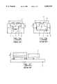
- FIG. 3is a diagrammatic perspective view of a hybrid optical element of the invention.
- FIG. 4is a diagrammatic longitudinal section view of the element shown in FIG. 3;
- FIG. 5is a diagrammatic cross-section view of a variant embodiment of a hybrid optical element of the invention.
- FIG. 3shows the structure of a hybrid optical element of the invention, and enables the manner in which it is assembled to be better understood.
- This hybrid optical elementincludes an active opto-electronic component 2, e.g. of the laser type or of the optical amplifier type, also referred to as a "chip", and a passive component 1 of the rectilinear light guide type or of the 3 dB coupler type, or of some other type.
- the passive component 1is made using a known method by stacking up successive layers 6, 7, and 8 of silica on a substrate 3 made of fused silica.
- the intermediate layer 7constitutes the core of the passive component, and it is etched into a special shape depending on the function of the light guide to be made.
- the other two layers 6 and 8constitute the cladding of the passive component.
- the fused silica substratemakes it possible to prevent stresses from forming in the layers 6, 7, 8 of silica, and thus enables a passive component to be obtained that is of good quality and that is insensitive to polarization.
- the assembly formed by the passive component 1 and by the silica substrate 3is referred to as the "silica-on-silica structure", and is referenced 100.
- the core 7 of the passive componentmay also be formed in a layer of silicon nitride (Si 3 N 4 ).
- a cavity 5is provided in the silica-on-silica structure 100, i.e. in or through the successive layers 6, 7, 8 of silica, and optionally into or through the substrate 3, to enable the opto-electronic component 2 to be received therein.
- the cavity 5may be chosen either to be a through cavity or to be a non-through cavity, the choice usually being made on the basis of manufacturing cost and of whether or not the active component 2 needs to be encapsulated.
- the opto-electronic component 2is inserted in the cavity 5 in a manner such that its optical axis 9 is in alignment with the light guide 7 of the passive component 1.
- the opto-electronic component 2may be a laser of the GaInAsP-on-InP type made in conventional manner by epitaxy and having power lying in the range 1 mW to 200 mW.
- the laser 2Prior to being inserted into the cavity 5, the laser 2 is fixed, e.g. by soldering, to an intermediate element 4 serving to dissipate the heat given off.
- the size of the intermediate elementis relatively small, its area is very slightly larger than that of the cavity 5, i.e. than that of the active component 2.
- the chip 2is inserted into the cavity 5 in a manner such that it is mounted "the right way up”. Conversely, it is placed “upside down" on the intermediate element 4, and it may be said to be a "flip chip" mounted thereon.
- abutments or keying meansare provided on the intermediate element 4, on the active component 2, and on the passive component 1.
- keying meansmay be formed by lithography, by Reactive Ion Etching (RIE), or by any other etching method.
- abutmentsare formed on the bottom surface of the heatsink 4 in a manner such that they can come into position against keying means 21 provided, for example, on the front surface 2b of the laser 2.
- abutments 41are provided on the bottom surface of the heatsink 4 in a manner such that they can come into position against markings, or in recesses 11 such as those shown in the example given in FIG. 3, provided in the top surface of the silica-on-silica structure 100.
- the intermediate element 4is positioned both relative to the laser 2 and relative to the passive component 1, the active component and the passive component are positioned relative to each other via a transitive relationship.
- the abutments on the heatsinkare positioned against the keying means 21 of the laser 2 very accurately, to within less than one micron.
- the abutments 41 on the heatsinkare provided such that they can be positioned against the markings 11 in the structure 100 with great accuracy, to within less than one micron.
- the markings 21 in the laser 2are aligned with its optical axis 9
- the keying means 11 on the passive component 1are aligned with the silica light guide 7, and the two types of abutment on the intermediate element 4 are aligned respectively with the keying means on the laser and with the keying means on the passive component.
- the locations of the abutments and keying meansare given merely by way of example. They may be placed otherwise, provided that they make it possible to fix the active component and the passive component relative to the heatsink 4, and thus relative to each other.
- the light guide 7 of the passive component 1is shown rectilinear, but it may be of more complex shape, and, in particular, it may, for example, be a 3 dB coupler.
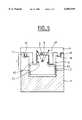
- FIG. 4is a diagrammatic longitudinal section view of the hybrid optical element shown in FIG. 3.
- the passive component 1is made up of a stack of layers of silica 6, 7, and 8. It includes a core 7, or light guide, etched to the desired dimensions and embedded in the cladding layers 6 and 8.
- the cavity 5 provided in the layers of silica of the passive component and in the substrate 3is a through cavity. This cavity 5 can receive the active opto-electronic component 2 in a manner such that the optical axis 9 thereof is aligned with the light guide 7 of the passive component 1.
- the chip 2is fixed by means of solder spots S1 to electrical connections 45 on the intermediate element 4 that acts as a heatsink.
- the heatsink 4is preferably made of silicon because silicon has a coefficient of thermal expansion similar to that of the GaInAsP/InP chip 2, so that it makes it possible to prevent shear stresses from being generated that could propagate in particular to the solder spots S1 between the chip 2 and the intermediate element 4.
- the intermediate element 4may be made of other materials such as alumina (Al 2 O 3 ) or gallium arsenide (GaAs), for example.
- Al 2 O 3does not enable abutments to be made with such great accuracy (to within less than one micron) so as to enable the optical axis of the active component to be aligned very accurately with the optical axis of the passive component.
- the substrate 3is made of fused silica. In a variant embodiment, it may optionally be made of quartz but quartz is more expensive than silica.
- abutments 42 provided on the bottom surface of the heatsink 4are designed to come into position snugly against the keying means 21 provided on the front face 2b of the laser 2.
- abutments 41are provided on the bottom surface of the heatsink 4 so as to be received against markings 11 provided in the top surface of the silica-on-silica structure 100.
- the silica-on-silica structure 100is further fixed to the heatsink 4 by solder spots S2 applied to the electrical connections 45 thereof.
- the abutments 41, 42 on the intermediate element 4, the keying means 21 on the laser 2 and the markings 11 in the passive component 1are, in the example shown in FIG. 4, aligned with the optical axis 9 of the laser and with the light guide 7 of the passive component.
- the silica-on-silica structure 100 used to make the hybrid optical device of the inventionhas large dimensions. Its area is greater than a few square millimeters, and it can be as much as a few tens of square centimeters.
- the "heat bridge" or heatsink 4 used in the present inventionhas an area that is small, and less than one square millimeter.
- This small areamakes it possible to limit the distance between the two solder spots S2 implemented between the silica-on-silica structure 100 and the heatsink 4, and, as a result, to limit in particular the risks of shear stresses occurring during standard telecommunications uses because of the difference between the coefficient of thermal expansion of silicon and the coefficient of thermal expansion of silica, such uses being made at temperatures that can vary in the range -40° C. to +85° C. This thus constitutes a major advantage over the prior art described above and corresponding to FIG. 2C.
- the chip 2is "flip chip" mounted on the intermediate element 4.
- the zone beneath the optical axis 9is doped with carriers of a first type, e.g. of the n type, while the zone situated above the optical axis 9 is doped with carriers of a second type, e.g. of the p type.
- the solder spots S1 serving to connect the chip to the heatsinkthus represent electrodes of a second type (positive electrodes in the example).
- the electrode of the first type(the negative electrode in the example) may be constituted by a conductor wire 15 soldered both to the connections 45 on the heatsink and to the zone of the laser 2 that is doped with n-type carriers.
- FIG. 5is a diagrammatic cross-section view of a variant embodiment of a hybrid optical device of the invention.
- the abutments 41 and 42 on the intermediate element 4are not aligned with the optical axes of the active component 2 and of the passive component 1, but rather they are provided in a direction that is perpendicular to said optical axes.
- Markings 11are provided in the top surface of the silica-on-silica structure 100 in a manner such that the abutments 41 on the heatsink 4 can be pressed therein, and the heatsink can be aligned relative to the passive component 1.
- the abutments 42 on the heatsink 4are provided such that they can be positioned against the side walls 22 of the front surface 2b of the laser 2.
- Solder spots S1one of which is visible in FIG. 5, make it possible to hold the laser 2 stationary on the heatsink 4.
- the solder spots making it possible to fix the silica-on-silica structure 100 to the heatsinkare not visible in this figure. Therefore, since the intermediate element 4 is fixed relative both to the passive component and to the active component, the two components are fixed and aligned relative to each other.
- the cavity 5is a non-through cavity. Therefore, in this case, the intermediate element 4, placed above the cavity, participates in encapsulating the active component.
- the arrows shownindicate the direction in which the heatgiven off by the laser 2 is removed.
- All of the above-described examplesrelate to a device including one active component and one passive component.
- a devicethat includes a plurality of other passive components, a plurality of other cavities, and a plurality of other intermediate elements, each of which is assembled to an active component and to the silica-on-silica structure so that each active component is situated inside a cavity and is coupled optically to a passive component.
Landscapes
- Physics & Mathematics (AREA)
- General Physics & Mathematics (AREA)
- Optics & Photonics (AREA)
- Optical Couplings Of Light Guides (AREA)
- Semiconductor Lasers (AREA)
- Optical Integrated Circuits (AREA)
Abstract
Description
Claims (9)
Applications Claiming Priority (2)
| Application Number | Priority Date | Filing Date | Title |
|---|---|---|---|
| FR9702165 | 1997-02-24 | ||
| FR9702165AFR2760101B1 (en) | 1997-02-24 | 1997-02-24 | METHOD FOR ASSEMBLING AN OPTO-HYBRID DEVICE |
Publications (1)
| Publication Number | Publication Date |
|---|---|
| US6093939Atrue US6093939A (en) | 2000-07-25 |
Family
ID=9504094
Family Applications (1)
| Application Number | Title | Priority Date | Filing Date |
|---|---|---|---|
| US09/028,816Expired - LifetimeUS6093939A (en) | 1997-02-24 | 1998-02-24 | Hybrid optical module including an intermediate element |
Country Status (5)
| Country | Link |
|---|---|
| US (1) | US6093939A (en) |
| EP (1) | EP0860724A1 (en) |
| JP (1) | JPH10274729A (en) |
| KR (1) | KR19980071602A (en) |
| FR (1) | FR2760101B1 (en) |
Cited By (26)
| Publication number | Priority date | Publication date | Assignee | Title |
|---|---|---|---|---|
| US6310364B1 (en)* | 1998-08-03 | 2001-10-30 | Toyoda Gosei Co., Ltd. | Light-emitting apparatus |
| US20020158190A1 (en)* | 2001-04-30 | 2002-10-31 | Jens Dieckroger | Configuration for detecting optical signals in at least one optical channel in a planar light circuit, attenuator including the configuration, and method for manufacturing the configuration |
| US6574382B2 (en)* | 1999-05-17 | 2003-06-03 | Chiaro Networks Ltd. | Modulated light source |
| WO2003034115A3 (en)* | 2001-10-17 | 2003-10-16 | Bookham Technology Plc | Coupling a semiconducter laser to an optical waveguide |
| US20030215194A1 (en)* | 2002-05-15 | 2003-11-20 | Kuhmann Jochen Friedrich | Optical device receiving substrate and optical device holding carrier |
| US6679635B2 (en) | 2000-09-27 | 2004-01-20 | Oki Electric Industry Co., Ltd. | Optical device permitting passive alignment of lens element |
| US20040012041A1 (en)* | 2002-07-22 | 2004-01-22 | Applied Materials, Inc. | Optical ready wafers |
| US20040013338A1 (en)* | 2002-07-22 | 2004-01-22 | Applied Materials, Inc. | Optical ready substrates |
| US20040114853A1 (en)* | 2002-07-22 | 2004-06-17 | Applied Materials, Inc. | Optical ready substrates |
| US20040219526A1 (en)* | 2003-04-07 | 2004-11-04 | Reddy M. Parameswara | Assay system using labeled oligonucleotides |
| US20050053383A1 (en)* | 2003-05-29 | 2005-03-10 | Applied Materials, Inc. | Serial routing of optical signals |
| FR2863716A1 (en)* | 2003-12-10 | 2005-06-17 | Commissariat Energie Atomique | Micro-opto-electro-mechanical system type optical micro-system, has optical structures with reference zones that are situated opposite to contact zones of mechanical structure, where reference zones are in stops on respective contact zones |
| US7103079B2 (en) | 2003-06-27 | 2006-09-05 | Applied Materials, Inc. | Pulsed quantum dot laser system with low jitter |
| US7101725B2 (en) | 2003-07-23 | 2006-09-05 | Applied Materials, Inc. | Solution to thermal budget |
| US20060222024A1 (en)* | 2005-03-15 | 2006-10-05 | Gray Allen L | Mode-locked semiconductor lasers with quantum-confined active region |
| US20060227825A1 (en)* | 2005-04-07 | 2006-10-12 | Nl-Nanosemiconductor Gmbh | Mode-locked quantum dot laser with controllable gain properties by multiple stacking |
| US20070053643A1 (en)* | 2005-09-01 | 2007-03-08 | Applied Materials, Inc. | Ridge technique for fabricating an optical detector and an optical waveguide |
| US20070104441A1 (en)* | 2005-11-08 | 2007-05-10 | Massachusetts Institute Of Technology | Laterally-integrated waveguide photodetector apparatus and related coupling methods |
| US20070127531A1 (en)* | 2005-12-07 | 2007-06-07 | Nl-Nanosemiconductor Gmbh | Laser source with broadband spectrum emission |
| US20080180674A1 (en)* | 2005-12-07 | 2008-07-31 | Innolume Gmbh | Optical Transmission System |
| US7555027B2 (en) | 2005-12-07 | 2009-06-30 | Innolume Gmbh | Laser source with broadband spectrum emission |
| US20100142973A1 (en)* | 2005-12-07 | 2010-06-10 | Innolume Gmbh | Semiconductor laser with low relative intensity noise of individual longitudinal modes and optical transmission system incorporating the laser |
| US20100303110A1 (en)* | 2009-05-26 | 2010-12-02 | Venkata Adiseshaiah Bhagavatula | Edge Bonded Optical Packages |
| US20100303109A1 (en)* | 2009-05-26 | 2010-12-02 | Venkata Adiseshaiah Bhagavatula | Proximity Coupled Athermal Optical Package Comprising Laser Source And Compound Facet Wavelength Conversion Device |
| US20110205619A1 (en)* | 2010-02-22 | 2011-08-25 | Douglas Llewellyn Butler | Wavelength Conversion Device With Microlens And Optical Package Incorporating The Same |
| WO2014087346A1 (en)* | 2012-12-07 | 2014-06-12 | Telefonaktiebolaget L M Ericsson (Publ) | Method and apparatus for coupling to an optical waveguide in a silicon photonics die |
Families Citing this family (1)
| Publication number | Priority date | Publication date | Assignee | Title |
|---|---|---|---|---|
| JP7056436B2 (en)* | 2018-07-24 | 2022-04-19 | 住友電気工業株式会社 | Manufacturing method of optical semiconductor device, susceptor and its manufacturing method |
Citations (3)
| Publication number | Priority date | Publication date | Assignee | Title |
|---|---|---|---|---|
| EP0118185A1 (en)* | 1983-02-04 | 1984-09-12 | Sumitomo Electric Industries Limited | Integrated optical circuit device |
| WO1993025924A1 (en)* | 1992-06-15 | 1993-12-23 | Robert Bosch Gmbh | Optical polymer element for coupling photoelements to integrated optical circuits |
| DE4401219A1 (en)* | 1994-01-18 | 1995-07-20 | Bosch Gmbh Robert | Integrated optical component and method for producing an integrated optical component |
Family Cites Families (1)
| Publication number | Priority date | Publication date | Assignee | Title |
|---|---|---|---|---|
| ATE50864T1 (en)* | 1985-10-16 | 1990-03-15 | British Telecomm | FABRY-PEROT INTERFEROMETER. |
- 1997
- 1997-02-24FRFR9702165Apatent/FR2760101B1/ennot_activeExpired - Fee Related
- 1998
- 1998-02-16EPEP98400352Apatent/EP0860724A1/ennot_activeWithdrawn
- 1998-02-23KRKR1019980005568Apatent/KR19980071602A/ennot_activeWithdrawn
- 1998-02-24JPJP10042362Apatent/JPH10274729A/enactivePending
- 1998-02-24USUS09/028,816patent/US6093939A/ennot_activeExpired - Lifetime
Patent Citations (3)
| Publication number | Priority date | Publication date | Assignee | Title |
|---|---|---|---|---|
| EP0118185A1 (en)* | 1983-02-04 | 1984-09-12 | Sumitomo Electric Industries Limited | Integrated optical circuit device |
| WO1993025924A1 (en)* | 1992-06-15 | 1993-12-23 | Robert Bosch Gmbh | Optical polymer element for coupling photoelements to integrated optical circuits |
| DE4401219A1 (en)* | 1994-01-18 | 1995-07-20 | Bosch Gmbh Robert | Integrated optical component and method for producing an integrated optical component |
Non-Patent Citations (4)
| Title |
|---|
| D. Peters et al, "Integrated Optical Devices with Silicon Oxynitride Prepared by PECVD on Si and GaAs Substrates", SPIE, Physical Concepts of Materials for Novel Optoelectronics Device Applications II: Device Physics and Applications, vol. 1362, Oct. 28, 1990-Nov. 2, 1990, AACHEN, pp. 338-349. |
| D. Peters et al, Integrated Optical Devices with Silicon Oxynitride Prepared by PECVD on Si and GaAs Substrates , SPIE, Physical Concepts of Materials for Novel Optoelectronics Device Applications II: Device Physics and Applications, vol. 1362, Oct. 28, 1990 Nov. 2, 1990, AACHEN, pp. 338 349.* |
| I. Kitazawa et al, "Thermal Resistance and Soldering Stress Analyses on LD-Mount-Structures for Planar Lightwave Circuits", IOOC '95, 1995, pp. 28-29. |
| I. Kitazawa et al, Thermal Resistance and Soldering Stress Analyses on LD Mount Structures for Planar Lightwave Circuits , IOOC 95, 1995, pp. 28 29.* |
Cited By (46)
| Publication number | Priority date | Publication date | Assignee | Title |
|---|---|---|---|---|
| US6310364B1 (en)* | 1998-08-03 | 2001-10-30 | Toyoda Gosei Co., Ltd. | Light-emitting apparatus |
| US6878971B2 (en) | 1998-08-03 | 2005-04-12 | Toyoda Gosei Co., Ltd. | Light-emitting apparatus |
| US6574382B2 (en)* | 1999-05-17 | 2003-06-03 | Chiaro Networks Ltd. | Modulated light source |
| US6917725B2 (en)* | 1999-05-17 | 2005-07-12 | Chiaro Networks Ltd. | Modulated light source |
| US20040017963A1 (en)* | 1999-05-17 | 2004-01-29 | Chiaro Networks Ltd. | Modulated light source |
| US6679635B2 (en) | 2000-09-27 | 2004-01-20 | Oki Electric Industry Co., Ltd. | Optical device permitting passive alignment of lens element |
| US20020158190A1 (en)* | 2001-04-30 | 2002-10-31 | Jens Dieckroger | Configuration for detecting optical signals in at least one optical channel in a planar light circuit, attenuator including the configuration, and method for manufacturing the configuration |
| WO2002088812A1 (en)* | 2001-04-30 | 2002-11-07 | Infineon Technologies Ag | Arrangement for detecting optical signals of a planar optical circuit |
| US6894269B2 (en) | 2001-04-30 | 2005-05-17 | Optun (Bvi) Ltd. | Configuration for detecting optical signals in at least one optical channel in a planar light circuit, attenuator including the configuration, and method for manufacturing the configuration |
| WO2003034115A3 (en)* | 2001-10-17 | 2003-10-16 | Bookham Technology Plc | Coupling a semiconducter laser to an optical waveguide |
| US20030215194A1 (en)* | 2002-05-15 | 2003-11-20 | Kuhmann Jochen Friedrich | Optical device receiving substrate and optical device holding carrier |
| WO2003098302A3 (en)* | 2002-05-15 | 2004-02-19 | Hymite As | Optical device receiving substrate and optical device holding carrier |
| US7213978B2 (en) | 2002-05-15 | 2007-05-08 | Hymite A/S | Optical device receiving substrate and optical device holding carrier |
| US20040114853A1 (en)* | 2002-07-22 | 2004-06-17 | Applied Materials, Inc. | Optical ready substrates |
| US20040013338A1 (en)* | 2002-07-22 | 2004-01-22 | Applied Materials, Inc. | Optical ready substrates |
| US20040012041A1 (en)* | 2002-07-22 | 2004-01-22 | Applied Materials, Inc. | Optical ready wafers |
| US20070080414A1 (en)* | 2002-07-22 | 2007-04-12 | Applied Materials, Inc. | Optical ready substrates |
| US7110629B2 (en) | 2002-07-22 | 2006-09-19 | Applied Materials, Inc. | Optical ready substrates |
| US7043106B2 (en) | 2002-07-22 | 2006-05-09 | Applied Materials, Inc. | Optical ready wafers |
| US7072534B2 (en) | 2002-07-22 | 2006-07-04 | Applied Materials, Inc. | Optical ready substrates |
| US20040219526A1 (en)* | 2003-04-07 | 2004-11-04 | Reddy M. Parameswara | Assay system using labeled oligonucleotides |
| US7529435B2 (en) | 2003-05-29 | 2009-05-05 | Applied Materials, Inc. | Serial routing of optical signals |
| US20050053383A1 (en)* | 2003-05-29 | 2005-03-10 | Applied Materials, Inc. | Serial routing of optical signals |
| US7103079B2 (en) | 2003-06-27 | 2006-09-05 | Applied Materials, Inc. | Pulsed quantum dot laser system with low jitter |
| US7101725B2 (en) | 2003-07-23 | 2006-09-05 | Applied Materials, Inc. | Solution to thermal budget |
| WO2005059613A1 (en)* | 2003-12-10 | 2005-06-30 | Commissariat A L'energie Atomique | Optical microsystem comprising mechanical stops for the positioning of optical structures |
| FR2863716A1 (en)* | 2003-12-10 | 2005-06-17 | Commissariat Energie Atomique | Micro-opto-electro-mechanical system type optical micro-system, has optical structures with reference zones that are situated opposite to contact zones of mechanical structure, where reference zones are in stops on respective contact zones |
| US20060222024A1 (en)* | 2005-03-15 | 2006-10-05 | Gray Allen L | Mode-locked semiconductor lasers with quantum-confined active region |
| US20060227825A1 (en)* | 2005-04-07 | 2006-10-12 | Nl-Nanosemiconductor Gmbh | Mode-locked quantum dot laser with controllable gain properties by multiple stacking |
| US20070053643A1 (en)* | 2005-09-01 | 2007-03-08 | Applied Materials, Inc. | Ridge technique for fabricating an optical detector and an optical waveguide |
| US7760980B2 (en) | 2005-09-01 | 2010-07-20 | Applied Materials, Inc. | Ridge technique for fabricating an optical detector and an optical waveguide |
| US20070104441A1 (en)* | 2005-11-08 | 2007-05-10 | Massachusetts Institute Of Technology | Laterally-integrated waveguide photodetector apparatus and related coupling methods |
| WO2007055739A1 (en)* | 2005-11-08 | 2007-05-18 | Massachusetts Institute Of Technology | Laterally-integrated waveguide photodetector apparatus and related coupling methods |
| US7555027B2 (en) | 2005-12-07 | 2009-06-30 | Innolume Gmbh | Laser source with broadband spectrum emission |
| US20080180674A1 (en)* | 2005-12-07 | 2008-07-31 | Innolume Gmbh | Optical Transmission System |
| US7561607B2 (en) | 2005-12-07 | 2009-07-14 | Innolume Gmbh | Laser source with broadband spectrum emission |
| US20100142973A1 (en)* | 2005-12-07 | 2010-06-10 | Innolume Gmbh | Semiconductor laser with low relative intensity noise of individual longitudinal modes and optical transmission system incorporating the laser |
| US20070127531A1 (en)* | 2005-12-07 | 2007-06-07 | Nl-Nanosemiconductor Gmbh | Laser source with broadband spectrum emission |
| US7835408B2 (en) | 2005-12-07 | 2010-11-16 | Innolume Gmbh | Optical transmission system |
| US8411711B2 (en) | 2005-12-07 | 2013-04-02 | Innolume Gmbh | Semiconductor laser with low relative intensity noise of individual longitudinal modes and optical transmission system incorporating the laser |
| US20100303110A1 (en)* | 2009-05-26 | 2010-12-02 | Venkata Adiseshaiah Bhagavatula | Edge Bonded Optical Packages |
| US20100303109A1 (en)* | 2009-05-26 | 2010-12-02 | Venkata Adiseshaiah Bhagavatula | Proximity Coupled Athermal Optical Package Comprising Laser Source And Compound Facet Wavelength Conversion Device |
| US8102887B2 (en) | 2009-05-26 | 2012-01-24 | Corning Incorporated | Edge bonded optical packages |
| US20110205619A1 (en)* | 2010-02-22 | 2011-08-25 | Douglas Llewellyn Butler | Wavelength Conversion Device With Microlens And Optical Package Incorporating The Same |
| US8111452B2 (en) | 2010-02-22 | 2012-02-07 | Corning Incorporated | Wavelength conversion device with microlens and optical package incorporating the same |
| WO2014087346A1 (en)* | 2012-12-07 | 2014-06-12 | Telefonaktiebolaget L M Ericsson (Publ) | Method and apparatus for coupling to an optical waveguide in a silicon photonics die |
Also Published As
| Publication number | Publication date |
|---|---|
| FR2760101A1 (en) | 1998-08-28 |
| FR2760101B1 (en) | 1999-04-16 |
| EP0860724A1 (en) | 1998-08-26 |
| KR19980071602A (en) | 1998-10-26 |
| JPH10274729A (en) | 1998-10-13 |
Similar Documents
| Publication | Publication Date | Title |
|---|---|---|
| US6093939A (en) | Hybrid optical module including an intermediate element | |
| US10761279B2 (en) | Method of producing a device for adiabatic coupling between waveguide arrays, corresponding device, and system | |
| US11531171B2 (en) | Photonic chip with integrated collimation structure | |
| US10222565B2 (en) | Optically aligned hybrid semiconductor device and method | |
| US5319725A (en) | Bilithic composite for optoelectronic integration | |
| US5247597A (en) | Optical fiber alignment | |
| KR100277695B1 (en) | Method for manufacturing a substrate for hybrid optical integrated circuit using S-O optical waveguide | |
| US5703980A (en) | Method for low-loss insertion of an optical signal from an optical fibre to a waveguide integrated on to a semiconductor wafer | |
| US12379555B2 (en) | Detachable connector for co-packaged optics | |
| US10802215B2 (en) | Optical waveguide, corresponding coupling arrangement, apparatus and method | |
| US7447400B2 (en) | Optical waveguide substrate and method of fabricating the same | |
| JPH09311253A (en) | Optical coupling structure and manufacturing method thereof | |
| US20170108643A1 (en) | Optical component with angled-facet waveguide | |
| US20070278666A1 (en) | Method for Production of Electronic and Optoelectronic Circuits | |
| US20010028768A1 (en) | Optical waveguide transmitter-receiver module | |
| US11934007B2 (en) | Assembly of an active semiconductor component and of a silicon-based passive optical component | |
| US20230141467A1 (en) | Hybrid integration method | |
| Mino et al. | Planar lightwave circuit platform with coplanar waveguide for opto-electronic hybrid integration | |
| JPS62106686A (en) | semiconductor laser equipment | |
| JPH11271572A (en) | Optical coupling system, optical module, and optical transmission system | |
| JP2608585B2 (en) | Hybrid optical integrated circuit | |
| US20250155644A1 (en) | Optical connection structure, optical module, and method for manufacturing optical module | |
| Armiento | Hybrid optoelectronic integration of transmitter arrays on silicon waferboard | |
| Kurata et al. | 9 Passive Alignment for Surface Mount Packaging and as an Application of the Passive Optical Alignment Method | |
| Hunziker et al. | 4 Silicon Waferboard Mechanical Passive Alignment II |
Legal Events
| Date | Code | Title | Description |
|---|---|---|---|
| AS | Assignment | Owner name:ALCATEL ALSTHOM COMPAGNIE GENERALE D'ELECTRICITE, Free format text:ASSIGNMENT OF ASSIGNORS INTEREST;ASSIGNORS:ARTIGUE, CLAUDE;TREGOAT, DENIS;MALLECOT, FRANCK;AND OTHERS;REEL/FRAME:009262/0585 Effective date:19980202 | |
| AS | Assignment | Owner name:ALCATEL, FRANCE Free format text:CHANGE OF NAME;ASSIGNOR:ALCATEL ALSTHOM COMPAGNIE GENERALE D'ELECTRICITE;REEL/FRAME:010084/0223 Effective date:19980914 | |
| FEPP | Fee payment procedure | Free format text:PAYOR NUMBER ASSIGNED (ORIGINAL EVENT CODE: ASPN); ENTITY STATUS OF PATENT OWNER: LARGE ENTITY | |
| STCF | Information on status: patent grant | Free format text:PATENTED CASE | |
| AS | Assignment | Owner name:AVANEX CORPORATION, CALIFORNIA Free format text:ASSIGNMENT OF ASSIGNORS INTEREST;ASSIGNOR:ALCATEL;REEL/FRAME:014066/0747 Effective date:20030731 | |
| FPAY | Fee payment | Year of fee payment:4 | |
| AS | Assignment | Owner name:HBK INVESTMENTS L.P., TEXAS Free format text:SECURITY AGREEMENT;ASSIGNOR:AVANEX CORPORATION;REEL/FRAME:016079/0174 Effective date:20050519 | |
| AS | Assignment | Owner name:AVANEX CORPORATION, CALIFORNIA Free format text:RELEASE BY SECURED PARTY;ASSIGNOR:HBK INVESTMENTS, L.P.;REEL/FRAME:019035/0342 Effective date:20070312 | |
| FPAY | Fee payment | Year of fee payment:8 | |
| FPAY | Fee payment | Year of fee payment:12 | |
| AS | Assignment | Owner name:WELLS FARGO CAPITAL FINANCE, INC., AS AGENT, CALIF Free format text:PATENT SECURITY AGREEMENT;ASSIGNOR:OCLARO (NORTH AMERICA), INC.;REEL/FRAME:028435/0773 Effective date:20110726 | |
| AS | Assignment | Owner name:SILICON VALLEY BANK, CALIFORNIA Free format text:SECURITY INTEREST;ASSIGNORS:OCLARO, INC.;OCLARO TECHNOLOGY, INC.;OCLARO (NORTH AMERICA), INC.;AND OTHERS;REEL/FRAME:032589/0948 Effective date:20140328 | |
| AS | Assignment | Owner name:OCLARO (NORTH AMERICA), INC., CALIFORNIA Free format text:RELEASE BY SECURED PARTY;ASSIGNOR:WELLS FARGO CAPITAL FINANCE, LLC;REEL/FRAME:032643/0427 Effective date:20140325 | |
| AS | Assignment | Owner name:OCLARO (NORTH AMERICA), INC., CALIFORNIA Free format text:CHANGE OF NAME;ASSIGNOR:AVANEX CORPORATION;REEL/FRAME:032826/0276 Effective date:20090707 | |
| AS | Assignment | Owner name:OCLARO TECHNOLOGY, INC., CALIFORNIA Free format text:RELEASE BY SECURED PARTY;ASSIGNOR:SILICON VALLEY BANK;REEL/FRAME:042430/0235 Effective date:20170331 Owner name:OPNEXT SUBSYSTEMS INC., CALIFORNIA Free format text:RELEASE BY SECURED PARTY;ASSIGNOR:SILICON VALLEY BANK;REEL/FRAME:042430/0235 Effective date:20170331 Owner name:OCLARO TECHNOLOGY LIMITED, CALIFORNIA Free format text:RELEASE BY SECURED PARTY;ASSIGNOR:SILICON VALLEY BANK;REEL/FRAME:042430/0235 Effective date:20170331 Owner name:OCLARO, INC., CALIFORNIA Free format text:RELEASE BY SECURED PARTY;ASSIGNOR:SILICON VALLEY BANK;REEL/FRAME:042430/0235 Effective date:20170331 Owner name:BOOKHAM NOMINEES LIMITED, CALIFORNIA Free format text:RELEASE BY SECURED PARTY;ASSIGNOR:SILICON VALLEY BANK;REEL/FRAME:042430/0235 Effective date:20170331 Owner name:OPNEXT, INC., CALIFORNIA Free format text:RELEASE BY SECURED PARTY;ASSIGNOR:SILICON VALLEY BANK;REEL/FRAME:042430/0235 Effective date:20170331 Owner name:OCLARO INNOVATIONS LLP, CALIFORNIA Free format text:RELEASE BY SECURED PARTY;ASSIGNOR:SILICON VALLEY BANK;REEL/FRAME:042430/0235 Effective date:20170331 Owner name:PINE PHOTONICS COMMUNICATIONS, INC., CALIFORNIA Free format text:RELEASE BY SECURED PARTY;ASSIGNOR:SILICON VALLEY BANK;REEL/FRAME:042430/0235 Effective date:20170331 Owner name:MINTERA CORPORATION, CALIFORNIA Free format text:RELEASE BY SECURED PARTY;ASSIGNOR:SILICON VALLEY BANK;REEL/FRAME:042430/0235 Effective date:20170331 Owner name:OCLARO (NORTH AMERICA), INC., CALIFORNIA Free format text:RELEASE BY SECURED PARTY;ASSIGNOR:SILICON VALLEY BANK;REEL/FRAME:042430/0235 Effective date:20170331 |