US6093035A - Contact for use in an electrical connector - Google Patents
Contact for use in an electrical connectorDownload PDFInfo
- Publication number
- US6093035A US6093035AUS08/778,398US77839896AUS6093035AUS 6093035 AUS6093035 AUS 6093035AUS 77839896 AUS77839896 AUS 77839896AUS 6093035 AUS6093035 AUS 6093035A
- Authority
- US
- United States
- Prior art keywords
- contact
- solder
- recited
- contacts
- recess
- Prior art date
- Legal status (The legal status is an assumption and is not a legal conclusion. Google has not performed a legal analysis and makes no representation as to the accuracy of the status listed.)
- Expired - Lifetime
Links
- 229910000679solderInorganic materials0.000claimsabstractdescription215
- 239000000758substrateSubstances0.000claimsabstractdescription27
- PXHVJJICTQNCMI-UHFFFAOYSA-NNickelChemical compound[Ni]PXHVJJICTQNCMI-UHFFFAOYSA-N0.000claimsdescription33
- 239000000463materialSubstances0.000claimsdescription32
- 229910052759nickelInorganic materials0.000claimsdescription17
- PCHJSUWPFVWCPO-UHFFFAOYSA-NgoldChemical compound[Au]PCHJSUWPFVWCPO-UHFFFAOYSA-N0.000claimsdescription14
- 229910052737goldInorganic materials0.000claimsdescription14
- 239000010931goldSubstances0.000claimsdescription14
- 230000013011matingEffects0.000claimsdescription12
- 238000007747platingMethods0.000claimsdescription11
- KDLHZDBZIXYQEI-UHFFFAOYSA-NPalladiumChemical compound[Pd]KDLHZDBZIXYQEI-UHFFFAOYSA-N0.000claimsdescription6
- 229910052751metalInorganic materials0.000claimsdescription6
- 239000002184metalSubstances0.000claimsdescription6
- 229910052718tinInorganic materials0.000claimsdescription6
- 238000000576coating methodMethods0.000claimsdescription5
- 229910001252Pd alloyInorganic materials0.000claimsdescription3
- ATJFFYVFTNAWJD-UHFFFAOYSA-NTinChemical compound[Sn]ATJFFYVFTNAWJD-UHFFFAOYSA-N0.000claimsdescription3
- 239000011248coating agentSubstances0.000claimsdescription3
- 229910052763palladiumInorganic materials0.000claimsdescription3
- 229910001128Sn alloyInorganic materials0.000claimsdescription2
- 238000000034methodMethods0.000abstractdescription31
- 230000008569processEffects0.000abstractdescription5
- 238000004519manufacturing processMethods0.000abstractdescription3
- 230000004907fluxEffects0.000description9
- 238000002844meltingMethods0.000description8
- 230000008018meltingEffects0.000description8
- 230000002093peripheral effectEffects0.000description8
- 239000006071creamSubstances0.000description7
- 229910045601alloyInorganic materials0.000description6
- 239000000956alloySubstances0.000description6
- 230000006870functionEffects0.000description6
- 238000003780insertionMethods0.000description6
- 230000037431insertionEffects0.000description6
- 230000014759maintenance of locationEffects0.000description6
- 229920000106Liquid crystal polymerPolymers0.000description5
- 239000004977Liquid-crystal polymers (LCPs)Substances0.000description5
- 238000010438heat treatmentMethods0.000description5
- 238000005476solderingMethods0.000description5
- RSWGJHLUYNHPMX-UHFFFAOYSA-NAbietic-SaeureNatural productsC12CCC(C(C)C)=CC2=CCC2C1(C)CCCC2(C)C(O)=ORSWGJHLUYNHPMX-UHFFFAOYSA-N0.000description4
- KHPCPRHQVVSZAH-HUOMCSJISA-NRosinNatural productsO(C/C=C/c1ccccc1)[C@H]1[C@H](O)[C@@H](O)[C@@H](O)[C@@H](CO)O1KHPCPRHQVVSZAH-HUOMCSJISA-N0.000description4
- 238000005452bendingMethods0.000description4
- KHPCPRHQVVSZAH-UHFFFAOYSA-Ntrans-cinnamyl beta-D-glucopyranosideNatural productsOC1C(O)C(O)C(CO)OC1OCC=CC1=CC=CC=C1KHPCPRHQVVSZAH-UHFFFAOYSA-N0.000description4
- 230000006835compressionEffects0.000description3
- 238000007906compressionMethods0.000description3
- 239000004020conductorSubstances0.000description3
- 230000001965increasing effectEffects0.000description3
- 239000007788liquidSubstances0.000description3
- 238000002161passivationMethods0.000description3
- 239000000843powderSubstances0.000description3
- 239000010970precious metalSubstances0.000description3
- 230000000717retained effectEffects0.000description3
- 238000011179visual inspectionMethods0.000description3
- NBIIXXVUZAFLBC-UHFFFAOYSA-NPhosphoric acidChemical compoundOP(O)(O)=ONBIIXXVUZAFLBC-UHFFFAOYSA-N0.000description2
- 239000000919ceramicSubstances0.000description2
- 239000003795chemical substances by applicationSubstances0.000description2
- 238000010276constructionMethods0.000description2
- 230000000694effectsEffects0.000description2
- 230000005496eutecticsEffects0.000description2
- 239000012634fragmentSubstances0.000description2
- 229910052745leadInorganic materials0.000description2
- 239000007791liquid phaseSubstances0.000description2
- 150000007522mineralic acidsChemical class0.000description2
- 239000000203mixtureSubstances0.000description2
- 238000000465mouldingMethods0.000description2
- 229910000480nickel oxideInorganic materials0.000description2
- 150000007524organic acidsChemical class0.000description2
- GNRSAWUEBMWBQH-UHFFFAOYSA-NoxonickelChemical compound[Ni]=OGNRSAWUEBMWBQH-UHFFFAOYSA-N0.000description2
- 238000009736wettingMethods0.000description2
- 229910001316Ag alloyInorganic materials0.000description1
- 235000001674Agaricus brunnescensNutrition0.000description1
- VYZAMTAEIAYCRO-UHFFFAOYSA-NChromiumChemical compound[Cr]VYZAMTAEIAYCRO-UHFFFAOYSA-N0.000description1
- 239000004593EpoxySubstances0.000description1
- KRHYYFGTRYWZRS-UHFFFAOYSA-MFluoride anionChemical compound[F-]KRHYYFGTRYWZRS-UHFFFAOYSA-M0.000description1
- QCEUXSAXTBNJGO-UHFFFAOYSA-N[Ag].[Sn]Chemical compound[Ag].[Sn]QCEUXSAXTBNJGO-UHFFFAOYSA-N0.000description1
- 238000010521absorption reactionMethods0.000description1
- 230000035508accumulationEffects0.000description1
- 238000009825accumulationMethods0.000description1
- 239000002253acidSubstances0.000description1
- 150000007513acidsChemical class0.000description1
- 238000007792additionMethods0.000description1
- 239000012080ambient airSubstances0.000description1
- GVFOJDIFWSDNOY-UHFFFAOYSA-Nantimony tinChemical compound[Sn].[Sb]GVFOJDIFWSDNOY-UHFFFAOYSA-N0.000description1
- 125000003118aryl groupChemical group0.000description1
- 230000004888barrier functionEffects0.000description1
- 230000008901benefitEffects0.000description1
- DMFGNRRURHSENX-UHFFFAOYSA-Nberyllium copperChemical compound[Be].[Cu]DMFGNRRURHSENX-UHFFFAOYSA-N0.000description1
- 230000015572biosynthetic processEffects0.000description1
- 230000001680brushing effectEffects0.000description1
- 230000008859changeEffects0.000description1
- 229910052804chromiumInorganic materials0.000description1
- 239000011651chromiumSubstances0.000description1
- 239000000470constituentSubstances0.000description1
- 238000001816coolingMethods0.000description1
- 230000003247decreasing effectEffects0.000description1
- 230000001419dependent effectEffects0.000description1
- 238000011161developmentMethods0.000description1
- 230000018109developmental processEffects0.000description1
- 238000006073displacement reactionMethods0.000description1
- 238000005516engineering processMethods0.000description1
- -1for exampleSubstances0.000description1
- 230000009477glass transitionEffects0.000description1
- 229910052738indiumInorganic materials0.000description1
- APFVFJFRJDLVQX-UHFFFAOYSA-Nindium atomChemical compound[In]APFVFJFRJDLVQX-UHFFFAOYSA-N0.000description1
- 230000001939inductive effectEffects0.000description1
- LWUVWAREOOAHDW-UHFFFAOYSA-Nlead silverChemical compound[Ag].[Pb]LWUVWAREOOAHDW-UHFFFAOYSA-N0.000description1
- 239000004973liquid crystal related substanceSubstances0.000description1
- 150000002739metalsChemical class0.000description1
- 230000004048modificationEffects0.000description1
- 238000012986modificationMethods0.000description1
- 150000002815nickelChemical class0.000description1
- ZQPPMHVWECSIRJ-KTKRTIGZSA-Noleic acid groupChemical groupC(CCCCCCC\C=C/CCCCCCCC)(=O)OZQPPMHVWECSIRJ-KTKRTIGZSA-N0.000description1
- 235000005985organic acidsNutrition0.000description1
- 230000003647oxidationEffects0.000description1
- 238000007254oxidation reactionMethods0.000description1
- 230000001590oxidative effectEffects0.000description1
- 239000012071phaseSubstances0.000description1
- 235000011007phosphoric acidNutrition0.000description1
- 239000004033plasticSubstances0.000description1
- 229920000728polyesterPolymers0.000description1
- 230000008439repair processEffects0.000description1
- 230000033458reproductionEffects0.000description1
- 238000012216screeningMethods0.000description1
- 229920001169thermoplasticPolymers0.000description1
- 239000004416thermosoftening plasticSubstances0.000description1
Images


Classifications
- H—ELECTRICITY
- H01—ELECTRIC ELEMENTS
- H01R—ELECTRICALLY-CONDUCTIVE CONNECTIONS; STRUCTURAL ASSOCIATIONS OF A PLURALITY OF MUTUALLY-INSULATED ELECTRICAL CONNECTING ELEMENTS; COUPLING DEVICES; CURRENT COLLECTORS
- H01R43/00—Apparatus or processes specially adapted for manufacturing, assembling, maintaining, or repairing of line connectors or current collectors or for joining electric conductors
- H01R43/02—Apparatus or processes specially adapted for manufacturing, assembling, maintaining, or repairing of line connectors or current collectors or for joining electric conductors for soldered or welded connections
- H01R43/0256—Apparatus or processes specially adapted for manufacturing, assembling, maintaining, or repairing of line connectors or current collectors or for joining electric conductors for soldered or welded connections for soldering or welding connectors to a printed circuit board
- H—ELECTRICITY
- H01—ELECTRIC ELEMENTS
- H01R—ELECTRICALLY-CONDUCTIVE CONNECTIONS; STRUCTURAL ASSOCIATIONS OF A PLURALITY OF MUTUALLY-INSULATED ELECTRICAL CONNECTING ELEMENTS; COUPLING DEVICES; CURRENT COLLECTORS
- H01R12/00—Structural associations of a plurality of mutually-insulated electrical connecting elements, specially adapted for printed circuits, e.g. printed circuit boards [PCB], flat or ribbon cables, or like generally planar structures, e.g. terminal strips, terminal blocks; Coupling devices specially adapted for printed circuits, flat or ribbon cables, or like generally planar structures; Terminals specially adapted for contact with, or insertion into, printed circuits, flat or ribbon cables, or like generally planar structures
- H01R12/70—Coupling devices
- H01R12/71—Coupling devices for rigid printing circuits or like structures
- H01R12/712—Coupling devices for rigid printing circuits or like structures co-operating with the surface of the printed circuit or with a coupling device exclusively provided on the surface of the printed circuit
- H01R12/716—Coupling device provided on the PCB
- H—ELECTRICITY
- H01—ELECTRIC ELEMENTS
- H01R—ELECTRICALLY-CONDUCTIVE CONNECTIONS; STRUCTURAL ASSOCIATIONS OF A PLURALITY OF MUTUALLY-INSULATED ELECTRICAL CONNECTING ELEMENTS; COUPLING DEVICES; CURRENT COLLECTORS
- H01R43/00—Apparatus or processes specially adapted for manufacturing, assembling, maintaining, or repairing of line connectors or current collectors or for joining electric conductors
- H01R43/20—Apparatus or processes specially adapted for manufacturing, assembling, maintaining, or repairing of line connectors or current collectors or for joining electric conductors for assembling or disassembling contact members with insulating base, case or sleeve
- H—ELECTRICITY
- H05—ELECTRIC TECHNIQUES NOT OTHERWISE PROVIDED FOR
- H05K—PRINTED CIRCUITS; CASINGS OR CONSTRUCTIONAL DETAILS OF ELECTRIC APPARATUS; MANUFACTURE OF ASSEMBLAGES OF ELECTRICAL COMPONENTS
- H05K3/00—Apparatus or processes for manufacturing printed circuits
- H05K3/30—Assembling printed circuits with electric components, e.g. with resistor
- H05K3/32—Assembling printed circuits with electric components, e.g. with resistor electrically connecting electric components or wires to printed circuits
- H05K3/34—Assembling printed circuits with electric components, e.g. with resistor electrically connecting electric components or wires to printed circuits by soldering
- H05K3/341—Surface mounted components
- H05K3/3421—Leaded components
- H05K3/3426—Leaded components characterised by the leads
- H—ELECTRICITY
- H05—ELECTRIC TECHNIQUES NOT OTHERWISE PROVIDED FOR
- H05K—PRINTED CIRCUITS; CASINGS OR CONSTRUCTIONAL DETAILS OF ELECTRIC APPARATUS; MANUFACTURE OF ASSEMBLAGES OF ELECTRICAL COMPONENTS
- H05K3/00—Apparatus or processes for manufacturing printed circuits
- H05K3/30—Assembling printed circuits with electric components, e.g. with resistor
- H05K3/32—Assembling printed circuits with electric components, e.g. with resistor electrically connecting electric components or wires to printed circuits
- H05K3/34—Assembling printed circuits with electric components, e.g. with resistor electrically connecting electric components or wires to printed circuits by soldering
- H05K3/3457—Solder materials or compositions; Methods of application thereof
- H05K3/3478—Applying solder preforms; Transferring prefabricated solder patterns
- Y—GENERAL TAGGING OF NEW TECHNOLOGICAL DEVELOPMENTS; GENERAL TAGGING OF CROSS-SECTIONAL TECHNOLOGIES SPANNING OVER SEVERAL SECTIONS OF THE IPC; TECHNICAL SUBJECTS COVERED BY FORMER USPC CROSS-REFERENCE ART COLLECTIONS [XRACs] AND DIGESTS
- Y02—TECHNOLOGIES OR APPLICATIONS FOR MITIGATION OR ADAPTATION AGAINST CLIMATE CHANGE
- Y02E—REDUCTION OF GREENHOUSE GAS [GHG] EMISSIONS, RELATED TO ENERGY GENERATION, TRANSMISSION OR DISTRIBUTION
- Y02E60/00—Enabling technologies; Technologies with a potential or indirect contribution to GHG emissions mitigation
- Y02E60/10—Energy storage using batteries
Definitions
- the present inventionrelates to electrical connectors and more particularly high I/O density connectors, such as array connectors.
- Efforts to miniaturize connectorshave included reducing the pitch between terminals in single or double row linear connectors, so that a relatively high number of I/O or other lines can be interconnected by connectors that fit within tightly circumscribed areas on the circuit substrates allotted for receiving connectors.
- the drive for miniaturizationhas also been accompanied by a shift in preference to surface mount techniques (SMT) for mounting components on circuit boards.
- SMTsurface mount techniques
- solder balls attached to the IC packageare positioned on electrical contact pads of a circuit substrate to which a layer of solder paste has been applied, typically by use of a screen or mask.
- the unitis then heated to a temperature at which the solder paste and at least a portion or all of the solder ball melt and fuse to an underlying conductive pad formed on the circuit substrate.
- the ICis thereby connected to the substrate without need of external leads on the IC.
- Coplanarity of the solder ballsis influenced by the size of the solder ball and its positioning on the connector.
- the final size of the ballis dependent on the total volume of solder initially available in both the solder paste and the solder balls.
- this considerationpresents particular challenges because variations in the volume of the connector contact received within the solder mass affect the potential variability of the size of the solder mass and therefore the coplanarity of the solder balls on the connector along the mounting interface.
- connectorsoften have insulative housings which have relatively complex shapes, for example, ones having numerous cavities. Residual stresses in such thermoplastic housings can result from the molding process, from the build up of stress as a result of contact insertion or a combination of both. These housings may become warped or twisted either initially or upon heating to temperatures necessary in SMT processes, such as temperatures necessary to reflow the solder balls. Such warping or twisting of the housing can cause a dimensional mismatch between the connector assembly and the PWB, resulting in unreliable soldering because the surface mounting elements, such as solder balls, are not sufficiently in contact with the solder paste or close to the PWB prior to soldering.
- Electrical connectors according to the present inventionprovide high I/O density and reliable attachment to circuit substrates by SMT techniques. These connectors exhibit high coplanarity along the mounting interface.
- Electrical connectors of the present inventionare ones in which one or more terminals are connectable by a fusible electrically conductive material to a substrate.
- This fusible electrically conductive materialis a solder mass, preferably comprising a solder ball that can be reflowed to provide the primary electrical current path between the terminal and a circuit substrate.
- An aspect of the inventionincludes methods for forming an exterior fusible conductive contact on an element of an electrical connector.
- a recessis formed on the exterior side of the connector elements or contacts.
- a section of a conductive contactextends from adjacent the interior side of the conductor element into the recess on the exterior side of the housing.
- the recessis filled with a controlled volume of solder paste.
- a fusible conductive elementfor example a solder ball, is positioned in the recess on the exterior side of the housing. The conductive element placed in the recess is then heated to a temperature sufficient to fuse the solder paste and fuse the fusible conductive element to the section of the contact extending into said recess.
- a contact for use in an electrical connectorwhich comprises a terminal tab area where said contact is connectable to a fusible conductive element, such as a solder ball.
- a medial area of the contactis positioned between the terminal tab and a contact area.
- the medial areais adapted to resist molten solder flow, for example, by application of a coating or plating of a non-solder wettable material.
- Coplanarity of the surface mounting interface of the connectoris maintained by providing an insulative connector housing in which stress buildup is avoided.
- a contact terminalis inserted into an opening in the housing.
- the cross section of the openingis configured so that at least one side thereof has or comprises a shaped projection adapted to be deformed by the terminals as the terminal is inserted into the opening.
- FIG. 1is a top plan view of a receptacle connector of a preferred embodiment of the connector of the present invention
- FIG. 2is a partially cut away end view of the receptacle shown in FIG. 1;
- FIG. 3is a top plan view of a plug element of a preferred embodiment of the present invention.
- FIG. 4is a partially cut away end view of the plug element shown in FIG. 3;
- FIG. 5is a cut away end view of the receptacle and plug shown in FIGS. 1-4 in unmated relation;
- FIG. 6is an end view of the receptacle and plug shown in FIG. 5 in mated relation;
- FIGS. 7a, 7b and 7care cut away end views showing respectively first, second and third sequential stages in the mating of the receptacle end plug shown in FIG. 5;
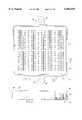
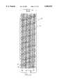
- FIG. 8is a bottom plan view of the receptacle shown in FIG. 1 before the placement of solder balls thereon;
- FIG. 9is a bottom plan view of the receptacle shown in FIG. 8 after placement of the solder balls thereon;
- FIG. 10is a detailed cut away view of area XII in FIG. 1;
- FIG. 11is an enlarged view of the cut away area in FIG. 4;
- FIG. 12is an enlarged view of the cut away area in FIG. 10;
- FIG. 13is an enlarged cross sectional view through 13--13 in FIG. 10;
- FIG. 14is a top plan view of a second preferred embodiment of a receptacle connector of the present invention.
- FIG. 15is an end view of the receptacle shown in FIG. 14;
- FIG. 16is a top plan view of a second preferred embodiment of a plug connector of the present invention.
- FIG. 17is an end view of the plug shown in FIG. 16;
- FIG. 18is an end view of the mated receptacle and plug shown in FIGS. 14-17;
- FIG. 19is a top plan view of a receptacle used in a third preferred embodiment of a receptacle connector of the present invention.
- FIG. 20is an end view of the receptacle shown in FIG. 14;
- FIG. 21is a top plan view of the plug element of the third preferred embodiment of a plug connector of the present invention.
- FIG. 22is an end view of the plug element shown in FIG. 2;
- FIG. 23is an end view of the mated receptacle and plug shown in FIGS. 19-22;
- FIG. 24is a side cross sectional view in fragment of another embodiment of a connector according to the present invention.
- FIG. 24ais a fragmentary view of a portion of the structure of FIG. 24 modified to form a deeper recess
- FIG. 25is a front cross sectional view in fragment of the connector shown in FIG. 24 in which the plug and receptacle are unmated;
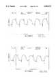
- FIGS. 26a and 26bis a graph showing temperature versus time and distance during solder reflow in Examples 1 and 2 of the method of the present invention
- FIGS. 27a-27fare laser generated profiles of the product of Example 3 of the method of the present invention.
- FIGS. 28a and 28bare x-ray photographs showing the product of Example 4 of the method of the present invention.
- FIGS. 28c and 28dare electron microscope photographs showing the product of Example 4 of the method of the present invention.
- FIG. 29is a view similar to FIG. 10 in which the ground and power contacts have been omitted;
- FIG. 30is a cross sectional view through XXXI--XXXI in FIG. 13;
- FIG. 31is a computer generated representation of predicted stresses in an insulative housing similar to those illustrated in the preferred embodiments of the present invention.
- FIG. 32is a graph of contact retention force as a function of the amount of deformation (compression) in a rib of the insulative housing as is shown in FIG. 29;
- FIG. 33is a front elevational view of a receptacle signal contact used in a preferred embodiment of the connector of the present invention.
- FIG. 34is a front elevational view of a plug signal contact used in a preferred embodiment of the connector of the present invention.
- FIG. 35is a front elevational view of a receptacle ground/power contact with carrier strip used in a preferred embodiment of the connector of the present invention.
- FIG. 36is a front elevational view of a plug ground/power contact with carrier strip used in a preferred embodiment of the connector of the present invention.
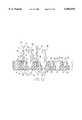
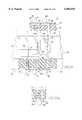
- a set of intermating connectorsaccording to a first embodiment of a high density connector of the present invention includes a receptacle which is shown generally at numeral 10.
- a base section of the receptacleis shown generally at numeral 12.
- the baseis preferably formed by molding an appropriate insulating polymeric material capable of withstanding SMT reflow temperatures, for example, liquid crystal polymer (LCP).
- LCPliquid crystal polymer
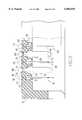
- this elementincludes a base wall 14 having an exterior side 16 and an interior side 18. On the exterior side there are outer recesses as, for example, recesses 20, 22, 24, 26 and 28 (FIG. 12).
- inner contact receiving recessesOn the interior side there are inner contact receiving recesses as, for example, recesses 30, 32, 34, 36 and 38. Connecting these inner and outer recesses are medial slots as, for example, slots 40, 42, 44, 46 and 48.
- Each of the outer recesseshas a base wall and a lateral wall as, for example, base wall 50 and lateral wall 52 (FIG. 12).
- Each of the inner signal contact receiving recesseshas a base wall and intersecting lateral walls as, for example, base wall 54 and lateral walls 56 and 58.
- Each of the inner ground or power contact receiving recessesalso has a base wall and diagonal lateral walls as, for example, base wall 60 and lateral walls 62 and 64.
- the above described inner and outer recesses and connecting medial slotsreceive ground/power contacts or signal contacts.
- the ground or power contactspreferably have an upper section, shown generally at numeral 66, formed of two contacting forks 68 and 70. Each of these forks has a converging section 72, a contact point 74 and an outwardly diverging or lead-in section 76.
- the ground or power contactsalso include a medial section 78 passing through the lower wall of the receptacle and a lower section 80 that extends into the outer recess.
- a solder ball 82is fused onto lower section 80, as will be described below.
- Each of the signal contactsincludes an upper section shown generally at numeral 84 preferably having a contact projection 86, a lead-in bend 88 and a stiffening rib 90.
- the signal contactsalso include a medial section 92 which passes through the lower wall of the receptacle.
- Each signal contactincludes a lower section 98 (FIG. 13) extending into the outer recess for example, recess 22 in FIGS. 12-13, where a solder ball 100 is fused to lower section 98 as will be explained below.
- the base section of the receptacleincludes latching structures, for example, as is shown generally at numeral 102.
- This latching structureincludes an upward tab 104 which is superimposed over a vertical groove 106 and which has an outward projection 108.
- the base section of the receptaclealso has other similar latching structures 110, 112 and 114.
- the receptaclealso includes an upper section shown generally at 116 which is superimposed over the base section. This upper section has a top wall 118 and a peripheral side wall 120. This upper section is fixed to the base section by means of latching structures as is, for example, shown generally at numeral 122.
- Each of these latching structureshas a side wall recess 124 and a U-shaped latch 126 which extends downwardly from the top wall and is spaced from the side wall recess.
- the tab 104fits between the U-shaped latch 126 and the side wall recess 124 to enable the U-shaped latch to engage the outward projection 108 on the latching structure 102 of the base section.
- the upper sectionincludes other similar latching structures 128, 130 and 132 which engage, respectively, latching structures 110, 112 and 114 on the base section.
- the upper section 116 or the base 102also may have mounting brackets 134 and 136 which have fastener apertures 138 and 140, respectively.
- signal contact access aperturesas, for example, apertures 142 and 144. These access apertures are arranged in a plurality of rows corresponding to the rows of signal contacts in the base section. Interposed between these rows of signal contact access apertures are elongated ground or power contact access slots as, for example, slots 146 and 148.
- the upper section 116forms a mating interface between receptacle 10 and a mating plug 150 described below.
- the plug element of the connectoris shown generally at numeral 150.
- the plugincludes a base wall 152 and a peripheral side wall 154. There are opposed gaps 156 and 158 in the side wall and there is an open side 160 in opposed relation to the base wall. Projecting laterally from the plug are mounting brackets 162 and 164 having fastener receiving apertures 166 and 168 respectively, that are alignable with the fastener receiving apertures 138, 140 in the mounting brackets of the receptacle.
- inner signal contact receiving recessessuch as recess 170.
- inner power or ground contact receiving recessessuch as recess 172.
- outer signal contact receiving recessessuch as recess 174, and outer power or ground contact receiving recesses, as at recess 176.
- medial slots 178 and 180Mounted in the power/ground contact receiving recesses via the medial slots 180 are power or ground contacts, shown generally at numeral 182.
- Each contact 182has an elongated inner section 184, an elongated medial section 186, which is mounted in base wall 152, and an outer section 188 extending into recess 176.
- a solder ball 190is fused onto section 188.
- the outer section 188 and the solder ballare partially contained in the outer recess 176.
- the plugalso includes a plurality of signal contacts 192. These signal contacts each have an inner section 194, a medial section 196 mounted in the base wall, and a terminal tab 198 extending into recess 174.
- a solder ball 200is fused onto terminal tab 198. Again it will be observed that this outer section and the solder ball are partially contained in the outer recess as at 170.
- the plug described aboveis mounted on a circuit substrate, such as a rigid PWB 202, and the receptacle is mounted on a similar PWB 204.
- the plug and receptaclethereby form a board to board interconnection, as illustrated in FIG. 6.
- the plughas a two dimensional array of signal contacts, such as 192 onto which are fused solder balls 200 and a plurality of ground/power contacts, such as contacts 192, onto which are fused solder balls 190.
- the solder ballsare also fused to the PWB 202 to fix the entire plug to the PWB and effect electrical contact between the signal contacts and ground or power contacts in the plug and the PWB.
- solder balls 100are fused onto receptacle signal contacts 84 and those solder balls are fused to the PWB 204.
- Receptacle ground/power contacts 66are mounted in slot 134 and are fused to solder balls 82 and these solder balls are fused to PWB 204.
- the plugis aligned with the receptacle so that the peripheral side wall 154 of the plug overlaps the peripheral side wall 120 of the upper section 118 of the receptacle.
- FIG. 7ashows, after initial alignment, the ground/power contacts in the plug initially entering the ground/power contact receiving slots in the receptacle and engaging the corresponding power/ground contacts in the receptacle.
- the signal contactshave entered the signal contact slots in the receptacle.
- FIG. 7bshows the signal contacts in the plug initially engaging the corresponding signal contacts in the receptacle and the power/ground contacts in the plug becoming further engaged between the opposed leaves of the power ground contacts in the receptacle.
- FIG. 7cshows that the signal contacts in the plug being fully engaged with the signal contacts in the receptacle.
- the power/ground contacts in the plughave become positioned at the base of the fork of the power/ground contacts in the receptacle.
- the exterior side 16 of the base section 12 of the receptacleis shown prior to the application of the solder balls.
- the terminal tabs of the signal contactsfor example, terminal tab 82
- of the power ground contactsfor example terminal tab 98
- a quantity of solder paste of appropriate compositionis applied to substantially fill each outer recess.
- the solder ballsare then applied over the outer or mounting surface of the base.
- the outer recessesare smaller in transverse extent than the solder balls, so that the solder balls are supported on the edges of the recesses, at a position near the terminal tabs of the contacts.
- a recessthat is round or the shape of a regular polygon in cross-section is preferred.
- the solder pasteaids in holding a solder ball in each of the exposed recesses as is shown in FIG. 9, where, for example, solder ball 82 is shown in recess 20 and solder ball 100 is shown in recess 22. Additional solder balls, 230, 232 and 234 are shown, for example, in recesses 24, 26 and 28.
- a solder ballwill be positioned in all of the outer recesses of the receptacle. It will also be understood that the exterior side of plug will be substantially identical to the exterior side of the receptacle before placement of the solder balls as is shown in FIG. 8 and after emplacement of the solder balls as is shown in FIG. 11. After emplacement of the solder balls in the outer recesses, the connector is subjected to a reflow process to fuse the solder balls onto the terminal tabs. The exterior sides of the connectors, together with the solder balls and particularly the outer surfaces of the solder balls, form a substantially planar mounting interface, along which the connector is mounted onto a supporting circuit substrate, such as a PWB.
- a supporting circuit substratesuch as a PWB.
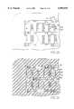
- FIGS. 10 and 13show a variant of the FIG. 1 embodiment wherein, instead of the forked receptacle contacts 66, oppositely disposed pairs 66a and 66b of blade type contacts engage the ground/power terminals 182.
- FIGS. 14-18illustrate a second preferred embodiment of a set of intermating connectors of this invention.
- this setincludes a receptacle shown generally at numeral 236.
- This receptacleincludes an insulative housing shown generally at 238 which has an inner side 240, a lateral side 242 and an exterior side 244.
- the housingalso includes opposed alignment projections 246 and 248.
- contacts 250, 251 and 252each having sections which bow away from each other and then converge to a contact point from which they then again diverge.
- Contacts 251are mounted on base 231 in the same manner as the embodiments shown in FIGS. 1-13.
- solder ballssuch as solder ball 254, are mounted to the board side of contacts 251 in the same manner as described above.
- the setalso includes a plug shown generally at 258 which includes an insulative housing shown generally at 260 having an inner side 262, a peripheral lateral side 264 and an exterior side 266. At one end of the housing there are a pair of vertical end walls 268 and 270 with a medial end recess 272. At the opposed end of the housing there are another pair of end walls 274 and 276 with a medial end recess 278. Extending from the inner side of the housing there are a plurality of contacts as at contact 280 that extend from recesses as at 282.
- each of these contactsis fused a solder ball 284. It will also be seen that these contacts are positioned in a staggered arrangement. For example, contact 286 is offset with respect to contact 280, so rows of contacts can be spaced closer together to increase contact density.
- each contact in the plugsuch as contact 280 is vertically aligned with one of the pairs of converging contacts, such as contacts 250 and 252, in the receptacle and is interposed between these converging contacts.
- the alignment projections 246 and 248also engage the end recesses 272 and 278 in the plug.
- the separate ground/power contacts used in the FIGS. 1-13 embodimentare not present. Such functions can, if desired, be incorporated into the undivided contacts pairs.
- FIGS. 19-23show a third preferred embodiment of a set of intermating connectors.
- the plugis shown generally at numeral 290.
- This plugincludes a housing generally 292 having a base wall 294 and a peripheral lateral wall 296, as well as opposed alignment projections 298 and 300.
- the base wall of the housinghas an inner side 302 and an outer side 304.
- Signal contacts, such as contact 306,extend from inner side 302. It will be seen that the signal contacts are also staggered or offset in alternate rows, to increase contact density.
- the plugalso includes ground or power contacts 310, 312, 314 and 316 arranged adjacent each of the sides of the plug parallel to one side of the lateral wall.
- the receptacleis shown generally at numeral 322 and has an insulative housing 324 that includes a base wall 326, a peripheral lateral wall 328 and alignment projection receiving recesses 330 and 332.
- the base wallalso has an exterior side 334 and an inner side 336. Projecting from the inner side are signal contacts such as contacts 338 and 340. The contacts in adjacent transverse rows are also axially offset to allow an increase in contact density. Parallel to each side of the peripheral wall there are lateral power or ground contacts 342, 344, 346 and 350.
- solder ball 352On the exterior side of the base wall there are for each signal contact a solder ball, such as solder ball 352. There are also solder balls, such as at solder ball 354, for attaching each of the power or ground pins. Referring to particularly to FIG. 23, it will be seen that at the plug 290 engages receptacle 322.
- componentssuch as electrical connectors, that are to be mounted on circuit substrates by SMT techniques must meet very demanding specifications for coplanarity. If tight tolerances on coplanarity, usually on the order of about 0.003 to about 0.004 inch, are not maintained, manufacturers experience undesirably high failure rates resulting from faulty solder connections. Variations in the distance of a surface mount portion of a contact from the circuit substrate can result from variations in the location of the contact in the insulative housing occurring as a result of the contact insertion process and from deformation of the housings, resulting in bowing or warping of the mounting interface of the connector body.
- Connectors made in accordance with the present inventionare capable of attaining strict coplanarity requirements by use of features that carefully locate and size the fusible bodies used for bonding the connector to a substrate and by the use of contact securing arrangements that prevent accumulations of stresses in the connector housing that tend to distort the housing.
- the metal contactsare secured in insulative housings in a manner to avoid the inducing of stress in the body of the housing.
- This securingis achieved by the use of a shaped slot or opening into which a securing portion of the contact is inserted.
- the slothas a shape that closely conforms in shape and dimensions to all the surfaces of the contact but one.
- the wall of the slot facing that one surfacehas an integrally molded lateral projection projecting into the slot. The distance between the distal end of the projection and the opposing wall of the slot is less than the thickness of the contact.
- the projectioncomprises a pyramidal rib integrally formed on one of the side walls of the slot.
- a signal contact 494is retained in slot 496 and abuts against rib 498.
- the ribhas a planar surface 500, where it engages the contact 494, and opposed oblique sides 502 and 504.
- the contact 494is securely retained in the slot by engagement with the back and side edges of the slot 496 and rib 498.
- the portion of the rib adjacent surface 500is free to deform as contact 494 is forced into slot 496, thereby relieving any stresses that result from contact insertion.
- a power/ground contactis retained in slot 508 and bears against deformable rib 510.
- the ribhas a distal portion 512, where it abuts against the contact, and opposed oblique sides 514 and 516.
- there is also an opposed ribas, for example, rib 518.
- This opposed insulative ribalso has a distal portion 520 and oblique sides 522 and 524.
- the opposed deformable ribscan be used for securing larger contacts and for centering the contact in the slot.
- FIG. 31which was generated using ANSYS stress analysis software available from Ansys, Inc. of Houston, Pa. shows that by use of the contact securing arrangement illustrated in FIGS. 29 and 30, high levels of stress are essentially isolated in the ribs, and do not extend substantially beyond the contact mounting slots thereby significantly reducing the risk of warpage or twisting of the housing which could otherwise result from a large number of contact insertions.
- the units for the various stress areas shown in FIG. 31is N/mm 2 and the mm is the unit for displacement shown.
- FIG. 32shows that, for a typical contact 494, increases in deformation (compression) of the distal portion of the deformable rib up to about 0.0004 inch resulted in an increasing retention force between the contact and the housing, resulting from the normal force imparted on the contact by the rib. After 0.0004 inches of deformation (compression), only minor increases in retention force resulted.
- the termination tab of each contactis positioned in a recess.
- the outer recessesare substantially uniform in size and shape. These recesses provide several features of importance with respect to the present invention.
- the recessescan receive a highly uniform amount of solder paste placed therein, for example, by a simple deposit and squeegee operation. Thus the amount of solder available for securing each solder ball onto a contact is substantially uniform.
- the recesseslocate the position of each solder ball in the lateral X-Y directions prior to attachment of the solder balls onto the contacts.
- the recessesalso locate the solder balls in the Z direction with respect to the bottom surface of the housing and the distance of the solder ball from the terminal tabs of the contacts.
- the nominal extension of the tab into the recessis set so that at the maximum of the tolerance for extension of the tab into the recess, the tab does not touch the solder ball and thereby influence its Z direction location.
- fusing of the solder ball onto the contact tabis assured by having a relatively uniform and adequate amount of solder, from the solder paste, in the recess. Any variation in the distance between the contact tab and the solder ball is absorbed by the variable volume of solder paste placed in the recess.
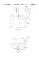
- contacts 526 and 528are shown attached to a carrier strip 530.
- the contactshave a contact engagement area 532 usually plated with non-oxidizing metals such as gold, palladium or alloys of palladium.
- the contactsalso have a central area 534, a portion of which forms the contact retention area in the housing.
- An anti-solder wicking or non-solder wettable materialis applied to the central area 532.
- One preferred material for this purposeis nickel plating.
- the solder resistant feature of this nickel plated arearesults from or is enhanced by the oxidation of the nickel after plating, for example, by exposure to ambient air for several days.
- the nickel or nickel oxide barrierprevents or reduces solder wicking in such contacts.
- the platinghave a thickness of from 10 ⁇ in to 10 ⁇ in and more preferably about 50 ⁇ in.
- Other solder wick resistant materialsare believed to be usable for this purpose, such as flourine containing solder resist coatings.
- the contact tab area 536may preferably be plated with a solder receptive material such as gold, tin or tin alloys.
- the entire contactwill be plated with nickel.
- a solder wettable metal layerselectively plated on the lower section.
- an electroplated layer of chromiumcan be substituted for the nickel layer. Referring to FIG.
- plug signal contacts 538 and 540are shown attached to a carrier strip 542.
- Each of these contactshas a gold plated tab area 544, a nickel plated central retention and anti-wicking area 536 and a precious metal plated engagement area 548.
- the ground/power contact 550is shown attached to carrier strip 552. This contact has a lower gold plated tab area 554, a nickel plated central anti-wicking area 556 and an upper gold plated contact engagement area 558.
- Another feature of ground/power contact 550 which is also found to reduce wickingis a series of notches in the tab area 554 such as notches 560, 562 and 564.
- Another feature of ground/power contact 550 which was included in embodiments disclosed aboveis vertical slots such as slot 566.
- a plug ground/power contact 568which has a lower gold plated tab area 570, a nickel plated central anti-wicking area 572 and an upper gold plated area 574. It will be seen that ground/power contact 568 does not have a separate carrier strip, but it does have apertures such as aperture 576 which allow the contact itself to serve this carrier function. With each of the contacts described above it will be understood that tin or other solder wettable material may be substituted for gold in the lower area.
- the width of the lower gold plated tab areaas is, for example, shown at w 1 in FIG. 37 will preferably be from about 0.1 mm to about 0.25 mm.
- the width of the nickel plated central area as is shown, for example, at w 2 in FIG. 37will preferably be from about 0.1 mm to about 1 mm.
- the receptacle of this connectoris shown generally at numeral 324.
- This receptaclehas a base wall 326 having an exterior side 328 and an interior side 330.
- On the exterior sidethere are recesses such as at recesses 332, 334, 336, 338, and 340, (FIG. 25) 342 and 344 (FIG. 24).
- Each of these recessespreferably has an oblique base wall 360 having a rounded surface 362.
- the receptaclehas substantially the same construction as the receptacle illustrated in FIGS. 1 and 2. It includes an upper section 436 secured on base 326 in a suitable manner, preferably by latches (not shown) as discussed with respect to FIGS. 1 and 2.
- the upper section or cover 436has a plurality of openings, such as openings 452 and 460, for receiving individual contacts from a mating plug or slots, such as slots 454, 456, 468 (FIGS. 25) for receiving ground or power contacts from the mating plug.
- the signal contacts, such as contact 408, and ground/power contactsare of a form substantially as described with respect to any of the previous described embodiments.
- the ground contact 382(FIG. 25) has a lower section 384 from which there is a tab 386.
- This contactalso has an upper section shown generally at numeral 388 which is made up of forks 390 and 392. Each of these forks has a converging section 394 and an outwardly diverging lead-in section 396.
- Each signal contactsuch as contact 408, has an upper section 410 with a forward projection 412 and rearward bend 414.
- the signal contactalso has a medial section 416 where it engages the insulative housing and a lower tab 418 located in recess 334.
- the tab 386 of ground contact 382 and the tab 418 of signal contact 408are formed by bending the tail portions of the respective terminals about the surfaces 362, after the contacts are inserted into base 326.
- Each surface 362serves as bending mandrel for an associated contact tail.
- the tailsare bent to the extent of the oblique surface 360 and are allowed to spring back so that the tabs are transverse to the longitudinal axis of the contact and are substantially parallel to the surface 328. This assures a high degree of coplanarity of the tabs.
- solder pasteis applied to the outside surface of each tab. Solder balls, such as 398, 400, 402, 404, 406 (FIG. 25), 426 and 428 (FIG.
- solder ball 398ais located partially within the recess 334a and is stabilized by the edges thereof, as previously discussed especially with respect to FIGS. 12 and 13. As a result, when solder balls of highly uniform size are used, these arrangements can yield finished connectors that exhibit coplanarity of the contacts across the mounting interface.
- a plug having generally the same construction as the plugs previously describedis shown generally at numeral 430. It includes a base wall 432 having an exterior side 434 and an interior side 436. On the exterior side there are recesses as at recess 438, 440, 442, 444 and 446. Each of these recesses has an oblique base wall 448 and a curved wall 450. Connecting with each of these recesses are contact slots 452, 454, 456, 458 and 460.
- the plugalso has a number of power/ground contacts as, for example, is shown generally at numeral 462. Each of these contacts has a contact section 464 that engages the forks of the ground/power contacts of the receptacle.
- the plugalso includes a number of signal contacts as, for example, is shown generally at numeral 476. Each of these signal contacts includes a contact section 478 which engages the signal contacts in the receptacle, a medial section 480 where it engages the housing and a solder ball tab 482 for receiving a solder ball. Other signal contacts as at 486 and 488 engage respectively other solder balls as at 490 and 492.
- the solder ball tabsare formed and solder balls 470, 474, 484, 490 and 492 are applied to the plug in substantially the same manner as previously described with respect to the receptacle.
- the conductive elementwill preferably be a solder ball.
- the fusible elementcan also have a shape other than a sphere.
- the solder ball or other conductive elementwill also preferably have a diameter which is from about 50 percent to 200 per cent of the width of the recess. This diameter will also preferably be related to the depth of the recess and be from 50 percent to 200 per cent of that depth.
- the volume of the solder ballwill preferably be from about 75 percent to about 150 percent of the volume of the recess and, more preferably, will be about the same volume as the recess.
- the contact tabwill extend into the recess by a sufficient amount to present adequate surface area for the solder ball to fuse to, and will usually preferably extend into the recess from about 25 percent to 75 percent and more preferably to about 50 percent of the depth of the recess as previously mentioned.
- the recessesordinarily will be circular, square or the shape of any other regular polygon in cross section.
- the conductive elementis solder, it will preferably be an alloy which is in the range of about 90 Pb and 10% Sn to about 55% Pb and 45% Sn. More preferably the alloy will be eutectic which is 63% Pb and 37% Sn and has a melting point of 183° C.
- solder alloywith a higher lead content would be used for mating to materials such as ceramics.
- the "hard” solder ballwill “mushroom” or deform slightly as it softens under typical SMT conditions, but will not melt.
- a “soft” eutectic ballis used for attachment to PCB's and will usually reflow and reform itself under typical SMT conditions.
- solders known to be suitable for electronic purposesare also believed to be acceptable for use in this method. Such solders include, without limitation, electronically acceptable tin-antimony, tin-silver and lead-silver alloys and indium. Before the solder ball or other conductive element is positioned in a recess, that recess would usually be filled with solder paste.
- a body of material which is not fusible at SMT temperaturesmay be attached by reflow of the solder paste in the recesses onto the contacts.
- the connector mounting interfacewould comprise a plurality of infusible spheres in a tightly coplanar array. Such a connector would be secured on a substrate by conventional SMT techniques.
- solder pastes or creamsincorporating any conventional organic or inorganic solder flux may be adapted for use in this method
- a no clean solder paste or creamis preferred.
- solder pastes or creamswould include a solder alloy in the form of a fine powder suspended in a suitable fluxing material. This powder will ordinarily be an alloy and not a mixture of constituents. The ratio of solder to flux will ordinarily be high and in the range of 80%-95% by weight solder or approximately 80% by volume. A solder cream will be formed when the solder material is suspended in a rosin flux.
- the rosin fluxwill be a white rosin or a low activity rosin flux, although for various purposes activated or superactivated rosins may be used.
- a solder pastewill be formed when a solder alloy in the form of a fine powder is suspended in an organic acid flux or an inorganic acid flux.
- organic acidsmay be selected from lactic, oleic, stearic, phthalic, citric or other similar acids.
- Such inorganic acidsmay be selected from hydrochloric, hydroflouric and orthophosphoric acid.
- Cream or pastemay be applied by brushing, screening, or extruding onto the surface which may advantageously have been gradually preheated to ensure good wetting.
- wicking of the solder onto the contactis significantly reduced when a solder paste or cream is used, it is believed that paste type solder flux alone may also be used when a suitable, passivation agent is used.
- a suitable passivation agentswould include fluoride containing solder resist coatings such as FLOURAD which is available from the 3M Corporation.
- Heatingis preferably conducted in a panel infra red (IR) solder reflow conveyor oven.
- the solder elementwould ordinarily be heated to a temperature from about 183° to about 195° C. but, depending on the material of the housing, solders having melting temperatures may be used.
- the conveyor ovenwould preferably be operated at a rate of speed from about 10 to 14 inches per second and would be moved through a plurality of successive heating phases for a total time of about 5 minutes to about 10 minutes.
- contacts and solder elementsPrior to being inserted into the conveyor oven the connector housing, contacts and solder elements may be preheated at an elevated temperature for at least an hour. In the conveyor oven a temperature profile would be developed based on an appropriate peak temperature, maximum slope and time above reflow temperature. Peak temperature is the highest temperature reached by the housing.
- peak temperaturewould usually be between 185° C. and 195° C.
- Maximum slopeis measured in ° C./sec. and specifies how fast the connector housing temperature is allowed to change, so as to avoid warping or bending.
- maximum positive slopewill preferably initially be from about 2° C./sec to 15° C./sec.
- negative slopewill preferably be -2° C./sec to -15° C./sec.
- An important aspect of the method of this inventionis that time above reflow is minimized. Time above reflow is a measure of how long the solder element remains in its liquid phase.
- rise time of temperature as measured on the board between 180° C. and 200° C. and fall time of temperature as measured on the board between 200° C. and 180° C.will both be from about 10 seconds to about 100 seconds. While not intending to be bound by any particular theory, it is believed that during such relatively short periods of time, surface tension of the liquid solder element will restrain the liquid solder from flowing through the contact receiving slot in the base of the recess. After such periods of time, however, the liquid solder will begin to flow through the contact receiving slot and wick up the contact.
- the housing materialwill be wholly aromatic liquid crystal polyester (LCP) with characteristics of high glass transition temperature, low thermal coefficient, low moisture absorption, high fracture toughness, good flow and low viscosity, high temperature and high flash point.
- LCPwholly aromatic liquid crystal polyester
- FIGS. 1-18An insulative housing for a connector plug and receptacle substantially is described above in connection with FIGS. 1-18 was made. Contacts also substantially in accordance with that description were also positioned in the housing. These contacts were beryllium copper and were plated with gold over their entire surface area to a thickness of 30 microns.
- the housing materialwas DUPONT H6130 liquid crystal polymer (LCP).
- LCPliquid crystal polymer
- the length and width of the plugwere respectively 52.5 mm (including mounting brackets) and 42.36 mm.
- the recesses on the exterior surfaces of the plug and receptacle housingwere cross sectionally square having a side dimension of 0.62 mm and a depth of 0.4 mm. About 2 mm of the contact extended into the recess.
- the plug and receptaclewere then treated with FLUORAD, a solder anti-wicking material available from 3M Corporation. After such treatment the plug and receptacle were then dried in a convection oven for 2 hours at 105° C. The plug and receptacle were then positioned on separate circuit boards made of conventional reinforced epoxy printed circuit board material, having thicknesses of 0.061 inches. Referring to FIG. 9, a thermocouple was placed on the exterior surface of the plug in position T. Another thermocouple was centrally positioned upon the supporting board surface adjacent the plug. Both the plug and the receptacle were then treated in a panel-infrared (IR) conveyer solder reflow oven.
- IRpanel-infrared
- the plug and receptaclewere moved through six zones in the reflow oven.
- the conveyor speedwas 13 in/min. Heating temperatures in each zone are shown in Table 1.
- Minimum and maximum temperatures for the plug and for the supporting boardare shown in Table 2.
- Both positive and negative maximum slopesare shown in Table 3.
- Rise time and fall time measured on the board between 180° C. and 200° C.are shown in Table 4.
- Temperature by time and distance for the plugis shown in the curve in FIG. 26a wherein the heavy line is the temperature at the thermocouple on the supporting board and the light line is temperature at the thermocouple on the plug exterior surface.
- FIGS. 26a and 26bAnother connector was made using essentially the same conditions as were described in Examples 1 and 2 except that the specific curves shown in FIGS. 26a and 26b may have been somewhat different because of atmospheric conditions.
- PRSLaser Point Range Sensor
- FIG. 9these locations are identified as areas 27a and 27b when the laser was directed from L 1 , as areas 27c and 27d when the laser was directed from L 2 and as areas 27e and 27f when the laser was directed from L 3 .
- PRSLaser Point Range Sensor
- FIGS. 26a and 26bAnother connector was made essentially according to the conditions described in Examples 1 and 2 except because of atmospheric conditions the specific curves shown on FIGS. 26a and 26b may have been somewhat different. In almost all cases solder balls were satisfactorily fused to the contact leads and solder balls were of an acceptably uniform height above the plane of the exterior surfaces of the plug and receptacle on visual inspection. A stencil with a pattern matching the solder balls on both the plug and receptacle was used to apply solder paste onto conductive solder pads on two different circuit boards having a thickness of 0.061 inches. The plug was positioned on one circuit board and the receptacle was positioned on the other.
- FIGS. 28a and 28bA photograph showing these x-rays of selected solder balls are attached respectively at FIGS. 28a and 28b.
- Cross sectional electron microscope photographswere taken to show the fusing of the solder balls to the signal contact leads and the fusing of the solder balls to the printed circuit board material. These electron microscope photographs are shown respectively at FIGS. 28c and 28d. There was only one short between adjacent signal contacts and good connections were made between the contacts and the solder balls and between the solder balls and the boards at all other points.
Landscapes
- Engineering & Computer Science (AREA)
- Manufacturing & Machinery (AREA)
- Coupling Device And Connection With Printed Circuit (AREA)
Abstract
Description
TABLE 1 ______________________________________ Temperature (°C.) Ex-ample ZONE # 1 #2 #3 #4 #5 #6 ______________________________________ 1UPPER 350 Unheated 275 230 310Unheated 1 LOW- Un- Unheated 275 230 310 Unheated ER heated 2UPPER 350 Unheated 275 230 310 Unheated 2 Lower Un- Unheated 275 230 710 Unheated heated ______________________________________
TABLE 2 ______________________________________ Connector Board Max Temp Time (Min. Max Temp Time Example (°C.) & Sec.) (°C.) (Min & Sec) ______________________________________ 1 188 4:37.6 -- -- 1 -- -- 232 4:19.8 2 191 4:53.2 -- -- 2 -- -- 229 5:10.4 ______________________________________
TABLE 3 ______________________________________ Positive and Negative Maximum Slope °C. (Sec) Connector Board Time Reached Time Reached Example Max (Min & Sec) Max (Min & Sec) ______________________________________ 1 +2 0:50.4 +2 0:30.4 1 -2 6:45.2 -3 5:58.8 2 +3 7:08.0 +3 1:14.8 2 -15 6:13.8 -7 6:14.0 ______________________________________
TABLE 4 ______________________________________ Rise Time and Full Time Between 180° C. and 200° C. (Measured on Board) Example Rise Time (Min & Sec) Fall Time (Min & Sec) ______________________________________ 1 0:28.8 0:15.2 2 1:31.6 0:40.6 ______________________________________
TABLE 5 ______________________________________ POSITION HEIGHT (.001 in.)GROUP 1 2 3 4 5 ______________________________________ 27a 18.1 18.9 19.5 19.6 19.1 27b 19.2 18.5 17.6 18.5 18.0 27c 20.4 21.1 21.6 21.1 21.4 27d 19.9 20.1 20.1 21.2 20.5 27e 18.2 18.9 19.3 18.2 18.7 27f 19.1 18.2 19.0 18.2 18.9 ______________________________________
Claims (26)
Priority Applications (51)
| Application Number | Priority Date | Filing Date | Title |
|---|---|---|---|
| US08/778,398US6093035A (en) | 1996-06-28 | 1996-12-31 | Contact for use in an electrical connector |
| TW086113845ATW406454B (en) | 1996-10-10 | 1997-09-23 | High density connector and method of manufacture |
| SG1997003496ASG71046A1 (en) | 1996-10-10 | 1997-09-23 | High density connector and method of manufacture |
| PCT/US1997/018066WO1998015989A1 (en) | 1996-10-10 | 1997-10-07 | High density connector and method of manufacture |
| AU51454/98AAU5145498A (en) | 1996-10-10 | 1997-10-07 | High density connector and method of manufacture |
| CN2003101026354ACN1510788B (en) | 1996-10-10 | 1997-10-09 | electrical connector |
| CNB971204144ACN1200483C (en) | 1996-10-10 | 1997-10-09 | High density electrical connector and method of making same |
| CN2005100563746ACN1655405B (en) | 1996-10-10 | 1997-10-09 | High density electrical connector |
| CA002267293ACA2267293C (en) | 1996-10-10 | 1997-10-10 | High density connector and method of manufacture |
| DE29724718UDE29724718U1 (en) | 1996-10-10 | 1997-10-10 | High density connector assembly |
| DE69737252TDE69737252T2 (en) | 1996-10-10 | 1997-10-10 | High density connector and manufacturing process |
| AT03000664TATE340424T1 (en) | 1996-10-10 | 1997-10-10 | HIGH CONTACT DENSITY CONNECTORS AND MANUFACTURING PROCESS |
| EP05020003AEP1617519B1 (en) | 1996-10-10 | 1997-10-10 | High density connector |
| CA002497606ACA2497606C (en) | 1996-10-10 | 1997-10-10 | High density connector and method of manufacture |
| AU48156/97AAU730360B2 (en) | 1996-10-10 | 1997-10-10 | High density connector and method of manufacture |
| DE69736682TDE69736682T2 (en) | 1996-10-10 | 1997-10-10 | High density connector and manufacturing process |
| EP03000661AEP1311029B1 (en) | 1996-10-10 | 1997-10-10 | High density connector and method of manufacture |
| EP04006131AEP1441417A3 (en) | 1996-10-10 | 1997-10-10 | High density connector and method of manufacture |
| PL377458APL192431B1 (en) | 1996-10-10 | 1997-10-10 | Method of manufacture an electrical connector |
| EP03000664AEP1311032B1 (en) | 1996-10-10 | 1997-10-10 | High density connector and method of manufacture |
| AT03000663TATE340423T1 (en) | 1996-10-10 | 1997-10-10 | HIGH CONTACT DENSITY CONNECTORS |
| DE29724822UDE29724822U1 (en) | 1996-10-10 | 1997-10-10 | High density connector assembly |
| DE29724720UDE29724720U1 (en) | 1996-10-10 | 1997-10-10 | High density connector assembly |
| DE69736721TDE69736721T2 (en) | 1996-10-10 | 1997-10-10 | High density connector |
| DE69736722TDE69736722T2 (en) | 1996-10-10 | 1997-10-10 | High density connector |
| EP03000663AEP1311031B1 (en) | 1996-10-10 | 1997-10-10 | High density connector |
| HU0600083AHU229998B1 (en) | 1996-10-10 | 1997-10-10 | Electric connector |
| DE69736720TDE69736720T2 (en) | 1996-10-10 | 1997-10-10 | High density connector |
| EP03000662AEP1311030B1 (en) | 1996-10-10 | 1997-10-10 | High density connector |
| CA002455080ACA2455080C (en) | 1996-10-10 | 1997-10-10 | High density connector and method of manufacture |
| DE29724719UDE29724719U1 (en) | 1996-10-10 | 1997-10-10 | High density connector assembly |
| DE29724717UDE29724717U1 (en) | 1996-10-10 | 1997-10-10 | High density connector assembly |
| HU9904238AHU229923B1 (en) | 1996-10-10 | 1997-10-10 | High density connector and method of manufacture |
| AT97117583TATE352112T1 (en) | 1996-10-10 | 1997-10-10 | HIGH CONTACT DENSITY CONNECTORS AND MANUFACTURING PROCESS |
| EP97117583AEP0836243B1 (en) | 1996-10-10 | 1997-10-10 | High density connector and method of manufacture |
| BRPI9712296-3ABR9712296B1 (en) | 1996-10-10 | 1997-10-10 | electrical connector; Method for making an electrical connector and Method for minimizing voltage growth within an electrical connector housing. |
| AT03000661TATE339785T1 (en) | 1996-10-10 | 1997-10-10 | HIGH CONTACT DENSITY CONNECTORS AND MANUFACTURING PROCESS |
| AT03000662TATE340422T1 (en) | 1996-10-10 | 1997-10-10 | HIGH CONTACT DENSITY CONNECTORS |
| PL332869APL192236B1 (en) | 1996-10-10 | 1997-10-10 | Electric switch for high switching rates and method of making same |
| CA002404792ACA2404792C (en) | 1996-10-10 | 1997-10-10 | High density connector and method of manufacture |
| PCT/US1997/018354WO1998015991A1 (en) | 1996-10-10 | 1997-10-10 | High density connector and method of manufacture |
| RU99109028/09ARU2208279C2 (en) | 1996-10-10 | 1997-10-10 | Connector distinguished by high-density disposition of components and its manufacturing process |
| CZ0122299ACZ298529B6 (en) | 1996-10-10 | 1997-10-10 | Electrical connector |
| JP27907697AJP3413080B2 (en) | 1996-10-10 | 1997-10-13 | High density connector and manufacturing method |
| US09/284,230US6325644B1 (en) | 1996-10-10 | 1999-07-07 | High density connector and method of manufacture |
| US09/953,631US7186123B2 (en) | 1996-10-10 | 2001-09-14 | High density connector and method of manufacture |
| KR1020030074088AKR100450547B1 (en) | 1996-10-10 | 2003-10-23 | High density connector and method of manufacture |
| US11/272,212US7168964B2 (en) | 1996-10-10 | 2005-11-10 | High density connector and method of manufacture |
| US11/668,435US7476110B2 (en) | 1996-10-10 | 2007-01-29 | High density connector and method of manufacture |
| US12/352,227US7802999B2 (en) | 1996-10-10 | 2009-01-12 | High density connector and method of manufacture |
| US12/891,469US8167630B2 (en) | 1996-10-10 | 2010-09-27 | High density connector and method of manufacture |
Applications Claiming Priority (4)
| Application Number | Priority Date | Filing Date | Title |
|---|---|---|---|
| US2078796P | 1996-06-28 | 1996-06-28 | |
| US2761196P | 1996-10-10 | 1996-10-10 | |
| US08/728,194US6024584A (en) | 1996-10-10 | 1996-10-10 | High density connector |
| US08/778,398US6093035A (en) | 1996-06-28 | 1996-12-31 | Contact for use in an electrical connector |
Related Parent Applications (2)
| Application Number | Title | Priority Date | Filing Date |
|---|---|---|---|
| US08/728,194Continuation-In-PartUS6024584A (en) | 1996-06-28 | 1996-10-10 | High density connector |
| US08/728,194ContinuationUS6024584A (en) | 1996-06-28 | 1996-10-10 | High density connector |
Related Child Applications (3)
| Application Number | Title | Priority Date | Filing Date |
|---|---|---|---|
| US08/778,380ContinuationUS6079991A (en) | 1996-10-10 | 1996-12-31 | Method for placing contact on electrical connector |
| US08/778,380Continuation-In-PartUS6079991A (en) | 1996-10-10 | 1996-12-31 | Method for placing contact on electrical connector |
| US09/953,631ContinuationUS7186123B2 (en) | 1996-10-10 | 2001-09-14 | High density connector and method of manufacture |
Publications (1)
| Publication Number | Publication Date |
|---|---|
| US6093035Atrue US6093035A (en) | 2000-07-25 |
Family
ID=27361513
Family Applications (1)
| Application Number | Title | Priority Date | Filing Date |
|---|---|---|---|
| US08/778,398Expired - LifetimeUS6093035A (en) | 1996-06-28 | 1996-12-31 | Contact for use in an electrical connector |
Country Status (1)
| Country | Link |
|---|---|
| US (1) | US6093035A (en) |
Cited By (45)
| Publication number | Priority date | Publication date | Assignee | Title |
|---|---|---|---|---|
| US6443750B1 (en) | 1999-08-04 | 2002-09-03 | Fci Americas Technology, Inc. | Electrical connector |
| US20020164838A1 (en)* | 2001-05-02 | 2002-11-07 | Moon Ow Chee | Flexible ball grid array chip scale packages and methods of fabrication |
| US6535105B2 (en) | 2000-03-30 | 2003-03-18 | Avx Corporation | Electronic device and process of making electronic device |
| US20030134450A1 (en)* | 2002-01-09 | 2003-07-17 | Lee Teck Kheng | Elimination of RDL using tape base flip chip on flex for die stacking |
| US20030166312A1 (en)* | 2002-03-04 | 2003-09-04 | Lee Teck Kheng | Methods for assembly and packaging of flip chip configured dice with interposer |
| US20030164548A1 (en)* | 2002-03-04 | 2003-09-04 | Lee Teck Kheng | Flip chip packaging using recessed interposer terminals |
| US20030164540A1 (en)* | 2002-03-04 | 2003-09-04 | Lee Teck Kheng | Semiconductor die packages with recessed interconnecting structures and methods for assembling the same |
| US20030164543A1 (en)* | 2002-03-04 | 2003-09-04 | Teck Kheng Lee | Interposer configured to reduce the profiles of semiconductor device assemblies and packages including the same and methods |
| US6623284B1 (en) | 2003-01-07 | 2003-09-23 | Hon Hai Precision Ind. Co., Ltd. | Electrical connector |
| US6641410B2 (en) | 2001-06-07 | 2003-11-04 | Teradyne, Inc. | Electrical solder ball contact |
| US20040020044A1 (en)* | 2002-07-30 | 2004-02-05 | Ashman John J. | Apparatus and method for making electrical connectors |
| US6699048B2 (en) | 2002-01-14 | 2004-03-02 | Fci Americas Technology, Inc. | High density connector |
| US6756251B2 (en) | 2001-08-21 | 2004-06-29 | Micron Technology, Inc. | Method of manufacturing microelectronic devices, including methods of underfilling microelectronic components through an underfill aperture |
| US6769924B1 (en) | 2003-05-13 | 2004-08-03 | Hon Hai Precision Ind. Co., Ltd. | Electrical connector having a releasable cover |
| US20040159957A1 (en)* | 2002-03-04 | 2004-08-19 | Lee Teck Kheng | Interposer substrate and wafer scale interposer substrate member for use with flip-chip configured semiconductor dice |
| US20040198033A1 (en)* | 2002-08-20 | 2004-10-07 | Lee Teck Kheng | Double bumping of flexible substrate for first and second level interconnects |
| US20040229493A1 (en)* | 2003-05-16 | 2004-11-18 | Wen He | Anti-warpage means for socket connector |
| US20050020103A1 (en)* | 2003-07-24 | 2005-01-27 | Spink William E. | Mezzanine-type electrical connector |
| US6851954B2 (en) | 2002-07-30 | 2005-02-08 | Avx Corporation | Electrical connectors and electrical components |
| US6860741B2 (en) | 2002-07-30 | 2005-03-01 | Avx Corporation | Apparatus and methods for retaining and placing electrical components |
| US6939173B1 (en) | 1995-06-12 | 2005-09-06 | Fci Americas Technology, Inc. | Low cross talk and impedance controlled electrical connector with solder masses |
| US6969286B1 (en) | 2004-06-28 | 2005-11-29 | Samtec, Inc. | Connector having improved contacts with fusible members |
| US20060148283A1 (en)* | 2004-12-30 | 2006-07-06 | Minich Steven E | Surface-mount electrical connector with strain-relief features |
| US7097465B1 (en)* | 2005-10-14 | 2006-08-29 | Hon Hai Precision Ind. Co., Ltd. | High density connector with enhanced structure |
| US20060199447A1 (en)* | 2005-03-03 | 2006-09-07 | Samtec, Inc. | Electrical contacts having solder stops |
| US20060196857A1 (en)* | 2005-03-03 | 2006-09-07 | Samtec, Inc. | Methods of manufacturing electrical contacts having solder stops |
| US7371131B2 (en) | 2005-04-04 | 2008-05-13 | Fci Americas Technology, Inc. | Connector having retentive rib |
| EP1787361A4 (en)* | 2004-09-08 | 2010-07-21 | Advanced Interconnections | Hermaphroditic socket/adapter |
| US20100330844A1 (en)* | 2007-09-28 | 2010-12-30 | Toshiyasu Ito | High density connector for high speed transmission |
| US7915718B2 (en) | 2002-03-04 | 2011-03-29 | Micron Technology, Inc. | Apparatus for flip-chip packaging providing testing capability |
| US20110075386A1 (en)* | 2009-09-30 | 2011-03-31 | Fujitsu Limited | Electronic component, board unit, and information-processing device |
| US20110076897A1 (en)* | 1996-10-10 | 2011-03-31 | Lemke Timothy A | High Density Connector and Method of Manufacture |
| US20110256740A1 (en)* | 2010-04-15 | 2011-10-20 | Japan Aviation Electronics Industry, Limited | Connector that enables connection between circuit boards with excellent space efficiency |
| US8183155B1 (en)* | 2011-03-30 | 2012-05-22 | Hon Hai Precision Ind. Co., Ltd. | Lower profile connector assembly |
| EP2980928A1 (en)* | 2014-08-01 | 2016-02-03 | Japan Aviation Electronics Industry | Connector assembly |
| US10288644B2 (en) | 2015-12-18 | 2019-05-14 | Samsung Electronics Co., Ltd. | Test socket and method for testing a semiconductor package |
| US10320098B2 (en) | 2017-04-28 | 2019-06-11 | Fci Usa Llc | High frequency BGA connector |
| US10396481B2 (en) | 2014-10-23 | 2019-08-27 | Fci Usa Llc | Mezzanine electrical connector |
| US10404014B2 (en) | 2017-02-17 | 2019-09-03 | Fci Usa Llc | Stacking electrical connector with reduced crosstalk |
| US10405448B2 (en) | 2017-04-28 | 2019-09-03 | Fci Usa Llc | High frequency BGA connector |
| US10418735B2 (en)* | 2017-04-24 | 2019-09-17 | Advanced-Connectek Inc. | Micro-electro-mechanical systems (MEMS) terminal structure of board-to-board electrical connector and manufacturing method thereof |
| USD922329S1 (en)* | 2019-05-10 | 2021-06-15 | Semiconductor Components Industries, Llc | Press-fit pin case |
| EP3836314A1 (en)* | 2019-12-11 | 2021-06-16 | Yamaichi Electronics Co., Ltd. | Connector for high-speed transmission |
| US20220368069A1 (en)* | 2021-05-16 | 2022-11-17 | Electron Square Spólka Z Ograniczona Odpowiedzialnoscia | Electric interface |
| US11626678B2 (en) | 2019-12-11 | 2023-04-11 | Yamaichi Electronics Co., Ltd. | Connector for high-speed transmission and method for fixing solder to fork portion of connector for high-speed transmission |
Citations (78)
| Publication number | Priority date | Publication date | Assignee | Title |
|---|---|---|---|---|
| US2702255A (en)* | 1948-01-28 | 1955-02-15 | American Motors Corp | Surface treated plastic materials and method for producing same |
| US3320658A (en)* | 1964-06-26 | 1967-05-23 | Ibm | Method of making electrical connectors and connections |
| US3719981A (en)* | 1971-11-24 | 1973-03-13 | Rca Corp | Method of joining solder balls to solder bumps |
| US3864004A (en)* | 1972-11-30 | 1975-02-04 | Du Pont | Circuit board socket |
| US3889364A (en)* | 1972-06-02 | 1975-06-17 | Siemens Ag | Method of making soldered electrical connections |
| US4056302A (en)* | 1976-06-04 | 1977-11-01 | International Business Machines Corporation | Electrical connection structure and method |
| US4097266A (en)* | 1975-01-24 | 1978-06-27 | Senju Metal Industry Co., Ltd. | Microsphere of solder having a metallic core and production thereof |
| US4380518A (en)* | 1982-01-04 | 1983-04-19 | Western Electric Company, Inc. | Method of producing solder spheres |
| US4396140A (en)* | 1981-01-27 | 1983-08-02 | Bell Telephone Laboratories, Incorporated | Method of bonding electronic components |
| US4462534A (en)* | 1981-12-29 | 1984-07-31 | International Business Machines Corporation | Method of bonding connecting pins to the eyelets of conductors formed on a ceramic substrate |
| JPS6072663A (en)* | 1983-09-28 | 1985-04-24 | Fujitsu Ltd | Connecting method of low melting metallic ball |
| US4641426A (en)* | 1985-06-21 | 1987-02-10 | Associated Enterprises, Inc. | Surface mount compatible connector system with mechanical integrity |
| US4664309A (en)* | 1983-06-30 | 1987-05-12 | Raychem Corporation | Chip mounting device |
| US4678250A (en)* | 1985-01-08 | 1987-07-07 | Methode Electronics, Inc. | Multi-pin electrical header |
| US4705205A (en)* | 1983-06-30 | 1987-11-10 | Raychem Corporation | Chip carrier mounting device |
| US4722470A (en)* | 1986-12-01 | 1988-02-02 | International Business Machines Corporation | Method and transfer plate for applying solder to component leads |
| DE3712691C1 (en)* | 1987-04-14 | 1988-06-23 | Prym Werke William | Electrical connecting pin, especially a coil former pin, and a method for its production |
| US4767344A (en)* | 1986-08-22 | 1988-08-30 | Burndy Corporation | Solder mounting of electrical contacts |
| US4802862A (en)* | 1981-03-30 | 1989-02-07 | North American Specialties Corporation | Solderable electrical contact |
| US4830264A (en)* | 1986-10-08 | 1989-05-16 | International Business Machines Corporation | Method of forming solder terminals for a pinless ceramic module |
| US4871110A (en)* | 1987-09-14 | 1989-10-03 | Hitachi, Ltd. | Method and apparatus for aligning solder balls |
| US4884335A (en)* | 1985-06-21 | 1989-12-05 | Minnesota Mining And Manufacturing Company | Surface mount compatible connector system with solder strip and mounting connector to PCB |
| JPH0278893A (en)* | 1988-09-14 | 1990-03-19 | Sanden Corp | Heat exchanger and manufacture thereof |
| US5024372A (en)* | 1989-01-03 | 1991-06-18 | Motorola, Inc. | Method of making high density solder bumps and a substrate socket for high density solder bumps |
| US5060844A (en)* | 1990-07-18 | 1991-10-29 | International Business Machines Corporation | Interconnection structure and test method |
| US5093986A (en)* | 1990-02-05 | 1992-03-10 | Murata Manufacturing Co., Ltd. | Method of forming bump electrodes |
| US5111991A (en)* | 1990-10-22 | 1992-05-12 | Motorola, Inc. | Method of soldering components to printed circuit boards |
| US5118027A (en)* | 1991-04-24 | 1992-06-02 | International Business Machines Corporation | Method of aligning and mounting solder balls to a substrate |
| US5131871A (en)* | 1991-04-16 | 1992-07-21 | Molex Incorporated | Universal contact pin electrical connector |
| US5145104A (en)* | 1991-03-21 | 1992-09-08 | International Business Machines Corporation | Substrate soldering in a reducing atmosphere |
| US5203075A (en)* | 1991-08-12 | 1993-04-20 | Inernational Business Machines | Method of bonding flexible circuit to cicuitized substrate to provide electrical connection therebetween using different solders |
| US5207372A (en)* | 1991-09-23 | 1993-05-04 | International Business Machines | Method for soldering a semiconductor device to a circuitized substrate |
| US5222649A (en)* | 1991-09-23 | 1993-06-29 | International Business Machines | Apparatus for soldering a semiconductor device to a circuitized substrate |
| US5229016A (en)* | 1991-08-08 | 1993-07-20 | Microfab Technologies, Inc. | Method and apparatus for dispensing spherical-shaped quantities of liquid solder |
| US5255839A (en)* | 1992-01-02 | 1993-10-26 | Motorola, Inc. | Method for solder application and reflow |
| US5261155A (en)* | 1991-08-12 | 1993-11-16 | International Business Machines Corporation | Method for bonding flexible circuit to circuitized substrate to provide electrical connection therebetween using different solders |
| US5269453A (en)* | 1992-04-02 | 1993-12-14 | Motorola, Inc. | Low temperature method for forming solder bump interconnections to a plated circuit trace |
| US5275330A (en)* | 1993-04-12 | 1994-01-04 | International Business Machines Corp. | Solder ball connect pad-on-via assembly process |
| US5284287A (en)* | 1992-08-31 | 1994-02-08 | Motorola, Inc. | Method for attaching conductive balls to a substrate |
| EP0591772A1 (en)* | 1992-10-07 | 1994-04-13 | Fujitsu Limited | High-density/long-via laminated connector |
| US5324569A (en)* | 1993-02-26 | 1994-06-28 | Hewlett-Packard Company | Composite transversely plastic interconnect for microchip carrier |
| US5346118A (en)* | 1993-09-28 | 1994-09-13 | At&T Bell Laboratories | Surface mount solder assembly of leadless integrated circuit packages to substrates |
| US5355283A (en)* | 1993-04-14 | 1994-10-11 | Amkor Electronics, Inc. | Ball grid array with via interconnection |
| US5358417A (en)* | 1993-08-27 | 1994-10-25 | The Whitaker Corporation | Surface mountable electrical connector |
| US5377902A (en)* | 1994-01-14 | 1995-01-03 | Microfab Technologies, Inc. | Method of making solder interconnection arrays |
| US5387139A (en)* | 1993-04-30 | 1995-02-07 | The Whitaker Corporation | Method of making a pin grid array and terminal for use therein |
| US5395250A (en)* | 1994-01-21 | 1995-03-07 | The Whitaker Corporation | Low profile board to board connector |
| US5410807A (en)* | 1992-02-04 | 1995-05-02 | International Business Machines Corporation | High density electronic connector and method of assembly |
| US5431332A (en)* | 1994-02-07 | 1995-07-11 | Motorola, Inc. | Method and apparatus for solder sphere placement using an air knife |
| US5435482A (en)* | 1994-02-04 | 1995-07-25 | Lsi Logic Corporation | Integrated circuit having a coplanar solder ball contact array |
| US5442852A (en)* | 1993-10-26 | 1995-08-22 | Pacific Microelectronics Corporation | Method of fabricating solder ball array |
| US5445313A (en)* | 1992-08-04 | 1995-08-29 | International Business Machines Corporation | Solder particle deposition |
| US5453017A (en)* | 1993-11-15 | 1995-09-26 | Berg Technology, Inc. | Solderable connector for high density electronic assemblies |
| US5467913A (en)* | 1993-05-31 | 1995-11-21 | Citizen Watch Co., Ltd. | Solder ball supply device |
| US5477933A (en)* | 1994-10-24 | 1995-12-26 | At&T Corp. | Electronic device interconnection techniques |
| US5489750A (en)* | 1993-03-11 | 1996-02-06 | Matsushita Electric Industrial Co., Ltd. | Method of mounting an electronic part with bumps on a circuit board |
| US5491303A (en)* | 1994-03-21 | 1996-02-13 | Motorola, Inc. | Surface mount interposer |
| US5492266A (en)* | 1994-08-31 | 1996-02-20 | International Business Machines Corporation | Fine pitch solder deposits on printed circuit board process and product |
| US5495668A (en)* | 1994-01-13 | 1996-03-05 | The Furukawa Electric Co., Ltd. | Manufacturing method for a supermicro-connector |
| US5499487A (en)* | 1994-09-14 | 1996-03-19 | Vanguard Automation, Inc. | Method and apparatus for filling a ball grid array |
| EP0706240A1 (en)* | 1994-04-13 | 1996-04-10 | Molex Incorporated | Board to board electrical connectors |
| US5516030A (en)* | 1994-07-20 | 1996-05-14 | Compaq Computer Corporation | Method and apparatus for assembling ball grid array components on printed circuit boards by reflowing before placement |
| US5516032A (en)* | 1993-11-17 | 1996-05-14 | Matsushita Electric Industrial Co., Ltd. | Method for forming bump electrode |
| US5518410A (en)* | 1993-05-24 | 1996-05-21 | Enplas Corporation | Contact pin device for IC sockets |
| US5519580A (en)* | 1994-09-09 | 1996-05-21 | Intel Corporation | Method of controlling solder ball size of BGA IC components |
| US5534127A (en)* | 1994-01-11 | 1996-07-09 | Matsushita Electric Industrial Co., Ltd. | Method of forming solder bumps on electrodes of electronic component |
| US5539153A (en)* | 1994-08-08 | 1996-07-23 | Hewlett-Packard Company | Method of bumping substrates by contained paste deposition |
| US5542174A (en)* | 1994-09-15 | 1996-08-06 | Intel Corporation | Method and apparatus for forming solder balls and solder columns |
| WO1996042123A1 (en)* | 1995-06-12 | 1996-12-27 | Berg Technology, Inc. | Low cross talk and impedance controlled electrical connector and electrical cable assembly |
| US5591941A (en)* | 1993-10-28 | 1997-01-07 | International Business Machines Corporation | Solder ball interconnected assembly |
| US5593322A (en)* | 1995-01-17 | 1997-01-14 | Dell Usa, L.P. | Leadless high density connector |
| WO1997020454A1 (en)* | 1995-11-30 | 1997-06-05 | The Whitaker Corporation | Surface mount socket for an electronic package and contact for use therewith |
| EP0782220A2 (en)* | 1995-12-28 | 1997-07-02 | Berg Electronics Manufacturing B.V. | Electrical connector receptacle with retention means for a plurality of conductive terminals |
| WO1997045896A1 (en)* | 1996-05-30 | 1997-12-04 | The Whitaker Corporation | Surface mountable electrical connector |
| US5730606A (en)* | 1996-04-02 | 1998-03-24 | Aries Electronics, Inc. | Universal production ball grid array socket |
| WO1998015990A1 (en)* | 1996-10-10 | 1998-04-16 | Berg Technology, Inc. | Low profile connector |
| EP0843383A2 (en)* | 1996-11-14 | 1998-05-20 | Berg Electronics Manufacturing B.V. | High density connector having a ball type of contact surface |
| US5772451A (en)* | 1993-11-16 | 1998-06-30 | Form Factor, Inc. | Sockets for electronic components and methods of connecting to electronic components |
- 1996
- 1996-12-31USUS08/778,398patent/US6093035A/ennot_activeExpired - Lifetime
Patent Citations (80)
| Publication number | Priority date | Publication date | Assignee | Title |
|---|---|---|---|---|
| US2702255A (en)* | 1948-01-28 | 1955-02-15 | American Motors Corp | Surface treated plastic materials and method for producing same |
| US3320658A (en)* | 1964-06-26 | 1967-05-23 | Ibm | Method of making electrical connectors and connections |
| US3719981A (en)* | 1971-11-24 | 1973-03-13 | Rca Corp | Method of joining solder balls to solder bumps |
| US3889364A (en)* | 1972-06-02 | 1975-06-17 | Siemens Ag | Method of making soldered electrical connections |
| US3864004A (en)* | 1972-11-30 | 1975-02-04 | Du Pont | Circuit board socket |
| US4097266A (en)* | 1975-01-24 | 1978-06-27 | Senju Metal Industry Co., Ltd. | Microsphere of solder having a metallic core and production thereof |
| US4056302A (en)* | 1976-06-04 | 1977-11-01 | International Business Machines Corporation | Electrical connection structure and method |
| US4396140A (en)* | 1981-01-27 | 1983-08-02 | Bell Telephone Laboratories, Incorporated | Method of bonding electronic components |
| US4802862A (en)* | 1981-03-30 | 1989-02-07 | North American Specialties Corporation | Solderable electrical contact |
| US4462534A (en)* | 1981-12-29 | 1984-07-31 | International Business Machines Corporation | Method of bonding connecting pins to the eyelets of conductors formed on a ceramic substrate |
| US4380518A (en)* | 1982-01-04 | 1983-04-19 | Western Electric Company, Inc. | Method of producing solder spheres |
| US4705205A (en)* | 1983-06-30 | 1987-11-10 | Raychem Corporation | Chip carrier mounting device |
| US4664309A (en)* | 1983-06-30 | 1987-05-12 | Raychem Corporation | Chip mounting device |
| JPS6072663A (en)* | 1983-09-28 | 1985-04-24 | Fujitsu Ltd | Connecting method of low melting metallic ball |
| US4678250A (en)* | 1985-01-08 | 1987-07-07 | Methode Electronics, Inc. | Multi-pin electrical header |
| US4641426A (en)* | 1985-06-21 | 1987-02-10 | Associated Enterprises, Inc. | Surface mount compatible connector system with mechanical integrity |
| US4884335A (en)* | 1985-06-21 | 1989-12-05 | Minnesota Mining And Manufacturing Company | Surface mount compatible connector system with solder strip and mounting connector to PCB |
| US4767344A (en)* | 1986-08-22 | 1988-08-30 | Burndy Corporation | Solder mounting of electrical contacts |
| US4830264A (en)* | 1986-10-08 | 1989-05-16 | International Business Machines Corporation | Method of forming solder terminals for a pinless ceramic module |
| US4722470A (en)* | 1986-12-01 | 1988-02-02 | International Business Machines Corporation | Method and transfer plate for applying solder to component leads |
| DE3712691C1 (en)* | 1987-04-14 | 1988-06-23 | Prym Werke William | Electrical connecting pin, especially a coil former pin, and a method for its production |
| US4871110A (en)* | 1987-09-14 | 1989-10-03 | Hitachi, Ltd. | Method and apparatus for aligning solder balls |
| JPH0278893A (en)* | 1988-09-14 | 1990-03-19 | Sanden Corp | Heat exchanger and manufacture thereof |
| US5024372A (en)* | 1989-01-03 | 1991-06-18 | Motorola, Inc. | Method of making high density solder bumps and a substrate socket for high density solder bumps |
| US5093986A (en)* | 1990-02-05 | 1992-03-10 | Murata Manufacturing Co., Ltd. | Method of forming bump electrodes |
| US5060844A (en)* | 1990-07-18 | 1991-10-29 | International Business Machines Corporation | Interconnection structure and test method |
| US5111991A (en)* | 1990-10-22 | 1992-05-12 | Motorola, Inc. | Method of soldering components to printed circuit boards |
| US5145104A (en)* | 1991-03-21 | 1992-09-08 | International Business Machines Corporation | Substrate soldering in a reducing atmosphere |
| US5131871A (en)* | 1991-04-16 | 1992-07-21 | Molex Incorporated | Universal contact pin electrical connector |
| US5118027A (en)* | 1991-04-24 | 1992-06-02 | International Business Machines Corporation | Method of aligning and mounting solder balls to a substrate |
| US5229016A (en)* | 1991-08-08 | 1993-07-20 | Microfab Technologies, Inc. | Method and apparatus for dispensing spherical-shaped quantities of liquid solder |
| US5203075A (en)* | 1991-08-12 | 1993-04-20 | Inernational Business Machines | Method of bonding flexible circuit to cicuitized substrate to provide electrical connection therebetween using different solders |
| US5261155A (en)* | 1991-08-12 | 1993-11-16 | International Business Machines Corporation | Method for bonding flexible circuit to circuitized substrate to provide electrical connection therebetween using different solders |
| US5222649A (en)* | 1991-09-23 | 1993-06-29 | International Business Machines | Apparatus for soldering a semiconductor device to a circuitized substrate |
| US5207372A (en)* | 1991-09-23 | 1993-05-04 | International Business Machines | Method for soldering a semiconductor device to a circuitized substrate |
| US5255839A (en)* | 1992-01-02 | 1993-10-26 | Motorola, Inc. | Method for solder application and reflow |
| US5410807A (en)* | 1992-02-04 | 1995-05-02 | International Business Machines Corporation | High density electronic connector and method of assembly |
| US5269453A (en)* | 1992-04-02 | 1993-12-14 | Motorola, Inc. | Low temperature method for forming solder bump interconnections to a plated circuit trace |
| US5445313A (en)* | 1992-08-04 | 1995-08-29 | International Business Machines Corporation | Solder particle deposition |
| US5284287A (en)* | 1992-08-31 | 1994-02-08 | Motorola, Inc. | Method for attaching conductive balls to a substrate |
| EP0591772A1 (en)* | 1992-10-07 | 1994-04-13 | Fujitsu Limited | High-density/long-via laminated connector |
| US5324569A (en)* | 1993-02-26 | 1994-06-28 | Hewlett-Packard Company | Composite transversely plastic interconnect for microchip carrier |
| US5409157A (en)* | 1993-02-26 | 1995-04-25 | Nagesh; Voddarahalli K. | Composite transversely plastic interconnect for microchip carrier |
| US5489750A (en)* | 1993-03-11 | 1996-02-06 | Matsushita Electric Industrial Co., Ltd. | Method of mounting an electronic part with bumps on a circuit board |
| US5275330A (en)* | 1993-04-12 | 1994-01-04 | International Business Machines Corp. | Solder ball connect pad-on-via assembly process |
| US5355283A (en)* | 1993-04-14 | 1994-10-11 | Amkor Electronics, Inc. | Ball grid array with via interconnection |
| US5387139A (en)* | 1993-04-30 | 1995-02-07 | The Whitaker Corporation | Method of making a pin grid array and terminal for use therein |
| US5518410A (en)* | 1993-05-24 | 1996-05-21 | Enplas Corporation | Contact pin device for IC sockets |
| US5467913A (en)* | 1993-05-31 | 1995-11-21 | Citizen Watch Co., Ltd. | Solder ball supply device |
| US5358417A (en)* | 1993-08-27 | 1994-10-25 | The Whitaker Corporation | Surface mountable electrical connector |
| US5346118A (en)* | 1993-09-28 | 1994-09-13 | At&T Bell Laboratories | Surface mount solder assembly of leadless integrated circuit packages to substrates |
| US5504277A (en)* | 1993-10-26 | 1996-04-02 | Pacific Microelectronics Corporation | Solder ball array |
| US5442852A (en)* | 1993-10-26 | 1995-08-22 | Pacific Microelectronics Corporation | Method of fabricating solder ball array |
| US5591941A (en)* | 1993-10-28 | 1997-01-07 | International Business Machines Corporation | Solder ball interconnected assembly |
| US5453017A (en)* | 1993-11-15 | 1995-09-26 | Berg Technology, Inc. | Solderable connector for high density electronic assemblies |
| US5772451A (en)* | 1993-11-16 | 1998-06-30 | Form Factor, Inc. | Sockets for electronic components and methods of connecting to electronic components |
| US5516032A (en)* | 1993-11-17 | 1996-05-14 | Matsushita Electric Industrial Co., Ltd. | Method for forming bump electrode |
| US5534127A (en)* | 1994-01-11 | 1996-07-09 | Matsushita Electric Industrial Co., Ltd. | Method of forming solder bumps on electrodes of electronic component |
| US5495668A (en)* | 1994-01-13 | 1996-03-05 | The Furukawa Electric Co., Ltd. | Manufacturing method for a supermicro-connector |
| US5377902A (en)* | 1994-01-14 | 1995-01-03 | Microfab Technologies, Inc. | Method of making solder interconnection arrays |
| US5395250A (en)* | 1994-01-21 | 1995-03-07 | The Whitaker Corporation | Low profile board to board connector |
| US5435482A (en)* | 1994-02-04 | 1995-07-25 | Lsi Logic Corporation | Integrated circuit having a coplanar solder ball contact array |
| US5431332A (en)* | 1994-02-07 | 1995-07-11 | Motorola, Inc. | Method and apparatus for solder sphere placement using an air knife |
| US5491303A (en)* | 1994-03-21 | 1996-02-13 | Motorola, Inc. | Surface mount interposer |
| EP0706240A1 (en)* | 1994-04-13 | 1996-04-10 | Molex Incorporated | Board to board electrical connectors |
| US5516030A (en)* | 1994-07-20 | 1996-05-14 | Compaq Computer Corporation | Method and apparatus for assembling ball grid array components on printed circuit boards by reflowing before placement |
| US5539153A (en)* | 1994-08-08 | 1996-07-23 | Hewlett-Packard Company | Method of bumping substrates by contained paste deposition |
| US5492266A (en)* | 1994-08-31 | 1996-02-20 | International Business Machines Corporation | Fine pitch solder deposits on printed circuit board process and product |
| US5519580A (en)* | 1994-09-09 | 1996-05-21 | Intel Corporation | Method of controlling solder ball size of BGA IC components |
| US5499487A (en)* | 1994-09-14 | 1996-03-19 | Vanguard Automation, Inc. | Method and apparatus for filling a ball grid array |
| US5542174A (en)* | 1994-09-15 | 1996-08-06 | Intel Corporation | Method and apparatus for forming solder balls and solder columns |
| US5477933A (en)* | 1994-10-24 | 1995-12-26 | At&T Corp. | Electronic device interconnection techniques |
| US5593322A (en)* | 1995-01-17 | 1997-01-14 | Dell Usa, L.P. | Leadless high density connector |
| WO1996042123A1 (en)* | 1995-06-12 | 1996-12-27 | Berg Technology, Inc. | Low cross talk and impedance controlled electrical connector and electrical cable assembly |
| WO1997020454A1 (en)* | 1995-11-30 | 1997-06-05 | The Whitaker Corporation | Surface mount socket for an electronic package and contact for use therewith |
| EP0782220A2 (en)* | 1995-12-28 | 1997-07-02 | Berg Electronics Manufacturing B.V. | Electrical connector receptacle with retention means for a plurality of conductive terminals |
| US5730606A (en)* | 1996-04-02 | 1998-03-24 | Aries Electronics, Inc. | Universal production ball grid array socket |
| WO1997045896A1 (en)* | 1996-05-30 | 1997-12-04 | The Whitaker Corporation | Surface mountable electrical connector |
| WO1998015990A1 (en)* | 1996-10-10 | 1998-04-16 | Berg Technology, Inc. | Low profile connector |
| EP0843383A2 (en)* | 1996-11-14 | 1998-05-20 | Berg Electronics Manufacturing B.V. | High density connector having a ball type of contact surface |
Non-Patent Citations (11)
| Title |
|---|
| Alphametals, Micro Electronic Interconnects.* |
| Berg Electronics Catalog, pp. 13 96, Solder Washers.* |
| Berg Electronics Catalog, pp. 13-96, Solder Washers. |
| European Search Report dated Feb. 23, 1999 for Application EP 97 11 7583.* |
| IBM Technical Disclosure Bulletin, vol. 14, No. 8 (Jan. 1972).* |
| IBM Technical Disclosure Bulletin, vol. 20, No. 2 (Jul. 1977).* |
| IBM Technical Disclosure Bulletin, vol. 32, No. 11 (Apr. 1990).* |
| Partial European Search Report for Application Number EP 97 11 7583 Dated Nov. 2, 1998.* |
| Philip C. Kazmierowicz, The Science Behind Conveyor Oven Thermal Profiling KIC Oven Profiling, from Feb. 1990 issue of Surface Mount Technology.* |
| Research Disclosure, Aug. 1990, No. 316, Kenneth Mason Publications Ltd., England.* |
| Research Disclosure, Oct. 1992, No. 342, Kenneth Mason Publications Ltd., England.* |
Cited By (95)
| Publication number | Priority date | Publication date | Assignee | Title |
|---|---|---|---|---|
| US6939173B1 (en) | 1995-06-12 | 2005-09-06 | Fci Americas Technology, Inc. | Low cross talk and impedance controlled electrical connector with solder masses |
| US20110076897A1 (en)* | 1996-10-10 | 2011-03-31 | Lemke Timothy A | High Density Connector and Method of Manufacture |
| US8167630B2 (en)* | 1996-10-10 | 2012-05-01 | Fci Americas Technology Llc | High density connector and method of manufacture |
| US6443750B1 (en) | 1999-08-04 | 2002-09-03 | Fci Americas Technology, Inc. | Electrical connector |
| US6450824B1 (en) | 1999-08-04 | 2002-09-17 | Fci Americas Technology, Inc. | Connector including movable cover |
| US6535105B2 (en) | 2000-03-30 | 2003-03-18 | Avx Corporation | Electronic device and process of making electronic device |
| US20020164838A1 (en)* | 2001-05-02 | 2002-11-07 | Moon Ow Chee | Flexible ball grid array chip scale packages and methods of fabrication |
| US7115986B2 (en) | 2001-05-02 | 2006-10-03 | Micron Technology, Inc. | Flexible ball grid array chip scale packages |
| US6641410B2 (en) | 2001-06-07 | 2003-11-04 | Teradyne, Inc. | Electrical solder ball contact |
| US20040224437A1 (en)* | 2001-08-21 | 2004-11-11 | Micron Technology, Inc. | Microelectronic devices including underfill apertures |
| US7087994B2 (en) | 2001-08-21 | 2006-08-08 | Micron Technology, Inc. | Microelectronic devices including underfill apertures |
| US6756251B2 (en) | 2001-08-21 | 2004-06-29 | Micron Technology, Inc. | Method of manufacturing microelectronic devices, including methods of underfilling microelectronic components through an underfill aperture |
| US20060267171A1 (en)* | 2001-08-21 | 2006-11-30 | Micron Technology, Inc. | Semiconductor device modules, semiconductor devices, and microelectronic devices |
| US8441113B2 (en) | 2002-01-09 | 2013-05-14 | Micron Technology, Inc. | Elimination of RDL using tape base flip chip on flex for die stacking |
| US7129584B2 (en) | 2002-01-09 | 2006-10-31 | Micron Technology, Inc. | Elimination of RDL using tape base flip chip on flex for die stacking |
| US7189593B2 (en) | 2002-01-09 | 2007-03-13 | Micron Technology, Inc. | Elimination of RDL using tape base flip chip on flex for die stacking |
| US8125065B2 (en) | 2002-01-09 | 2012-02-28 | Micron Technology, Inc. | Elimination of RDL using tape base flip chip on flex for die stacking |
| US20030134450A1 (en)* | 2002-01-09 | 2003-07-17 | Lee Teck Kheng | Elimination of RDL using tape base flip chip on flex for die stacking |
| US6699048B2 (en) | 2002-01-14 | 2004-03-02 | Fci Americas Technology, Inc. | High density connector |
| US20040157477A1 (en)* | 2002-01-14 | 2004-08-12 | Fci Americas Technology | High density connector |
| US7915718B2 (en) | 2002-03-04 | 2011-03-29 | Micron Technology, Inc. | Apparatus for flip-chip packaging providing testing capability |
| US7112520B2 (en) | 2002-03-04 | 2006-09-26 | Micron Technology, Inc. | Semiconductor die packages with recessed interconnecting structures and methods for assembling the same |
| US20030166312A1 (en)* | 2002-03-04 | 2003-09-04 | Lee Teck Kheng | Methods for assembly and packaging of flip chip configured dice with interposer |
| US8269326B2 (en) | 2002-03-04 | 2012-09-18 | Micron Technology, Inc. | Semiconductor device assemblies |
| US20030164548A1 (en)* | 2002-03-04 | 2003-09-04 | Lee Teck Kheng | Flip chip packaging using recessed interposer terminals |
| US20030164540A1 (en)* | 2002-03-04 | 2003-09-04 | Lee Teck Kheng | Semiconductor die packages with recessed interconnecting structures and methods for assembling the same |
| US20030164543A1 (en)* | 2002-03-04 | 2003-09-04 | Teck Kheng Lee | Interposer configured to reduce the profiles of semiconductor device assemblies and packages including the same and methods |
| US7902648B2 (en) | 2002-03-04 | 2011-03-08 | Micron Technology, Inc. | Interposer configured to reduce the profiles of semiconductor device assemblies, packages including the same, and methods |
| US6975035B2 (en) | 2002-03-04 | 2005-12-13 | Micron Technology, Inc. | Method and apparatus for dielectric filling of flip chip on interposer assembly |
| US7569473B2 (en) | 2002-03-04 | 2009-08-04 | Micron Technology, Inc. | Methods of forming semiconductor assemblies |
| US7534660B2 (en) | 2002-03-04 | 2009-05-19 | Micron Technology, Inc. | Methods for assembly and packaging of flip chip configured dice with interposer |
| US7531906B2 (en) | 2002-03-04 | 2009-05-12 | Micron Technology, Inc. | Flip chip packaging using recessed interposer terminals |
| US7348215B2 (en) | 2002-03-04 | 2008-03-25 | Micron Technology, Inc. | Methods for assembly and packaging of flip chip configured dice with interposer |
| US7230330B2 (en) | 2002-03-04 | 2007-06-12 | Micron Technology, Inc. | Semiconductor die packages with recessed interconnecting structures |
| US7161237B2 (en) | 2002-03-04 | 2007-01-09 | Micron Technology, Inc. | Flip chip packaging using recessed interposer terminals |
| US20060284312A1 (en)* | 2002-03-04 | 2006-12-21 | Lee Teck K | Flip chip packaging using recessed interposer terminals |
| US7145225B2 (en) | 2002-03-04 | 2006-12-05 | Micron Technology, Inc. | Interposer configured to reduce the profiles of semiconductor device assemblies and packages including the same and methods |
| US20040159957A1 (en)* | 2002-03-04 | 2004-08-19 | Lee Teck Kheng | Interposer substrate and wafer scale interposer substrate member for use with flip-chip configured semiconductor dice |
| US7122907B2 (en) | 2002-03-04 | 2006-10-17 | Micron Technology, Inc. | Interposer substrate and wafer scale interposer substrate member for use with flip-chip configured semiconductor dice |
| US7087460B2 (en) | 2002-03-04 | 2006-08-08 | Micron Technology, Inc. | Methods for assembly and packaging of flip chip configured dice with interposer |
| US20040197955A1 (en)* | 2002-03-04 | 2004-10-07 | Lee Teck Kheng | Methods for assembly and packaging of flip chip configured dice with interposer |
| US20040020044A1 (en)* | 2002-07-30 | 2004-02-05 | Ashman John J. | Apparatus and method for making electrical connectors |
| US6851954B2 (en) | 2002-07-30 | 2005-02-08 | Avx Corporation | Electrical connectors and electrical components |
| US6860741B2 (en) | 2002-07-30 | 2005-03-01 | Avx Corporation | Apparatus and methods for retaining and placing electrical components |
| US6928727B2 (en) | 2002-07-30 | 2005-08-16 | Avx Corporation | Apparatus and method for making electrical connectors |
| US20040198033A1 (en)* | 2002-08-20 | 2004-10-07 | Lee Teck Kheng | Double bumping of flexible substrate for first and second level interconnects |
| US7320933B2 (en) | 2002-08-20 | 2008-01-22 | Micron Technology, Inc. | Double bumping of flexible substrate for first and second level interconnects |
| US6623284B1 (en) | 2003-01-07 | 2003-09-23 | Hon Hai Precision Ind. Co., Ltd. | Electrical connector |
| US6769924B1 (en) | 2003-05-13 | 2004-08-03 | Hon Hai Precision Ind. Co., Ltd. | Electrical connector having a releasable cover |
| US20040229493A1 (en)* | 2003-05-16 | 2004-11-18 | Wen He | Anti-warpage means for socket connector |
| US7001198B2 (en) | 2003-05-16 | 2006-02-21 | Hon Hai Precision Ind. Co., Ltd. | Anti-warpage means for socket connector |
| US20050020103A1 (en)* | 2003-07-24 | 2005-01-27 | Spink William E. | Mezzanine-type electrical connector |
| US6918776B2 (en) | 2003-07-24 | 2005-07-19 | Fci Americas Technology, Inc. | Mezzanine-type electrical connector |
| US6969286B1 (en) | 2004-06-28 | 2005-11-29 | Samtec, Inc. | Connector having improved contacts with fusible members |
| US20050287844A1 (en)* | 2004-06-28 | 2005-12-29 | Samtec Inc. | Connector having improved contacts with fusible members |
| US7178232B2 (en) | 2004-06-28 | 2007-02-20 | Samtec, Inc. | Connector having improved contacts with fusible members |
| US7159312B2 (en) | 2004-06-28 | 2007-01-09 | Samtec, Inc. | Connector having improved contacts with fusible members |
| US20050287845A1 (en)* | 2004-06-28 | 2005-12-29 | Samtec Inc. | Connector having improved contacts with fusible members |
| US20050287832A1 (en)* | 2004-06-28 | 2005-12-29 | Samtec, Inc. | Connector having improved contacts with fusible members |
| US20050287831A1 (en)* | 2004-06-28 | 2005-12-29 | Samtec, Inc. | Connector having improved contacts with fusible members |
| US7125293B2 (en) | 2004-06-28 | 2006-10-24 | Samtec, Inc. | Connector having improved contacts with fusible members |
| US7052337B2 (en) | 2004-06-28 | 2006-05-30 | Samtec, Inc. | Connector having improved contacts with fusible members |
| US20050287830A1 (en)* | 2004-06-28 | 2005-12-29 | Samtec, Inc. | Connector having improved contacts with fusible members |
| US20050287879A1 (en)* | 2004-06-28 | 2005-12-29 | Samtec, Inc. | Connector having improved contacts with fusible members |
| US6979238B1 (en) | 2004-06-28 | 2005-12-27 | Samtec, Inc. | Connector having improved contacts with fusible members |
| EP1787361A4 (en)* | 2004-09-08 | 2010-07-21 | Advanced Interconnections | Hermaphroditic socket/adapter |
| US20060148283A1 (en)* | 2004-12-30 | 2006-07-06 | Minich Steven E | Surface-mount electrical connector with strain-relief features |
| US20060199447A1 (en)* | 2005-03-03 | 2006-09-07 | Samtec, Inc. | Electrical contacts having solder stops |
| US20060196857A1 (en)* | 2005-03-03 | 2006-09-07 | Samtec, Inc. | Methods of manufacturing electrical contacts having solder stops |
| US7172438B2 (en) | 2005-03-03 | 2007-02-06 | Samtec, Inc. | Electrical contacts having solder stops |
| US7377795B2 (en) | 2005-03-03 | 2008-05-27 | Samtec, Inc. | Electrical contacts having solder stops |
| US7371131B2 (en) | 2005-04-04 | 2008-05-13 | Fci Americas Technology, Inc. | Connector having retentive rib |
| US7097465B1 (en)* | 2005-10-14 | 2006-08-29 | Hon Hai Precision Ind. Co., Ltd. | High density connector with enhanced structure |
| US8047874B2 (en) | 2007-09-28 | 2011-11-01 | Yamaichi Electronics Co., Ltd. | High-density connector for high-speed transmission |
| US20100330844A1 (en)* | 2007-09-28 | 2010-12-30 | Toshiyasu Ito | High density connector for high speed transmission |
| US20110075386A1 (en)* | 2009-09-30 | 2011-03-31 | Fujitsu Limited | Electronic component, board unit, and information-processing device |
| US8547706B2 (en) | 2009-09-30 | 2013-10-01 | Fujitsu Limited | Electronic component, board unit, and information-processing device |
| US20110256740A1 (en)* | 2010-04-15 | 2011-10-20 | Japan Aviation Electronics Industry, Limited | Connector that enables connection between circuit boards with excellent space efficiency |
| US8206159B2 (en)* | 2010-04-15 | 2012-06-26 | Japan Aviation Electronics Industry, Limited | Connector that enables connection between circuit boards with excellent space efficiency |
| US8183155B1 (en)* | 2011-03-30 | 2012-05-22 | Hon Hai Precision Ind. Co., Ltd. | Lower profile connector assembly |
| US9437950B2 (en) | 2014-08-01 | 2016-09-06 | Japan Aviation Electronics Industry, Ltd. | Board-to-board connector assembly |
| EP2980928A1 (en)* | 2014-08-01 | 2016-02-03 | Japan Aviation Electronics Industry | Connector assembly |
| US10396481B2 (en) | 2014-10-23 | 2019-08-27 | Fci Usa Llc | Mezzanine electrical connector |
| US10288644B2 (en) | 2015-12-18 | 2019-05-14 | Samsung Electronics Co., Ltd. | Test socket and method for testing a semiconductor package |
| US10404014B2 (en) | 2017-02-17 | 2019-09-03 | Fci Usa Llc | Stacking electrical connector with reduced crosstalk |
| US10418735B2 (en)* | 2017-04-24 | 2019-09-17 | Advanced-Connectek Inc. | Micro-electro-mechanical systems (MEMS) terminal structure of board-to-board electrical connector and manufacturing method thereof |
| US10405448B2 (en) | 2017-04-28 | 2019-09-03 | Fci Usa Llc | High frequency BGA connector |
| US10320098B2 (en) | 2017-04-28 | 2019-06-11 | Fci Usa Llc | High frequency BGA connector |
| CN113193402A (en)* | 2017-04-28 | 2021-07-30 | 富加宜(美国)有限责任公司 | High frequency BGA connector |
| US11337327B2 (en)* | 2017-04-28 | 2022-05-17 | Fci Usa Llc | High frequency BGA connector |
| USD922329S1 (en)* | 2019-05-10 | 2021-06-15 | Semiconductor Components Industries, Llc | Press-fit pin case |
| US11081828B2 (en) | 2019-05-10 | 2021-08-03 | Semiconductor Components Industries, Llc | Power module housing |
| EP3836314A1 (en)* | 2019-12-11 | 2021-06-16 | Yamaichi Electronics Co., Ltd. | Connector for high-speed transmission |
| US11626678B2 (en) | 2019-12-11 | 2023-04-11 | Yamaichi Electronics Co., Ltd. | Connector for high-speed transmission and method for fixing solder to fork portion of connector for high-speed transmission |
| US20220368069A1 (en)* | 2021-05-16 | 2022-11-17 | Electron Square Spólka Z Ograniczona Odpowiedzialnoscia | Electric interface |
Similar Documents
| Publication | Publication Date | Title |
|---|---|---|
| US6093035A (en) | Contact for use in an electrical connector | |
| US6164983A (en) | High density connector | |
| US6325644B1 (en) | High density connector and method of manufacture | |
| WO1998015991A9 (en) | High density connector and method of manufacture | |
| US6454157B2 (en) | High density connector having a ball type of contact surface | |
| EP1441417A2 (en) | High density connector and method of manufacture | |
| CA2497606C (en) | High density connector and method of manufacture | |
| CA2455080C (en) | High density connector and method of manufacture | |
| CA2404792C (en) | High density connector and method of manufacture | |
| EP1536523B1 (en) | High density connector having a ball type of contact surface |
Legal Events
| Date | Code | Title | Description |
|---|---|---|---|
| AS | Assignment | Owner name:BERG TECHNOLOGY, INC., NEVADA Free format text:ASSIGNMENT OF ASSIGNORS INTEREST;ASSIGNORS:LEMKE, TIMOTHY A.;HOUTZ, TIMOTHY W.;GROSS, CHARLES M.;AND OTHERS;REEL/FRAME:008500/0405 Effective date:19970415 | |
| STCF | Information on status: patent grant | Free format text:PATENTED CASE | |
| AS | Assignment | Owner name:FCI AMERICAS TECHNOLOGY, INC., NEVADA Free format text:CHANGE OF NAME;ASSIGNOR:BERG TECHNOLOGY, INC.;REEL/FRAME:011667/0760 Effective date:19990611 | |
| FPAY | Fee payment | Year of fee payment:4 | |
| AS | Assignment | Owner name:FCI AMERICAS TECHNOLOGY, INC., NEVADA Free format text:CHANGE OF NAME;ASSIGNOR:BERG TECHNOLOGY, INC.;REEL/FRAME:017537/0384 Effective date:20000808 | |
| AS | Assignment | Owner name:BANC OF AMERICA SECURITIES LIMITED, AS SECURITY AG Free format text:SECURITY AGREEMENT;ASSIGNOR:FCI AMERICAS TECHNOLOGY, INC.;REEL/FRAME:017400/0192 Effective date:20060331 | |
| FPAY | Fee payment | Year of fee payment:8 | |
| AS | Assignment | Owner name:FCI AMERICAS TECHNOLOGY LLC, NEVADA Free format text:CONVERSION TO LLC;ASSIGNOR:FCI AMERICAS TECHNOLOGY, INC.;REEL/FRAME:026064/0573 Effective date:20090930 Owner name:FCI AMERICAS TECHNOLOGY, INC., NEVADA Free format text:CHANGE OF NAME;ASSIGNOR:BERG TECHNOLOGY, INC.;REEL/FRAME:026064/0565 Effective date:19990611 | |
| FPAY | Fee payment | Year of fee payment:12 | |
| AS | Assignment | Owner name:FCI AMERICAS TECHNOLOGY LLC (F/K/A FCI AMERICAS TE Free format text:RELEASE OF PATENT SECURITY INTEREST AT REEL/FRAME NO. 17400/0192;ASSIGNOR:BANC OF AMERICA SECURITIES LIMITED;REEL/FRAME:029377/0632 Effective date:20121026 | |
| AS | Assignment | Owner name:WILMINGTON TRUST (LONDON) LIMITED, UNITED KINGDOM Free format text:SECURITY AGREEMENT;ASSIGNOR:FCI AMERICAS TECHNOLOGY LLC;REEL/FRAME:031896/0696 Effective date:20131227 | |
| AS | Assignment | Owner name:FCI AMERICAS TECHNOLOGY LLC, NEVADA Free format text:RELEASE BY SECURED PARTY;ASSIGNOR:WILMINGTON TRUST (LONDON) LIMITED;REEL/FRAME:037484/0169 Effective date:20160108 |