US6092128A - Ethernet repeater that couples an input data stream to multiple output data streams of differing rates and provides access to a shared bus by a number of inputs and outputs - Google Patents
Ethernet repeater that couples an input data stream to multiple output data streams of differing rates and provides access to a shared bus by a number of inputs and outputsDownload PDFInfo
- Publication number
- US6092128A US6092128AUS08/919,999US91999997AUS6092128AUS 6092128 AUS6092128 AUS 6092128AUS 91999997 AUS91999997 AUS 91999997AUS 6092128 AUS6092128 AUS 6092128A
- Authority
- US
- United States
- Prior art keywords
- output data
- data streams
- input
- read
- coupled
- Prior art date
- Legal status (The legal status is an assumption and is not a legal conclusion. Google has not performed a legal analysis and makes no representation as to the accuracy of the status listed.)
- Expired - Lifetime
Links
- 238000000034methodMethods0.000claimsdescription8
- 230000008878couplingEffects0.000claims2
- 238000010168coupling processMethods0.000claims2
- 238000005859coupling reactionMethods0.000claims2
- 239000000872bufferSubstances0.000abstractdescription59
- 238000001514detection methodMethods0.000description17
- 238000010586diagramMethods0.000description12
- 238000013461designMethods0.000description11
- 230000007704transitionEffects0.000description10
- 230000010363phase shiftEffects0.000description9
- 230000005540biological transmissionEffects0.000description3
- 238000011156evaluationMethods0.000description3
- 238000001914filtrationMethods0.000description2
- 230000006870functionEffects0.000description2
- 238000004519manufacturing processMethods0.000description2
- 230000003252repetitive effectEffects0.000description2
- 238000013500data storageMethods0.000description1
- 230000008030eliminationEffects0.000description1
- 238000003379elimination reactionMethods0.000description1
- 230000010355oscillationEffects0.000description1
- 238000011867re-evaluationMethods0.000description1
- 238000011084recoveryMethods0.000description1
- 238000005070samplingMethods0.000description1
- 238000012360testing methodMethods0.000description1
Images


Classifications
- H—ELECTRICITY
- H04—ELECTRIC COMMUNICATION TECHNIQUE
- H04L—TRANSMISSION OF DIGITAL INFORMATION, e.g. TELEGRAPHIC COMMUNICATION
- H04L49/00—Packet switching elements
- H04L49/90—Buffering arrangements
- H04L49/9047—Buffering arrangements including multiple buffers, e.g. buffer pools
- H—ELECTRICITY
- H04—ELECTRIC COMMUNICATION TECHNIQUE
- H04L—TRANSMISSION OF DIGITAL INFORMATION, e.g. TELEGRAPHIC COMMUNICATION
- H04L12/00—Data switching networks
- H04L12/28—Data switching networks characterised by path configuration, e.g. LAN [Local Area Networks] or WAN [Wide Area Networks]
- H04L12/46—Interconnection of networks
- H—ELECTRICITY
- H04—ELECTRIC COMMUNICATION TECHNIQUE
- H04L—TRANSMISSION OF DIGITAL INFORMATION, e.g. TELEGRAPHIC COMMUNICATION
- H04L49/00—Packet switching elements
- H04L49/90—Buffering arrangements
- H—ELECTRICITY
- H04—ELECTRIC COMMUNICATION TECHNIQUE
- H04L—TRANSMISSION OF DIGITAL INFORMATION, e.g. TELEGRAPHIC COMMUNICATION
- H04L49/00—Packet switching elements
- H04L49/90—Buffering arrangements
- H04L49/901—Buffering arrangements using storage descriptor, e.g. read or write pointers
- H—ELECTRICITY
- H04—ELECTRIC COMMUNICATION TECHNIQUE
- H04L—TRANSMISSION OF DIGITAL INFORMATION, e.g. TELEGRAPHIC COMMUNICATION
- H04L49/00—Packet switching elements
- H04L49/90—Buffering arrangements
- H04L49/9031—Wraparound memory, e.g. overrun or underrun detection
- H—ELECTRICITY
- H04—ELECTRIC COMMUNICATION TECHNIQUE
- H04L—TRANSMISSION OF DIGITAL INFORMATION, e.g. TELEGRAPHIC COMMUNICATION
- H04L49/00—Packet switching elements
- H04L49/90—Buffering arrangements
- H04L49/9063—Intermediate storage in different physical parts of a node or terminal
- H04L49/9078—Intermediate storage in different physical parts of a node or terminal using an external memory or storage device
Definitions
- the present inventionrelates to buffers generally and, more particularly, to a buffer for providing a number of output streams from a single input stream.
- Buffersare used to coordinate the data streams of two devices operating at different speeds.
- Conventional first-in first-out (FIFO) buffersmay employ status flags to indicate when particular boundary conditions (such as full, empty, almost full, almost empty, overflow, underflow, etc.) are present. When a particular boundary condition is present, the status flags may disable the reading and/or writing of information to or from the buffer.
- FIFOfirst-in first-out
- certain design constraintsmay change such as the ability to retrieve information from a different layer of the Ethernet protocol and/or the inability to simply stop the input or output data stream.
- a countermay be updated dynamically as data is written to or read from the buffer. For example, a counter may keep track of the number of unoccupied locations in the data buffer. If the number of occupied locations falls to a predetermined value approaching zero, a signal indicating that the data buffer is "almost empty” is presented. If the number of occupied locations becomes large, reaching a predetermined value close to the storage capacity of the data buffer, a signal indicating a buffer is "almost full” is presented.
- logicmust be implemented to keep track of the up/down counting function. The design must manage the complexities of a single counter controlled and clocked simultaneously from two clock domains. As a result, such conventional counters grow in proportion to the number of address locations in the data buffer.
- the present inventionconcerns a buffer comprising a plurality of storage elements, a write pointer configured to indicate a particular storage element to write data received from an input data stream and a plurality of read pointers, each configured to indicate a particular data location to read data from to generate a number of output data streams.
- the input data stream and the output data streamsmay be part of a data communications device.
- the objects, features and advantages of the present inventioninclude providing (i) a buffer buffers in a data stream having a single input that may provide a multiple number of output ports while using a single set of data buffers storage elements and (ii) an overrun detection scheme that does not require conventional counters to monitor the state of the buffer.
- FIG. 1is a block diagram of an Ethernet repeater having a command port implementing a buffer in accordance with an embodiment of the present invention
- FIG. 2is a diagram illustrating an example of a normal operation of the read and write pointers in a typical buffer
- FIG. 3is a diagram illustrating an example of an overflow condition between the read and write pointers of a buffer
- FIG. 4is a diagram illustrating an example of an underflow condition between the read and write pointers of the buffer
- FIG. 5is a diagram illustrating a single write pointer and a multiple number of read pointers implemented with a single set of data storage elements
- FIG. 6is a block diagram of an alternate embodiment of present invention implementing an underflow/overflow detection circuit
- FIG. 7is a diagram of a state machine according to the embodiment of FIG. 6;
- FIG. 8is a timing diagram illustrating particular transitions of the state machine of FIG. 7;
- FIG. 9is a timing diagram illustrating additional transitions of the state machine of FIG. 7.
- FIG. 10is a verilog HDL description of the transitions of the state machine of FIG. 7.
- the present inventionconcerns an architecture for a data buffer having a single write pointer and write input while employing a multiple number of independently timed read pointers and an equal number of output read ports.
- Each read pointermay be tracked with respect to the write pointer to detect overrun conditions (e.g., overflow and underflow) that may occur for the particular output stream.
- overrun conditionse.g., overflow and underflow
- a multiple number of output data streamsare thereby produced from a single set of data buffer storage elements.
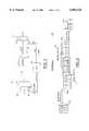
- the Ethernet repeater 10generally comprises a number of inputs 12a-12n that may be presented to a multiplexer 14. Each of the inputs 12a-12n may operate at a unique time base.
- the multiplexer 14presents a signal at an output 16 to a shared bus 15a coupled by a buffer 40 which may facilitate re-timing of the signals received at the inputs 12a-12n.
- a shared bus 15bmay be coupled to the buffer 40 and may present a signal to an input 18 of a demultiplexer circuit 20. The signal received at the input 18 is then presented to a number of outputs 22a-22n.
- an additional transmit bus TX -- BUS 26 and an additional received bus RX -- BUS 28,may be provided.
- the DTE port 24may be a dedicated port for connecting a workstation directly to the Ethernet repeater 10 to allow direct control. This direct connection may be in contrast to a workstation that is connected to the hub through the shared bus 15a and 15b. Since the DTE port 24 may be connected directly to the Ethernet repeater 10, a separate time domain is generally required. The time domain for the first read pointer is generally equal to the fundamental clock of the Ethernet (e.g., in the case of 100 baseT, a 25 MHZ clock). The time base for the DTE port 24 may be a function of the frequency of oscillation of the workstation connected to the DTE port 24.
- the addition of the transmit bus 26 and the receive bus 28generally requires that the same signal that is presented at the output 16 also be presented to an input 30 of the block 20 via a bus 31.
- the signal received at the input 30may be presented to the transmit bus 26 through an output 32.
- the rate of data transmission on the transmit bus 26may be a different rate than the rate of data transmission of the signal received at the input 18.
- the buffer 40may be presented having an output 42 and an output 44.
- the buffer 40may be implemented as a circular buffer such as a FIFO buffer.
- the output 42 and the output 44may present a data stream that, while relatively similar, may be received by a device having a different speed clock (or time base).
- the buffer 40In a data transmission environment, such as the Ethernet repeater 10, it is generally not convenient (or practical) to merely stop the input data stream or the output data stream. As a result, the buffer 40 generally has slightly different design criteria than a typical buffer. The status flags in the buffer 40 may indicate that data being read is invalid and may require recovery by another layer of the Ethernet protocol.
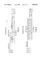
- the buffer 40generally comprises a number of memory cells 102a-102y.
- a waveform 104generally represents an incoming data stream presented to the buffer 40 while a waveform 106 generally illustrates a waveform read from the buffer 40.
- Information received from the waveform 104is written to particular memory cells 102a-102y as determined by the position of a write pointer 108.
- the write pointer 108is shown pointing to the memory location 102s.
- a read pointer 110generally follows the write pointer 108 and presents data to the output data stream 106.
- the data stored in the memory cellse.g., 102h-102r shaded in FIG.
- the write pointeris shown located at the memory cell 102s while the read pointer is shown located at the memory cell 102h.
- valid buffer datamay be stored in the memory cells 102h-102r.
- the memory cells 102a-102g and the memory cells 102s-102ygenerally have data that has already been read since the read pointer 110 has already passed. This may allow the write pointer 108 to allow the overwriting of the previously read (and now invalid) data.
- the buffer 40is shown illustrating an overflow condition.
- An overflow conditionmay occur when the write pointer 108 circles back from the last memory cell, in this case 102y, back to the first memory cell, in this case 102a, and then catches up to the read pointer 110.
- the write pointer 108is shown located at the memory cell 102k while the read pointer 110 is shown located at the memory cell 102L. If the next write occurs before the next read occurs, data may be written to the memory cell 102L before the previously written data has been read. This condition of overwriting otherwise valid data is called an overflow condition, and is generally undesirable in a circular buffer since otherwise valid data may be lost when written over.
- the buffer 40is shown illustrating an underflow condition.
- the read pointer 110is shown having only a single piece of information to be read from the memory cell 102L.
- the write pointer 108has not yet allowed information to be written to the memory cell 102m.
- An underflow conditionmust generally be accommodated for by a status flag or other device which may disable the progression of the read pointer 110 for an amount of time necessary to allow the write pointer 108 to advance or "catch up", or may indicate that the data presented from the buffer 40 is not valid.
- the status flags associated with underflow and overflow conditionsmay be implemented in a variety of ways. For example, see U.S. Pat. No. 5,627,979, the appropriate sections which are hereby incorporated by reference.
- the Ethernet repeater 10 shown in FIG. 1may require a single buffer 40 having multiple read pointers.
- independent overrun/underrun detection circuitsmay be necessary for each of the read pointers.
- the complexity of the overrun detection circuitrymust be kept to a minimum in order to ensure that the overall die area consumed by the buffer 40 and overrun detection circuitry does not interfere with the implementation the Ethernet repeater 10.
- the buffer or FIFO 40is shown implementing a write pointer 150, a read pointer 152 (e.g., Read -- Pointer -- 3), a read pointer 154 (e.g., Read -- Pointer -- 1), a read pointer 156 (e.g., Read -- Pointer -- 2), and a number of memory cells 158a-158y.
- the particular number of memory cells 158a-158y implementedmay be adjusted accordingly to meet the design criteria of a particular application.
- the write pointer 150generally indicates a portion of the memory cells 158a-158y for which data received from an input data stream 160 may be written.
- the read pointer 152generally indicates a portion of the memory cells 158a-158y for which an output waveform 162 may be read.
- the read pointer 154generally indicates a portion of the memory cells 158a-158y for which an output waveform 164 may be read.
- the read pointer 156has a similar operation to the read pointers 152 and 154 in that it indicates a particular portion of the memory cells 158-158y for which an output waveform 166 may be read.
- the FIFO 40also comprises a number of overrun detection circuits 170a-170n.
- the overrun detection circuit 170ahas an input 172a that may receive the write pointer 150 and an input 174a that may receive the read pointer 152.
- the overrun detection circuit 170agenerally comprises an output 176a that may present a signal, such as a status flag, that indicates when an overflow condition between the write pointer 150 and the read pointer 152 occurs.
- the output 178agenerally provides a signal, such as a flag, that indicates when an underflow condition occurs between the write pointer 150 and the read pointer 152.
- the overrun detection circuits 170b through 170nprovide similar inputs and outputs.
- the overrun detection circuit 170bhas an input 172b that may receive the write pointer 150, an input 174b that may receive the read pointer 154, an output 176b that may present a signal, such as a flag, when an overflow condition occurs between the write pointer 150 and the read pointer 154, and an output 178b that may present an output flag signal when an underflow condition occurs between the write pointer 150 and the read pointer 154.
- the overrun detection circuit 170nhas an input 172n that may receive the write pointer 150 and an input 174n that may receive the read pointer 156.
- the outputs 176n and 178nmay provide signals during an overflow and underflow condition between the write pointer 150 and the read pointer 156.
- the FIFO buffer 40generally provides the output data streams 162, 164, and 166 derived from a single input data stream 160 while using a single set of memory cells (or storage elements) 158a-158y. As a result, a multiple number of independently timed outputs may be generated.
- Each of the read pointers 152, 154, and 156may be tracked with a respect to the common write pointer 150 to detect overrun conditions for that particular output stream.
- the output having the fastest transmit clockwill determine which of the read pointers may reach the underflow condition, while the output having the slowest transmit clock will determine which of the read pointers may reach the overflow condition.
- the read pointers 152, 154, and 156are related in the sense that (i) each of the pointers generally follows the overflow and underflow constraints and (ii) all of the pointers, as a collective group, generally follows the overflow and underflow constraints generally allowing each of the transmit streams to remain valid.
- FIG. 6a more detailed diagram of one of the overrun detection circuits 170a-170n is shown comprising a write address logic block (or circuit) 182, a data buffer 184, a read address logic block (or circuit) 186, a compare block (or circuit) 188, a phase shift sign block (or circuit) 190, a gate 192 and a gate 194.
- the data buffer 184comprises an input 200 for receiving an input signal (e.g., write data), an input 202 which may receive the write pointer signal 150, an input 204 which may receive one of the read pointer signals 152 (or 154 or 156 of FIG. 5) and an output 206 which may present a read data output.
- the write address logic block 182generally comprises an input 208 that may receive an externally generated write clock.
- the write address logic 182 and the read address logic 186generally present the write pointer 150 and the read pointer 152 (or 154 or 156) that sequentially progress through each of the storage elements 158a-158y in a non-repetitive pattern.
- the non-repetitive patternmay be implemented as a sequence that skips certain memory cells 158a-158y.
- the sequential progressionmay, in one example, progress from memory cell 158d, to 158k to 158t, etc., such that each of the memory cells 158a-158y are addressed prior to the repeating of the sequential pattern.
- the circuit of FIG. 5shows the additional nomenclature for the memory cells as a-y, which generally accounts for the progression through the memory cells 158a-158y.
- the memory cell amay not be physically located next to the memory cell b.
- FIG. 5shows the locations of the memory cells as being adjacent.
- One such examplemay include the ability to dynamically adjust the size of the buffer according to certain design constraints.
- Another examplemay involve the production of a single buffer to be used in a variety of design applications where one or more small buffers may be implemented from a larger buffer.
- Another examplemay include the elimination of memory cells that do not pass a post-production test from the progression.
- the write address logic 182generally comprises an output 210 that generally presents the write pointer to the input 202 of the data buffer 184 as well as to an input 212 of the compare circuit 188.
- the sequential progression of the read pointer 152 (or 154 or 156) and the write pointer 150 through the storage elements 158a-158ymay be represented as a progression of binary values.
- TABLE 1illustrates such a progression using a five bit counter to progress through twenty four memory cells 158a-158x. However, other counters may be used to present other combinations required for particular design considerations.
- TABLE 1specifies a gray code counting sequence implemented in a preferred embodiment of the write address logic 182 and the read address logic 186.
- the gray code sequencemay be implemented such that only a single bit of the five bits changes during the progression between two adjacent numbers.
- the first row labeled 4, 3, 2, 1, and 0provides the particular bit of the write pointer 150 or read pointer 152 (or 154 or 156).
- the bit 0generally represents the sequence for the signal ReadPointer[0] and the signal WritePointer[0].
- the implementation of a gray code sequencemay reduce the tendency of a glitch condition to occur. However, certain other sequences may be used accordingly to meet the design criteria of a particular application.
- filteringmay be provided at the output of the phase shift sign circuit 190 to compensate for any glitches that may occur.
- a semi-gray sequencemay be used where portions of the sequence are implemented as a gray code sequence, while other portions demonstrate transitions where more than one bit change occurs during a particular transition.
- Such a semi-gray code sequencemay be used where certain known transitions are known to not cause a glitch condition, or may only a cause a minor glitch which may be accommodated by minor filtering.
- the read address logic 186generally comprises an input 216 for receiving an externally generated read clock and an output 218 for presenting the read pointer signal to the input 204 of the data buffer 184 as well as to an input 220 of the compare circuit 188.
- a single bit of the read pointermay be presented to an input 222 of the phase shift sign circuit 190.
- the phase shift sign circuit 190may be implemented as a state machine to be described in more detail in connection with FIG. 7.
- An input 224 of the phase shift sign circuit 190generally receives the externally generated read clock.
- the phase shift sign circuit 190also has an output 226 that presents a signal to both the gate 192 and the gate 194.
- An output 228 of the compare block 188presents a signal to both the gate 192 and the gate 194.
- the signal presented at the output 226 of the circuit 190is generally presented to an inverted input of the gate 192.
- the gate 192presents a signal indicating an underflow condition
- the gate 194presents a signal indicating
- the overrun detection circuit 170generally operates by recognizing the difference between an "almost empty” and “almost full” condition, without the reliance on specifically counting the number of pulses of the data input and the data output.
- the phase relationship between the write data presented at the input 200 and data received from the output 206changes over time.
- a signal representing the sign of this changemay be developed, which dynamically indicates which overrun condition is approaching.
- a simple equivalence comparison of the read and write addresses expressed and implemented in gray codecan be used to trigger an overrun condition. A more detailed description of the particular sign history of the detection circuit will be described in connection with FIG. 7.
- the phase shift sign computationis generally implemented as a four-state logic.
- the circuit 190is synchronously clocked by the read data clock.
- the inputs 214 and 222may be received directly from the least significant bit (LSB) of the gray code counters (e.g., the write address logic 182 and the read address logic 184) used for data buffer addressing.
- a signal WritePointer[0] received at the input 214may be re-timed to the read data clock.
- a signal ReadPointer[0]may be received at the input 222.
- the gray code address sequenceimposes a divide by four functionality on the gray code (LSBs). As a result, the sampling clock (the read clock in this particular example) will generally not miss a transition of the phase detector inputs.
- the write clock, an external reference clock, or other appropriate clockmay be used to synchronize the overrun detection circuit 170.
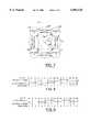
- a state machine 191is shown implementing the logic of the phase shift sign block 190.
- the state machine 191tracks a changing phase in relationship of the signal WritePointer[0] with respect to the signal ReadPointer[0].
- the output of the phase shift sign block 190determines the direction in which the state machine 191 is traversing the particular states.
- the state logicacts as a phase detector, responding to a transition on either input. The input transitions determine the particular order of the state transitions, which in turn determines the direction.
- the state machine 191generally comprises a phase45 state 252, a phase135 state 254, a phase225 state 256 and a phase315 state 258.
- the state 252may also be represented by the binary reference 11
- the state 254may also be represented by the binary reference 01
- the state 256may also be represented by the binary reference 00
- the state 258may also be represented by the binary reference 10.
- the state machine 191generally represents a configuration such that any particular state 252-258 may progress to any other particular state 252-258 in a generally direct fashion.
- the state 252has an exit 260 allowing progression to the state 254 as well as an entry 262 to return from the state 254.
- an exit 264 and a corresponding entry 266connect the state 252 to the state 258.
- An entry/exit 270allows the progression between the state 120 and state 124.
- the states 122, 124 and 126have similar configurations with the remaining states.
- FIGS. 8 and 9two input sequences are shown that illustrate the detection of the sign of the output 226 presented by the state machine 190.
- values for stateare expressed in binary, while values for the direction are expressed as a scalar.
- FIG. 8illustrates the state and direction progression for the case where the signal ReadPointer[0] has a frequency less than that of the signal WritePointer[0].
- FIG. 9illustrates the state and direction progression for the case where the signal ReadPointer[0] has a frequency greater than that of the signal WritePointer[0].
- FIG. 10The syntax of FIG. 10 is understood to be an example of verilog hardware description language (HDL) as defined by the IEEE 1364-1995 standard. While the code illustrated in FIG. 10 explicitly defines certain conditions, other implementations, including, but not limited to, discrete logic components, may be implemented to meet the design criteria of a particular application.
- HDLverilog hardware description language
- the "case(state)" constructcauses evaluation to pass to the section representing the current state of the circuit 190.
- the code evaluationstarts at the label "PHASE315:” and the other sections are ignored.
- the else/if constructis evaluated sequentially using current values of state, and inputs.
- the first true conditional associated parenthetically to an "if(. . . )” or "else if(. . . )”causes the procedure immediately following to be executed. If none of the conditionals is true, the procedure following the "else” construct is executed.
- a procedureis generally defined as a sequence of value assignments enclosed in a begin/end pair.
- the evaluationpasses back to the "case(state)" for re-evaluation with updated state and input values.
- the "! symbolmeans negation in the logical sense.
- ”mean logical AND and logical OR, respectively.
- "1'b0”is an example of a one bit binary constant having a logic 0 value.
- the operator " ⁇ "means logical EXCLUSIVE NOR of the operands.
Landscapes
- Engineering & Computer Science (AREA)
- Computer Networks & Wireless Communication (AREA)
- Signal Processing (AREA)
- Data Exchanges In Wide-Area Networks (AREA)
Abstract
Description
TABLE 1 ______________________________________ 4 3 2 1 0 ______________________________________ a 0 0 0 0 0b 0 0 0 0 1c 0 0 0 1 1d 0 0 0 1 0e 0 0 1 1 0f 0 0 1 1 1g 0 0 1 0 1h 0 0 1 0 0i 0 1 1 0 0j 0 1 1 0 1k 0 1 1 1 1l 0 1 1 1 0m 1 1 1 1 0n 1 1 1 1 1o 1 1 1 0 1p 1 1 1 0 0q 1 0 1 0 0r 1 0 1 0 1s 1 0 1 1 1t 1 0 1 1 0u 1 0 0 1 0v 1 0 0 1 1w 1 0 0 0 1 x 1 0 0 0 0 ______________________________________
Claims (15)
Priority Applications (1)
| Application Number | Priority Date | Filing Date | Title |
|---|---|---|---|
| US08/919,999US6092128A (en) | 1997-08-28 | 1997-08-28 | Ethernet repeater that couples an input data stream to multiple output data streams of differing rates and provides access to a shared bus by a number of inputs and outputs |
Applications Claiming Priority (1)
| Application Number | Priority Date | Filing Date | Title |
|---|---|---|---|
| US08/919,999US6092128A (en) | 1997-08-28 | 1997-08-28 | Ethernet repeater that couples an input data stream to multiple output data streams of differing rates and provides access to a shared bus by a number of inputs and outputs |
Publications (1)
| Publication Number | Publication Date |
|---|---|
| US6092128Atrue US6092128A (en) | 2000-07-18 |
Family
ID=25442997
Family Applications (1)
| Application Number | Title | Priority Date | Filing Date |
|---|---|---|---|
| US08/919,999Expired - LifetimeUS6092128A (en) | 1997-08-28 | 1997-08-28 | Ethernet repeater that couples an input data stream to multiple output data streams of differing rates and provides access to a shared bus by a number of inputs and outputs |
Country Status (1)
| Country | Link |
|---|---|
| US (1) | US6092128A (en) |
Cited By (17)
| Publication number | Priority date | Publication date | Assignee | Title |
|---|---|---|---|---|
| US6407742B1 (en)* | 1999-04-09 | 2002-06-18 | Ati International Srl | Method and apparatus for combining multiple line elements to produce resultant line data |
| US6463069B1 (en)* | 1996-06-25 | 2002-10-08 | Telefonaktiebolaget Lm Ericsson | Arrangement and method relating to a telecommunications system handling redundant signals |
| US20020188775A1 (en)* | 2001-06-07 | 2002-12-12 | Victor Konrad | Method and apparatus for utilizing static queues in processor staging |
| US20030037190A1 (en)* | 2001-05-10 | 2003-02-20 | Thomas Alexander | Flexible FIFO system for interfacing between datapaths of variable length |
| US6687255B1 (en)* | 2000-03-21 | 2004-02-03 | Lsi Logic Corporation | Data communication circuit having FIFO buffer with frame-in-FIFO generator |
| US20040136373A1 (en)* | 2003-01-13 | 2004-07-15 | Bareis Bernard F. | Broadband multi-drop local network, interface and method for multimedia access |
| US6766388B2 (en) | 2001-07-27 | 2004-07-20 | International Business Machines Corporation | Method for determining a host data transfer goal in a hard disk drive system |
| US6785752B2 (en) | 2001-03-23 | 2004-08-31 | International Business Machines Corporation | Method for dynamically adjusting buffer utilization ratios in a hard disk drive system |
| US20040243743A1 (en)* | 2003-05-30 | 2004-12-02 | Brian Smith | History FIFO with bypass |
| US20050005274A1 (en)* | 2000-07-31 | 2005-01-06 | Microsoft Corporation | Flexible interface for controlling streaming data in passive streaming plug-ins |
| US20050013395A1 (en)* | 2003-07-15 | 2005-01-20 | Adtran, Inc. | Data buffer-controlled digital clock regenerator |
| US20060104314A1 (en)* | 2004-10-15 | 2006-05-18 | Kddi Corporation | Audio playback apparatus for controlling pause and resume of audio |
| US20070112820A1 (en)* | 2002-06-28 | 2007-05-17 | Witt Wesley A | Transporting Image Files |
| US20080016304A1 (en)* | 2002-06-28 | 2008-01-17 | Microsoft Corporation | Method and System For Creating and Restoring An Image File |
| US7444593B1 (en)* | 2000-10-04 | 2008-10-28 | Apple Inc. | Disk space management and clip remainder during edit operations |
| US20140149694A1 (en)* | 2012-11-27 | 2014-05-29 | Donghan Lee | System-on-chip and application processor including fifo buffer and mobile device comprising the same |
| US20140237473A1 (en)* | 2009-02-27 | 2014-08-21 | International Business Machines Corporation | Virtualization of storage buffers used by asynchronous processes |
Citations (11)
| Publication number | Priority date | Publication date | Assignee | Title |
|---|---|---|---|---|
| US5084841A (en)* | 1989-08-14 | 1992-01-28 | Texas Instruments Incorporated | Programmable status flag generator FIFO using gray code |
| US5339418A (en)* | 1989-06-29 | 1994-08-16 | Digital Equipment Corporation | Message passing method |
| US5349683A (en)* | 1992-07-16 | 1994-09-20 | Mosel-Vitelic | Bidirectional FIFO with parity generator/checker |
| US5384744A (en)* | 1992-11-23 | 1995-01-24 | Paradigm Technology, Inc. | Look ahead flag for FIFO |
| US5414455A (en)* | 1993-07-07 | 1995-05-09 | Digital Equipment Corporation | Segmented video on demand system |
| US5426756A (en)* | 1992-08-11 | 1995-06-20 | S3, Incorporated | Memory controller and method determining empty/full status of a FIFO memory using gray code counters |
| US5555524A (en)* | 1995-02-13 | 1996-09-10 | Standard Microsystems Corporation | Semi-synchronous dual port FIFO |
| US5594702A (en)* | 1995-06-28 | 1997-01-14 | National Semiconductor Corporation | Multi-first-in-first-out memory circuit |
| US5627797A (en)* | 1995-12-14 | 1997-05-06 | Cypress Semiconductor Corporation | Full and empty flag generator for synchronous FIFOS |
| US5765187A (en)* | 1991-04-05 | 1998-06-09 | Fujitsu Limited | Control system for a ring buffer which prevents overrunning and underrunning |
| US5809557A (en)* | 1996-01-31 | 1998-09-15 | Galileo Technologies Ltd. | Memory array comprised of multiple FIFO devices |
- 1997
- 1997-08-28USUS08/919,999patent/US6092128A/ennot_activeExpired - Lifetime
Patent Citations (11)
| Publication number | Priority date | Publication date | Assignee | Title |
|---|---|---|---|---|
| US5339418A (en)* | 1989-06-29 | 1994-08-16 | Digital Equipment Corporation | Message passing method |
| US5084841A (en)* | 1989-08-14 | 1992-01-28 | Texas Instruments Incorporated | Programmable status flag generator FIFO using gray code |
| US5765187A (en)* | 1991-04-05 | 1998-06-09 | Fujitsu Limited | Control system for a ring buffer which prevents overrunning and underrunning |
| US5349683A (en)* | 1992-07-16 | 1994-09-20 | Mosel-Vitelic | Bidirectional FIFO with parity generator/checker |
| US5426756A (en)* | 1992-08-11 | 1995-06-20 | S3, Incorporated | Memory controller and method determining empty/full status of a FIFO memory using gray code counters |
| US5384744A (en)* | 1992-11-23 | 1995-01-24 | Paradigm Technology, Inc. | Look ahead flag for FIFO |
| US5414455A (en)* | 1993-07-07 | 1995-05-09 | Digital Equipment Corporation | Segmented video on demand system |
| US5555524A (en)* | 1995-02-13 | 1996-09-10 | Standard Microsystems Corporation | Semi-synchronous dual port FIFO |
| US5594702A (en)* | 1995-06-28 | 1997-01-14 | National Semiconductor Corporation | Multi-first-in-first-out memory circuit |
| US5627797A (en)* | 1995-12-14 | 1997-05-06 | Cypress Semiconductor Corporation | Full and empty flag generator for synchronous FIFOS |
| US5809557A (en)* | 1996-01-31 | 1998-09-15 | Galileo Technologies Ltd. | Memory array comprised of multiple FIFO devices |
Non-Patent Citations (3)
| Title |
|---|
| Cypress CY7C408A, CY7C409A, 64 x 8 Cascadable FIFO, 64 x 9 Cascadable FIFO, Jul. 1994, pp. 1 16.* |
| Cypress CY7C408A, CY7C409A, 64 x 8 Cascadable FIFO, 64 x 9 Cascadable FIFO, Jul. 1994, pp. 1-16. |
| Michael F. Maas, U.S.S.N. 08/919,653 Circuit(s) Method(s) and Architecture for Providing Multiple Data Output Streams from a Data Input Stream, filed Aug. 28, 1997.* |
Cited By (35)
| Publication number | Priority date | Publication date | Assignee | Title |
|---|---|---|---|---|
| US6463069B1 (en)* | 1996-06-25 | 2002-10-08 | Telefonaktiebolaget Lm Ericsson | Arrangement and method relating to a telecommunications system handling redundant signals |
| US6407742B1 (en)* | 1999-04-09 | 2002-06-18 | Ati International Srl | Method and apparatus for combining multiple line elements to produce resultant line data |
| US6687255B1 (en)* | 2000-03-21 | 2004-02-03 | Lsi Logic Corporation | Data communication circuit having FIFO buffer with frame-in-FIFO generator |
| US6934954B1 (en)* | 2000-07-31 | 2005-08-23 | Microsoft Corporation | Flexible interface for controlling streaming data in passive streaming plug-ins |
| US20050005274A1 (en)* | 2000-07-31 | 2005-01-06 | Microsoft Corporation | Flexible interface for controlling streaming data in passive streaming plug-ins |
| US7600233B2 (en)* | 2000-07-31 | 2009-10-06 | Microsoft Corporation | Flexible interface for controlling streaming data in passive streaming plug-ins |
| US7444593B1 (en)* | 2000-10-04 | 2008-10-28 | Apple Inc. | Disk space management and clip remainder during edit operations |
| US6785752B2 (en) | 2001-03-23 | 2004-08-31 | International Business Machines Corporation | Method for dynamically adjusting buffer utilization ratios in a hard disk drive system |
| US20030037190A1 (en)* | 2001-05-10 | 2003-02-20 | Thomas Alexander | Flexible FIFO system for interfacing between datapaths of variable length |
| US6754741B2 (en)* | 2001-05-10 | 2004-06-22 | Pmc-Sierra, Inc. | Flexible FIFO system for interfacing between datapaths of variable length |
| US6633972B2 (en)* | 2001-06-07 | 2003-10-14 | Intel Corporation | Method and apparatus for utilizing static queues in processor staging |
| US20020188775A1 (en)* | 2001-06-07 | 2002-12-12 | Victor Konrad | Method and apparatus for utilizing static queues in processor staging |
| US6766388B2 (en) | 2001-07-27 | 2004-07-20 | International Business Machines Corporation | Method for determining a host data transfer goal in a hard disk drive system |
| US20080016304A1 (en)* | 2002-06-28 | 2008-01-17 | Microsoft Corporation | Method and System For Creating and Restoring An Image File |
| US20070112820A1 (en)* | 2002-06-28 | 2007-05-17 | Witt Wesley A | Transporting Image Files |
| US7818532B2 (en) | 2002-06-28 | 2010-10-19 | Microsoft Corporation | Method and system for creating and restoring an image file |
| EP1376404A3 (en)* | 2002-06-28 | 2008-02-06 | Microsoft Corporation | Method and system for managing backup files |
| US7877567B2 (en) | 2002-06-28 | 2011-01-25 | Microsoft Corporation | Transporting image files |
| US8300654B2 (en) | 2003-01-13 | 2012-10-30 | Bareis Bernard F | Broadband multi-drop local network, interface and method for multimedia access |
| US8837514B2 (en) | 2003-01-13 | 2014-09-16 | Bernard F. Bareis | Broadband multi-drop local network, interface and method for multimedia access |
| US7346071B2 (en) | 2003-01-13 | 2008-03-18 | Bareis Bernard F | Broadband multi-drop local network, interface and method for multimedia access |
| US20080310436A1 (en)* | 2003-01-13 | 2008-12-18 | Bareis Bernard F | Broadband multi-drop local network, interface and method for multimedia access |
| US20040136373A1 (en)* | 2003-01-13 | 2004-07-15 | Bareis Bernard F. | Broadband multi-drop local network, interface and method for multimedia access |
| US7117287B2 (en)* | 2003-05-30 | 2006-10-03 | Sun Microsystems, Inc. | History FIFO with bypass wherein an order through queue is maintained irrespective of retrieval of data |
| US20040243743A1 (en)* | 2003-05-30 | 2004-12-02 | Brian Smith | History FIFO with bypass |
| US7212598B2 (en)* | 2003-07-15 | 2007-05-01 | Adtran, Inc. | Data buffer-controlled digital clock regenerator |
| US20050013395A1 (en)* | 2003-07-15 | 2005-01-20 | Adtran, Inc. | Data buffer-controlled digital clock regenerator |
| US7650422B2 (en)* | 2004-10-15 | 2010-01-19 | Kddi Corporation | Audio playback apparatus for controlling pause and resume of audio |
| US20060104314A1 (en)* | 2004-10-15 | 2006-05-18 | Kddi Corporation | Audio playback apparatus for controlling pause and resume of audio |
| US20140237473A1 (en)* | 2009-02-27 | 2014-08-21 | International Business Machines Corporation | Virtualization of storage buffers used by asynchronous processes |
| US10268499B2 (en)* | 2009-02-27 | 2019-04-23 | International Business Machines Corporation | Virtualization of storage buffers used by asynchronous processes |
| US10613895B2 (en) | 2009-02-27 | 2020-04-07 | International Business Machines Corporation | Virtualization of storage buffers used by asynchronous processes |
| US20140149694A1 (en)* | 2012-11-27 | 2014-05-29 | Donghan Lee | System-on-chip and application processor including fifo buffer and mobile device comprising the same |
| KR20140067740A (en)* | 2012-11-27 | 2014-06-05 | 삼성전자주식회사 | System-on-chip and application processor including fifo buffer and mobile device comprising the same |
| US9542152B2 (en)* | 2012-11-27 | 2017-01-10 | Samsung Electronics Co., Ltd. | System-on-chip and application processor including FIFO buffer and mobile device comprising the same |
Similar Documents
| Publication | Publication Date | Title |
|---|---|---|
| US5978868A (en) | System for generating buffer status flags by comparing read and write pointers and determining direction of progression of read pointer with respect to write pointer | |
| US6092128A (en) | Ethernet repeater that couples an input data stream to multiple output data streams of differing rates and provides access to a shared bus by a number of inputs and outputs | |
| US7310396B1 (en) | Asynchronous FIFO buffer for synchronizing data transfers between clock domains | |
| US6718449B2 (en) | System for data transfer between different clock domains, and for obtaining status of memory device during transfer | |
| EP1124179B1 (en) | An apparatus for signal synchronization between two clock domains | |
| US5524270A (en) | System for transferring data between asynchronous data buses with a data buffer interposed in between the buses for synchronization of devices timed by different clocks | |
| US6594329B1 (en) | Elastic buffer | |
| US5587953A (en) | First-in-first-out buffer memory | |
| US6101329A (en) | System for comparing counter blocks and flag registers to determine whether FIFO buffer can send or receive data | |
| US7072349B2 (en) | Ethernet device and method for extending ethernet FIFO buffer | |
| US6687255B1 (en) | Data communication circuit having FIFO buffer with frame-in-FIFO generator | |
| US6154796A (en) | Apparatus and method in a network interface device for storing receiving frame status in a holding register | |
| EP0226017A2 (en) | Data synchronizer between a source system and a sink system | |
| US7107393B1 (en) | Systems and method for transferring data asynchronously between clock domains | |
| JPH03238686A (en) | Method and device for generating state flag | |
| TWI400917B (en) | Data processing systems and methods | |
| EP1402340B1 (en) | First-in, first-out memory system and method thereof | |
| US5222108A (en) | Cell transmission phase and rate converting circuit capable of minimizing extension of faults | |
| US6061768A (en) | Apparatus and method in a network interface device for storing tracking information indicating stored data status between contending memory controllers | |
| EP0217486B1 (en) | A synchronizing system | |
| US6473818B1 (en) | Apparatus and method in a network interface device for asynchronously generating SRAM full and empty flags using coded read and write pointer values | |
| EP0695988A2 (en) | A first-in first-out memory | |
| US20030005344A1 (en) | Synchronizing data with a capture pulse and synchronizer | |
| US7136309B2 (en) | FIFO with multiple data inputs and method thereof | |
| US6098139A (en) | Frequency independent asynchronous clock crossing FIFO |
Legal Events
| Date | Code | Title | Description |
|---|---|---|---|
| AS | Assignment | Owner name:CYPRESS SEMICONDUCTOR CORPORATION, CALIFORNIA Free format text:ASSIGNMENT OF ASSIGNORS INTEREST;ASSIGNORS:MAAS, MICHAEL F.;SOMER, GREGORY B.;REEL/FRAME:008825/0748;SIGNING DATES FROM 19970827 TO 19971111 | |
| STCF | Information on status: patent grant | Free format text:PATENTED CASE | |
| FPAY | Fee payment | Year of fee payment:4 | |
| FPAY | Fee payment | Year of fee payment:8 | |
| REMI | Maintenance fee reminder mailed | ||
| FPAY | Fee payment | Year of fee payment:12 | |
| AS | Assignment | Owner name:HAUGH TELECOM LLC, DELAWARE Free format text:ASSIGNMENT OF ASSIGNORS INTEREST;ASSIGNOR:CYPRESS SEMICONDUCTOR CORPORATION;REEL/FRAME:029651/0890 Effective date:20121213 | |
| AS | Assignment | Owner name:NYTELL SOFTWARE LLC, DELAWARE Free format text:MERGER;ASSIGNOR:HAUGH TELECOM LLC;REEL/FRAME:037392/0358 Effective date:20150826 | |
| AS | Assignment | Owner name:HANGER SOLUTIONS, LLC, GEORGIA Free format text:ASSIGNMENT OF ASSIGNORS INTEREST;ASSIGNOR:INTELLECTUAL VENTURES ASSETS 158 LLC;REEL/FRAME:051486/0425 Effective date:20191206 | |
| AS | Assignment | Owner name:INTELLECTUAL VENTURES ASSETS 158 LLC, DELAWARE Free format text:ASSIGNMENT OF ASSIGNORS INTEREST;ASSIGNOR:NYTELL SOFTWARE LLC;REEL/FRAME:051777/0173 Effective date:20191126 |