US6091473A - Active matrix liquid crystal display - Google Patents
Active matrix liquid crystal displayDownload PDFInfo
- Publication number
- US6091473A US6091473AUS09/082,705US8270598AUS6091473AUS 6091473 AUS6091473 AUS 6091473AUS 8270598 AUS8270598 AUS 8270598AUS 6091473 AUS6091473 AUS 6091473A
- Authority
- US
- United States
- Prior art keywords
- common electrode
- liquid crystal
- gate wiring
- pixel electrode
- wiring
- Prior art date
- Legal status (The legal status is an assumption and is not a legal conclusion. Google has not performed a legal analysis and makes no representation as to the accuracy of the status listed.)
- Expired - Lifetime
Links
Images


Classifications
- G—PHYSICS
- G02—OPTICS
- G02F—OPTICAL DEVICES OR ARRANGEMENTS FOR THE CONTROL OF LIGHT BY MODIFICATION OF THE OPTICAL PROPERTIES OF THE MEDIA OF THE ELEMENTS INVOLVED THEREIN; NON-LINEAR OPTICS; FREQUENCY-CHANGING OF LIGHT; OPTICAL LOGIC ELEMENTS; OPTICAL ANALOGUE/DIGITAL CONVERTERS
- G02F1/00—Devices or arrangements for the control of the intensity, colour, phase, polarisation or direction of light arriving from an independent light source, e.g. switching, gating or modulating; Non-linear optics
- G02F1/01—Devices or arrangements for the control of the intensity, colour, phase, polarisation or direction of light arriving from an independent light source, e.g. switching, gating or modulating; Non-linear optics for the control of the intensity, phase, polarisation or colour
- G02F1/13—Devices or arrangements for the control of the intensity, colour, phase, polarisation or direction of light arriving from an independent light source, e.g. switching, gating or modulating; Non-linear optics for the control of the intensity, phase, polarisation or colour based on liquid crystals, e.g. single liquid crystal display cells
- G02F1/133—Constructional arrangements; Operation of liquid crystal cells; Circuit arrangements
- G02F1/1333—Constructional arrangements; Manufacturing methods
- G02F1/1343—Electrodes
- G02F1/134309—Electrodes characterised by their geometrical arrangement
- G02F1/134363—Electrodes characterised by their geometrical arrangement for applying an electric field parallel to the substrate, i.e. in-plane switching [IPS]
- G—PHYSICS
- G02—OPTICS
- G02F—OPTICAL DEVICES OR ARRANGEMENTS FOR THE CONTROL OF LIGHT BY MODIFICATION OF THE OPTICAL PROPERTIES OF THE MEDIA OF THE ELEMENTS INVOLVED THEREIN; NON-LINEAR OPTICS; FREQUENCY-CHANGING OF LIGHT; OPTICAL LOGIC ELEMENTS; OPTICAL ANALOGUE/DIGITAL CONVERTERS
- G02F1/00—Devices or arrangements for the control of the intensity, colour, phase, polarisation or direction of light arriving from an independent light source, e.g. switching, gating or modulating; Non-linear optics
- G02F1/01—Devices or arrangements for the control of the intensity, colour, phase, polarisation or direction of light arriving from an independent light source, e.g. switching, gating or modulating; Non-linear optics for the control of the intensity, phase, polarisation or colour
- G02F1/13—Devices or arrangements for the control of the intensity, colour, phase, polarisation or direction of light arriving from an independent light source, e.g. switching, gating or modulating; Non-linear optics for the control of the intensity, phase, polarisation or colour based on liquid crystals, e.g. single liquid crystal display cells
- G02F1/133—Constructional arrangements; Operation of liquid crystal cells; Circuit arrangements
- G02F1/136—Liquid crystal cells structurally associated with a semi-conducting layer or substrate, e.g. cells forming part of an integrated circuit
Definitions
- the present inventionrelates to an active matrix liquid crystal display which controls the orientation of liquid crystal by applying a lateral electric field in a direction along the surface of a substrate and particularly, relates to structure which enables the enhancement of the numerical aperture.
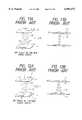
- an electrode for driving liquid crystalis not respectively provided to the upper and lower substrates which holds a liquid crystal layer between them but two types of linear electrodes 12 and 13 with different poles are provided only to the lower substrate 11 with the above electrodes mutually separated as shown in FIG. 10, no electrode is provided to the upper substrate 10 shown in FIG. 10 and liquid crystal molecules 36 can be oriented in the direction (the direction of the surface of the substrate) of a lateral electric field generated between both linear electrodes 12 and 13 by applying voltage.
- a comb-type electrode 16is constituted by connecting each linear electrode 12 to a base line part 14
- a comb-type electrode 17is constituted by connecting each linear electrode 13 to a base line part 15, both comb-type electrodes 16 and 17 are combined
- a switching element 19is connected to the base line part 14
- a power source 18is connected to the base line part 15.
- a polarizing plate provided with the polarization direction of a direction ⁇ shown in FIG. 11Ais laminated on the upper substrate 10 by forming an orientation film on the liquid crystal side of the upper substrate 10 and applying orientation processing to the orientation film so that liquid crystal molecules 36 are arranged in the direction of ⁇ , and a polarizing plate provided with the polarization direction of a direction ⁇ is laminated on the lower substrate 11 by forming an orientation film on the liquid crystal side of the lower substrate 11 and applying orientation processing to the orientation film so that liquid crystal molecules 36 are arranged in the direction of ⁇ parallel to the above direction ⁇ .
- liquid crystal molecules 36are homogeneously oriented in the same direction in the orientation direction of the orientation films as shown in FIGS. 11A and 11B in a state in which no voltage is applied between the linear electrodes 12 and 13.
- Back light which passes the lower substrate 11 in this stateis polarized in the direction of ⁇ by the polarizing plate, as the back light is transmitted in the layer of liquid crystal molecules 36 as it is and reaches the polarizing plate with a different polarization direction ⁇ of the upper substrate 10, it is interrupted by the polarizing plate and as no back light passes a liquid crystal display, the liquid crystal display is in a dark state.
- liquid crystal molecules 36are twistedly oriented as shown in FIGS. 12A and 12B.
- the polarization direction of light transmitted in the lower substrate 11 and polarized in the direction of ais converted by the twisted liquid crystal molecules 36, the light can pass through the upper substrate 10 provided with the polarizing plate with the polarization direction ⁇ different from the direction ⁇ and the liquid crystal display is in a light state.
- FIGS. 13A, 13B and 13Cshow the structure of a liquid crystal display provided with the linear electrodes 12 and 13 provided with the above structure in case the structure of the liquid crystal display is applied to an actual active matrix liquid crystal driving circuit.
- FIG. 13Ashows the planar structure of each electrode
- FIGS. 13B and 13Cshow the sectional structure
- gate wirings 21 and source wirings 22 arranged in a matrix on a substrate 20are formed on/over the transparent substrate 20 via an insulating layer 24 between them and a part equivalent to each rectangular area surrounded by the gate wirings 21 and the source wirings 22 is a pixel area.
- a gate electrode 21acomposed of a part of the gate wiring 21 is formed at the corner of each pixel area
- a semiconductor layer 26is formed on the insulating layer 24 on the gate electrode 21a and a thin film transistor T is constituted by a source electrode 27 and a drain electrode 28 on both sides of the semiconductor layer 26.
- a common wiring 30is provided next to the gate wiring 21 on the substrate 20 so that the common wiring passes each pixel area and common electrodes 31 are provided in a part equivalent to each pixel area of each common wiring 30 so that the common electrode is adjacent to the source wiring 22 located on both sides of each picture element and the ends of the common electrodes 31 are connected by a common electrode connection 32 provided along the gate wiring 21 on the end side of the common electrode 31.
- the drain electrode 28 provided to the thin film transistor Tis connected to a capacity generating electrode 33 extended on the upper side of the common electrode connection 32, the capacity generating electrode 33 is connected to a pixel electrode 34 provided in the middle of the common electrodes 31, the pixel electrode 34 is extended to the side of the common wiring 30 and is connected to a capacity generating electrode 35 formed on the common wiring 30.
- liquid crystal moleculescan be oriented according to the lateral electric field. Therefore, a light state and a dark state can be switched by controlling the orientation of liquid crystal as in the case described above, referring to FIGS. 11 and 12.
- the liquid crystal display provided with the above structurehas a problem that the numerical aperture is often small though the display has an advantage that the angle of visibility is large.
- the orientation of liquid crystal moleculesis controlled by a lateral electric field generated between the pixel electrode 34 and each common electrode 31.
- the gate wiring 21 and the common wiring 30are both directly formed on the substrate 20 as shown in FIGS. 13B and 13C and located in the same plane, fixed space d 1 is required to be left between the gate wiring 21 and the common wiring 30 to prevent a short circuit in wiring as shown in FIGS. 13A and 13B. Because the space d 1 may be probably a defective part in which the leakage of light and others are caused, the space is required to be covered with a black matrix and others and therefore, a numerical aperture as a liquid crystal display cannot be enhanced.
- the orientation of liquid crystal molecules 36is different from that of an area between the pixel electrode 34 and the common electrode 31 as shown in FIG. 10.
- an area over the common electrode 31may cause a problem such as the leakage of light
- structure that the area is covered with a black matrixis adopted and further, structure that the periphery of a part covered with a black matrix is located slightly inside the inner edge of each common electrode 31 is adopted, therefore, an area covered with a black matrix is widened and there is a problem that a numerical aperture as a liquid crystal display cannot be enhanced.
- the present inventionis made in view of the above situation and the object is to provide a liquid crystal display which enables the enhancement of the numerical aperture with a characteristic that the angle of visibility is large in constitution that liquid crystal is driven by a lateral electric field provided.
- the present inventionis characterized in that liquid crystal is arranged between a pair of substrates, plural gate wirings and plural source wirings are provided mutually perpendicularly on the opposite surface of either of the above substrates, a thin film transistor is provided in the vicinity of each intersection of the gate wiring and the source wiring, a pixel electrode driven by the thin film transistor and a common electrode for applying a lateral electric field to the above liquid crystal in a direction along the above substrate in cooperation with the pixel electrodes and forming plural pixel electrodes are provided, an insulating layer is provided between the common electrode and the above a gate wiring and an electrode part along the gate wiring of the common electrode is provided in the vicinity of the gate wiring.
- a lateral electric fieldcan be applied to liquid crystal by the common electrode and the pixel electrode respectively provided on the substrate, the orientation of liquid crystal can be controlled by applying a lateral electric field or not applying it and hereby, a light state and a dark state can be switched.
- the gate wiring and the common electrodeare provided in separate layers on the substrate via an insulating layer, the gate wiring and the common electrode can be arranged closer, compared with those in conventional type structure which is structure in the same layer and hereby, as an interval in a plan between the gate wiring and the common electrode can be reduced, a numerical aperture as a liquid crystal display can be enhanced.
- the liquid crystal display according to the present inventionmay be also constituted so that the present invention is characterized in that the gate wiring is provided on the upper side of the common electrode, the above pixel electrode is provided on the gate wiring via a second insulating layer and an electrode part along the gate wiring of the pixel electrode is overlapped with an electrode part along the gate wiring of the common electrode.
- the liquid crystal display according to the present inventionmay be also constituted so that the present invention is characterized in that the gate wiring is provided on the upper side of the common electrode, the pixel electrode is provided on the gate wiring via the second insulating layer and an electrode part along the source wiring of the pixel electrode is overlapped with an electrode part along the source wiring of the common electrode.
- the present inventionis characterized in that liquid crystal is arranged between a pair of substrates, plural gate wirings and plural source wirings are provided mutually perpendicularly on the opposite surface of either of the above substrates, a thin film transistor is provided in the vicinity of each intersection of the gate wiring and the source wiring, a pixel electrode driven by the thin film transistor and a common electrode for applying a lateral electric field to the liquid crystal in a direction along the surface of the substrate in cooperation with the pixel electrodes to form plural pixel electrodes are provided, an insulating layer is provided between the common electrode and the gate wiring and a part overlapped with the gate wiring is formed in an electrode part along the gate wiring of the common electrode.
- the part of the common electrodecan be arranged further closer to the gate wiring in a plan and as the area of the common electrode in a pixel area can be further reduced than that in the above each structure, the numerical aperture can be enhanced.
- the liquid crystal display according to the present inventioncan be constituted so that the present invention is characterized in that in the above structure, two isolating layers are provided, the pixel electrode is provided between the upper isolating layer and the lower isolating layer and a part overlapped with the gate wiring is formed in an electrode part along the gate wiring of the pixel electrode.
- the liquid crystal display according to the present inventionmay be also constituted so that two isolating layers are provided as described above, the pixel electrode is provided between the upper isolating layer and the lower isolating layer and an electrode part along the gate wiring of the pixel electrode is overlapped with an electrode part along the gate wiring of the common electrode.
- capacitycan be secured by the overlapped part and such capacity can be utilized for the improvement of the liquid crystal driving performance of the liquid crystal display as storage capacity.
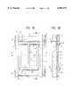
- FIGS. 1A and 1Bshow a first embodiment of a liquid crystal display according to the present invention, in which FIG. 1A is a plan showing a thin film transistor arrayed substrate and FIG. 1B is a sectional view viewed along a line 1B--1B in FIG. 1A;
- FIG. 2is a sectional view showing the main part of the liquid crystal display equivalent to the first embodiment
- FIG. 3is a sectional view viewed along a line 3--3 in FIG. 1A;
- FIGS. 4A to 4Cshow a second embodiment of the liquid crystal display according to the present invention, in which FIG. 4A is a plan showing a thin film transistor arrayed substrate, FIG. 4B is a sectional view viewed along a line 4B--4B in FIG. 4A and FIG. 4C is a sectional view viewed along a line 4C--4C in FIG. 4A;
- FIG. 5is a plan showing a third embodiment of the liquid crystal display according to the present invention.
- FIGS. 6A to 6Cshow a fourth embodiment of the liquid crystal display according to the present invention, in which FIG. 6A is a plan showing a thin film transistor arrayed substrate, FIG. 6B is a sectional view viewed along a line 6B--6B in FIG. 6A and FIG. 6C is a sectional view viewed along a line 6C--6C in FIG. 6A;
- FIG. 7is a sectional view showing a fifth embodiment of the liquid crystal display according to the present invention.
- FIGS. 8A to 8Cshow a sixth embodiment of the liquid crystal display according to the present invention, in which FIG. 8A is a plan showing a thin film transistor arrayed substrate, FIG. 8B is a sectional view viewed along a line 8B--8B in FIG. 8A and FIG. 8C is a sectional view viewed along a line 8C--8C in FIG. 8A;
- FIG. 9is a plan showing a substrate provided with linear electrodes of a liquid crystal display developed formerly and according to a method of applying a lateral electric field;
- FIG. 10is a sectional view showing the state of the orientation of liquid crystal molecules in case voltage is applied to the linear electrodes shown in FIG. 9;
- FIG. 11Ashows the orientation of liquid crystal in a dark state of the liquid crystal display developed formerly and according to the method of applying a lateral electric field and FIG. 11B is a side view of FIG. 11A;
- FIG. 12Ashows the orientation of liquid crystal in a light state of the liquid crystal display developed formerly and according to the method of applying a lateral electric field and FIG. 12B is a side view of FIG. 12A;
- FIG. 13Ashows the sectional structure in an example in which the liquid crystal display developed formerly and according to the method of applying a lateral electric field is embodied
- FIG. 13Bis a sectional view viewed along a line 13B--13B in FIG. 13A
- FIG. 13Cis a sectional view viewed along a line 13C--13C in FIG. 13A.
- FIGS. 1 to 3show a first embodiment of a liquid crystal display according to the present invention
- an upper substrate 40 and a lower substrate 41are arranged opposite in parallel at a predetermined interval (a cell gap) between the upper and lower substrates as shown in sectional structure in FIG. 2
- liquid crystal 42is provided between the substrates 40 and 41 and polarizing plates 43 and 44 are arranged on the outside surface of each substrate 40 and 41.
- These substrates 40 and 41are composed of a transparent substrate such as glass, however, in actual constitution, the periphery of each substrate 40 and 41 is surrounded by sealant, space surrounded by the substrates 40 and 41 and the sealant is filled with liquid crystal 42 and a liquid crystal cell 45 is constituted by combining the substrates 40, 41, the liquid crystal 42, the polarizing plates 43 and 44.
- plural gate wirings 50 and plural source wirings 51are formed on the transparent substrate 41 in a matrix as shown in FIG. 1A, and linear common electrodes 53 and a linear pixel electrode 54 are arranged in parallel in a pixel area 52 surrounded by the gate wirings 50 and the source wirings 51.
- plural common electrode wirings 55 for constituting a part of each common electrodeare formed on the lower substrate 41 in parallel at a predetermined interval, a first isolating layer 56 composed of SiO 2 , SiN x and others such as an insulating layer is formed with the first isolating layer covering the substrate 41 and the common electrode wirings 55, the gate wiring 50 wider than the common electrode wiring 55 is provided next to the common electrode wiring 55 on the isolating layer 56 in parallel with the common electrode wiring 55 at a minute interval of approximately 0.5 to 2.0 ⁇ m, a second isolating layer 57 such an insulating layer is formed on the first isolating layer 56 with the second isolating layer covering each gate wiring 50, and the pixel electrode 54 and the source wiring 51 are formed on the isolating layer 57.
- a first isolating layer 56composed of SiO 2 , SiN x and others such as an insulating layer is formed with the first isolating layer covering the substrate 41 and the common electrode wirings 55
- the common electrodes 53 extended from the common electrode wiring 55are formed in parallel with the source wirings 51 located on both sides of the common electrode wiring 55 for each pixel area 52 and are connected via the common electrode connection 59 provided next to the gate wiring 50 in a position close to the gate wiring 50 on the other end side (on the lower side in FIG. 1A) of each common electrode.
- a thin film transistor Tis constituted by forming a gate electrode 60 using a part of the gate wiring 50 in a part in which the gate wiring 50 and the source wiring 51 are crossed in each pixel area 52, forming a semiconductor layer 61 on the isolating layer 57 on the gate electrode 60, connecting a source electrode 62 using a part of the source wiring 51 to one side of the semiconductor layer 61 and connecting a drain electrode 63 to the other side.
- the above pixel electrode 54is arranged in parallel with the common electrodes 53 in the middle of the common electrodes 53 on both sides of each pixel area 52, a capacity generating electrode 65 over the common electrode connection 59 is formed on one side of the pixel electrode 54, the isolating layers 56 and 57 are provided between the common electrode connection 59 and the capacity generating electrode 65 so that capacity is secured and one end of the capacity generating electrode 65 is connected to the drain electrode 63.
- a capacity generating electrode 66 over the common electrode wiring 55is formed on the other side of the pixel electrode 54 in each pixel area 52 and the isolating layers 56 and 57 are provided between the common electrode wiring 55 and the capacity generating electrode so that capacity is secured.
- Capacity generated by these capacity generating electrodes 65 and 66functions as the removal of the effect of parasitic capacity when liquid crystal is driven and storage capacity for holding signal voltage.
- An orientation filmis provided on/over the isolating layer 57, the pixel electrode 54 and the source wiring 51, however, the film is omitted in sectional structure shown in FIG. 2.
- the electrodes 53 and 54 used in structure in this embodimentmay be also formed by either a shading metallic electrode or a transparent electrode. However, if a normal black type display described later is adopted, it is desirable that the electrodes are a transparent electrode composed of indium tin oxide (ITO) and others.
- ITOindium tin oxide
- a black matrix 71 provided with an opening 70 corresponding to the pixel area 52 provided on the side of the lower substrate 41is provided on the lower surface side of the upper substrate 40, each opening 70 is covered with a color filter 72 and an orientation film not shown is provided while covering the black matrix 71 and the color filter 72.
- the above black matrix 71is composed of a shading metallic film such as a chromium layer or a lamination of a chromium oxide layer and a chromium layer, covers a part which does not contribute to display of each pixel area 52 provided on the side of the lower substrate 41 and is formed so that the black matrix 71 covers a part which does not contribute to display of each pixel area 52, for example the gate wiring 50, the common electrode wiring 55, the source wiring 51, the common electrode 53, the common electrode connection 59 and the vicinity of them.
- An orientation filmis provided on the respective lower surface sides of the black matrix 71 and the color filter 72. However, the film is omitted in the sectional structure shown in FIG. 1.
- the color filter 72is provided as shown in FIG. 2 and each color of red (R), green (G) and blue (B) of the color filter is arranged every pixel area 52, however, in the case of a liquid crystal display which is not for color display, it is natural that the color filter 72 may be omitted.
- orientation processingis applied to an orientation film on the side of the upper substrate 40 and an orientation film on the side of the lower substrate 41 in an approximately parallel direction with the longitudinal direction of the common electrode 53.
- Molecules of liquid crystal 42 existing between the substrates 40 and 41are homogeneously arrayed by the above orientation processing in a state in which the longer axis of each liquid crystal molecule is directed in the longitudinal direction of the common electrode 53 (in a state in which the longer axis is directed in a direction ⁇ shown in FIG. 1A) in a state in which an electric field is not applied.
- the polarizing axis of the upper polarizing plate 43is directed in an approximately parallel direction with the longitudinal direction of the common electrode 53, and the polarizing axis of the lower polarizing plate 44 is directed in a perpendicular direction (in a lateral direction in FIG. 1A, that is, in a direction ⁇ ) to the longitudinal direction of the common electrode 53.
- a light state and a dark statecan be switched by switching whether voltage is applied between each common electrode 53 and the pixel electrode 54 in a desired pixel area 52 or not by the operation of the thin film transistor T which is a switching device.
- a lateral electric fieldcan be applied in a direction a 1 shown in FIG. 3 by applying voltage between each common electrode 53 and the pixel electrode 54 provided in a pixel area 52 in a desired position by operating the thin film transistor T. Accordingly, as in the case described referring to FIGS. 12A and 12B, liquid crystal molecules can be twisted by 90° between the upper and lower substrates to thereby obtain a light state.
- Liquid crystal moleculescan be homogeneously oriented in the same direction as the direction of the orientation film in the orientation processing in the case shown in FIGS. 11A and 11B by not applying voltage between each common electrode 53 and the pixel electrode 54, whereby a dark state can be obtained.
- the orientation of liquid crystal moleculescan be controlled and a dark state and a light state can be obtained by switching whether the light of a back light provided on the lower side of the substrate 41 is interrupted or transmitted depending upon the orientation controlled state of liquid crystal molecules.
- a state in which the orientation of liquid crystal molecules is not controlledis a dark state and a state in which the orientation of liquid crystal molecules is controlled is a light state
- a display format called normal blackis adopted as a state in which the orientation of liquid crystal molecules is not controlled is a dark state and a state in which the orientation of liquid crystal molecules is controlled is a light state.
- a display format called normal blackis adopted as the orientation of liquid crystal molecules is controlled with the molecules homogeneously oriented or twisted by 90° between both substrates 40 and 41, a liquid crystal display with a large angle of visibility in which the variation of transmissivity depending upon the angle of visibility is small can be obtained.
- the gate wiring 50 and the common electrode wiring 55are adjacent via a minute interval d 2 in a plan shown in FIG. 1A, however, as both are provided in separate layers via the isolating layer 56 such as an insulating layer, insulation performance between both is secured by the isolating layer 56 even if an interval between both is hardly made when viewed from the top or even if both are slightly overlapped to the extent that parasitic capacity does not come into question. Therefore, as shown in FIGS. 1A and 1B, the interval d 2 between the gate wiring 50 and the common electrode wiring 55 can be reduced so that the interval is smaller than the interval d 1 between the gate wiring 21 and the common electrode wiring 30 in the conventional type structure shown in FIG.
- the gate wiring 50 and the common electrode wiring 55are slightly overlapped to the extent that parasitic capacity does not come into question, the position of one side of the common electrode wiring 55 is shown by a two-dot chain line S in FIG. 1A.
- the numerical aperturecan be enhanced.
- the extent that parasitic capacity does not come into question in case the gate wiring 50 and the common electrode wiring 55 are overlappedmeans a range of approximately 0 to 3 ⁇ m.
- the above extentis not limited to the above range.
- capacitycan be secured between a capacity generating electrode 65 and the common electrode connection 59 and between a capacity generating electrode 66 and the common electrode wiring 55 by providing the capacity generating electrodes 65 and 66 and providing the common electrode wiring 55 and the common electrode connection 59 so that both are respectively opposite to the capacity generating electrodes via the isolating layers 56 and 57, and the above capacity can be utilized for the improvement of the liquid crystal driving performance of the liquid crystal capacity as storage capacity.
- FIGS. 4A to 4Cshow the main part of a liquid crystal display equivalent to a second embodiment of the present invention and as in FIGS. 4A to 4C and as the same reference numbers are allocated to the same parts as in the liquid crystal display equivalent to the first embodiment shown in FIGS. 1 to 3, the description of them is omitted.
- the liquid crystal display equivalent to this embodimentis different from the liquid crystal display equivalent to the first embodiment in that gate wirings 80 are formed on the lower substrate 41, a first isolating layer 82 such as an insulating layer is provided covering the substrate 41 and these gate wirings 80, a pixel electrode 83 and a source wiring 84 are formed on the isolating layer 82, a second isolating layer 85 such as an insulating layer is provided covering the isolating layer 82, the pixel electrode 83 and the source wiring 84, and a common electrode 86 is provided on the isolating layer 85.
- a first isolating layer 82such as an insulating layer is provided covering the substrate 41 and these gate wirings 80
- a pixel electrode 83 and a source wiring 84are formed on the isolating layer 82
- a second isolating layer 85such as an insulating layer is provided covering the isolating layer 82, the pixel electrode 83 and the source wiring 84
- two pixel electrodes 83are provided apart in parallel with the source wirings 84 in a pixel area 87 surrounded by the gate wirings 80 and the source wirings 84 as shown in FIG. 4A, each one end of the pixel electrodes 83 is connected to a capacity generating electrode 88 on the same one side provided next to and in parallel with the gate wiring 80 on the same one side, each other end of the pixel electrodes is connected to a capacity generating electrode 89 on the other side provided next to and in parallel with the gate wiring 80 on the other side and the capacity generating electrode 89 is connected to the drain electrode 63 of a thin film transistor T.
- a common electrode 86is composed of an electrode part 86a provided in parallel with the pixel electrodes 83 between them and a shading part 86b formed so that a part except the pixel area 87 can be covered.
- the shading part 86bis provided so that it covers the source wirings 84 and the vicinity, the gate wiring 80 and the vicinity, the thin film transistor T and the vicinity, the capacity generating electrodes 88 and 89 and the vicinity, and a central part of the pixel area 87 can be opened.
- a 5can be generated between the pixel electrode 83 and the common electrode 86 as shown in FIG. 4C when potential difference is applied between each pixel electrode 83 and the common electrode 86
- the orientation of liquid crystalcan be controlled as in the structure in the first embodiment and the liquid crystal display equivalent to the second embodiment can be used for a liquid crystal display by switching dark display and light display.
- the electric field of the source wiring 84has no effect upon an electric field between the shading part 86b and the pixel electrode 83 as shown in FIG. 4C. Therefore, in the structure in the first embodiment, an area which is influenced by the leakage electric field of the source wiring 51 and the orientation of which may be disordered is required to be covered with the black matrix 71. However, in the structure in this embodiment, an area to be covered with a black matrix can be reduced and therefore, a numerical aperture as a liquid crystal display can be enhanced.
- the structure in the second embodimentas the common electrode 86 is provided closer to liquid crystal than the other layer and the pixel electrode 83 is provided on the isolating layer 82, an electric field can be generated closer to liquid crystal 42 than in the structure in the first embodiment shown in FIGS. 1A and 1B and an electric field can be let to act more strongly, the structure in this embodiment is preferable to the structure in the first embodiment shown in FIGS. 1A and 1B as to driving liquid crystal.
- the common electrode 86is formed by a shading conductive film in the structure shown in FIGS. 4A to 4C, shading is enabled by the common electrode 86 and therefore, a black matrix on the side of the opposite substrate can be omitted.
- FIG. 5shows the main part of a liquid crystal display equivalent to a third embodiment of the present invention and as the same reference numbers are allocated to the same parts in FIG. 5 as those in the liquid crystal display equivalent to the second embodiment shown in FIGS. 4A to 4C, the description of them is omitted.
- This embodimentis characterized in that a rectangular hole 90 along the gate wiring 80 is provided in a part of the common electrode 86 located on the gate wiring 80.
- the hole 90is provided in the common electrode 86 on the gate wiring 80 as described above, the area of the isolating layers 82 and 85 held between the common electrode 86 and the gate wiring 80 is reduced and as generated capacity is reduced, parasitic capacity as a liquid crystal display can be reduced and delay at a gate can be prevented.
- the numerical aperturecan be enhanced by reducing the turbulence of the orientation of liquid crystal in an area corresponding to the shading layer 86b of the common electrode 86 as in the second embodiment and widening the opening 70 of the black matrix 71, the power consumption of a back light can be reduced and lighter display can be obtained.
- the common electrode 86As light can be shaded by the common electrode 86 in case the common electrode 86 is formed by a shading conductive film in the structure shown in FIG. 5, a black matrix on the side of the opposite substrate can be omitted.
- the gate wiring 80is required to be formed by a shading conductive film to prevent light from leaking.
- FIGS. 6A to 6Cshow the mainpart of a liquid crystal display equivalent to a fourth embodiment of the present invention and as the same reference numbers are allocated to the same parts in FIG. 6 as those in the liquid crystal display equivalent to the second embodiment shown in FIGS. 4A to 4C, the description of them is omitted.
- the liquid crystal display equivalent to this embodimentis different from the liquid crystal display equivalent to the second embodiment in that a capacity generating electrode is not provided next to the gate wiring 80 and on the side of the pixel area 87 but the pixel electrodes 83 pass a position in which the capacity generating electrode 88 is provided in the second embodiment and are extended to a position on the gate wiring 80 and a rectangular capacity generating electrode 92 is provided over the gate wiring 80 via the isolating layers 82 and 85.
- the pixel electrodes 83 and the electrode part 86a of the common electrode 86are also provided in a location in which the capacity generating electrode 88 is provided in the second embodiment and the area can be also used for display, the numerical aperture can be further more enhanced than that in the structures in the second and third embodiments.
- capacityis secured by providing the capacity generating electrode 92 connected to the pixel electrode 83 over the gate wiring 80 via the isolating layer 82 as shown in sectional structure in FIG.
- the thickness of each electrode for generating capacitycan be reduced if capacity to be generated is similar to that in the structures in the other embodiments, the pixel area 87 can be widened by the quantity and the numerical aperture can be enhanced by the quantity.
- FIG. 7shows main sectional structure in a fifth embodiment of the present invention in which top gate structure is applied as the double capacity structure, concretely, the common electrode 86 is provided on the substrate 41, the isolating layer 82 covers them, the pixel electrode 92, a capacity electrode part and others are provided on the isolating layer 82, the isolating layer 85 is provided on them, the gate wiring 80 is further provided on the isolating layer and if the structure in this embodiment is used, the similar effect to that in the fourth embodiment can be also obtained.
- the structure in this embodimentis a lamination similar to the lamination of the thin film transistor array substrate of a liquid crystal display driven by a thin film transistor provided with normal top gate structure which is not driven by a lateral electric field and provided with an electrode on the upper and lower substrates
- the liquid crystal displays equivalent to this embodimentcan be readily manufactured using a manufacturing line for the conventional type liquid crystal display provided with top gate structure.
- FIGS. 8A to 8Cshow the mainpart of a liquid crystal display equivalent to a sixth embodiment of the present invention and as the same reference numbers are allocated to the same parts in FIGS. 8A to 8C as the parts in the liquid crystal display equivalent to the first embodiment shown in FIGS. 1 to 3, the description of them is omitted.
- the structure of this embodimentis different from that of the first embodiment in the structure of a pixel electrode.
- a pixel electrode 54'is arranged in the center of a pixel area in parallel with the common electrode wiring 55, a capacity generating electrode 65' is arranged on the common electrode 53 on one side along the source wiring 51 and a capacity generating electrode 66' is provided on the common electrode 53 on the other side along the source wiring 51.
- orientation in orientation processing for an orientation film in the structure in this embodimentis orientation different from that in the structure in the first embodiment by 90°, that is, orientation parallel to the common electrode wiring 55.
- the orientation of liquid crystalis also controlled as in the first embodiment and the other action and effect are the same except that the homogeneous orientation of liquid crystal molecules described referring to FIGS. 11A and 11B when no electric field is applied is different from that in the first embodiment by 90° and the orientation of liquid crystal twisted along the orientation of an electric field in the orientation of liquid crystal molecules when an electric field is applied is different from that in the case shown in FIG. 12 by 90°.
- the capacity generating electrodes 65' and 66'can be formed so that they are longer than them in the case shown in FIGS. 1A and 1B in which they are formed along the common electrode wiring 55 in the embodiment shown in FIGS. 8A to 8C because the capacity generating electrodes can be formed along the common electrode 53 in the embodiment shown in FIGS. 8A to 8C, this embodiment is characterized in that larger capacity can be secured.
- a thin film transistor-type liquid crystal display provided with a circuit with the structure shown in FIG. 1Ais manufactured.
- a liquid crystal cellis assembled by using two transparent glass substrates 1 mm thick, forming a thin film transistor circuit provided with linear electrodes shown in FIGS. 1A and 1B on either of these substrates, forming an orientation film on the above thin film transistor circuit, forming an orientation film on the other substrate, applying orientation processing for orienting liquid crystal to the respective orientation films by rubbing, injecting liquid crystal into clearance between the substrates with the two substrates arranged opposite at a predetermined interval via beads for forming a gap, sealing by sealant and arranging a polarizing plate outside each substrate.
- orientation processingin which a rubbing roll is rubbed on the respective orientation films in a direction parallel with the longitudinal direction of a pixel electrode is executed.
- the pitch of a pixel area in a lateral directionis set to 70 ⁇ m and the pitch in a longitudinal direction (in a direction parallel with a source wiring) is set to 50 ⁇ m.
- the width of a pixel electrodeis set to 3 ⁇ m
- the width of a common electrodeis set to 4 ⁇ m
- an interval between the pixel electrode and the common electrodeis set to 14 ⁇ m
- an interval between the gate wiring and a common electrode wiring when viewed from the topis set to 1 ⁇ m
- the thickness of an SiN x film for separating the gate wiring and the common electrode wiringis set to 0.3 ⁇ m.
- a thin film transistor array substrateis formed by forming a thin film transistor with structure in which a semiconductor film composed of a-Si is held between the gate electrode and a source electrode in the vicinity of the intersection of the gate wiring and a signal wiring, further covering the thin film transistor with an insulating layer, further forming an orientation film composed of polyimide and executing orientation processing using a rubbing roll.
- a liquid crystal displayis manufactured by using a substrate on which a black matrix, a color filter and a polyimide orientation film are provided as a substrate on the opposite side of the above substrate and sealing liquid crystal filled in a gap 4 ⁇ m thick between the substrates by sealant.
- the numerical aperture of the liquid crystal display manufactured as described abovecan be enhanced up to 37% and the gate wiring and the common electrode wiring are never short-circuited.
- the pitch of a pixel area in a lateral directionis set to 70 ⁇ m and the pitch in a longitudinal direction (in a direction parallel with a source wiring) is set to 50 ⁇ m.
- the width of a pixel electrodeis set to 3 ⁇ m
- the width of a common electrodeis set to 4 ⁇ m
- an interval between the pixel electrode and the common electrodeis set to 14 ⁇ m
- an interval between the gate wiring and a common electrode wiring when viewed from the topis set to 5 ⁇ m
- the thickness of an SiN x film for covering the gate wiring and the common electrode wiringis set to 0.3 ⁇ m.
- the numerical aperture of the liquid crystal display manufactured as described aboveis 30% and the gate wiring and the common electrode wiring are never short-circuited.
- the display for comparisonis manufactured at an interval between the gate wiring and the common electrode wiring when viewed from the top of 1 ⁇ m as in the display in the above example, the gate wiring and the common electrode wiring are short-circuited and the display cannot be actually used.
- the pitch of a pixel area in the above displaysis equal to the pitch in above example, however, as a shading part in the vicinity of a source wiring is thinned and an opening can be widened in the structure shown in FIGS. 4A to 4C, the numerical aperture can be enhanced up to 50% and as the longitudinal length of an opening can be extended up to 51 ⁇ m in the structure shown in FIGS. 6A to 6C though the longitudinal length of the opening is 44 ⁇ m in FIGS. 4A to 4C, the numerical aperture can be enhanced up to 58%.
- the gate wiring and the common electrodeare provided in separate layers on the substrate via the insulating layer in the liquid crystal display which controls the orientation of liquid crystal by applying a lateral electric field in a direction parallel with the substrate by the common electrode and the pixel electrode
- the gate wiring and the common electrodecan be arranged closer when viewed from the top, compared with the conventional type structure which is structure in the same layer and hereby, as a gap between the gate wiring and the common electrode can be reduced when viewed from the top, the numerical aperture can be enhanced.
- a liquid crystal displayaccording to a method of controlling the orientation of liquid crystal and switching a light state and a dark state depending upon whether a lateral electric field is applied or not, provided with a characteristic of a wide angle of visibility and further, a high numerical aperture can be provided.
- capacitycan be secured in a part between a pixel electrode part along the gate wiring and a common electrode part or in a part between a pixel electrode part along the source wiring and the common electrode part if the electrode part along the gate wiring of the pixel electrode and the electrode part along the gate wiring of the common electrode are overlapped or the electrode part along the source wiring of the pixel electrode and the electrode part along the source wiring of the common electrode are overlapped, such capacity can be utilized for the improvement of the liquid crystal driving performance of the liquid crystal display as storage capacity.
- a liquid crystal displayaccording to a method of controlling the orientation of liquid crystal and switching a light state and a dark state depending upon whether a lateral electric field is applied or not, provided with a characteristic of a wide angle of visibility and further, a higher numerical aperture can be provided.
Landscapes
- Physics & Mathematics (AREA)
- Nonlinear Science (AREA)
- Mathematical Physics (AREA)
- Chemical & Material Sciences (AREA)
- Crystallography & Structural Chemistry (AREA)
- General Physics & Mathematics (AREA)
- Optics & Photonics (AREA)
- Geometry (AREA)
- Liquid Crystal (AREA)
- Engineering & Computer Science (AREA)
- Microelectronics & Electronic Packaging (AREA)
- Thin Film Transistor (AREA)
Abstract
Description
Claims (6)
Applications Claiming Priority (2)
| Application Number | Priority Date | Filing Date | Title |
|---|---|---|---|
| JP13260597AJP4024901B2 (en) | 1997-05-22 | 1997-05-22 | Active matrix type liquid crystal display device |
| JP9-132605 | 1997-05-22 |
Publications (1)
| Publication Number | Publication Date |
|---|---|
| US6091473Atrue US6091473A (en) | 2000-07-18 |
Family
ID=15085251
Family Applications (1)
| Application Number | Title | Priority Date | Filing Date |
|---|---|---|---|
| US09/082,705Expired - LifetimeUS6091473A (en) | 1997-05-22 | 1998-05-21 | Active matrix liquid crystal display |
Country Status (3)
| Country | Link |
|---|---|
| US (1) | US6091473A (en) |
| JP (1) | JP4024901B2 (en) |
| KR (1) | KR100314198B1 (en) |
Cited By (39)
| Publication number | Priority date | Publication date | Assignee | Title |
|---|---|---|---|---|
| US6163355A (en)* | 1998-12-14 | 2000-12-19 | Industrial Technology Research Institute | In-plane switching array of TFT liquid crystal display in which an electrode on the same side of an insulating layer is made thinner than the source and drain |
| US6335770B1 (en) | 1997-07-22 | 2002-01-01 | Lg. Philips Lcd Co., Ltd. | In-plane switching mode LCD with specific arrangement of common bus line, data electrode, and common electrode |
| US6342937B2 (en) | 1996-06-22 | 2002-01-29 | Lg.Philips Lcd Co., Ltd. | Liquid crystal display device |
| US6384888B2 (en) | 1997-07-12 | 2002-05-07 | Lg Electronics Inc. | In-plane switching mode liquid crystal display device |
| US6400435B2 (en) | 1998-08-26 | 2002-06-04 | Lg. Philips Lcd Co., Ltd. | In-plane switching mode liquid crystal display device capable of shielding against interferences |
| US6421102B2 (en)* | 1998-09-21 | 2002-07-16 | Kabushiki Kaisha Advanced Display | Liquid crystal display with pixel electrodes formed in a plurality of matrix-like regions and manufacturing method thereof |
| US6445435B1 (en)* | 1998-01-23 | 2002-09-03 | Lg. Philips Lcd Co., Ltd. | In-plane switching mode liquid cystal display device having common electrode on passivation layer |
| US6486933B1 (en)* | 1998-03-12 | 2002-11-26 | Samsung Electronics Co., Ltd. | Liquid crystal display with preventing vertical cross-talk having overlapping data lines |
| US6509939B1 (en) | 1998-07-07 | 2003-01-21 | Lg. Philips Lcd Co., Ltd | Hybrid switching mode liquid crystal display device and method of manufacturing thereof |
| US6512567B2 (en)* | 1997-04-11 | 2003-01-28 | Hitachi, Ltd. | Liquid crystal display device wherein gate terminal and drain terminal are formed by same layer of counter electrode |
| US20030058377A1 (en)* | 2001-09-24 | 2003-03-27 | Lg.Philips Lcd Co., Ltd. | Array substrate for liquid crystal display substrate having high aperture ratio and method for fabricating the same |
| US6542212B2 (en)* | 1998-06-23 | 2003-04-01 | Fujitsu Limited | Liquid crystal display apparatus with comb-shaped electrodes |
| US6549258B1 (en) | 1997-09-04 | 2003-04-15 | Lg. Philips Lcd Co., Ltd. | Hybrid switching mode liquid crystal display device |
| US6552770B2 (en) | 1999-02-05 | 2003-04-22 | Hitachi, Ltd. | Liquid crystal display having shield layers on both sides of spacer across signal line |
| US6611310B2 (en)* | 2001-03-07 | 2003-08-26 | Hitachi, Ltd. | Liquid crystal display device |
| US20030184699A1 (en)* | 2002-03-29 | 2003-10-02 | Kimikazu Matsumoto | In-plane switching mode liquid crystal display device |
| US20030193639A1 (en)* | 2002-04-15 | 2003-10-16 | Advanced Display Inc. | Liquid crystal display device and method of manufacturing the same |
| US6657688B2 (en)* | 2000-06-02 | 2003-12-02 | Hitachi, Ltd. | Liquid crystal display device with reflector forming part of capacity element |
| US6665036B2 (en) | 1997-05-19 | 2003-12-16 | Lg.Philips Lcd Co., Ltd. | In-plane switching mode liquid crystal display device having particular common electrodes |
| US6697140B2 (en)* | 1997-07-29 | 2004-02-24 | Lg. Philips Lcd Co., Ltd. | In-plane switching mode liquid crystal display device wherein portions of second gate line overlaps with data electrode |
| US6704082B2 (en)* | 2000-03-30 | 2004-03-09 | Hitachi, Ltd. | Liquid crystal display device |
| US20040061824A1 (en)* | 2000-01-12 | 2004-04-01 | Hitachi, Ltd. | Liquid crystal display device |
| US6721027B2 (en)* | 2001-01-20 | 2004-04-13 | Industrial Technology Research Institute | Liquid crystal display on silicon device and its fabrication method |
| US20040070720A1 (en)* | 1998-01-23 | 2004-04-15 | Seo Seong Moh | In-plane switching mode liquid crystal display device |
| US20040100434A1 (en)* | 2002-11-22 | 2004-05-27 | Lg.Philips Lcd Co., Ltd. | Wire structure of display device |
| US20040119927A1 (en)* | 2002-12-18 | 2004-06-24 | Kang Dong Ho | In-plane switching mode liquid crystal display device |
| US20040169808A1 (en)* | 2003-02-27 | 2004-09-02 | Hannstar Display Corporation | Pixel structure of in-plane switching liquid crystal display device |
| US20040189922A1 (en)* | 2001-11-07 | 2004-09-30 | Hitachi, Ltd. | Liquid crystal display device |
| US20040252268A1 (en)* | 2003-06-12 | 2004-12-16 | Lg.Philips Lcd Co., Ltd. | In-plane switching mode liquid crystal display device and method of fabricating the same |
| US20050078260A1 (en)* | 1999-09-07 | 2005-04-14 | Kikuo Ono | Liquid crystal display device |
| US20050280763A1 (en)* | 2004-06-22 | 2005-12-22 | Lg. Philips Lcd Co., Ltd. | In-plane switching mode liquid crystal display device |
| US20060146222A1 (en)* | 2004-12-30 | 2006-07-06 | Kim Jong W | Liquid crystal display device |
| US20070035677A1 (en)* | 1999-05-20 | 2007-02-15 | Semiconductor Energy Laboratory Co., Ltd. | Semiconductor device and manufacturing method thereof |
| US20080024416A1 (en)* | 2006-07-27 | 2008-01-31 | Epson Imaging Devices Corporation | Liquid crystal display device |
| US20100085525A1 (en)* | 2006-07-06 | 2010-04-08 | Au Optronics Corp. | Thin film transistor substrate, liquid crystal panel and liquid crystal display device using the same |
| US20130314637A1 (en)* | 2012-05-22 | 2013-11-28 | Japan Display Inc. | Liquid crystal display device |
| US20140061818A1 (en)* | 2012-03-16 | 2014-03-06 | Boe Technology Group Co., Ltd. | Tft array subsrate, fabrication method, and display device thereof |
| US20150102353A1 (en)* | 2013-10-10 | 2015-04-16 | Tianma Micro-Electronics Co., Ltd. | Tft array substrate, display panel and display device |
| US12276892B2 (en)* | 2023-04-27 | 2025-04-15 | HKC Corporation Limited | Array substrate and display panel |
Families Citing this family (16)
| Publication number | Priority date | Publication date | Assignee | Title |
|---|---|---|---|---|
| KR100257370B1 (en) | 1997-05-19 | 2000-05-15 | 구본준 | In plane switching mode liquid crystal display device |
| JP3478709B2 (en)* | 1997-07-07 | 2003-12-15 | 株式会社 日立ディスプレイズ | Liquid crystal display |
| JP3039517B2 (en)* | 1998-06-19 | 2000-05-08 | 日本電気株式会社 | Active matrix liquid crystal display |
| KR100595294B1 (en) | 1999-12-14 | 2006-07-03 | 엘지.필립스 엘시디 주식회사 | Manufacturing method of color filter substrate for transverse electric field liquid crystal display device |
| KR100504531B1 (en) | 1999-12-15 | 2005-08-03 | 엘지.필립스 엘시디 주식회사 | An in-plane switching mode liquid crystal display device |
| JP2001330849A (en) | 2000-05-18 | 2001-11-30 | Nec Corp | Liquid crystal display device |
| KR100425157B1 (en)* | 2001-05-25 | 2004-03-30 | 엘지.필립스 엘시디 주식회사 | In plane switching mode liquid crystal display device |
| KR100414222B1 (en)* | 2000-10-14 | 2004-01-07 | 삼성전자주식회사 | In-plane switching type liquid crystal display and method of fabricating the same |
| JP4603560B2 (en)* | 2001-02-23 | 2010-12-22 | Nec液晶テクノロジー株式会社 | Horizontal electric field type active matrix liquid crystal display device and electronic device |
| JP2002055335A (en)* | 2001-05-28 | 2002-02-20 | Matsushita Electric Ind Co Ltd | Liquid crystal display |
| JP2002365656A (en)* | 2001-06-05 | 2002-12-18 | Matsushita Electric Ind Co Ltd | Thin film transistor |
| JP4047586B2 (en)* | 2002-01-10 | 2008-02-13 | Nec液晶テクノロジー株式会社 | Horizontal electric field type active matrix liquid crystal display device |
| US8212953B2 (en)* | 2005-12-26 | 2012-07-03 | Semiconductor Energy Laboratory Co., Ltd. | Semiconductor device and method for manufacturing the same |
| JP5456980B2 (en)* | 2008-02-15 | 2014-04-02 | 三菱電機株式会社 | Liquid crystal display device and manufacturing method thereof |
| CN103941503B (en)* | 2013-12-31 | 2017-03-08 | 上海中航光电子有限公司 | A kind of tft array substrate and display device |
| JP6332734B2 (en)* | 2014-02-19 | 2018-05-30 | Tianma Japan株式会社 | Liquid crystal display |
Citations (6)
| Publication number | Priority date | Publication date | Assignee | Title |
|---|---|---|---|---|
| JPH06148596A (en)* | 1992-10-30 | 1994-05-27 | Hitachi Ltd | Active matrix type liquid crytal diplay device |
| JPH08190104A (en)* | 1995-01-09 | 1996-07-23 | Alps Electric Co Ltd | Liquid crystal display element |
| US5598285A (en)* | 1992-09-18 | 1997-01-28 | Hitachi, Ltd. | Liquid crystal display device |
| JPH09146125A (en)* | 1995-11-24 | 1997-06-06 | Furontetsuku:Kk | Liquid crystal display element |
| US5852485A (en)* | 1996-02-27 | 1998-12-22 | Sharp Kabushiki Kaisha | Liquid crystal display device and method for producing the same |
| US5907379A (en)* | 1996-10-21 | 1999-05-25 | Samsung Electronics Co., Ltd. | In-plane switching liquid crystal display having high aperture ratio |
- 1997
- 1997-05-22JPJP13260597Apatent/JP4024901B2/ennot_activeExpired - Lifetime
- 1998
- 1998-05-20KRKR1019980018114Apatent/KR100314198B1/ennot_activeExpired - Lifetime
- 1998-05-21USUS09/082,705patent/US6091473A/ennot_activeExpired - Lifetime
Patent Citations (6)
| Publication number | Priority date | Publication date | Assignee | Title |
|---|---|---|---|---|
| US5598285A (en)* | 1992-09-18 | 1997-01-28 | Hitachi, Ltd. | Liquid crystal display device |
| JPH06148596A (en)* | 1992-10-30 | 1994-05-27 | Hitachi Ltd | Active matrix type liquid crytal diplay device |
| JPH08190104A (en)* | 1995-01-09 | 1996-07-23 | Alps Electric Co Ltd | Liquid crystal display element |
| JPH09146125A (en)* | 1995-11-24 | 1997-06-06 | Furontetsuku:Kk | Liquid crystal display element |
| US5852485A (en)* | 1996-02-27 | 1998-12-22 | Sharp Kabushiki Kaisha | Liquid crystal display device and method for producing the same |
| US5907379A (en)* | 1996-10-21 | 1999-05-25 | Samsung Electronics Co., Ltd. | In-plane switching liquid crystal display having high aperture ratio |
Cited By (131)
| Publication number | Priority date | Publication date | Assignee | Title |
|---|---|---|---|---|
| US6342937B2 (en) | 1996-06-22 | 2002-01-29 | Lg.Philips Lcd Co., Ltd. | Liquid crystal display device |
| US6512567B2 (en)* | 1997-04-11 | 2003-01-28 | Hitachi, Ltd. | Liquid crystal display device wherein gate terminal and drain terminal are formed by same layer of counter electrode |
| US6665036B2 (en) | 1997-05-19 | 2003-12-16 | Lg.Philips Lcd Co., Ltd. | In-plane switching mode liquid crystal display device having particular common electrodes |
| US6741312B2 (en) | 1997-07-12 | 2004-05-25 | Lg Electronics Inc. | In-plane switching mode liquid crystal display device |
| US6384888B2 (en) | 1997-07-12 | 2002-05-07 | Lg Electronics Inc. | In-plane switching mode liquid crystal display device |
| US6400436B1 (en) | 1997-07-22 | 2002-06-04 | Lg Philips Lcd Co., Ltd. | In-plane switching mode liquid crystal display device with specific arrangement of common bus line, data electrode and common electrode |
| US6803982B2 (en)* | 1997-07-22 | 2004-10-12 | Lg.Philips Lcd Co., Ltd. | In-plane switching mode liquid crystal display device including common electrode on passivation layer which is formed over TFT and data electrode |
| US6335770B1 (en) | 1997-07-22 | 2002-01-01 | Lg. Philips Lcd Co., Ltd. | In-plane switching mode LCD with specific arrangement of common bus line, data electrode, and common electrode |
| US6697140B2 (en)* | 1997-07-29 | 2004-02-24 | Lg. Philips Lcd Co., Ltd. | In-plane switching mode liquid crystal display device wherein portions of second gate line overlaps with data electrode |
| US6549258B1 (en) | 1997-09-04 | 2003-04-15 | Lg. Philips Lcd Co., Ltd. | Hybrid switching mode liquid crystal display device |
| US6822717B2 (en)* | 1998-01-23 | 2004-11-23 | Lg. Philips Lcd Co., Ltd. | In-plane switching mode liquid crystal display device and method of manufacturing the same |
| US6628362B2 (en)* | 1998-01-23 | 2003-09-30 | Lg. Philips Lcd Co., Ltd. | In-plane switching mode liquid crystal display device having a high aperture ratio |
| US6445435B1 (en)* | 1998-01-23 | 2002-09-03 | Lg. Philips Lcd Co., Ltd. | In-plane switching mode liquid cystal display device having common electrode on passivation layer |
| US20040070720A1 (en)* | 1998-01-23 | 2004-04-15 | Seo Seong Moh | In-plane switching mode liquid crystal display device |
| US6486933B1 (en)* | 1998-03-12 | 2002-11-26 | Samsung Electronics Co., Ltd. | Liquid crystal display with preventing vertical cross-talk having overlapping data lines |
| US6542212B2 (en)* | 1998-06-23 | 2003-04-01 | Fujitsu Limited | Liquid crystal display apparatus with comb-shaped electrodes |
| US7145627B2 (en) | 1998-07-07 | 2006-12-05 | Lg.Philips Lcd. Co., Ltd. | Liquid crystal display device and method of manufacturing thereof |
| US6833881B2 (en) | 1998-07-07 | 2004-12-21 | Lg.Philips Lcd Co., Ltd. | Liquid crystal display device and method of manufacturing thereof |
| US6509939B1 (en) | 1998-07-07 | 2003-01-21 | Lg. Philips Lcd Co., Ltd | Hybrid switching mode liquid crystal display device and method of manufacturing thereof |
| US6400435B2 (en) | 1998-08-26 | 2002-06-04 | Lg. Philips Lcd Co., Ltd. | In-plane switching mode liquid crystal display device capable of shielding against interferences |
| US6421102B2 (en)* | 1998-09-21 | 2002-07-16 | Kabushiki Kaisha Advanced Display | Liquid crystal display with pixel electrodes formed in a plurality of matrix-like regions and manufacturing method thereof |
| US6163355A (en)* | 1998-12-14 | 2000-12-19 | Industrial Technology Research Institute | In-plane switching array of TFT liquid crystal display in which an electrode on the same side of an insulating layer is made thinner than the source and drain |
| US20070206145A1 (en)* | 1999-02-05 | 2007-09-06 | Hitachi, Ltd. | Liquid crystal display having particular electrodes and particular common line |
| US20040046922A1 (en)* | 1999-02-05 | 2004-03-11 | Hitachi, Ltd. | Liquid crystal display |
| US7248325B2 (en) | 1999-02-05 | 2007-07-24 | Hitachi, Ltd. | Liquid crystal display having particular electrodes and particular common line |
| US7453541B2 (en) | 1999-02-05 | 2008-11-18 | Hitachi, Ltd. | Liquid crystal display having particular electrodes and a spacer |
| US7030953B2 (en) | 1999-02-05 | 2006-04-18 | Hitachi, Ltd. | Liquid crystal display with gate lines and an edge of the black matrix elongated parallel to an initial orientation direction |
| US20050157238A1 (en)* | 1999-02-05 | 2005-07-21 | Hitachi, Ltd. | Liquid crystal display |
| US20090122249A1 (en)* | 1999-02-05 | 2009-05-14 | Hitachi, Ltd. | Liquid crystal display having particular electrodes and a spacer |
| US6552770B2 (en) | 1999-02-05 | 2003-04-22 | Hitachi, Ltd. | Liquid crystal display having shield layers on both sides of spacer across signal line |
| US20070035677A1 (en)* | 1999-05-20 | 2007-02-15 | Semiconductor Energy Laboratory Co., Ltd. | Semiconductor device and manufacturing method thereof |
| US7701541B2 (en)* | 1999-05-20 | 2010-04-20 | Semiconductor Energy Laboratory Co., Ltd. | In-plane switching display device having electrode and pixel electrode in contact with an upper surface of an organic resin film |
| US8035786B2 (en) | 1999-09-07 | 2011-10-11 | Hitachi, Ltd. | Liquid crystal display device |
| US9488883B2 (en) | 1999-09-07 | 2016-11-08 | Japan Display Inc. | Liquid crystal display device |
| US8493537B2 (en) | 1999-09-07 | 2013-07-23 | Hitachi Displays, Ltd. | Liquid crystal display device |
| US8345205B2 (en) | 1999-09-07 | 2013-01-01 | Hitachi Displays, Ltd. | Liquid Crystal display device |
| US8218119B2 (en) | 1999-09-07 | 2012-07-10 | Hitachi Displays, Ltd. | Liquid crystal display device |
| US8218118B2 (en) | 1999-09-07 | 2012-07-10 | Hitachi Displays, Ltd. | Liquid crystal display device |
| US8045116B2 (en) | 1999-09-07 | 2011-10-25 | Hitachi, Ltd. | Liquid crystal display device |
| US20050078260A1 (en)* | 1999-09-07 | 2005-04-14 | Kikuo Ono | Liquid crystal display device |
| US20050078261A1 (en)* | 1999-09-07 | 2005-04-14 | Kikuo Ono | Liquid crystal display device |
| US20050078262A1 (en)* | 1999-09-07 | 2005-04-14 | Kikuo Ono | Liquid crystal display device |
| US20050083471A1 (en)* | 1999-09-07 | 2005-04-21 | Kikuo Ono | Liquid crystal display device |
| US20050083470A1 (en)* | 1999-09-07 | 2005-04-21 | Kikuo Ono | Liquid crystal display device |
| US20110199553A1 (en)* | 1999-09-07 | 2011-08-18 | Kikuo Ono | Liquid Crystal Display Device |
| US20110199552A1 (en)* | 1999-09-07 | 2011-08-18 | Kikuo Ono | Liquid Crystal Display Device |
| US8964155B2 (en) | 1999-09-07 | 2015-02-24 | Japan Display Inc. | Liquid crystal display device |
| US7936429B2 (en) | 1999-09-07 | 2011-05-03 | Hitachi, Ltd. | Liquid crystal display device |
| US20100328596A1 (en)* | 1999-09-07 | 2010-12-30 | Kikuo Ono | Liquid crystal display device |
| US7733455B2 (en) | 1999-09-07 | 2010-06-08 | Hitachi, Ltd. | Liquid crystal display device |
| US7705949B2 (en) | 1999-09-07 | 2010-04-27 | Hitachi, Ltd. | Liquid crystal display device |
| US7697100B2 (en)* | 1999-09-07 | 2010-04-13 | Hitachi, Ltd. | Liquid crystal display device |
| US10634961B2 (en) | 1999-09-07 | 2020-04-28 | Japan Display Inc. | Liquid crystal display device |
| US8564752B2 (en) | 1999-09-07 | 2013-10-22 | Hitachi Displays, Ltd. | Liquid crystal display device |
| US7683996B2 (en) | 1999-09-07 | 2010-03-23 | Hitachi, Ltd. | Liquid crystal display device |
| US9632370B2 (en) | 1999-09-07 | 2017-04-25 | Japan Display Inc. | Liquid crystal display device |
| US20090128764A1 (en)* | 1999-09-07 | 2009-05-21 | Kikuo Ono | Liquid Crystal Display Device |
| US20090096979A1 (en)* | 1999-09-07 | 2009-04-16 | Kikuo Ono | Liquid Crystal Display Device |
| US20090096974A1 (en)* | 1999-09-07 | 2009-04-16 | Kikuo Ono | Liquid Crystal Display Device |
| US7251006B2 (en) | 1999-09-07 | 2007-07-31 | Hitachi, Ltd. | Liquid crystal display device |
| US7251005B2 (en) | 1999-09-07 | 2007-07-31 | Hitachi, Ltd. | Liquid crystal display device comprising two counter voltage signal lines having two branches in each pixel region |
| US7253863B2 (en) | 1999-09-07 | 2007-08-07 | Hitachi, Ltd. | Liquid crystal display device |
| US20090091697A1 (en)* | 1999-09-07 | 2009-04-09 | Kikuo Ono | Liquid Crystal Display Device |
| US7256854B2 (en) | 1999-09-07 | 2007-08-14 | Hitachi, Ltd. | Liquid crystal display device |
| US7456924B2 (en) | 1999-09-07 | 2008-11-25 | Hitachi, Ltd. | Liquid crystal display device |
| US7271869B2 (en) | 1999-09-07 | 2007-09-18 | Hitachi, Ltd. | Liquid crystal display device |
| US20080013028A1 (en)* | 1999-09-07 | 2008-01-17 | Kikuo Ono | Liquid Crystal Display Device |
| US10139687B2 (en) | 1999-09-07 | 2018-11-27 | Japan Display Inc. | Liquid crystal display device |
| US9857643B2 (en) | 1999-09-07 | 2018-01-02 | Japan Display Inc. | Liquid crystal display device |
| US6862068B2 (en)* | 2000-01-12 | 2005-03-01 | Hitachi, Ltd. | Liquid crystal display device having particular pixel electrodes and particular counter electrodes |
| US20040061824A1 (en)* | 2000-01-12 | 2004-04-01 | Hitachi, Ltd. | Liquid crystal display device |
| US20040165132A1 (en)* | 2000-03-30 | 2004-08-26 | Yasushi Tomioka | Liquid crystal display device |
| US6704082B2 (en)* | 2000-03-30 | 2004-03-09 | Hitachi, Ltd. | Liquid crystal display device |
| US6943861B2 (en) | 2000-03-30 | 2005-09-13 | Hitachi, Ltd. | Liquid crystal display device with alignment layer having a relative imidization ratio above 60% |
| US6657688B2 (en)* | 2000-06-02 | 2003-12-02 | Hitachi, Ltd. | Liquid crystal display device with reflector forming part of capacity element |
| US6721027B2 (en)* | 2001-01-20 | 2004-04-13 | Industrial Technology Research Institute | Liquid crystal display on silicon device and its fabrication method |
| US6611310B2 (en)* | 2001-03-07 | 2003-08-26 | Hitachi, Ltd. | Liquid crystal display device |
| US20040119900A1 (en)* | 2001-09-24 | 2004-06-24 | Lg. Philips Lcd Co., Ltd. | Array substrate for liquid crystal display substrate having high aperture ratio and method for fabricating the same |
| US7480014B2 (en)* | 2001-09-24 | 2009-01-20 | Lg Display Co., Ltd. | Array substrate for liquid crystal display substrate having high aperture ratio and method for fabricating the same |
| US7515215B2 (en)* | 2001-09-24 | 2009-04-07 | Lg Display Co., Ltd. | Array substrate for liquid crystal display substrate having high aperture ratio and method for fabricating the same |
| US20030058377A1 (en)* | 2001-09-24 | 2003-03-27 | Lg.Philips Lcd Co., Ltd. | Array substrate for liquid crystal display substrate having high aperture ratio and method for fabricating the same |
| US20060152666A1 (en)* | 2001-11-07 | 2006-07-13 | Hitachi, Ltd. | Liquid crystal display device |
| US7630046B2 (en) | 2001-11-07 | 2009-12-08 | Hitachi, Ltd. | Liquid crystal display device |
| US20080259265A1 (en)* | 2001-11-07 | 2008-10-23 | Hitachi, Ltd. | Liquid crystal display device |
| US7403255B2 (en) | 2001-11-07 | 2008-07-22 | Hitachi, Ltd. | Liquid crystal display device |
| US20070182910A1 (en)* | 2001-11-07 | 2007-08-09 | Hitachi, Ltd. | Liquid crystal display device |
| US20040189922A1 (en)* | 2001-11-07 | 2004-09-30 | Hitachi, Ltd. | Liquid crystal display device |
| US6950165B2 (en)* | 2002-03-29 | 2005-09-27 | Nec Lcd Technologies, Ltd. | In-plane switching mode liquid crystal display device |
| US20030184699A1 (en)* | 2002-03-29 | 2003-10-02 | Kimikazu Matsumoto | In-plane switching mode liquid crystal display device |
| US20030193639A1 (en)* | 2002-04-15 | 2003-10-16 | Advanced Display Inc. | Liquid crystal display device and method of manufacturing the same |
| US6982776B2 (en)* | 2002-04-15 | 2006-01-03 | Advanced Display Inc. | In-plane-switching mode active matrix liquid crystal display device and method of manufacturing the same |
| US7359022B2 (en)* | 2002-11-22 | 2008-04-15 | Lg.Philips Lcd Co., Ltd. | Wire structure of display device |
| US20040100434A1 (en)* | 2002-11-22 | 2004-05-27 | Lg.Philips Lcd Co., Ltd. | Wire structure of display device |
| US20040119927A1 (en)* | 2002-12-18 | 2004-06-24 | Kang Dong Ho | In-plane switching mode liquid crystal display device |
| US8891049B2 (en)* | 2002-12-18 | 2014-11-18 | Lg Display Co., Ltd. | In-plane switching mode liquid crystal display device |
| US20060092365A1 (en)* | 2003-02-27 | 2006-05-04 | Hannstar Display Corporation | Pixel structure of in-plane switching liquid crystal display device |
| US7002654B2 (en)* | 2003-02-27 | 2006-02-21 | Hannstar Display Corporation | Pixel structure of in-plane switching liquid crystal display device |
| US20040169808A1 (en)* | 2003-02-27 | 2004-09-02 | Hannstar Display Corporation | Pixel structure of in-plane switching liquid crystal display device |
| US7751009B2 (en) | 2003-06-12 | 2010-07-06 | Lg Display Co., Ltd. | Array substrate for in-plane switching mode liquid crystal display |
| US20060250560A1 (en)* | 2003-06-12 | 2006-11-09 | Lg.Philips Lcd Co., Ltd. | Array substrate for in-plane switching mode liquid crystal display |
| US7079213B2 (en)* | 2003-06-12 | 2006-07-18 | Lg.Philips Lcd Co., Ltd. | Array substrate for in-plane switching mode liquid crystal display and method of fabricating same |
| US20040252268A1 (en)* | 2003-06-12 | 2004-12-16 | Lg.Philips Lcd Co., Ltd. | In-plane switching mode liquid crystal display device and method of fabricating the same |
| US8194218B2 (en)* | 2004-06-22 | 2012-06-05 | Lg Display Co., Ltd. | In-plane switching mode liquid crystal display device |
| US20050280763A1 (en)* | 2004-06-22 | 2005-12-22 | Lg. Philips Lcd Co., Ltd. | In-plane switching mode liquid crystal display device |
| US7557892B2 (en)* | 2004-12-30 | 2009-07-07 | Lg Display Co., Ltd. | Liquid crystal display device having spacers overlapped with slits in the common line and gate line |
| US20060146222A1 (en)* | 2004-12-30 | 2006-07-06 | Kim Jong W | Liquid crystal display device |
| CN100414400C (en)* | 2004-12-30 | 2008-08-27 | 乐金显示有限公司 | Liquid crystal display device |
| US20090258451A1 (en)* | 2004-12-30 | 2009-10-15 | Jong Woo Kim | Liquid crystal display device |
| US7961287B2 (en) | 2004-12-30 | 2011-06-14 | Lg Display Co., Ltd. | Liquid crystal display device having spacers overlapped with slits in the common line and gate line |
| US20100085525A1 (en)* | 2006-07-06 | 2010-04-08 | Au Optronics Corp. | Thin film transistor substrate, liquid crystal panel and liquid crystal display device using the same |
| US8045113B2 (en)* | 2006-07-06 | 2011-10-25 | Au Optronics Corp. | Thin film transistor substrate, liquid crystal panel and liquid crystal display device using the same |
| US10126608B2 (en) | 2006-07-27 | 2018-11-13 | Japan Display Inc. | Liquid crystal display device |
| US10802353B2 (en) | 2006-07-27 | 2020-10-13 | Japan Display Inc. | Liquid crystal display device |
| US12360422B2 (en) | 2006-07-27 | 2025-07-15 | Japan Display Inc. | Display device |
| US12019339B2 (en) | 2006-07-27 | 2024-06-25 | Japan Display Inc. | Display device |
| US11698555B2 (en) | 2006-07-27 | 2023-07-11 | Japan Display Inc. | Display device |
| US11543708B2 (en) | 2006-07-27 | 2023-01-03 | Japan Display Inc. | Display device including common line display device including common line |
| US11143923B2 (en) | 2006-07-27 | 2021-10-12 | Japan Display Inc. | Display device |
| US9946125B2 (en) | 2006-07-27 | 2018-04-17 | Japan Display Inc. | Liquid crystal display device |
| US9291863B2 (en) | 2006-07-27 | 2016-03-22 | Japan Display Inc. | Liquid crystal display device |
| US10126609B2 (en) | 2006-07-27 | 2018-11-13 | Japan Display Inc. | Liquid crystal display device |
| US20080024416A1 (en)* | 2006-07-27 | 2008-01-31 | Epson Imaging Devices Corporation | Liquid crystal display device |
| US10606133B2 (en) | 2006-07-27 | 2020-03-31 | Japan Display Inc. | Liquid crystal display device |
| US20140061818A1 (en)* | 2012-03-16 | 2014-03-06 | Boe Technology Group Co., Ltd. | Tft array subsrate, fabrication method, and display device thereof |
| US9240422B2 (en)* | 2012-03-16 | 2016-01-19 | Boe Technology Group Co., Ltd. | TFT array subsrate, fabrication method, and display device thereof |
| US20130314637A1 (en)* | 2012-05-22 | 2013-11-28 | Japan Display Inc. | Liquid crystal display device |
| US9075278B2 (en)* | 2012-05-22 | 2015-07-07 | Japan Display Inc. | Liquid crystal display device |
| US9459507B2 (en) | 2012-05-22 | 2016-10-04 | Japan Display Inc. | Liquid crystal display device |
| US20150102353A1 (en)* | 2013-10-10 | 2015-04-16 | Tianma Micro-Electronics Co., Ltd. | Tft array substrate, display panel and display device |
| US9728557B2 (en)* | 2013-10-10 | 2017-08-08 | Shanghai Avic Optoelectronics Co., Ltd. | TFT array substrate, display panel and display device |
| US12276892B2 (en)* | 2023-04-27 | 2025-04-15 | HKC Corporation Limited | Array substrate and display panel |
Also Published As
| Publication number | Publication date |
|---|---|
| JPH10319436A (en) | 1998-12-04 |
| KR100314198B1 (en) | 2002-04-06 |
| KR19980087212A (en) | 1998-12-05 |
| JP4024901B2 (en) | 2007-12-19 |
Similar Documents
| Publication | Publication Date | Title |
|---|---|---|
| US6091473A (en) | Active matrix liquid crystal display | |
| US6587170B2 (en) | Liquid crystal display device having a light shielding matrix | |
| KR100549750B1 (en) | Liquid crystal display | |
| JP2975844B2 (en) | Liquid crystal display | |
| US7787091B2 (en) | Transverse field type liquid crystal display panel | |
| US9519194B2 (en) | Liquid crystal display | |
| JP3050191B2 (en) | Liquid crystal display | |
| JPH0980416A (en) | Liquid crystal display | |
| JPH09159996A (en) | Active matrix liquid crystal display panel | |
| TW200819836A (en) | Liquid crystal display panel | |
| CN114185211B (en) | Array substrate and liquid crystal display panel | |
| US6326641B1 (en) | Liquid crystal display device having a high aperture ratio | |
| JP3411992B2 (en) | IPS mode liquid crystal display device | |
| JPH09230387A (en) | Matrix type liquid crystal display | |
| KR100593314B1 (en) | Liquid crystal display | |
| US6816220B2 (en) | Liquid crystal display | |
| US9007289B2 (en) | Thin film transistor array panel and liquid crystal display | |
| JP3847403B2 (en) | Liquid crystal display | |
| JP2006053592A (en) | Liquid crystal display | |
| JP3935305B2 (en) | Substrate for liquid crystal device and liquid crystal device | |
| JPH10333176A (en) | Liquid crystal display |
Legal Events
| Date | Code | Title | Description |
|---|---|---|---|
| AS | Assignment | Owner name:FRONTEC INCORPORATED, JAPAN Free format text:ASSIGNMENT OF ASSIGNORS INTEREST;ASSIGNOR:HEBIGUCHI, HIROYUKI;REEL/FRAME:009189/0453 Effective date:19980512 | |
| STCF | Information on status: patent grant | Free format text:PATENTED CASE | |
| FEPP | Fee payment procedure | Free format text:PAYOR NUMBER ASSIGNED (ORIGINAL EVENT CODE: ASPN); ENTITY STATUS OF PATENT OWNER: LARGE ENTITY | |
| CC | Certificate of correction | ||
| AS | Assignment | Owner name:LG. PHILIPS LCD CO., LTD., KOREA, REPUBLIC OF Free format text:ASSIGNMENT OF ASSIGNORS INTEREST;ASSIGNOR:FRONTEC INCORPORATED;REEL/FRAME:011390/0346 Effective date:20001201 | |
| FPAY | Fee payment | Year of fee payment:4 | |
| FPAY | Fee payment | Year of fee payment:8 | |
| AS | Assignment | Owner name:LG DISPLAY CO., LTD., KOREA, REPUBLIC OF Free format text:CHANGE OF NAME;ASSIGNOR:LG PHILIPS CO., LTD.;REEL/FRAME:020976/0785 Effective date:20080229 Owner name:LG DISPLAY CO., LTD.,KOREA, REPUBLIC OF Free format text:CHANGE OF NAME;ASSIGNOR:LG PHILIPS CO., LTD.;REEL/FRAME:020976/0785 Effective date:20080229 | |
| FEPP | Fee payment procedure | Free format text:PAYER NUMBER DE-ASSIGNED (ORIGINAL EVENT CODE: RMPN); ENTITY STATUS OF PATENT OWNER: LARGE ENTITY Free format text:PAYOR NUMBER ASSIGNED (ORIGINAL EVENT CODE: ASPN); ENTITY STATUS OF PATENT OWNER: LARGE ENTITY | |
| FPAY | Fee payment | Year of fee payment:12 |