US6091332A - Radio frequency identification tag having printed circuit interconnections - Google Patents
Radio frequency identification tag having printed circuit interconnectionsDownload PDFInfo
- Publication number
- US6091332A US6091332AUS09/115,279US11527998AUS6091332AUS 6091332 AUS6091332 AUS 6091332AUS 11527998 AUS11527998 AUS 11527998AUS 6091332 AUS6091332 AUS 6091332A
- Authority
- US
- United States
- Prior art keywords
- radio frequency
- frequency identification
- substrate
- identification tag
- conductive
- Prior art date
- Legal status (The legal status is an assumption and is not a legal conclusion. Google has not performed a legal analysis and makes no representation as to the accuracy of the status listed.)
- Expired - Lifetime
Links
Images


Classifications
- B—PERFORMING OPERATIONS; TRANSPORTING
- B65—CONVEYING; PACKING; STORING; HANDLING THIN OR FILAMENTARY MATERIAL
- B65D—CONTAINERS FOR STORAGE OR TRANSPORT OF ARTICLES OR MATERIALS, e.g. BAGS, BARRELS, BOTTLES, BOXES, CANS, CARTONS, CRATES, DRUMS, JARS, TANKS, HOPPERS, FORWARDING CONTAINERS; ACCESSORIES, CLOSURES, OR FITTINGS THEREFOR; PACKAGING ELEMENTS; PACKAGES
- B65D5/00—Rigid or semi-rigid containers of polygonal cross-section, e.g. boxes, cartons or trays, formed by folding or erecting one or more blanks made of paper
- B65D5/42—Details of containers or of foldable or erectable container blanks
- B65D5/4212—Information or decoration elements, e.g. content indicators, or for mailing
- B65D5/4233—Cards, coupons, labels or the like formed separately from the container or lid
- G—PHYSICS
- G06—COMPUTING OR CALCULATING; COUNTING
- G06K—GRAPHICAL DATA READING; PRESENTATION OF DATA; RECORD CARRIERS; HANDLING RECORD CARRIERS
- G06K19/00—Record carriers for use with machines and with at least a part designed to carry digital markings
- G06K19/06—Record carriers for use with machines and with at least a part designed to carry digital markings characterised by the kind of the digital marking, e.g. shape, nature, code
- G06K19/067—Record carriers with conductive marks, printed circuits or semiconductor circuit elements, e.g. credit or identity cards also with resonating or responding marks without active components
- G06K19/07—Record carriers with conductive marks, printed circuits or semiconductor circuit elements, e.g. credit or identity cards also with resonating or responding marks without active components with integrated circuit chips
- G06K19/077—Constructional details, e.g. mounting of circuits in the carrier
- G06K19/07743—External electrical contacts
- G—PHYSICS
- G06—COMPUTING OR CALCULATING; COUNTING
- G06K—GRAPHICAL DATA READING; PRESENTATION OF DATA; RECORD CARRIERS; HANDLING RECORD CARRIERS
- G06K19/00—Record carriers for use with machines and with at least a part designed to carry digital markings
- G06K19/06—Record carriers for use with machines and with at least a part designed to carry digital markings characterised by the kind of the digital marking, e.g. shape, nature, code
- G06K19/067—Record carriers with conductive marks, printed circuits or semiconductor circuit elements, e.g. credit or identity cards also with resonating or responding marks without active components
- G06K19/07—Record carriers with conductive marks, printed circuits or semiconductor circuit elements, e.g. credit or identity cards also with resonating or responding marks without active components with integrated circuit chips
- G06K19/077—Constructional details, e.g. mounting of circuits in the carrier
- G06K19/07749—Constructional details, e.g. mounting of circuits in the carrier the record carrier being capable of non-contact communication, e.g. constructional details of the antenna of a non-contact smart card
- G06K19/0775—Constructional details, e.g. mounting of circuits in the carrier the record carrier being capable of non-contact communication, e.g. constructional details of the antenna of a non-contact smart card arrangements for connecting the integrated circuit to the antenna
- G—PHYSICS
- G06—COMPUTING OR CALCULATING; COUNTING
- G06K—GRAPHICAL DATA READING; PRESENTATION OF DATA; RECORD CARRIERS; HANDLING RECORD CARRIERS
- G06K19/00—Record carriers for use with machines and with at least a part designed to carry digital markings
- G06K19/06—Record carriers for use with machines and with at least a part designed to carry digital markings characterised by the kind of the digital marking, e.g. shape, nature, code
- G06K19/067—Record carriers with conductive marks, printed circuits or semiconductor circuit elements, e.g. credit or identity cards also with resonating or responding marks without active components
- G06K19/07—Record carriers with conductive marks, printed circuits or semiconductor circuit elements, e.g. credit or identity cards also with resonating or responding marks without active components with integrated circuit chips
- G06K19/077—Constructional details, e.g. mounting of circuits in the carrier
- G06K19/07749—Constructional details, e.g. mounting of circuits in the carrier the record carrier being capable of non-contact communication, e.g. constructional details of the antenna of a non-contact smart card
- G06K19/07758—Constructional details, e.g. mounting of circuits in the carrier the record carrier being capable of non-contact communication, e.g. constructional details of the antenna of a non-contact smart card arrangements for adhering the record carrier to further objects or living beings, functioning as an identification tag
- G06K19/0776—Constructional details, e.g. mounting of circuits in the carrier the record carrier being capable of non-contact communication, e.g. constructional details of the antenna of a non-contact smart card arrangements for adhering the record carrier to further objects or living beings, functioning as an identification tag the adhering arrangement being a layer of adhesive, so that the record carrier can function as a sticker
- G—PHYSICS
- G06—COMPUTING OR CALCULATING; COUNTING
- G06K—GRAPHICAL DATA READING; PRESENTATION OF DATA; RECORD CARRIERS; HANDLING RECORD CARRIERS
- G06K19/00—Record carriers for use with machines and with at least a part designed to carry digital markings
- G06K19/06—Record carriers for use with machines and with at least a part designed to carry digital markings characterised by the kind of the digital marking, e.g. shape, nature, code
- G06K19/067—Record carriers with conductive marks, printed circuits or semiconductor circuit elements, e.g. credit or identity cards also with resonating or responding marks without active components
- G06K19/07—Record carriers with conductive marks, printed circuits or semiconductor circuit elements, e.g. credit or identity cards also with resonating or responding marks without active components with integrated circuit chips
- G06K19/077—Constructional details, e.g. mounting of circuits in the carrier
- G06K19/07749—Constructional details, e.g. mounting of circuits in the carrier the record carrier being capable of non-contact communication, e.g. constructional details of the antenna of a non-contact smart card
- G06K19/07773—Antenna details
- G06K19/07786—Antenna details the antenna being of the HF type, such as a dipole
- H—ELECTRICITY
- H01—ELECTRIC ELEMENTS
- H01L—SEMICONDUCTOR DEVICES NOT COVERED BY CLASS H10
- H01L23/00—Details of semiconductor or other solid state devices
- H01L23/52—Arrangements for conducting electric current within the device in operation from one component to another, i.e. interconnections, e.g. wires, lead frames
- H01L23/538—Arrangements for conducting electric current within the device in operation from one component to another, i.e. interconnections, e.g. wires, lead frames the interconnection structure between a plurality of semiconductor chips being formed on, or in, insulating substrates
- H01L23/5389—Arrangements for conducting electric current within the device in operation from one component to another, i.e. interconnections, e.g. wires, lead frames the interconnection structure between a plurality of semiconductor chips being formed on, or in, insulating substrates the chips being integrally enclosed by the interconnect and support structures
- H—ELECTRICITY
- H01—ELECTRIC ELEMENTS
- H01L—SEMICONDUCTOR DEVICES NOT COVERED BY CLASS H10
- H01L24/00—Arrangements for connecting or disconnecting semiconductor or solid-state bodies; Methods or apparatus related thereto
- H01L24/01—Means for bonding being attached to, or being formed on, the surface to be connected, e.g. chip-to-package, die-attach, "first-level" interconnects; Manufacturing methods related thereto
- H01L24/18—High density interconnect [HDI] connectors; Manufacturing methods related thereto
- H01L24/23—Structure, shape, material or disposition of the high density interconnect connectors after the connecting process
- H01L24/24—Structure, shape, material or disposition of the high density interconnect connectors after the connecting process of an individual high density interconnect connector
- H—ELECTRICITY
- H01—ELECTRIC ELEMENTS
- H01L—SEMICONDUCTOR DEVICES NOT COVERED BY CLASS H10
- H01L24/00—Arrangements for connecting or disconnecting semiconductor or solid-state bodies; Methods or apparatus related thereto
- H01L24/01—Means for bonding being attached to, or being formed on, the surface to be connected, e.g. chip-to-package, die-attach, "first-level" interconnects; Manufacturing methods related thereto
- H01L24/18—High density interconnect [HDI] connectors; Manufacturing methods related thereto
- H01L24/23—Structure, shape, material or disposition of the high density interconnect connectors after the connecting process
- H01L24/25—Structure, shape, material or disposition of the high density interconnect connectors after the connecting process of a plurality of high density interconnect connectors
- H—ELECTRICITY
- H01—ELECTRIC ELEMENTS
- H01L—SEMICONDUCTOR DEVICES NOT COVERED BY CLASS H10
- H01L24/00—Arrangements for connecting or disconnecting semiconductor or solid-state bodies; Methods or apparatus related thereto
- H01L24/80—Methods for connecting semiconductor or other solid state bodies using means for bonding being attached to, or being formed on, the surface to be connected
- H01L24/82—Methods for connecting semiconductor or other solid state bodies using means for bonding being attached to, or being formed on, the surface to be connected by forming build-up interconnects at chip-level, e.g. for high density interconnects [HDI]
- B—PERFORMING OPERATIONS; TRANSPORTING
- B65—CONVEYING; PACKING; STORING; HANDLING THIN OR FILAMENTARY MATERIAL
- B65D—CONTAINERS FOR STORAGE OR TRANSPORT OF ARTICLES OR MATERIALS, e.g. BAGS, BARRELS, BOTTLES, BOXES, CANS, CARTONS, CRATES, DRUMS, JARS, TANKS, HOPPERS, FORWARDING CONTAINERS; ACCESSORIES, CLOSURES, OR FITTINGS THEREFOR; PACKAGING ELEMENTS; PACKAGES
- B65D2203/00—Decoration means, markings, information elements, contents indicators
- B65D2203/10—Transponders
- G—PHYSICS
- G07—CHECKING-DEVICES
- G07B—TICKET-ISSUING APPARATUS; FARE-REGISTERING APPARATUS; FRANKING APPARATUS
- G07B17/00—Franking apparatus
- G07B17/00459—Details relating to mailpieces in a franking system
- G07B17/00508—Printing or attaching on mailpieces
- G07B2017/00612—Attaching item on mailpiece
- G07B2017/00629—Circuit, e.g. transponder
- H—ELECTRICITY
- H01—ELECTRIC ELEMENTS
- H01L—SEMICONDUCTOR DEVICES NOT COVERED BY CLASS H10
- H01L2224/00—Indexing scheme for arrangements for connecting or disconnecting semiconductor or solid-state bodies and methods related thereto as covered by H01L24/00
- H01L2224/01—Means for bonding being attached to, or being formed on, the surface to be connected, e.g. chip-to-package, die-attach, "first-level" interconnects; Manufacturing methods related thereto
- H01L2224/02—Bonding areas; Manufacturing methods related thereto
- H01L2224/04—Structure, shape, material or disposition of the bonding areas prior to the connecting process
- H01L2224/05—Structure, shape, material or disposition of the bonding areas prior to the connecting process of an individual bonding area
- H01L2224/0554—External layer
- H01L2224/0555—Shape
- H01L2224/05552—Shape in top view
- H01L2224/05553—Shape in top view being rectangular
- H—ELECTRICITY
- H01—ELECTRIC ELEMENTS
- H01L—SEMICONDUCTOR DEVICES NOT COVERED BY CLASS H10
- H01L2224/00—Indexing scheme for arrangements for connecting or disconnecting semiconductor or solid-state bodies and methods related thereto as covered by H01L24/00
- H01L2224/01—Means for bonding being attached to, or being formed on, the surface to be connected, e.g. chip-to-package, die-attach, "first-level" interconnects; Manufacturing methods related thereto
- H01L2224/10—Bump connectors; Manufacturing methods related thereto
- H01L2224/15—Structure, shape, material or disposition of the bump connectors after the connecting process
- H01L2224/16—Structure, shape, material or disposition of the bump connectors after the connecting process of an individual bump connector
- H—ELECTRICITY
- H01—ELECTRIC ELEMENTS
- H01L—SEMICONDUCTOR DEVICES NOT COVERED BY CLASS H10
- H01L2224/00—Indexing scheme for arrangements for connecting or disconnecting semiconductor or solid-state bodies and methods related thereto as covered by H01L24/00
- H01L2224/01—Means for bonding being attached to, or being formed on, the surface to be connected, e.g. chip-to-package, die-attach, "first-level" interconnects; Manufacturing methods related thereto
- H01L2224/18—High density interconnect [HDI] connectors; Manufacturing methods related thereto
- H01L2224/23—Structure, shape, material or disposition of the high density interconnect connectors after the connecting process
- H01L2224/24—Structure, shape, material or disposition of the high density interconnect connectors after the connecting process of an individual high density interconnect connector
- H01L2224/2401—Structure
- H01L2224/24011—Deposited, e.g. MCM-D type
- H—ELECTRICITY
- H01—ELECTRIC ELEMENTS
- H01L—SEMICONDUCTOR DEVICES NOT COVERED BY CLASS H10
- H01L2224/00—Indexing scheme for arrangements for connecting or disconnecting semiconductor or solid-state bodies and methods related thereto as covered by H01L24/00
- H01L2224/01—Means for bonding being attached to, or being formed on, the surface to be connected, e.g. chip-to-package, die-attach, "first-level" interconnects; Manufacturing methods related thereto
- H01L2224/18—High density interconnect [HDI] connectors; Manufacturing methods related thereto
- H01L2224/23—Structure, shape, material or disposition of the high density interconnect connectors after the connecting process
- H01L2224/24—Structure, shape, material or disposition of the high density interconnect connectors after the connecting process of an individual high density interconnect connector
- H01L2224/2405—Shape
- H01L2224/24051—Conformal with the semiconductor or solid-state device
- H—ELECTRICITY
- H01—ELECTRIC ELEMENTS
- H01L—SEMICONDUCTOR DEVICES NOT COVERED BY CLASS H10
- H01L2224/00—Indexing scheme for arrangements for connecting or disconnecting semiconductor or solid-state bodies and methods related thereto as covered by H01L24/00
- H01L2224/01—Means for bonding being attached to, or being formed on, the surface to be connected, e.g. chip-to-package, die-attach, "first-level" interconnects; Manufacturing methods related thereto
- H01L2224/18—High density interconnect [HDI] connectors; Manufacturing methods related thereto
- H01L2224/23—Structure, shape, material or disposition of the high density interconnect connectors after the connecting process
- H01L2224/24—Structure, shape, material or disposition of the high density interconnect connectors after the connecting process of an individual high density interconnect connector
- H01L2224/241—Disposition
- H01L2224/24135—Connecting between different semiconductor or solid-state bodies, i.e. chip-to-chip
- H01L2224/24137—Connecting between different semiconductor or solid-state bodies, i.e. chip-to-chip the bodies being arranged next to each other, e.g. on a common substrate
- H—ELECTRICITY
- H01—ELECTRIC ELEMENTS
- H01L—SEMICONDUCTOR DEVICES NOT COVERED BY CLASS H10
- H01L2224/00—Indexing scheme for arrangements for connecting or disconnecting semiconductor or solid-state bodies and methods related thereto as covered by H01L24/00
- H01L2224/01—Means for bonding being attached to, or being formed on, the surface to be connected, e.g. chip-to-package, die-attach, "first-level" interconnects; Manufacturing methods related thereto
- H01L2224/18—High density interconnect [HDI] connectors; Manufacturing methods related thereto
- H01L2224/23—Structure, shape, material or disposition of the high density interconnect connectors after the connecting process
- H01L2224/24—Structure, shape, material or disposition of the high density interconnect connectors after the connecting process of an individual high density interconnect connector
- H01L2224/241—Disposition
- H01L2224/24151—Connecting between a semiconductor or solid-state body and an item not being a semiconductor or solid-state body, e.g. chip-to-substrate, chip-to-passive
- H01L2224/24221—Connecting between a semiconductor or solid-state body and an item not being a semiconductor or solid-state body, e.g. chip-to-substrate, chip-to-passive the body and the item being stacked
- H01L2224/24225—Connecting between a semiconductor or solid-state body and an item not being a semiconductor or solid-state body, e.g. chip-to-substrate, chip-to-passive the body and the item being stacked the item being non-metallic, e.g. insulating substrate with or without metallisation
- H01L2224/24226—Connecting between a semiconductor or solid-state body and an item not being a semiconductor or solid-state body, e.g. chip-to-substrate, chip-to-passive the body and the item being stacked the item being non-metallic, e.g. insulating substrate with or without metallisation the HDI interconnect connecting to the same level of the item at which the semiconductor or solid-state body is mounted, e.g. the item being planar
- H—ELECTRICITY
- H01—ELECTRIC ELEMENTS
- H01L—SEMICONDUCTOR DEVICES NOT COVERED BY CLASS H10
- H01L2224/00—Indexing scheme for arrangements for connecting or disconnecting semiconductor or solid-state bodies and methods related thereto as covered by H01L24/00
- H01L2224/01—Means for bonding being attached to, or being formed on, the surface to be connected, e.g. chip-to-package, die-attach, "first-level" interconnects; Manufacturing methods related thereto
- H01L2224/18—High density interconnect [HDI] connectors; Manufacturing methods related thereto
- H01L2224/23—Structure, shape, material or disposition of the high density interconnect connectors after the connecting process
- H01L2224/24—Structure, shape, material or disposition of the high density interconnect connectors after the connecting process of an individual high density interconnect connector
- H01L2224/241—Disposition
- H01L2224/24151—Connecting between a semiconductor or solid-state body and an item not being a semiconductor or solid-state body, e.g. chip-to-substrate, chip-to-passive
- H01L2224/24221—Connecting between a semiconductor or solid-state body and an item not being a semiconductor or solid-state body, e.g. chip-to-substrate, chip-to-passive the body and the item being stacked
- H01L2224/24225—Connecting between a semiconductor or solid-state body and an item not being a semiconductor or solid-state body, e.g. chip-to-substrate, chip-to-passive the body and the item being stacked the item being non-metallic, e.g. insulating substrate with or without metallisation
- H01L2224/24227—Connecting between a semiconductor or solid-state body and an item not being a semiconductor or solid-state body, e.g. chip-to-substrate, chip-to-passive the body and the item being stacked the item being non-metallic, e.g. insulating substrate with or without metallisation the HDI interconnect not connecting to the same level of the item at which the semiconductor or solid-state body is mounted, e.g. the semiconductor or solid-state body being mounted in a cavity or on a protrusion of the item
- H—ELECTRICITY
- H01—ELECTRIC ELEMENTS
- H01L—SEMICONDUCTOR DEVICES NOT COVERED BY CLASS H10
- H01L2224/00—Indexing scheme for arrangements for connecting or disconnecting semiconductor or solid-state bodies and methods related thereto as covered by H01L24/00
- H01L2224/01—Means for bonding being attached to, or being formed on, the surface to be connected, e.g. chip-to-package, die-attach, "first-level" interconnects; Manufacturing methods related thereto
- H01L2224/18—High density interconnect [HDI] connectors; Manufacturing methods related thereto
- H01L2224/23—Structure, shape, material or disposition of the high density interconnect connectors after the connecting process
- H01L2224/24—Structure, shape, material or disposition of the high density interconnect connectors after the connecting process of an individual high density interconnect connector
- H01L2224/2499—Auxiliary members for HDI interconnects, e.g. spacers, alignment aids
- H01L2224/24996—Auxiliary members for HDI interconnects, e.g. spacers, alignment aids being formed on an item to be connected not being a semiconductor or solid-state body
- H01L2224/24998—Reinforcing structures, e.g. ramp-like support
- H—ELECTRICITY
- H01—ELECTRIC ELEMENTS
- H01L—SEMICONDUCTOR DEVICES NOT COVERED BY CLASS H10
- H01L2224/00—Indexing scheme for arrangements for connecting or disconnecting semiconductor or solid-state bodies and methods related thereto as covered by H01L24/00
- H01L2224/80—Methods for connecting semiconductor or other solid state bodies using means for bonding being attached to, or being formed on, the surface to be connected
- H01L2224/82—Methods for connecting semiconductor or other solid state bodies using means for bonding being attached to, or being formed on, the surface to be connected by forming build-up interconnects at chip-level, e.g. for high density interconnects [HDI]
- H01L2224/82007—Methods for connecting semiconductor or other solid state bodies using means for bonding being attached to, or being formed on, the surface to be connected by forming build-up interconnects at chip-level, e.g. for high density interconnects [HDI] involving a permanent auxiliary member being left in the finished device, e.g. aids for holding or protecting a build-up interconnect during or after the bonding process
- H—ELECTRICITY
- H01—ELECTRIC ELEMENTS
- H01L—SEMICONDUCTOR DEVICES NOT COVERED BY CLASS H10
- H01L2924/00—Indexing scheme for arrangements or methods for connecting or disconnecting semiconductor or solid-state bodies as covered by H01L24/00
- H01L2924/01—Chemical elements
- H01L2924/01006—Carbon [C]
- H—ELECTRICITY
- H01—ELECTRIC ELEMENTS
- H01L—SEMICONDUCTOR DEVICES NOT COVERED BY CLASS H10
- H01L2924/00—Indexing scheme for arrangements or methods for connecting or disconnecting semiconductor or solid-state bodies as covered by H01L24/00
- H01L2924/01—Chemical elements
- H01L2924/01033—Arsenic [As]
- H—ELECTRICITY
- H01—ELECTRIC ELEMENTS
- H01L—SEMICONDUCTOR DEVICES NOT COVERED BY CLASS H10
- H01L2924/00—Indexing scheme for arrangements or methods for connecting or disconnecting semiconductor or solid-state bodies as covered by H01L24/00
- H01L2924/01—Chemical elements
- H01L2924/01082—Lead [Pb]
- H—ELECTRICITY
- H01—ELECTRIC ELEMENTS
- H01L—SEMICONDUCTOR DEVICES NOT COVERED BY CLASS H10
- H01L2924/00—Indexing scheme for arrangements or methods for connecting or disconnecting semiconductor or solid-state bodies as covered by H01L24/00
- H01L2924/10—Details of semiconductor or other solid state devices to be connected
- H01L2924/11—Device type
- H01L2924/14—Integrated circuits
- H—ELECTRICITY
- H01—ELECTRIC ELEMENTS
- H01L—SEMICONDUCTOR DEVICES NOT COVERED BY CLASS H10
- H01L2924/00—Indexing scheme for arrangements or methods for connecting or disconnecting semiconductor or solid-state bodies as covered by H01L24/00
- H01L2924/15—Details of package parts other than the semiconductor or other solid state devices to be connected
- H01L2924/151—Die mounting substrate
- H01L2924/1515—Shape
- H01L2924/15153—Shape the die mounting substrate comprising a recess for hosting the device
- H—ELECTRICITY
- H01—ELECTRIC ELEMENTS
- H01L—SEMICONDUCTOR DEVICES NOT COVERED BY CLASS H10
- H01L2924/00—Indexing scheme for arrangements or methods for connecting or disconnecting semiconductor or solid-state bodies as covered by H01L24/00
- H01L2924/15—Details of package parts other than the semiconductor or other solid state devices to be connected
- H01L2924/151—Die mounting substrate
- H01L2924/15165—Monolayer substrate
- H—ELECTRICITY
- H01—ELECTRIC ELEMENTS
- H01L—SEMICONDUCTOR DEVICES NOT COVERED BY CLASS H10
- H01L2924/00—Indexing scheme for arrangements or methods for connecting or disconnecting semiconductor or solid-state bodies as covered by H01L24/00
- H01L2924/15—Details of package parts other than the semiconductor or other solid state devices to be connected
- H01L2924/151—Die mounting substrate
- H01L2924/1517—Multilayer substrate
- H—ELECTRICITY
- H01—ELECTRIC ELEMENTS
- H01L—SEMICONDUCTOR DEVICES NOT COVERED BY CLASS H10
- H01L2924/00—Indexing scheme for arrangements or methods for connecting or disconnecting semiconductor or solid-state bodies as covered by H01L24/00
- H01L2924/19—Details of hybrid assemblies other than the semiconductor or other solid state devices to be connected
- H01L2924/1901—Structure
- H01L2924/1904—Component type
- H01L2924/19041—Component type being a capacitor
- H—ELECTRICITY
- H01—ELECTRIC ELEMENTS
- H01L—SEMICONDUCTOR DEVICES NOT COVERED BY CLASS H10
- H01L2924/00—Indexing scheme for arrangements or methods for connecting or disconnecting semiconductor or solid-state bodies as covered by H01L24/00
- H01L2924/19—Details of hybrid assemblies other than the semiconductor or other solid state devices to be connected
- H01L2924/1901—Structure
- H01L2924/1904—Component type
- H01L2924/19042—Component type being an inductor
- H—ELECTRICITY
- H01—ELECTRIC ELEMENTS
- H01L—SEMICONDUCTOR DEVICES NOT COVERED BY CLASS H10
- H01L2924/00—Indexing scheme for arrangements or methods for connecting or disconnecting semiconductor or solid-state bodies as covered by H01L24/00
- H01L2924/19—Details of hybrid assemblies other than the semiconductor or other solid state devices to be connected
- H01L2924/1901—Structure
- H01L2924/1904—Component type
- H01L2924/19043—Component type being a resistor
- Y—GENERAL TAGGING OF NEW TECHNOLOGICAL DEVELOPMENTS; GENERAL TAGGING OF CROSS-SECTIONAL TECHNOLOGIES SPANNING OVER SEVERAL SECTIONS OF THE IPC; TECHNICAL SUBJECTS COVERED BY FORMER USPC CROSS-REFERENCE ART COLLECTIONS [XRACs] AND DIGESTS
- Y10—TECHNICAL SUBJECTS COVERED BY FORMER USPC
- Y10S—TECHNICAL SUBJECTS COVERED BY FORMER USPC CROSS-REFERENCE ART COLLECTIONS [XRACs] AND DIGESTS
- Y10S428/00—Stock material or miscellaneous articles
- Y10S428/901—Printed circuit
Definitions
- the present applicationrelates to radio frequency identification tags including, but not limited to, radio frequency identification tags having printed circuit interconnections.
- Radio frequency identification tags and radio frequency identification tag systemsare known, and find numerous uses. For example, radio frequency identification tags are frequently used for personal identification in automated gate sentry applications protecting secured buildings or areas. Information stored on the radio frequency identification tag identifies the person seeking access to the secured building.
- a radio frequency identification tag systemconveniently provides for reading the information from the radio frequency identification tag at a small distance using radio frequency (RF) data transmission technology. Most typically, the user simply holds or places the radio frequency identification tag near a base station that transmits an excitation signal to the radio frequency identification tag powering circuitry contained on the radio frequency identification tag. The circuitry, responsive to the excitation signal, communicates the stored information from the radio frequency identification tag to the base station, which receives and decodes the information.
- RFradio frequency
- radio frequency identification tagsare capable of retaining and, in operation, transmitting a substantial amount of information--sufficient information to uniquely identify individuals, packages, inventory and the like.
- the radio frequency identification tagis also capable of receiving and storing information.
- the base stationis not only capable of sending an excitation signal and receiving a response from the radio frequency identification tag, but it is also capable of sending a data, or write, signal to the radio frequency identification tag.
- the radio frequency identification tagreceives the write signal, which may contain data to be stored within the tag, a code or a command. Depending on the type of write signal, the radio frequency identification tag responds accordingly, such as by storing the data or acting upon the command.
- a typical technology for powering and reading a radio frequency identification tagis inductive coupling or a combination of inductive power coupling and capacitive data coupling.
- Inductive couplingutilizes a coil element in the radio frequency identification tag.
- the coil elementis excited (or "energized") by an excitation signal from the base station to provide power to the radio frequency identification tag circuitry.
- the radio frequency identification tag coil, or a second tag coilmay be used to transmit and receive the stored information between the radio frequency identification tag and the base station.
- Radio frequency identification tags relying on inductive couplingare sensitive to orientation of the radio frequency identification tag with respect to the base station since the field created by the excitation signal must intersect the coil element at substantially a right angle for effective coupling.
- Read ranges for inductively coupled devicesare generally on the order of several centimeters. Longer read distances are desirable, and for certain applications, such as electronic animal identification, baggage tracking, parcel tracking and inventory management applications, are necessary.
- radio frequency identification tag systemsAnother technology for powering and reading radio frequency identification tags is electrostatic coupling such as employed in the radio frequency identification tag systems and radio frequency identification tags disclosed in the above referenced applications. These systems advantageously provide for substantially increased read/write distances over those available in the prior art. Another advantage derived from the use of the systems and tags therein disclosed is that the user need not bring the radio frequency identification tag in close proximity to a base station or to substantially orient the tag with respect to the base station. It is therefore possible to incorporate the antenna elements of the base station into, for example, a doorway or a vestibule, a package conveyer or an article sorting system, and to energize the tag and read the tag information at a greater distance.
- the tagTo couple either the inductive or electrostatic signals between the base station and the radio frequency identification tag, the tag necessarily includes an antenna having at least one and frequently two antenna elements.
- a tag circuit chip and the antennaare electrically coupled and bonded to a tag substrate.
- the tagmay also include additional components, for example, resistors, capacitors, inductors, etc. that must also be electrically coupled to the tag circuit chip and/or the antenna.
- Conventional tag designprovides conductive traces formed on a substrate with the tag circuit chip, components and antenna bonded to the substrate and electrically coupled to the conductive traces. Wire bonding is a common technique for providing an electrical couple between the conductive pads on the tag circuit chip and/or the component and the conductive traces.
- “flip” chip technologyprovides raised conductive regions ("bumped pads") on the tag circuit chip (and similarly on the electrical components).
- the "flip” chipduring assembly, is inverted and positioned to the substrate with the bumped pads aligning with and electrically coupling to the conductive traces.
- a conductive adhesivemay be used between the bumped pads and the conductive traces to ensure a good electrical couple as well as to supplement the mechanical adhesion of the tag circuit chip to the substrate.
- Radio frequency identification tagSize, and particularly thickness, of the radio frequency identification tag is important, and it is desirable to maintain overall thickness at less than 0.5 millimeter (mm).
- conductive inkonto the substrate, which is typically paper or synthetic paper.
- Wire bondingalso unacceptably adds to the tag thickness. For example, a typical wire bond may add as much as 0.07-0.18 mm to the tag thickness in wire bond loop height.
- Flip chip technologyis more suited for coupling to printed traces, but it too increases the thickness of the tag, i.e., the bumped pads provide a thicker overall profile for the tag circuit chip.
- Flip chip technologyadds cost to the tag circuit chip in the forming of the bumped pads and requires the use of a backfill adhesive for good mechanical adhesion to the substrate.
- Flip chip technologyalso requires high cost production equipment to pick, invert and place the tag circuit chip to the substrate. Namely, the tag circuit chip must be first inverted from the fabrication wafer and then precision aligned to make the blind attachment to the substrate.
- Use of an anisotropic adhesivealleviates some of the alignment difficulties and eliminates the need for backfill adhesive, but at substantially increased cost over isotropic adhesives.
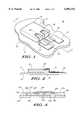
- FIG. 1is a perspective view of a circuit assembly in accordance with a preferred embodiment of the present invention.
- FIG. 2is a cross-section view along line 2--2 of FIG. 1.
- FIG. 3is a perspective view of a radio frequency identification tag in accordance with a preferred embodiment of the present invention.
- FIG. 4is a perspective view of a radio frequency identification tag in accordance with an alternative preferred embodiment of the present invention.
- FIG. 5is a cross-section view along line 5--5 of FIG. 4.
- FIG. 6is a perspective view of a circuit assembly in accordance with an alternate preferred embodiment of the present invention.
- FIG. 7is a perspective view of a circuit assembly in accordance with an alternate preferred embodiment of the present invention.
- FIG. 8is a cross-section view along line 8--8 of FIG. 7.
- FIG. 9is a perspective view of a radio frequency identification tag in accordance with an alternate preferred embodiment of the present invention.
- FIG. 10is a cross-section view along line 10--10 of FIG. 9.
- FIG. 11is a perspective view of a circuit assembly in accordance with an alternate preferred embodiment of the present invention.
- FIG. 12is a cross-section view along line 10--10 of FIG. 11.
- FIG. 13is a schematic illustration of an apparatus for printing interconnections in accordance with a preferred embodiment of the present invention.
- a circuit assemblyincludes a circuit chip secured to a substrate formed with a plurality of conductive traces.
- the circuit assemblymay also include additional circuit chips and components.
- the circuit chips and componentsare interconnected via the conductive traces and selective application of a printable conductive medium.
- a radio frequency identification tagincludes at least a radio frequency identification tag circuit chip and an antenna secured to a substrate formed with a number of conductive traces.
- the radio frequency identification tag circuit chip and the antennaare electrically coupled via the conductive traces and selective application of a printable conductive medium.
- a circuit assembly 10includes a circuit chip 12 secured to a substrate 14.
- substrate 14Preferred materials for substrate 14 include paper, synthetic paper, cardboard, plastic and the like.
- substrate 14is a high-temperature tolerant tape, such as Kapton tape, capable of withstanding elevated curing temperatures used during manufacture as well as operating temperatures of circuit assembly 10.
- Formed on a surface 16 of substrate 14are a plurality of conductive traces shown generally as a conductive trace 18 and a conductive trace 20.
- Conductive trace 18 and conductive trace 20are preferably formed by printing using a conductive medium such as conductive ink the desired pattern of traces on surface 16.
- Circuit chip 12is preferably bonded or otherwise secured to surface 16.
- Circuit chip 12may be of virtually any type of integrated circuit chip construction and further includes formed on, and possibly recessed into, an upper surface 22 a first conductive pad 26 and a second conductive pad 28. It will be appreciated that circuit chip 12 may be formed to include additional conductive pads, as the application requires and/or its physical size permits.
- Electrically coupling conductive pad 26 to conductive trace 18is a layer 30 of a conductive medium
- electrically coupling conductive pad 28 to conductive trace 20is a layer 32 of a conductive medium. As seen in FIG. 1 and FIG. 2, layer 32 is substantially uniform in thickness and extends continuously from conductive pad 28 along an edge 34 of circuit chip 12 to conductive trace 20.
- Layer 30similarly extends from conductive pad 26 to conductive trace 18.
- a suitable conductive medium for forming layer 30 and layer 32is conductive ink, such as a carbon/graphite bearing ink or a metal, either precious or non-precious, bearing ink.
- the conductive mediumis preferably applied using a printing technique, such as and without limitation, jet printing, screen printing, and pad transfer printing.
- Alternative conductive mediumsinclude conductive adhesive (isotropic or anisotropic), conductive polymers and the like.
- the thickness of circuit assembly 10is not substantially greater than the thickness of substrate 14 and the thickness of circuit chip 12.
- circuit assembly 10may be constructed to a thickness substantially less than that possible using either bumped pad circuit chips or wire bonding.
- circuit assembly 10is well adapted for, among other applications, constructing radio frequency identification tags.
- a radio frequency identification tag 100includes a radio frequency identification tag circuit chip ("circuit chip") 112 secured to substrate 114.
- Circuit chip 112includes a first conductive pad 126 and a second conductive pad 128 formed in an upper surface 127.
- Radio frequency identification tag 100is arranged as an inductive coupled device and thus includes a coil antenna 148 formed from insulated magnetic wire and including a first antenna lead 150 and a second antenna lead 154. Each of first antenna lead 150 and second antenna lead 154 is formed to include a stripped portion 152 and a second stripped portion 156, respectively. It will be appreciated that radio frequency identification tag 100 is shown and described in an exemplary embodiment of the present invention as an inductive coupling type radio frequency identification tag.
- Radio frequency identification tag 100also includes a circuit component 140, such as a resonating capacitor, including a first circuit component conductive pad 142 and a second circuit component conductive pad 144.
- circuit component 140such as a resonating capacitor
- Each of circuit chip 112, circuit component 140 and antenna 148are preferably bonded to a surface 1 16 of substrate 114.
- each of circuit chip 112, circuit component 140 and antenna 148are operatively, electrically coupled by a layer 130 and a layer 132 of conductive medium.
- a suitable conductive mediumis preferably a conductive ink, conductive polymer, conductive adhesive (isotropic or anisotropic) or the like printed onto surface 116.
- layer 130is formed to include a coupling portion 136.
- Layer 130electrically couples to conductive pad 126 and extends along surface 116 to coupling portion 136.
- Coupling portion 136is formed to electrically couple conductive pad 144 and stripped portion 156. In this manner, layer 130 interconnects each of conductive pad 126, conductive pad 144 and stripped portion 156.
- layer 132is formed to include a coupling portion 138, and is arranged to operatively, electrically couple conductive pad 128, conductive pad 142 and stripped portion 152.
- each of circuit chip 112, circuit component 140 and antenna 148are bonded or otherwise secured to surface 116.
- each of layer 130 and layer 132is applied, preferably using a printing technique, to electrically and operably couple the components.
- Layer 130 and layer 132do not add substantially to the thickness of radio frequency identification tag 100.
- a thickness of radio frequency identification tag 100is not substantially greater than a thickness of substrate 114 and the thickest of circuit chip 112, circuit component 140 and antenna 148.
- Radio frequency identification tag 200in accordance with an alternate preferred embodiment of the present invention is shown.
- Radio frequency identification tag 200includes a circuit chip 212 having a first conductive pad 226 and a second conductive pad 228 formed in an upper surface 227.
- Radio frequency identification tagalso includes an antenna (not shown) including a first lead 250 and a second lead 254 formed, respectively, to include a stripped portion 252 and a stripped portion 256.
- a circuit component 240 formed to include a first circuit component conductive pad 244 and a second circuit component conductive pad 246is also included.
- a template 258is also provided bonded to a surface 216 of substrate 214.
- Template 258is formed to include a circuit chip recess 260, a circuit component recess 262, a first antenna lead recess 264 and a second antenna lead recess 266. It will be appreciated that a separate template element need not be provided, and instead, substrate 214 may be formed with recessed regions corresponding respectively to each of the above-described recesses 260-266.
- circuit chip 212is disposed within circuit chip recess 260 and is bonded to surface 216.
- circuit component 240is disposed within circuit component recess 262, stripped portion 252 is disposed within recess 266 and stripped portion 256 is disposed within recess 264 with each of the respective elements being secured, preferably bonded, to surface 216.
- Each of recess 260, recess 262, recess 264 and recess 266are formed to allow the respective elements to be positioned below an upper surface 270 of template 258. In this manner the elements are protected from detachment during use of radio frequency identification tag 200.
- a first layer 236 and a second layer 238 of conductive mediumare provided to operatively, electrically couple circuit chip 212, circuit component 240, stripped portion 252 and stripped portion 256.
- a suitable conductive mediumis preferably a conductive ink, a conductive polymer or a conductive adhesive (isotropic or anisotropic).
- Layer 236 and layer 238is preferably printed using a suitable printing technique to surface 270. More particularly, layer 236 is arranged to couple conductive pad 226, conductive pad 244 and stripped portion 256. Similarly, layer 238 is arranged to couple conductive pad 228, conductive pad 246 and stripped portion 252.
- layer 236 and layer 238do not add substantially to the overall thickness radio frequency identification tag 200.
- the overall thickness of radio frequency identification tag 200is thus approximately the thickness of substrate 214 and template 258.
- circuit chip 212, circuit component 240, stripped portion 252 and stripped portion 256are protected in operation by template 258.
- a circuit assembly 300 in accordance with an alternate preferred embodiment of the present inventionincludes a first circuit chip 312 and a second circuit chip 340 secured to a surface 316 of a substrate 314.
- First circuit chip 312includes a first conductive pad 326 and a second conductive pad 328.
- Second circuit chip 340includes a first conductive pad 342 formed in an upper surface 345.
- Second circuit chip 340may include a second conductive pad 344 formed in upper surface 345 or a conductive pad (not shown) formed in a wall portion or on a bottom portion of second circuit chip 340.
- a first layer 330 and a second layer 332are provided to operatively, electrically couple first circuit chip 312 and second circuit chip 340.
- a suitable conductive mediumis a conductive ink, a conductive polymer, a conductive adhesive (isotropic or anisotropic), or the like, applied using a printing technique.
- Layer 330is applied to couple first conductive pad 326 to second circuit chip 340. More particularly, layer 330 includes a coupling region 350 disposed around and below second circuit chip 340 and electrically coupling to the second conductive pad.
- Layer 332is electrically coupled to second conductive pad 328 and extends longitudinally along surface 316.
- a coupling region 338is provided, consisting of a conductive medium also printed on surface 316, and couples layer 332 to first conductive pad 342.
- circuit assembly 300provides for a simplified manufacturing process.
- first circuit chip 312is secured to surface 316, preferably using pick-and-place automation.
- layer 330 and layer 332are printed onto surface 316.
- Second circuit chip 340is then secured to surface 316 also using pick-and-place automation.
- Second circuit chip 340is positioned into layer 330 forming coupling region 350 coupling to the second conductive pad.
- coupling region 338is formed, again by printing, coupling layer 330 to first conductive pad 342.
- a circuit chip assembly 400includes a circuit chip 412 secured to a surface 416 of a substrate 414.
- Substrate 414is also formed to include a plurality of conductive traces, generally indicated by conductive trace 418 and conductive trace 420. In certain applications it may be required to insulate an edge 434 of circuit chip 412. In such applications, following bonding of circuit chip 412 to surface 416 a layer of insulating material 464 is applied along edge 434.
- a first layer 430 and a second layer 432 of conductive mediumare provided for operatively, electrically coupling circuit chip 412 to conductive trace 418 and conductive trace 420.
- a suitable conductive mediumis a conductive ink, a conductive polymer, a conductive adhesive (isotropic or anisotropic) or the like applied using a printing technique.
- a radio frequency identification tag 500in accordance with a preferred embodiment of the present invention includes a radio frequency identification tag circuit chip ("circuit chip") 512 secured to a surface 516 of a substrate 514.
- Radio frequency identification tag 500is arranged to operate as a capacitive coupled device, and as such substrate 514 is formed to include a first antenna element 566 and a second antenna element 568.
- Each of first antenna element 566 and second antenna element 568is preferably formed by printing a conductive pattern on surface 516 using a conductive ink or other suitable conductive medium.
- First antenna element 566is coupled to a conductive trace 518 and second antenna element 568 is coupled to a conductive trace 520.
- Each of conductive trace 518 and conductive trace 520is also formed by printing, preferably at the same time as printing first antenna element 566 and second antenna element 568, using a conductive ink or other suitable conductive medium.
- Circuit chip 512includes a first conductive pad 526 and a second conductive pad 528, and circuit chip 512 is secured to surface 516.
- a first layer 530 and a second layer 532 of a conductive mediumare provided and operatively, electrically couple circuit chip 512 to conductive trace 518 and conductive trace 520.
- a suitable conductive mediumis a conductive ink, a conductive polymer, a conductive adhesive (isotropic or anisotropic) or the like preferably applied using a printing technique.
- Layer 530is applied to couple first conductive pad 526 to conductive trace 518, and layer 532 is applied to couple second conductive pad 528 to second conductive trace 520.
- layer 530 and layer 532do not add substantially to the thickness of radio frequency identification tag 500.
- a thickness of radio frequency identification tag 500is not substantially greater than a thickness of substrate 514 and the thickness of circuit chip 512.
- radio frequency identification tag 500is efficiently and cost effectively manufactured.
- a circuit assembly 600 in accordance with a preferred embodiment of the present inventionincludes a circuit chip 612 disposed within a recess 670 formed in a surface 616 of substrate 614.
- Substrate 614is further formed to include a plurality of conductive traces generally indicated as conductive trace 618 and conductive trace 620. Conductive trace 618 and conductive trace 620 are arranged to interconnect with virtually any number of additional circuit elements (not shown) associated with circuit assembly 600.
- Circuit chip 612includes a first conductive pad 626 and a second conductive pad 628 formed in an upper surface 627. Circuit chip 612 is operatively, electrically coupled to conductive trace 618 and conductive trace 620 by a layer 630 and a layer 632, respectively, of a conductive medium.
- a suitable conductive mediumis a conductive ink, a conductive polymer, a conductive adhesive (isotropic or anisotropic) or the like. More particularly, layer 630 couples conductive pad 626 to conductive trace 618, and layer 632 couples conductive pad 628 to conductive trace 620.
- circuit chip 612is disposed within recess 670 such that upper surface 627 is at or below surface 616.
- Layer 630 and layer 632do not add substantially to the thickness of circuit assembly 600.
- the overall thickness of circuit assembly 600is not substantially greater than the thickness of substrate 614, which is not substantially greater than the thickness of circuit chip 612.
- An insulating material 672may be disposed within recess 670 and around circuit chip 612. Therefore, circuit assembly 600 is well adapted for, among other applications, constructing radio frequency identification tags.
- Apparatus 700includes a resilient printing pad 702 secured to an articulating apparatus (not shown) as is well known in the art. The action of the articulating apparatus is illustrated in phantom.
- An inking plate 704is etched with a pattern 706 corresponding to the configuration of the layers to be printed.
- Conductive mediumsuch as conductive ink, is applied to pattern 706.
- Resilient pad 702is brought into contact with plate 704 and the conductive medium is transferred from pattern 706 to pad 702.
- Pad 702is then aligned to and brought into contact with a substrate 708. The conductive medium is transferred from pad 702 to substrate 708, and pad 702 is lifted away from substrate 708.
- substrate 708is a continuous sheet of material, such as Kapton tape, which is later separated into individual circuit assemblies. After the conductive medium is transferred substrate 708, substrate may be passed through a curing oven 701, if necessary, to fast dry the conductive medium. It is expected that apparatus 700 will form a portion of a comprehensive manufacturing process including circuit chip placement automation and other related processing to produce completed radio frequency identification tags in accordance with the present invention.
- a circuit assemblyincludes a substrate formed to include a conductive trace and a circuit chip secured to the substrate.
- the circuit chipincludes a conductive pad, and a layer of conductive medium is printed on the substrate and coupling the conductive pad to the conductive trace.
- the substratemay also include a circuit chip recess with the circuit chip being secured to the substrate within the recess.
- a radio frequency identification tagincludes a substrate formed to include a conductive trace.
- a radio frequency identification tag circuit chipis secured to the substrate, and the radio frequency identification tag circuit chip includes a conductive pad.
- a layer of conductive mediumis printed on the substrate and couples the conductive pad to the conductive trace.
- a radio frequency identification tagincludes a substrate, a radio frequency identification tag circuit chip secured to the substrate and an antenna secured to the substrate.
- the radio frequency identification tag circuit chiphas a first conductive pad and a second conductive pad, and the antenna has a first antenna lead and a second antenna lead.
- a first layer of conductive mediumis printed on the substrate coupling the first conductive pad to the first antenna lead and a second layer of conductive medium is printed on the substrate coupling the second conductive pad to the second antenna lead.
- a radio frequency identification tagin another alternative embodiment, and with reference to FIG. 4, includes a substrate having plurality of conductive traces formed on a surface and a template secured to the surface.
- the templateincludes a circuit chip recess, and a radio frequency identification tag circuit chip is disposed within the recess and secured to the surface.
- the radio frequency identification tag circuit chipincludes a conductive pad, and a layer of conductive medium is printed on the template coupling the conductive pad to at least one of the plurality of conductive traces.
- the present inventionovercomes the thickness limitations posed by either of flip chip technology or wire loop bonding technology.
- the present inventionpermits, and at substantially reduced cost, coupling of radio frequency identification tag circuit chips to thin substrates formed to include printed conductive traces.
- the present inventionadvantageously avoids costly flip chip technology and the associated process handling difficulties in permitting circuit chips to be secured to the substrates conductive pads up.
- the present inventionfurther provides a cost effective, processing efficient alternative to wire loop bonding technology and its associated wire loop bond height and rigid substrate material limitations.
Landscapes
- Engineering & Computer Science (AREA)
- Microelectronics & Electronic Packaging (AREA)
- Computer Hardware Design (AREA)
- Physics & Mathematics (AREA)
- General Physics & Mathematics (AREA)
- Theoretical Computer Science (AREA)
- Power Engineering (AREA)
- Mechanical Engineering (AREA)
- Condensed Matter Physics & Semiconductors (AREA)
- Computer Networks & Wireless Communication (AREA)
- Credit Cards Or The Like (AREA)
Abstract
Description
Claims (34)
Priority Applications (2)
| Application Number | Priority Date | Filing Date | Title |
|---|---|---|---|
| US09/115,279US6091332A (en) | 1998-06-09 | 1998-07-14 | Radio frequency identification tag having printed circuit interconnections |
| US09/393,097US6246327B1 (en) | 1998-06-09 | 1999-09-09 | Radio frequency identification tag circuit chip having printed interconnection pads |
Applications Claiming Priority (3)
| Application Number | Priority Date | Filing Date | Title |
|---|---|---|---|
| US09/094,261US6107920A (en) | 1998-06-09 | 1998-06-09 | Radio frequency identification tag having an article integrated antenna |
| US09/103,226US6018299A (en) | 1998-06-09 | 1998-06-23 | Radio frequency identification tag having a printed antenna and method |
| US09/115,279US6091332A (en) | 1998-06-09 | 1998-07-14 | Radio frequency identification tag having printed circuit interconnections |
Related Parent Applications (2)
| Application Number | Title | Priority Date | Filing Date |
|---|---|---|---|
| US09/094,261Continuation-In-PartUS6107920A (en) | 1998-06-09 | 1998-06-09 | Radio frequency identification tag having an article integrated antenna |
| US09/103,226Continuation-In-PartUS6018299A (en) | 1998-06-09 | 1998-06-23 | Radio frequency identification tag having a printed antenna and method |
Related Child Applications (1)
| Application Number | Title | Priority Date | Filing Date |
|---|---|---|---|
| US09/393,097Continuation-In-PartUS6246327B1 (en) | 1998-06-09 | 1999-09-09 | Radio frequency identification tag circuit chip having printed interconnection pads |
Publications (1)
| Publication Number | Publication Date |
|---|---|
| US6091332Atrue US6091332A (en) | 2000-07-18 |
Family
ID=46203399
Family Applications (1)
| Application Number | Title | Priority Date | Filing Date |
|---|---|---|---|
| US09/115,279Expired - LifetimeUS6091332A (en) | 1998-06-09 | 1998-07-14 | Radio frequency identification tag having printed circuit interconnections |
Country Status (1)
| Country | Link |
|---|---|
| US (1) | US6091332A (en) |
Cited By (114)
| Publication number | Priority date | Publication date | Assignee | Title |
|---|---|---|---|---|
| US6229100B1 (en)* | 1996-11-27 | 2001-05-08 | Tessera, Inc. | Low profile socket for microelectronic components and method for making the same |
| US6246327B1 (en)* | 1998-06-09 | 2001-06-12 | Motorola, Inc. | Radio frequency identification tag circuit chip having printed interconnection pads |
| US6259369B1 (en)* | 1999-09-30 | 2001-07-10 | Moore North America, Inc. | Low cost long distance RFID reading |
| US6304185B1 (en) | 1999-08-12 | 2001-10-16 | Micron Technology, Inc. | Devices for sensing living organisms, devices for sensing termites, methods of forming devices for sensing termites, and methods for sensing termites |
| US6313748B1 (en) | 1999-08-27 | 2001-11-06 | Micron Technology, Inc. | Electrical apparatuses, termite sensing apparatuses, methods of forming electrical apparatuses, and methods of sensing termites |
| US6323772B1 (en) | 1999-08-12 | 2001-11-27 | Micron Technology, Inc. | Devices for sensing termites and other living organisms, and methods of forming devices for sensing termites |
| WO2002011095A1 (en)* | 2000-08-02 | 2002-02-07 | Motorola, Inc. | Capacitively powered radio frequency identification device |
| US6373391B1 (en) | 1999-08-12 | 2002-04-16 | Micron Technology, Inc. | Devices for sensing changes in environments proximate the devices, devices for sensing termites, and methods for sensing termites |
| US6392545B2 (en)* | 1999-08-27 | 2002-05-21 | Micron Technology, Inc. | Electrical apparatuses, and methods of forming electrical apparatuses |
| WO2002050904A1 (en)* | 2000-12-21 | 2002-06-27 | Gemplus | Connection by printed-weld deformable member |
| WO2002050903A1 (en)* | 2000-12-21 | 2002-06-27 | Gemplus | Cut-out insulating member and contact-weld connection |
| US6424263B1 (en)* | 2000-12-01 | 2002-07-23 | Microchip Technology Incorporated | Radio frequency identification tag on a single layer substrate |
| US6451154B1 (en) | 2000-02-18 | 2002-09-17 | Moore North America, Inc. | RFID manufacturing concepts |
| FR2823011A1 (en)* | 2001-03-30 | 2002-10-04 | Gemplus Card Int | Electrical connection of integrated circuit output contact to communication interface contact, for chip card, involves deposition of conductive lead on connection region delimited by insulating mask |
| US20020145036A1 (en)* | 2001-04-04 | 2002-10-10 | Otto Jerome A. | Radio frequency identification system and method |
| US20020152604A1 (en)* | 2001-04-23 | 2002-10-24 | Debraal John Charles | Method and system for forming electrically conductive pathways |
| US6480110B2 (en) | 2000-12-01 | 2002-11-12 | Microchip Technology Incorporated | Inductively tunable antenna for a radio frequency identification tag |
| US20020183979A1 (en)* | 2001-05-08 | 2002-12-05 | Wildman Timothy D. | Article locating and tracking system |
| US20030047350A1 (en)* | 2001-09-11 | 2003-03-13 | Forbes Brian S. | Embedded PCB identification |
| US20030063002A1 (en)* | 2001-09-28 | 2003-04-03 | Hitachi, Ltd. | Method of manufacturing electronic tag |
| US20030136503A1 (en)* | 2002-01-18 | 2003-07-24 | Avery Dennison Corporation | RFID label technique |
| US20030156501A1 (en)* | 2002-01-14 | 2003-08-21 | Martin Spindel | Trackable storage unit system and method |
| US20030170010A1 (en)* | 2002-03-08 | 2003-09-11 | Shining Technology, Inc. A California Corporation | System and method for direct recording of audio, video and/or images for easy access and editing |
| US6665044B1 (en) | 1999-02-05 | 2003-12-16 | Alien Technology Corporation | Apparatuses and methods for forming electronic assemblies |
| US6665193B1 (en)* | 2002-07-09 | 2003-12-16 | Amerasia International Technology, Inc. | Electronic circuit construction, as for a wireless RF tag |
| US6667092B1 (en) | 2002-09-26 | 2003-12-23 | International Paper Company | RFID enabled corrugated structures |
| US20040020040A1 (en)* | 2002-08-02 | 2004-02-05 | Matrics, Inc. | Method and system for forming a die frame for transferring dies therewith |
| US20040020036A1 (en)* | 2002-08-02 | 2004-02-05 | Matrics, Inc. | Method and apparatus for high volume assembly of radio frequency identification tags |
| US6693541B2 (en) | 2001-07-19 | 2004-02-17 | 3M Innovative Properties Co | RFID tag with bridge circuit assembly and methods of use |
| US6696952B2 (en)* | 2000-08-04 | 2004-02-24 | Hei, Inc. | Structures and assembly methods for radio-frequency-identification modules |
| US20040049428A1 (en)* | 2002-09-05 | 2004-03-11 | Soehnlen John Pius | Wireless environmental sensing in packaging applications |
| US20040070504A1 (en)* | 2002-10-14 | 2004-04-15 | Brollier Brian W. | Semi-covert RFID enabled containers |
| US20040068864A1 (en)* | 1999-02-05 | 2004-04-15 | Hadley Mark A. | Web fabrication of devices |
| US6731353B1 (en) | 2001-08-17 | 2004-05-04 | Alien Technology Corporation | Method and apparatus for transferring blocks |
| US20040102870A1 (en)* | 2002-11-26 | 2004-05-27 | Andersen Scott Paul | RFID enabled paper rolls and system and method for tracking inventory |
| US20040154161A1 (en)* | 2003-02-07 | 2004-08-12 | Hallys Corporation | Random-period chip transfer apparatus |
| US6779246B2 (en) | 2001-04-23 | 2004-08-24 | Appleton Papers Inc. | Method and system for forming RF reflective pathways |
| US20040183182A1 (en)* | 2002-01-23 | 2004-09-23 | Susan Swindlehurst | Apparatus incorporating small-feature-size and large-feature-size components and method for making same |
| US20040193449A1 (en)* | 2002-09-27 | 2004-09-30 | Wildman Timothy D. | Universal communications, monitoring, tracking, and control system for a healthcare facility |
| US6816380B2 (en) | 2001-05-31 | 2004-11-09 | Alien Technology Corporation | Electronic devices with small functional elements supported on a carrier |
| US20040250417A1 (en)* | 2003-06-12 | 2004-12-16 | Arneson Michael R. | Method, system, and apparatus for transfer of dies using a die plate |
| US20050001785A1 (en)* | 2002-12-31 | 2005-01-06 | Ferguson Scott Wayne | RFID device and method of forming |
| US20050000634A1 (en)* | 2003-05-16 | 2005-01-06 | Craig Gordon S.W. | Transfer assembly for manufacturing electronic devices |
| US20050026414A1 (en)* | 2000-02-24 | 2005-02-03 | Williams Vernon M. | Methods for consolidating previously unconsolidated conductive material to form conductive structures or contact pads or secure conductive structures to contact pads |
| US20050035924A1 (en)* | 2002-12-31 | 2005-02-17 | Peikang Liu | RFID device and method of forming |
| US20050035862A1 (en)* | 2001-05-08 | 2005-02-17 | Wildman Timothy D. | Article locating and tracking apparatus and method |
| US20050046018A1 (en)* | 1999-03-16 | 2005-03-03 | Jacobsen Jeffrey Jay | Electronic devices with small functional elements supported on a carrier |
| US20050052283A1 (en)* | 2003-09-09 | 2005-03-10 | Collins Timothy J. | Method and apparatus for multiple frequency RFID tag architecture |
| US6866752B2 (en) | 2001-08-23 | 2005-03-15 | The United States Of America As Represented By The Administrator Of The National Aeronautics And Space Administration | Method of forming ultra thin film devices by vacuum arc vapor deposition |
| US20050151699A1 (en)* | 2004-01-12 | 2005-07-14 | Symbol Technologies, Inc. | Method and system for manufacturing radio frequency identification tag antennas |
| US20050155213A1 (en)* | 2004-01-12 | 2005-07-21 | Symbol Technologies, Inc. | Radio frequency identification tag inlay sortation and assembly |
| US20050196524A1 (en)* | 1999-03-16 | 2005-09-08 | Jacobsen Jeffrey J. | Apparatuses and methods for forming assemblies |
| US20050224590A1 (en)* | 2004-04-13 | 2005-10-13 | John Melngailis | Method and system for fabricating integrated circuit chips with unique identification numbers |
| US20060012387A1 (en)* | 2004-06-29 | 2006-01-19 | Symbol Technologies, Inc. | Systems and methods for testing radio frequency identification tags |
| US20060036346A1 (en)* | 2002-11-26 | 2006-02-16 | Andersen Scott P | System and method for tracking inventory |
| US20060038687A1 (en)* | 2004-08-17 | 2006-02-23 | Symbol Technologies, Inc. | Singulation of radio frequency identification (RFID) tags for testing and/or programming |
| US20060055014A1 (en)* | 2004-09-14 | 2006-03-16 | Semiconductor Energy Laboratory Co., Ltd. | Wireless chip and manufacturing method of the same |
| US20060063323A1 (en)* | 2004-09-22 | 2006-03-23 | Jason Munn | High-speed RFID circuit placement method and device |
| US7042337B2 (en) | 1997-11-07 | 2006-05-09 | Hill-Rom Services, Inc. | Communication and data entry device |
| US20060109123A1 (en)* | 2004-11-22 | 2006-05-25 | Curt Carrender | Radio frequency identification (RFID) tag for an item having a conductive layer included or attached |
| US20060185790A1 (en)* | 2004-02-23 | 2006-08-24 | Eric Eckstein | Security tag & method using a flowable material |
| US20060202269A1 (en)* | 2005-03-08 | 2006-09-14 | Semiconductor Energy Laboratory Co., Ltd. | Wireless chip and electronic appliance having the same |
| US20060202841A1 (en)* | 2001-11-08 | 2006-09-14 | Sleep Diagnostics, Pty., Ltd. | Alertness monitor |
| US20060223225A1 (en)* | 2005-03-29 | 2006-10-05 | Symbol Technologies, Inc. | Method, system, and apparatus for transfer of integrated circuit dies using an attractive force |
| US20060225273A1 (en)* | 2005-03-29 | 2006-10-12 | Symbol Technologies, Inc. | Transferring die(s) from an intermediate surface to a substrate |
| US20060238345A1 (en)* | 2005-04-25 | 2006-10-26 | Ferguson Scott W | High-speed RFID circuit placement method and device |
| US20060261950A1 (en)* | 2005-03-29 | 2006-11-23 | Symbol Technologies, Inc. | Smart radio frequency identification (RFID) items |
| US20060267778A1 (en)* | 2003-03-24 | 2006-11-30 | Gengel Gleen W | RFID tags and processes for producing RFID tags |
| US20060267200A1 (en)* | 2005-05-13 | 2006-11-30 | University Of Pittsburgh - Of The Commonwealth System Of Higher Education | Method of making an electronic device using an electrically conductive polymer, and associated products |
| US20070007661A1 (en)* | 2005-06-09 | 2007-01-11 | Burgess Lester E | Hybrid conductive coating method for electrical bridging connection of RFID die chip to composite antenna |
| US20070012773A1 (en)* | 2005-06-07 | 2007-01-18 | University Of Pittsburgh - Of The Commonwealth System Of Higher Education | Method of making an electronic device using an electrically conductive polymer, and associated products |
| US20070031992A1 (en)* | 2005-08-05 | 2007-02-08 | Schatz Kenneth D | Apparatuses and methods facilitating functional block deposition |
| US20070080801A1 (en)* | 2003-10-16 | 2007-04-12 | Weismiller Matthew W | Universal communications, monitoring, tracking, and control system for a healthcare facility |
| US20070107186A1 (en)* | 2005-11-04 | 2007-05-17 | Symbol Technologies, Inc. | Method and system for high volume transfer of dies to substrates |
| US20070115131A1 (en)* | 2003-11-25 | 2007-05-24 | Ntn Corporation | Bearing with ic tag and seal for the same |
| US20070115645A1 (en)* | 2001-08-17 | 2007-05-24 | Jacobsen Jeffrey J | Apparatuses and methods for forming wireless RF labels |
| WO2007060631A1 (en) | 2005-11-28 | 2007-05-31 | Nxp B.V. | A method of producing a transponder and a transponder |
| WO2007060630A1 (en) | 2005-11-28 | 2007-05-31 | Nxp B.V. | Device comprising a substrate including an electric contact, and transponder |
| US20070131016A1 (en)* | 2005-12-13 | 2007-06-14 | Symbol Technologies, Inc. | Transferring die(s) from an intermediate surface to a substrate |
| US20070141760A1 (en)* | 2005-12-21 | 2007-06-21 | Ferguson Scott W | Electrical device and method of manufacturing electrical devices using film embossing techniques to embed integrated circuits into film |
| US20070139057A1 (en)* | 2005-12-15 | 2007-06-21 | Symbol Technologies, Inc. | System and method for radio frequency identification tag direct connection test |
| US20070144662A1 (en)* | 2005-12-22 | 2007-06-28 | Armijo Edward A | Method of manufacturing RFID devices |
| US20070158024A1 (en)* | 2006-01-11 | 2007-07-12 | Symbol Technologies, Inc. | Methods and systems for removing multiple die(s) from a surface |
| US20070187496A1 (en)* | 2006-02-10 | 2007-08-16 | Andersen Scott P | Inventory tracking system and method |
| DE102006008948B3 (en)* | 2006-02-23 | 2007-10-04 | Mühlbauer Ag | Method for applying and electrically contacting electronic components to a substrate web |
| US20070244657A1 (en)* | 2006-04-11 | 2007-10-18 | Drago Randall A | Methods and systems for testing radio frequency identification (RFID) tags having multiple antennas |
| US20070273515A1 (en)* | 2004-10-08 | 2007-11-29 | Mackenzie J D | RF and/or RF identification tag/device having an integrated interposer, and methods for making and using the same |
| US7353598B2 (en) | 2004-11-08 | 2008-04-08 | Alien Technology Corporation | Assembly comprising functional devices and method of making same |
| US7385284B2 (en)* | 2004-11-22 | 2008-06-10 | Alien Technology Corporation | Transponder incorporated into an electronic device |
| US20080150725A1 (en)* | 2006-09-29 | 2008-06-26 | Nobuaki Takahashi | Rfid label tag and method of manufacturing the same |
| US7417306B1 (en) | 2001-08-17 | 2008-08-26 | Alien Technology Corporation | Apparatuses and methods for forming electronic assemblies |
| US20080272885A1 (en)* | 2004-01-22 | 2008-11-06 | Mikoh Corporation | Modular Radio Frequency Identification Tagging Method |
| US7452748B1 (en) | 2004-11-08 | 2008-11-18 | Alien Technology Corporation | Strap assembly comprising functional block deposited therein and method of making same |
| DE112006002993T5 (en) | 2005-11-09 | 2008-11-20 | Motorola, Inc., Schaumburg | Short-range detection system for providing wireless authentication |
| US20080315311A1 (en)* | 2007-06-22 | 2008-12-25 | Semiconductor Energy Laboratory Co., Ltd. | Semiconductor device |
| US7534045B2 (en) | 2003-11-25 | 2009-05-19 | Ntn Corporation | Bearing with IC tag and seal for the same |
| US7542301B1 (en) | 2005-06-22 | 2009-06-02 | Alien Technology Corporation | Creating recessed regions in a substrate and assemblies having such recessed regions |
| US7551141B1 (en) | 2004-11-08 | 2009-06-23 | Alien Technology Corporation | RFID strap capacitively coupled and method of making same |
| US20100127084A1 (en)* | 2008-11-25 | 2010-05-27 | Vikram Pavate | Printed Antennas, Methods of Printing an Antenna, and Devices Including the Printed Antenna |
| US7838892B2 (en) | 2004-04-29 | 2010-11-23 | Osram Opto Semiconductors Gmbh | Optoelectronic semiconductor chip and method for forming a contact structure for making electrical contact with an optoelectronic semiconductor chip |
| US7855648B2 (en) | 2007-08-14 | 2010-12-21 | Avery Dennison Corporation | RFID tag |
| WO2011103508A1 (en)* | 2010-02-19 | 2011-08-25 | Cubic Corporation | Smartcard interconnect |
| US20150223323A1 (en)* | 2014-02-05 | 2015-08-06 | Colin Patrick O'Flynn | Footprint for Prototyping High Frequency Printed Circuit Boards |
| US20170194171A1 (en)* | 2014-06-06 | 2017-07-06 | Rohinni, LLC | Manufacture of Circuit Assembly with Unpackaged Semiconductor Devices |
| US9830424B2 (en) | 2013-09-18 | 2017-11-28 | Hill-Rom Services, Inc. | Bed/room/patient association systems and methods |
| US20180121976A1 (en)* | 2002-06-17 | 2018-05-03 | Philip Morris Usa Inc. | System for coupling package displays to remote power source |
| US10242971B2 (en) | 2015-03-20 | 2019-03-26 | Rohinni, LLC | Apparatus for direct transfer of semiconductor devices with needle retraction support |
| US10354895B2 (en) | 2017-01-18 | 2019-07-16 | Rohinni, LLC | Support substrate for transfer of semiconductor devices |
| US10700052B2 (en) | 2015-01-12 | 2020-06-30 | Dolby Laboratories Licensing Corporation | Pixel tile structures and layouts |
| US11094571B2 (en) | 2018-09-28 | 2021-08-17 | Rohinni, LLC | Apparatus to increase transferspeed of semiconductor devices with micro-adjustment |
| US20210297057A1 (en)* | 2018-12-21 | 2021-09-23 | Murata Manufacturing Co., Ltd. | Method for manufacturing electronic component module and electronic component module |
| US11189592B2 (en)* | 2018-10-02 | 2021-11-30 | Infineon Technologies Austria Ag | Multi-clip structure for die bonding |
| US11462433B2 (en) | 2016-11-23 | 2022-10-04 | Rohinni, LLC | Direct transfer apparatus for a pattern array of semiconductor device die |
| US11911325B2 (en) | 2019-02-26 | 2024-02-27 | Hill-Rom Services, Inc. | Bed interface for manual location |
Citations (5)
| Publication number | Priority date | Publication date | Assignee | Title |
|---|---|---|---|---|
| US3934336A (en)* | 1975-01-13 | 1976-01-27 | Burroughs Corporation | Electronic package assembly with capillary bridging connection |
| US4759970A (en)* | 1984-10-25 | 1988-07-26 | Amoco Corporation | Electronic carrier devices and methods of manufacture |
| US5528222A (en)* | 1994-09-09 | 1996-06-18 | International Business Machines Corporation | Radio frequency circuit and memory in thin flexible package |
| US5566441A (en)* | 1993-03-11 | 1996-10-22 | British Technology Group Limited | Attaching an electronic circuit to a substrate |
| US5768109A (en)* | 1991-06-26 | 1998-06-16 | Hughes Electronics | Multi-layer circuit board and semiconductor flip chip connection |
- 1998
- 1998-07-14USUS09/115,279patent/US6091332A/ennot_activeExpired - Lifetime
Patent Citations (5)
| Publication number | Priority date | Publication date | Assignee | Title |
|---|---|---|---|---|
| US3934336A (en)* | 1975-01-13 | 1976-01-27 | Burroughs Corporation | Electronic package assembly with capillary bridging connection |
| US4759970A (en)* | 1984-10-25 | 1988-07-26 | Amoco Corporation | Electronic carrier devices and methods of manufacture |
| US5768109A (en)* | 1991-06-26 | 1998-06-16 | Hughes Electronics | Multi-layer circuit board and semiconductor flip chip connection |
| US5566441A (en)* | 1993-03-11 | 1996-10-22 | British Technology Group Limited | Attaching an electronic circuit to a substrate |
| US5528222A (en)* | 1994-09-09 | 1996-06-18 | International Business Machines Corporation | Radio frequency circuit and memory in thin flexible package |
Cited By (255)
| Publication number | Priority date | Publication date | Assignee | Title |
|---|---|---|---|---|
| US6229100B1 (en)* | 1996-11-27 | 2001-05-08 | Tessera, Inc. | Low profile socket for microelectronic components and method for making the same |
| US7042337B2 (en) | 1997-11-07 | 2006-05-09 | Hill-Rom Services, Inc. | Communication and data entry device |
| US6246327B1 (en)* | 1998-06-09 | 2001-06-12 | Motorola, Inc. | Radio frequency identification tag circuit chip having printed interconnection pads |
| US20070002203A1 (en)* | 1999-02-05 | 2007-01-04 | Jacobsen Jeffrey J | Apparatuses and methods for forming assemblies |
| US6665044B1 (en) | 1999-02-05 | 2003-12-16 | Alien Technology Corporation | Apparatuses and methods for forming electronic assemblies |
| US20040068864A1 (en)* | 1999-02-05 | 2004-04-15 | Hadley Mark A. | Web fabrication of devices |
| US7561221B2 (en) | 1999-02-05 | 2009-07-14 | Alien Technology Corporation | Apparatuses and methods for forming assemblies |
| US6927085B2 (en) | 1999-02-05 | 2005-08-09 | Alien Technology Corporation | Web fabrication of devices |
| US7288432B2 (en) | 1999-03-16 | 2007-10-30 | Alien Technology Corporation | Electronic devices with small functional elements supported on a carrier |
| US20050046018A1 (en)* | 1999-03-16 | 2005-03-03 | Jacobsen Jeffrey Jay | Electronic devices with small functional elements supported on a carrier |
| US7070851B2 (en) | 1999-03-16 | 2006-07-04 | Alien Technology Corporation | Web process interconnect in electronic assemblies |
| US7425467B2 (en) | 1999-03-16 | 2008-09-16 | Alien Technology Corporation | Web process interconnect in electronic assemblies |
| US7172910B2 (en) | 1999-03-16 | 2007-02-06 | Alien Technology Corporation | Web fabrication of devices |
| US20080036087A1 (en)* | 1999-03-16 | 2008-02-14 | Jacobsen Jeffrey J | Web process interconnect in electronic assemblies |
| US20050196524A1 (en)* | 1999-03-16 | 2005-09-08 | Jacobsen Jeffrey J. | Apparatuses and methods for forming assemblies |
| US7113250B2 (en) | 1999-03-16 | 2006-09-26 | Alien Technology Corporation | Apparatuses and methods for forming assemblies |
| US6304185B1 (en) | 1999-08-12 | 2001-10-16 | Micron Technology, Inc. | Devices for sensing living organisms, devices for sensing termites, methods of forming devices for sensing termites, and methods for sensing termites |
| US6373391B1 (en) | 1999-08-12 | 2002-04-16 | Micron Technology, Inc. | Devices for sensing changes in environments proximate the devices, devices for sensing termites, and methods for sensing termites |
| US6323772B1 (en) | 1999-08-12 | 2001-11-27 | Micron Technology, Inc. | Devices for sensing termites and other living organisms, and methods of forming devices for sensing termites |
| US6630887B2 (en) | 1999-08-27 | 2003-10-07 | Micron Technology, Inc. | Electrical apparatuses, and methods of forming electrical apparatuses |
| US6313748B1 (en) | 1999-08-27 | 2001-11-06 | Micron Technology, Inc. | Electrical apparatuses, termite sensing apparatuses, methods of forming electrical apparatuses, and methods of sensing termites |
| US6392545B2 (en)* | 1999-08-27 | 2002-05-21 | Micron Technology, Inc. | Electrical apparatuses, and methods of forming electrical apparatuses |
| US6259369B1 (en)* | 1999-09-30 | 2001-07-10 | Moore North America, Inc. | Low cost long distance RFID reading |
| US6451154B1 (en) | 2000-02-18 | 2002-09-17 | Moore North America, Inc. | RFID manufacturing concepts |
| US20020195195A1 (en)* | 2000-02-18 | 2002-12-26 | Moore North America, Inc.. | RFID manufacturing concepts |
| US20020195194A1 (en)* | 2000-02-18 | 2002-12-26 | Moore North America, Inc.. | RFID manufacturing concepts |
| US7014729B2 (en) | 2000-02-18 | 2006-03-21 | Moore Wallace North America, Inc. | RFID manufacturing concepts |
| US7045186B2 (en) | 2000-02-18 | 2006-05-16 | Moore North America, Inc. | RFID manufacturing concepts |
| US20050221531A1 (en)* | 2000-02-24 | 2005-10-06 | Williams Vernon M | Carrier substrates and conductive elements thereof |
| US20070062033A1 (en)* | 2000-02-24 | 2007-03-22 | Williams Vernon M | Selective consolidation methods for fabricating semiconductor device components and conductive features thereof |
| US20050026414A1 (en)* | 2000-02-24 | 2005-02-03 | Williams Vernon M. | Methods for consolidating previously unconsolidated conductive material to form conductive structures or contact pads or secure conductive structures to contact pads |
| US20050230806A1 (en)* | 2000-02-24 | 2005-10-20 | Williams Vernon M | Conductive elements with adjacent, mutually adhered regions and semiconductor device assemblies including such conductive elements |
| US20050230843A1 (en)* | 2000-02-24 | 2005-10-20 | Williams Vernon M | Flip-chip type semiconductor devices and conductive elements thereof |
| WO2002011095A1 (en)* | 2000-08-02 | 2002-02-07 | Motorola, Inc. | Capacitively powered radio frequency identification device |
| US6384727B1 (en) | 2000-08-02 | 2002-05-07 | Motorola, Inc. | Capacitively powered radio frequency identification device |
| US6696952B2 (en)* | 2000-08-04 | 2004-02-24 | Hei, Inc. | Structures and assembly methods for radio-frequency-identification modules |
| US6424263B1 (en)* | 2000-12-01 | 2002-07-23 | Microchip Technology Incorporated | Radio frequency identification tag on a single layer substrate |
| US6480110B2 (en) | 2000-12-01 | 2002-11-12 | Microchip Technology Incorporated | Inductively tunable antenna for a radio frequency identification tag |
| US6496113B2 (en) | 2000-12-01 | 2002-12-17 | Microchip Technology Incorporated | Radio frequency identification tag on a single layer substrate |
| WO2002050904A1 (en)* | 2000-12-21 | 2002-06-27 | Gemplus | Connection by printed-weld deformable member |
| FR2818801A1 (en)* | 2000-12-21 | 2002-06-28 | Gemplus Card Int | INTERCONNECTION BY CUT-OUT INSULATION DEVICE AND CONDUCTION CORD |
| FR2818800A1 (en)* | 2000-12-21 | 2002-06-28 | Gemplus Card Int | INTERCONNECTION BY DEFORMABLE MEMBER FOR ELECTRONIC DEVICE |
| WO2002050903A1 (en)* | 2000-12-21 | 2002-06-27 | Gemplus | Cut-out insulating member and contact-weld connection |
| US9495632B2 (en) | 2001-02-02 | 2016-11-15 | Avery Dennison Corporation | RFID label technique |
| WO2002084586A1 (en)* | 2001-03-30 | 2002-10-24 | Gemplus | Connection by deposition of a conductive material bead on a connecting zone delimited by an insulating mask |
| FR2823011A1 (en)* | 2001-03-30 | 2002-10-04 | Gemplus Card Int | Electrical connection of integrated circuit output contact to communication interface contact, for chip card, involves deposition of conductive lead on connection region delimited by insulating mask |
| US6732923B2 (en) | 2001-04-04 | 2004-05-11 | Ncr Corporation | Radio frequency identification system and method |
| US20020145036A1 (en)* | 2001-04-04 | 2002-10-10 | Otto Jerome A. | Radio frequency identification system and method |
| US20020152604A1 (en)* | 2001-04-23 | 2002-10-24 | Debraal John Charles | Method and system for forming electrically conductive pathways |
| US6779246B2 (en) | 2001-04-23 | 2004-08-24 | Appleton Papers Inc. | Method and system for forming RF reflective pathways |
| US20050005856A1 (en)* | 2001-04-23 | 2005-01-13 | Appleton Papers Inc. | Method and system for forming RF reflective pathways |
| US6892441B2 (en) | 2001-04-23 | 2005-05-17 | Appleton Papers Inc. | Method for forming electrically conductive pathways |
| US7242306B2 (en) | 2001-05-08 | 2007-07-10 | Hill-Rom Services, Inc. | Article locating and tracking apparatus and method |
| US7248933B2 (en) | 2001-05-08 | 2007-07-24 | Hill-Rom Services, Inc. | Article locating and tracking system |
| US20020183979A1 (en)* | 2001-05-08 | 2002-12-05 | Wildman Timothy D. | Article locating and tracking system |
| US7450024B2 (en) | 2001-05-08 | 2008-11-11 | Hill-Rom Services, Inc. | Article locating and tracking apparatus and method |
| US20050035862A1 (en)* | 2001-05-08 | 2005-02-17 | Wildman Timothy D. | Article locating and tracking apparatus and method |
| US20050270752A1 (en)* | 2001-05-31 | 2005-12-08 | Credelle Thomas L | Electronic devices with small functional elements supported on a carrier |
| US6985361B2 (en) | 2001-05-31 | 2006-01-10 | Alien Technology Corporation | Electronic devices with small functional elements supported on a carrier |
| US6816380B2 (en) | 2001-05-31 | 2004-11-09 | Alien Technology Corporation | Electronic devices with small functional elements supported on a carrier |
| US7559131B2 (en) | 2001-05-31 | 2009-07-14 | Alien Technology Corporation | Method of making a radio frequency identification (RFID) tag |
| US8516683B2 (en) | 2001-05-31 | 2013-08-27 | Alien Technology Corporation | Methods of making a radio frequency identification (RFID) tags |
| US7260882B2 (en) | 2001-05-31 | 2007-08-28 | Alien Technology Corporation | Methods for making electronic devices with small functional elements supported on a carriers |
| US6693541B2 (en) | 2001-07-19 | 2004-02-17 | 3M Innovative Properties Co | RFID tag with bridge circuit assembly and methods of use |
| US7417306B1 (en) | 2001-08-17 | 2008-08-26 | Alien Technology Corporation | Apparatuses and methods for forming electronic assemblies |
| US6731353B1 (en) | 2001-08-17 | 2004-05-04 | Alien Technology Corporation | Method and apparatus for transferring blocks |
| US20080315384A1 (en)* | 2001-08-17 | 2008-12-25 | Jeffrey Jay Jacobsen | Apparatuses and methods for forming electronic assemblies |
| US20070115645A1 (en)* | 2001-08-17 | 2007-05-24 | Jacobsen Jeffrey J | Apparatuses and methods for forming wireless RF labels |
| US20080235940A1 (en)* | 2001-08-17 | 2008-10-02 | Jeffrey Jay Jacobsen | Apparatuses and methods for forming smart labels |
| US20040252251A1 (en)* | 2001-08-17 | 2004-12-16 | Credelle Thomas L. | Method and apparatus for transferring blocks |
| US7559486B2 (en) | 2001-08-17 | 2009-07-14 | Alien Technology Corporation | Apparatuses and methods for forming wireless RF labels |
| US6866752B2 (en) | 2001-08-23 | 2005-03-15 | The United States Of America As Represented By The Administrator Of The National Aeronautics And Space Administration | Method of forming ultra thin film devices by vacuum arc vapor deposition |
| US20030047350A1 (en)* | 2001-09-11 | 2003-03-13 | Forbes Brian S. | Embedded PCB identification |
| US7317310B2 (en)* | 2001-09-11 | 2008-01-08 | Intel Corporation | Embedded PCB identification |
| US6762682B2 (en)* | 2001-09-28 | 2004-07-13 | Renesas Technology Corp. | Method of manufacturing electronic tag |
| US20030063002A1 (en)* | 2001-09-28 | 2003-04-03 | Hitachi, Ltd. | Method of manufacturing electronic tag |
| US7030763B2 (en) | 2001-09-28 | 2006-04-18 | Renesas Technology Corp. | Method for manufacturing electronic tag |
| US20060202841A1 (en)* | 2001-11-08 | 2006-09-14 | Sleep Diagnostics, Pty., Ltd. | Alertness monitor |
| US20030156501A1 (en)* | 2002-01-14 | 2003-08-21 | Martin Spindel | Trackable storage unit system and method |
| US20030136503A1 (en)* | 2002-01-18 | 2003-07-24 | Avery Dennison Corporation | RFID label technique |
| US20050252605A1 (en)* | 2002-01-18 | 2005-11-17 | Alan Green | RFID label technique |
| US20060213609A1 (en)* | 2002-01-18 | 2006-09-28 | Alan Green | RFID label technique |
| US6951596B2 (en) | 2002-01-18 | 2005-10-04 | Avery Dennison Corporation | RFID label technique |
| US8246773B2 (en) | 2002-01-18 | 2012-08-21 | Avery Dennison Corporation | RFID label technique |
| US20080142154A1 (en)* | 2002-01-18 | 2008-06-19 | Alan Green | Rfid label technique |
| US7368032B2 (en) | 2002-01-18 | 2008-05-06 | Avery Dennison Corporation | RFID label technique |
| US7361251B2 (en) | 2002-01-18 | 2008-04-22 | Avery Dennison Corporation | RFID label technique |
| US7214569B2 (en) | 2002-01-23 | 2007-05-08 | Alien Technology Corporation | Apparatus incorporating small-feature-size and large-feature-size components and method for making same |
| US20040183182A1 (en)* | 2002-01-23 | 2004-09-23 | Susan Swindlehurst | Apparatus incorporating small-feature-size and large-feature-size components and method for making same |
| US20030170010A1 (en)* | 2002-03-08 | 2003-09-11 | Shining Technology, Inc. A California Corporation | System and method for direct recording of audio, video and/or images for easy access and editing |
| US11056915B2 (en)* | 2002-06-17 | 2021-07-06 | Philip Morris Usa Inc. | System for coupling package displays to remote power source |
| US20180121976A1 (en)* | 2002-06-17 | 2018-05-03 | Philip Morris Usa Inc. | System for coupling package displays to remote power source |
| US20040117985A1 (en)* | 2002-07-09 | 2004-06-24 | Chung Kevin Kwong-Tai | Electronic circuit construction method, as for a wireless RF tag |
| US6665193B1 (en)* | 2002-07-09 | 2003-12-16 | Amerasia International Technology, Inc. | Electronic circuit construction, as for a wireless RF tag |
| US6973716B2 (en)* | 2002-07-09 | 2005-12-13 | Amerasia International Technology, Inc. | Electronic circuit construction method, as for a wireless RF tag |
| US7023347B2 (en) | 2002-08-02 | 2006-04-04 | Symbol Technologies, Inc. | Method and system for forming a die frame and for transferring dies therewith |
| US20040020036A1 (en)* | 2002-08-02 | 2004-02-05 | Matrics, Inc. | Method and apparatus for high volume assembly of radio frequency identification tags |
| US20040020040A1 (en)* | 2002-08-02 | 2004-02-05 | Matrics, Inc. | Method and system for forming a die frame for transferring dies therewith |
| US7117581B2 (en) | 2002-08-02 | 2006-10-10 | Symbol Technologies, Inc. | Method for high volume assembly of radio frequency identification tags |
| US20040049428A1 (en)* | 2002-09-05 | 2004-03-11 | Soehnlen John Pius | Wireless environmental sensing in packaging applications |
| US6667092B1 (en) | 2002-09-26 | 2003-12-23 | International Paper Company | RFID enabled corrugated structures |
| US7734476B2 (en) | 2002-09-27 | 2010-06-08 | Hill-Rom Services, Inc. | Universal communications, monitoring, tracking, and control system for a healthcare facility |
| US20040193449A1 (en)* | 2002-09-27 | 2004-09-30 | Wildman Timothy D. | Universal communications, monitoring, tracking, and control system for a healthcare facility |
| US20040070504A1 (en)* | 2002-10-14 | 2004-04-15 | Brollier Brian W. | Semi-covert RFID enabled containers |
| US20060036346A1 (en)* | 2002-11-26 | 2006-02-16 | Andersen Scott P | System and method for tracking inventory |
| US8774960B2 (en) | 2002-11-26 | 2014-07-08 | Totaltrax, Inc. | System and method for tracking inventory |
| US7818088B2 (en) | 2002-11-26 | 2010-10-19 | Rush Tracking Systems, Llc | System and method for tracking inventory |
| US20110015780A1 (en)* | 2002-11-26 | 2011-01-20 | Scott Paul Andersen | System And Method For Tracking Inventory |
| US7151979B2 (en) | 2002-11-26 | 2006-12-19 | International Paper Company | System and method for tracking inventory |
| US8295974B2 (en) | 2002-11-26 | 2012-10-23 | Rush Tracking Systems, Llc | System and method for tracking inventory |
| US20040102870A1 (en)* | 2002-11-26 | 2004-05-27 | Andersen Scott Paul | RFID enabled paper rolls and system and method for tracking inventory |
| US7224280B2 (en) | 2002-12-31 | 2007-05-29 | Avery Dennison Corporation | RFID device and method of forming |
| US7102520B2 (en)* | 2002-12-31 | 2006-09-05 | Avery Dennison Corporation | RFID device and method of forming |
| US20070216534A1 (en)* | 2002-12-31 | 2007-09-20 | Ferguson Scott W | Rfid device and method of forming |
| US8072333B2 (en) | 2002-12-31 | 2011-12-06 | Avery Dennison Corporation | RFID device and method of forming |
| US20050035924A1 (en)* | 2002-12-31 | 2005-02-17 | Peikang Liu | RFID device and method of forming |
| US20050001785A1 (en)* | 2002-12-31 | 2005-01-06 | Ferguson Scott Wayne | RFID device and method of forming |
| US20040154161A1 (en)* | 2003-02-07 | 2004-08-12 | Hallys Corporation | Random-period chip transfer apparatus |
| US7278203B2 (en) | 2003-02-07 | 2007-10-09 | Hallys Corporation | Random-period chip transfer apparatus |
| US7253735B2 (en) | 2003-03-24 | 2007-08-07 | Alien Technology Corporation | RFID tags and processes for producing RFID tags |
| US7489248B2 (en) | 2003-03-24 | 2009-02-10 | Alien Technology Corporation | RFID tags and processes for producing RFID tags |
| US9418328B2 (en) | 2003-03-24 | 2016-08-16 | Ruizhang Technology Limited Company | RFID tags and processes for producing RFID tags |
| US8350703B2 (en) | 2003-03-24 | 2013-01-08 | Alien Technology Corporation | RFID tags and processes for producing RFID tags |
| US8912907B2 (en) | 2003-03-24 | 2014-12-16 | Alien Technology, Llc | RFID tags and processes for producing RFID tags |
| US7868766B2 (en) | 2003-03-24 | 2011-01-11 | Alien Technology Corporation | RFID tags and processes for producing RFID tags |
| US20090167534A1 (en)* | 2003-03-24 | 2009-07-02 | Gengel Glenn W | Rfid tags and processes for producing rfid tags |
| US20060267778A1 (en)* | 2003-03-24 | 2006-11-30 | Gengel Gleen W | RFID tags and processes for producing RFID tags |
| US7931063B2 (en) | 2003-05-16 | 2011-04-26 | Alien Technology Corporation | Transfer assembly for manufacturing electronic devices |
| US7244326B2 (en) | 2003-05-16 | 2007-07-17 | Alien Technology Corporation | Transfer assembly for manufacturing electronic devices |
| US20050000634A1 (en)* | 2003-05-16 | 2005-01-06 | Craig Gordon S.W. | Transfer assembly for manufacturing electronic devices |
| US7223320B2 (en) | 2003-06-12 | 2007-05-29 | Symbol Technologies, Inc. | Method and apparatus for expanding a semiconductor wafer |
| US20040250949A1 (en)* | 2003-06-12 | 2004-12-16 | Matrics, Inc. | Method and apparatus for expanding a semiconductor wafer |
| US7276388B2 (en) | 2003-06-12 | 2007-10-02 | Symbol Technologies, Inc. | Method, system, and apparatus for authenticating devices during assembly |
| US7404199B2 (en) | 2003-06-12 | 2008-07-22 | Symbol Technologies, Inc. | Method, system, and apparatus for high volume assembly of compact discs and digital video discs incorporating radio frequency identification tag technology |
| US7795076B2 (en) | 2003-06-12 | 2010-09-14 | Symbol Technologies, Inc. | Method, system, and apparatus for transfer of dies using a die plate having die cavities |
| US20040250417A1 (en)* | 2003-06-12 | 2004-12-16 | Arneson Michael R. | Method, system, and apparatus for transfer of dies using a die plate |
| US20050015970A1 (en)* | 2003-06-12 | 2005-01-27 | Matrics, Inc. | Method, system, and apparatus for transfer of dies using a pin plate |
| US20040251541A1 (en)* | 2003-06-12 | 2004-12-16 | Matrics, Inc. | Method, system, and apparatus for high volume assembly of compact discs and volume assembly of compact discs and digital video discs incorporating radio frequency identification tag technology |
| US20050007252A1 (en)* | 2003-06-12 | 2005-01-13 | Matrics, Inc. | Method, system, and apparatus for authenticating devices during assembly |
| US20050005434A1 (en)* | 2003-06-12 | 2005-01-13 | Matrics, Inc. | Method, system, and apparatus for high volume transfer of dies |
| US20050052283A1 (en)* | 2003-09-09 | 2005-03-10 | Collins Timothy J. | Method and apparatus for multiple frequency RFID tag architecture |
| US7248165B2 (en) | 2003-09-09 | 2007-07-24 | Motorola, Inc. | Method and apparatus for multiple frequency RFID tag architecture |
| US20070080801A1 (en)* | 2003-10-16 | 2007-04-12 | Weismiller Matthew W | Universal communications, monitoring, tracking, and control system for a healthcare facility |
| US7534045B2 (en) | 2003-11-25 | 2009-05-19 | Ntn Corporation | Bearing with IC tag and seal for the same |
| US7971792B2 (en) | 2003-11-25 | 2011-07-05 | Ntn Corporation | Bearing with IC tag and seal for the same |
| US20070115131A1 (en)* | 2003-11-25 | 2007-05-24 | Ntn Corporation | Bearing with ic tag and seal for the same |
| US20050155213A1 (en)* | 2004-01-12 | 2005-07-21 | Symbol Technologies, Inc. | Radio frequency identification tag inlay sortation and assembly |
| US7370808B2 (en) | 2004-01-12 | 2008-05-13 | Symbol Technologies, Inc. | Method and system for manufacturing radio frequency identification tag antennas |
| US20050151699A1 (en)* | 2004-01-12 | 2005-07-14 | Symbol Technologies, Inc. | Method and system for manufacturing radio frequency identification tag antennas |
| US7479614B2 (en) | 2004-01-12 | 2009-01-20 | Symbol Technologies | Radio frequency identification tag inlay sortation and assembly |
| US20080272885A1 (en)* | 2004-01-22 | 2008-11-06 | Mikoh Corporation | Modular Radio Frequency Identification Tagging Method |
| US20060185790A1 (en)* | 2004-02-23 | 2006-08-24 | Eric Eckstein | Security tag & method using a flowable material |
| US20050224590A1 (en)* | 2004-04-13 | 2005-10-13 | John Melngailis | Method and system for fabricating integrated circuit chips with unique identification numbers |
| US7838892B2 (en) | 2004-04-29 | 2010-11-23 | Osram Opto Semiconductors Gmbh | Optoelectronic semiconductor chip and method for forming a contact structure for making electrical contact with an optoelectronic semiconductor chip |
| US20060012387A1 (en)* | 2004-06-29 | 2006-01-19 | Symbol Technologies, Inc. | Systems and methods for testing radio frequency identification tags |
| US20060038687A1 (en)* | 2004-08-17 | 2006-02-23 | Symbol Technologies, Inc. | Singulation of radio frequency identification (RFID) tags for testing and/or programming |
| US7187293B2 (en) | 2004-08-17 | 2007-03-06 | Symbol Technologies, Inc. | Singulation of radio frequency identification (RFID) tags for testing and/or programming |
| US20060055014A1 (en)* | 2004-09-14 | 2006-03-16 | Semiconductor Energy Laboratory Co., Ltd. | Wireless chip and manufacturing method of the same |
| US8698262B2 (en) | 2004-09-14 | 2014-04-15 | Semiconductor Energy Laboratory Co., Ltd. | Wireless chip and manufacturing method of the same |
| US20100172737A1 (en)* | 2004-09-22 | 2010-07-08 | Avery Dennison Corporation | High-speed rfid circuit placement method and device |
| US7500307B2 (en) | 2004-09-22 | 2009-03-10 | Avery Dennison Corporation | High-speed RFID circuit placement method |
| US20060063323A1 (en)* | 2004-09-22 | 2006-03-23 | Jason Munn | High-speed RFID circuit placement method and device |
| US8020283B2 (en) | 2004-09-22 | 2011-09-20 | Avery Dennison Corporation | High-speed RFID circuit placement device |
| US20080061981A1 (en)* | 2004-09-22 | 2008-03-13 | Avery Dennison Corporation | High-speed rfid circuit placement method and device |
| US7669318B2 (en) | 2004-09-22 | 2010-03-02 | Avery Dennison Corporation | High-speed RFID circuit placement method |
| US9953259B2 (en) | 2004-10-08 | 2018-04-24 | Thin Film Electronics, Asa | RF and/or RF identification tag/device having an integrated interposer, and methods for making and using the same |
| US20070273515A1 (en)* | 2004-10-08 | 2007-11-29 | Mackenzie J D | RF and/or RF identification tag/device having an integrated interposer, and methods for making and using the same |
| US8884765B2 (en) | 2004-10-08 | 2014-11-11 | Thin Film Electronics Asa | RF and/or RF identification tag/device having an integrated interposer, and methods for making and using the same |
| US7452748B1 (en) | 2004-11-08 | 2008-11-18 | Alien Technology Corporation | Strap assembly comprising functional block deposited therein and method of making same |
| US7500610B1 (en) | 2004-11-08 | 2009-03-10 | Alien Technology Corporation | Assembly comprising a functional device and a resonator and method of making same |
| US7353598B2 (en) | 2004-11-08 | 2008-04-08 | Alien Technology Corporation | Assembly comprising functional devices and method of making same |
| US20090056113A1 (en)* | 2004-11-08 | 2009-03-05 | Craig Gordon S W | Strap assembly comprising functional block deposited therein and method of making same |
| US7551141B1 (en) | 2004-11-08 | 2009-06-23 | Alien Technology Corporation | RFID strap capacitively coupled and method of making same |
| US7967204B2 (en) | 2004-11-08 | 2011-06-28 | Alien Technology Corporation | Assembly comprising a functional device and a resonator and method of making same |
| US7615479B1 (en) | 2004-11-08 | 2009-11-10 | Alien Technology Corporation | Assembly comprising functional block deposited therein |
| US20060109123A1 (en)* | 2004-11-22 | 2006-05-25 | Curt Carrender | Radio frequency identification (RFID) tag for an item having a conductive layer included or attached |
| US7688206B2 (en) | 2004-11-22 | 2010-03-30 | Alien Technology Corporation | Radio frequency identification (RFID) tag for an item having a conductive layer included or attached |
| US8471709B2 (en) | 2004-11-22 | 2013-06-25 | Alien Technology Corporation | Radio frequency identification (RFID) tag for an item having a conductive layer included or attached |
| US9070063B2 (en) | 2004-11-22 | 2015-06-30 | Ruizhang Technology Limited Company | Radio frequency identification (RFID) tag for an item having a conductive layer included or attached |
| US7385284B2 (en)* | 2004-11-22 | 2008-06-10 | Alien Technology Corporation | Transponder incorporated into an electronic device |
| US20060202269A1 (en)* | 2005-03-08 | 2006-09-14 | Semiconductor Energy Laboratory Co., Ltd. | Wireless chip and electronic appliance having the same |
| US8455954B2 (en) | 2005-03-08 | 2013-06-04 | Semiconductor Energy Laboratory Co., Ltd. | Wireless chip and electronic appliance having the same |
| US20060223225A1 (en)* | 2005-03-29 | 2006-10-05 | Symbol Technologies, Inc. | Method, system, and apparatus for transfer of integrated circuit dies using an attractive force |
| US20060261950A1 (en)* | 2005-03-29 | 2006-11-23 | Symbol Technologies, Inc. | Smart radio frequency identification (RFID) items |
| US20060225273A1 (en)* | 2005-03-29 | 2006-10-12 | Symbol Technologies, Inc. | Transferring die(s) from an intermediate surface to a substrate |
| US20060238345A1 (en)* | 2005-04-25 | 2006-10-26 | Ferguson Scott W | High-speed RFID circuit placement method and device |
| US7623034B2 (en) | 2005-04-25 | 2009-11-24 | Avery Dennison Corporation | High-speed RFID circuit placement method and device |
| US20100043203A1 (en)* | 2005-04-25 | 2010-02-25 | Avery Dennison Corporation | High-speed rfid circuit placement method and device |
| US8531297B2 (en) | 2005-04-25 | 2013-09-10 | Avery Dennison Corporation | High-speed RFID circuit placement method and device |
| US7722920B2 (en) | 2005-05-13 | 2010-05-25 | University Of Pittsburgh-Of The Commonwealth System Of Higher Education | Method of making an electronic device using an electrically conductive polymer, and associated products |
| WO2006124400A3 (en)* | 2005-05-13 | 2007-06-14 | Univ Pittsburgh | Method of making an electronic device using an electrically conductive polymer, and associated products |
| US20060267200A1 (en)* | 2005-05-13 | 2006-11-30 | University Of Pittsburgh - Of The Commonwealth System Of Higher Education | Method of making an electronic device using an electrically conductive polymer, and associated products |
| US20070012773A1 (en)* | 2005-06-07 | 2007-01-18 | University Of Pittsburgh - Of The Commonwealth System Of Higher Education | Method of making an electronic device using an electrically conductive polymer, and associated products |
| US20070007661A1 (en)* | 2005-06-09 | 2007-01-11 | Burgess Lester E | Hybrid conductive coating method for electrical bridging connection of RFID die chip to composite antenna |
| US7542301B1 (en) | 2005-06-22 | 2009-06-02 | Alien Technology Corporation | Creating recessed regions in a substrate and assemblies having such recessed regions |
| US20070031992A1 (en)* | 2005-08-05 | 2007-02-08 | Schatz Kenneth D | Apparatuses and methods facilitating functional block deposition |
| US20070107186A1 (en)* | 2005-11-04 | 2007-05-17 | Symbol Technologies, Inc. | Method and system for high volume transfer of dies to substrates |
| DE112006002993T5 (en) | 2005-11-09 | 2008-11-20 | Motorola, Inc., Schaumburg | Short-range detection system for providing wireless authentication |
| CN101317187B (en)* | 2005-11-28 | 2015-05-27 | Nxp股份有限公司 | Device comprising a substrate including an electric contact, and transponder |
| WO2007060631A1 (en) | 2005-11-28 | 2007-05-31 | Nxp B.V. | A method of producing a transponder and a transponder |
| WO2007060630A1 (en) | 2005-11-28 | 2007-05-31 | Nxp B.V. | Device comprising a substrate including an electric contact, and transponder |
| US8968510B2 (en) | 2005-11-28 | 2015-03-03 | Nxp B.V. | Method of producing a transponder and a transponder |
| CN101317186B (en)* | 2005-11-28 | 2010-09-08 | Nxp股份有限公司 | A method of producing a transponder and a transponder |
| US8437141B2 (en) | 2005-11-28 | 2013-05-07 | Nxp B.V. | Device comprising a substrate including an electronic contact, and transponder |
| US9779349B2 (en) | 2005-11-28 | 2017-10-03 | Nxp B.V. | Method of producing a transponder and a transponder |
| US20080309462A1 (en)* | 2005-11-28 | 2008-12-18 | Nxp B.V. | Method of Producing a Transponder and a Transponder |
| US20080308310A1 (en)* | 2005-11-28 | 2008-12-18 | Nxp B.V. | Device Comprising a Substrate Including an Electronic Contact, and Transponder |
| US20070131016A1 (en)* | 2005-12-13 | 2007-06-14 | Symbol Technologies, Inc. | Transferring die(s) from an intermediate surface to a substrate |
| US20070139057A1 (en)* | 2005-12-15 | 2007-06-21 | Symbol Technologies, Inc. | System and method for radio frequency identification tag direct connection test |
| US8067253B2 (en) | 2005-12-21 | 2011-11-29 | Avery Dennison Corporation | Electrical device and method of manufacturing electrical devices using film embossing techniques to embed integrated circuits into film |
| US20090206474A1 (en)* | 2005-12-21 | 2009-08-20 | Avery Dennison Corporation | Electrical device and method of manufacturing electrical devices using film embossing techniques to embed integrated circuits into film |
| US20070141760A1 (en)* | 2005-12-21 | 2007-06-21 | Ferguson Scott W | Electrical device and method of manufacturing electrical devices using film embossing techniques to embed integrated circuits into film |
| US20090230198A1 (en)* | 2005-12-22 | 2009-09-17 | Avery Dennison Corporation | Method of manufacturing rfid devices |
| US7555826B2 (en) | 2005-12-22 | 2009-07-07 | Avery Dennison Corporation | Method of manufacturing RFID devices |
| US7874493B2 (en) | 2005-12-22 | 2011-01-25 | Avery Dennison Corporation | Method of manufacturing RFID devices |
| US20070144662A1 (en)* | 2005-12-22 | 2007-06-28 | Armijo Edward A | Method of manufacturing RFID devices |
| US20070158024A1 (en)* | 2006-01-11 | 2007-07-12 | Symbol Technologies, Inc. | Methods and systems for removing multiple die(s) from a surface |
| US20070187496A1 (en)* | 2006-02-10 | 2007-08-16 | Andersen Scott P | Inventory tracking system and method |
| DE102006008948B3 (en)* | 2006-02-23 | 2007-10-04 | Mühlbauer Ag | Method for applying and electrically contacting electronic components to a substrate web |
| US20070244657A1 (en)* | 2006-04-11 | 2007-10-18 | Drago Randall A | Methods and systems for testing radio frequency identification (RFID) tags having multiple antennas |
| US20080150725A1 (en)* | 2006-09-29 | 2008-06-26 | Nobuaki Takahashi | Rfid label tag and method of manufacturing the same |
| US20080315311A1 (en)* | 2007-06-22 | 2008-12-25 | Semiconductor Energy Laboratory Co., Ltd. | Semiconductor device |
| US7855648B2 (en) | 2007-08-14 | 2010-12-21 | Avery Dennison Corporation | RFID tag |
| US9016585B2 (en) | 2008-11-25 | 2015-04-28 | Thin Film Electronics Asa | Printed antennas, methods of printing an antenna, and devices including the printed antenna |
| US9361573B2 (en) | 2008-11-25 | 2016-06-07 | Thin Film Electronics Asa | Printed antennas, methods of printing an antenna, and devices including the printed antenna |
| US20100127084A1 (en)* | 2008-11-25 | 2010-05-27 | Vikram Pavate | Printed Antennas, Methods of Printing an Antenna, and Devices Including the Printed Antenna |
| WO2011103508A1 (en)* | 2010-02-19 | 2011-08-25 | Cubic Corporation | Smartcard interconnect |
| US20110204147A1 (en)* | 2010-02-19 | 2011-08-25 | Cubic Corporation | Smartcard interconnect |
| US8348171B2 (en) | 2010-02-19 | 2013-01-08 | Cubic Corporation | Smartcard interconnect |
| US9830424B2 (en) | 2013-09-18 | 2017-11-28 | Hill-Rom Services, Inc. | Bed/room/patient association systems and methods |
| US12354731B2 (en) | 2013-09-18 | 2025-07-08 | Hill-Rom Services, Inc. | Bed/room/patient association systems and methods |
| US11011267B2 (en) | 2013-09-18 | 2021-05-18 | Hill-Rom Services, Inc. | Bed/room/patient association systems and methods |
| US20150223323A1 (en)* | 2014-02-05 | 2015-08-06 | Colin Patrick O'Flynn | Footprint for Prototyping High Frequency Printed Circuit Boards |
| US20170194171A1 (en)* | 2014-06-06 | 2017-07-06 | Rohinni, LLC | Manufacture of Circuit Assembly with Unpackaged Semiconductor Devices |
| US10700052B2 (en) | 2015-01-12 | 2020-06-30 | Dolby Laboratories Licensing Corporation | Pixel tile structures and layouts |
| US10615153B2 (en) | 2015-03-20 | 2020-04-07 | Rohinni, LLC | Apparatus for direct transfer of semiconductor device die |
| US11152339B2 (en) | 2015-03-20 | 2021-10-19 | Rohinni, LLC | Method for improved transfer of semiconductor die |
| US10361176B2 (en) | 2015-03-20 | 2019-07-23 | Rohinni, LLC | Substrate with array of LEDs for backlighting a display device |
| US10242971B2 (en) | 2015-03-20 | 2019-03-26 | Rohinni, LLC | Apparatus for direct transfer of semiconductor devices with needle retraction support |
| US10910354B2 (en) | 2015-03-20 | 2021-02-02 | Rohinni, LLC | Apparatus for direct transfer of semiconductor device die |
| US10325885B2 (en) | 2015-03-20 | 2019-06-18 | Rohinni, LLC | Semiconductor device on string circuit and method of making the same |
| US10290615B2 (en) | 2015-03-20 | 2019-05-14 | Rohinni, LLC | Method and apparatus for improved direct transfer of semiconductor die |
| US11562990B2 (en) | 2015-03-20 | 2023-01-24 | Rohinni, Inc. | Systems for direct transfer of semiconductor device die |
| US11515293B2 (en) | 2015-03-20 | 2022-11-29 | Rohinni, LLC | Direct transfer of semiconductor devices from a substrate |
| US10566319B2 (en) | 2015-03-20 | 2020-02-18 | Rohinni, LLC | Apparatus for direct transfer of semiconductor device die |
| US11488940B2 (en) | 2015-03-20 | 2022-11-01 | Rohinni, Inc. | Method for transfer of semiconductor devices onto glass substrates |
| US11462433B2 (en) | 2016-11-23 | 2022-10-04 | Rohinni, LLC | Direct transfer apparatus for a pattern array of semiconductor device die |
| US10354895B2 (en) | 2017-01-18 | 2019-07-16 | Rohinni, LLC | Support substrate for transfer of semiconductor devices |
| US11094571B2 (en) | 2018-09-28 | 2021-08-17 | Rohinni, LLC | Apparatus to increase transferspeed of semiconductor devices with micro-adjustment |
| US11728195B2 (en) | 2018-09-28 | 2023-08-15 | Rohinni, Inc. | Apparatuses for executing a direct transfer of a semiconductor device die disposed on a first substrate to a second substrate |
| US12165895B2 (en) | 2018-09-28 | 2024-12-10 | Cowles Semi, Llc | Apparatuses for executing a direct transfer of a semiconductor device die disposed on a first substrate to a second substrate |
| US11189592B2 (en)* | 2018-10-02 | 2021-11-30 | Infineon Technologies Austria Ag | Multi-clip structure for die bonding |
| US20210297057A1 (en)* | 2018-12-21 | 2021-09-23 | Murata Manufacturing Co., Ltd. | Method for manufacturing electronic component module and electronic component module |
| US11911325B2 (en) | 2019-02-26 | 2024-02-27 | Hill-Rom Services, Inc. | Bed interface for manual location |
| US12396907B2 (en) | 2019-02-26 | 2025-08-26 | Hill-Rom Services, Inc. | Bed interface for manual location |
Similar Documents
| Publication | Publication Date | Title |
|---|---|---|
| US6091332A (en) | Radio frequency identification tag having printed circuit interconnections | |
| US6018299A (en) | Radio frequency identification tag having a printed antenna and method | |
| US6246327B1 (en) | Radio frequency identification tag circuit chip having printed interconnection pads | |
| EP0821406B1 (en) | An integrated circuit on an ultra-flexible substrate and a method of wire bonding an integrated circuit to an ultra-flexible substrate | |
| EP1792272B1 (en) | Rfid device with combined reactive coupler | |
| US7363704B2 (en) | RFID tag and method of manufacturing RFID tag | |
| US6094138A (en) | Integrated circuit assembly and method of assembly | |
| US6107920A (en) | Radio frequency identification tag having an article integrated antenna | |
| JP3687459B2 (en) | IC card | |
| EP1769430B1 (en) | Rfid device and method of forming | |
| US7404522B2 (en) | Information carrier, information recording medium, sensor, commodity management method | |
| TW480447B (en) | IC card | |
| US20060012482A1 (en) | Radio frequency identification tag having an inductively coupled antenna | |
| MXPA97005524A (en) | Method for connecting electrically an integrated circuit to a ultraflexi substrate | |
| KR20100065186A (en) | Wireless devices including printed integrated circuitry and methods for manufacturing and using the same | |
| JP2005520427A (en) | Integrated circuit with enhanced coupling | |
| WO2006007583A1 (en) | Rfid tag and method of manufacture | |
| WO2000016279A1 (en) | Radio frequency identification tag circuit chip having printed interconnection pads | |
| JP4839668B2 (en) | Non-contact IC tag manufacturing method | |
| JP2001307050A (en) | Non-contact data carrier | |
| JP2009080600A (en) | Radio ic device |
Legal Events
| Date | Code | Title | Description |
|---|---|---|---|
| AS | Assignment | Owner name:MOTOROLA, INC., ILLINOIS Free format text:ASSIGNMENT OF ASSIGNORS INTEREST;ASSIGNORS:EBERHARDT, NOEL H.;WRIGHT, PHILIP R.;REEL/FRAME:009315/0595 Effective date:19980707 | |
| STCF | Information on status: patent grant | Free format text:PATENTED CASE | |
| FPAY | Fee payment | Year of fee payment:4 | |
| FPAY | Fee payment | Year of fee payment:8 | |
| AS | Assignment | Owner name:MOTOROLA MOBILITY, INC, ILLINOIS Free format text:ASSIGNMENT OF ASSIGNORS INTEREST;ASSIGNOR:MOTOROLA, INC;REEL/FRAME:025673/0558 Effective date:20100731 | |
| FPAY | Fee payment | Year of fee payment:12 | |
| AS | Assignment | Owner name:MOTOROLA MOBILITY LLC, ILLINOIS Free format text:CHANGE OF NAME;ASSIGNOR:MOTOROLA MOBILITY, INC.;REEL/FRAME:029216/0282 Effective date:20120622 | |
| AS | Assignment | Owner name:GOOGLE TECHNOLOGY HOLDINGS LLC, CALIFORNIA Free format text:ASSIGNMENT OF ASSIGNORS INTEREST;ASSIGNOR:MOTOROLA MOBILITY LLC;REEL/FRAME:034237/0001 Effective date:20141028 |