US6091203A - Image display device with element driving device for matrix drive of multiple active elements - Google Patents
Image display device with element driving device for matrix drive of multiple active elementsDownload PDFInfo
- Publication number
- US6091203A US6091203AUS09/275,889US27588999AUS6091203AUS 6091203 AUS6091203 AUS 6091203AUS 27588999 AUS27588999 AUS 27588999AUS 6091203 AUS6091203 AUS 6091203A
- Authority
- US
- United States
- Prior art keywords
- control
- drive
- voltage
- current
- conversion
- Prior art date
- Legal status (The legal status is an assumption and is not a legal conclusion. Google has not performed a legal analysis and makes no representation as to the accuracy of the status listed.)
- Expired - Lifetime
Links
Images


Classifications
- H—ELECTRICITY
- H05—ELECTRIC TECHNIQUES NOT OTHERWISE PROVIDED FOR
- H05B—ELECTRIC HEATING; ELECTRIC LIGHT SOURCES NOT OTHERWISE PROVIDED FOR; CIRCUIT ARRANGEMENTS FOR ELECTRIC LIGHT SOURCES, IN GENERAL
- H05B33/00—Electroluminescent light sources
- G—PHYSICS
- G09—EDUCATION; CRYPTOGRAPHY; DISPLAY; ADVERTISING; SEALS
- G09G—ARRANGEMENTS OR CIRCUITS FOR CONTROL OF INDICATING DEVICES USING STATIC MEANS TO PRESENT VARIABLE INFORMATION
- G09G3/00—Control arrangements or circuits, of interest only in connection with visual indicators other than cathode-ray tubes
- G09G3/20—Control arrangements or circuits, of interest only in connection with visual indicators other than cathode-ray tubes for presentation of an assembly of a number of characters, e.g. a page, by composing the assembly by combination of individual elements arranged in a matrix no fixed position being assigned to or needed to be assigned to the individual characters or partial characters
- G09G3/22—Control arrangements or circuits, of interest only in connection with visual indicators other than cathode-ray tubes for presentation of an assembly of a number of characters, e.g. a page, by composing the assembly by combination of individual elements arranged in a matrix no fixed position being assigned to or needed to be assigned to the individual characters or partial characters using controlled light sources
- G09G3/30—Control arrangements or circuits, of interest only in connection with visual indicators other than cathode-ray tubes for presentation of an assembly of a number of characters, e.g. a page, by composing the assembly by combination of individual elements arranged in a matrix no fixed position being assigned to or needed to be assigned to the individual characters or partial characters using controlled light sources using electroluminescent panels
- G09G3/32—Control arrangements or circuits, of interest only in connection with visual indicators other than cathode-ray tubes for presentation of an assembly of a number of characters, e.g. a page, by composing the assembly by combination of individual elements arranged in a matrix no fixed position being assigned to or needed to be assigned to the individual characters or partial characters using controlled light sources using electroluminescent panels semiconductive, e.g. using light-emitting diodes [LED]
- G09G3/3208—Control arrangements or circuits, of interest only in connection with visual indicators other than cathode-ray tubes for presentation of an assembly of a number of characters, e.g. a page, by composing the assembly by combination of individual elements arranged in a matrix no fixed position being assigned to or needed to be assigned to the individual characters or partial characters using controlled light sources using electroluminescent panels semiconductive, e.g. using light-emitting diodes [LED] organic, e.g. using organic light-emitting diodes [OLED]
- G09G3/3225—Control arrangements or circuits, of interest only in connection with visual indicators other than cathode-ray tubes for presentation of an assembly of a number of characters, e.g. a page, by composing the assembly by combination of individual elements arranged in a matrix no fixed position being assigned to or needed to be assigned to the individual characters or partial characters using controlled light sources using electroluminescent panels semiconductive, e.g. using light-emitting diodes [LED] organic, e.g. using organic light-emitting diodes [OLED] using an active matrix
- G09G3/3233—Control arrangements or circuits, of interest only in connection with visual indicators other than cathode-ray tubes for presentation of an assembly of a number of characters, e.g. a page, by composing the assembly by combination of individual elements arranged in a matrix no fixed position being assigned to or needed to be assigned to the individual characters or partial characters using controlled light sources using electroluminescent panels semiconductive, e.g. using light-emitting diodes [LED] organic, e.g. using organic light-emitting diodes [OLED] using an active matrix with pixel circuitry controlling the current through the light-emitting element
- G09G3/3241—Control arrangements or circuits, of interest only in connection with visual indicators other than cathode-ray tubes for presentation of an assembly of a number of characters, e.g. a page, by composing the assembly by combination of individual elements arranged in a matrix no fixed position being assigned to or needed to be assigned to the individual characters or partial characters using controlled light sources using electroluminescent panels semiconductive, e.g. using light-emitting diodes [LED] organic, e.g. using organic light-emitting diodes [OLED] using an active matrix with pixel circuitry controlling the current through the light-emitting element the current through the light-emitting element being set using a data current provided by the data driver, e.g. by using a two-transistor current mirror
- G—PHYSICS
- G09—EDUCATION; CRYPTOGRAPHY; DISPLAY; ADVERTISING; SEALS
- G09G—ARRANGEMENTS OR CIRCUITS FOR CONTROL OF INDICATING DEVICES USING STATIC MEANS TO PRESENT VARIABLE INFORMATION
- G09G2300/00—Aspects of the constitution of display devices
- G09G2300/08—Active matrix structure, i.e. with use of active elements, inclusive of non-linear two terminal elements, in the pixels together with light emitting or modulating elements
- G09G2300/0809—Several active elements per pixel in active matrix panels
- G09G2300/0842—Several active elements per pixel in active matrix panels forming a memory circuit, e.g. a dynamic memory with one capacitor
Definitions
- the present inventionrelates to an element driving device for matrix drive of multiple active elements, and more particularly to an element driving device for driving multiple active elements with a variable drive current.
- an image display deviceutilizes a display element such as a light emitting element as an active element.
- a display elementsuch as a light emitting element
- Such light emitting elementsinclude an EL (Electro-Luminescence) element and the like.
- An EL deviceincludes an inorganic element and an organic element.
- Inorganic EL elementshave been put into practical use, for example, as back-lights of a liquid crystal displays, because they can realize uniform surface emission with reduced power.
- organic EL elementshave not yet been developed sufficiently and have problems to be solved such as durability.
- there has been a demand for a practical use of organic EL elementsbecause it can be driven with a low voltage direct-current, provides high brightness with a high efficiency, and exhibits a favorable responsibility.
- an element driving devicediffers in structure from that for a conventional inorganic EL element which is driven with a voltage.
- Japanese Patent Laid-open Publication No. 54835/1996discloses an element driving device for driving a light emitting element of current control type on an active matrix scheme.
- This element driving deviceis designed to control gradation of organic EL elements through turning on and off a plurality of transistors. Accordingly, numerous transistors are required for providing representation with multi-level gradation, which is not suitable for practical use.
- Japanese Patent Laid-open Publication No. 74569/1993discloses an element driving device for driving an inorganic EL elements with a voltage.
- a power supply electrode to which a predetermined drive voltage is to be appliedis connected to an inorganic EL element through a TFT (Thin Film Transistor).
- the TFTconverts a drive voltage to be applied to the power supply electrode to a drive current corresponding to a control voltage to be applied to a gate electrode and supplies the drive current to the inorganic EL element.
- an element for holding a voltageis connected to the gate electrode of the TFT.
- the control of emission brightness of the inorganic EL elementis effected by controlling the voltage to be held in the element. Therefore, there is no need to increase the number of transistors for the increased number of levels of gradation in element unit as in the device disclosed in the aforementioned Japanese Patent Laid-open Publication No. 54835/1996.
- An element driving devicethe element driving device the aforementioned structure to the organic EL element which is an active element of current control type, will be hereinafter described with reference to FIG. 1 as one prior art.
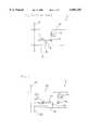
- An element driving device 1 illustrated by way of examplehas an organic EL element 2 as an active element and a power supply line 3 and a ground line 4 as a pair of power supply electrodes. A predetermined drive voltage is applied to power supply line 3, and ground line 4 is grounded.
- Organic EL element 2is connected directly to power while supply line 3 is connected to ground line 4 through TFT 5.
- TFT 5converts a drive voltage from power supply line 3 to be applied to ground line 4 into a drive current corresponding to a control voltage to be applied to a gate electrode to supply the current to organic EL element 2.
- the gate electrode of TFT 5is connected to holding capacitor 6 for holding a voltage, which is also connected to ground line 4. Holding capacitor 6 and the gate electrode of TFT 5 are connected to signal line 8 serving as a signal electrode through switching element 7. A control terminal of switching element 7 is connected to control line 9 serving as a control electrode.
- Holding capacitor 6holds the control voltage to apply the voltage to the gate electrode of TFT 5.
- Switching element 7turns on and off the connection between holding capacitor 6 and signal line 8.
- Signal line 8is supplied with the control voltage for driving the emission brightness of organic EL element 2.
- Control line 9is applied with a control signal for controlling the operation of switching element 7.
- Element driving device 1with the aforementioned the structure is capable of controlling organic EL element 2 at variable emission brightness, in such a way as to apply a control signal to control line 9 to turn on switching element 7, and with this state maintained, to supply a control voltage corresponding to the emission luminescence of organic EL element 2 from signal line 8 to holding capacitor 6 to hold the voltage.
- control voltage held in holding capacitor 6is applied to the gate electrode of TFT 5, causing TFT 5 to convert the drive voltage constantly applied to power supply line 3 to the drive current corresponding to the voltage at the gate to be supplied to organic EL element 2. This operation continues even after switching element 7 has been turned off with the control signal applied to control line 9.
- the drive current which is converted by TFT 5 from the drive voltage to be applied to power supply line 3 and supplied to organic EL element 2corresponds to the voltage to be applied from holding capacitor 6 to the gate electrode of TFT 5. Therefore, organic EL element 2 may emit light at brightness corresponding to the control voltage supplied on signal line 8.
- the aforementioned element driving device 1is intended to be utilized actually as an image display device.
- (m ⁇ n) organic EL elements 2are arranged in m rows and n columns, m signal lines 8 and n control lines 9 are applied with the control voltage and the control signal respectively in matrix form, to make (m ⁇ n) holding capacitors 6 to individually hold the control voltages.
- TFT 5can generate the drive current to be supplied variably to organic EL elements 2 from the drive voltage to be supplied to power supply line 3.
- the drive current to be generated by TFT 5 from the drive voltagecan be controlled with the voltage held in holding capacitor 6 which in turn can be controlled with the control voltage supplied to control line 8.
- each of m signal lines 8may be connected to n of (m ⁇ n) organic EL elements 2.
- the drive voltage to be supplied to organic EL element 2would be varied due to a voltage drop on signal line 8.
- organic EL elements 2 in element driving device 1are unable to emit light at the desired brightness, which results in deterioration of the quality of a displayed image with gradation obtained by an image display device using element driving device 1.
- an element driving devicewhich includes a first and second switching means and a voltage holding means.
- first and second switching meansWhen the first and second switching means are turned on with a control signal applied to a control electrode, a control current applied from a signal electrode through the second switching means is converted to a control voltage through a conversion transistor, which is held in the voltage holding means through the first switching means.
- a drive transistorconverts a drive voltage to be applied to a power supply electrode into a drive current, in correspondence to the control voltage held in the voltage holding means and then applied to a gate electrode, so that the operation of an active element supplied with the drive current is controlled in correspondence with the control current applied to the signal electrode. This operation continues through the voltage holding of the voltage holding means after the first and second switching means have been turned off.
- the signal electrodeis applied not with the control voltage, but with the control current. Therefore even in a structure in which multiple active elements may be connected to one signal electrode, no operational difference occurs in active elements due to a voltage drop.
- the drive transistor and a conversion transistormake up a current mirror circuit. For this reason, even when the drive transistor does not exhibit a desired operational characteristic due to a manufacturing error thereof, the drive current converted from the drive voltage through the drive transistor corresponds to the control current supplied to the conversion transistor if the conversion transistor has equivalently varied operational characteristics due to a similar manufacturing error, so that the active element will be supplied with the drive current corresponding to the control current on the signal electrode.
- the signal electrodeis applied with the control current, not with the control voltage, for controlling the operation of the active element, so that even in a structure in which multiple active elements are connected to one signal electrode, an operational difference in active elements due to a voltage drop can be prevented. Since the drive current corresponding to the control current on the signal electrode can be supplied to the active element, the active element can be controlled at a desired state.
- an element driving devicewhich includes a first and second switching means and a voltage holding means.
- first and second switching meansWhen the first and second switching means are turned on m by m with a control signal to be applied in turn to n control electrodes, n control currents applied in turn from m signal electrodes through the (m ⁇ n) second switching means to be turned on m by m are converted in turn into (m ⁇ n) control voltages through (m ⁇ n) conversion transistors.
- These (m ⁇ n) control voltagesare held in turn in (m ⁇ n) voltage holding means through the (m ⁇ n) first switching means to be turned on m by m.
- (m ⁇ n) drive transistorsindividually convert a drive voltage to be applied to a power supply electrode into drive currents, in correspondence to the control voltages individually held in the (m ⁇ n) voltage holding means, so that (m ⁇ n) active elements individually supplied with these (m ⁇ n) drive currents are controlled at correspondence to the control currents applied to the signal electrodes. This operation continues through the voltage holding of the voltage holding means after the first and second switching means have been turned off.
- the m signal electrodesare applied with the control current, not with the control voltage, for controlling the operation of the (m ⁇ n) active elements, so that even in a structure in which n of multiple (m ⁇ n) active elements are connected to each of m signal electrodes, no operational difference occurs in (m ⁇ n) active elements due to a voltage drop.
- the drive transistor and the conversion transistormake up a current mirror circuit. Therefore, even when the drive transistor does not exert a desired operational characteristic due to a manufacturing error, the drive current converted from the drive voltage through the drive transistor corresponds to the control current supplied to the conversion transistor if the conversion transistor has equivalently varied operational characteristics due to a similar manufacturing error, and the active element can be supplied with the drive current corresponding to the control current on the signal electrode.
- the signal electrodeis applied with the control current, not with the control voltage, for controlling the operation of the active element, so that an operational difference in multiple active elements due to a voltage drop on the signal electrode can be prevented.
- the drive current corresponding to the control current on the signal electrodecan be supplied to the active element, so that the active element can be controlled at a desired state.
- the conversion transistorneeds only to convert the control voltage into the control current. Therefore, the conversion transistor can be also replaced with a resistance element to simplify the structure.
- the resistance element and the drive transistordo not make up a current mirror circuit. Therefore, the accuracy of correspondence is reduced between the control current supplied from the signal electrode to the resistance element and the drive current converted from the drive voltage by the drive transistor. Nevertheless, the active element can be supplied with the drive current corresponding to the control current on the signal electrode and the drive current is not affected by a voltage drop when the signal electrode is applied with the control voltage.
- the conversion transistor forming a current mirror circuit together with the drive transistorcan be applied with the control voltage, not with the control current, from the signal electrode.
- the control voltage to be applied from the signal electrode to the conversion transistoris applied to the conversion transistor as a control current with its own electrical resistance, so that it is converted to the control voltage and held in the voltage holding means.
- the active elementmay be configured in the form of an organic EL element.
- the organic EL element serving as an active elementemits light at brightness corresponding to the control current applied to the signal electrode. Therefore, the organic EL element is allowed to emit light at desired brightness.
- each of the drive transistor and the conversion transistormay be a TFT and the TFTs of the drive transistor and the conversion transistor may be formed at positions close to each other on one circuit board. In this case, operational characteristics of the drive transistor and the conversion transistor are equivalently varied due to similar manufacturing errors.
- the drive current converted from the drive voltage through the drive transistormay correspond to the control current supplied to the conversion transistor, and the active element can be supplied with the drive current corresponding to the control current on the signal electrode.
- the active elementcan thus be accurately controlled at a desired state.
- the drive transistormay be connected in series to a first resistance element and the conversion transistor may be connected in series to a second resistance element.
- a ratio of a current change to a voltage variation in the drive transistoris reduced by the first resistance element connected thereto in series, and a ratio of a change in current for driving the active element to a variation in the drive voltage to be applied to the power supply electrode is reduced.
- the second resistance elementis connected to the conversion transistor similarly to the first resistance element. Operation as a current mirror circuit of the drive transistor and the conversion transistor may be favorable, so that the active element can be accurately controlled at a desired state.
- each of the first and second resistance elementsmay be configured as a TFT having its drain electrode and its gate electrode short-circuited.
- the TFTs of the first and second resistance elementsfunction as the resistance elements.
- the TFTs of these transistorscan be manufactured with the same processes as those of the TFTs of the first and second resistance elements. Productivity of the element driving device can thus be improved.
- the TFTs of the first resistance element and the second resistance elementmay be formed at positions close to each other on one circuit board.
- resistance characteristics of the first and second resistance elementsare equally varied due to similar manufacturing errors. Therefore, operation as a current mirror circuit of the drive transistor and the-conversion transistor is favorable.
- each of the first and second switching meansmay be configured as a TFT.
- the TFTs thereofcan be manufactured with the same processes as those of the TFTs of the first and second switching means. Productivity of the element driving device can thus be improved.
- an image display devicehaving the element driving devices according to the present invention and (m ⁇ n) active elements comprising display elements arranged in m rows and n columns. Therefore, in the image display device according to the present invention, the (m ⁇ n) active elements including the display elements arranged in m rows and n columns are driven in individually different display states by the element driving devices according to the present invention.
- the drive current satisfactorily corresponding to the control current on the signal electrodeis supplied to the active element, so that the image display device according to the present invention performs display operation with pixels having individually proper gradation levels. Therefore, an image in dot matrix which represents gradation in pixel unit can be displayed with favorable quality.
- an image display device with display elementscomprising (m ⁇ n) active elements arranged in m rows and n columns in the element driving devices according to the present invention.
- the (m ⁇ n) active elements in the element driving devices according to the present inventionare driven in individually different display states as the display elements arranged in m rows and n columns.
- the drive current satisfactorily corresponding to the control current on the signal electrodeis supplied to the active element, so that the image display device according to the present invention performs display operation with pixels having individually proper gradation levels. Therefore, an image in dot matrix which represents gradation in pixel unit can be displayed with favorable quality.
- FIG. 1is a circuit diagram showing an element driving device of one prior art
- FIG. 2is a circuit diagram showing an element driving device in a first embodiment according to the present invention
- FIG. 3is a plan view showing a thin-film structure of main units of the element driving device of the first embodiment
- FIG. 4is a block diagram showing an image display device in the first embodiment according to the present invention.
- FIG. 5is a circuit diagram showing a unit of a current driver of the image display device
- FIG. 6is a circuit diagram showing an element driving device of a first variation
- FIG. 7is a circuit diagram showing an element driving device of a second variation
- FIG. 8is a circuit diagram showing an element driving device of a second embodiment according to the present invention.
- FIG. 9is a circuit diagram showing an element driving device of a third variation.
- FIG. 10is a circuit diagram showing an element driving device of a fourth variation
- FIG. 11is a circuit diagram showing an element driving device of a fifth variation
- FIG. 12is a circuit diagram showing an element driving device of a sixth variation
- FIG. 13is a circuit diagram showing an element driving device of a seventh variation
- FIG. 14is a circuit diagram showing an element driving device of an eighth variation.
- FIG. 15is a circuit diagram showing an element driving device of a ninth variation.
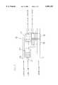
- a first embodiment according to the present inventionwill be hereinafter described with reference to FIG. 2 and FIG. 3.
- An element driving device (EDD) 11in the first embodiment according to the present invention.
- An element driving device (EDD) 11has an organic EL element 12 as an active element and a power supply line 13 and a ground line 14 as a pair of power supply electrodes, similarly to element driving device 1 of the prior art shown.
- Power supply line 13is applied with a predetermined drive voltage and ground line 14 is grounded.
- Organic EL element 12is connected directly to power supply line 13 and connected to ground line 14 through drive TFT 15 in the form of an n-channel MOS (Metal Oxide Semiconductor) FET (Field Effect Transistor) made of polysilicon.
- MOSMetal Oxide Semiconductor
- FETField Effect Transistor
- Drive TFT 15converts the drive voltage to be applied from power supply line 13 to ground line 14 into a drive current corresponding to a control voltage to be applied to a gate electrode and supplies the current to organic EL element 12.
- the gate electrode of drive TFT 15is connected to holding capacitor 16 for holding the voltage, which is also connected to ground line 14. Holding capacitor 16 and the gate electrode of drive TFT 15 are connected to one end of first switching element 17.
- conversion TFT 18which serves as a current converting element.
- Conversion TFT 18, as shown in FIG. 3,has the same structure as that of drive TFT 15 and is formed at a position close to drive TFT 15 on one circuit board 19.
- Conversion TFT 18is also connected to ground line 14 similarly to drive TFT 15. These TFTs 15, 18 make up a current mirror circuit through first switching element 17. Conversion TFT 18 is connected to signal line 21 serving as a signal electrode through second switching element 20. A control terminal of second switching element 20 is connected to control line 22 serving as a control electrode similarly to first switching element 17.
- each of first and second switching elements 17, 20also have a TFT of the similar structure to that of drive/conversion TFTs 15, 18, and formed at positions close to each other on circuit board 19.
- a control signal for controlling the emission brightness of organic EL element 12is supplied to signal line 21 as a variable control current, not as a variable control voltage.
- Control line 22is applied with a control signal for controlling the operation of first switching element 17 and second switching element 20.
- Second switching element 20turns on and off the connection between signal line 21 and conversion TFT 18.
- First switching element 17turns on and off the connection between conversion TFT 18 and holding capacitor 16.
- Conversion TFT 18converts the control current applied from signal line 21 through second switching element 20 into the control voltage.
- Holding capacitor 16holds the control voltage to be applied from conversion TFT 18 through first switching element 17 to apply the voltage to the gate electrode of drive TFT 15.
- Element driving device 11also constitutes actually a unit of image display device 1000 as shown in FIG. 4.
- image display device 1000 in this embodiment(m ⁇ n) organic EL elements 12 are arranged in m rows and n columns on circuit board 19.
- M signal lines 21are connected to one another to form collectively one set connected to one direct-current power supply 1001.
- M ground lines 14are connected to one another to form collectively one set connected to a large capacity component such as a housing (not shown) i.e., grounded.
- Each of m signal lines 21is connected individually to each of m current drivers 1002 for generating a control current.
- Each of n control lines 22is connected individually to each of n signal drivers 1003 for generating a control signal. All of drivers 1002, 1003 are connected to one integration control circuit (not shown), which controls the matrix drive of m current drives 1002 and n signal drivers 1003.
- Each of m current drivers 1002includes a voltage generation circuit 1004 and a current conversion circuit 1005 as shown in FIG. 5, which are connected to each other.
- Each of m voltage generation circuits 1004is connected to one direct-current power supply 1001 and the one integration control circuit.
- Each of m current conversion circuit 1005is connected to each of m signal lines 21.
- Each of voltage generation circuit 1004generates in turn voltages corresponding to the brightness of n organic EL elements 12 in each row from a constant-voltage generated by direct-current power supply 1001 under the control of the integration control circuit.
- Each of current conversion circuits 1005converts the voltage generated by voltage generation circuit 1004 to a signal current ranging from "0 to 2 ( ⁇ A)" to output the current to each of m signal lines 21.
- element driving device 11 in this embodimentsimilarly to element driving device 1 of one prior art, can control organic EL element 12 with variable emission brightness.
- the control signalis applied to control line 22 to turn on first and second switching elements 17, 20, and with this state, signal line 21 is applied with the control current corresponding to the emission brightness of organic EL element 12.
- control currentis then applied to conversion TFT 18 through second switching element 20 and converted to the control voltage.
- the control voltageis held in holding capacitor 16 through first switching element 17.
- the voltage held in holding capacitor 16is applied to the gate electrode of drive TFT 15. Accordingly, the drive voltage constantly applied to power supply line 13 is converted to the drive current through drive TFT 15 and supplied to organic EL element 12.
- the amount of the drive currentcorresponds to the voltage to be applied to the gate electrode of drive TFT 15 from holding capacitor 16.
- Organic EL element 12can thus emit light at brightness corresponding to the control current supplied to signal line 21. This operation is maintained by the voltage held in holding capacitor 16 even after first and second switching elements 17, 20 have been turned off.
- organic EL elements 12 arranged in matrixform emit light at individually controlled brightness. An image can thus be displayed in dot matrix which represents gradation in pixel unit.
- the control signal for controlling the emission brightness of organic EL element 12is applied to signal line 21 as the control current, not as the control voltage as discussed above. For this reason, even with a structure in which a number of organic EL elements 12 are connected to signal line 21 of microstructure for forming a high-definition image display device 1000, no difference occurs in the current for driving organic EL elements 12 due to a voltage drop applied to signal line 21.
- drive TFT 15 and conversion TFT 18make up a current mirror circuit. Therefore, even if drive TFT 15 fails to exhibit a desired operational characteristic due to a manufacturing error, the drive current to be converted from the drive voltage by drive TFT 15 corresponds to the control current to be supplied to conversion TFT 18 if the operational characteristic of conversion TFT 18 is equivalently varied due to a similar manufacturing error.
- element driving device 11it is possible to supply the drive current exactly corresponding to the control current conducted through signal line 21 to organic EL element 12. Therefore, image display device 1000 utilizing element driving device 11 according to this embodiment can display an image having gradation represented in pixel unit with good quality.
- drive/conversion TFTs 15 and 18which make up a current mirror circuit are formed at positions close to each other on circuit board 19. So that, drive/conversion TFTs 15, 18 can exhibit equivalent operational characteristics with similar manufacturing errors.
- first and second switching elements 17, 20are also configured as TFTs, so that first and second switching elements 17, 20 can be manufactured on the same processes as those of drive/conversion TFTs 15, 18. This eliminates incidentally dedicated processes for forming first and second switching elements 17, 20, thus improving productivity.
- the present embodimenthas been described as an example utilizing organic EL element 12 as an active element, the present invention is also applicable to various active elements such as an LED (Light Emitting Diode) and an LD (Laser Diode) which are controlled with a variable drive current.
- active elementssuch as an LED (Light Emitting Diode) and an LD (Laser Diode) which are controlled with a variable drive current.
- the present embodimenthas been shown as an example in which element driving devices 11 are arranged in matrix form to form image display device 1000, it is also possible to arrange the element driving devices in a line to form a line head of an electro-photograph device.
- the present embodimenthas been shown as an example in which element driving device 11 of microstructure is formed by use of a thin-film technology, the element driving device can also be assembled with a chip component in order to realize a very large image display device.
- element driving device 11includes organic EL element 12 which is an active element as a portion thereof
- organic EL element 12which is an active element as a portion thereof
- drive/conversion TFTs 15, 18are of n-channel structure and drive TFT 15 is formed in-between organic EL element 12 and ground line 14, it is also possible that drive/conversion TFTs 32, 33 are of p-channel structure and drive TFT 32 is formed in-between organic EL element 12 and power supply line 13, as with element driving device 31 illustrated in FIG. 6 as a first variation.
- TFTs 15, 18 of n-channel structurehave a substantially half occupied area as compared with TFTs 32, 33 of p-channel structure
- TFTs 15, 18 of n-channel structuremay preferably be employed to obtain a smaller and lighter device and a larger area available for organic EL element 12.
- the present embodimenthas been shown as an example in which it includes conversion TFT 18 which serves as a current conversion element for converting the control current to the control voltage, it is also possible to utilize resistance element 36 as the current conversion element, as with element driving device 35 illustrated in FIG. 7 as a second variation.
- resistance element 36 and drive TFT 15do not make up a current mirror circuit, the accuracy of correspondence between the control current and the drive current is lowered. Nevertheless, signal line 21 is supplied with the control current, not with the control voltage, so that a difference in emission brightness of organic EL elements 12 due to a voltage drop can be prevented.
- the present embodimenthas been shown as an example in which signal line 21 is supplied with the control current, not with the control voltage, if the control current is replaced with the control voltage, conversion/drive TFTs 15, 18 make up a current mirror circuit, so that the control voltage and the drive current can be made satisfactorily correspond to each other.
- control voltageis applied to conversion TFT 18 as the control current with its own electrical resistance.
- This control currentis converted to the control voltage by conversion TFT 18. Since conversion TFT 18 has an MOS resistance with a very small manufacturing error, a difference in the control current due to the manufacturing error of conversion TFT 18 is very small.
- the present embodimenthas been shown as an example in which holding capacitor 16 made of a single component as a member for holding the voltage and applying the voltage to the gate electrode of drive TFT 15, the gate electrode of drive TFT 15 may also hold the voltage with its own capacitance.
- drive TFT 15is connected in series to a first resistance element 42 and conversion TFT 18 is connected in series to second resistance element 43.
- the first and second resistance elements 42, 43may be made of, for example, a conductive thin-film, and have the same resistance value.
- element driving device 41functions similarly to element driving device 11 of the first embodiment. However, since in element driving device 41 according to this embodiment, drive TFT 15 is connected in series to first resistance element 42, a ratio of a current change to a voltage change in drive TFT 15 is reduced by means of first resistance element 42.
- element driving device 41In element driving device 41 according to this embodiment, a change in current for driving organic EL element 12 is thus reduced compared to a variation in drive voltage to be applied to power supply line 13. Therefore, organic EL element 12 is caused to favorably emit light at desired brightness, thus improving display quality when an image display device is formed.
- first and second resistance elements 42, 43are formed at positions close to each other on circuit board 19, a variation in resistance characteristics due to a manufacturing error of first and second resistance elements 42, 43 can be made equal to each other. Therefore, characteristic correction for drive/conversion TFTs 15, 18 by first and second resistance elements 42, 43 can be made equal to each other, and the current mirror circuit can thus be favorably operated.
- element driving device 51can be of course implemented such that the first and second resistance elements 42, 43 are connected to p-channel drive/conversion TFTs 32, 33, respectively.
- first and second resistance elements 62, 63may be configured as TFTs each having its drain electrode and its gate electrode short-circuited. In this case, each of these TFTs functions as a resistance element, so that element driving device 61 can function similarly to the element driving device 41.
- first and second resistance elements 62, 63 configured as TFTsmay be formed on the same processes as those of drive/conversion TFTs 15, 18, element driving device 61 has an improved productivity.
- first and second resistance elements 62, 63are also formed at positions close to each other on circuit board 19, a variation in resistance characteristics thereof due to a manufacturing error can be made equal to each other, so that a current mirror circuit consisting of drive/conversion TFTs 15, 18 can be operated satisfactorily.
- p-channel drive/conversion TFTs 32, 33may be connected to first and second resistance elements 72, 73 comprising p-channel TFTs.
- a drive transistorcan comprise a plurality of TFTs 15, to 15 3 connected in parallel, each of which being connected to a corresponding one of a plurality of first resistance elements 42 1 to 42 3 .
- drive TFTs 15 1 to 15 3 and conversion TFT 18 functioning as a current mirror circuithave a ratio of a conducting current "3:1". Therefore, a high drive current can be supplied to organic EL element 12 even with a very low control current.
- the drive transistorincludes the plurality of TFTs 15, to 15 3 connected in parallel for simplifying the description, they represent an equivalent circuit. Therefore, the plurality of TFTs 15 1 to 15 3 can be actually formed as one TFT which has an area three times larger than that of conversion TFT 18, and similarly, resistance elements 42 1 to 42 3 may be formed as one resistance element.
- the first and second resistance elementscan be omitted in a structure in which the current ratio in the current mirror circuit is set as described above.
- the current ratio in the current mirrorcan be set with p-channel drive/conversion TFTs 32 1 to 32 3 , and 33.
- first and second resistance elements 62 1 to 62 3 , and 63may be formed of TFTs in a structure in which a current ratio in a current mirror circuit is set.
- first and second resistance elements 72 1 to 72 3 , and 73may be formed of p-channel TFTs in a structure in which a current ratio in a current mirror circuit is set.
Landscapes
- Engineering & Computer Science (AREA)
- Physics & Mathematics (AREA)
- Computer Hardware Design (AREA)
- General Physics & Mathematics (AREA)
- Theoretical Computer Science (AREA)
- Control Of Indicators Other Than Cathode Ray Tubes (AREA)
- Control Of El Displays (AREA)
- Electroluminescent Light Sources (AREA)
Abstract
Description
Claims (25)
Applications Claiming Priority (2)
| Application Number | Priority Date | Filing Date | Title |
|---|---|---|---|
| JP10-086578 | 1998-03-31 | ||
| JP08657898AJP3252897B2 (en) | 1998-03-31 | 1998-03-31 | Element driving device and method, image display device |
Publications (1)
| Publication Number | Publication Date |
|---|---|
| US6091203Atrue US6091203A (en) | 2000-07-18 |
Family
ID=13890900
Family Applications (1)
| Application Number | Title | Priority Date | Filing Date |
|---|---|---|---|
| US09/275,889Expired - LifetimeUS6091203A (en) | 1998-03-31 | 1999-03-25 | Image display device with element driving device for matrix drive of multiple active elements |
Country Status (4)
| Country | Link |
|---|---|
| US (1) | US6091203A (en) |
| JP (1) | JP3252897B2 (en) |
| KR (1) | KR100291160B1 (en) |
| TW (1) | TW477156B (en) |
Cited By (230)
| Publication number | Priority date | Publication date | Assignee | Title |
|---|---|---|---|---|
| US6246180B1 (en)* | 1999-01-29 | 2001-06-12 | Nec Corporation | Organic el display device having an improved image quality |
| EP1170718A1 (en)* | 2000-07-07 | 2002-01-09 | Seiko Epson Corporation | Current sampling circuit for organic electroluminescent display |
| US20020005825A1 (en)* | 2000-07-15 | 2002-01-17 | Lee Han Sang | Electro-luminescence panel |
| US6373454B1 (en)* | 1998-06-12 | 2002-04-16 | U.S. Philips Corporation | Active matrix electroluminescent display devices |
| US20020047839A1 (en)* | 2000-09-20 | 2002-04-25 | Seiko Epson Corporation | Driving circuit for active matrix type display, drive method of electronic equipment and electronic apparatus, and electronic apparatus |
| US20020047581A1 (en)* | 2000-10-24 | 2002-04-25 | Jun Koyama | Light emitting device and method of driving the same |
| US20020047852A1 (en)* | 2000-09-04 | 2002-04-25 | Kazutaka Inukai | Method of driving EL display device |
| US20020053884A1 (en)* | 2000-11-07 | 2002-05-09 | Semiconductor Energy Laboratory Co., Ltd. | Light emitting device and electronic device |
| WO2002039420A1 (en) | 2000-11-07 | 2002-05-16 | Sony Corporation | Active matrix display and active matrix organic electroluminescence display |
| EP1132882A3 (en)* | 2000-03-06 | 2002-06-05 | Lg Electronics Inc. | Active driving circuit for display panel |
| EP1176579A3 (en)* | 2000-07-26 | 2002-06-19 | Lg Electronics Inc. | Current control circuit for display device |
| US20020113760A1 (en)* | 2001-02-21 | 2002-08-22 | Semiconductor Energy Laboratory Co., Ltd. | Light emitting device and electronic device |
| US20020118150A1 (en)* | 2000-12-29 | 2002-08-29 | Oh-Kyong Kwon | Organic electroluminescent display, driving method and pixel circuit thereof |
| US20020126073A1 (en)* | 1998-06-12 | 2002-09-12 | Philips Corporation | Active matrix electroluminescent display devices |
| US6479940B1 (en)* | 1999-09-17 | 2002-11-12 | Pioneer Corporation | Active matrix display apparatus |
| US20030001828A1 (en)* | 2001-05-31 | 2003-01-02 | Mitsuru Asano | Active matrix type display apparatus, active matrix type organic electroluminescence display apparatus, and driving methods thereof |
| US20030016191A1 (en)* | 2001-03-22 | 2003-01-23 | Canon Kabushiki Kaisha | Driving circuit of active matrix type light-emitting element |
| US20030025656A1 (en)* | 2001-08-03 | 2003-02-06 | Semiconductor Energy Laboratory Co., Ltd. | Display device and method of driving thereof |
| US20030030382A1 (en)* | 2001-08-10 | 2003-02-13 | Semiconductor Energy Laboratory Co., Ltd. | Display device and electronic equipment using the same |
| US6525704B1 (en)* | 1999-06-09 | 2003-02-25 | Nec Corporation | Image display device to control conduction to extend the life of organic EL elements |
| US20030043131A1 (en)* | 2001-09-05 | 2003-03-06 | Nec Corporation | Circuit for and method of driving current-driven device |
| US20030052843A1 (en)* | 2001-09-17 | 2003-03-20 | Shunpei Yamazaki | Light emitting device, method of driving a light emitting device, and electronic equipment |
| US20030062844A1 (en)* | 2001-09-10 | 2003-04-03 | Seiko Epson Corporation | Unit circuit, electronic circuit, electronic apparatus, electro-optic apparatus, driving method, and electronic equipment |
| WO2003027998A1 (en)* | 2001-09-25 | 2003-04-03 | Matsushita Electric Industrial Co., Ltd. | El display panel and el display apparatus comprising it |
| US20030062524A1 (en)* | 2001-08-29 | 2003-04-03 | Hajime Kimura | Light emitting device, method of driving a light emitting device, element substrate, and electronic equipment |
| US20030067455A1 (en)* | 2001-08-02 | 2003-04-10 | Seiko Epson Corporation | System and method for manufacturing an electro-optical device |
| US20030090447A1 (en)* | 2001-09-21 | 2003-05-15 | Hajime Kimura | Display device and driving method thereof |
| US20030107560A1 (en)* | 2001-01-15 | 2003-06-12 | Akira Yumoto | Active-matrix display, active-matrix organic electroluminescent display, and methods of driving them |
| US6580408B1 (en)* | 1999-06-03 | 2003-06-17 | Lg. Philips Lcd Co., Ltd. | Electro-luminescent display including a current mirror |
| US20030117352A1 (en)* | 2001-10-24 | 2003-06-26 | Hajime Kimura | Semiconductor device and driving method thereof |
| US20030128202A1 (en)* | 2002-01-09 | 2003-07-10 | Lg Electronics Inc. | Data drive circuit for current writing type amoel display panel |
| US20030128200A1 (en)* | 2000-11-07 | 2003-07-10 | Akira Yumoto | Active matrix display and active matrix organic electroluminescence display |
| GB2384100A (en)* | 2002-01-09 | 2003-07-16 | Seiko Epson Corp | A current driven element driving circuit |
| WO2002071379A3 (en)* | 2000-07-18 | 2003-07-17 | Emagin Corp | A current-type driver for organic light emitting diode displays |
| US20030137503A1 (en)* | 2002-01-24 | 2003-07-24 | Hajime Kimura | Semiconductor device and method of driving the semiconductor device |
| US20030156102A1 (en)* | 2001-10-30 | 2003-08-21 | Hajime Kimura | Signal line driving circuit, light emitting device, and method for driving the same |
| US20030164900A1 (en)* | 1999-08-26 | 2003-09-04 | Gilles Primeau | Sequential colour visual telepresence system |
| US20030169250A1 (en)* | 2001-10-30 | 2003-09-11 | Hajime Kimura | Signal line driver circuit, light emitting device and driving method thereof |
| US20030177915A1 (en)* | 2000-05-25 | 2003-09-25 | Jouko Kaki | Type of cationic starch product, preparation thereof and its use |
| EP1363264A2 (en) | 2002-05-17 | 2003-11-19 | Semiconductor Energy Laboratory Co., Ltd. | Current driven, light emitting active matrix display apparatus and driving method thereof |
| US20030214466A1 (en)* | 2002-05-17 | 2003-11-20 | Semiconductor Energy Laboratory Co., Ltd. | Display apparatus and driving method thereof |
| US20030218584A1 (en)* | 2002-05-17 | 2003-11-27 | Semiconductor Energy Laboratory Co., Ltd | Display device and driving method thereof |
| US6661180B2 (en) | 2001-03-22 | 2003-12-09 | Semiconductor Energy Laboratory Co., Ltd. | Light emitting device, driving method for the same and electronic apparatus |
| US20030227262A1 (en)* | 2002-06-11 | 2003-12-11 | Samsung Sdi Co., Ltd. | Light emitting display, light emitting display panel, and driving method thereof |
| US20040008166A1 (en)* | 2002-05-17 | 2004-01-15 | Semiconductor Energy Laboratory Co., Ltd. | Display device |
| US20040008072A1 (en)* | 2002-03-06 | 2004-01-15 | Hajime Kimura | Semiconductor integrated circuit and method of driving the same |
| US20040012550A1 (en)* | 2000-07-27 | 2004-01-22 | Semiconductor Energy Laboratory Co., Ltd. | Method of driving display device |
| US6693383B2 (en) | 2000-12-23 | 2004-02-17 | Lg.Philips Lcd Co., Ltd. | Electro-luminescence panel |
| US6693385B2 (en) | 2001-03-22 | 2004-02-17 | Semiconductor Energy Laboratory Co., Ltd. | Method of driving a display device |
| US20040041752A1 (en)* | 2002-05-17 | 2004-03-04 | Hajime Kimura | Display apparatus and driving method thereof |
| WO2004003877A3 (en)* | 2002-06-27 | 2004-04-22 | Casio Computer Co Ltd | Current drive apparatus and drive method thereof, and electroluminescent display apparatus using the circuit |
| WO2004034365A1 (en)* | 2002-10-08 | 2004-04-22 | Koninklijke Philips Electronics N.V. | Electroluminescent display devices |
| US20040080474A1 (en)* | 2001-10-26 | 2004-04-29 | Hajime Kimura | Light-emitting device and driving method thereof |
| US20040085270A1 (en)* | 2001-10-31 | 2004-05-06 | Hajime Kimura | Signal line driving circuit and light emitting device |
| US20040085029A1 (en)* | 2001-10-31 | 2004-05-06 | Hajime Kimura | Signal line driving circuit and light emitting device |
| US6738055B1 (en)* | 1999-03-24 | 2004-05-18 | Canon Kabushiki Kaisha | Flat-panel display apparatus and its control method |
| US20040095338A1 (en)* | 2002-08-30 | 2004-05-20 | Seiko Epson Corporation | Electronic circuit, method of driving electronic circuit, electro-optical device, method of driving electro-optical device, and electronic apparatus |
| US20040095298A1 (en)* | 2002-08-30 | 2004-05-20 | Seiko Epson Corporation | Electronic circuit, method of driving electronic circuit, electro-optical device, method of driving electro-optical device, and electronic apparatus |
| US20040095168A1 (en)* | 2002-10-03 | 2004-05-20 | Seiko Epson Corporation | Electronic circuit, method of driving electronic circuit, electronic device, electro-optical device, method of driving electro-optical device, and electronic apparatus |
| US20040100427A1 (en)* | 2002-08-07 | 2004-05-27 | Seiko Epson Corporation | Electronic circuit, electro-optical device, method for driving electro-optical device and electronic apparatus |
| US20040108998A1 (en)* | 2002-04-24 | 2004-06-10 | Seiko Epson Corporation | Electronic apparatus, electronic system, and driving method for electronic apparatus |
| US6753654B2 (en) | 2001-02-21 | 2004-06-22 | Semiconductor Energy Laboratory Co., Ltd. | Light emitting device and electronic appliance |
| US20040130262A1 (en)* | 2002-10-01 | 2004-07-08 | Sanyo Electric Co., Ltd. | Electroluminescent display device |
| US20040129933A1 (en)* | 2001-02-16 | 2004-07-08 | Arokia Nathan | Pixel current driver for organic light emitting diode displays |
| US20040135779A1 (en)* | 2003-01-07 | 2004-07-15 | Kazutaka Inukai | Circuit, display device, and electronic apparatus |
| US20040150350A1 (en)* | 2003-01-06 | 2004-08-05 | Kazutaka Inukai | Electronic circuit, display device, and electronic apparatus |
| US6774876B2 (en) | 2000-10-02 | 2004-08-10 | Semiconductor Energy Laboratory Co., Ltd. | Self light emitting device and driving method thereof |
| US6774877B2 (en) | 2001-06-25 | 2004-08-10 | Nec Corporation | Current driver circuit and image display device |
| US20040155873A1 (en)* | 2002-09-24 | 2004-08-12 | Seiko Epson Corporation | Electronic circuit, electro-optical device, method of driving electro-optical device, and electronic apparatus |
| US6777710B1 (en)* | 2001-02-26 | 2004-08-17 | Semiconductor Energy Laboratory Co., Ltd. | Organic light emitting device with constant luminance |
| US20040196218A1 (en)* | 2001-06-28 | 2004-10-07 | Kouji Senda | Active matrix el display and its driving method |
| US20040232952A1 (en)* | 2003-01-17 | 2004-11-25 | Hajime Kimura | Current source circuit, a signal line driver circuit and a driving method thereof and a light emitting device |
| US20040239379A1 (en)* | 2002-12-27 | 2004-12-02 | Kazutaka Inukai | Electronic circuit, electronic device and personal computer |
| US20040252084A1 (en)* | 2002-12-27 | 2004-12-16 | Keisuke Miyagawa | Semiconductor device, light-emitting display device and driving method thereof |
| US20040257356A1 (en)* | 2001-10-12 | 2004-12-23 | Semiconductor Energy Laboratory Co., Ltd., A Japan Corporation | Drive circuit, display device using the drive circuit and electronic apparatus using the display device |
| US20050012686A1 (en)* | 2003-03-26 | 2005-01-20 | Mitsuaki Osame | Element substrate and light-emitting device |
| US20050024303A1 (en)* | 2003-07-31 | 2005-02-03 | Semiconductor Energy Laboratory Co., Ltd. | Display device, a driving method of a display device, and a semiconductor integrated circuit incorporated in a display device |
| US20050041002A1 (en)* | 2001-09-07 | 2005-02-24 | Hiroshi Takahara | El display panel, its driving method, and el display apparatus |
| US20050145891A1 (en)* | 2002-01-17 | 2005-07-07 | Nec Corporation | Semiconductor device provided with matrix type current load driving circuits, and driving method thereof |
| US20050156917A1 (en)* | 2002-10-09 | 2005-07-21 | Youichi Tobita | Constant current circuit drive circuit and image display device |
| DE10360816A1 (en)* | 2003-12-23 | 2005-07-28 | Deutsche Thomson-Brandt Gmbh | Circuit and driving method for a light-emitting display |
| US20050174307A1 (en)* | 2002-08-02 | 2005-08-11 | Nec Corporation | Current drive circuit and image display device |
| US20050174419A1 (en)* | 2002-09-26 | 2005-08-11 | Seiko Epson Corporation | Image forming apparatus |
| US20050212740A1 (en)* | 2004-03-26 | 2005-09-29 | Semiconductor Energy Laboratory Co., Ltd. | Display device, driving method thereof, and electronic apparatus using the same |
| US20050224197A1 (en)* | 2004-04-12 | 2005-10-13 | Cheng Wen P | Combining device for tightly fixing screen to wall |
| US20050231123A1 (en)* | 2001-09-21 | 2005-10-20 | Semiconductor Energy Laboratory Co., Ltd., A Japan Corporation | Semiconductor device |
| US20050263718A1 (en)* | 2004-05-21 | 2005-12-01 | Seiko Epson Corporation | Line head and image forming apparatus incorporating the same |
| US20050272196A1 (en)* | 2004-05-31 | 2005-12-08 | Anelva Corporation | Method of depositing a higher permittivity dielectric film |
| US20060054893A1 (en)* | 2001-02-16 | 2006-03-16 | Arokia Nathan | Pixel driver circuit and pixel circuit having the pixel driver circuit |
| US20060063298A1 (en)* | 2004-09-20 | 2006-03-23 | Eastman Kodak Company | Providing driving current arrangement for oled device |
| US20060065812A1 (en)* | 2004-09-30 | 2006-03-30 | Seiko Epson Corporation | Line head and image forming apparatus |
| US20060097973A1 (en)* | 2004-10-28 | 2006-05-11 | Wein-Town Sun | Current-driven oled panel and related pixel structure |
| US20060119554A1 (en)* | 2004-12-06 | 2006-06-08 | Semiconductor Energy Laboratory Co., Ltd. | Display device, driving method thereof and electronic appliance |
| US20060139265A1 (en)* | 2004-12-28 | 2006-06-29 | Semiconductor Energy Laboratory Co., Ltd. | Driving method of display device |
| WO2006048801A3 (en)* | 2004-11-03 | 2006-07-06 | Koninkl Philips Electronics Nv | Electroluminescent display device |
| US20060220581A1 (en)* | 2001-09-21 | 2006-10-05 | Semiconductor Energy Laboratory Co., Ltd. | Light Emitting Device, Driving Method of Light Emitting Device and Electronic Device |
| US20060232600A1 (en)* | 2005-04-14 | 2006-10-19 | Semiconductor Energy Laboratory Co., Ltd. | Display device, driving method of the display device, and electronic device |
| US20060256047A1 (en)* | 1998-03-18 | 2006-11-16 | Seiko Epson Corporation | Transistor circuit, display panel and electronic apparatus |
| US20060261841A1 (en)* | 2004-08-20 | 2006-11-23 | Koninklijke Philips Electronics N.V. | Data signal driver for light emitting display |
| EP1732058A2 (en)* | 2001-01-04 | 2006-12-13 | International Business Machines Corporation | Low-power organic light emitting diode pixel circuit |
| US20060279260A1 (en)* | 2003-05-07 | 2006-12-14 | Toshiba Matsushita Display Technology Co., Ltd. | Current output type of semiconductor circuit, source driver for display drive, display device, and current output method |
| US20070008269A1 (en)* | 2000-04-26 | 2007-01-11 | Semiconductor Energy Laboratory Co., Ltd. | Electronic device and driving method thereof |
| US7180479B2 (en) | 2001-10-30 | 2007-02-20 | Semiconductor Energy Laboratory Co., Ltd. | Signal line drive circuit and light emitting device and driving method therefor |
| US20070046588A1 (en)* | 2005-08-30 | 2007-03-01 | Au Optronics Corp. | Acitvie display and pixel driving circuit thereof |
| US20070080905A1 (en)* | 2003-05-07 | 2007-04-12 | Toshiba Matsushita Display Technology Co., Ltd. | El display and its driving method |
| US20070120784A1 (en)* | 2002-04-26 | 2007-05-31 | Toshiba Matsushita Display Technology Co., Ltd | Semiconductor circuits for driving current-driven display and display |
| US20070126667A1 (en)* | 2005-12-01 | 2007-06-07 | Toshiba Matsushita Display Technology Co., Ltd. | El display apparatus and method for driving el display apparatus |
| US20070171241A1 (en)* | 2006-01-20 | 2007-07-26 | Semiconductor Energy Laboratory Co., Ltd. | Driving method of display device |
| US20070176538A1 (en)* | 2006-02-02 | 2007-08-02 | Eastman Kodak Company | Continuous conductor for OLED electrical drive circuitry |
| US20070182671A1 (en)* | 2003-09-23 | 2007-08-09 | Arokia Nathan | Pixel driver circuit |
| US20070200802A1 (en)* | 2002-09-26 | 2007-08-30 | Seiko Epson Corporation | Electronic circuit, electronic device, and electronic apparatus |
| US20070222718A1 (en)* | 2006-02-20 | 2007-09-27 | Toshiba Matsushita Display Technology Co., Ltd. | El display device and driving method of same |
| US20070273622A1 (en)* | 2006-05-29 | 2007-11-29 | Himax Technologies Limited | Amoled pixel unit |
| CN100354908C (en)* | 2002-09-25 | 2007-12-12 | 三星电子株式会社 | Organic luminous displaying device and manufacturing method thereof |
| CN100369092C (en)* | 2001-10-18 | 2008-02-13 | 三星电子株式会社 | Organic electroluminescent panel, display provided with the same, and apparatus and method for driving the same |
| CN100386794C (en)* | 2003-07-07 | 2008-05-07 | 三星Sdi株式会社 | Organic light emitting device pixel circuit and driving method thereof |
| US20080158112A1 (en)* | 2003-03-07 | 2008-07-03 | Canon Kabushiki Kaisha | Drive Circuit, Display Apparatus Using Drive Circuit, and Evaluation Method of Drive Circuit |
| US7405713B2 (en) | 2003-12-25 | 2008-07-29 | Semiconductor Energy Laboratory Co., Ltd. | Light emitting device and electronic equipment using the same |
| US20090117859A1 (en)* | 2006-04-07 | 2009-05-07 | Belair Networks Inc. | System and method for frequency offsetting of information communicated in mimo based wireless networks |
| US20090180466A1 (en)* | 2006-04-07 | 2009-07-16 | Belair Networks | System and method for frequency offsetting of information communicated in mimo-based wireless networks |
| US20090184900A1 (en)* | 2004-12-01 | 2009-07-23 | Philippe Le Roy | Image display device and display device control method |
| KR100923353B1 (en) | 2002-12-27 | 2009-10-22 | 엘지디스플레이 주식회사 | Electro-luminescence display and its driving method |
| US7623091B2 (en) | 2005-05-02 | 2009-11-24 | Semiconductor Energy Laboratory Co., Ltd. | Display device, and driving method and electronic apparatus of the display device |
| US20100001756A1 (en)* | 2004-10-25 | 2010-01-07 | Samsung Electronics Co., Ltd. | Array substrate having increased inspection efficincy and display apparatus having the same |
| US20100085283A1 (en)* | 2000-05-12 | 2010-04-08 | Semiconductor Energy Laboratory Co., Ltd. | Light-Emitting Device and Electric Appliance |
| US7719526B2 (en) | 2005-04-14 | 2010-05-18 | Semiconductor Energy Laboratory Co., Ltd. | Display device, and driving method and electronic apparatus of the display device |
| US7777698B2 (en) | 2002-04-26 | 2010-08-17 | Toshiba Matsushita Display Technology, Co., Ltd. | Drive method of EL display panel |
| US20110012883A1 (en)* | 2004-12-07 | 2011-01-20 | Ignis Innovation Inc. | Method and system for programming and driving active matrix light emitting device pixel |
| US20110124308A1 (en)* | 2006-04-07 | 2011-05-26 | Belair Networks Inc. | System and method for zero intermediate frequency filtering of information communicated in wireless networks |
| US8004200B2 (en) | 2003-03-26 | 2011-08-23 | Semiconductor Energy Laboratory Co., Ltd. | Element substrate and light emitting device |
| US8044893B2 (en) | 2005-01-28 | 2011-10-25 | Ignis Innovation Inc. | Voltage programmed pixel circuit, display system and driving method thereof |
| US20110317536A1 (en)* | 2010-06-24 | 2011-12-29 | Samsung Electro-Mechanics Co., Ltd. | Current driving circuit and light storage system having the same |
| CN101572056B (en)* | 2008-05-01 | 2012-07-04 | 索尼株式会社 | Diaplay apparatus and display-apparatus driving method |
| US8378935B2 (en) | 2005-01-14 | 2013-02-19 | Semiconductor Energy Laboratory Co., Ltd. | Display device having a plurality of subframes and method of driving the same |
| EP2660806A1 (en) | 2005-03-01 | 2013-11-06 | Global OLED Technology LLC | Oled display with improved active matrix circuitry |
| US8599191B2 (en) | 2011-05-20 | 2013-12-03 | Ignis Innovation Inc. | System and methods for extraction of threshold and mobility parameters in AMOLED displays |
| US8736524B2 (en) | 2004-12-15 | 2014-05-27 | Ignis Innovation, Inc. | Method and system for programming, calibrating and driving a light emitting device display |
| US8743096B2 (en) | 2006-04-19 | 2014-06-03 | Ignis Innovation, Inc. | Stable driving scheme for active matrix displays |
| US8803417B2 (en) | 2009-12-01 | 2014-08-12 | Ignis Innovation Inc. | High resolution pixel architecture |
| US8860636B2 (en) | 2005-06-08 | 2014-10-14 | Ignis Innovation Inc. | Method and system for driving a light emitting device display |
| US8901579B2 (en) | 2011-08-03 | 2014-12-02 | Ignis Innovation Inc. | Organic light emitting diode and method of manufacturing |
| US8907991B2 (en) | 2010-12-02 | 2014-12-09 | Ignis Innovation Inc. | System and methods for thermal compensation in AMOLED displays |
| USRE45291E1 (en) | 2004-06-29 | 2014-12-16 | Ignis Innovation Inc. | Voltage-programming scheme for current-driven AMOLED displays |
| US8922544B2 (en) | 2012-05-23 | 2014-12-30 | Ignis Innovation Inc. | Display systems with compensation for line propagation delay |
| US8994617B2 (en) | 2010-03-17 | 2015-03-31 | Ignis Innovation Inc. | Lifetime uniformity parameter extraction methods |
| US9030506B2 (en) | 2009-11-12 | 2015-05-12 | Ignis Innovation Inc. | Stable fast programming scheme for displays |
| US9058775B2 (en) | 2006-01-09 | 2015-06-16 | Ignis Innovation Inc. | Method and system for driving an active matrix display circuit |
| US9070775B2 (en) | 2011-08-03 | 2015-06-30 | Ignis Innovations Inc. | Thin film transistor |
| US9093029B2 (en) | 2011-05-20 | 2015-07-28 | Ignis Innovation Inc. | System and methods for extraction of threshold and mobility parameters in AMOLED displays |
| US9093028B2 (en) | 2009-12-06 | 2015-07-28 | Ignis Innovation Inc. | System and methods for power conservation for AMOLED pixel drivers |
| US9111485B2 (en) | 2009-06-16 | 2015-08-18 | Ignis Innovation Inc. | Compensation technique for color shift in displays |
| US9125278B2 (en) | 2006-08-15 | 2015-09-01 | Ignis Innovation Inc. | OLED luminance degradation compensation |
| US9134825B2 (en) | 2011-05-17 | 2015-09-15 | Ignis Innovation Inc. | Systems and methods for display systems with dynamic power control |
| US9171500B2 (en) | 2011-05-20 | 2015-10-27 | Ignis Innovation Inc. | System and methods for extraction of parasitic parameters in AMOLED displays |
| US9171504B2 (en) | 2013-01-14 | 2015-10-27 | Ignis Innovation Inc. | Driving scheme for emissive displays providing compensation for driving transistor variations |
| US9269322B2 (en) | 2006-01-09 | 2016-02-23 | Ignis Innovation Inc. | Method and system for driving an active matrix display circuit |
| US9275579B2 (en) | 2004-12-15 | 2016-03-01 | Ignis Innovation Inc. | System and methods for extraction of threshold and mobility parameters in AMOLED displays |
| US9280933B2 (en) | 2004-12-15 | 2016-03-08 | Ignis Innovation Inc. | System and methods for extraction of threshold and mobility parameters in AMOLED displays |
| US9305488B2 (en) | 2013-03-14 | 2016-04-05 | Ignis Innovation Inc. | Re-interpolation with edge detection for extracting an aging pattern for AMOLED displays |
| US9311859B2 (en) | 2009-11-30 | 2016-04-12 | Ignis Innovation Inc. | Resetting cycle for aging compensation in AMOLED displays |
| US9324268B2 (en) | 2013-03-15 | 2016-04-26 | Ignis Innovation Inc. | Amoled displays with multiple readout circuits |
| US9336717B2 (en) | 2012-12-11 | 2016-05-10 | Ignis Innovation Inc. | Pixel circuits for AMOLED displays |
| US9343006B2 (en) | 2012-02-03 | 2016-05-17 | Ignis Innovation Inc. | Driving system for active-matrix displays |
| US9351368B2 (en) | 2013-03-08 | 2016-05-24 | Ignis Innovation Inc. | Pixel circuits for AMOLED displays |
| US9370075B2 (en) | 2008-12-09 | 2016-06-14 | Ignis Innovation Inc. | System and method for fast compensation programming of pixels in a display |
| US9384698B2 (en) | 2009-11-30 | 2016-07-05 | Ignis Innovation Inc. | System and methods for aging compensation in AMOLED displays |
| US9385169B2 (en) | 2011-11-29 | 2016-07-05 | Ignis Innovation Inc. | Multi-functional active matrix organic light-emitting diode display |
| US9430958B2 (en) | 2010-02-04 | 2016-08-30 | Ignis Innovation Inc. | System and methods for extracting correlation curves for an organic light emitting device |
| US9437137B2 (en) | 2013-08-12 | 2016-09-06 | Ignis Innovation Inc. | Compensation accuracy |
| US9454931B2 (en) | 2005-12-08 | 2016-09-27 | Thomson Licensing | Luminous display and method for controlling the same |
| US9466240B2 (en) | 2011-05-26 | 2016-10-11 | Ignis Innovation Inc. | Adaptive feedback system for compensating for aging pixel areas with enhanced estimation speed |
| US9489891B2 (en) | 2006-01-09 | 2016-11-08 | Ignis Innovation Inc. | Method and system for driving an active matrix display circuit |
| US9502653B2 (en) | 2013-12-25 | 2016-11-22 | Ignis Innovation Inc. | Electrode contacts |
| US9530349B2 (en) | 2011-05-20 | 2016-12-27 | Ignis Innovations Inc. | Charged-based compensation and parameter extraction in AMOLED displays |
| US9606607B2 (en) | 2011-05-17 | 2017-03-28 | Ignis Innovation Inc. | Systems and methods for display systems with dynamic power control |
| US9697771B2 (en) | 2013-03-08 | 2017-07-04 | Ignis Innovation Inc. | Pixel circuits for AMOLED displays |
| US9721505B2 (en) | 2013-03-08 | 2017-08-01 | Ignis Innovation Inc. | Pixel circuits for AMOLED displays |
| US9741282B2 (en) | 2013-12-06 | 2017-08-22 | Ignis Innovation Inc. | OLED display system and method |
| US9747834B2 (en) | 2012-05-11 | 2017-08-29 | Ignis Innovation Inc. | Pixel circuits including feedback capacitors and reset capacitors, and display systems therefore |
| US9761170B2 (en) | 2013-12-06 | 2017-09-12 | Ignis Innovation Inc. | Correction for localized phenomena in an image array |
| US9773439B2 (en) | 2011-05-27 | 2017-09-26 | Ignis Innovation Inc. | Systems and methods for aging compensation in AMOLED displays |
| USRE46561E1 (en) | 2008-07-29 | 2017-09-26 | Ignis Innovation Inc. | Method and system for driving light emitting display |
| US9786223B2 (en) | 2012-12-11 | 2017-10-10 | Ignis Innovation Inc. | Pixel circuits for AMOLED displays |
| US9786209B2 (en) | 2009-11-30 | 2017-10-10 | Ignis Innovation Inc. | System and methods for aging compensation in AMOLED displays |
| WO2017177500A1 (en)* | 2016-04-12 | 2017-10-19 | 深圳市华星光电技术有限公司 | Amoled pixel driving circuit and pixel driving method |
| US9799246B2 (en) | 2011-05-20 | 2017-10-24 | Ignis Innovation Inc. | System and methods for extraction of threshold and mobility parameters in AMOLED displays |
| US9830857B2 (en) | 2013-01-14 | 2017-11-28 | Ignis Innovation Inc. | Cleaning common unwanted signals from pixel measurements in emissive displays |
| US9842889B2 (en) | 2014-11-28 | 2017-12-12 | Ignis Innovation Inc. | High pixel density array architecture |
| US9867257B2 (en) | 2008-04-18 | 2018-01-09 | Ignis Innovation Inc. | System and driving method for light emitting device display |
| US9881587B2 (en) | 2011-05-28 | 2018-01-30 | Ignis Innovation Inc. | Systems and methods for operating pixels in a display to mitigate image flicker |
| US9881532B2 (en) | 2010-02-04 | 2018-01-30 | Ignis Innovation Inc. | System and method for extracting correlation curves for an organic light emitting device |
| US9886899B2 (en) | 2011-05-17 | 2018-02-06 | Ignis Innovation Inc. | Pixel Circuits for AMOLED displays |
| US9947293B2 (en) | 2015-05-27 | 2018-04-17 | Ignis Innovation Inc. | Systems and methods of reduced memory bandwidth compensation |
| US9952698B2 (en) | 2013-03-15 | 2018-04-24 | Ignis Innovation Inc. | Dynamic adjustment of touch resolutions on an AMOLED display |
| CN108063905A (en)* | 2016-11-09 | 2018-05-22 | 京东方科技集团股份有限公司 | Pixel sensor circuit and its driving method, imaging sensor, electronic equipment |
| US10012678B2 (en) | 2004-12-15 | 2018-07-03 | Ignis Innovation Inc. | Method and system for programming, calibrating and/or compensating, and driving an LED display |
| US10013907B2 (en) | 2004-12-15 | 2018-07-03 | Ignis Innovation Inc. | Method and system for programming, calibrating and/or compensating, and driving an LED display |
| US10019941B2 (en) | 2005-09-13 | 2018-07-10 | Ignis Innovation Inc. | Compensation technique for luminance degradation in electro-luminance devices |
| US10074304B2 (en) | 2015-08-07 | 2018-09-11 | Ignis Innovation Inc. | Systems and methods of pixel calibration based on improved reference values |
| US10078984B2 (en) | 2005-02-10 | 2018-09-18 | Ignis Innovation Inc. | Driving circuit for current programmed organic light-emitting diode displays |
| US10089921B2 (en) | 2010-02-04 | 2018-10-02 | Ignis Innovation Inc. | System and methods for extracting correlation curves for an organic light emitting device |
| US10089924B2 (en) | 2011-11-29 | 2018-10-02 | Ignis Innovation Inc. | Structural and low-frequency non-uniformity compensation |
| US10102808B2 (en) | 2015-10-14 | 2018-10-16 | Ignis Innovation Inc. | Systems and methods of multiple color driving |
| US10134325B2 (en) | 2014-12-08 | 2018-11-20 | Ignis Innovation Inc. | Integrated display system |
| US10152915B2 (en) | 2015-04-01 | 2018-12-11 | Ignis Innovation Inc. | Systems and methods of display brightness adjustment |
| US10163996B2 (en) | 2003-02-24 | 2018-12-25 | Ignis Innovation Inc. | Pixel having an organic light emitting diode and method of fabricating the pixel |
| US10163401B2 (en) | 2010-02-04 | 2018-12-25 | Ignis Innovation Inc. | System and methods for extracting correlation curves for an organic light emitting device |
| US10176736B2 (en) | 2010-02-04 | 2019-01-08 | Ignis Innovation Inc. | System and methods for extracting correlation curves for an organic light emitting device |
| US10176752B2 (en) | 2014-03-24 | 2019-01-08 | Ignis Innovation Inc. | Integrated gate driver |
| US10181282B2 (en) | 2015-01-23 | 2019-01-15 | Ignis Innovation Inc. | Compensation for color variations in emissive devices |
| US10192479B2 (en) | 2014-04-08 | 2019-01-29 | Ignis Innovation Inc. | Display system using system level resources to calculate compensation parameters for a display module in a portable device |
| US10204540B2 (en) | 2015-10-26 | 2019-02-12 | Ignis Innovation Inc. | High density pixel pattern |
| US10235933B2 (en) | 2005-04-12 | 2019-03-19 | Ignis Innovation Inc. | System and method for compensation of non-uniformities in light emitting device displays |
| US10242619B2 (en) | 2013-03-08 | 2019-03-26 | Ignis Innovation Inc. | Pixel circuits for amoled displays |
| US10311780B2 (en) | 2015-05-04 | 2019-06-04 | Ignis Innovation Inc. | Systems and methods of optical feedback |
| US10319307B2 (en) | 2009-06-16 | 2019-06-11 | Ignis Innovation Inc. | Display system with compensation techniques and/or shared level resources |
| US10373554B2 (en) | 2015-07-24 | 2019-08-06 | Ignis Innovation Inc. | Pixels and reference circuits and timing techniques |
| US10410579B2 (en) | 2015-07-24 | 2019-09-10 | Ignis Innovation Inc. | Systems and methods of hybrid calibration of bias current |
| US10573231B2 (en) | 2010-02-04 | 2020-02-25 | Ignis Innovation Inc. | System and methods for extracting correlation curves for an organic light emitting device |
| US10586491B2 (en) | 2016-12-06 | 2020-03-10 | Ignis Innovation Inc. | Pixel circuits for mitigation of hysteresis |
| US10657895B2 (en) | 2015-07-24 | 2020-05-19 | Ignis Innovation Inc. | Pixels and reference circuits and timing techniques |
| US10714018B2 (en) | 2017-05-17 | 2020-07-14 | Ignis Innovation Inc. | System and method for loading image correction data for displays |
| US10867536B2 (en) | 2013-04-22 | 2020-12-15 | Ignis Innovation Inc. | Inspection system for OLED display panels |
| US10971078B2 (en) | 2018-02-12 | 2021-04-06 | Ignis Innovation Inc. | Pixel measurement through data line |
| US10997901B2 (en) | 2014-02-28 | 2021-05-04 | Ignis Innovation Inc. | Display system |
| US10996258B2 (en) | 2009-11-30 | 2021-05-04 | Ignis Innovation Inc. | Defect detection and correction of pixel circuits for AMOLED displays |
| US11025899B2 (en) | 2017-08-11 | 2021-06-01 | Ignis Innovation Inc. | Optical correction systems and methods for correcting non-uniformity of emissive display devices |
| US11302253B2 (en) | 2001-09-07 | 2022-04-12 | Joled Inc. | El display apparatus |
| US11699392B2 (en) | 2018-03-27 | 2023-07-11 | Sharp Kabushiki Kaisha | Display device |
| US20250131873A1 (en)* | 2022-06-23 | 2025-04-24 | Huawei Technologies Co., Ltd. | Display Circuit, Display Method, Display Apparatus, and Electronic Device |
Families Citing this family (56)
| Publication number | Priority date | Publication date | Assignee | Title |
|---|---|---|---|---|
| JP4049191B2 (en)* | 1999-06-17 | 2008-02-20 | ソニー株式会社 | Image display device |
| JP4049190B2 (en)* | 1999-06-17 | 2008-02-20 | ソニー株式会社 | Image display apparatus and driving method thereof |
| JP4079198B2 (en)* | 1999-06-17 | 2008-04-23 | ソニー株式会社 | Image display apparatus and driving method thereof |
| EP1130565A4 (en)* | 1999-07-14 | 2006-10-04 | Sony Corp | Current drive circuit and display comprising the same, pixel circuit, and drive method |
| US7379039B2 (en) | 1999-07-14 | 2008-05-27 | Sony Corporation | Current drive circuit and display device using same pixel circuit, and drive method |
| JP2001147659A (en)* | 1999-11-18 | 2001-05-29 | Sony Corp | Display device |
| JP2001166737A (en)* | 1999-12-10 | 2001-06-22 | Tdk Corp | Color picture display device |
| JP2001183996A (en)* | 1999-12-22 | 2001-07-06 | Tdk Corp | Image display device and driving method for thin film display element |
| KR100566813B1 (en)* | 2000-02-03 | 2006-04-03 | 엘지.필립스 엘시디 주식회사 | Electroluminescence cell driving circuit |
| TW531901B (en)* | 2000-04-27 | 2003-05-11 | Semiconductor Energy Lab | Light emitting device |
| JP4152603B2 (en)* | 2000-04-27 | 2008-09-17 | 株式会社半導体エネルギー研究所 | Light emitting device |
| JP5183838B2 (en)* | 2000-05-12 | 2013-04-17 | 株式会社半導体エネルギー研究所 | Light emitting device |
| WO2001091094A1 (en)* | 2000-05-22 | 2001-11-29 | Koninklijke Philips Electronics N.V. | Active matrix display device |
| TW493153B (en)* | 2000-05-22 | 2002-07-01 | Koninkl Philips Electronics Nv | Display device |
| JP3485175B2 (en) | 2000-08-10 | 2004-01-13 | 日本電気株式会社 | Electroluminescent display |
| JP4925528B2 (en)* | 2000-09-29 | 2012-04-25 | 三洋電機株式会社 | Display device |
| US6627907B1 (en)* | 2000-09-29 | 2003-09-30 | Honeywell International Inc. | Infrared scene projector with current-mirror control electronics |
| JP3594126B2 (en) | 2000-10-13 | 2004-11-24 | 日本電気株式会社 | Current drive circuit |
| TW550530B (en) | 2000-10-27 | 2003-09-01 | Semiconductor Energy Lab | Display device and method of driving the same |
| JP2002182612A (en)* | 2000-12-11 | 2002-06-26 | Sony Corp | Image display device |
| JP3950988B2 (en)* | 2000-12-15 | 2007-08-01 | エルジー フィリップス エルシーディー カンパニー リミテッド | Driving circuit for active matrix electroluminescent device |
| JP2002189445A (en)* | 2000-12-19 | 2002-07-05 | Sony Corp | Image display device and its driving method |
| JP4212815B2 (en)* | 2001-02-21 | 2009-01-21 | 株式会社半導体エネルギー研究所 | Light emitting device |
| JP2002287664A (en)* | 2001-03-23 | 2002-10-04 | Canon Inc | Display panel and its driving method |
| JP5070666B2 (en)* | 2001-08-24 | 2012-11-14 | パナソニック株式会社 | Pixel configuration and active matrix display device |
| US7209101B2 (en) | 2001-08-29 | 2007-04-24 | Nec Corporation | Current load device and method for driving the same |
| JP3656580B2 (en)* | 2001-08-29 | 2005-06-08 | 日本電気株式会社 | Light emitting element driving circuit and light emitting display device using the same |
| JP4742726B2 (en)* | 2001-09-10 | 2011-08-10 | セイコーエプソン株式会社 | Electronic device and electronic device |
| JP2010122700A (en)* | 2001-09-10 | 2010-06-03 | Seiko Epson Corp | Electro-optical device and electronic equipment |
| JP4581893B2 (en)* | 2001-09-10 | 2010-11-17 | セイコーエプソン株式会社 | Electronic device and electronic device |
| EP1428200A2 (en)* | 2001-09-20 | 2004-06-16 | Pioneer Corporation | Drive circuit for light emitting elements |
| JP2006338042A (en)* | 2001-09-21 | 2006-12-14 | Semiconductor Energy Lab Co Ltd | Light emitting device, and driving method of light emitting device |
| JP4540903B2 (en)* | 2001-10-03 | 2010-09-08 | パナソニック株式会社 | Active matrix display device |
| JP2003177709A (en) | 2001-12-13 | 2003-06-27 | Seiko Epson Corp | Pixel circuit for light emitting element |
| JP2003224437A (en)* | 2002-01-30 | 2003-08-08 | Sanyo Electric Co Ltd | Current drive circuit and display device equipped with the current drive circuit |
| JP4151882B2 (en)* | 2002-04-23 | 2008-09-17 | ローム株式会社 | Organic EL drive circuit and organic EL display device |
| KR20030086168A (en)* | 2002-05-03 | 2003-11-07 | 엘지.필립스 엘시디 주식회사 | The organic electro-luminescence device and method for fabricating of the same |
| JP3918642B2 (en)* | 2002-06-07 | 2007-05-23 | カシオ計算機株式会社 | Display device and driving method thereof |
| KR100441530B1 (en)* | 2002-06-11 | 2004-07-23 | 삼성에스디아이 주식회사 | Display device of organic electro luminescent and driving method there of |
| KR100489272B1 (en)* | 2002-07-08 | 2005-05-17 | 엘지.필립스 엘시디 주식회사 | Organic electroluminescence device and method for driving the same |
| JP3977299B2 (en)* | 2002-09-18 | 2007-09-19 | セイコーエプソン株式会社 | Electro-optical device, matrix substrate, and electronic apparatus |
| TW588468B (en)* | 2002-09-19 | 2004-05-21 | Ind Tech Res Inst | Pixel structure of active matrix organic light-emitting diode |
| KR100505370B1 (en)* | 2002-09-19 | 2005-08-03 | 재단법인서울대학교산학협력재단 | Pixel structure for active matrix organic light emitting diode display |
| TWI405156B (en) | 2003-01-06 | 2013-08-11 | Semiconductor Energy Lab | Circuit, display device, and electronic device |
| JP2006085199A (en)* | 2003-03-07 | 2006-03-30 | Canon Inc | Active matrix display device and drive control method thereof |
| JP4623939B2 (en)* | 2003-05-16 | 2011-02-02 | 株式会社半導体エネルギー研究所 | Display device |
| JP4547873B2 (en)* | 2003-06-16 | 2010-09-22 | ソニー株式会社 | Pixel circuit, display device, and driving method of pixel circuit |
| TWI241865B (en) | 2003-06-25 | 2005-10-11 | Rohm Co Ltd | Organic EL element drive circuit and organic EL display device using the same drive circuit |
| JP2005242323A (en)* | 2004-01-26 | 2005-09-08 | Semiconductor Energy Lab Co Ltd | Display device and its driving method |
| JP4976643B2 (en)* | 2004-03-19 | 2012-07-18 | 株式会社リコー | Active device, CMOS circuit using the same, and display device using the same |
| JP2005268618A (en)* | 2004-03-19 | 2005-09-29 | Ricoh Co Ltd | Active device, CMOS circuit using the same, and display device using the same |
| KR101127851B1 (en)* | 2005-06-30 | 2012-03-21 | 엘지디스플레이 주식회사 | A light emitting display device and a method for driving the same |
| JP5178861B2 (en)* | 2011-03-01 | 2013-04-10 | 株式会社半導体エネルギー研究所 | Display device |
| JP5712193B2 (en)* | 2012-11-22 | 2015-05-07 | 株式会社半導体エネルギー研究所 | Display device |
| KR102010803B1 (en) | 2017-12-29 | 2019-09-20 | 엘지디스플레이 주식회사 | Light emitting display device |
| CN111868815B (en)* | 2018-03-27 | 2022-07-26 | 夏普株式会社 | Display device |
Citations (12)
| Publication number | Priority date | Publication date | Assignee | Title |
|---|---|---|---|---|
| US4006383A (en)* | 1975-11-28 | 1977-02-01 | Westinghouse Electric Corporation | Electroluminescent display panel with enlarged active display areas |
| US4528480A (en)* | 1981-12-28 | 1985-07-09 | Nippon Telegraph & Telephone | AC Drive type electroluminescent display device |
| US4704559A (en)* | 1986-02-25 | 1987-11-03 | Seiko Instruments & Electronics Ltd. | Matrix type multi-color display device |
| US5153483A (en)* | 1990-04-12 | 1992-10-06 | Futaba Denshi Kogyo Kabushiki Kaisha | Display device |
| JPH0574569A (en)* | 1991-09-09 | 1993-03-26 | Fuji Xerox Co Ltd | Driving device of thin film el and its driving method |
| JPH0854835A (en)* | 1994-08-09 | 1996-02-27 | Nec Corp | Drive circuit for active matrix type current controlling light emitting element |
| US5552677A (en)* | 1995-05-01 | 1996-09-03 | Motorola | Method and control circuit precharging a plurality of columns prior to enabling a row of a display |
| US5684365A (en)* | 1994-12-14 | 1997-11-04 | Eastman Kodak Company | TFT-el display panel using organic electroluminescent media |
| US5767823A (en)* | 1995-10-05 | 1998-06-16 | Micron Display, Inc. | Method and apparatus for gray scale modulation of a matrix display |
| US5818406A (en)* | 1994-12-02 | 1998-10-06 | Nec Corporation | Driver circuit for liquid crystal display device |
| US5903248A (en)* | 1997-04-11 | 1999-05-11 | Spatialight, Inc. | Active matrix display having pixel driving circuits with integrated charge pumps |
| US5966110A (en)* | 1995-11-27 | 1999-10-12 | Stmicroelectronics S.A. | Led driver |
Family Cites Families (1)
| Publication number | Priority date | Publication date | Assignee | Title |
|---|---|---|---|---|
| US4996523A (en)* | 1988-10-20 | 1991-02-26 | Eastman Kodak Company | Electroluminescent storage display with improved intensity driver circuits |
- 1998
- 1998-03-31JPJP08657898Apatent/JP3252897B2/ennot_activeExpired - Lifetime
- 1999
- 1999-03-18TWTW088104224Apatent/TW477156B/ennot_activeIP Right Cessation
- 1999-03-25USUS09/275,889patent/US6091203A/ennot_activeExpired - Lifetime
- 1999-03-30KRKR1019990011092Apatent/KR100291160B1/ennot_activeExpired - Lifetime
Patent Citations (12)
| Publication number | Priority date | Publication date | Assignee | Title |
|---|---|---|---|---|
| US4006383A (en)* | 1975-11-28 | 1977-02-01 | Westinghouse Electric Corporation | Electroluminescent display panel with enlarged active display areas |
| US4528480A (en)* | 1981-12-28 | 1985-07-09 | Nippon Telegraph & Telephone | AC Drive type electroluminescent display device |
| US4704559A (en)* | 1986-02-25 | 1987-11-03 | Seiko Instruments & Electronics Ltd. | Matrix type multi-color display device |
| US5153483A (en)* | 1990-04-12 | 1992-10-06 | Futaba Denshi Kogyo Kabushiki Kaisha | Display device |
| JPH0574569A (en)* | 1991-09-09 | 1993-03-26 | Fuji Xerox Co Ltd | Driving device of thin film el and its driving method |
| JPH0854835A (en)* | 1994-08-09 | 1996-02-27 | Nec Corp | Drive circuit for active matrix type current controlling light emitting element |
| US5818406A (en)* | 1994-12-02 | 1998-10-06 | Nec Corporation | Driver circuit for liquid crystal display device |
| US5684365A (en)* | 1994-12-14 | 1997-11-04 | Eastman Kodak Company | TFT-el display panel using organic electroluminescent media |
| US5552677A (en)* | 1995-05-01 | 1996-09-03 | Motorola | Method and control circuit precharging a plurality of columns prior to enabling a row of a display |
| US5767823A (en)* | 1995-10-05 | 1998-06-16 | Micron Display, Inc. | Method and apparatus for gray scale modulation of a matrix display |
| US5966110A (en)* | 1995-11-27 | 1999-10-12 | Stmicroelectronics S.A. | Led driver |
| US5903248A (en)* | 1997-04-11 | 1999-05-11 | Spatialight, Inc. | Active matrix display having pixel driving circuits with integrated charge pumps |
Cited By (678)
| Publication number | Priority date | Publication date | Assignee | Title |
|---|---|---|---|---|
| US20060256047A1 (en)* | 1998-03-18 | 2006-11-16 | Seiko Epson Corporation | Transistor circuit, display panel and electronic apparatus |
| US7173584B2 (en) | 1998-03-18 | 2007-02-06 | Seiko Epson Corporation | Transistor circuit, display panel and electronic apparatus |
| US20110122124A1 (en)* | 1998-03-18 | 2011-05-26 | Seiko Epson Corporation | Transistor circuit, display panel and electronic apparatus |
| US8576144B2 (en) | 1998-03-18 | 2013-11-05 | Seiko Epson Corporation | Transistor circuit, display panel and electronic apparatus |
| US8593376B2 (en)* | 1998-06-12 | 2013-11-26 | Koninklijke Philips N.V. | Active matrix electroluminescent display devices |
| US20020126073A1 (en)* | 1998-06-12 | 2002-09-12 | Philips Corporation | Active matrix electroluminescent display devices |
| US6373454B1 (en)* | 1998-06-12 | 2002-04-16 | U.S. Philips Corporation | Active matrix electroluminescent display devices |
| US6246180B1 (en)* | 1999-01-29 | 2001-06-12 | Nec Corporation | Organic el display device having an improved image quality |
| US20040155875A1 (en)* | 1999-03-24 | 2004-08-12 | Canon Kabushiki Kaisha | Flat-panel display apparatus and its control method |
| US6738055B1 (en)* | 1999-03-24 | 2004-05-18 | Canon Kabushiki Kaisha | Flat-panel display apparatus and its control method |
| US7295197B2 (en) | 1999-03-24 | 2007-11-13 | Canon Kabushiki Kaisha | Flat-panel display apparatus and its control method |
| US6580408B1 (en)* | 1999-06-03 | 2003-06-17 | Lg. Philips Lcd Co., Ltd. | Electro-luminescent display including a current mirror |
| US6525704B1 (en)* | 1999-06-09 | 2003-02-25 | Nec Corporation | Image display device to control conduction to extend the life of organic EL elements |
| US20030164900A1 (en)* | 1999-08-26 | 2003-09-04 | Gilles Primeau | Sequential colour visual telepresence system |
| US6479940B1 (en)* | 1999-09-17 | 2002-11-12 | Pioneer Corporation | Active matrix display apparatus |
| EP1132882A3 (en)* | 2000-03-06 | 2002-06-05 | Lg Electronics Inc. | Active driving circuit for display panel |
| US6535185B2 (en) | 2000-03-06 | 2003-03-18 | Lg Electronics Inc. | Active driving circuit for display panel |
| US20070008269A1 (en)* | 2000-04-26 | 2007-01-11 | Semiconductor Energy Laboratory Co., Ltd. | Electronic device and driving method thereof |
| US20090309823A1 (en)* | 2000-04-26 | 2009-12-17 | Semiconductor Energy Laboratory Co., Ltd. | Electronic device and driving method thereof |
| US7557780B2 (en)* | 2000-04-26 | 2009-07-07 | Semiconductor Energy Laboratory Co., Ltd. | Electronic device and driving method thereof |
| US8514151B2 (en) | 2000-04-26 | 2013-08-20 | Semiconductor Energy Laboratory Co., Ltd. | Electronic device and driving method thereof |
| US8669925B2 (en) | 2000-05-12 | 2014-03-11 | Semiconductor Energy Laboratory Co., Ltd. | Light-emitting device and electric appliance |
| US20100085283A1 (en)* | 2000-05-12 | 2010-04-08 | Semiconductor Energy Laboratory Co., Ltd. | Light-Emitting Device and Electric Appliance |
| US8284138B2 (en) | 2000-05-12 | 2012-10-09 | Semiconductor Energy Laboratory Co., Ltd. | Light-emitting device and electric appliance |
| US20030177915A1 (en)* | 2000-05-25 | 2003-09-25 | Jouko Kaki | Type of cationic starch product, preparation thereof and its use |
| US20020033718A1 (en)* | 2000-07-07 | 2002-03-21 | Seiko Epson Corporation | Circuit, driver circuit, organic electroluminescent display device electro-optical device, electronic apparatus, method of controlling the current supply to an organic electroluminescent pixel, and method for driving a circuit |
| US6943759B2 (en) | 2000-07-07 | 2005-09-13 | Seiko Epson Corporation | Circuit, driver circuit, organic electroluminescent display device electro-optical device, electronic apparatus, method of controlling the current supply to an organic electroluminescent pixel, and method for driving a circuit |
| WO2002005254A1 (en)* | 2000-07-07 | 2002-01-17 | Seiko Epson Corporation | Current sampling circuit for organic electroluminescent display |
| EP1170718A1 (en)* | 2000-07-07 | 2002-01-09 | Seiko Epson Corporation | Current sampling circuit for organic electroluminescent display |
| US20050024298A1 (en)* | 2000-07-07 | 2005-02-03 | Seiko Epson Corporation | Circuit, driver circuit, organic electroluminescent display device electro-optical device, electronic apparatus, method of controlling the current supply to an organic electroluminescent pixel, and method for driving a circuit |
| US6744414B2 (en)* | 2000-07-15 | 2004-06-01 | Lg. Philips Lcd Co., Ltd. | Electro-luminescence panel |
| US20020005825A1 (en)* | 2000-07-15 | 2002-01-17 | Lee Han Sang | Electro-luminescence panel |
| WO2002071379A3 (en)* | 2000-07-18 | 2003-07-17 | Emagin Corp | A current-type driver for organic light emitting diode displays |
| EP1176579A3 (en)* | 2000-07-26 | 2002-06-19 | Lg Electronics Inc. | Current control circuit for display device |
| US6633136B2 (en)* | 2000-07-26 | 2003-10-14 | Lg Electronics Inc. | Current control circuit for display device of passive matrix type |
| US20040012550A1 (en)* | 2000-07-27 | 2004-01-22 | Semiconductor Energy Laboratory Co., Ltd. | Method of driving display device |
| US7158104B2 (en) | 2000-07-27 | 2007-01-02 | Semiconductor Energy Laboratory Co., Ltd. | Method of driving display device |
| US20070085783A1 (en)* | 2000-07-27 | 2007-04-19 | Semiconductor Energy Laboratory Co., Ltd. | Method of driving display device |
| US8508439B2 (en) | 2000-07-27 | 2013-08-13 | Semiconductor Energy Laboratory Co., Ltd. | Method of driving display device |
| US8035583B2 (en) | 2000-07-27 | 2011-10-11 | Semiconductor Energy Laboratory Co., Ltd. | Method of driving display device |
| US6879110B2 (en) | 2000-07-27 | 2005-04-12 | Semiconductor Energy Laboratory Co., Ltd. | Method of driving display device |
| US9489884B2 (en) | 2000-07-27 | 2016-11-08 | Semiconductor Energy Laboratory Co., Ltd. | Method of driving display device |
| US20020047852A1 (en)* | 2000-09-04 | 2002-04-25 | Kazutaka Inukai | Method of driving EL display device |
| WO2002021574A3 (en)* | 2000-09-04 | 2003-05-01 | Semiconductor Energy Lab | Subframe method for displaying grey scales on an active matrix el device with subdivided msb subframe |
| US7106290B2 (en) | 2000-09-04 | 2006-09-12 | Semiconductor Energy Laboratory Co., Ltd. | Method of driving EL display device |
| EP1184833A3 (en)* | 2000-09-04 | 2002-06-12 | Sel Semiconductor Energy Laboratory Co., Ltd. | Method of driving EL display device |
| CN100334607C (en)* | 2000-09-04 | 2007-08-29 | 株式会社半导体能源研究所 | Method for driving electroluminescent display device |
| US20020047839A1 (en)* | 2000-09-20 | 2002-04-25 | Seiko Epson Corporation | Driving circuit for active matrix type display, drive method of electronic equipment and electronic apparatus, and electronic apparatus |
| US6750833B2 (en)* | 2000-09-20 | 2004-06-15 | Seiko Epson Corporation | System and methods for providing a driving circuit for active matrix type displays |
| US7091939B2 (en) | 2000-09-20 | 2006-08-15 | Seiko Epson Corporation | System and methods for providing a driving circuit for active matrix type displays |
| US6774876B2 (en) | 2000-10-02 | 2004-08-10 | Semiconductor Energy Laboratory Co., Ltd. | Self light emitting device and driving method thereof |
| US20020047581A1 (en)* | 2000-10-24 | 2002-04-25 | Jun Koyama | Light emitting device and method of driving the same |
| US8558764B2 (en) | 2000-10-24 | 2013-10-15 | Semiconductor Energy Laboratory Co., Ltd. | Light emitting device and method of driving the same |
| US7317432B2 (en) | 2000-10-24 | 2008-01-08 | Semiconductor Energy Laboratory Co., Ltd. | Light emitting device and method of driving the same |
| CN1313996C (en)* | 2000-10-24 | 2007-05-02 | 株式会社半导体能源研究所 | Light emitting device |
| US7277070B2 (en) | 2000-10-24 | 2007-10-02 | Semiconductor Energy Laboratory Co. Ltd. | Light emitting device and method of driving the same |
| US20070236427A1 (en)* | 2000-10-24 | 2007-10-11 | Semiconductor Energy Laboratory Co., Ltd. | Light emitting device and method of driving the same |
| US20110090206A1 (en)* | 2000-11-07 | 2011-04-21 | Semiconductor Energy Laboratory Co., Ltd. | Light emitting device and electronic device |
| WO2002039420A1 (en) | 2000-11-07 | 2002-05-16 | Sony Corporation | Active matrix display and active matrix organic electroluminescence display |
| US7015882B2 (en)* | 2000-11-07 | 2006-03-21 | Sony Corporation | Active matrix display and active matrix organic electroluminescence display |
| US20020053884A1 (en)* | 2000-11-07 | 2002-05-09 | Semiconductor Energy Laboratory Co., Ltd. | Light emitting device and electronic device |
| US7030847B2 (en)* | 2000-11-07 | 2006-04-18 | Semiconductor Energy Laboratory Co., Ltd. | Light emitting device and electronic device |
| US9741289B2 (en) | 2000-11-07 | 2017-08-22 | Sony Corporation | Active-matrix display device, and active-matrix organic electroluminescent display device |
| US8558769B2 (en)* | 2000-11-07 | 2013-10-15 | Sony Corporation | Active-matrix display device, and active-matrix organic electroluminescent display device |
| US8711065B2 (en) | 2000-11-07 | 2014-04-29 | Semiconductor Energy Laboratory Co., Ltd. | Light emitting device and electronic device |
| US20060119552A1 (en)* | 2000-11-07 | 2006-06-08 | Akira Yumoto | Active-matrix display device, and active-matrix organic electroluminescent display device |
| EP1333422B1 (en)* | 2000-11-07 | 2013-05-22 | Sony Corporation | Active matrix display |
| US8810486B2 (en)* | 2000-11-07 | 2014-08-19 | Sony Corporation | Active-matrix display device, and active-matrix organic electroluminescent display device |
| US20030128200A1 (en)* | 2000-11-07 | 2003-07-10 | Akira Yumoto | Active matrix display and active matrix organic electroluminescence display |
| US8344972B2 (en) | 2000-11-07 | 2013-01-01 | Semiconductor Energy Laboratory Co., Ltd. | Light emitting device and electronic device |
| US20130088524A1 (en)* | 2000-11-07 | 2013-04-11 | Akira Yumoto | Active-matrix display device, and active-matrix organic electroluminescent display device |
| US20060192733A1 (en)* | 2000-11-07 | 2006-08-31 | Semiconductor Energy Laboratory Co., Ltd. | Light emitting device and electronic device |
| US8120551B2 (en)* | 2000-11-07 | 2012-02-21 | Sony Corporation | Active-matrix display device, and active-matrix organic electroluminescent display device |
| US10269296B2 (en) | 2000-11-07 | 2019-04-23 | Sony Corporation | Active-matrix display device, and active-matrix organic electroluminescent display device |
| US9245481B2 (en)* | 2000-11-07 | 2016-01-26 | Sony Corporation | Active-matrix display device, and active-matrix organic electroluminescent display device |
| US8139000B2 (en) | 2000-11-07 | 2012-03-20 | Semiconductor Energy Laboratory Co., Ltd. | Light emitting device and electronic device |
| US7817116B2 (en) | 2000-11-07 | 2010-10-19 | Semiconductor Energy Laboratory Co., Ltd. | Light emitting device and electronic device |
| US6693383B2 (en) | 2000-12-23 | 2004-02-17 | Lg.Philips Lcd Co., Ltd. | Electro-luminescence panel |
| EP1220191A3 (en)* | 2000-12-29 | 2003-09-10 | Samsung SDI Co., Ltd. | Organic electroluminescent display, driving method and pixel circuit thereof |
| US7015884B2 (en) | 2000-12-29 | 2006-03-21 | Samsung Sdi Co., Ltd. | Organic electroluminescent display, driving method and pixel circuit thereof |
| US20020118150A1 (en)* | 2000-12-29 | 2002-08-29 | Oh-Kyong Kwon | Organic electroluminescent display, driving method and pixel circuit thereof |
| EP1732058A2 (en)* | 2001-01-04 | 2006-12-13 | International Business Machines Corporation | Low-power organic light emitting diode pixel circuit |
| US20030107560A1 (en)* | 2001-01-15 | 2003-06-12 | Akira Yumoto | Active-matrix display, active-matrix organic electroluminescent display, and methods of driving them |
| US7019717B2 (en) | 2001-01-15 | 2006-03-28 | Sony Corporation | Active-matrix display, active-matrix organic electroluminescence display, and methods of driving them |
| US20060170624A1 (en)* | 2001-01-15 | 2006-08-03 | Sony Corporation | Active matrix type display device, active matrix type organic electroluminescent display device, and methods of driving such display devices |
| US7612745B2 (en) | 2001-01-15 | 2009-11-03 | Sony Corporation | Active matrix type display device, active matrix type organic electroluminescent display device, and methods of driving such display devices |
| US8890220B2 (en) | 2001-02-16 | 2014-11-18 | Ignis Innovation, Inc. | Pixel driver circuit and pixel circuit having control circuit coupled to supply voltage |
| US7569849B2 (en) | 2001-02-16 | 2009-08-04 | Ignis Innovation Inc. | Pixel driver circuit and pixel circuit having the pixel driver circuit |
| US20090284501A1 (en)* | 2001-02-16 | 2009-11-19 | Ignis Innovation Inc. | Pixel driver circuit and pixel circuit having the pixel driver circuit |
| US20060027807A1 (en)* | 2001-02-16 | 2006-02-09 | Arokia Nathan | Pixel current driver for organic light emitting diode displays |
| US20060054893A1 (en)* | 2001-02-16 | 2006-03-16 | Arokia Nathan | Pixel driver circuit and pixel circuit having the pixel driver circuit |
| US7414600B2 (en) | 2001-02-16 | 2008-08-19 | Ignis Innovation Inc. | Pixel current driver for organic light emitting diode displays |
| US20040129933A1 (en)* | 2001-02-16 | 2004-07-08 | Arokia Nathan | Pixel current driver for organic light emitting diode displays |
| US8664644B2 (en) | 2001-02-16 | 2014-03-04 | Ignis Innovation Inc. | Pixel driver circuit and pixel circuit having the pixel driver circuit |
| EP2180508A3 (en)* | 2001-02-16 | 2012-04-25 | Ignis Innovation Inc. | Pixel driver circuit for organic light emitting device |
| US8120557B2 (en) | 2001-02-21 | 2012-02-21 | Semiconductor Energy Laboratory Co., Ltd. | Light emitting device and electronic appliance |
| US20100201721A1 (en)* | 2001-02-21 | 2010-08-12 | Semiconductor Energy Laboratory Co., Ltd. | Light Emitting Device and Electronic Appliance |
| US20020113760A1 (en)* | 2001-02-21 | 2002-08-22 | Semiconductor Energy Laboratory Co., Ltd. | Light emitting device and electronic device |
| US7061451B2 (en)* | 2001-02-21 | 2006-06-13 | Semiconductor Energy Laboratory Co., Ltd, | Light emitting device and electronic device |
| US8780018B2 (en) | 2001-02-21 | 2014-07-15 | Semiconductor Energy Laboratory Co., Ltd. | Light emitting device and electronic appliance |
| US20080197777A1 (en)* | 2001-02-21 | 2008-08-21 | Semiconductor Energy Laboratory Co., Ltd. | Light emitting device and electronic appliance |
| US7336035B2 (en) | 2001-02-21 | 2008-02-26 | Semiconductor Energy Laboratory Co., Ltd. | Light emitting device and electronic appliance |
| US9040996B2 (en) | 2001-02-21 | 2015-05-26 | Semiconductor Energy Laboratory Co., Ltd. | Light emitting device and electronic appliance |
| US7719498B2 (en) | 2001-02-21 | 2010-05-18 | Semiconductor Energy Laboratory Co., Ltd. | Light emitting device and electronic appliance |
| US20040222749A1 (en)* | 2001-02-21 | 2004-11-11 | Semiconductor Energy Laboratory Co., Ltd. A Japan Corporation | Light emitting device and electronic appliance |
| US7612746B2 (en) | 2001-02-21 | 2009-11-03 | Semiconductor Energy Laboratory Co., Ltd. | Light emitting device and electronic device |
| US6753654B2 (en) | 2001-02-21 | 2004-06-22 | Semiconductor Energy Laboratory Co., Ltd. | Light emitting device and electronic appliance |
| US9431466B2 (en) | 2001-02-21 | 2016-08-30 | Semiconductor Energy Laboratory Co., Ltd. | Light emitting device and electronic appliance |
| US9886895B2 (en) | 2001-02-21 | 2018-02-06 | Semiconductor Energy Laboratory Co., Ltd. | Light emitting device and electronic appliance |
| US6777710B1 (en)* | 2001-02-26 | 2004-08-17 | Semiconductor Energy Laboratory Co., Ltd. | Organic light emitting device with constant luminance |
| US8610117B2 (en) | 2001-02-26 | 2013-12-17 | Semiconductor Energy Laboratory Co., Ltd. | Light emitting device and electronic equipment |
| US8071982B2 (en)* | 2001-02-26 | 2011-12-06 | Semiconductor Energy Laboratory Co., Ltd. | Light emitting device and electronic equipment |
| US20050002260A1 (en)* | 2001-02-26 | 2005-01-06 | Semiconductor Energy Laboratory Co., Ltd., A Japan Corporation | Light emitting device and electronic equipment |
| US20110084281A1 (en)* | 2001-02-26 | 2011-04-14 | Semiconductor Energy Laboratory Co., Ltd. | Light emitting device and electronic equipment |
| US7851796B2 (en) | 2001-02-26 | 2010-12-14 | Semiconductor Energy Laboratory Co., Ltd. | Light emitting device and electronic equipment |
| US8314427B2 (en) | 2001-02-26 | 2012-11-20 | Semiconductor Energy Laboratory Co., Ltd. | Light emitting device and electronic equipment |
| US20070007527A1 (en)* | 2001-03-22 | 2007-01-11 | Semiconductor Energy Laboratory Co., Ltd. | Light Emitting Device, Driving Method for the Same and Electronic Apparatus |
| US6914390B2 (en) | 2001-03-22 | 2005-07-05 | Semiconductor Energy Laboratory Co., Ltd. | Light emitting device, driving method for the same and electronic apparatus |
| US20080094327A1 (en)* | 2001-03-22 | 2008-04-24 | Semiconductor Energy Laboratory Co., Ltd. | Method of driving a display device |
| US20100006866A1 (en)* | 2001-03-22 | 2010-01-14 | Semiconductor Energy Laboratory Co., Ltd. | Light emitting device, driving method for the same and electronic apparatus |
| US6661180B2 (en) | 2001-03-22 | 2003-12-09 | Semiconductor Energy Laboratory Co., Ltd. | Light emitting device, driving method for the same and electronic apparatus |
| US20050007317A1 (en)* | 2001-03-22 | 2005-01-13 | Semiconductor Energy Laboratory Co., Ltd., A Japan Corporation | Method of driving a display device |
| US7283109B2 (en) | 2001-03-22 | 2007-10-16 | Semiconductor Energy Laboratory Co., Ltd. | Method of driving a display device |
| US20040100202A1 (en)* | 2001-03-22 | 2004-05-27 | Semiconductor Energy Laboratory Co., Ltd., A Japan Corporation | Light emitting device, driving method for the same and electronic apparatus |
| US6693385B2 (en) | 2001-03-22 | 2004-02-17 | Semiconductor Energy Laboratory Co., Ltd. | Method of driving a display device |
| US20030016191A1 (en)* | 2001-03-22 | 2003-01-23 | Canon Kabushiki Kaisha | Driving circuit of active matrix type light-emitting element |
| US6992663B2 (en)* | 2001-03-22 | 2006-01-31 | Canon Kabushiki Kaisha | Driving circuit of active matrix type light-emitting element |
| US7990350B2 (en) | 2001-03-22 | 2011-08-02 | Semiconductor Energy Laboratory Co., Ltd. | Light emitting device, driving method for the same and electronic apparatus |
| US8593066B2 (en) | 2001-03-22 | 2013-11-26 | Semiconductor Energy Laboratory Co., Ltd. | Light emitting device, driving method for same and electronic apparatus |
| US20050218400A1 (en)* | 2001-03-22 | 2005-10-06 | Semiconductor Energy Laboratory Co., Ltd., A Japan Corporation | Light emitting device, driving method for the same and electronic apparatus |
| US7106006B2 (en) | 2001-03-22 | 2006-09-12 | Semiconductor Energy Laboratory Co., Ltd. | Light emitting device, driving method for the same and electronic apparatus |
| US7952541B2 (en) | 2001-03-22 | 2011-05-31 | Semiconductor Energy Laboratory Co., Ltd. | Method of driving a display device |
| US7545353B2 (en) | 2001-03-22 | 2009-06-09 | Semiconductor Energy Laboratory Co., Ltd. | Light emitting device, driving method for the same and electronic apparatus |
| SG98054A1 (en)* | 2001-05-31 | 2003-08-20 | Sony Corp | Active matrix type display apparatus, active matrix type organic electroluminescence display apparatus, and driveing methods thereof |
| US6975290B2 (en) | 2001-05-31 | 2005-12-13 | Sony Corporation | Active matrix type display apparatus, active matrix type organic electroluminescence display apparatus, and driving methods thereof |
| US20030001828A1 (en)* | 2001-05-31 | 2003-01-02 | Mitsuru Asano | Active matrix type display apparatus, active matrix type organic electroluminescence display apparatus, and driving methods thereof |
| US6774877B2 (en) | 2001-06-25 | 2004-08-10 | Nec Corporation | Current driver circuit and image display device |
| US20040196218A1 (en)* | 2001-06-28 | 2004-10-07 | Kouji Senda | Active matrix el display and its driving method |
| US7061453B2 (en) | 2001-06-28 | 2006-06-13 | Matsushita Electric Industrial Co., Ltd. | Active matrix EL display device and method of driving the same |
| US7102600B2 (en) | 2001-08-02 | 2006-09-05 | Seiko Epson Corporation | System and method for manufacturing a electro-optical device |
| US20030067455A1 (en)* | 2001-08-02 | 2003-04-10 | Seiko Epson Corporation | System and method for manufacturing an electro-optical device |
| US7283111B2 (en) | 2001-08-03 | 2007-10-16 | Semiconductor Energy Laboratory Co., Ltd. | Display device and method of driving thereof |
| US20080117132A1 (en)* | 2001-08-03 | 2008-05-22 | Semiconductor Energy Laboratory Co., Ltd. | Display device and method of driving thereof |
| US8373625B2 (en) | 2001-08-03 | 2013-02-12 | Semiconductor Energy Laboratory Co., Ltd. | Display device and method of driving thereof |
| US20030025656A1 (en)* | 2001-08-03 | 2003-02-06 | Semiconductor Energy Laboratory Co., Ltd. | Display device and method of driving thereof |
| US20030030382A1 (en)* | 2001-08-10 | 2003-02-13 | Semiconductor Energy Laboratory Co., Ltd. | Display device and electronic equipment using the same |
| US7176859B2 (en) | 2001-08-10 | 2007-02-13 | Semiconductor Energy Laboratory Co., Ltd. | Display device and electronic equipment using the same |
| US8232937B2 (en) | 2001-08-10 | 2012-07-31 | Semiconductor Energy Laboratory Co., Ltd. | Display device and electronic equipment using the same |
| US20050099371A1 (en)* | 2001-08-10 | 2005-05-12 | Semiconductor Energy Laboratory Co., Ltd. | Display device and electronic equipment using the same |
| US20110074661A1 (en)* | 2001-08-10 | 2011-03-31 | Semiconductor Energy Laboratory Co., Ltd. | Display Device and Electronic Equipment Using the Same |
| US7804467B2 (en) | 2001-08-10 | 2010-09-28 | Semiconductor Energy Laboratory Co., Ltd. | Display device and electronic equipment using the same |
| US8749455B2 (en) | 2001-08-10 | 2014-06-10 | Semiconductor Energy Laboratory Co., Ltd. | Display device and electronic equipment using the same |
| US6876350B2 (en) | 2001-08-10 | 2005-04-05 | Semiconductor Energy Laboratory Co., Ltd. | Display device and electronic equipment using the same |
| US20070188421A1 (en)* | 2001-08-10 | 2007-08-16 | Semiconductor Energy Laboratory Co., Ltd. | Display device and electronic equipment using the same |
| US8482491B2 (en) | 2001-08-29 | 2013-07-09 | Semiconductor Energy Laboratory Co., Ltd. | Light emitting device, method of driving a light emitting device, element substrate, and electronic equipment |
| US7411586B2 (en) | 2001-08-29 | 2008-08-12 | Semiconductor Energy Laboratory Co., Ltd. | Light emitting device, method of driving a light emitting device, element substrate, and electronic equipment |
| US8982021B2 (en) | 2001-08-29 | 2015-03-17 | Semiconductor Energy Laboratory Co., Ltd. | Light emitting device, method of driving a light emitting device, element substrate, and electronic equipment |
| US8704736B2 (en) | 2001-08-29 | 2014-04-22 | Semiconductor Energy Laboratory Co., Ltd. | Light emitting device, method of driving a light emitting device, element substrate, and electronic equipment |
| US20030062524A1 (en)* | 2001-08-29 | 2003-04-03 | Hajime Kimura | Light emitting device, method of driving a light emitting device, element substrate, and electronic equipment |
| US7046240B2 (en) | 2001-08-29 | 2006-05-16 | Semiconductor Energy Laboratory Co., Ltd. | Light emitting device, method of driving a light emitting device, element substrate, and electronic equipment |
| US20060256046A1 (en)* | 2001-08-29 | 2006-11-16 | Semiconductor Energy Laboratory Co., Ltd. | Light Emitting Device, Method of Driving a Light Emitting Device, Element Substrate, and Electronic Equipment |
| US6839057B2 (en)* | 2001-09-05 | 2005-01-04 | Nec Corporation | Circuit for and method of driving current-driven device |
| US20030043131A1 (en)* | 2001-09-05 | 2003-03-06 | Nec Corporation | Circuit for and method of driving current-driven device |
| US9922597B2 (en) | 2001-09-07 | 2018-03-20 | Joled Inc. | EL display apparatus |
| US9959809B2 (en) | 2001-09-07 | 2018-05-01 | Joled Inc. | EL display apparatus |
| US10818235B2 (en) | 2001-09-07 | 2020-10-27 | Joled Inc. | EL display apparatus |
| US10134336B2 (en) | 2001-09-07 | 2018-11-20 | Joled Inc. | EL display apparatus |
| US8823606B2 (en)* | 2001-09-07 | 2014-09-02 | Panasonic Corporation | EL display panel, its driving method, and EL display apparatus |
| US11302253B2 (en) | 2001-09-07 | 2022-04-12 | Joled Inc. | El display apparatus |
| US9892683B2 (en) | 2001-09-07 | 2018-02-13 | Joled Inc. | EL display apparatus |
| US10923030B2 (en) | 2001-09-07 | 2021-02-16 | Joled Inc. | EL display apparatus |
| US10347183B2 (en) | 2001-09-07 | 2019-07-09 | Joled Inc. | EL display apparatus |
| US20050041002A1 (en)* | 2001-09-07 | 2005-02-24 | Hiroshi Takahara | El display panel, its driving method, and el display apparatus |
| US10453395B2 (en) | 2001-09-07 | 2019-10-22 | Joled Inc. | EL display apparatus |
| US10699639B2 (en) | 2001-09-07 | 2020-06-30 | Joled Inc. | EL display apparatus |
| US10198993B2 (en) | 2001-09-07 | 2019-02-05 | Joled Inc. | EL display apparatus |
| US10198992B2 (en) | 2001-09-07 | 2019-02-05 | Joled Inc. | EL display apparatus |
| US10553158B2 (en) | 2001-09-07 | 2020-02-04 | Joled Inc. | EL display apparatus |
| US9997108B1 (en) | 2001-09-07 | 2018-06-12 | Joled Inc. | EL display apparatus |
| US9728130B2 (en) | 2001-09-07 | 2017-08-08 | Joled Inc. | EL display apparatus |
| CN101373577B (en)* | 2001-09-10 | 2011-04-13 | 精工爱普生株式会社 | Electronic apparatus of drive current type driven element |
| EP1622121A3 (en)* | 2001-09-10 | 2007-06-20 | Seiko Epson Corporation | Unit circuit, electronic circuit, electronic apparatus, electro-optic apparatus, driving method and electronic equipment |
| EP1291841A3 (en)* | 2001-09-10 | 2004-04-28 | Seiko Epson Corporation | Unit circuit, electronic circuit, electronic apparatus, electro-optic apparatus, driving method, and electronic equipment |
| US20050116907A1 (en)* | 2001-09-10 | 2005-06-02 | Seiko Epson Corporation | Unit circuit, electronic circuit, electronic apparatus, electro-optic apparatus, driving method, and electronic equipment |
| KR100476131B1 (en)* | 2001-09-10 | 2005-03-15 | 세이코 엡슨 가부시키가이샤 | Unit circuit, electronic circuit, electronic device, electro optic device, driving method and electronic equipment |
| US20030062844A1 (en)* | 2001-09-10 | 2003-04-03 | Seiko Epson Corporation | Unit circuit, electronic circuit, electronic apparatus, electro-optic apparatus, driving method, and electronic equipment |
| US6858991B2 (en) | 2001-09-10 | 2005-02-22 | Seiko Epson Corporation | Unit circuit, electronic circuit, electronic apparatus, electro-optic apparatus, driving method, and electronic equipment |
| US7760162B2 (en) | 2001-09-10 | 2010-07-20 | Seiko Epson Corporation | Unit circuit, electronic circuit, electronic apparatus, electro-optic apparatus, driving method, and electronic equipment which can compensate for variations in characteristics of transistors to drive current-type driven elements |
| US20030052843A1 (en)* | 2001-09-17 | 2003-03-20 | Shunpei Yamazaki | Light emitting device, method of driving a light emitting device, and electronic equipment |
| US7250928B2 (en) | 2001-09-17 | 2007-07-31 | Semiconductor Energy Laboratory Co., Ltd. | Light emitting device, method of driving a light emitting device, and electronic equipment |
| US20030090447A1 (en)* | 2001-09-21 | 2003-05-15 | Hajime Kimura | Display device and driving method thereof |
| US7859520B2 (en) | 2001-09-21 | 2010-12-28 | Semiconductor Energy Laboratory Co., Ltd. | Display device and driving method thereof |
| KR100975775B1 (en)* | 2001-09-21 | 2010-08-17 | 가부시키가이샤 한도오따이 에네루기 켄큐쇼 | Semiconductor devices |
| US9165952B2 (en) | 2001-09-21 | 2015-10-20 | Semiconductor Energy Laboratory Co., Ltd. | Light emitting device, driving method of light emitting device and electronic device |
| CN102290005B (en)* | 2001-09-21 | 2017-06-20 | 株式会社半导体能源研究所 | The driving method of organic LED display device |
| US9876062B2 (en) | 2001-09-21 | 2018-01-23 | Semiconductor Energy Laboratory Co., Ltd. | Light emitting device, driving method of light emitting device and electronic device |
| US8227807B2 (en) | 2001-09-21 | 2012-07-24 | Semiconductor Energy Laboratory Co., Ltd. | Light emitting device, driving method of light emitting device and electronic device |
| US7915830B2 (en) | 2001-09-21 | 2011-03-29 | Semiconductor Energy Laboratory Co., Ltd. | Semiconductor device |
| US7795618B2 (en) | 2001-09-21 | 2010-09-14 | Semiconductor Energy Laboratory Co., Ltd. | Light emitting device, driving method of light emitting device and electronic device |
| US8895983B2 (en) | 2001-09-21 | 2014-11-25 | Semiconductor Energy Laboratory Co., Ltd. | Light emitting device, driving method of light emitting device and electronic device |
| US20100328299A1 (en)* | 2001-09-21 | 2010-12-30 | Semiconductor Energy Laboratory Co., Ltd. | Light emitting device, driving method of light emitting device and electronic device |
| US8604704B2 (en) | 2001-09-21 | 2013-12-10 | Semiconductor Energy Laboratory Co., Ltd. | Semiconductor device |
| US9368527B2 (en) | 2001-09-21 | 2016-06-14 | Semiconductor Energy Laboratory Co., Ltd. | Light emitting device, driving method of light emitting device and electronic device |
| US7138967B2 (en) | 2001-09-21 | 2006-11-21 | Semiconductor Energy Laboratory Co., Ltd. | Display device and driving method thereof |
| US10068953B2 (en) | 2001-09-21 | 2018-09-04 | Semiconductor Energy Laboratory Co., Ltd. | Light emitting device, driving method of light emitting device and electronic device |
| US9876063B2 (en) | 2001-09-21 | 2018-01-23 | Semiconductor Energy Laboratory Co., Ltd. | Light emitting device, driving method of light emitting device and electronic device |
| US20110169008A1 (en)* | 2001-09-21 | 2011-07-14 | Semiconductor Energy Laboratory Co., Ltd. | Semiconductor Device |
| US7170094B2 (en) | 2001-09-21 | 2007-01-30 | Semiconductor Energy Laboratory Co., Ltd. | Light emitting device, driving method of light emitting device and electronic device |
| US20050231123A1 (en)* | 2001-09-21 | 2005-10-20 | Semiconductor Energy Laboratory Co., Ltd., A Japan Corporation | Semiconductor device |
| US7583032B2 (en) | 2001-09-21 | 2009-09-01 | Semiconductor Energy Laboratory Co., Ltd. | Semiconductor device |
| US20100079177A1 (en)* | 2001-09-21 | 2010-04-01 | Semiconductor Energy Laboratory Co., Ltd. | Semiconductor device |
| US8378578B2 (en) | 2001-09-21 | 2013-02-19 | Semiconductor Energy Laboratory Co., Ltd. | Semiconductor device |
| EP1296310A3 (en)* | 2001-09-21 | 2005-10-26 | Sel Semiconductor Energy Laboratory Co., Ltd. | Semiconductor device for a TFTdisplay matrix |
| US8519392B2 (en) | 2001-09-21 | 2013-08-27 | Semiconductor Energy Laboratory Co., Ltd. | Light emitting device, driving method of light emitting device and electronic device |
| US20110134163A1 (en)* | 2001-09-21 | 2011-06-09 | Semiconductor Energy Laboratory Co., Ltd. | Display device and driving method thereof |
| US20070052635A1 (en)* | 2001-09-21 | 2007-03-08 | Semiconductor Energy Laboratory Co., Ltd. | Display device and driving method thereof |
| US20060220581A1 (en)* | 2001-09-21 | 2006-10-05 | Semiconductor Energy Laboratory Co., Ltd. | Light Emitting Device, Driving Method of Light Emitting Device and Electronic Device |
| US9847381B2 (en) | 2001-09-21 | 2017-12-19 | Semiconductor Energy Laboratory Co., Ltd. | Light emitting device, driving method of light emitting device and electronic device |
| US8599109B2 (en) | 2001-09-21 | 2013-12-03 | Semiconductor Energy Laboratory Co., Ltd. | Display device and driving method thereof |
| EP1296310B1 (en)* | 2001-09-21 | 2013-04-03 | Semiconductor Energy Laboratory Co., Ltd. | Semiconductor device for a TFTdisplay matrix |
| EP1450341A4 (en)* | 2001-09-25 | 2009-04-01 | Panasonic Corp | ELECTROLUMINESCENT SCREEN AND ELECTROLUMINESCENT DISPLAY DEVICE COMPRISING THE SAME |
| US20050057580A1 (en)* | 2001-09-25 | 2005-03-17 | Atsuhiro Yamano | El display panel and el display apparatus comprising it |
| WO2003027998A1 (en)* | 2001-09-25 | 2003-04-03 | Matsushita Electric Industrial Co., Ltd. | El display panel and el display apparatus comprising it |
| US7372437B2 (en) | 2001-10-12 | 2008-05-13 | Semiconductor Energy Laboratory Co., Ltd. | Drive circuit, display device using the drive circuit and electronic apparatus using the display device |
| US20040257356A1 (en)* | 2001-10-12 | 2004-12-23 | Semiconductor Energy Laboratory Co., Ltd., A Japan Corporation | Drive circuit, display device using the drive circuit and electronic apparatus using the display device |
| CN100369092C (en)* | 2001-10-18 | 2008-02-13 | 三星电子株式会社 | Organic electroluminescent panel, display provided with the same, and apparatus and method for driving the same |
| US20030117352A1 (en)* | 2001-10-24 | 2003-06-26 | Hajime Kimura | Semiconductor device and driving method thereof |
| US8378356B2 (en) | 2001-10-24 | 2013-02-19 | Semiconductor Energy Laboratory Co., Ltd. | Display device including pixel |
| US8659027B2 (en) | 2001-10-24 | 2014-02-25 | Semiconductor Energy Laboratory Co., Ltd. | Semiconductor device and electronic device |
| US9449549B2 (en) | 2001-10-24 | 2016-09-20 | Semiconductor Energy Laboratory Co., Ltd. | Semiconductor device and driving method thereof |
| US9892679B2 (en) | 2001-10-24 | 2018-02-13 | Semiconductor Energy Laboratory Co., Ltd. | Display device |
| US7365713B2 (en) | 2001-10-24 | 2008-04-29 | Semiconductor Energy Laboratory Co., Ltd. | Semiconductor device and driving method thereof |
| US8035109B2 (en) | 2001-10-24 | 2011-10-11 | Semiconductor Energy Laboratory Co., Ltd. | Display device including EL element |
| US8994029B2 (en) | 2001-10-24 | 2015-03-31 | Semiconductor Energy Laboratory Co., Ltd. | Semiconductor device and driving method thereof |
| US10679550B2 (en) | 2001-10-24 | 2020-06-09 | Semiconductor Energy Laboratory Co., Ltd. | Display device |
| US9082734B2 (en) | 2001-10-24 | 2015-07-14 | Semiconductor Energy Laboratory Co., Ltd. | Semiconductor device and driving method thereof |
| US20080284312A1 (en)* | 2001-10-24 | 2008-11-20 | Semiconductor Energy Laboratory Co., Ltd. | Semiconductor Device and Driving Method Thereof |
| US9171870B2 (en) | 2001-10-26 | 2015-10-27 | Semiconductor Energy Laboratory Co., Ltd. | Light-emitting device and driving method thereof |
| US20040080474A1 (en)* | 2001-10-26 | 2004-04-29 | Hajime Kimura | Light-emitting device and driving method thereof |
| US9601560B2 (en) | 2001-10-26 | 2017-03-21 | Semiconductor Energy Laboratory Co., Ltd. | Light-emitting device and driving method |
| US8941314B2 (en) | 2001-10-26 | 2015-01-27 | Semiconductor Energy Laboratory Co., Ltd. | Light-emitting device and driving method thereof |
| US7456810B2 (en)* | 2001-10-26 | 2008-11-25 | Semiconductor Energy Laboratory Co., Ltd. | Light-emitting device and driving method thereof |
| US10043862B2 (en) | 2001-10-26 | 2018-08-07 | Semiconductor Energy Laboratory Co., Ltd. | Light-emitting device and driving method thereof |
| US8063859B2 (en) | 2001-10-26 | 2011-11-22 | Semiconductor Energy Laboratory Co., Ltd. | Light-emitting device and driving method thereof |
| US20110205215A1 (en)* | 2001-10-26 | 2011-08-25 | Semiconductor Energy Laboratory Co., Ltd. | Light-Emitting Device and Driving Method Thereof |
| US20090096727A1 (en)* | 2001-10-26 | 2009-04-16 | Semiconductor Energy Laboratory Co., Ltd. | Light-emitting device and driving method thereof |
| US8305306B2 (en) | 2001-10-26 | 2012-11-06 | Semiconductor Energy Laboratory Co., Ltd. | Light-emitting device and driving method thereof |
| US20100253670A1 (en)* | 2001-10-30 | 2010-10-07 | Semiconductor Energy Laboratory Co., Ltd. | Signal line driver circuit, light emitting device and driving method thereof |
| US7180479B2 (en) | 2001-10-30 | 2007-02-20 | Semiconductor Energy Laboratory Co., Ltd. | Signal line drive circuit and light emitting device and driving method therefor |
| US8314754B2 (en) | 2001-10-30 | 2012-11-20 | Semiconductor Energy Laboratory Co., Ltd. | Signal line driver circuit, light emitting device and driving method thereof |
| US20090033649A1 (en)* | 2001-10-30 | 2009-02-05 | Semiconductor Energy Laboratory Co., Ltd. | Signal line driving circuit, light emitting device, and method for driving the same |
| CN101354863B (en)* | 2001-10-30 | 2011-01-19 | 株式会社半导体能源研究所 | Signal line drive circuit, light emitting device, and its drive method |
| CN100416636C (en)* | 2001-10-30 | 2008-09-03 | 株式会社半导体能源研究所 | Signal line driving circuit, light emitting device and driving method thereof |
| US8325165B2 (en) | 2001-10-30 | 2012-12-04 | Semiconductor Energy Laboratory Co., Ltd. | Signal line driving circuit, light emitting device, and method for driving the same |
| US7742064B2 (en) | 2001-10-30 | 2010-06-22 | Semiconductor Energy Laboratory Co., Ltd | Signal line driver circuit, light emitting device and driving method thereof |
| US8164548B2 (en) | 2001-10-30 | 2012-04-24 | Semiconductor Energy Laboratory Co., Ltd. | Signal line driver circuit and light emitting device and driving method therefor |
| CN100416635C (en)* | 2001-10-30 | 2008-09-03 | 株式会社半导体能源研究所 | Signal line driving circuit, light emitting device and driving method thereof |
| US7961159B2 (en) | 2001-10-30 | 2011-06-14 | Semiconductor Energy Laboratory Co., Ltd. | Signal line driver circuit, light emitting device and driving method thereof |
| US8624802B2 (en) | 2001-10-30 | 2014-01-07 | Semiconductor Energy Laboratory Co., Ltd. | Signal line driver circuit and light emitting device and driving method therefor |
| US20030169250A1 (en)* | 2001-10-30 | 2003-09-11 | Hajime Kimura | Signal line driver circuit, light emitting device and driving method thereof |
| US7576734B2 (en) | 2001-10-30 | 2009-08-18 | Semiconductor Energy Laboratory Co., Ltd. | Signal line driving circuit, light emitting device, and method for driving the same |
| CN101325030B (en)* | 2001-10-30 | 2011-07-06 | 株式会社半导体能源研究所 | Signal line driving circuit, light emitting device and driving method thereof |
| US20030156102A1 (en)* | 2001-10-30 | 2003-08-21 | Hajime Kimura | Signal line driving circuit, light emitting device, and method for driving the same |
| US7940235B2 (en) | 2001-10-31 | 2011-05-10 | Semiconductor Energy Laboratory Co., Ltd. | Signal line driving circuit and light emitting device |
| US20060103610A1 (en)* | 2001-10-31 | 2006-05-18 | Semiconductor Energy Laboratory Co., Ltd. | Signal line driving circuit and light emitting device |
| US7583257B2 (en) | 2001-10-31 | 2009-09-01 | Semiconductor Energy Laboratory Co., Ltd. | Signal line driving circuit and light emitting device |
| US20110012645A1 (en)* | 2001-10-31 | 2011-01-20 | Semiconductor Energy Laboratory Co., Ltd. | Signal line driving circuit and light emitting device |
| US8294640B2 (en) | 2001-10-31 | 2012-10-23 | Semiconductor Energy Laboratory Co., Ltd. | Signal line driving circuit and light emitting device |
| US6963336B2 (en) | 2001-10-31 | 2005-11-08 | Semiconductor Energy Laboratory Co., Ltd. | Signal line driving circuit and light emitting device |
| US20090303213A1 (en)* | 2001-10-31 | 2009-12-10 | Semiconductor Energy Laboratory Co., Ltd. | Signal line driving circuit and light emitting device |
| US7193619B2 (en) | 2001-10-31 | 2007-03-20 | Semiconductor Energy Laboratory Co., Ltd. | Signal line driving circuit and light emitting device |
| US8593377B2 (en) | 2001-10-31 | 2013-11-26 | Semiconductor Energy Laboratory Co., Ltd. | Signal line driving circuit and light emitting device |
| US20110234573A1 (en)* | 2001-10-31 | 2011-09-29 | Semiconductor Energy Laboratory Co., Ltd. | Signal line driving circuit and light emitting device |
| US9076385B2 (en) | 2001-10-31 | 2015-07-07 | Semiconductor Energy Laboratory Co., Ltd. | Signal line driving circuit and light emitting device |
| US20040085270A1 (en)* | 2001-10-31 | 2004-05-06 | Hajime Kimura | Signal line driving circuit and light emitting device |
| US7791566B2 (en) | 2001-10-31 | 2010-09-07 | Semiconductor Energy Laboratory Co., Ltd. | Signal line driving circuit and light emitting device |
| US20110205216A1 (en)* | 2001-10-31 | 2011-08-25 | Semiconductor Energy Laboratory Co., Ltd. | Signal line driving circuit and light emitting device |
| US7948453B2 (en) | 2001-10-31 | 2011-05-24 | Semiconductor Energy Laboratory Co., Ltd. | Signal line driving circuit and light emitting device |
| US20040085029A1 (en)* | 2001-10-31 | 2004-05-06 | Hajime Kimura | Signal line driving circuit and light emitting device |
| US20060028411A1 (en)* | 2002-01-09 | 2006-02-09 | Lg Electronics Inc. | Data drive circuit for current writing type AMOEL display panel |
| GB2384100A (en)* | 2002-01-09 | 2003-07-16 | Seiko Epson Corp | A current driven element driving circuit |
| US20030142046A1 (en)* | 2002-01-09 | 2003-07-31 | Seiko Epson Corporation | Electronic circuit, electroluminescent display device, electro-optical device, electronic apparatus, method of controlling the current supply to an organic electroluminescent pixel, and method for driving a circuit |
| GB2384100B (en)* | 2002-01-09 | 2005-10-26 | Seiko Epson Corp | An electronic circuit for controlling the current supply to an element |
| US20060208972A1 (en)* | 2002-01-09 | 2006-09-21 | Seiko Epson Corporation | Electronic circuit, electroluminescent display device, electro-optical device, electronic apparatus, method of controlling the current supply to an organic electroluminescent pixel, and method for driving a circuit |
| US7551151B2 (en) | 2002-01-09 | 2009-06-23 | Seiko Epson Corporation | Electronic circuit, electroluminescent display device, electro-optical device, electronic apparatus, method of controlling the current supply to an organic electroluminescent pixel, and method for driving a circuit |
| US7561125B2 (en) | 2002-01-09 | 2009-07-14 | Lg Display Co., Ltd. | Data drive circuit for current writing type AMOEL display panel |
| US7138968B2 (en)* | 2002-01-09 | 2006-11-21 | Seiko Epson Corporation | Electronic circuit, electroluminescent display device, electro-optical device, electronic apparatus, method of controlling the current supply to an organic electroluminescent pixel, and method for driving a circuit |
| US6982687B2 (en) | 2002-01-09 | 2006-01-03 | Lg Electronics Inc. | Data drive circuit for current writing type AMOEL display panel |
| US20030128202A1 (en)* | 2002-01-09 | 2003-07-10 | Lg Electronics Inc. | Data drive circuit for current writing type amoel display panel |
| EP1327972A3 (en)* | 2002-01-09 | 2004-07-14 | Lg Electronics Inc. | Data drive circuit for current writing type active matrix organic luminescent display panel |
| US7133012B2 (en) | 2002-01-17 | 2006-11-07 | Nec Corporation | Semiconductor device provided with matrix type current load driving circuits, and driving method thereof |
| US20050145891A1 (en)* | 2002-01-17 | 2005-07-07 | Nec Corporation | Semiconductor device provided with matrix type current load driving circuits, and driving method thereof |
| US7924244B2 (en) | 2002-01-24 | 2011-04-12 | Semiconductor Energy Laboratory Co., Ltd. | Semiconductor device and method of driving the semiconductor device |
| US8497823B2 (en) | 2002-01-24 | 2013-07-30 | Semiconductor Energy Laboratory Co., Ltd. | Semiconductor device and method of driving the semiconductor device |
| US8994622B2 (en) | 2002-01-24 | 2015-03-31 | Semiconductor Energy Laboratory Co., Ltd. | Semiconductor device and method of driving the semiconductor device |
| US20030137503A1 (en)* | 2002-01-24 | 2003-07-24 | Hajime Kimura | Semiconductor device and method of driving the semiconductor device |
| US11121203B2 (en) | 2002-01-24 | 2021-09-14 | Semiconductor Energy Laboratory Co., Ltd. | Semiconductor device and method of driving the semiconductor device |
| US9450036B2 (en) | 2002-01-24 | 2016-09-20 | Semiconductor Energy Laboratory Co., Ltd. | Semiconductor device and method of driving the semiconductor device |
| US10355068B2 (en) | 2002-01-24 | 2019-07-16 | Semiconductor Energy Laboratory Co., Ltd. | Semiconductor device and method of driving the semiconductor device |
| US20110115758A1 (en)* | 2002-01-24 | 2011-05-19 | Semiconductor Energy Laboratory Co., Ltd. | Semiconductor Device and Method of Driving the Semiconductor Device |
| US20100328288A1 (en)* | 2002-03-06 | 2010-12-30 | Semiconductor Energy Laboratory Co., Ltd. | Semiconductor integrated circuit and method of driving the same |
| US8373694B2 (en) | 2002-03-06 | 2013-02-12 | Semiconductor Energy Laboratory Co., Ltd. | Semiconductor integrated circuit and method of driving the same |
| US8004513B2 (en) | 2002-03-06 | 2011-08-23 | Semiconductor Energy Laboratory Co., Ltd. | Semiconductor integrated circuit and method of driving the same |
| US20040008072A1 (en)* | 2002-03-06 | 2004-01-15 | Hajime Kimura | Semiconductor integrated circuit and method of driving the same |
| US7728653B2 (en) | 2002-03-06 | 2010-06-01 | Semiconductor Energy Laboratory Co., Ltd. | Display and method of driving the same |
| US7310092B2 (en) | 2002-04-24 | 2007-12-18 | Seiko Epson Corporation | Electronic apparatus, electronic system, and driving method for electronic apparatus |
| US20040108998A1 (en)* | 2002-04-24 | 2004-06-10 | Seiko Epson Corporation | Electronic apparatus, electronic system, and driving method for electronic apparatus |
| US8194011B2 (en) | 2002-04-24 | 2012-06-05 | Seiko Epson Corporation | Electronic apparatus, electronic system, and driving method for electronic apparatus |
| US20070120784A1 (en)* | 2002-04-26 | 2007-05-31 | Toshiba Matsushita Display Technology Co., Ltd | Semiconductor circuits for driving current-driven display and display |
| US20100277401A1 (en)* | 2002-04-26 | 2010-11-04 | Toshiba Matsushita Display Technology Co., Ltd. | El display panel driving method |
| US7777698B2 (en) | 2002-04-26 | 2010-08-17 | Toshiba Matsushita Display Technology, Co., Ltd. | Drive method of EL display panel |
| US7932880B2 (en) | 2002-04-26 | 2011-04-26 | Toshiba Matsushita Display Technology Co., Ltd. | EL display panel driving method |
| US7817149B2 (en) | 2002-04-26 | 2010-10-19 | Toshiba Matsushita Display Technology Co., Ltd. | Semiconductor circuits for driving current-driven display and display |
| US20030214466A1 (en)* | 2002-05-17 | 2003-11-20 | Semiconductor Energy Laboratory Co., Ltd. | Display apparatus and driving method thereof |
| US7511687B2 (en) | 2002-05-17 | 2009-03-31 | Semiconductor Energy Laboratory Co., Ltd. | Display device, electronic apparatus and navigation system |
| CN100444217C (en)* | 2002-05-17 | 2008-12-17 | 株式会社半导体能源研究所 | Display device and driving method thereof |
| US7474285B2 (en) | 2002-05-17 | 2009-01-06 | Semiconductor Energy Laboratory Co., Ltd. | Display apparatus and driving method thereof |
| US7184034B2 (en) | 2002-05-17 | 2007-02-27 | Semiconductor Energy Laboratory Co., Ltd. | Display device |
| US20070103409A1 (en)* | 2002-05-17 | 2007-05-10 | Semiconductor Energy Laboratory Co., Ltd. | Display device and driving method thereof |
| US7864143B2 (en) | 2002-05-17 | 2011-01-04 | Semiconductor Energy Laboratory Co., Ltd. | Display device and driving method thereof |
| US20040008166A1 (en)* | 2002-05-17 | 2004-01-15 | Semiconductor Energy Laboratory Co., Ltd. | Display device |
| US7852297B2 (en) | 2002-05-17 | 2010-12-14 | Semiconductor Energy Laboratory Co., Ltd. | Display device |
| EP1363264A2 (en) | 2002-05-17 | 2003-11-19 | Semiconductor Energy Laboratory Co., Ltd. | Current driven, light emitting active matrix display apparatus and driving method thereof |
| US20030218584A1 (en)* | 2002-05-17 | 2003-11-27 | Semiconductor Energy Laboratory Co., Ltd | Display device and driving method thereof |
| EP1363264A3 (en)* | 2002-05-17 | 2010-06-23 | Semiconductor Energy Laboratory Co., Ltd. | Current driven, light emitting active matrix display apparatus and driving method thereof |
| US20030214465A1 (en)* | 2002-05-17 | 2003-11-20 | Semiconductor Energy Laboratory Co., Ltd. | Display apparatus and driving method thereof |
| US7532209B2 (en) | 2002-05-17 | 2009-05-12 | Semiconductor Energy Laboratory Co., Ltd. | Display apparatus and driving method thereof |
| US20040041752A1 (en)* | 2002-05-17 | 2004-03-04 | Hajime Kimura | Display apparatus and driving method thereof |
| US7170479B2 (en) | 2002-05-17 | 2007-01-30 | Semiconductor Energy Laboratory Co., Ltd. | Display device and driving method thereof |
| CN100403381C (en)* | 2002-05-17 | 2008-07-16 | 株式会社半导体能源研究所 | Display device and electronic equipment |
| US20030227262A1 (en)* | 2002-06-11 | 2003-12-11 | Samsung Sdi Co., Ltd. | Light emitting display, light emitting display panel, and driving method thereof |
| US7109952B2 (en)* | 2002-06-11 | 2006-09-19 | Samsung Sdi Co., Ltd. | Light emitting display, light emitting display panel, and driving method thereof |
| US20080174527A1 (en)* | 2002-06-27 | 2008-07-24 | Reiji Hattori | Current drive circuit and drive method thereof, and electroluminescent display apparatus using the circuit |
| WO2004003877A3 (en)* | 2002-06-27 | 2004-04-22 | Casio Computer Co Ltd | Current drive apparatus and drive method thereof, and electroluminescent display apparatus using the circuit |
| CN100590698C (en)* | 2002-06-27 | 2010-02-17 | 卡西欧计算机株式会社 | Current driving device, driving method thereof and display device using the same |
| CN101276540B (en)* | 2002-06-27 | 2010-09-01 | 卡西欧计算机株式会社 | Current drive circuit and drive method thereof, and electroluminescent display apparatus using the circuit |
| US8094095B2 (en) | 2002-06-27 | 2012-01-10 | Casio Computer Co., Ltd. | Current drive circuit and drive method thereof, and electroluminescent display apparatus using the circuit |
| US7173582B2 (en) | 2002-08-02 | 2007-02-06 | Nec Corporation | Current drive circuit and image display device |
| US20050174307A1 (en)* | 2002-08-02 | 2005-08-11 | Nec Corporation | Current drive circuit and image display device |
| US7589699B2 (en) | 2002-08-07 | 2009-09-15 | Seiko Epson Corporation | Electronic circuit, electro-optical device, method for driving electro-optical device and electronic apparatus |
| US20040100427A1 (en)* | 2002-08-07 | 2004-05-27 | Seiko Epson Corporation | Electronic circuit, electro-optical device, method for driving electro-optical device and electronic apparatus |
| US20060227083A1 (en)* | 2002-08-07 | 2006-10-12 | Seiko Epson Corporation | Electronic circuit, electro-optical device, method for driving electro-optical device and electronic apparatus |
| US7145530B2 (en) | 2002-08-07 | 2006-12-05 | Seiko Epson Corporation | Electronic circuit, electro-optical device, method for driving electro-optical device and electronic apparatus |
| US7158105B2 (en) | 2002-08-30 | 2007-01-02 | Seiko Epson Corporation | Electronic circuit, method of driving electronic circuit, electro-optical device, method of driving electro-optical device, and electronic apparatus |
| US20040095298A1 (en)* | 2002-08-30 | 2004-05-20 | Seiko Epson Corporation | Electronic circuit, method of driving electronic circuit, electro-optical device, method of driving electro-optical device, and electronic apparatus |
| US7786989B2 (en) | 2002-08-30 | 2010-08-31 | Seiko Epson Corporation | Electronic circuit, method of driving electronic circuit, electro-optical device, method of driving electro-optical device, and electronic apparatus |
| US20100123707A1 (en)* | 2002-08-30 | 2010-05-20 | Seiko Epson Corporation | Electronic Circuit, Method of Driving Electronic Circuit, Electro-Optical Device, Method of Driving Electro-Optical Device, and Electronic Apparatus |
| US7324101B2 (en) | 2002-08-30 | 2008-01-29 | Seiko Epson Corporation | Electronic circuit, method of driving electronic circuit, electro-optical device, method of driving electro-optical device, and electronic apparatus |
| US20040095338A1 (en)* | 2002-08-30 | 2004-05-20 | Seiko Epson Corporation | Electronic circuit, method of driving electronic circuit, electro-optical device, method of driving electro-optical device, and electronic apparatus |
| US7880690B2 (en) | 2002-08-30 | 2011-02-01 | Seiko Epson Corporation | Electronic circuit, method of driving electronic circuit, electro-optical device, method of driving electro-optical device, and electronic apparatus |
| US20060290617A1 (en)* | 2002-08-30 | 2006-12-28 | Seiko Epson Corporation | Electronic circuit, method of driving electronic circuit, electro-optical device, method of driving electro-optical device, and electronic apparatus |
| US20040155873A1 (en)* | 2002-09-24 | 2004-08-12 | Seiko Epson Corporation | Electronic circuit, electro-optical device, method of driving electro-optical device, and electronic apparatus |
| US7525520B2 (en) | 2002-09-24 | 2009-04-28 | Seiko Epson Corporation | Electronic circuit, electro-optical device, method of driving electro-optical device, and electronic apparatus |
| CN100354908C (en)* | 2002-09-25 | 2007-12-12 | 三星电子株式会社 | Organic luminous displaying device and manufacturing method thereof |
| US7417605B2 (en) | 2002-09-26 | 2008-08-26 | Seiko Epson Corporation | Electronic circuit, electronic device, and electronic apparatus |
| US20050174419A1 (en)* | 2002-09-26 | 2005-08-11 | Seiko Epson Corporation | Image forming apparatus |
| US7298350B2 (en)* | 2002-09-26 | 2007-11-20 | Seiko Epson Corporation | Image forming apparatus |
| US20070200802A1 (en)* | 2002-09-26 | 2007-08-30 | Seiko Epson Corporation | Electronic circuit, electronic device, and electronic apparatus |
| US20040130262A1 (en)* | 2002-10-01 | 2004-07-08 | Sanyo Electric Co., Ltd. | Electroluminescent display device |
| US6933756B2 (en) | 2002-10-03 | 2005-08-23 | Seiko Epson Corporation | Electronic circuit, method of driving electronic circuit, electronic device, electro-optical device, method of driving electro-optical device, and electronic apparatus |
| US20040095168A1 (en)* | 2002-10-03 | 2004-05-20 | Seiko Epson Corporation | Electronic circuit, method of driving electronic circuit, electronic device, electro-optical device, method of driving electro-optical device, and electronic apparatus |
| US7355459B2 (en) | 2002-10-03 | 2008-04-08 | Seiko Epson Corporation | Electronic circuit, method of driving electronic circuit, electronic device, electro-optical device, method of driving electro-optical device, and electronic apparatus |
| US20060261864A1 (en)* | 2002-10-03 | 2006-11-23 | Seiko Epson Corporation | Electronic circuit, method of driving electronic circuit, electronic device, electro-optical device, method of driving electro-optical device, and electronic apparatus |
| US7098705B2 (en) | 2002-10-03 | 2006-08-29 | Seiko Epson Corporation | Electronic circuit, method of driving electronic circuit, electronic device, electro-optical device, method of driving electro-optical device, and electronic apparatus |
| US20050218946A1 (en)* | 2002-10-03 | 2005-10-06 | Seiko Epson Corporation | Electronic circuit, method of driving electronic circuit, electronic device, electro-optical device, method of driving electro-optical device, and electronic apparatus |
| WO2004034365A1 (en)* | 2002-10-08 | 2004-04-22 | Koninklijke Philips Electronics N.V. | Electroluminescent display devices |
| US7317441B2 (en)* | 2002-10-09 | 2008-01-08 | Mitsubishi Denki Kabushiki Kaisha | Constant current circuit, drive circuit and image display device |
| US20050156917A1 (en)* | 2002-10-09 | 2005-07-21 | Youichi Tobita | Constant current circuit drive circuit and image display device |
| US20040239379A1 (en)* | 2002-12-27 | 2004-12-02 | Kazutaka Inukai | Electronic circuit, electronic device and personal computer |
| US7307604B2 (en) | 2002-12-27 | 2007-12-11 | Semiconductor Energy Laboratory Co., Ltd. | Semiconductor device, light-emitting display device and driving method thereof |
| KR100923353B1 (en) | 2002-12-27 | 2009-10-22 | 엘지디스플레이 주식회사 | Electro-luminescence display and its driving method |
| US7365715B2 (en) | 2002-12-27 | 2008-04-29 | Semiconductor Energy Laboratory Co., Ltd. | Electronic circuit, electronic device and personal computer |
| US20040252084A1 (en)* | 2002-12-27 | 2004-12-16 | Keisuke Miyagawa | Semiconductor device, light-emitting display device and driving method thereof |
| US7333099B2 (en) | 2003-01-06 | 2008-02-19 | Semiconductor Energy Laboratory Co., Ltd. | Electronic circuit, display device, and electronic apparatus |
| US20040150350A1 (en)* | 2003-01-06 | 2004-08-05 | Kazutaka Inukai | Electronic circuit, display device, and electronic apparatus |
| US20040135779A1 (en)* | 2003-01-07 | 2004-07-15 | Kazutaka Inukai | Circuit, display device, and electronic apparatus |
| US7348947B2 (en) | 2003-01-07 | 2008-03-25 | Semiconductor Energy Laboratory Co., Ltd. | Circuit, display device, and electronic apparatus |
| US9626913B2 (en) | 2003-01-17 | 2017-04-18 | Semiconductor Energy Laboratory Co., Ltd. | Current source circuit, a signal line driver circuit and a driving method thereof and a light emitting device |
| US8659529B2 (en)* | 2003-01-17 | 2014-02-25 | Semiconductor Energy Laboratory Co., Ltd. | Current source circuit, a signal line driver circuit and a driving method thereof and a light emitting device |
| US20040232952A1 (en)* | 2003-01-17 | 2004-11-25 | Hajime Kimura | Current source circuit, a signal line driver circuit and a driving method thereof and a light emitting device |
| US10163996B2 (en) | 2003-02-24 | 2018-12-25 | Ignis Innovation Inc. | Pixel having an organic light emitting diode and method of fabricating the pixel |
| US20080158112A1 (en)* | 2003-03-07 | 2008-07-03 | Canon Kabushiki Kaisha | Drive Circuit, Display Apparatus Using Drive Circuit, and Evaluation Method of Drive Circuit |
| US8159482B2 (en) | 2003-03-07 | 2012-04-17 | Canon Kabushiki Kaisha | Drive circuit, display apparatus using drive circuit, and evaluation method of drive circuit |
| US20080157828A1 (en)* | 2003-03-07 | 2008-07-03 | Canon Kabushiki Kaisha | Drive Circuit, Display Apparatus Using Drive Circuit, and Evaluation Method of Drive Circuit |
| US8154539B2 (en) | 2003-03-07 | 2012-04-10 | Canon Kabushiki Kaisha | Drive circuit, display apparatus using drive circuit, and evaluation method of drive circuit |
| US20050012686A1 (en)* | 2003-03-26 | 2005-01-20 | Mitsuaki Osame | Element substrate and light-emitting device |
| US9300771B2 (en) | 2003-03-26 | 2016-03-29 | Semiconductor Energy Laboratory Co., Ltd. | Element substrate and light-emitting device |
| US9698207B2 (en) | 2003-03-26 | 2017-07-04 | Semiconductor Energy Laboratory Co., Ltd. | Element substrate and light-emitting device |
| US8212488B2 (en) | 2003-03-26 | 2012-07-03 | Semiconductor Energy Laboratory Co., Ltd. | Element substrate and light emitting device |
| US8026877B2 (en) | 2003-03-26 | 2011-09-27 | Semiconductor Energy Laboratory Co., Ltd. | Element substrate and light-emitting device |
| US8659523B2 (en) | 2003-03-26 | 2014-02-25 | Semiconductor Energy Laboratory Co., Ltd. | Element substrate and light-emitting device |
| US8004200B2 (en) | 2003-03-26 | 2011-08-23 | Semiconductor Energy Laboratory Co., Ltd. | Element substrate and light emitting device |
| US9147720B2 (en) | 2003-03-26 | 2015-09-29 | Semiconductor Energy Laboratory Co., Ltd. | Element substrate and light emitting device |
| US8400067B2 (en) | 2003-03-26 | 2013-03-19 | Semiconductor Energy Laboratory Co., Ltd. | Element substrate and light emitting device |
| US11430845B2 (en) | 2003-03-26 | 2022-08-30 | Semiconductor Energy Laboratory Co., Ltd. | Element substrate and light-emitting device |
| US8759825B2 (en) | 2003-03-26 | 2014-06-24 | Semiconductor Energy Laboratory Co., Ltd. | Element substrate and light emitting device |
| US20070080905A1 (en)* | 2003-05-07 | 2007-04-12 | Toshiba Matsushita Display Technology Co., Ltd. | El display and its driving method |
| US20060279260A1 (en)* | 2003-05-07 | 2006-12-14 | Toshiba Matsushita Display Technology Co., Ltd. | Current output type of semiconductor circuit, source driver for display drive, display device, and current output method |
| US7561147B2 (en) | 2003-05-07 | 2009-07-14 | Toshiba Matsushita Display Technology Co., Ltd. | Current output type of semiconductor circuit, source driver for display drive, display device, and current output method |
| US7414599B2 (en) | 2003-07-07 | 2008-08-19 | Samsung Sdi Co., Ltd. | Organic light emitting device pixel circuit and driving method therefor |
| CN100386794C (en)* | 2003-07-07 | 2008-05-07 | 三星Sdi株式会社 | Organic light emitting device pixel circuit and driving method thereof |
| US7961160B2 (en) | 2003-07-31 | 2011-06-14 | Semiconductor Energy Laboratory Co., Ltd. | Display device, a driving method of a display device, and a semiconductor integrated circuit incorporated in a display device |
| US20050024303A1 (en)* | 2003-07-31 | 2005-02-03 | Semiconductor Energy Laboratory Co., Ltd. | Display device, a driving method of a display device, and a semiconductor integrated circuit incorporated in a display device |
| US20070182671A1 (en)* | 2003-09-23 | 2007-08-09 | Arokia Nathan | Pixel driver circuit |
| US10089929B2 (en) | 2003-09-23 | 2018-10-02 | Ignis Innovation Inc. | Pixel driver circuit with load-balance in current mirror circuit |
| US8941697B2 (en) | 2003-09-23 | 2015-01-27 | Ignis Innovation Inc. | Circuit and method for driving an array of light emitting pixels |
| US8502751B2 (en) | 2003-09-23 | 2013-08-06 | Ignis Innovation Inc. | Pixel driver circuit with load-balance in current mirror circuit |
| US9472139B2 (en) | 2003-09-23 | 2016-10-18 | Ignis Innovation Inc. | Circuit and method for driving an array of light emitting pixels |
| US9472138B2 (en) | 2003-09-23 | 2016-10-18 | Ignis Innovation Inc. | Pixel driver circuit with load-balance in current mirror circuit |
| US9852689B2 (en) | 2003-09-23 | 2017-12-26 | Ignis Innovation Inc. | Circuit and method for driving an array of light emitting pixels |
| US7876295B2 (en) | 2003-12-23 | 2011-01-25 | Thomson Licensing | Circuit and method for driving a light-emitting display |
| DE10360816A1 (en)* | 2003-12-23 | 2005-07-28 | Deutsche Thomson-Brandt Gmbh | Circuit and driving method for a light-emitting display |
| US8902137B2 (en) | 2003-12-25 | 2014-12-02 | Semiconductor Energy Laboratory Co., Ltd. | Light-emitting device with first and second gate signal lines and electronic equipment using the same |
| US7405713B2 (en) | 2003-12-25 | 2008-07-29 | Semiconductor Energy Laboratory Co., Ltd. | Light emitting device and electronic equipment using the same |
| US20080278425A1 (en)* | 2003-12-25 | 2008-11-13 | Semiconductor Energy Laboratory Co., Ltd. | Light-Emitting Device and Electronic Equipment Using the Same |
| US20050212740A1 (en)* | 2004-03-26 | 2005-09-29 | Semiconductor Energy Laboratory Co., Ltd. | Display device, driving method thereof, and electronic apparatus using the same |
| US20050224197A1 (en)* | 2004-04-12 | 2005-10-13 | Cheng Wen P | Combining device for tightly fixing screen to wall |
| US20050263718A1 (en)* | 2004-05-21 | 2005-12-01 | Seiko Epson Corporation | Line head and image forming apparatus incorporating the same |
| US20050272196A1 (en)* | 2004-05-31 | 2005-12-08 | Anelva Corporation | Method of depositing a higher permittivity dielectric film |
| USRE45291E1 (en) | 2004-06-29 | 2014-12-16 | Ignis Innovation Inc. | Voltage-programming scheme for current-driven AMOLED displays |
| USRE47257E1 (en) | 2004-06-29 | 2019-02-26 | Ignis Innovation Inc. | Voltage-programming scheme for current-driven AMOLED displays |
| US7868856B2 (en)* | 2004-08-20 | 2011-01-11 | Koninklijke Philips Electronics N.V. | Data signal driver for light emitting display |
| US20060261841A1 (en)* | 2004-08-20 | 2006-11-23 | Koninklijke Philips Electronics N.V. | Data signal driver for light emitting display |
| WO2006033919A3 (en)* | 2004-09-20 | 2006-06-01 | Eastman Kodak Co | Providing driving current arrangement for oled device |
| US7105855B2 (en) | 2004-09-20 | 2006-09-12 | Eastman Kodak Company | Providing driving current arrangement for OLED device |
| US20060063298A1 (en)* | 2004-09-20 | 2006-03-23 | Eastman Kodak Company | Providing driving current arrangement for oled device |
| US7361876B2 (en)* | 2004-09-30 | 2008-04-22 | Seiko Epson Corporation | Line head and image forming apparatus |
| US20060065812A1 (en)* | 2004-09-30 | 2006-03-30 | Seiko Epson Corporation | Line head and image forming apparatus |
| CN101335292B (en)* | 2004-09-30 | 2010-10-06 | 精工爱普生株式会社 | Luminous element panel |
| CN100419585C (en)* | 2004-09-30 | 2008-09-17 | 精工爱普生株式会社 | Line-shaped exposure head and image forming apparatus |
| US8264250B2 (en)* | 2004-10-25 | 2012-09-11 | Samsung Electronics Co., Ltd. | Array substrate having increased inspection efficiency and display apparatus having the same |
| US20100001756A1 (en)* | 2004-10-25 | 2010-01-07 | Samsung Electronics Co., Ltd. | Array substrate having increased inspection efficincy and display apparatus having the same |
| US7868858B2 (en) | 2004-10-28 | 2011-01-11 | Au Optronics Corp. | Current-driven oled panel and related pixel structure |
| US20070091048A1 (en)* | 2004-10-28 | 2007-04-26 | Wein-Town Sun | Current-driven oled panel and related pixel structure |
| US7262750B2 (en)* | 2004-10-28 | 2007-08-28 | Au Optronics Corp. | Current-driven OLED panel and related pixel structure |
| US7999772B2 (en) | 2004-10-28 | 2011-08-16 | Au Optronics Corp. | Current-driven oled panel and related pixel structure |
| US20060097973A1 (en)* | 2004-10-28 | 2006-05-11 | Wein-Town Sun | Current-driven oled panel and related pixel structure |
| WO2006048801A3 (en)* | 2004-11-03 | 2006-07-06 | Koninkl Philips Electronics Nv | Electroluminescent display device |
| US20090184900A1 (en)* | 2004-12-01 | 2009-07-23 | Philippe Le Roy | Image display device and display device control method |
| US20060119554A1 (en)* | 2004-12-06 | 2006-06-08 | Semiconductor Energy Laboratory Co., Ltd. | Display device, driving method thereof and electronic appliance |
| US7502040B2 (en) | 2004-12-06 | 2009-03-10 | Semiconductor Energy Laboratory Co., Ltd. | Display device, driving method thereof and electronic appliance |
| US20110012883A1 (en)* | 2004-12-07 | 2011-01-20 | Ignis Innovation Inc. | Method and system for programming and driving active matrix light emitting device pixel |
| US9741292B2 (en) | 2004-12-07 | 2017-08-22 | Ignis Innovation Inc. | Method and system for programming and driving active matrix light emitting device pixel having a controllable supply voltage |
| US9153172B2 (en) | 2004-12-07 | 2015-10-06 | Ignis Innovation Inc. | Method and system for programming and driving active matrix light emitting device pixel having a controllable supply voltage |
| US8405587B2 (en) | 2004-12-07 | 2013-03-26 | Ignis Innovation Inc. | Method and system for programming and driving active matrix light emitting device pixel having a controllable supply voltage |
| US8378938B2 (en) | 2004-12-07 | 2013-02-19 | Ignis Innovation Inc. | Method and system for programming and driving active matrix light emitting device pixel having a controllable supply voltage |
| US9970964B2 (en) | 2004-12-15 | 2018-05-15 | Ignis Innovation Inc. | Method and system for programming, calibrating and driving a light emitting device display |
| US10012678B2 (en) | 2004-12-15 | 2018-07-03 | Ignis Innovation Inc. | Method and system for programming, calibrating and/or compensating, and driving an LED display |
| US8736524B2 (en) | 2004-12-15 | 2014-05-27 | Ignis Innovation, Inc. | Method and system for programming, calibrating and driving a light emitting device display |
| US9280933B2 (en) | 2004-12-15 | 2016-03-08 | Ignis Innovation Inc. | System and methods for extraction of threshold and mobility parameters in AMOLED displays |
| US9275579B2 (en) | 2004-12-15 | 2016-03-01 | Ignis Innovation Inc. | System and methods for extraction of threshold and mobility parameters in AMOLED displays |
| US8816946B2 (en) | 2004-12-15 | 2014-08-26 | Ignis Innovation Inc. | Method and system for programming, calibrating and driving a light emitting device display |
| US10699624B2 (en) | 2004-12-15 | 2020-06-30 | Ignis Innovation Inc. | Method and system for programming, calibrating and/or compensating, and driving an LED display |
| US10013907B2 (en) | 2004-12-15 | 2018-07-03 | Ignis Innovation Inc. | Method and system for programming, calibrating and/or compensating, and driving an LED display |
| US8994625B2 (en) | 2004-12-15 | 2015-03-31 | Ignis Innovation Inc. | Method and system for programming, calibrating and driving a light emitting device display |
| US20100039356A1 (en)* | 2004-12-28 | 2010-02-18 | Semiconductor Energy Laboratory Co., Ltd. | Driving Method of Display Device |
| US20060139265A1 (en)* | 2004-12-28 | 2006-06-29 | Semiconductor Energy Laboratory Co., Ltd. | Driving method of display device |
| US8378935B2 (en) | 2005-01-14 | 2013-02-19 | Semiconductor Energy Laboratory Co., Ltd. | Display device having a plurality of subframes and method of driving the same |
| US9373645B2 (en) | 2005-01-28 | 2016-06-21 | Ignis Innovation Inc. | Voltage programmed pixel circuit, display system and driving method thereof |
| US8044893B2 (en) | 2005-01-28 | 2011-10-25 | Ignis Innovation Inc. | Voltage programmed pixel circuit, display system and driving method thereof |
| US8497825B2 (en) | 2005-01-28 | 2013-07-30 | Ignis Innovation Inc. | Voltage programmed pixel circuit, display system and driving method thereof |
| US9728135B2 (en) | 2005-01-28 | 2017-08-08 | Ignis Innovation Inc. | Voltage programmed pixel circuit, display system and driving method thereof |
| US8659518B2 (en) | 2005-01-28 | 2014-02-25 | Ignis Innovation Inc. | Voltage programmed pixel circuit, display system and driving method thereof |
| US10078984B2 (en) | 2005-02-10 | 2018-09-18 | Ignis Innovation Inc. | Driving circuit for current programmed organic light-emitting diode displays |
| EP2660806A1 (en) | 2005-03-01 | 2013-11-06 | Global OLED Technology LLC | Oled display with improved active matrix circuitry |
| US10235933B2 (en) | 2005-04-12 | 2019-03-19 | Ignis Innovation Inc. | System and method for compensation of non-uniformities in light emitting device displays |
| US8633919B2 (en) | 2005-04-14 | 2014-01-21 | Semiconductor Energy Laboratory Co., Ltd. | Display device, driving method of the display device, and electronic device |
| US20060232600A1 (en)* | 2005-04-14 | 2006-10-19 | Semiconductor Energy Laboratory Co., Ltd. | Display device, driving method of the display device, and electronic device |
| US9047809B2 (en) | 2005-04-14 | 2015-06-02 | Semiconductor Energy Laboratory Co., Ltd. | Display device and driving method and electronic apparatus of the display device |
| US7719526B2 (en) | 2005-04-14 | 2010-05-18 | Semiconductor Energy Laboratory Co., Ltd. | Display device, and driving method and electronic apparatus of the display device |
| US7623091B2 (en) | 2005-05-02 | 2009-11-24 | Semiconductor Energy Laboratory Co., Ltd. | Display device, and driving method and electronic apparatus of the display device |
| US20100073406A1 (en)* | 2005-05-02 | 2010-03-25 | Hideaki Shishido | Display Device, and Driving Method and Electronic Apparatus of the Display Device |
| US9330598B2 (en) | 2005-06-08 | 2016-05-03 | Ignis Innovation Inc. | Method and system for driving a light emitting device display |
| US9805653B2 (en) | 2005-06-08 | 2017-10-31 | Ignis Innovation Inc. | Method and system for driving a light emitting device display |
| US10388221B2 (en) | 2005-06-08 | 2019-08-20 | Ignis Innovation Inc. | Method and system for driving a light emitting device display |
| US8860636B2 (en) | 2005-06-08 | 2014-10-14 | Ignis Innovation Inc. | Method and system for driving a light emitting device display |
| US20070046588A1 (en)* | 2005-08-30 | 2007-03-01 | Au Optronics Corp. | Acitvie display and pixel driving circuit thereof |
| US8044896B2 (en)* | 2005-08-30 | 2011-10-25 | Au Optronics Corp. | Organic electroluminescent display and pixel driving circuit thereof for reducing the kink effect |
| US10019941B2 (en) | 2005-09-13 | 2018-07-10 | Ignis Innovation Inc. | Compensation technique for luminance degradation in electro-luminance devices |
| US20070126667A1 (en)* | 2005-12-01 | 2007-06-07 | Toshiba Matsushita Display Technology Co., Ltd. | El display apparatus and method for driving el display apparatus |
| US9454931B2 (en) | 2005-12-08 | 2016-09-27 | Thomson Licensing | Luminous display and method for controlling the same |
| US9489891B2 (en) | 2006-01-09 | 2016-11-08 | Ignis Innovation Inc. | Method and system for driving an active matrix display circuit |
| US9269322B2 (en) | 2006-01-09 | 2016-02-23 | Ignis Innovation Inc. | Method and system for driving an active matrix display circuit |
| US9058775B2 (en) | 2006-01-09 | 2015-06-16 | Ignis Innovation Inc. | Method and system for driving an active matrix display circuit |
| US10262587B2 (en) | 2006-01-09 | 2019-04-16 | Ignis Innovation Inc. | Method and system for driving an active matrix display circuit |
| US10229647B2 (en) | 2006-01-09 | 2019-03-12 | Ignis Innovation Inc. | Method and system for driving an active matrix display circuit |
| US20070171241A1 (en)* | 2006-01-20 | 2007-07-26 | Semiconductor Energy Laboratory Co., Ltd. | Driving method of display device |
| US20100277516A1 (en)* | 2006-01-20 | 2010-11-04 | Semiconductor Energy Laboratory Co., Ltd. | Driving method of display device |
| US7755651B2 (en) | 2006-01-20 | 2010-07-13 | Semiconductor Energy Laboratory Co., Ltd. | Driving method of display device |
| US8659520B2 (en) | 2006-01-20 | 2014-02-25 | Semiconductor Energy Laboratory Co., Ltd. | Driving method of display device |
| US20070176538A1 (en)* | 2006-02-02 | 2007-08-02 | Eastman Kodak Company | Continuous conductor for OLED electrical drive circuitry |
| US20070222718A1 (en)* | 2006-02-20 | 2007-09-27 | Toshiba Matsushita Display Technology Co., Ltd. | El display device and driving method of same |
| US8433254B2 (en) | 2006-04-07 | 2013-04-30 | Belair Networks Inc. | System and method for frequency offsetting of information communicated in MIMO-based wireless networks |
| US8254865B2 (en) | 2006-04-07 | 2012-08-28 | Belair Networks | System and method for frequency offsetting of information communicated in MIMO-based wireless networks |
| US8447232B2 (en) | 2006-04-07 | 2013-05-21 | Belair Networks Inc. | System and method for frequency offsetting of information communicated in MIMO-based wireless networks |
| US20090180466A1 (en)* | 2006-04-07 | 2009-07-16 | Belair Networks | System and method for frequency offsetting of information communicated in mimo-based wireless networks |
| US20090117859A1 (en)* | 2006-04-07 | 2009-05-07 | Belair Networks Inc. | System and method for frequency offsetting of information communicated in mimo based wireless networks |
| US8280337B2 (en) | 2006-04-07 | 2012-10-02 | Belair Networks Inc. | System and method for zero intermediate frequency filtering of information communicated in wireless networks |
| US20110124308A1 (en)* | 2006-04-07 | 2011-05-26 | Belair Networks Inc. | System and method for zero intermediate frequency filtering of information communicated in wireless networks |
| US8583066B2 (en) | 2006-04-07 | 2013-11-12 | Belair Networks Inc. | System and method for frequency offsetting of information communicated in MIMO-based wireless networks |
| US8743096B2 (en) | 2006-04-19 | 2014-06-03 | Ignis Innovation, Inc. | Stable driving scheme for active matrix displays |
| US10650754B2 (en)* | 2006-04-19 | 2020-05-12 | Ignis Innovation Inc. | Stable driving scheme for active matrix displays |
| US10127860B2 (en) | 2006-04-19 | 2018-11-13 | Ignis Innovation Inc. | Stable driving scheme for active matrix displays |
| US9633597B2 (en) | 2006-04-19 | 2017-04-25 | Ignis Innovation Inc. | Stable driving scheme for active matrix displays |
| US9842544B2 (en) | 2006-04-19 | 2017-12-12 | Ignis Innovation Inc. | Stable driving scheme for active matrix displays |
| US10453397B2 (en) | 2006-04-19 | 2019-10-22 | Ignis Innovation Inc. | Stable driving scheme for active matrix displays |
| US20200005715A1 (en)* | 2006-04-19 | 2020-01-02 | Ignis Innovation Inc. | Stable driving scheme for active matrix displays |
| US20070273622A1 (en)* | 2006-05-29 | 2007-11-29 | Himax Technologies Limited | Amoled pixel unit |
| US9125278B2 (en) | 2006-08-15 | 2015-09-01 | Ignis Innovation Inc. | OLED luminance degradation compensation |
| US10325554B2 (en) | 2006-08-15 | 2019-06-18 | Ignis Innovation Inc. | OLED luminance degradation compensation |
| US9530352B2 (en) | 2006-08-15 | 2016-12-27 | Ignis Innovations Inc. | OLED luminance degradation compensation |
| US9867257B2 (en) | 2008-04-18 | 2018-01-09 | Ignis Innovation Inc. | System and driving method for light emitting device display |
| US10555398B2 (en) | 2008-04-18 | 2020-02-04 | Ignis Innovation Inc. | System and driving method for light emitting device display |
| US9877371B2 (en) | 2008-04-18 | 2018-01-23 | Ignis Innovations Inc. | System and driving method for light emitting device display |
| CN101572056B (en)* | 2008-05-01 | 2012-07-04 | 索尼株式会社 | Diaplay apparatus and display-apparatus driving method |
| USRE49389E1 (en) | 2008-07-29 | 2023-01-24 | Ignis Innovation Inc. | Method and system for driving light emitting display |
| USRE46561E1 (en) | 2008-07-29 | 2017-09-26 | Ignis Innovation Inc. | Method and system for driving light emitting display |
| US10134335B2 (en) | 2008-12-09 | 2018-11-20 | Ignis Innovation Inc. | Systems and method for fast compensation programming of pixels in a display |
| US9824632B2 (en) | 2008-12-09 | 2017-11-21 | Ignis Innovation Inc. | Systems and method for fast compensation programming of pixels in a display |
| US9370075B2 (en) | 2008-12-09 | 2016-06-14 | Ignis Innovation Inc. | System and method for fast compensation programming of pixels in a display |
| US11030949B2 (en) | 2008-12-09 | 2021-06-08 | Ignis Innovation Inc. | Systems and method for fast compensation programming of pixels in a display |
| US9117400B2 (en) | 2009-06-16 | 2015-08-25 | Ignis Innovation Inc. | Compensation technique for color shift in displays |
| US10319307B2 (en) | 2009-06-16 | 2019-06-11 | Ignis Innovation Inc. | Display system with compensation techniques and/or shared level resources |
| US9418587B2 (en) | 2009-06-16 | 2016-08-16 | Ignis Innovation Inc. | Compensation technique for color shift in displays |
| US9111485B2 (en) | 2009-06-16 | 2015-08-18 | Ignis Innovation Inc. | Compensation technique for color shift in displays |
| US10553141B2 (en) | 2009-06-16 | 2020-02-04 | Ignis Innovation Inc. | Compensation technique for color shift in displays |
| US9030506B2 (en) | 2009-11-12 | 2015-05-12 | Ignis Innovation Inc. | Stable fast programming scheme for displays |
| US9818376B2 (en) | 2009-11-12 | 2017-11-14 | Ignis Innovation Inc. | Stable fast programming scheme for displays |
| US10685627B2 (en) | 2009-11-12 | 2020-06-16 | Ignis Innovation Inc. | Stable fast programming scheme for displays |
| US9384698B2 (en) | 2009-11-30 | 2016-07-05 | Ignis Innovation Inc. | System and methods for aging compensation in AMOLED displays |
| US10304390B2 (en) | 2009-11-30 | 2019-05-28 | Ignis Innovation Inc. | System and methods for aging compensation in AMOLED displays |
| US10699613B2 (en) | 2009-11-30 | 2020-06-30 | Ignis Innovation Inc. | Resetting cycle for aging compensation in AMOLED displays |
| US9786209B2 (en) | 2009-11-30 | 2017-10-10 | Ignis Innovation Inc. | System and methods for aging compensation in AMOLED displays |
| US12033589B2 (en) | 2009-11-30 | 2024-07-09 | Ignis Innovation Inc. | System and methods for aging compensation in AMOLED displays |
| US9311859B2 (en) | 2009-11-30 | 2016-04-12 | Ignis Innovation Inc. | Resetting cycle for aging compensation in AMOLED displays |
| US10679533B2 (en) | 2009-11-30 | 2020-06-09 | Ignis Innovation Inc. | System and methods for aging compensation in AMOLED displays |
| US10996258B2 (en) | 2009-11-30 | 2021-05-04 | Ignis Innovation Inc. | Defect detection and correction of pixel circuits for AMOLED displays |
| US9059117B2 (en) | 2009-12-01 | 2015-06-16 | Ignis Innovation Inc. | High resolution pixel architecture |
| US8803417B2 (en) | 2009-12-01 | 2014-08-12 | Ignis Innovation Inc. | High resolution pixel architecture |
| US9093028B2 (en) | 2009-12-06 | 2015-07-28 | Ignis Innovation Inc. | System and methods for power conservation for AMOLED pixel drivers |
| US9262965B2 (en) | 2009-12-06 | 2016-02-16 | Ignis Innovation Inc. | System and methods for power conservation for AMOLED pixel drivers |
| US10395574B2 (en) | 2010-02-04 | 2019-08-27 | Ignis Innovation Inc. | System and methods for extracting correlation curves for an organic light emitting device |
| US10032399B2 (en) | 2010-02-04 | 2018-07-24 | Ignis Innovation Inc. | System and methods for extracting correlation curves for an organic light emitting device |
| US9430958B2 (en) | 2010-02-04 | 2016-08-30 | Ignis Innovation Inc. | System and methods for extracting correlation curves for an organic light emitting device |
| US10573231B2 (en) | 2010-02-04 | 2020-02-25 | Ignis Innovation Inc. | System and methods for extracting correlation curves for an organic light emitting device |
| US10089921B2 (en) | 2010-02-04 | 2018-10-02 | Ignis Innovation Inc. | System and methods for extracting correlation curves for an organic light emitting device |
| US10176736B2 (en) | 2010-02-04 | 2019-01-08 | Ignis Innovation Inc. | System and methods for extracting correlation curves for an organic light emitting device |
| US10163401B2 (en) | 2010-02-04 | 2018-12-25 | Ignis Innovation Inc. | System and methods for extracting correlation curves for an organic light emitting device |
| US9773441B2 (en) | 2010-02-04 | 2017-09-26 | Ignis Innovation Inc. | System and methods for extracting correlation curves for an organic light emitting device |
| US11200839B2 (en) | 2010-02-04 | 2021-12-14 | Ignis Innovation Inc. | System and methods for extracting correlation curves for an organic light emitting device |
| US9881532B2 (en) | 2010-02-04 | 2018-01-30 | Ignis Innovation Inc. | System and method for extracting correlation curves for an organic light emitting device |
| US10971043B2 (en) | 2010-02-04 | 2021-04-06 | Ignis Innovation Inc. | System and method for extracting correlation curves for an organic light emitting device |
| US8994617B2 (en) | 2010-03-17 | 2015-03-31 | Ignis Innovation Inc. | Lifetime uniformity parameter extraction methods |
| US20110317536A1 (en)* | 2010-06-24 | 2011-12-29 | Samsung Electro-Mechanics Co., Ltd. | Current driving circuit and light storage system having the same |
| US10460669B2 (en) | 2010-12-02 | 2019-10-29 | Ignis Innovation Inc. | System and methods for thermal compensation in AMOLED displays |
| US9997110B2 (en) | 2010-12-02 | 2018-06-12 | Ignis Innovation Inc. | System and methods for thermal compensation in AMOLED displays |
| US9489897B2 (en) | 2010-12-02 | 2016-11-08 | Ignis Innovation Inc. | System and methods for thermal compensation in AMOLED displays |
| US8907991B2 (en) | 2010-12-02 | 2014-12-09 | Ignis Innovation Inc. | System and methods for thermal compensation in AMOLED displays |
| US9606607B2 (en) | 2011-05-17 | 2017-03-28 | Ignis Innovation Inc. | Systems and methods for display systems with dynamic power control |
| US10249237B2 (en) | 2011-05-17 | 2019-04-02 | Ignis Innovation Inc. | Systems and methods for display systems with dynamic power control |
| US9886899B2 (en) | 2011-05-17 | 2018-02-06 | Ignis Innovation Inc. | Pixel Circuits for AMOLED displays |
| US9134825B2 (en) | 2011-05-17 | 2015-09-15 | Ignis Innovation Inc. | Systems and methods for display systems with dynamic power control |
| US10515585B2 (en) | 2011-05-17 | 2019-12-24 | Ignis Innovation Inc. | Pixel circuits for AMOLED displays |
| US10325537B2 (en) | 2011-05-20 | 2019-06-18 | Ignis Innovation Inc. | System and methods for extraction of threshold and mobility parameters in AMOLED displays |
| US10127846B2 (en) | 2011-05-20 | 2018-11-13 | Ignis Innovation Inc. | System and methods for extraction of threshold and mobility parameters in AMOLED displays |
| US9093029B2 (en) | 2011-05-20 | 2015-07-28 | Ignis Innovation Inc. | System and methods for extraction of threshold and mobility parameters in AMOLED displays |
| US9530349B2 (en) | 2011-05-20 | 2016-12-27 | Ignis Innovations Inc. | Charged-based compensation and parameter extraction in AMOLED displays |
| US10032400B2 (en) | 2011-05-20 | 2018-07-24 | Ignis Innovation Inc. | System and methods for extraction of threshold and mobility parameters in AMOLED displays |
| US9799248B2 (en) | 2011-05-20 | 2017-10-24 | Ignis Innovation Inc. | System and methods for extraction of threshold and mobility parameters in AMOLED displays |
| US9171500B2 (en) | 2011-05-20 | 2015-10-27 | Ignis Innovation Inc. | System and methods for extraction of parasitic parameters in AMOLED displays |
| US9355584B2 (en) | 2011-05-20 | 2016-05-31 | Ignis Innovation Inc. | System and methods for extraction of threshold and mobility parameters in AMOLED displays |
| US10580337B2 (en) | 2011-05-20 | 2020-03-03 | Ignis Innovation Inc. | System and methods for extraction of threshold and mobility parameters in AMOLED displays |
| US8599191B2 (en) | 2011-05-20 | 2013-12-03 | Ignis Innovation Inc. | System and methods for extraction of threshold and mobility parameters in AMOLED displays |
| US10475379B2 (en) | 2011-05-20 | 2019-11-12 | Ignis Innovation Inc. | Charged-based compensation and parameter extraction in AMOLED displays |
| US9589490B2 (en) | 2011-05-20 | 2017-03-07 | Ignis Innovation Inc. | System and methods for extraction of threshold and mobility parameters in AMOLED displays |
| US9799246B2 (en) | 2011-05-20 | 2017-10-24 | Ignis Innovation Inc. | System and methods for extraction of threshold and mobility parameters in AMOLED displays |
| US9978297B2 (en) | 2011-05-26 | 2018-05-22 | Ignis Innovation Inc. | Adaptive feedback system for compensating for aging pixel areas with enhanced estimation speed |
| US10706754B2 (en) | 2011-05-26 | 2020-07-07 | Ignis Innovation Inc. | Adaptive feedback system for compensating for aging pixel areas with enhanced estimation speed |
| US9640112B2 (en) | 2011-05-26 | 2017-05-02 | Ignis Innovation Inc. | Adaptive feedback system for compensating for aging pixel areas with enhanced estimation speed |
| US9466240B2 (en) | 2011-05-26 | 2016-10-11 | Ignis Innovation Inc. | Adaptive feedback system for compensating for aging pixel areas with enhanced estimation speed |
| US9984607B2 (en) | 2011-05-27 | 2018-05-29 | Ignis Innovation Inc. | Systems and methods for aging compensation in AMOLED displays |
| US9773439B2 (en) | 2011-05-27 | 2017-09-26 | Ignis Innovation Inc. | Systems and methods for aging compensation in AMOLED displays |
| US10417945B2 (en) | 2011-05-27 | 2019-09-17 | Ignis Innovation Inc. | Systems and methods for aging compensation in AMOLED displays |
| US10290284B2 (en) | 2011-05-28 | 2019-05-14 | Ignis Innovation Inc. | Systems and methods for operating pixels in a display to mitigate image flicker |
| US9881587B2 (en) | 2011-05-28 | 2018-01-30 | Ignis Innovation Inc. | Systems and methods for operating pixels in a display to mitigate image flicker |
| US9070775B2 (en) | 2011-08-03 | 2015-06-30 | Ignis Innovations Inc. | Thin film transistor |
| US8901579B2 (en) | 2011-08-03 | 2014-12-02 | Ignis Innovation Inc. | Organic light emitting diode and method of manufacturing |
| US9224954B2 (en) | 2011-08-03 | 2015-12-29 | Ignis Innovation Inc. | Organic light emitting diode and method of manufacturing |
| US9385169B2 (en) | 2011-11-29 | 2016-07-05 | Ignis Innovation Inc. | Multi-functional active matrix organic light-emitting diode display |
| US10453904B2 (en) | 2011-11-29 | 2019-10-22 | Ignis Innovation Inc. | Multi-functional active matrix organic light-emitting diode display |
| US10380944B2 (en) | 2011-11-29 | 2019-08-13 | Ignis Innovation Inc. | Structural and low-frequency non-uniformity compensation |
| US10079269B2 (en) | 2011-11-29 | 2018-09-18 | Ignis Innovation Inc. | Multi-functional active matrix organic light-emitting diode display |
| US9818806B2 (en) | 2011-11-29 | 2017-11-14 | Ignis Innovation Inc. | Multi-functional active matrix organic light-emitting diode display |
| US10089924B2 (en) | 2011-11-29 | 2018-10-02 | Ignis Innovation Inc. | Structural and low-frequency non-uniformity compensation |
| US9343006B2 (en) | 2012-02-03 | 2016-05-17 | Ignis Innovation Inc. | Driving system for active-matrix displays |
| US10453394B2 (en) | 2012-02-03 | 2019-10-22 | Ignis Innovation Inc. | Driving system for active-matrix displays |
| US10043448B2 (en) | 2012-02-03 | 2018-08-07 | Ignis Innovation Inc. | Driving system for active-matrix displays |
| US9792857B2 (en) | 2012-02-03 | 2017-10-17 | Ignis Innovation Inc. | Driving system for active-matrix displays |
| US10424245B2 (en) | 2012-05-11 | 2019-09-24 | Ignis Innovation Inc. | Pixel circuits including feedback capacitors and reset capacitors, and display systems therefore |
| US9747834B2 (en) | 2012-05-11 | 2017-08-29 | Ignis Innovation Inc. | Pixel circuits including feedback capacitors and reset capacitors, and display systems therefore |
| US9741279B2 (en) | 2012-05-23 | 2017-08-22 | Ignis Innovation Inc. | Display systems with compensation for line propagation delay |
| US9536460B2 (en) | 2012-05-23 | 2017-01-03 | Ignis Innovation Inc. | Display systems with compensation for line propagation delay |
| US9940861B2 (en) | 2012-05-23 | 2018-04-10 | Ignis Innovation Inc. | Display systems with compensation for line propagation delay |
| US8922544B2 (en) | 2012-05-23 | 2014-12-30 | Ignis Innovation Inc. | Display systems with compensation for line propagation delay |
| US9368063B2 (en) | 2012-05-23 | 2016-06-14 | Ignis Innovation Inc. | Display systems with compensation for line propagation delay |
| US10176738B2 (en) | 2012-05-23 | 2019-01-08 | Ignis Innovation Inc. | Display systems with compensation for line propagation delay |
| US9685114B2 (en) | 2012-12-11 | 2017-06-20 | Ignis Innovation Inc. | Pixel circuits for AMOLED displays |
| US10140925B2 (en) | 2012-12-11 | 2018-11-27 | Ignis Innovation Inc. | Pixel circuits for AMOLED displays |
| US9997106B2 (en) | 2012-12-11 | 2018-06-12 | Ignis Innovation Inc. | Pixel circuits for AMOLED displays |
| US10311790B2 (en) | 2012-12-11 | 2019-06-04 | Ignis Innovation Inc. | Pixel circuits for amoled displays |
| US9786223B2 (en) | 2012-12-11 | 2017-10-10 | Ignis Innovation Inc. | Pixel circuits for AMOLED displays |
| US11030955B2 (en) | 2012-12-11 | 2021-06-08 | Ignis Innovation Inc. | Pixel circuits for AMOLED displays |
| US9336717B2 (en) | 2012-12-11 | 2016-05-10 | Ignis Innovation Inc. | Pixel circuits for AMOLED displays |
| US9978310B2 (en) | 2012-12-11 | 2018-05-22 | Ignis Innovation Inc. | Pixel circuits for amoled displays |
| US9830857B2 (en) | 2013-01-14 | 2017-11-28 | Ignis Innovation Inc. | Cleaning common unwanted signals from pixel measurements in emissive displays |
| US9171504B2 (en) | 2013-01-14 | 2015-10-27 | Ignis Innovation Inc. | Driving scheme for emissive displays providing compensation for driving transistor variations |
| US10847087B2 (en) | 2013-01-14 | 2020-11-24 | Ignis Innovation Inc. | Cleaning common unwanted signals from pixel measurements in emissive displays |
| US11875744B2 (en) | 2013-01-14 | 2024-01-16 | Ignis Innovation Inc. | Cleaning common unwanted signals from pixel measurements in emissive displays |
| US9659527B2 (en) | 2013-03-08 | 2017-05-23 | Ignis Innovation Inc. | Pixel circuits for AMOLED displays |
| US9697771B2 (en) | 2013-03-08 | 2017-07-04 | Ignis Innovation Inc. | Pixel circuits for AMOLED displays |
| US10013915B2 (en) | 2013-03-08 | 2018-07-03 | Ignis Innovation Inc. | Pixel circuits for AMOLED displays |
| US10593263B2 (en) | 2013-03-08 | 2020-03-17 | Ignis Innovation Inc. | Pixel circuits for AMOLED displays |
| US9721505B2 (en) | 2013-03-08 | 2017-08-01 | Ignis Innovation Inc. | Pixel circuits for AMOLED displays |
| US9922596B2 (en) | 2013-03-08 | 2018-03-20 | Ignis Innovation Inc. | Pixel circuits for AMOLED displays |
| US9351368B2 (en) | 2013-03-08 | 2016-05-24 | Ignis Innovation Inc. | Pixel circuits for AMOLED displays |
| US9934725B2 (en) | 2013-03-08 | 2018-04-03 | Ignis Innovation Inc. | Pixel circuits for AMOLED displays |
| US10242619B2 (en) | 2013-03-08 | 2019-03-26 | Ignis Innovation Inc. | Pixel circuits for amoled displays |
| US9536465B2 (en) | 2013-03-14 | 2017-01-03 | Ignis Innovation Inc. | Re-interpolation with edge detection for extracting an aging pattern for AMOLED displays |
| US10198979B2 (en) | 2013-03-14 | 2019-02-05 | Ignis Innovation Inc. | Re-interpolation with edge detection for extracting an aging pattern for AMOLED displays |
| US9305488B2 (en) | 2013-03-14 | 2016-04-05 | Ignis Innovation Inc. | Re-interpolation with edge detection for extracting an aging pattern for AMOLED displays |
| US9818323B2 (en) | 2013-03-14 | 2017-11-14 | Ignis Innovation Inc. | Re-interpolation with edge detection for extracting an aging pattern for AMOLED displays |
| US9721512B2 (en) | 2013-03-15 | 2017-08-01 | Ignis Innovation Inc. | AMOLED displays with multiple readout circuits |
| US9952698B2 (en) | 2013-03-15 | 2018-04-24 | Ignis Innovation Inc. | Dynamic adjustment of touch resolutions on an AMOLED display |
| US10460660B2 (en) | 2013-03-15 | 2019-10-29 | Ingis Innovation Inc. | AMOLED displays with multiple readout circuits |
| US9324268B2 (en) | 2013-03-15 | 2016-04-26 | Ignis Innovation Inc. | Amoled displays with multiple readout circuits |
| US9997107B2 (en) | 2013-03-15 | 2018-06-12 | Ignis Innovation Inc. | AMOLED displays with multiple readout circuits |
| US10867536B2 (en) | 2013-04-22 | 2020-12-15 | Ignis Innovation Inc. | Inspection system for OLED display panels |
| US9990882B2 (en) | 2013-08-12 | 2018-06-05 | Ignis Innovation Inc. | Compensation accuracy |
| US9437137B2 (en) | 2013-08-12 | 2016-09-06 | Ignis Innovation Inc. | Compensation accuracy |
| US10600362B2 (en) | 2013-08-12 | 2020-03-24 | Ignis Innovation Inc. | Compensation accuracy |
| US10186190B2 (en) | 2013-12-06 | 2019-01-22 | Ignis Innovation Inc. | Correction for localized phenomena in an image array |
| US10395585B2 (en) | 2013-12-06 | 2019-08-27 | Ignis Innovation Inc. | OLED display system and method |
| US9761170B2 (en) | 2013-12-06 | 2017-09-12 | Ignis Innovation Inc. | Correction for localized phenomena in an image array |
| US9741282B2 (en) | 2013-12-06 | 2017-08-22 | Ignis Innovation Inc. | OLED display system and method |
| US9831462B2 (en) | 2013-12-25 | 2017-11-28 | Ignis Innovation Inc. | Electrode contacts |
| US9502653B2 (en) | 2013-12-25 | 2016-11-22 | Ignis Innovation Inc. | Electrode contacts |
| US10439159B2 (en) | 2013-12-25 | 2019-10-08 | Ignis Innovation Inc. | Electrode contacts |
| US10997901B2 (en) | 2014-02-28 | 2021-05-04 | Ignis Innovation Inc. | Display system |
| US10176752B2 (en) | 2014-03-24 | 2019-01-08 | Ignis Innovation Inc. | Integrated gate driver |
| US10192479B2 (en) | 2014-04-08 | 2019-01-29 | Ignis Innovation Inc. | Display system using system level resources to calculate compensation parameters for a display module in a portable device |
| US10170522B2 (en) | 2014-11-28 | 2019-01-01 | Ignis Innovations Inc. | High pixel density array architecture |
| US9842889B2 (en) | 2014-11-28 | 2017-12-12 | Ignis Innovation Inc. | High pixel density array architecture |
| US10134325B2 (en) | 2014-12-08 | 2018-11-20 | Ignis Innovation Inc. | Integrated display system |
| US10726761B2 (en) | 2014-12-08 | 2020-07-28 | Ignis Innovation Inc. | Integrated display system |
| US10181282B2 (en) | 2015-01-23 | 2019-01-15 | Ignis Innovation Inc. | Compensation for color variations in emissive devices |
| US10152915B2 (en) | 2015-04-01 | 2018-12-11 | Ignis Innovation Inc. | Systems and methods of display brightness adjustment |
| US10311780B2 (en) | 2015-05-04 | 2019-06-04 | Ignis Innovation Inc. | Systems and methods of optical feedback |
| US10403230B2 (en) | 2015-05-27 | 2019-09-03 | Ignis Innovation Inc. | Systems and methods of reduced memory bandwidth compensation |
| US9947293B2 (en) | 2015-05-27 | 2018-04-17 | Ignis Innovation Inc. | Systems and methods of reduced memory bandwidth compensation |
| US10373554B2 (en) | 2015-07-24 | 2019-08-06 | Ignis Innovation Inc. | Pixels and reference circuits and timing techniques |
| US10410579B2 (en) | 2015-07-24 | 2019-09-10 | Ignis Innovation Inc. | Systems and methods of hybrid calibration of bias current |
| US10657895B2 (en) | 2015-07-24 | 2020-05-19 | Ignis Innovation Inc. | Pixels and reference circuits and timing techniques |
| US10339860B2 (en) | 2015-08-07 | 2019-07-02 | Ignis Innovation, Inc. | Systems and methods of pixel calibration based on improved reference values |
| US10074304B2 (en) | 2015-08-07 | 2018-09-11 | Ignis Innovation Inc. | Systems and methods of pixel calibration based on improved reference values |
| US10446086B2 (en) | 2015-10-14 | 2019-10-15 | Ignis Innovation Inc. | Systems and methods of multiple color driving |
| US10102808B2 (en) | 2015-10-14 | 2018-10-16 | Ignis Innovation Inc. | Systems and methods of multiple color driving |
| US10204540B2 (en) | 2015-10-26 | 2019-02-12 | Ignis Innovation Inc. | High density pixel pattern |
| WO2017177500A1 (en)* | 2016-04-12 | 2017-10-19 | 深圳市华星光电技术有限公司 | Amoled pixel driving circuit and pixel driving method |
| CN108063905A (en)* | 2016-11-09 | 2018-05-22 | 京东方科技集团股份有限公司 | Pixel sensor circuit and its driving method, imaging sensor, electronic equipment |
| CN108063905B (en)* | 2016-11-09 | 2020-04-14 | 京东方科技集团股份有限公司 | Pixel sensing circuit and driving method thereof, image sensor, electronic device |
| US10586491B2 (en) | 2016-12-06 | 2020-03-10 | Ignis Innovation Inc. | Pixel circuits for mitigation of hysteresis |
| US10714018B2 (en) | 2017-05-17 | 2020-07-14 | Ignis Innovation Inc. | System and method for loading image correction data for displays |
| US11025899B2 (en) | 2017-08-11 | 2021-06-01 | Ignis Innovation Inc. | Optical correction systems and methods for correcting non-uniformity of emissive display devices |
| US11792387B2 (en) | 2017-08-11 | 2023-10-17 | Ignis Innovation Inc. | Optical correction systems and methods for correcting non-uniformity of emissive display devices |
| US11847976B2 (en) | 2018-02-12 | 2023-12-19 | Ignis Innovation Inc. | Pixel measurement through data line |
| US10971078B2 (en) | 2018-02-12 | 2021-04-06 | Ignis Innovation Inc. | Pixel measurement through data line |
| US11699392B2 (en) | 2018-03-27 | 2023-07-11 | Sharp Kabushiki Kaisha | Display device |
| US20250131873A1 (en)* | 2022-06-23 | 2025-04-24 | Huawei Technologies Co., Ltd. | Display Circuit, Display Method, Display Apparatus, and Electronic Device |
Also Published As
| Publication number | Publication date |
|---|---|
| KR100291160B1 (en) | 2001-05-15 |
| JP3252897B2 (en) | 2002-02-04 |
| JPH11282419A (en) | 1999-10-15 |
| KR19990078420A (en) | 1999-10-25 |
| TW477156B (en) | 2002-02-21 |
Similar Documents
| Publication | Publication Date | Title |
|---|---|---|
| US6091203A (en) | Image display device with element driving device for matrix drive of multiple active elements | |
| CN101842829B (en) | Image display device and method of controlling the same | |
| US9082344B2 (en) | Pixel circuit in flat panel display device and method for driving the same | |
| US9741292B2 (en) | Method and system for programming and driving active matrix light emitting device pixel having a controllable supply voltage | |
| US7038392B2 (en) | Active-matrix light emitting display and method for obtaining threshold voltage compensation for same | |
| US8872736B2 (en) | AMOLED display and driving method thereof | |
| US6583581B2 (en) | Organic light emitting diode display and operating method of driving the same | |
| JP6309533B2 (en) | Low power digital drive for active matrix displays. | |
| KR100536235B1 (en) | Light emitting display device and driving method thereof | |
| US8018405B2 (en) | Organic light emitting display device with reduced variation between life times of organic light emitting diodes and driving method thereof | |
| US7619593B2 (en) | Active matrix display device | |
| US20140232623A1 (en) | Compensation technique for luminance degradation in electro-luminance devices | |
| US8068074B2 (en) | Pixel drive circuit for electroluminescent element | |
| WO2011125105A1 (en) | Organic el display device and method for controlling same | |
| JP2007528013A (en) | Display device | |
| US20040239654A1 (en) | Drive circuit for light emitting elements | |
| US7609234B2 (en) | Pixel circuit and driving method for active matrix organic light-emitting diodes, and display using the same | |
| US20090109149A1 (en) | Image display device | |
| JP7638048B2 (en) | Light emitting diode based display pixels for display screens - Patents.com | |
| CN116312344A (en) | Pixel circuit and pixel driving device | |
| JP2008508547A (en) | Active matrix image display device and control method thereof | |
| WO2013171936A1 (en) | Display device | |
| JP2007058040A (en) | Drive device for organic EL light emitting panel | |
| JP2004145026A (en) | Driving gear for light emission element |
Legal Events
| Date | Code | Title | Description |
|---|---|---|---|
| AS | Assignment | Owner name:NEC CORPORATION, JAPAN Free format text:ASSIGNMENT OF ASSIGNORS INTEREST;ASSIGNORS:KAWASHIMA, SHINGO;SASAKI, HIROSHI;REEL/FRAME:009849/0211 Effective date:19990312 | |
| STCF | Information on status: patent grant | Free format text:PATENTED CASE | |
| FEPP | Fee payment procedure | Free format text:PAYOR NUMBER ASSIGNED (ORIGINAL EVENT CODE: ASPN); ENTITY STATUS OF PATENT OWNER: LARGE ENTITY | |
| FPAY | Fee payment | Year of fee payment:4 | |
| AS | Assignment | Owner name:SAMSUNG SDI CO., LTD., KOREA, REPUBLIC OF Free format text:ASSIGNMENT OF ASSIGNORS INTEREST;ASSIGNOR:NEC CORPORATION;REEL/FRAME:015147/0586 Effective date:20040315 | |
| FPAY | Fee payment | Year of fee payment:8 | |
| AS | Assignment | Owner name:SAMSUNG MOBILE DISPLAY CO., LTD., KOREA, REPUBLIC Free format text:ASSIGNMENT OF ASSIGNORS INTEREST;ASSIGNOR:SAMSUNG SDI CO., LTD.;REEL/FRAME:022024/0026 Effective date:20081212 Owner name:SAMSUNG MOBILE DISPLAY CO., LTD.,KOREA, REPUBLIC O Free format text:ASSIGNMENT OF ASSIGNORS INTEREST;ASSIGNOR:SAMSUNG SDI CO., LTD.;REEL/FRAME:022024/0026 Effective date:20081212 | |
| FEPP | Fee payment procedure | Free format text:PAYER NUMBER DE-ASSIGNED (ORIGINAL EVENT CODE: RMPN); ENTITY STATUS OF PATENT OWNER: LARGE ENTITY | |
| FPAY | Fee payment | Year of fee payment:12 | |
| AS | Assignment | Owner name:SAMSUNG DISPLAY CO., LTD., KOREA, REPUBLIC OF Free format text:MERGER;ASSIGNOR:SAMSUNG MOBILE DISPLAY CO., LTD.;REEL/FRAME:028870/0596 Effective date:20120702 |