US6090693A - Transistors having controlled conductive spacers, uses of such transistors and methods of making such transistors - Google Patents
Transistors having controlled conductive spacers, uses of such transistors and methods of making such transistorsDownload PDFInfo
- Publication number
- US6090693A US6090693AUS09/375,102US37510299AUS6090693AUS 6090693 AUS6090693 AUS 6090693AUS 37510299 AUS37510299 AUS 37510299AUS 6090693 AUS6090693 AUS 6090693A
- Authority
- US
- United States
- Prior art keywords
- gate
- forming
- spacer
- conductive
- oxide layer
- Prior art date
- Legal status (The legal status is an assumption and is not a legal conclusion. Google has not performed a legal analysis and makes no representation as to the accuracy of the status listed.)
- Expired - Lifetime
Links
- 125000006850spacer groupChemical group0.000titleclaimsabstractdescription150
- 238000000034methodMethods0.000titleclaimsdescription13
- 239000002131composite materialSubstances0.000claimsabstractdescription16
- 239000004065semiconductorSubstances0.000claimsdescription40
- 238000004519manufacturing processMethods0.000claimsdescription14
- 230000009977dual effectEffects0.000claims1
- 230000001934delayEffects0.000abstractdescription4
- 229910021420polycrystalline siliconInorganic materials0.000description10
- 229920005591polysiliconPolymers0.000description10
- BOTDANWDWHJENH-UHFFFAOYSA-NTetraethyl orthosilicateChemical compoundCCO[Si](OCC)(OCC)OCCBOTDANWDWHJENH-UHFFFAOYSA-N0.000description8
- 238000005229chemical vapour depositionMethods0.000description8
- 239000000463materialSubstances0.000description8
- XUIMIQQOPSSXEZ-UHFFFAOYSA-NSiliconChemical compound[Si]XUIMIQQOPSSXEZ-UHFFFAOYSA-N0.000description5
- 229910052710siliconInorganic materials0.000description5
- 239000010703siliconSubstances0.000description5
- 238000002955isolationMethods0.000description4
- 230000015556catabolic processEffects0.000description3
- 230000000694effectsEffects0.000description3
- 150000004767nitridesChemical class0.000description3
- 238000003860storageMethods0.000description3
- 230000015572biosynthetic processEffects0.000description2
- 206010010144Completed suicideDiseases0.000description1
- RTAQQCXQSZGOHL-UHFFFAOYSA-NTitaniumChemical compound[Ti]RTAQQCXQSZGOHL-UHFFFAOYSA-N0.000description1
- 238000005056compactionMethods0.000description1
- 239000004020conductorSubstances0.000description1
- 238000006731degradation reactionMethods0.000description1
- 230000005684electric fieldEffects0.000description1
- 230000005685electric field effectEffects0.000description1
- 238000005516engineering processMethods0.000description1
- 229910044991metal oxideInorganic materials0.000description1
- 150000004706metal oxidesChemical class0.000description1
- 238000001465metallisationMethods0.000description1
- 238000012986modificationMethods0.000description1
- 230000004048modificationEffects0.000description1
- 238000007254oxidation reactionMethods0.000description1
- 230000003071parasitic effectEffects0.000description1
- 238000001020plasma etchingMethods0.000description1
- 239000010936titaniumSubstances0.000description1
- 229910052719titaniumInorganic materials0.000description1
Images


Classifications
- H—ELECTRICITY
- H01—ELECTRIC ELEMENTS
- H01L—SEMICONDUCTOR DEVICES NOT COVERED BY CLASS H10
- H01L21/00—Processes or apparatus adapted for the manufacture or treatment of semiconductor or solid state devices or of parts thereof
- H01L21/02—Manufacture or treatment of semiconductor devices or of parts thereof
- H01L21/04—Manufacture or treatment of semiconductor devices or of parts thereof the devices having potential barriers, e.g. a PN junction, depletion layer or carrier concentration layer
- H01L21/18—Manufacture or treatment of semiconductor devices or of parts thereof the devices having potential barriers, e.g. a PN junction, depletion layer or carrier concentration layer the devices having semiconductor bodies comprising elements of Group IV of the Periodic Table or AIIIBV compounds with or without impurities, e.g. doping materials
- H01L21/28—Manufacture of electrodes on semiconductor bodies using processes or apparatus not provided for in groups H01L21/20 - H01L21/268
- H01L21/28008—Making conductor-insulator-semiconductor electrodes
- H01L21/28017—Making conductor-insulator-semiconductor electrodes the insulator being formed after the semiconductor body, the semiconductor being silicon
- H01L21/28026—Making conductor-insulator-semiconductor electrodes the insulator being formed after the semiconductor body, the semiconductor being silicon characterised by the conductor
- H01L21/28123—Lithography-related aspects, e.g. sub-lithography lengths; Isolation-related aspects, e.g. to solve problems arising at the crossing with the side of the device isolation; Planarisation aspects
- H01L21/28132—Lithography-related aspects, e.g. sub-lithography lengths; Isolation-related aspects, e.g. to solve problems arising at the crossing with the side of the device isolation; Planarisation aspects conducting part of electrode is difined by a sidewall spacer or a similar technique, e.g. oxidation under mask, plating
- H—ELECTRICITY
- H10—SEMICONDUCTOR DEVICES; ELECTRIC SOLID-STATE DEVICES NOT OTHERWISE PROVIDED FOR
- H10B—ELECTRONIC MEMORY DEVICES
- H10B12/00—Dynamic random access memory [DRAM] devices
- H—ELECTRICITY
- H10—SEMICONDUCTOR DEVICES; ELECTRIC SOLID-STATE DEVICES NOT OTHERWISE PROVIDED FOR
- H10D—INORGANIC ELECTRIC SEMICONDUCTOR DEVICES
- H10D30/00—Field-effect transistors [FET]
- H10D30/01—Manufacture or treatment
- H10D30/021—Manufacture or treatment of FETs having insulated gates [IGFET]
- H10D30/023—Manufacture or treatment of FETs having insulated gates [IGFET] having multiple independently-addressable gate electrodes influencing the same channel
- H—ELECTRICITY
- H10—SEMICONDUCTOR DEVICES; ELECTRIC SOLID-STATE DEVICES NOT OTHERWISE PROVIDED FOR
- H10D—INORGANIC ELECTRIC SEMICONDUCTOR DEVICES
- H10D30/00—Field-effect transistors [FET]
- H10D30/60—Insulated-gate field-effect transistors [IGFET]
- H10D30/611—Insulated-gate field-effect transistors [IGFET] having multiple independently-addressable gate electrodes influencing the same channel
- H—ELECTRICITY
- H10—SEMICONDUCTOR DEVICES; ELECTRIC SOLID-STATE DEVICES NOT OTHERWISE PROVIDED FOR
- H10D—INORGANIC ELECTRIC SEMICONDUCTOR DEVICES
- H10D64/00—Electrodes of devices having potential barriers
- H10D64/60—Electrodes characterised by their materials
- H10D64/66—Electrodes having a conductor capacitively coupled to a semiconductor by an insulator, e.g. MIS electrodes
- H10D64/671—Electrodes having a conductor capacitively coupled to a semiconductor by an insulator, e.g. MIS electrodes the conductor having lateral variation in doping or structure
- H—ELECTRICITY
- H10—SEMICONDUCTOR DEVICES; ELECTRIC SOLID-STATE DEVICES NOT OTHERWISE PROVIDED FOR
- H10D—INORGANIC ELECTRIC SEMICONDUCTOR DEVICES
- H10D84/00—Integrated devices formed in or on semiconductor substrates that comprise only semiconducting layers, e.g. on Si wafers or on GaAs-on-Si wafers
- H10D84/01—Manufacture or treatment
- H10D84/0123—Integrating together multiple components covered by H10D12/00 or H10D30/00, e.g. integrating multiple IGBTs
- H10D84/0126—Integrating together multiple components covered by H10D12/00 or H10D30/00, e.g. integrating multiple IGBTs the components including insulated gates, e.g. IGFETs
- H10D84/0147—Manufacturing their gate sidewall spacers
- H—ELECTRICITY
- H10—SEMICONDUCTOR DEVICES; ELECTRIC SOLID-STATE DEVICES NOT OTHERWISE PROVIDED FOR
- H10D—INORGANIC ELECTRIC SEMICONDUCTOR DEVICES
- H10D84/00—Integrated devices formed in or on semiconductor substrates that comprise only semiconducting layers, e.g. on Si wafers or on GaAs-on-Si wafers
- H10D84/01—Manufacture or treatment
- H10D84/02—Manufacture or treatment characterised by using material-based technologies
- H10D84/03—Manufacture or treatment characterised by using material-based technologies using Group IV technology, e.g. silicon technology or silicon-carbide [SiC] technology
- H10D84/038—Manufacture or treatment characterised by using material-based technologies using Group IV technology, e.g. silicon technology or silicon-carbide [SiC] technology using silicon technology, e.g. SiGe
- H—ELECTRICITY
- H10—SEMICONDUCTOR DEVICES; ELECTRIC SOLID-STATE DEVICES NOT OTHERWISE PROVIDED FOR
- H10D—INORGANIC ELECTRIC SEMICONDUCTOR DEVICES
- H10D84/00—Integrated devices formed in or on semiconductor substrates that comprise only semiconducting layers, e.g. on Si wafers or on GaAs-on-Si wafers
- H10D84/80—Integrated devices formed in or on semiconductor substrates that comprise only semiconducting layers, e.g. on Si wafers or on GaAs-on-Si wafers characterised by the integration of at least one component covered by groups H10D12/00 or H10D30/00, e.g. integration of IGFETs
- H10D84/82—Integrated devices formed in or on semiconductor substrates that comprise only semiconducting layers, e.g. on Si wafers or on GaAs-on-Si wafers characterised by the integration of at least one component covered by groups H10D12/00 or H10D30/00, e.g. integration of IGFETs of only field-effect components
- H10D84/83—Integrated devices formed in or on semiconductor substrates that comprise only semiconducting layers, e.g. on Si wafers or on GaAs-on-Si wafers characterised by the integration of at least one component covered by groups H10D12/00 or H10D30/00, e.g. integration of IGFETs of only field-effect components of only insulated-gate FETs [IGFET]
- H—ELECTRICITY
- H01—ELECTRIC ELEMENTS
- H01L—SEMICONDUCTOR DEVICES NOT COVERED BY CLASS H10
- H01L21/00—Processes or apparatus adapted for the manufacture or treatment of semiconductor or solid state devices or of parts thereof
- H01L21/02—Manufacture or treatment of semiconductor devices or of parts thereof
- H01L21/04—Manufacture or treatment of semiconductor devices or of parts thereof the devices having potential barriers, e.g. a PN junction, depletion layer or carrier concentration layer
- H01L21/18—Manufacture or treatment of semiconductor devices or of parts thereof the devices having potential barriers, e.g. a PN junction, depletion layer or carrier concentration layer the devices having semiconductor bodies comprising elements of Group IV of the Periodic Table or AIIIBV compounds with or without impurities, e.g. doping materials
- H01L21/28—Manufacture of electrodes on semiconductor bodies using processes or apparatus not provided for in groups H01L21/20 - H01L21/268
- H01L21/28008—Making conductor-insulator-semiconductor electrodes
- H01L21/28017—Making conductor-insulator-semiconductor electrodes the insulator being formed after the semiconductor body, the semiconductor being silicon
- H01L21/28026—Making conductor-insulator-semiconductor electrodes the insulator being formed after the semiconductor body, the semiconductor being silicon characterised by the conductor
- H01L21/28114—Making conductor-insulator-semiconductor electrodes the insulator being formed after the semiconductor body, the semiconductor being silicon characterised by the conductor characterised by the sectional shape, e.g. T, inverted-T
Definitions
- the present inventionrelates in general to transistor structures and, more particularly, to improved transistor structures, their uses and methods for making them wherein an insulated conductive gate spacer or an insulated conductive portion of a gate spacer is contacted and driven separately from the gate.
- LDDlightly doped drain
- VLSIvery large scale integrated
- MOSmetal oxide semiconductor
- Spacers formed on the sidewalls of the gate electrodes of MOS transistorshave been utilized in the formation of LDD regions. Both electrically nonconducting, typically oxide, spacers and electrically conducting spacers have been used; however, the spacers normally are not connected to a defined potential such that they float within the MOS structure including the transistors. When conductive spacers have been used for operation of an MOS transistor, they have served as an extension of the gate electrode upon which they are formed.
- LDD transistorsare an improvement over conventional MOS transistors, LDD transistors also have disadvantages in their own right. For example, transistor drive current is reduced in LDD transistors due to the transistor series resistance of the LDD regions.
- improved transistor structureswhich can be used to improve various characteristics of standard LDD transistors, for example, the transistor drive current and gate delays of logic circuits including the improved transistors.
- the improved transistorscould be used together with or in place of conventional transistors and/or standard LDD transistors in an integrated circuit.
- Such an improved transistor structureshould provide higher breakdown voltage from drain to source side (BVDSS) and higher subthreshold voltages.
- BVDSSdrain to source side
- an insulated conductive gate spacer or a conductive layer under a nonconductive spacer, together forming a composite spaceris formed on a transistor, contacted and driven separately from the conventional gate of the transistor.
- the gate spacer, conductive layer of a composite spacer or a portion or portions thereofserve as control for the transistor taking the form of a second gate or second and third gates for the transistor.
- Transistors of the present inventionmay be used throughout an integrated circuit or it may be preferred to use the improved transistors only in critical speed paths of an integrated circuit.
- Delays within circuits including the improved transistorsare reduced since the drain voltage can be higher than VCC and the BVDSS and subthreshold voltage are substantially higher than standard LDD transistors.
- the improved transistorsare used selectively within an integrated circuit, the remaining devices can be structured as standard LDD transistors, using the gate spacers in a conventional manner, and/or as conventional transistors.
- the present inventionprovides an improved transistor structure which includes an insulated electrically conductive gate spacer or electrically conductive gate spacer portion which is contacted and controlled separately from the gate of the transistor.
- the improved transistor structurealso provides improved transistor drive current and reduced delays within integrated circuits including the improved transistors.
- the improved transistor structurecan be used together with LDD transistors and other conventional transistors at least, for example, in critical speed paths.
- the present inventionalso provides uses for the improved transistor structure and methods for making it, and uses for the combined LDD/conventional and improved transistor structures and methods for making the combined LDD/conventional and improved transistor structures.
- FIG. 1is a fragmentary plan view of a first embodiment of an improved transistor made in accordance with the present invention
- FIG. 2is a fragmentary sectional view of the improved transistor of FIG. 1 taken along section line 2--2;
- FIG. 3is a fragmentary sectional view of the improved transistor of FIG. 1 taken along section line 3--3;
- FIG. 4is a schematic illustration of an integrated circuit including transistors of the present invention together with LDD transistors and/or conventional transistors;
- FIG. 5is a schematic illustration of use of a transistor of the present invention in a dynamic random access memory (DRAM);
- DRAMdynamic random access memory
- FIG. 6is a schematic illustration of use of a transistor of the present invention in a semi-static low power DRAM cell
- FIG. 7is a fragmentary plan view of a second embodiment of an improved transistor made in accordance with the present invention.
- FIG. 8is a fragmentary sectional view of the improved transistor of FIG. 7 taken along section line 8--8;
- FIG. 9is a fragmentary plan view illustrating a third embodiment of an improved transistor made in accordance with the present invention.
- FIG. 10is a fragmentary sectional view of the improved transistor of FIG. 9 taken along section line 10--10;
- FIG. 11is a fragmentary plan view illustrating a fourth embodiment of an improved transistor made in accordance with the present invention.
- FIG. 12is a fragmentary sectional view of the improved transistor of FIG. 11 taken along section line 12--12.
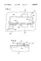
- FIGS. 1-3An improved transistor 100 or multiple gate transistor including the structure of a first embodiment and made in accordance with the invention of the present application is shown in FIGS. 1-3.
- the transistor 100is formed on a base layer or semiconductor structure 102 which can be one or more semiconductor layers or structures and includes active or operable portions of semiconductor devices.
- the semiconductor structure 102is formed of silicon in the illustrated embodiment although the invention is applicable to other semiconductor materials.
- a gate structure 104is formed on a first oxide layer 106 formed on the semiconductor structure 102.
- the gate structure 104is illustrated as a multilayer gate stack which may be formed for an array device for which the present invention is initially being used. However, other gate structures can be used and are considered to be within the scope of the present invention.
- the first oxide layer 106includes thin gate oxide regions represented by the region 106A defining active regions of the structure and substantially thicker field oxide regions 106B defining isolation regions. As illustrated, local oxidization of silicon (LOCOS) isolation is utilized; however, it is noted that the invention can be utilized with other well known isolation technologies as will be apparent.
- LOClocal oxidization of silicon
- the multilayer gate stackcomprises a polysilicon gate layer 108, a silicided polysilicon layer 110, an oxide layer 112 and a nitride layer 114.
- a secondary oxide layer 116is formed on the gate structure 104.
- the secondary oxide layer 116may be formed, for example, by a chemical vapor deposition (CVD) of tetraethyl orthosilicate (TEOS) or rapid thermal processor (RTP) oxide (RTO).
- a conductive gate spacer 118is formed around the gate structure 104 on the secondary oxide layer 116 with the conductive gate spacer 118 being removed from a portion 104C of the gate structure 104 to form an aperture in the spacer 118.
- the conductive gate spacer 118can be formed, for example, from titanium suicide (TiSi 2 ).
- a first portion 104A of the gate structure 104serves as a first or actual gate for the transistor 100 while a second portion 104B of the gate structure 104 forms a pseudo gate or conductive spacer connection support to permit separate connection to the conductive gate spacer 118 which serves as a control or second gate 119 for the transistor 100.
- the portion of the conductive gate spacer 118 which is removedis generally on the top of the first portion 104A of the gate structure 104 and can be removed by the reactive ion etching of the TiSi 2 layer which forms the gate spacer 118.
- a first contactis made through or by way of the first portion 104A of the gate structure 104 where the conductive gate spacer 118 has been removed, i.e., by passing through an aperture formed in the spacer 118, and a second contact is made to the conductive gate spacer 118.
- the first portion 104A and the second portion 104B of the gate structure 104may be formed separately from one another.
- Contacting areas 120, 122 for the first gate and second gateare shown in FIG. 1 and in FIG. 2 by contact openings 120A, 122A made through a mask 124, not shown in FIGS. 1 and 3 for clarity of illustration. It is also possible to contact the gate spacer 118 over the first portion 104A of the gate structure 104 where the conductive gate spacer 118 has not been removed. Such connection to the gate spacer 118 is illustrated in FIG. 2 where a portion of the conductive gate spacer 118 is shown and a contact opening 126 is illustrated in dotted lines. While only a single transistor 100 is illustrated in the drawings, the gate structure 104 can be common to a number of transistors and can comprise a wordline for an integrated array or storage device.
- the gate lengthis 0.1 ⁇ m and is electrically isolated from the gate spacer 118 or second gate which is electrically connected to a separate driver.
- the spacer gate or second gate 119preferably is, formed over the thicker field oxide so that the gate-induced drain leakage (GIDL) effect is not aggravated if the potential on the second gate 119 goes negative in the low off state.
- GIDLgate-induced drain leakage
- turn off of the transistor 100can be ensured by use of a negative voltage on the second gate 119.
- the drive current of the transistor 100is like a 0.1 ⁇ m device but the subthreshold voltage and punchthrough are substantially that of a 0.3 ⁇ m device.
- the structure of the transistor 100may be used throughout an integrated circuit; however, it may be preferred to use the structure of the transistor 100 only in critical speed paths of an integrated circuit to gain speed since the drain voltage can be higher than VCC and the BVDSS and subthreshold voltage are substantially higher.
- the remaining devicescan be structured as standard LDD transistors using the spacers in a conventional manner. Some or all of the remaining devices can also be conventional transistors without spacers, i.e., not LDD transistors or transistors of the present invention.
- An integrated circuit combining conventional transistors and/or LDD transistors 128 and the transistors 100is schematically illustrated in FIG. 4 where the transistors 100 can be used to implement output drivers for the integrated circuit. It is also possible to scale down the gate spacer 118 or remove portions of the gate spacer 118 for compaction of the device.
- the transistor 100is initially being used in array devices; however, it should be apparent that the transistor 100 can be used in a large variety of applications to provide the noted improvements in performance.
- the transistor 100can be used in a dynamic random access memory (DRAM) as schematically shown in FIG. 5 where the transistor 100 is connected between a data line 130 and a storage node 132 with the first and second gates of the transistor 100 being driven by rowline drivers 134, 135, respectively.
- DRAMdynamic random access memory
- the voltage swing between off and on for the first gate controlled by the driver 134can be less than the swing between off and on for the second gate controlled by the driver 135. In this way, it is possible to turn off the second gate by driving it to a negative potential and to turn on the second gate by driving it to a potential higher than the on potential for the first gate.
- the transistor 100is used in a semi-static low power DRAM cell as the nMOS read transistor with the parasitic capacitances of the spacer gates or spacer transistors being used for storage, and a pMOS transistor 136 being used as the write transistor for the cell.
- the spacer gate or second gate 119 of the transistor 100is illustrated as two smaller gates to either side of the first gate of the transistor 100 as should be apparent from the foregoing description.
- a method of making the transistor 100comprises forming a gate structure on a first oxide layer on a semiconductor structure and a secondary oxide layer on the gate structure.
- a conductive spaceris formed around the gate structure on the secondary oxide layer and the conductive spacer is removed from a portion of the gate structure to form an aperture in the spacer.
- a first contactis formed to the gate structure through or by way of the portion of the gate structure from which the conductive spacer has been removed, i.e. by passing through the aperture in the spacer.
- a second contactis formed to the conductive spacer.
- a method for making an integrated circuit having conventional LDD transistors and transistors structured as the transistor 100comprises forming gate structures on a first oxide layer on a semiconductor structure and a secondary oxide layer on the gate structures. Conductive spacers are formed around the gate structures. The conductive spacers are utilized to form LDD transistor structures associated with a first number of the gate structures and to form transistor structures of the present invention associated with a second number of the gate structures. The transistor structures of the present invention are formed by removing the conductive spacer from portions of the second number of gate structures and forming first contacts to the second number of gate structures through the apertures corresponding to the portions of the second number of gate structures from which the conductive spacer has been removed. Second contacts are formed to the conductive spacers.
- conventional transistorswhich are neither LDD nor those of the present invention can also be used in the integrated circuit with the conventional transistors being connected to the LDD transistors and/or the transistors of the present application.
- FIGS. 7 and 8An improved transistor 150 including the structure of a second embodiment and made in accordance with the invention of the present application is shown in FIGS. 7 and 8. Structure which is common between the transistor of FIGS. 1-3 and FIGS. 7 and 8 will be labeled with like numbers.
- the transistor 150is formed on a base layer or semiconductor structure 102 which can be one or more semiconductor layers or structures and includes active or operable portions of semiconductor devices.
- the semiconductor structure 102is formed of silicon in the illustrated embodiment although the invention is applicable to other semiconductor materials.
- a gate structure 104is formed on a first oxide layer 106 formed on the semiconductor structure 102.
- the gate structure 104is illustrated as a multilayer gate stack which may be formed for an array device for which the present invention is initially being used. However, other gate structures can be used and are considered to be within the scope of the present invention.
- the multilayer gate stackcomprises a polysilicon gate layer 108, a silicided polysilicon layer 110, an oxide layer 112 and a nitride layer 114.
- a secondary oxide layer 116is formed on the gate structure 104.
- the secondary oxide layer 116may be formed, for example, by a chemical vapor deposition (CVD) of tetraethyl orthosilicate (TEOS) or rapid thermal processor (RTP) oxide (RTO).
- a conductive layer 152is formed around the gate structure 104 on the secondary oxide layer 116 to define a second gate.
- a nonconductive spacer 154is formed over the conductive layer 152 with the nonconductive spacer and the conductive layer thereunder forming a composite spacer. Nonconductive spacer material and a portion of the conductive layer 152 are removed to expose the top of the gate structure 102, i.e., the nitride layer 114, thereby forming an aperture in the composite spacer over the gate structure 104.
- a first contactis then made to the silicided polysilicon layer 110 in a manner similar to that described above relative to the transistor 100 of FIGS. 1-3, for example, at a contacting area 156.
- a second contactis made to a portion 152A of the conductive layer 152 which was not removed, for example, at a contacting area 158.
- the transistor 150provides the same benefits as the transistor 100 but effectively has a nonconductive spacer which can be advantageous since it imposes less limitations on the area which can be used for metalization to form conductors within an integrated circuit including the transistor 150 and therefor is easier to make.
- FIGS. 9 and 10A third embodiment of a multiple gate transistor of the present invention is illustrated in FIGS. 9 and 10.
- a three gate transistor 160is formed on a base layer or semiconductor structure 162 which can be one or more semiconductor layers or structures and includes active or operable portions of semiconductor devices.
- the semiconductor structure 162is formed of silicon in the illustrated embodiment although the invention is applicable to other semiconductor materials.
- a gate structure 164is formed on a first oxide layer 166 formed on the semiconductor structure 162.
- the gate structure 164is illustrated as a polysilicon gate; however, other gate structures can be used and are considered to be within the scope of the present invention.
- a secondary oxide layer 168is formed on the gate structure 164.
- the secondary oxide layer 168may be formed, for example, by a chemical vapor deposition (CVD) of tetraethyl orthosilicate (TEOS) or rapid thermal processor (RTP) oxide (RTO).
- a conductive gate spacer 170is formed, for example from TiSi 2 , around the gate structure 164 on the secondary oxide layer 168. The conductive gate spacer 170 and the secondary oxide 168 are then removed to the top of the gate structure 164 and to the first oxide layer 166 elsewhere.
- Removal of the conductive gate spacer 170 and the secondary oxide 168 over the gate structure 164forms an opening or aperture 172 in the spacer 170 and the secondary oxide 168 through which the gate structure 164 can be contacted.
- the gate spacer 170 and secondary oxide 168are also removed to the first oxide layer 166 or not formed originally at a first end 160A and at a second end 160B of the transistor 160 leaving a first portion 170A of the spacer 170 on a first side of the gate structure 164 on the secondary oxide layer 168 and a second portion 170B of the spacer 170 on a second side of the gate structure 164 on the secondary oxide layer 168.
- the gate structure 164defines a first gate for the transistor 160, the first portion 170A of the conductive spacer 170 defines a second gate for the transistor 160 and the second portion 170B of the conductive spacer 170 forms a third gate for the transistor 160. While a conductive spacer is illustrated in FIGS. 9 and 10, it is noted that if the portion of the spacer adjacent to the secondary oxide layer is conductive, that conductive portion of the spacer will form the second and third gates for the transistor 160 in accordance with the above disclosure relating to the composite spacer of FIGS. 7 and 8.
- a first contactis made to the gate structure 164, for example at a contacting area 174.
- a second contactis made to the first portion 170A the conductive spacer 170 at a contacting area 176, or to the conductive portion of the spacer if a composite spacer is used.
- a third contactis made to the second portion 170B of the spacer 170 at a contacting area 178, or to the conductive portion of the spacer if a composite spacer is used.
- contactis made to the portion 170A of the spacer 170 using conductive spacer material which extends over the field oxide and the polysilicon gate and contact is made to the portion 170B of the spacer 170 using conductive spacer material which connects to a neighboring spacer 180 formed over a spacer support formed by a pseudo gate or polysilicon pad 182.
- the first, second and third contactscan be made using a variety of known techniques.
- FIGS. 11 and 12A fourth embodiment of a multiple gate transistor of the present invention is illustrated in FIGS. 11 and 12.
- a two gate transistor 190is formed on a base layer or semiconductor structure 192 which can be one or more semiconductor layers or structures and includes active or operable portions of semiconductor devices.
- the semiconductor structure 192is formed of silicon in the illustrated embodiment although the invention is applicable to other semiconductor materials.
- a gate structure 194is formed on a first oxide layer 196 formed on the semiconductor structure 192.
- the gate structure 194is illustrated as a polysilicon gate; however, other gate structures can be used and are considered to be within the scope of the present invention.
- a secondary oxide layer 198is formed on the gate structure 194.
- the secondary oxide layer 198may be formed, for example, by a chemical vapor deposition (CVD) of tetraethyl orthosilicate (TEOS) or rapid thermal processor (RTP) oxide (RTO).
- a conductive gate spacer 200is formed, for example from TiSi 2 , on one side 194A of the gate structure 194 on the secondary oxide layer 198.
- the top of the gate structure 194is open for making contact to the gate structure, for example at a contact area 202.
- the gate structure 194defines a first gate for the transistor 190 and the conductive gate spacer 200 defines a second gate for the transistor 190. While a conductive spacer is illustrated in FIGS. 11 and 12, it is noted that if the portion of the spacer adjacent to the secondary oxide layer is conductive, that conductive portion of the spacer will form the second gate for the transistor 190 in accordance with the above disclosure relating to the composite spacer of FIGS. 7 and 8.
- a first contactis made to the gate structure 194, for example at the contact area 202.
- a second contactis made to the conductive spacer 200, for example at a contact area 204, or to the conductive portion of the spacer if a composite spacer is used.
- contactis made to the conductive spacer 200 using conductive spacer material which connects to a neighboring spacer 206 formed over a spacer support formed by a pseudo gate or polysilicon pad 208 with the contact area 204 straddling the spacer 206.
- the contactscan be made at a number of different locations and using a variety of known techniques. Methods of making the transistor embodiments of FIGS. 7-12 are apparent from the foregoing description and the above description made relative to the embodiments of FIGS. 1-3.
Landscapes
- Engineering & Computer Science (AREA)
- Physics & Mathematics (AREA)
- Condensed Matter Physics & Semiconductors (AREA)
- General Physics & Mathematics (AREA)
- Manufacturing & Machinery (AREA)
- Computer Hardware Design (AREA)
- Microelectronics & Electronic Packaging (AREA)
- Power Engineering (AREA)
- Metal-Oxide And Bipolar Metal-Oxide Semiconductor Integrated Circuits (AREA)
- Insulated Gate Type Field-Effect Transistor (AREA)
Abstract
Description
Claims (14)
Priority Applications (1)
| Application Number | Priority Date | Filing Date | Title |
|---|---|---|---|
| US09/375,102US6090693A (en) | 1996-10-31 | 1999-08-16 | Transistors having controlled conductive spacers, uses of such transistors and methods of making such transistors |
Applications Claiming Priority (3)
| Application Number | Priority Date | Filing Date | Title |
|---|---|---|---|
| US08/741,828US5714786A (en) | 1996-10-31 | 1996-10-31 | Transistors having controlled conductive spacers, uses of such transistors and methods of making such transistors |
| US08/987,819US6005273A (en) | 1996-10-31 | 1997-12-10 | Transistors having controlled conductive spacers, uses of such transistors and methods of making such transistors |
| US09/375,102US6090693A (en) | 1996-10-31 | 1999-08-16 | Transistors having controlled conductive spacers, uses of such transistors and methods of making such transistors |
Related Parent Applications (1)
| Application Number | Title | Priority Date | Filing Date |
|---|---|---|---|
| US08/987,819DivisionUS6005273A (en) | 1996-10-31 | 1997-12-10 | Transistors having controlled conductive spacers, uses of such transistors and methods of making such transistors |
Publications (1)
| Publication Number | Publication Date |
|---|---|
| US6090693Atrue US6090693A (en) | 2000-07-18 |
Family
ID=24982382
Family Applications (4)
| Application Number | Title | Priority Date | Filing Date |
|---|---|---|---|
| US08/741,828Expired - LifetimeUS5714786A (en) | 1996-10-31 | 1996-10-31 | Transistors having controlled conductive spacers, uses of such transistors and methods of making such transistors |
| US08/987,819Expired - LifetimeUS6005273A (en) | 1996-10-31 | 1997-12-10 | Transistors having controlled conductive spacers, uses of such transistors and methods of making such transistors |
| US09/375,081Expired - Fee RelatedUS7005710B1 (en) | 1996-10-31 | 1999-08-16 | Transistors having controlled conductive spacers, uses of such transistors and methods of making such transistors |
| US09/375,102Expired - LifetimeUS6090693A (en) | 1996-10-31 | 1999-08-16 | Transistors having controlled conductive spacers, uses of such transistors and methods of making such transistors |
Family Applications Before (3)
| Application Number | Title | Priority Date | Filing Date |
|---|---|---|---|
| US08/741,828Expired - LifetimeUS5714786A (en) | 1996-10-31 | 1996-10-31 | Transistors having controlled conductive spacers, uses of such transistors and methods of making such transistors |
| US08/987,819Expired - LifetimeUS6005273A (en) | 1996-10-31 | 1997-12-10 | Transistors having controlled conductive spacers, uses of such transistors and methods of making such transistors |
| US09/375,081Expired - Fee RelatedUS7005710B1 (en) | 1996-10-31 | 1999-08-16 | Transistors having controlled conductive spacers, uses of such transistors and methods of making such transistors |
Country Status (1)
| Country | Link |
|---|---|
| US (4) | US5714786A (en) |
Cited By (21)
| Publication number | Priority date | Publication date | Assignee | Title |
|---|---|---|---|---|
| US6368986B1 (en) | 2000-08-31 | 2002-04-09 | Micron Technology, Inc. | Use of selective ozone TEOS oxide to create variable thickness layers and spacers |
| US6503851B2 (en) | 2000-08-31 | 2003-01-07 | Micron Technology, Inc. | Use of linear injectors to deposit uniform selective ozone TEOS oxide film by pulsing reactants on and off |
| US20030148843A1 (en)* | 2001-10-19 | 2003-08-07 | Bowen Thomas C. | Drivetrain with hybrid transfer case |
| US6630724B1 (en) | 2000-08-31 | 2003-10-07 | Micron Technology, Inc. | Gate dielectric antifuse circuits and methods for operating same |
| US6656825B2 (en)* | 2002-04-30 | 2003-12-02 | Advanced Micro Devices, Inc. | Semiconductor device having an improved local interconnect structure and a method for forming such a device |
| US6661055B2 (en)* | 2001-11-17 | 2003-12-09 | Hynix Semiconductor Inc. | Transistor in semiconductor devices |
| US20040041167A1 (en)* | 2002-08-29 | 2004-03-04 | Micron Technology, Inc. | Gate dielectric antifuse circuit to protect a high-voltage transistor |
| US20040042317A1 (en)* | 2002-08-29 | 2004-03-04 | Micron Technology, Inc. | Circuits and methods to protect a gate dielectric antifuse |
| US20040137689A1 (en)* | 2003-01-15 | 2004-07-15 | International Business Machines Corporation | Low-GIDL MOSFET structure and method for fabrication |
| US6798013B2 (en) | 2002-08-28 | 2004-09-28 | Fernando Gonzalez | Vertically integrated flash memory cell and method of fabricating a vertically integrated flash memory cell |
| EP1478013A3 (en)* | 2003-05-16 | 2006-08-02 | Agere Systems Inc. | Split-gate metal-oxide-semiconductor device |
| US20070284673A1 (en)* | 2006-06-13 | 2007-12-13 | Stmicroelectronics S.R.L. | High frequency MOS device and manufacturing process thereof |
| US20080012056A1 (en)* | 2006-07-17 | 2008-01-17 | Micron Technology, Inc. | Capacitorless one transistor dram cell, integrated circuitry comprising an array of capacitorless one transistor dram cells, and method of forming lines of capacitorless one transistor dram cells |
| US20080061346A1 (en)* | 2006-09-07 | 2008-03-13 | Micron Technology, Inc. | One-transistor memory cell with bias gate |
| US20080142882A1 (en)* | 2004-09-01 | 2008-06-19 | Tang Sanh D | Transistors |
| US7700441B2 (en) | 2006-02-02 | 2010-04-20 | Micron Technology, Inc. | Methods of forming field effect transistors, methods of forming field effect transistor gates, methods of forming integrated circuitry comprising a transistor gate array and circuitry peripheral to the gate array, and methods of forming integrated circuitry comprising a transistor gate array including first gates and second grounded isolation gates |
| US7772632B2 (en) | 2006-08-21 | 2010-08-10 | Micron Technology, Inc. | Memory arrays and methods of fabricating memory arrays |
| US7867851B2 (en) | 2005-08-30 | 2011-01-11 | Micron Technology, Inc. | Methods of forming field effect transistors on substrates |
| US7897460B2 (en) | 2005-03-25 | 2011-03-01 | Micron Technology, Inc. | Methods of forming recessed access devices associated with semiconductor constructions |
| US8399920B2 (en) | 2005-07-08 | 2013-03-19 | Werner Juengling | Semiconductor device comprising a transistor gate having multiple vertically oriented sidewalls |
| US10515801B2 (en) | 2007-06-04 | 2019-12-24 | Micron Technology, Inc. | Pitch multiplication using self-assembling materials |
Families Citing this family (15)
| Publication number | Priority date | Publication date | Assignee | Title |
|---|---|---|---|---|
| US5714786A (en) | 1996-10-31 | 1998-02-03 | Micron Technology, Inc. | Transistors having controlled conductive spacers, uses of such transistors and methods of making such transistors |
| JPH10270380A (en)* | 1997-03-21 | 1998-10-09 | Nec Corp | Semiconductor device |
| US5846871A (en)* | 1997-08-26 | 1998-12-08 | Lucent Technologies Inc. | Integrated circuit fabrication |
| JPH11220112A (en)* | 1998-01-30 | 1999-08-10 | Mitsubishi Electric Corp | Semiconductor device and manufacturing method thereof |
| JP4030193B2 (en) | 1998-07-16 | 2008-01-09 | 株式会社半導体エネルギー研究所 | Method for manufacturing semiconductor device |
| JP3592535B2 (en)* | 1998-07-16 | 2004-11-24 | 株式会社半導体エネルギー研究所 | Method for manufacturing semiconductor device |
| US6097070A (en)* | 1999-02-16 | 2000-08-01 | International Business Machines Corporation | MOSFET structure and process for low gate induced drain leakage (GILD) |
| KR100332125B1 (en) | 1999-06-30 | 2002-04-10 | 박종섭 | Mothod of manufacturing a CMOS transistor |
| US6252284B1 (en)* | 1999-12-09 | 2001-06-26 | International Business Machines Corporation | Planarized silicon fin device |
| US6891234B1 (en)* | 2004-01-07 | 2005-05-10 | Acorn Technologies, Inc. | Transistor with workfunction-induced charge layer |
| US6909145B2 (en)* | 2002-09-23 | 2005-06-21 | International Business Machines Corporation | Metal spacer gate for CMOS FET |
| US6967143B2 (en)* | 2003-04-30 | 2005-11-22 | Freescale Semiconductor, Inc. | Semiconductor fabrication process with asymmetrical conductive spacers |
| US7192876B2 (en) | 2003-05-22 | 2007-03-20 | Freescale Semiconductor, Inc. | Transistor with independent gate structures |
| DE102006060342A1 (en)* | 2006-12-20 | 2008-06-26 | Texas Instruments Deutschland Gmbh | CMOS transistor |
| US8969928B2 (en)* | 2010-08-31 | 2015-03-03 | Micron Technology, Inc. | Transistors having a control gate and one or more conductive structures |
Citations (23)
| Publication number | Priority date | Publication date | Assignee | Title |
|---|---|---|---|---|
| US4213139A (en)* | 1978-05-18 | 1980-07-15 | Texas Instruments Incorporated | Double level polysilicon series transistor cell |
| US4319263A (en)* | 1978-05-18 | 1982-03-09 | Texas Instruments Incorporated | Double level polysilicon series transistor devices |
| US4472821A (en)* | 1982-05-03 | 1984-09-18 | General Electric Company | Dynamic shift register utilizing CMOS dual gate transistors |
| US4975385A (en)* | 1990-04-06 | 1990-12-04 | Applied Materials, Inc. | Method of constructing lightly doped drain (LDD) integrated circuit structure |
| US5115288A (en)* | 1990-06-28 | 1992-05-19 | National Semiconductor Corporation | Split-gate EPROM cell using polysilicon spacers |
| US5250450A (en)* | 1991-04-08 | 1993-10-05 | Micron Technology, Inc. | Insulated-gate vertical field-effect transistor with high current drive and minimum overlap capacitance |
| US5252504A (en)* | 1988-05-02 | 1993-10-12 | Micron Technology, Inc. | Reverse polysilicon CMOS fabrication |
| US5257238A (en)* | 1991-07-11 | 1993-10-26 | Micron Technology, Inc. | Dynamic memory having access transistor turn-off state |
| US5292681A (en)* | 1993-09-16 | 1994-03-08 | Micron Semiconductor, Inc. | Method of processing a semiconductor wafer to form an array of nonvolatile memory devices employing floating gate transistors and peripheral area having CMOS transistors |
| US5324960A (en)* | 1993-01-19 | 1994-06-28 | Motorola, Inc. | Dual-transistor structure and method of formation |
| US5397727A (en)* | 1994-07-20 | 1995-03-14 | Micron Technology, Inc. | Method of forming a floating gate programmable read only memory cell transistor |
| US5425392A (en)* | 1993-05-26 | 1995-06-20 | Micron Semiconductor, Inc. | Method DRAM polycide rowline formation |
| US5439835A (en)* | 1993-11-12 | 1995-08-08 | Micron Semiconductor, Inc. | Process for DRAM incorporating a high-energy, oblique P-type implant for both field isolation and punchthrough |
| US5460996A (en)* | 1993-09-09 | 1995-10-24 | Hyundai Electronics Industries Co. Ltd. | Method for the fabrication of a stacked capacitor all in the dynamic semiconductor memory device |
| US5495441A (en)* | 1994-05-18 | 1996-02-27 | United Microelectronics Corporation | Split-gate flash memory cell |
| US5495411A (en)* | 1993-12-22 | 1996-02-27 | Ananda; Mohan | Secure software rental system using continuous asynchronous password verification |
| US5513137A (en)* | 1995-02-23 | 1996-04-30 | Micron Technology, Inc. | Flash memory having transistor redundancy |
| US5600168A (en)* | 1994-04-20 | 1997-02-04 | Lg Semicon Co., Ltd. | Semiconductor element and method for fabricating the same |
| US5599726A (en)* | 1995-12-04 | 1997-02-04 | Chartered Semiconductor Manufacturing Pte Ltd | Method of making a conductive spacer lightly doped drain (LDD) for hot carrier effect (HCE) control |
| US5714786A (en)* | 1996-10-31 | 1998-02-03 | Micron Technology, Inc. | Transistors having controlled conductive spacers, uses of such transistors and methods of making such transistors |
| US5789297A (en)* | 1996-09-23 | 1998-08-04 | Mosel Vitelic Inc. | Method of making EEPROM cell device with polyspacer floating gate |
| US5817561A (en)* | 1996-09-30 | 1998-10-06 | Motorola, Inc. | Insulated gate semiconductor device and method of manufacture |
| US5869376A (en)* | 1995-09-08 | 1999-02-09 | Nippon Steel Semiconductor Corporation | Production method for semiconductor device having field-shield isolation structure |
- 1996
- 1996-10-31USUS08/741,828patent/US5714786A/ennot_activeExpired - Lifetime
- 1997
- 1997-12-10USUS08/987,819patent/US6005273A/ennot_activeExpired - Lifetime
- 1999
- 1999-08-16USUS09/375,081patent/US7005710B1/ennot_activeExpired - Fee Related
- 1999-08-16USUS09/375,102patent/US6090693A/ennot_activeExpired - Lifetime
Patent Citations (23)
| Publication number | Priority date | Publication date | Assignee | Title |
|---|---|---|---|---|
| US4319263A (en)* | 1978-05-18 | 1982-03-09 | Texas Instruments Incorporated | Double level polysilicon series transistor devices |
| US4213139A (en)* | 1978-05-18 | 1980-07-15 | Texas Instruments Incorporated | Double level polysilicon series transistor cell |
| US4472821A (en)* | 1982-05-03 | 1984-09-18 | General Electric Company | Dynamic shift register utilizing CMOS dual gate transistors |
| US5252504A (en)* | 1988-05-02 | 1993-10-12 | Micron Technology, Inc. | Reverse polysilicon CMOS fabrication |
| US4975385A (en)* | 1990-04-06 | 1990-12-04 | Applied Materials, Inc. | Method of constructing lightly doped drain (LDD) integrated circuit structure |
| US5115288A (en)* | 1990-06-28 | 1992-05-19 | National Semiconductor Corporation | Split-gate EPROM cell using polysilicon spacers |
| US5250450A (en)* | 1991-04-08 | 1993-10-05 | Micron Technology, Inc. | Insulated-gate vertical field-effect transistor with high current drive and minimum overlap capacitance |
| US5257238A (en)* | 1991-07-11 | 1993-10-26 | Micron Technology, Inc. | Dynamic memory having access transistor turn-off state |
| US5324960A (en)* | 1993-01-19 | 1994-06-28 | Motorola, Inc. | Dual-transistor structure and method of formation |
| US5425392A (en)* | 1993-05-26 | 1995-06-20 | Micron Semiconductor, Inc. | Method DRAM polycide rowline formation |
| US5460996A (en)* | 1993-09-09 | 1995-10-24 | Hyundai Electronics Industries Co. Ltd. | Method for the fabrication of a stacked capacitor all in the dynamic semiconductor memory device |
| US5292681A (en)* | 1993-09-16 | 1994-03-08 | Micron Semiconductor, Inc. | Method of processing a semiconductor wafer to form an array of nonvolatile memory devices employing floating gate transistors and peripheral area having CMOS transistors |
| US5439835A (en)* | 1993-11-12 | 1995-08-08 | Micron Semiconductor, Inc. | Process for DRAM incorporating a high-energy, oblique P-type implant for both field isolation and punchthrough |
| US5495411A (en)* | 1993-12-22 | 1996-02-27 | Ananda; Mohan | Secure software rental system using continuous asynchronous password verification |
| US5600168A (en)* | 1994-04-20 | 1997-02-04 | Lg Semicon Co., Ltd. | Semiconductor element and method for fabricating the same |
| US5495441A (en)* | 1994-05-18 | 1996-02-27 | United Microelectronics Corporation | Split-gate flash memory cell |
| US5397727A (en)* | 1994-07-20 | 1995-03-14 | Micron Technology, Inc. | Method of forming a floating gate programmable read only memory cell transistor |
| US5513137A (en)* | 1995-02-23 | 1996-04-30 | Micron Technology, Inc. | Flash memory having transistor redundancy |
| US5869376A (en)* | 1995-09-08 | 1999-02-09 | Nippon Steel Semiconductor Corporation | Production method for semiconductor device having field-shield isolation structure |
| US5599726A (en)* | 1995-12-04 | 1997-02-04 | Chartered Semiconductor Manufacturing Pte Ltd | Method of making a conductive spacer lightly doped drain (LDD) for hot carrier effect (HCE) control |
| US5789297A (en)* | 1996-09-23 | 1998-08-04 | Mosel Vitelic Inc. | Method of making EEPROM cell device with polyspacer floating gate |
| US5817561A (en)* | 1996-09-30 | 1998-10-06 | Motorola, Inc. | Insulated gate semiconductor device and method of manufacture |
| US5714786A (en)* | 1996-10-31 | 1998-02-03 | Micron Technology, Inc. | Transistors having controlled conductive spacers, uses of such transistors and methods of making such transistors |
Non-Patent Citations (8)
| Title |
|---|
| F. C. Hsu and K. Y. Chiu, Article from IEEE Electron Device Letters, vol. EDL 5, No. 5, entitled: Evaluation of LDD MOSFET s Based on Hot Electron Induced Degradation , May 1984, pp. 162 165.* |
| F. -C. Hsu and K.-Y. Chiu, Article from IEEE Electron Device Letters, vol. EDL-5, No. 5, entitled: "Evaluation of LDD MOSFET's Based on Hot-Electron-Induced Degradation", May 1984, pp. 162-165. |
| I.C. Chen, J. P. Lin, and C. W. Teng, Article from 1990 Symposium on VlSI Technology entitled: "A Highly Reliable 0.3 u N-channel MOSFET Using Poly Spacers", pp. 39-40. |
| I.C. Chen, J. P. Lin, and C. W. Teng, Article from 1990 Symposium on VlSI Technology entitled: A Highly Reliable 0.3 u N channel MOSFET Using Poly Spacers , pp. 39 40.* |
| Masataka Minami, Yasuo Sawahata, Hiroshi Matsuki and Takahiro Nagano, Article from 1990 Symposium on VLSI Technology entitiled: A High Speed & High Reality MOFSET Utilizing an Auxiliary Gate, pp. 41 42.* |
| Masataka Minami, Yasuo Sawahata, Hiroshi Matsuki and Takahiro Nagano, Article from 1990 Symposium on VLSI Technology entitiled: A High Speed & High Reality MOFSET Utilizing an Auxiliary Gate, pp. 41-42. |
| Tiao yuan Huang, William W. Yao, Russell A. Martin, Alan G. Lewis, Mitsumasa Koyanagi, & John Y Chen, A Novel Submicron LDD Transistor with Inverse T Gate Structure, IDEM 1986, pp. 742 745.* |
| Tiao-yuan Huang, William W. Yao, Russell A. Martin, Alan G. Lewis, Mitsumasa Koyanagi, & John Y Chen, A Novel Submicron LDD Transistor with Inverse-T Gate Structure, IDEM 1986, pp. 742-745. |
Cited By (64)
| Publication number | Priority date | Publication date | Assignee | Title |
|---|---|---|---|---|
| US6368986B1 (en) | 2000-08-31 | 2002-04-09 | Micron Technology, Inc. | Use of selective ozone TEOS oxide to create variable thickness layers and spacers |
| US20020098633A1 (en)* | 2000-08-31 | 2002-07-25 | William Budge | Use of selective ozone TEOS oxide to create variable thickness layers and spacers |
| US6503851B2 (en) | 2000-08-31 | 2003-01-07 | Micron Technology, Inc. | Use of linear injectors to deposit uniform selective ozone TEOS oxide film by pulsing reactants on and off |
| US6602807B2 (en) | 2000-08-31 | 2003-08-05 | Micron Technology, Inc. | Use of linear injectors to deposit uniform selective ozone TEOS oxide film by pulsing reactants on and off |
| US7030458B2 (en) | 2000-08-31 | 2006-04-18 | Micron Technology, Inc. | Gate dielectric antifuse circuits and methods for operating same |
| US6617230B2 (en)* | 2000-08-31 | 2003-09-09 | Micron Technology, Inc. | Use of selective ozone teos oxide to create variable thickness layers and spacers |
| US6630724B1 (en) | 2000-08-31 | 2003-10-07 | Micron Technology, Inc. | Gate dielectric antifuse circuits and methods for operating same |
| US20060097345A1 (en)* | 2000-08-31 | 2006-05-11 | Micron Technology, Inc. | Gate dielectric antifuse circuits and methods for operating same |
| US20040029402A1 (en)* | 2000-08-31 | 2004-02-12 | William Budge | Use of linear injectors to deposit uniform selective ozone TEOS oxide film by pulsing reactants on and off |
| US20050035418A1 (en)* | 2000-08-31 | 2005-02-17 | Micron Technology, Inc. | Selectively deposited silicon oxide layers on a silicon substrate |
| US20040065941A1 (en)* | 2000-08-31 | 2004-04-08 | Micron Technology, Inc. | Gate dielectric antifuse circuits and methods for operating same |
| US7214979B2 (en) | 2000-08-31 | 2007-05-08 | Micron Technology, Inc. | Selectively deposited silicon oxide layers on a silicon substrate |
| US7192893B2 (en) | 2000-08-31 | 2007-03-20 | Micron Technology Inc. | Use of linear injectors to deposit uniform selective ozone TEOS oxide film by pulsing reactants on and off |
| US20030148843A1 (en)* | 2001-10-19 | 2003-08-07 | Bowen Thomas C. | Drivetrain with hybrid transfer case |
| US6661055B2 (en)* | 2001-11-17 | 2003-12-09 | Hynix Semiconductor Inc. | Transistor in semiconductor devices |
| DE10219361B4 (en)* | 2002-04-30 | 2008-04-30 | Advanced Micro Devices, Inc., Sunnyvale | A semiconductor device having an improved local interconnect structure and a method of making such an element |
| US6656825B2 (en)* | 2002-04-30 | 2003-12-02 | Advanced Micro Devices, Inc. | Semiconductor device having an improved local interconnect structure and a method for forming such a device |
| US7098122B2 (en) | 2002-08-28 | 2006-08-29 | Micron Technology, Inc. | Method of fabricating a vertically integrated memory cell |
| US6798013B2 (en) | 2002-08-28 | 2004-09-28 | Fernando Gonzalez | Vertically integrated flash memory cell and method of fabricating a vertically integrated flash memory cell |
| US20050139950A1 (en)* | 2002-08-28 | 2005-06-30 | Fernando Gonzalez | Vertically integrated flash memory cell and method of fabricating a vertically integrated flash memory cell |
| US20040155315A1 (en)* | 2002-08-29 | 2004-08-12 | Micron Technology, Inc. | Circuits and methods to protect a gate dielectric antifuse |
| US7126871B2 (en) | 2002-08-29 | 2006-10-24 | Micron Technology, Inc. | Circuits and methods to protect a gate dielectric antifuse |
| US20050029598A1 (en)* | 2002-08-29 | 2005-02-10 | Micron Technology, Inc. | Gate dielectric antifuse circuit to protect a high-voltage transistor |
| US6936909B2 (en) | 2002-08-29 | 2005-08-30 | Micron Technology, Inc. | Gate dielectric antifuse circuit to protect a high-voltage transistor |
| US20040041167A1 (en)* | 2002-08-29 | 2004-03-04 | Micron Technology, Inc. | Gate dielectric antifuse circuit to protect a high-voltage transistor |
| US7405463B2 (en) | 2002-08-29 | 2008-07-29 | Micron Technology, Inc. | Gate dielectric antifuse circuit to protect a high-voltage transistor |
| US20040042317A1 (en)* | 2002-08-29 | 2004-03-04 | Micron Technology, Inc. | Circuits and methods to protect a gate dielectric antifuse |
| US6751150B2 (en) | 2002-08-29 | 2004-06-15 | Micron Technology, Inc. | Circuits and method to protect a gate dielectric antifuse |
| US7101738B2 (en) | 2002-08-29 | 2006-09-05 | Micron Technology, Inc. | Gate dielectric antifuse circuit to protect a high-voltage transistor |
| US20060231922A1 (en)* | 2002-08-29 | 2006-10-19 | Micron Technology, Inc. | Gate dielectric antifuse circuit to protect a high-voltage transistor |
| US6841826B2 (en) | 2003-01-15 | 2005-01-11 | International Business Machines Corporation | Low-GIDL MOSFET structure and method for fabrication |
| US20040137689A1 (en)* | 2003-01-15 | 2004-07-15 | International Business Machines Corporation | Low-GIDL MOSFET structure and method for fabrication |
| US6878582B2 (en) | 2003-01-15 | 2005-04-12 | International Business Machines Corporation | Low-GIDL MOSFET structure and method for fabrication |
| US20040248356A1 (en)* | 2003-01-15 | 2004-12-09 | International Business Machines Corporation | Low-GIDL MOSFET structure and method for fabrication |
| EP1478013A3 (en)* | 2003-05-16 | 2006-08-02 | Agere Systems Inc. | Split-gate metal-oxide-semiconductor device |
| US8120101B2 (en) | 2004-09-01 | 2012-02-21 | Micron Technology, Inc. | Semiconductor constructions and transistors, and methods of forming semiconductor constructions and transistors |
| US20080142882A1 (en)* | 2004-09-01 | 2008-06-19 | Tang Sanh D | Transistors |
| US7825462B2 (en) | 2004-09-01 | 2010-11-02 | Micron Technology, Inc. | Transistors |
| US8067286B2 (en) | 2005-03-25 | 2011-11-29 | Micron Technology, Inc. | Methods of forming recessed access devices associated with semiconductor constructions |
| US7897460B2 (en) | 2005-03-25 | 2011-03-01 | Micron Technology, Inc. | Methods of forming recessed access devices associated with semiconductor constructions |
| US8916912B2 (en) | 2005-07-08 | 2014-12-23 | Micron Technology, Inc. | Semiconductor device comprising a transistor gate having multiple vertically oriented sidewalls |
| US9536971B2 (en) | 2005-07-08 | 2017-01-03 | Micron Technology, Inc. | Semiconductor device comprising a transistor gate having multiple vertically oriented sidewalls |
| US8399920B2 (en) | 2005-07-08 | 2013-03-19 | Werner Juengling | Semiconductor device comprising a transistor gate having multiple vertically oriented sidewalls |
| US8877589B2 (en) | 2005-08-30 | 2014-11-04 | Micron Technology, Inc. | Methods of forming field effect transistors on substrates |
| US7867851B2 (en) | 2005-08-30 | 2011-01-11 | Micron Technology, Inc. | Methods of forming field effect transistors on substrates |
| US8426273B2 (en) | 2005-08-30 | 2013-04-23 | Micron Technology, Inc. | Methods of forming field effect transistors on substrates |
| US7700441B2 (en) | 2006-02-02 | 2010-04-20 | Micron Technology, Inc. | Methods of forming field effect transistors, methods of forming field effect transistor gates, methods of forming integrated circuitry comprising a transistor gate array and circuitry peripheral to the gate array, and methods of forming integrated circuitry comprising a transistor gate array including first gates and second grounded isolation gates |
| US8389363B2 (en) | 2006-02-02 | 2013-03-05 | Micron Technology, Inc. | Methods of forming field effect transistors, methods of forming field effect transistor gates, methods of forming integrated circuitry comprising a transistor gate array and circuitry peripheral to the gate array, and methods of forming integrated circuitry comprising a transistor gate array including first gates and second grounded isolation gates |
| US7902028B2 (en) | 2006-02-02 | 2011-03-08 | Micron Technology, Inc. | Methods of forming field effect transistors, methods of forming field effect transistor gates, methods of forming integrated circuitry comprising a transistor gate array and circuitry peripheral to the gate array, and methods of forming integrated circuitry comprising a transistor gate array including first gates and second grounded isolation gates |
| US8334576B2 (en)* | 2006-06-13 | 2012-12-18 | Stmicroelectronics S.R.L. | High frequency MOS device and manufacturing process thereof |
| US20070284673A1 (en)* | 2006-06-13 | 2007-12-13 | Stmicroelectronics S.R.L. | High frequency MOS device and manufacturing process thereof |
| EP1868247A1 (en)* | 2006-06-13 | 2007-12-19 | STMicroelectronics S.r.l. | High frequency MOS device and manufacturing process thereof |
| US8551823B2 (en) | 2006-07-17 | 2013-10-08 | Micron Technology, Inc. | Methods of forming lines of capacitorless one transistor DRAM cells, methods of patterning substrates, and methods of forming two conductive lines |
| US7602001B2 (en) | 2006-07-17 | 2009-10-13 | Micron Technology, Inc. | Capacitorless one transistor DRAM cell, integrated circuitry comprising an array of capacitorless one transistor DRAM cells, and method of forming lines of capacitorless one transistor DRAM cells |
| US9129847B2 (en) | 2006-07-17 | 2015-09-08 | Micron Technology, Inc. | Transistor structures and integrated circuitry comprising an array of transistor structures |
| US20080012056A1 (en)* | 2006-07-17 | 2008-01-17 | Micron Technology, Inc. | Capacitorless one transistor dram cell, integrated circuitry comprising an array of capacitorless one transistor dram cells, and method of forming lines of capacitorless one transistor dram cells |
| EP2772942A2 (en) | 2006-07-17 | 2014-09-03 | Micron Technology, Inc. | Capacitorless one transistor dram cell, integrated circuitry comprising an array of capacitorless one transistor dram cells, and method of forming lines of capacitorless one transistor dram cells |
| US8394699B2 (en) | 2006-08-21 | 2013-03-12 | Micron Technology, Inc. | Memory arrays and methods of fabricating memory arrays |
| US7772632B2 (en) | 2006-08-21 | 2010-08-10 | Micron Technology, Inc. | Memory arrays and methods of fabricating memory arrays |
| US8446762B2 (en) | 2006-09-07 | 2013-05-21 | Micron Technology, Inc. | Methods of making a semiconductor memory device |
| US20080061346A1 (en)* | 2006-09-07 | 2008-03-13 | Micron Technology, Inc. | One-transistor memory cell with bias gate |
| US7589995B2 (en) | 2006-09-07 | 2009-09-15 | Micron Technology, Inc. | One-transistor memory cell with bias gate |
| US7944743B2 (en) | 2006-09-07 | 2011-05-17 | Micron Technology, Inc. | Methods of making a semiconductor memory device |
| US10515801B2 (en) | 2007-06-04 | 2019-12-24 | Micron Technology, Inc. | Pitch multiplication using self-assembling materials |
Also Published As
| Publication number | Publication date |
|---|---|
| US6005273A (en) | 1999-12-21 |
| US5714786A (en) | 1998-02-03 |
| US7005710B1 (en) | 2006-02-28 |
Similar Documents
| Publication | Publication Date | Title |
|---|---|---|
| US6090693A (en) | Transistors having controlled conductive spacers, uses of such transistors and methods of making such transistors | |
| US7015543B2 (en) | Trench-gate semiconductor device and fabrication method thereof | |
| US7385259B2 (en) | Method of manufacturing a multilayered doped conductor for a contact in an integrated circuit device | |
| KR100319356B1 (en) | Semiconductor device and method for manufacturing the same | |
| US20050275014A1 (en) | Integration method of a semiconductor device having a recessed gate electrode | |
| US5504027A (en) | Method for fabricating semiconductor memory devices | |
| JP2004214413A (en) | Semiconductor device | |
| JP2004533728A (en) | Field effect transistor and method of manufacturing the same | |
| JP2008537339A (en) | Parallel field effect transistor structure with body contacts | |
| US5654573A (en) | Semiconductor device having SOI structure and manufacturing method therefor | |
| JP4832629B2 (en) | Semiconductor device | |
| KR100486187B1 (en) | Semiconductor device and its manufacturing method | |
| US5296399A (en) | Method for manufacturing a narrowed sidewall spacer in a peripheral circuit of a ULSI semiconductor memory device | |
| US6867445B2 (en) | Semiconductor memory devices including different thickness dielectric layers for the cell transistors and refresh transistors thereof | |
| KR100432940B1 (en) | N-channel metal oxide semiconductor (nmos) driver circuit and method of making same | |
| US7135742B1 (en) | Insulated gate type semiconductor device and method for fabricating same | |
| US20010020722A1 (en) | Step-like silicon on isolation structure | |
| JPH1117129A (en) | Method for manufacturing semiconductor integrated circuit device | |
| JPH11284146A (en) | Semiconductor memory device and method of manufacturing the same | |
| KR100422412B1 (en) | Cylindrical type transistor having vertical silicon-on-insulator structure and fabrication method thereof | |
| US6188111B1 (en) | Dual gate semiconductor device for shortening channel length | |
| JP4309070B2 (en) | Nonvolatile semiconductor memory device and manufacturing method thereof | |
| JP3669070B2 (en) | Semiconductor device and manufacturing method thereof | |
| JPH11354783A (en) | Semiconductor device | |
| JPH1126764A (en) | Manufacture of semiconductor device |
Legal Events
| Date | Code | Title | Description |
|---|---|---|---|
| STCF | Information on status: patent grant | Free format text:PATENTED CASE | |
| FPAY | Fee payment | Year of fee payment:4 | |
| FEPP | Fee payment procedure | Free format text:PAYOR NUMBER ASSIGNED (ORIGINAL EVENT CODE: ASPN); ENTITY STATUS OF PATENT OWNER: LARGE ENTITY | |
| FPAY | Fee payment | Year of fee payment:8 | |
| FPAY | Fee payment | Year of fee payment:12 | |
| AS | Assignment | Owner name:U.S. BANK NATIONAL ASSOCIATION, AS COLLATERAL AGENT, CALIFORNIA Free format text:SECURITY INTEREST;ASSIGNOR:MICRON TECHNOLOGY, INC.;REEL/FRAME:038669/0001 Effective date:20160426 Owner name:U.S. BANK NATIONAL ASSOCIATION, AS COLLATERAL AGEN Free format text:SECURITY INTEREST;ASSIGNOR:MICRON TECHNOLOGY, INC.;REEL/FRAME:038669/0001 Effective date:20160426 | |
| AS | Assignment | Owner name:MORGAN STANLEY SENIOR FUNDING, INC., AS COLLATERAL AGENT, MARYLAND Free format text:PATENT SECURITY AGREEMENT;ASSIGNOR:MICRON TECHNOLOGY, INC.;REEL/FRAME:038954/0001 Effective date:20160426 Owner name:MORGAN STANLEY SENIOR FUNDING, INC., AS COLLATERAL Free format text:PATENT SECURITY AGREEMENT;ASSIGNOR:MICRON TECHNOLOGY, INC.;REEL/FRAME:038954/0001 Effective date:20160426 | |
| AS | Assignment | Owner name:U.S. BANK NATIONAL ASSOCIATION, AS COLLATERAL AGENT, CALIFORNIA Free format text:CORRECTIVE ASSIGNMENT TO CORRECT THE REPLACE ERRONEOUSLY FILED PATENT #7358718 WITH THE CORRECT PATENT #7358178 PREVIOUSLY RECORDED ON REEL 038669 FRAME 0001. ASSIGNOR(S) HEREBY CONFIRMS THE SECURITY INTEREST;ASSIGNOR:MICRON TECHNOLOGY, INC.;REEL/FRAME:043079/0001 Effective date:20160426 Owner name:U.S. BANK NATIONAL ASSOCIATION, AS COLLATERAL AGEN Free format text:CORRECTIVE ASSIGNMENT TO CORRECT THE REPLACE ERRONEOUSLY FILED PATENT #7358718 WITH THE CORRECT PATENT #7358178 PREVIOUSLY RECORDED ON REEL 038669 FRAME 0001. ASSIGNOR(S) HEREBY CONFIRMS THE SECURITY INTEREST;ASSIGNOR:MICRON TECHNOLOGY, INC.;REEL/FRAME:043079/0001 Effective date:20160426 | |
| AS | Assignment | Owner name:MICRON TECHNOLOGY, INC., IDAHO Free format text:RELEASE BY SECURED PARTY;ASSIGNOR:U.S. BANK NATIONAL ASSOCIATION, AS COLLATERAL AGENT;REEL/FRAME:047243/0001 Effective date:20180629 | |
| AS | Assignment | Owner name:MICRON TECHNOLOGY, INC., IDAHO Free format text:RELEASE BY SECURED PARTY;ASSIGNOR:MORGAN STANLEY SENIOR FUNDING, INC., AS COLLATERAL AGENT;REEL/FRAME:050937/0001 Effective date:20190731 |